Integrated RF design Flow From Concept to Fabrication Using ADS dist_BPF1_1 ModelType=MW Delta=0 mil Zo=50 Ohm N=0 As=20 dB Ap=3 dB Fs2=2.4 GHz Fp2=2.2 GHz Fp1=2 GHz Fs1=1.8 GHz Subst="MSub1" dist_BPF1 Re f PAD_PI_Design_1 ModelType=MW Loss=0. dB PAD_PI_Design BoardLayout1_1 ModelType=MW BoardLayout1 Ref BPF2_lumped_design_lay_1 ModelType=MW BPF2_lumped_design_lay MIX1 Mixer2 PAD_PI_Design_1 ModelType=MW Loss=0. dB PAD_PI_Design AMP1 Amplifier2 EM Modeled RF Board In house designed Bought out

Welcome message from author
This document is posted to help you gain knowledge. Please leave a comment to let me know what you think about it! Share it to your friends and learn new things together.
Transcript
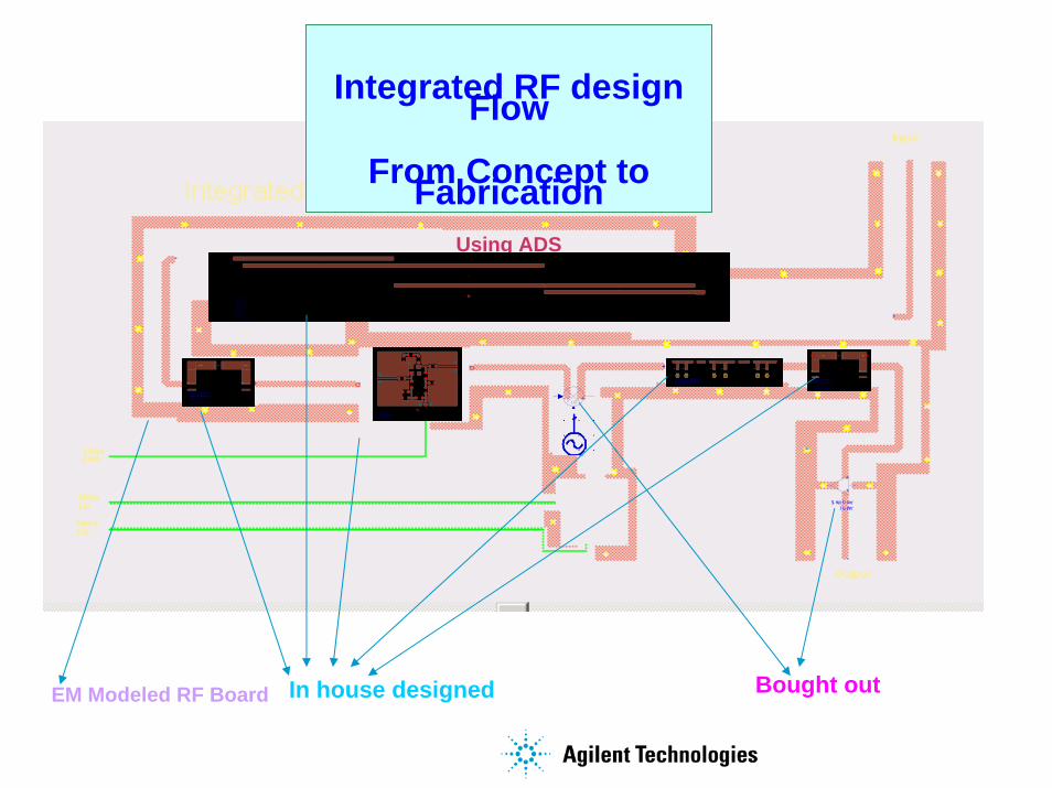
Integrated RF design Flow
From Concept to FabricationUsing ADS
d i s t_ B PF 1 _ 1
M o d e l T y p e = M WDe l ta = 0 m i lZ o = 5 0 Oh mN= 0A s = 2 0 d BA p = 3 d BF s 2 = 2 .4 GHzF p 2 = 2 .2 GHzF p 1 = 2 GHzF s 1 = 1 .8 GHzS u b s t= "M Su b 1 "
d i s t_ B PF 1Re f
T L 1
C L in 1
C L in 3
T L 2
C L in 2
PAD_PI_Design_1
ModelType=MWLoss=0. dB
PAD_PI_Design
Gc Tee1
Gb
Tee3
Ga
BoardLayout1_1ModelType=MW
BoardLayout1Ref
BPF2_lumped_design_lay_1ModelType=MW
BPF2_lumped_design_lay
L1
L2
L3
L4
L5C 1
C2
C 3
C4
C 5
X1 X2 X3 X4 X6X7
MIX1Mixer2
PAD_PI_Design_1
ModelType=MWLoss=0. dB
PAD_PI_Design
Gc Tee1
Gb
Tee3
Ga
AMP1
Amplifier2
EM Modeled RF Board In house designed Bought out
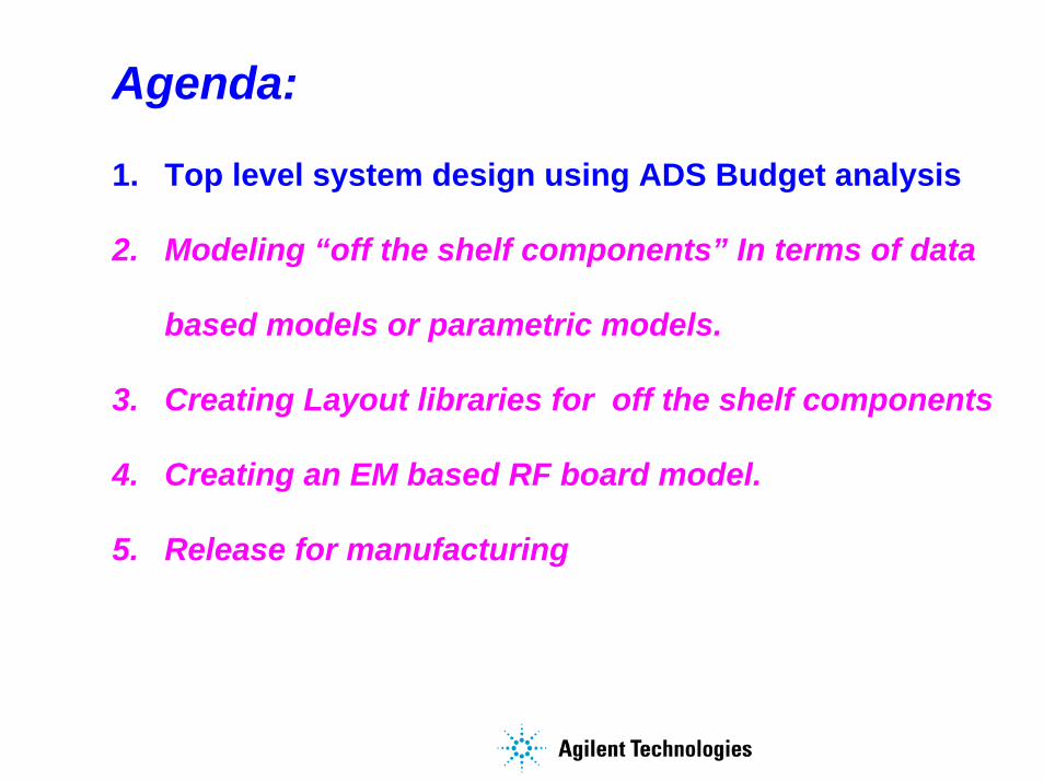
Agenda:
1. Top level system design using ADS Budget analysis
2. Modeling “off the shelf components” In terms of data
based models or parametric models.
3. Creating Layout libraries for off the shelf components
4. Creating an EM based RF board model.
5. Release for manufacturing
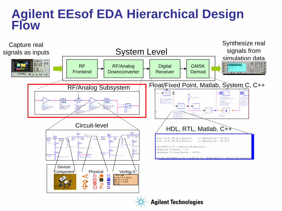
Agilent EEsof EDA Hierarchical Design Flow
Synthesize real signals from
simulation dataSystem Level
Capture real signals as inputs
RF/Analog Subsystem Float/Fixed Point, Matlab, System C, C++
Circuit-level HDL, RTL, Matlab, C++
RF/Analog Downconverter
DigitalReceiver
GMSKDemod
RFFrontend
wire [6:0] M1_B_1_Result; // hpeesof_id : M1.B_1wire [9:0] M1_B_2_Result; // hpeesof_id : M1.B_2
hp_CONST_S C5 (.Result(C5_Result));defparam C5.Width = 3;defparam C5.ConstValue = 24576;
hp_ADD_SATTRUNC_S A5 (.A(R4_R1_Q),.B(M3_Result),.Result(A5_Result));
Verilog APhysicalDevice/
Component
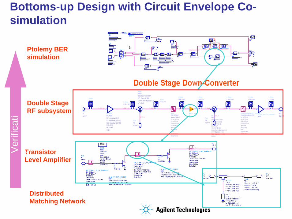
Bottoms-up Design with Circuit Envelope Co-simulation
Double Stage RF subsystem
Transistor Level Amplifier
Distributed Matching Network
Ptolemy BER simulation
Ver
ifica
tion
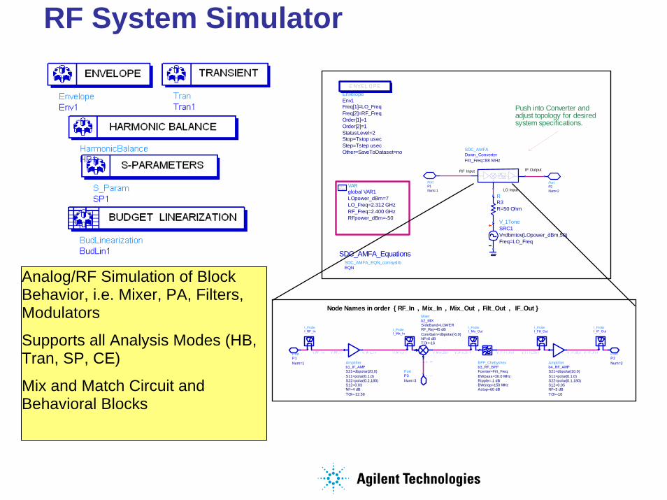
RF System Simulator
Node Names in order { RF_In , Mix_In , Mix_Out , Filt_Out , IF_Out }
PortP3Num=3
PortP1Num=1
PortP2Num=2
I_ProbeI_RF_In
Amplifierb1_IF_AMPS21=dbpolar(20,0)S11=polar(0.1,0)S22=polar(0.2,180)S12=0.03NF=4 dBTOI=-12.56
I_ProbeI_Mix_In
Mixerb2_MIXSideBand=LOWERRF_Rej=45 dBConvGain=dbpolar(-6,0)NF=6 dBTOI=-16
BPF_Chebyshevb3_RF_BPFFcenter=Filt_FreqBWpass=30.0 MHzRipple=.1 dBBWstop=150 MHzAstop=60 dB
I_ProbeI_Mix_Out
I_ProbeI_Filt_Out
Amplifierb4_RF_AMPS21=dbpolar(10,0)S11=polar(0.1,0)S22=polar(0.1,180)S12=0.05NF=3 dBTOI=-10
I_ProbeI_IF_Out
Push into Converter and adjust topology for desired system specifications.
PortP1Num=1
PortP2Num=2
VARglobal VAR1LOpower_dBm=7LO_Freq=2.312 GHzRF_Freq=2.400 GHzRFpower_dBm=-50
V_1ToneSRC1V=dbmtov(LOpower_dBm,50)Freq=LO_Freq
RR3R=50 Ohm
SDC_AMFADown_ConverterFilt_Freq=88 MHz
LO Input
IF OutputRF Input
EnvelopeEnv1Freq[1]=LO_FreqFreq[2]=RF_FreqOrder[1]=1Order[2]=1StatusLevel=2Stop=Tstop usecStep=Tstep usecOther=SaveToDataset=no
SDC_AMFA_EQN_comsyslibEQN
SDC_AMFA_Equations
Analog/RF Simulation of Block Behavior, i.e. Mixer, PA, Filters, Modulators
Supports all Analysis Modes (HB, Tran, SP, CE)
Mix and Match Circuit and Behavioral Blocks
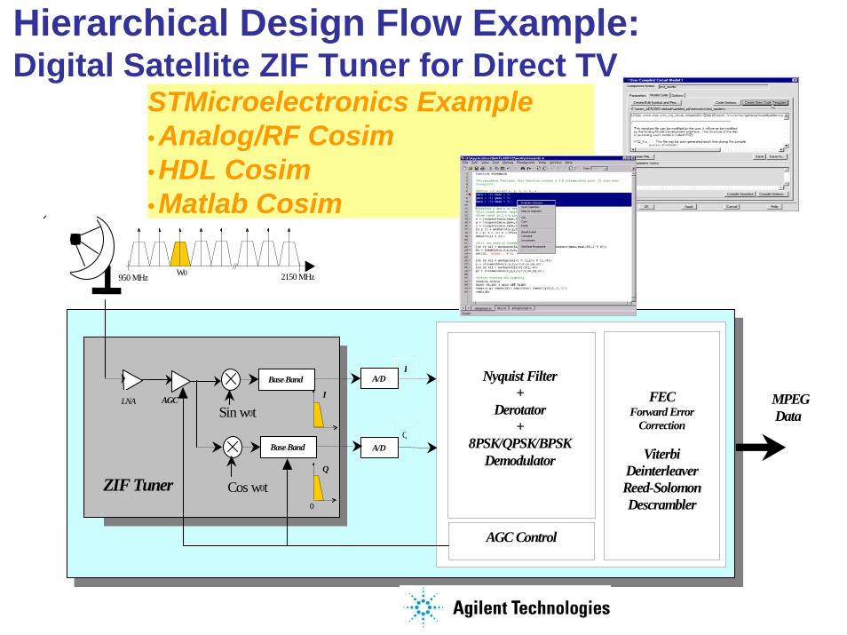
Hierarchical Design Flow Example:Digital Satellite ZIF Tuner for Direct TV
MPEG Data
I
Q
A/D
A/D
AGC Control
Nyquist Filter+
Derotator+
8PSK/QPSK/BPSKDemodulator
FECForward Error
Correction
ViterbiDeinterleaverReed-SolomonDescrambler
LNA AGC
Base-Band
Base-Band
Cos w0t
Sin w0t
950 MHz W0 2150 MHz
0
LNA
ZIF Tuner
I
Q
STMicroelectronics Example •Analog/RF Cosim•HDL Cosim•Matlab Cosim
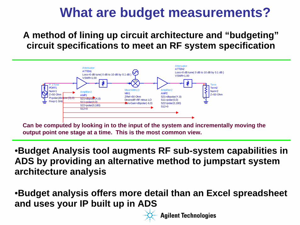
What are budget measurements?A method of lining up circuit architecture and “budgeting”circuit specifications to meet an RF system specification
AttenuatorATTEN2
VSWR=1.00Loss=0 dB tune{ 0 dB to 10 dB by 0.1 dB }
AttenuatorATTEN1
VSWR=1.00Loss=0 dB tune{ 0 dB to 10 dB by 0.1 dB }
P_1TonePORT1
Freq=1 GHzP=polar(dbmtow (0),0)Z=50 OhmNum=1
TermTerm2
Z=50 OhmNum=2MixerWithLO
MIX1
ConvGain=dbpolar(-6,0)DesiredIF=RF minus LOZRef=50 Ohm
Amplif ier2AMP1
S12=0S22=polar(0,180)S11=polar(0,0)S21=dbpolar(X,0)
Amplif ier2AMP2
S12=0S22=polar(0,180)S11=polar(0,0)S21=dbpolar(Y,0)
Can be computed by looking in to the input of the system and incrementally moving the output point one stage at a time. This is the most common view.
•Budget Analysis tool augments RF sub-system capabilities in ADS by providing an alternative method to jumpstart system architecture analysis
•Budget analysis offers more detail than an Excel spreadsheet and uses your IP built up in ADS
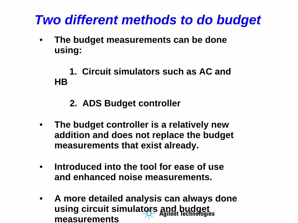
Two different methods to do budget• The budget measurements can be done
using:
1. Circuit simulators such as AC and HB
2. ADS Budget controller
• The budget controller is a relatively new addition and does not replace the budget measurements that exist already.
• Introduced into the tool for ease of use and enhanced noise measurements.
• A more detailed analysis can always done using circuit simulators and budget measurements

Don’t confuse me with two different budget analysis tools
Just tell me when do I use what?Simple!
Ready made easy to use
Quick way of getting startedNew Budget analysis tool:
Existing budget analysis tool:
More flexible
More capable
More detail
Ok that is Easy!
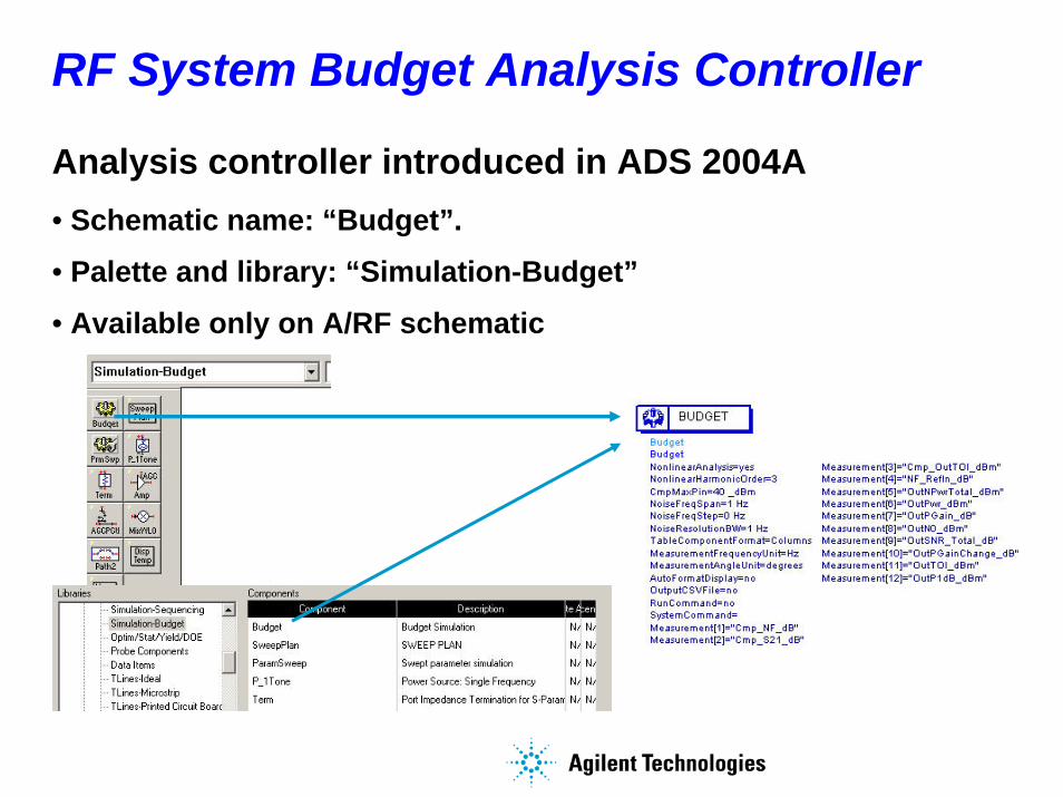
RF System Budget Analysis Controller
Analysis controller introduced in ADS 2004A• Schematic name: “Budget”.
• Palette and library: “Simulation-Budget”
• Available only on A/RF schematic
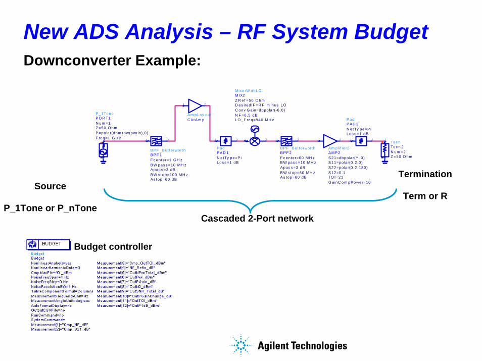
New ADS Analysis – RF System BudgetDownconverter Example:
Termination
Term or R
Cascaded 2-Port network
Source
P_1Tone or P_nTone
1 2
Am pLay outC k tA m p
1 2
Mix erW ithLOMIX2
LO _F req=940 MH zN F =6.5 dBC onv G ain=dbpolar(-6 ,0)D es iredIF =R F m inus LOZ R ef =50 O hm
1
1
2
TermTerm 2
Z =50 O hmN um =2
21
P adP AD 2
Los s =1 dBN etTy pe=P i
1
1
2
P_1TonePO R T1
F req=1 G H zP=polar(dbm tow(pwrin),0)Z =50 O hmN um =1
21
BPF _But terworthBP F 1
As top=60 dBBW s top=100 MH zApas s =3 dBBW pas s =10 MH zF c enter=1 G H z
21
PadPAD 1
Los s =1 dBN etTy pe=P i
21
B PF _But terworthB PF 2
A s top=60 dBB W s top=60 MH zA pas s =3 dBB W pas s =10 MH zF c enter=60 MH z
1 2
Am plif ie r2AMP 2
G ainC om pPower=10TO I=21S12=0.1S22=polar(0 .2 ,180)S11=polar(0 .2 ,0)S21=dbpolar(Y ,0)
Budget controller
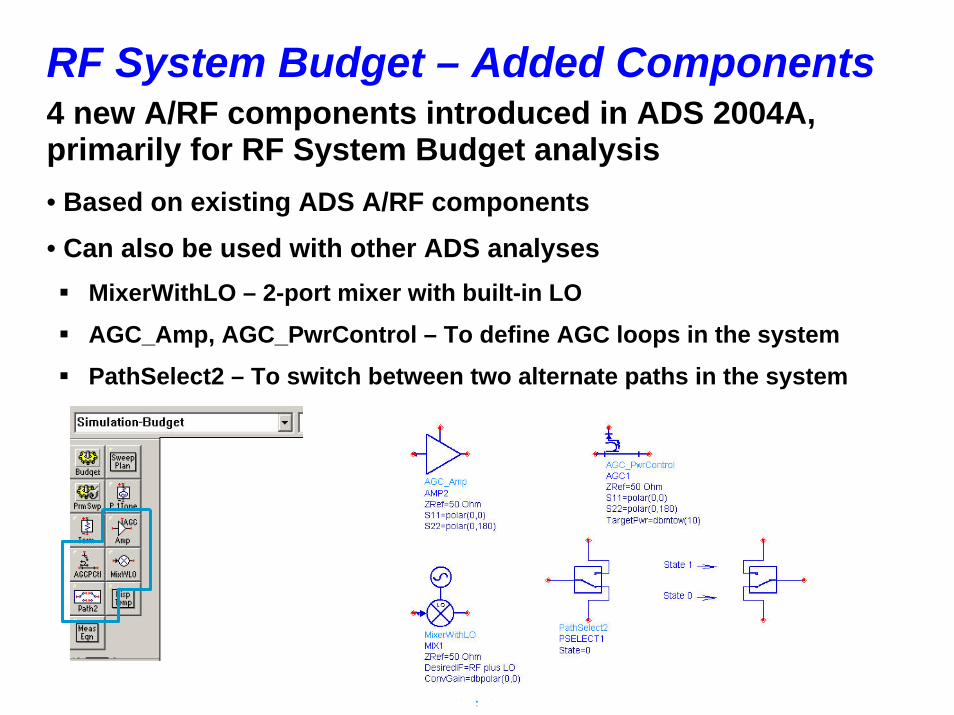
RF System Budget – Added Components4 new A/RF components introduced in ADS 2004A, primarily for RF System Budget analysis• Based on existing ADS A/RF components
• Can also be used with other ADS analysesMixerWithLO – 2-port mixer with built-in LO
AGC_Amp, AGC_PwrControl – To define AGC loops in the system
PathSelect2 – To switch between two alternate paths in the system
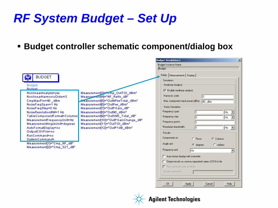
RF System Budget – Set Up
Budget controller schematic component/dialog box
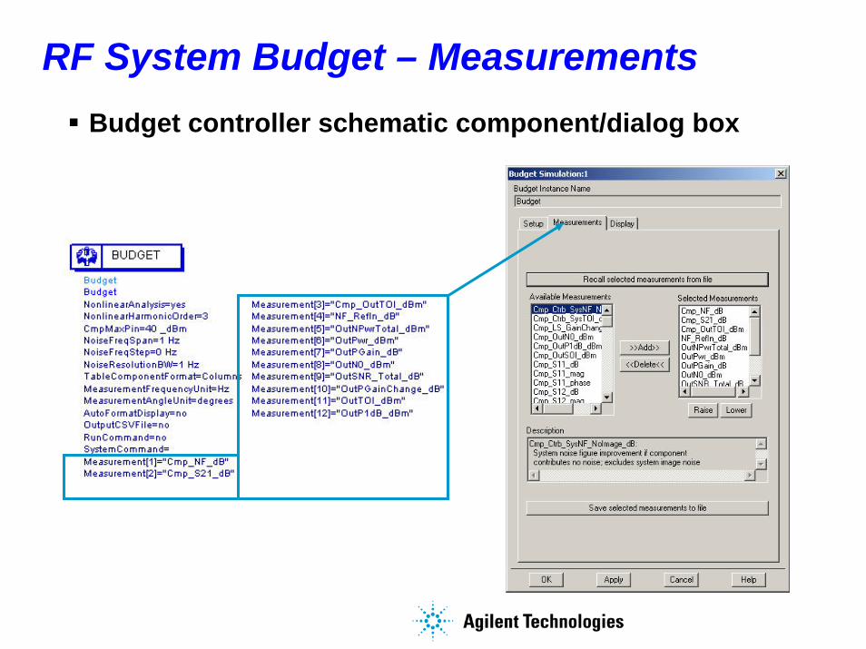
RF System Budget – MeasurementsBudget controller schematic component/dialog box
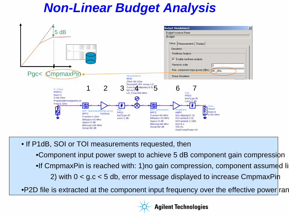
Non-Linear Budget Analysis
• If P1dB, SOI or TOI measurements requested, then•Component input power swept to achieve 5 dB component gain compression•If CmpmaxPin is reached with: 1)no gain compression, component assumed lin
2) with 0 < g.c < 5 db, error message displayed to increase CmpmaxPin
•P2D file is extracted at the component input frequency over the effective power rang
1 2 3 4 5 6 7
Pgc< CmpmaxPin
5 dB
1 2
AmpLay outCktAmp
1 2
MixerWithLOMIX2
LO_Freq=940 MHzNF=6.5 dBConv Gain=dbpolar(-6,0)DesiredIF=RF minus LOZRef =50 Ohm
1
1
2
TermTerm2
Z=50 OhmNum=2
21
PadPAD2
Loss=1 dBNetTy pe=Pi
1
1
2
P_1TonePORT1
Freq=1 GHzP=polar(dbmtow(pwrin),0)Z=50 OhmNum=1
21
BPF_ButterworthBPF1
Astop=60 dBBWstop=100 MHzApass=3 dBBWpass=10 MHzFcenter=1 GHz
21
PadPAD1
Loss=1 dBNetTy pe=Pi
21
BPF_ButterworthBPF2
Astop=60 dBBWstop=60 MHzApass=3 dBBWpass=10 MHzFcenter=60 MHz
1 2
Amplif ier2AMP2
GainCompPower=10TOI=21S12=0.1S22=polar(0.2,180)S11=polar(0.2,0)S21=dbpolar(Y ,0)
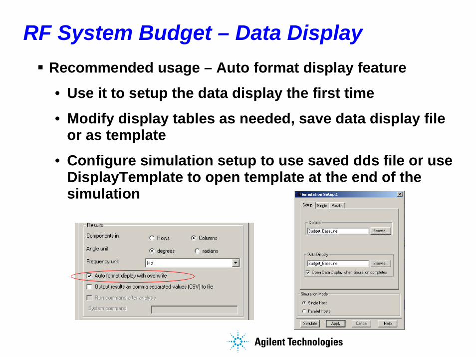
RF System Budget – Data DisplayRecommended usage – Auto format display feature
• Use it to setup the data display the first time
• Modify display tables as needed, save data display file or as template
• Configure simulation setup to use saved dds file or useDisplayTemplate to open template at the end of the simulation
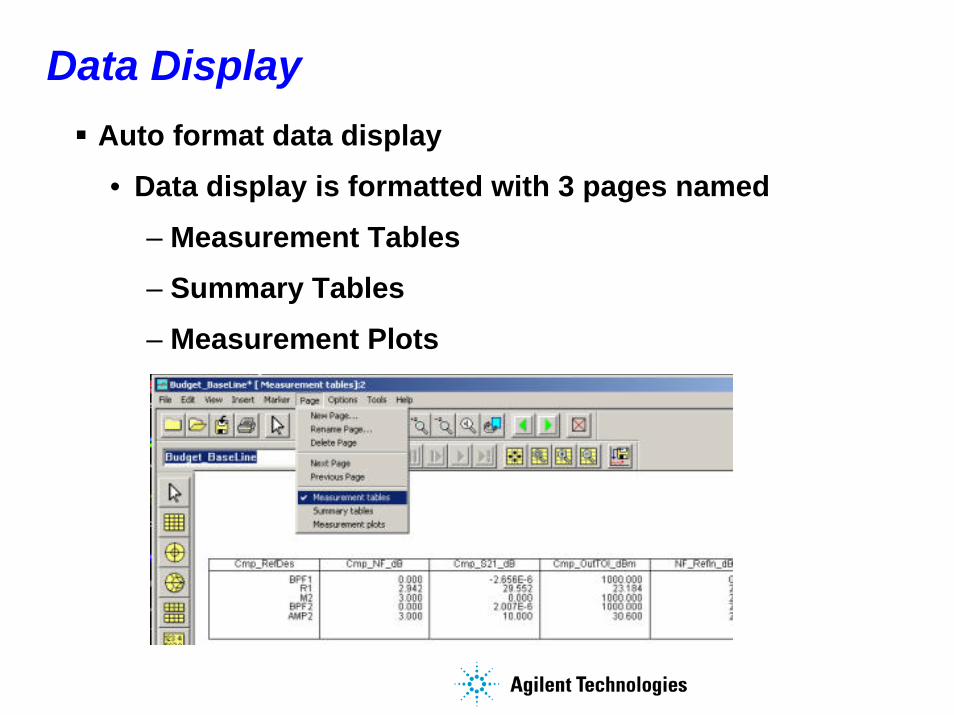
Data DisplayAuto format data display
• Data display is formatted with 3 pages named
– Measurement Tables
– Summary Tables
– Measurement Plots
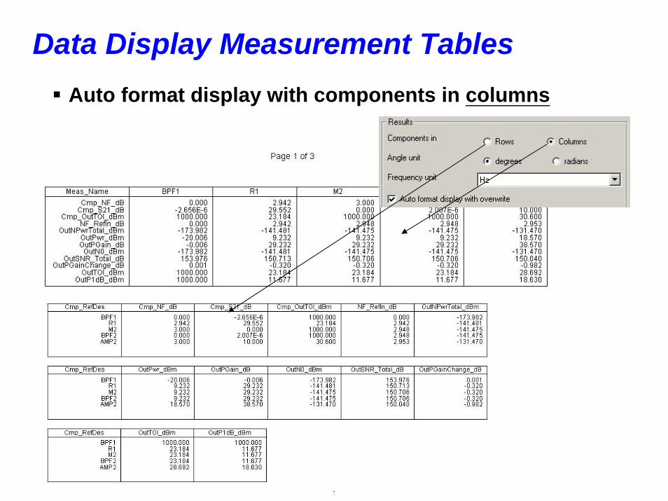
Data Display Measurement TablesAuto format display with components in columns
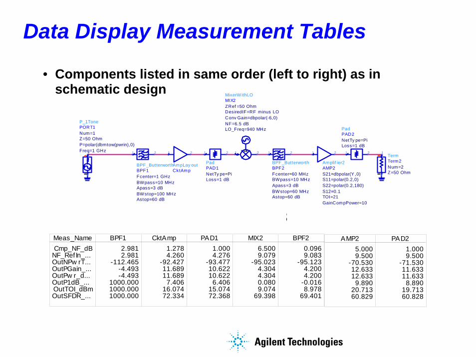
Data Display Measurement Tables
• Components listed in same order (left to right) as in schematic design
1 2
AmpLay outCktAmp
1 2
MixerWithLOMIX2
LO_Freq=940 MHzNF=6.5 dBConv Gain=dbpolar(-6,0)DesiredIF=RF minus LOZRef =50 Ohm
1
1
2
TermTerm2
Z=50 OhmNum=2
21
PadPAD2
Loss=1 dBNetTy pe=Pi
1
1
2
P_1TonePORT1
Freq=1 GHzP=polar(dbmtow(pwrin),0)Z=50 OhmNum=1
21
BPF_ButterworthBPF1
Astop=60 dBBWstop=100 MHzApass=3 dBBWpass=10 MHzFcenter=1 GHz
21
PadPAD1
Loss=1 dBNetTy pe=Pi
21
BPF_ButterworthBPF2
Astop=60 dBBWstop=60 MHzApass=3 dBBWpass=10 MHzFcenter=60 MHz
1 2
Amplif ier2AMP2
GainCompPower=10TOI=21S12=0.1S22=polar(0.2,180)S11=polar(0.2,0)S21=dbpolar(Y ,0)
Page 1 of 3Meas_NameCmp_NF_dB
NF_Ref In_...OutNPw rT...OutPGain_...OutPw r_d...OutP1dB_...OutTOI_dBmOutSFDR_...
BPF12.9812.981
-112.465-4.493-4.493
1000.0001000.0001000.000
CktAmp1.2784.260
-92.42711.68911.689
7.40616.07472.334
PAD11.0004.276
-93.47710.62210.622
6.40615.07472.368
MIX26.5009.079
-95.0234.3044.3040.0809.074
69.398
BPF20.0969.083
-95.1234.2004.200
-0.0168.978
69.401
AMP25.0009.500
-70.53012.63312.633
9.89020.71360.829
PAD21.0009.500
-71.53011.63311.633
8.89019.71360.828
Data Display Summary TablesAuto format display – “Summary Tables”page System_Name
SystemInN0_dBmSystemInNPwr_dBmSystemInP1dB_dBm
SystemInSOI_dBmSystemInTOI_dBm
SystemNF_dBSystemOutN0_dBm
SystemOutNPwr_dBmSystemOutP1dB_dBm
SystemOutSOI_dBmSystemOutTOI_dBm
SystemPGain_SS_dBSystemPGain_dB
SystemPOut_dBmSystemS11_dB
SystemS11_magSystemS11_phase
SystemS12_dBSystemS12_mag
SystemS12_phaseSystemS21_dB
SystemS21_magSystemS21_phase
SystemS22_dBSystemS22_mag
SystemS22_phase
System_Value
-173.855-107.834
-20.0311000.000
-10.2089.500
-134.540-71.530
8.8901000.000
19.71329.92111.63311.633
-11.2800.273
-149.565-400.000
0.0000.000
11.6333.816
119.390-14.115
0.197177.656
Setup_Name
System_AnalysisTypeSystem_NoiseResBWSystem_NoiseSimBW
System_NoiseSimFStepSystem_PilotFreq
System_PilotPwr_dBmSystem_RefR
System_SourceFreqSystem_SourcePwr_dBm
System_SourceTemp
Setup_Value
1.0001.000
2.000E62.000E61.000E9
-5.786E-1550.000
1.000E9-5.786E-15
25.000
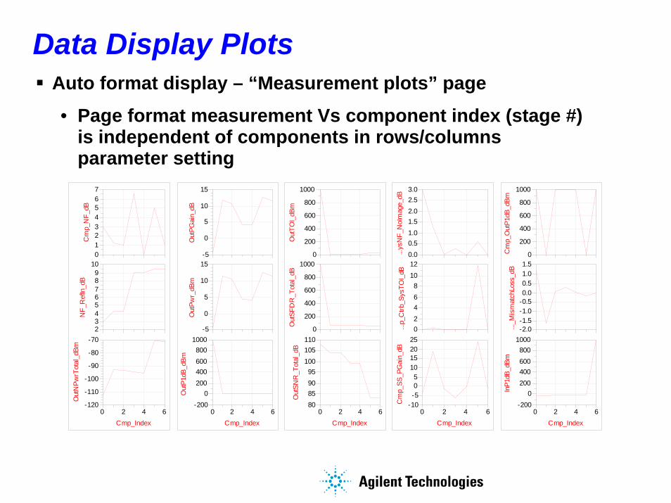
Data Display PlotsAuto format display – “Measurement plots” page
• Page format measurement Vs component index (stage #) is independent of components in rows/columns parameter setting
123456
0
7
Cm
p_N
F_dB
3456789
2
10
NF_
Ref
In_d
B
2 40 6
-110
-100
-90
-80
-120
-70
Cmp_Index
Out
NPw
rTot
al_d
Bm
0
5
10
-5
15O
utPG
ain_
dB
0
5
10
-5
15
Out
Pwr_
dBm
2 40 6
0200400600800
-200
1000
Cmp_Index
Out
P1dB
_dBm
200
400
600
800
0
1000
Out
TOI_
dBm
200
400
600
800
0
1000
Out
SFD
R_T
otal
_dB
2 40 6
859095
100105
80
110
Cmp_Index
Out
SNR
_Tot
al_d
B
0.51.01.52.02.5
0.0
3.0
...ys
NF_
NoI
mag
e_dB
2468
10
0
12
...p_
Ctrb
_Sys
TOI_
dB2 40 6
-505
101520
-10
25
Cmp_Index
Cm
p_SS
_PG
ain_
dB
200
400
600
800
0
1000
Cm
p_O
utP1
dB_d
Bm
-1.5-1.0-0.50.00.51.0
-2.0
1.5
..._M
ism
atch
Loss
_dB
2 40 6
0200400600800
-200
1000
Cmp_Index
InP1
dB_d
Bm
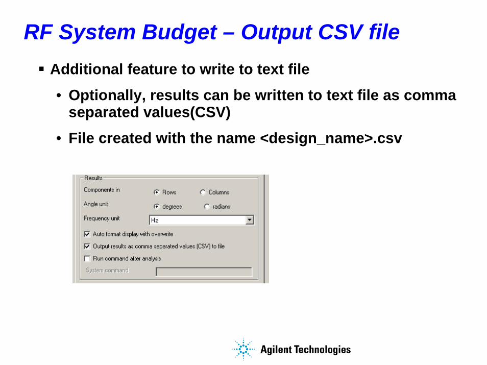
RF System Budget – Output CSV fileAdditional feature to write to text file
• Optionally, results can be written to text file as comma separated values(CSV)
• File created with the name <design_name>.csv
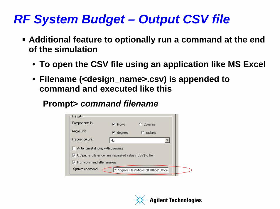
RF System Budget – Output CSV fileAdditional feature to optionally run a command at the end of the simulation
• To open the CSV file using an application like MS Excel
• Filename (<design_name>.csv) is appended to command and executed like this
Prompt> command filename
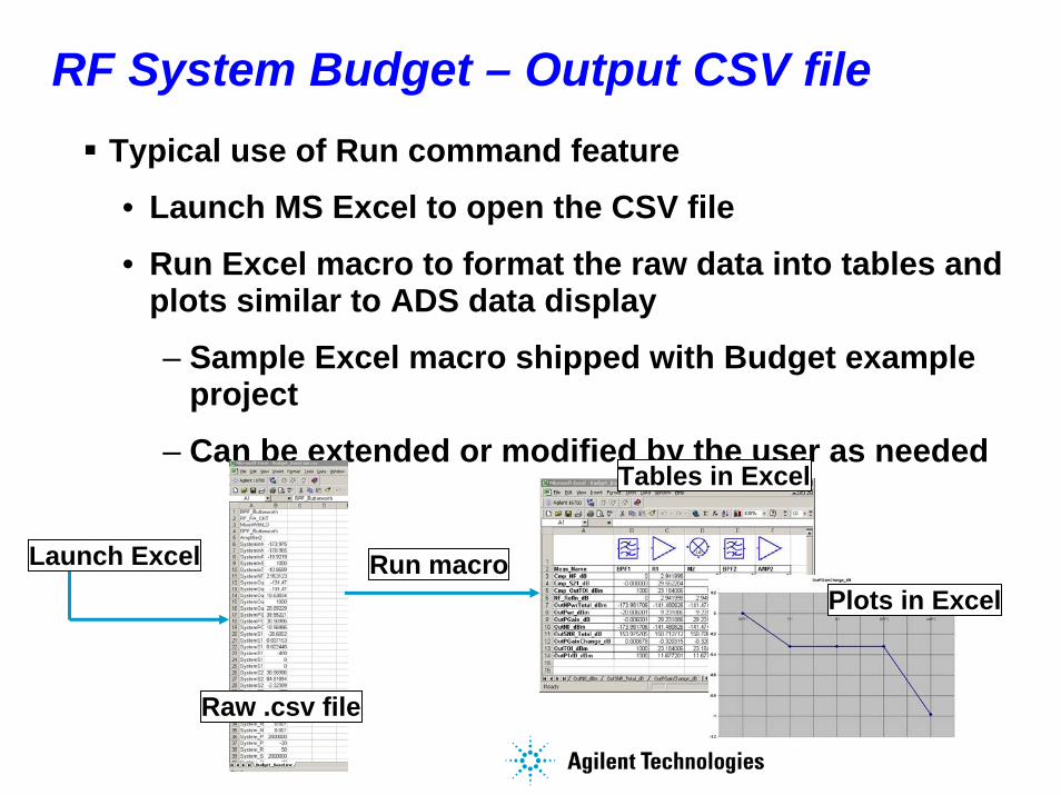
RF System Budget – Output CSV fileTypical use of Run command feature
• Launch MS Excel to open the CSV file
• Run Excel macro to format the raw data into tables and plots similar to ADS data display
– Sample Excel macro shipped with Budget example project
– Can be extended or modified by the user as needed
Launch Excel
Raw .csv file
Run macro
Tables in Excel
Plots in Excel
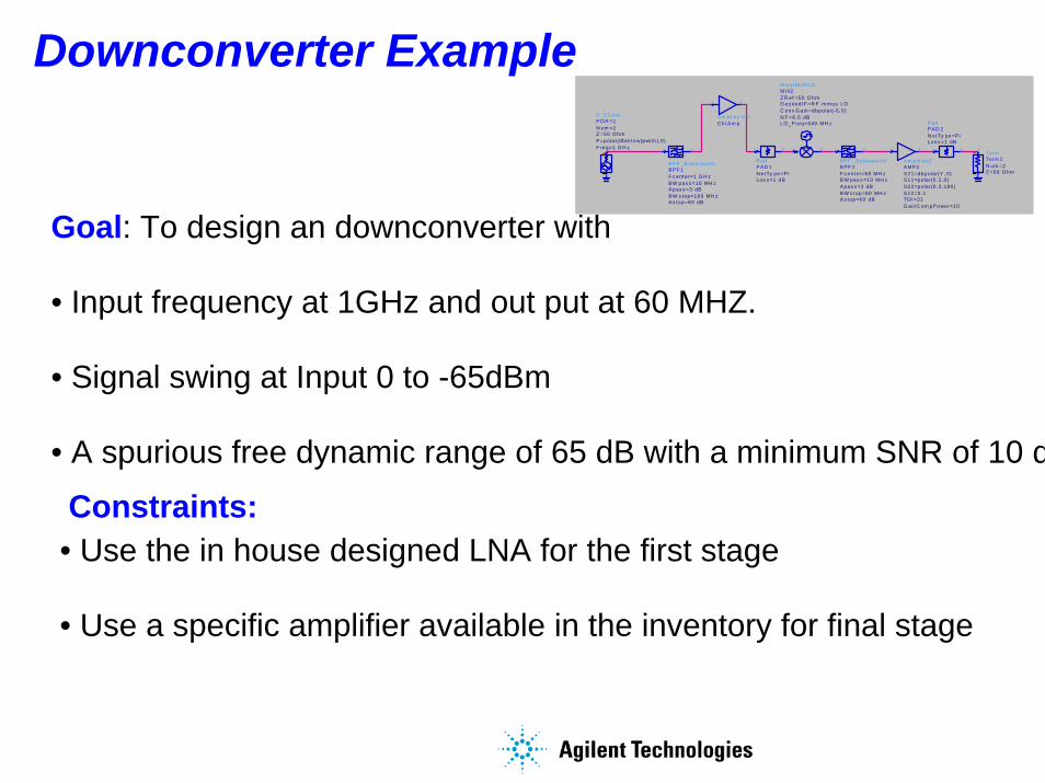
Downconverter Example
Goal: To design an downconverter with
• Input frequency at 1GHz and out put at 60 MHZ.
• Signal swing at Input 0 to -65dBm
• A spurious free dynamic range of 65 dB with a minimum SNR of 10 d
1 2
Am pLay outC k tAm p
1 2
Mix erW ithLOMIX2
LO _F req=940 MH zN F =6.5 dBC onv G ain=dbpolar(-6,0 )D es iredIF =R F m inus LOZ R ef =50 O hm
1
1
2
TermTerm 2
Z =50 O hmN um =2
21
PadPAD 2
Los s =1 dBN etTy pe=P i
1
1
2
P_1TonePO R T1
F req=1 G H zP=polar(dbm tow(pwrin ),0)Z =50 O hmN um =1
21
BPF _But terworthBPF 1
As top=60 dBBW s top=100 MH zApas s =3 dBBW pas s =10 MH zF c enter=1 G H z
21
PadPAD 1
Los s =1 dBN etTy pe=P i
21
BPF _But te rworthBPF 2
As top=60 dBBW s top=60 MH zApas s =3 dBBW pas s =10 MH zF c enter=60 MH z
1 2
Am plif ie r2AMP2
G ainC om pPower=10TO I=21S12=0.1S22=polar(0 .2,180)S11=polar(0 .2,0)S21=dbpolar(Y ,0)
Constraints:• Use the in house designed LNA for the first stage
• Use a specific amplifier available in the inventory for final stage
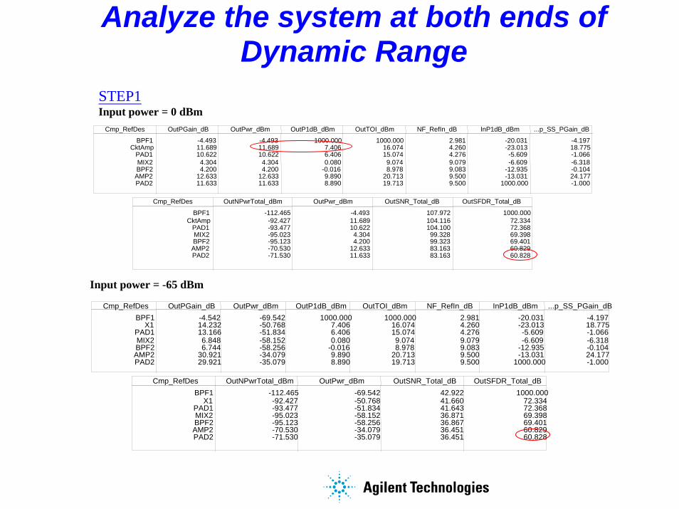
Analyze the system at both ends ofDynamic Range
STEP1Input power = 0 dBm
Cmp_RefDes
BPF1CktAmp
PAD1MIX2BPF2AMP2PAD2
OutPGain_dB
-4.49311.68910.6224.3044.200
12.63311.633
OutPwr_dBm
-4.49311.68910.6224.3044.200
12.63311.633
OutP1dB_dBm
1000.0007.4066.4060.080
-0.0169.8908.890
OutTOI_dBm
1000.00016.07415.0749.0748.978
20.71319.713
NF_RefIn_dB
2.9814.2604.2769.0799.0839.5009.500
InP1dB_dBm
-20.031-23.013-5.609-6.609
-12.935-13.031
1000.000
...p_SS_PGain_dB
-4.19718.775-1.066-6.318-0.10424.177-1.000
Cmp_RefDes
BPF1CktAmp
PAD1MIX2BPF2AMP2PAD2
OutNPwrTotal_dBm
-112.465-92.427-93.477-95.023-95.123-70.530-71.530
OutPwr_dBm
-4.49311.68910.6224.3044.200
12.63311.633
OutSNR_Total_dB
107.972104.116104.10099.32899.32383.16383.163
OutSFDR_Total_dB
1000.00072.33472.36869.39869.40160.82960.828
Input power = -65 dBm
Cmp_RefDesBPF1
X1PAD1MIX2BPF2AMP2PAD2
OutPGain_dB-4.54214.23213.1666.8486.744
30.92129.921
OutPwr_dBm-69.542-50.768-51.834-58.152-58.256-34.079-35.079
OutP1dB_dBm1000.000
7.4066.4060.080
-0.0169.8908.890
OutTOI_dBm1000.000
16.07415.0749.0748.978
20.71319.713
NF_RefIn_dB2.9814.2604.2769.0799.0839.5009.500
InP1dB_dBm-20.031-23.013-5.609-6.609
-12.935-13.031
1000.000
...p_SS_PGain_dB-4.19718.775-1.066-6.318-0.10424.177-1.000
Cmp_RefDesBPF1
X1PAD1MIX2BPF2AMP2PAD2
OutNPwrTotal_dBm-112.465-92.427-93.477-95.023-95.123-70.530-71.530
OutPwr_dBm-69.542-50.768-51.834-58.152-58.256-34.079-35.079
OutSNR_Total_dB42.92241.66041.64336.87136.86736.45136.451
OutSFDR_Total_dB1000.000
72.33472.36869.39869.40160.82960.828
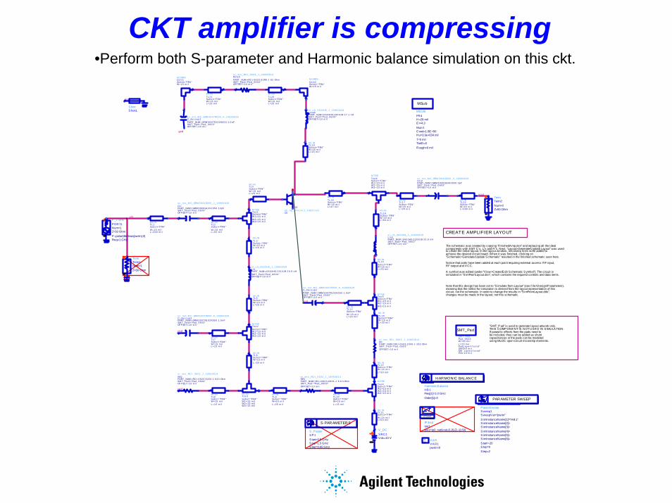
CKT amplifier is compressing
vin
vout
CREATE AMPLIFIER LAYOUT
"SMT_Pad" is used to generate layout artwork only.THIS COMPONENT IS NOT USED IN S IMULATION.If parasitic effects from the pads need tobe included, they can be added as shunt capacitances or the pads can be modeledusing MLOC open-circuit microstrip elements.
The schematic was created by copying "FinishedA mp.dsn" and replacing all the idealcomponents with SMT C's, L's and R's. Next, "Layout>Generate/Update Layout" was usedto create the initial layout. In the layout window, microstrip lines were added toachieve the desired circuit board. When it was finished, clicking on "Schematic>Generate/Update Schematic" resulted in the finished schematic seen here.
Notice that ports have been added at each point requiring external access: RF input, RF output and V CC.
A symbol was edited (under "V iew>Create/E dit S chematic S ymbol"). The circuit issimulated in "S imFromLayout.dsn", which contains the required controls and data items.
Note that this design has been set to "S imulate from Layout" (see File>Design/Parameters),meaning that the netlist for simulation is derived from the layout representation of thiscircuit, not the schematic. In order to change the results in "S imFromLayout.dds",changes must be made in the layout, not this schematic.
S _ParamS P1
S tep=0.05 GHzS top=1.5 GHzS tart=0.5 GHz
S-PAR AMETER S IP3outipo1ipo1=ip3_out(vout,{1,0},{2,-1},50)
P 0
P in
IP3 o u t
V ARV AR1pwrin=0
EqnVar
P aramSweepS weep1
S tep=2S top=0S tart=-20S imInstanceName[6]=S imInstanceName[5]=S imInstanceName[4]=S imInstanceName[3]=S imInstanceName[2]=S imInstanceName[1]="HB1"S weepVar="pwrin"
PARAMETER SWEEP
HarmonicB alanceHB1
Order[1]=3Freq[1]=1.0 GHz
H ARMON IC BALANC E
TermTerm1
Z=50 OhmNum=1
P_1TonePORT1
Freq=1 GHzP=polar(dbmtow(pwrin),0)Z=50 OhmNum=1
TermTerm2
Z=50 OhmNum=2
V_DCSRC1Vdc=10 V
MSUBFR4
Rough=0 milTanD=0T=0 milHu=3.9e+034 milCond=1.0E +50Mur=1E r=4.3H=28 mil
MSub
gnd
s r_ im s _ RC-I_ 0 6 0 3 _ J _ 1 9 9 5 0 8 1 4RB2PART_ NUM =RC-I-0 6 0 3 -6 2 0 0 -J 6 2 0 Oh mSM T_ Pa d ="Pa d _ 0 6 0 3 "OFFSET= 1 0 m i l
gnd
s c _ m rt_ M C_ GRM 3 9 X7 R0 5 0 _ K_ 1 9 9 6 0 8 2 8C_ d e c o u p 2
OFFSET=1 0 m i lSM T_ Pa d ="Pa d _ 0 6 0 3 "PART_ NUM = GRM 3 9 X7 R1 0 2 K0 5 0 1 .0 n F
gndp b _ h p _ AT4 1 4 1 1 _ 1 9 9 2 1 1 0 1Q1
gnd
s c _ m rt_ M C_ GRM 3 9 X7 R0 5 0 _ K_ 1 9 9 6 0 8 2 8C_ d e c o u p 1
OFFSET=1 0 m i lSM T_ Pa d ="Pa d _ 0 6 0 3 "PART_ NUM =GRM 3 9 X7 R1 0 2 K0 5 0 1 .0 n F
gnd
s c _ m rt_ M C_ GRM 3 9 X7 R0 5 0 _ K_ 1 9 9 6 0 8 2 8C_ d e c o u p 3
OFFSET= 1 0 m i lSM T_ Pa d ="Pa d _ 0 6 0 3 "PART_ NUM =GRM 3 9 X7 R1 0 2 K0 5 0 1 .0 n F
gnd
ShortShort1
SM T_ Pa dPa d _ 0 6 0 3
PO=-1 0 m i lSM _ L a y e r="c o n d "SM O=0 m i lPa d L a y e r="c o n d "L =2 0 m i lW =3 0 m i l
SMT_Pad
M L INTL 1
L = 2 0 0 m i lW= 1 5 m i lSu b s t="FR4 "
M L INTL 2
L =5 0 m i lW=1 5 m i lSu b s t="FR4 "
M TEETe e 1Su b s t= "FR4 "W 1 =1 5 m i lW 2 =1 5 m i lW 3 =1 5 m i l
M L INTL 3
L =1 5 m i lW=1 5 m i lSu b s t="FR4 "
s l_ c ft_ 0 6 0 3 HS_ J _ 1 9 9 6 0 8 2 8L inPART_ NUM =0 6 0 3 HS-2 2 0 XJ B 2 0 .9 n HSM T_ Pa d ="Pa d _ 0 6 0 3 "OFFSET=1 0 m i l
M L INTL 6
L =5 0 m i lW=1 5 m i lSu b s t="FR4 "
M TEETe e 2Su b s t= "FR4 "W 1 =1 5 m i lW 2 =1 5 m i lW 3 =1 5 m i l
M L INTL 5
L =2 5 m i lW=1 5 m i lSu b s t="FR4 "
M L INTL 7
L =1 5 m i lW=1 5 m i lSu b s t="FR4 "
M L INTL 8
L =1 5 m i lW=1 5 m i lSu b s t="FR4 "
M TEETe e 3Su b s t="FR4 "W1 =1 5 m i lW2 =1 5 m i lW3 =1 5 m i l
M L INTL 9
L =2 5 m i lW =1 5 m i lSu b s t= "FR4 "
M L INTL 1 0
L =1 5 m i lW=1 5 m i lSu b s t="FR4 "
M L INTL 2 0
L =2 5 m i lW=1 5 m i lSu b s t="FR4 "
M L INTL 2 1
L =2 5 m i lW= 1 5 m i lSu b s t="FR4 "
s l_ c ft_ 0 6 0 3 HS_ J _ 1 9 9 6 0 8 2 8L s ta bPART_ NUM =0 6 0 3 HS-1 8 0 XJ B 1 7 .1 n HSM T_ Pa d ="Pa d _ 0 6 0 3 "OFFSET=1 0 m i l
M L INTL 1 9
L =1 5 m i lW =1 5 m i lSu b s t= "FR4 "
M TEETe e 4Su b s t="FR4 "W1 =1 5 m i lW2 =1 5 m i lW3 =1 5 m i l
M L INTL 1 1
L =5 0 m i lW= 1 5 m i lSu b s t="FR4 "
M L INTL 1 2
L =3 0 m i lW= 1 5 m i lSu b s t="FR4 "
s r_ im s _ RC-I_ 0 6 0 3 _ J _ 1 9 9 5 0 8 1 4RCPART_ NUM =RC-I-0 6 0 3 -2 0 0 0 -J 2 0 0 Oh mSM T_ Pa d ="Pa d _ 0 6 0 3 "OFFSET=1 0 m i l
M L INTL 1 5
L = 3 0 m i lW= 1 5 m i lSu b s t="FR4 "
M TEETe e 5Su b s t="FR4 "W1 =1 5 m i lW2 =1 5 m i lW3 =1 5 m i lM L IN
TL 1 4
L =1 5 m i lW=1 5 m i lSu b s t="FR4 "
M L INTL 1 3
L =2 5 m i lW= 1 5 m i lSu b s t="FR4 "
M L INTL 1 7
L =2 5 m i lW= 1 5 m i lSu b s t="FR4 "
M L INTL 2 2
L =2 0 0 m i lW=1 5 m i lSu b s t="FR4 "
M L INTL 1 6
L =3 7 m i lW= 1 5 m i lSu b s t="FR4 "
s c _ m rt_ M C_ GRM 3 9 C0 G0 5 0 _ C_ 1 9 9 6 0 8 2 8Co u t
OFFSET=1 0 m i lSM T_ Pa d ="Pa d _ 0 6 0 3 "PART_ NUM = GRM 3 9 C0 G0 3 0 C0 5 0 3 p F
M TEETe e 6Su b s t="FR4 "W1 =1 5 m i lW2 =1 5 m i lW3 =1 5 m i l
s l_ c ft_ 0 6 0 3 HS_ J _ 1 9 9 6 0 8 2 8L o u tPART_ NUM = 0 6 0 3 HS-2 2 0 XJ B 2 0 .9 n HSM T_ Pa d ="Pa d _ 0 6 0 3 "OFFSET=1 0 m i l
M L INTL 1 8
L =5 0 m i lW =1 5 m i lSu b s t= "FR4 "
M CORNCo rn 1Su b s t="FR4 "W=1 5 m i l
s r_ im s _ RC-I_ 0 6 0 3 _ J _ 1 9 9 5 0 8 1 4Rs ta bPART_ NUM =RC-I-0 6 0 3 -8 2 R0 -J 8 2 Oh mSM T_ Pa d = "Pa d _ 0 6 0 3 "OFFSET=1 0 m i l
M CORNCo rn 2Su b s t= "FR4 "W =1 5 m i l
s c _ m rt_ M C_ GRM 3 9 C0 G0 5 0 _ J _ 1 9 9 6 0 8 2 8Cin
OFFSET= 1 0 m i lSM T_ Pa d ="Pa d _ 0 6 0 3 "PART_ NUM =GRM 3 9 C0 G1 2 0 J 0 5 0 1 2 p F
M L INTL 4
L =2 5 m i lW= 1 5 m i lSu b s t="FR4 "
s r_ im s _ RC-I_ 0 6 0 3 _ J _ 1 9 9 5 0 8 1 4RB1PART_ NUM =RC-I-0 6 0 3 -6 8 0 1 -J 6 .8 k Oh mSM T_ Pa d ="Pa d _ 0 6 0 3 "OFFSET=1 0 m i l
•Perform both S-parameter and Harmonic balance simulation on this ckt.
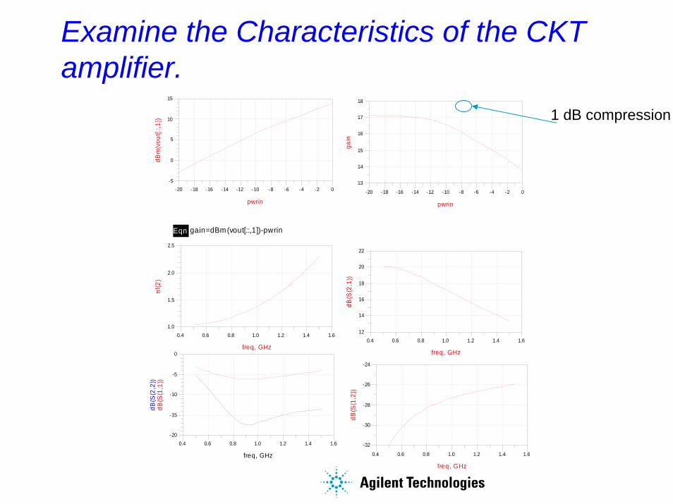
Examine the Characteristics of the CKT amplifier.
-18 -16 -14 -12 -10 -8 -6 -4 -2-20 0
0
5
10
-5
15
pwrin
dBm
(vou
t[::,1
])
Eqn gain=dBm (vout[::,1])-pwrin
-18 -16 -14 -12 -10 -8 -6 -4 -2-20 0
14
15
16
17
13
18
pwrin
gain
0.6 0.8 1.0 1.2 1.40.4 1.6
1.5
2.0
1.0
2.5
freq, GHz
nf(2
)
0.6 0.8 1.0 1.2 1.40.4 1.6
14
16
18
20
12
22
freq, GHzdB
(S(2
,1))
0.6 0.8 1.0 1.2 1.40.4 1.6
-15
-10
-5
-20
0
freq, GHz
dB(S
(1,1
))dB
(S(2
,2))
0.6 0.8 1.0 1.2 1.40.4 1.6
-30
-28
-26
-32
-24
freq, GHz
dB(S
(1,2
))
1 dB compression
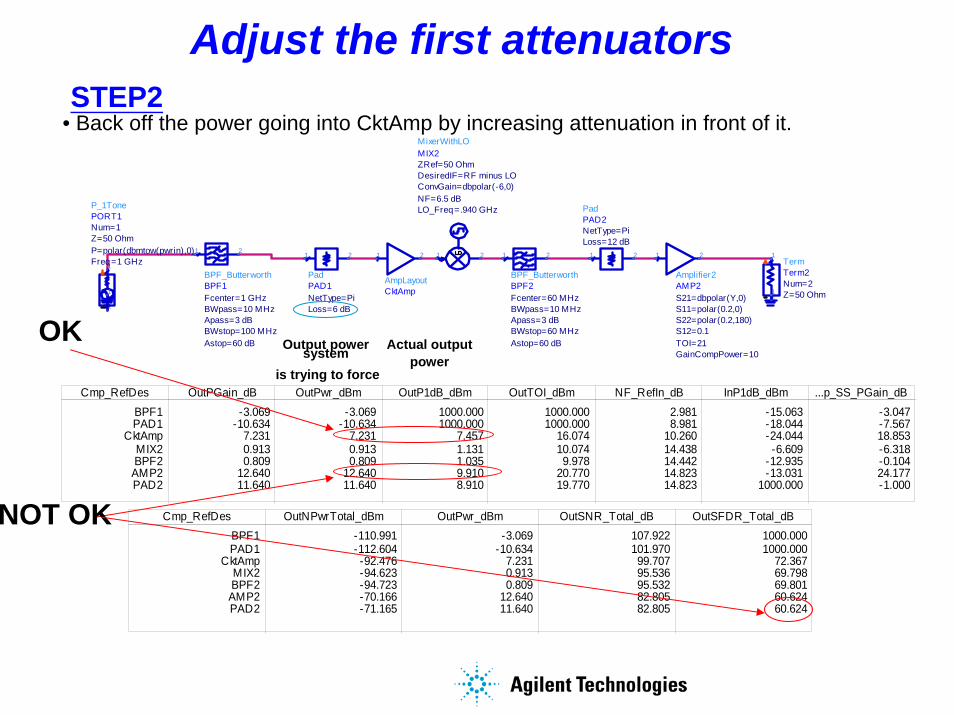
Adjust the first attenuatorsSTEP2
1
2
P_1TonePORT1
Freq=1 GHzP=polar(dbmtow(pwrin),0)Z=50 OhmNum=1
1
21
BPF_ButterworthBPF1
Astop=60 dBBWstop=100 MHzApass=3 dBBWpass=10 MHzFcenter=1 GHz
21
PadPAD1
Loss=6 dBNetType=Pi
21
PadPAD2
Loss=12 dBNetType=Pi
1 2
MixerWithLOMIX2
LO_Freq=.940 GHzNF=6.5 dBConvGain=dbpolar(-6,0)DesiredIF=RF minus LOZRef=50 Ohm
1
1
2
TermTerm2
Z=50 OhmNum=2
1 2
Amplifier2AMP2
GainCompPower=10TOI=21S12=0.1S22=polar(0.2,180)S11=polar(0.2,0)S21=dbpolar(Y,0)
1 2
AmpLayoutCktAmp
21
BPF_ButterworthBPF2
Astop=60 dBBWstop=60 MHzApass=3 dBBWpass=10 MHzFcenter=60 MHz
Cmp_RefDesBPF1PAD1
CktAmpMIX2BPF2AMP2PAD2
OutPGain_dB-3.069
-10.6347.2310.9130.809
12.64011.640
OutPwr_dBm-3.069
-10.6347.2310.9130.809
12.64011.640
OutP1dB_dBm1000.0001000.000
7.4571.1311.0359.9108.910
OutTOI_dBm1000.0001000.000
16.07410.0749.978
20.77019.770
NF_RefIn_dB2.9818.981
10.26014.43814.44214.82314.823
InP1dB_dBm-15.063-18.044-24.044-6.609
-12.935-13.031
1000.000
...p_SS_PGain_dB-3.047-7.56718.853-6.318-0.10424.177-1.000
Cmp_RefDesBPF1PAD1
CktAmpMIX2BPF2AMP2PAD2
OutNPwrTotal_dBm-110.991-112.604-92.476-94.623-94.723-70.166-71.165
OutPwr_dBm-3.069
-10.6347.2310.9130.809
12.64011.640
OutSNR_Total_dB107.922101.97099.70795.53695.53282.80582.805
OutSFDR_Total_dB1000.0001000.000
72.36769.79869.80160.62460.624
• Back off the power going into CktAmp by increasing attenuation in front of it.
OK
NOT OK
Output power systemis trying to force
Actual output power
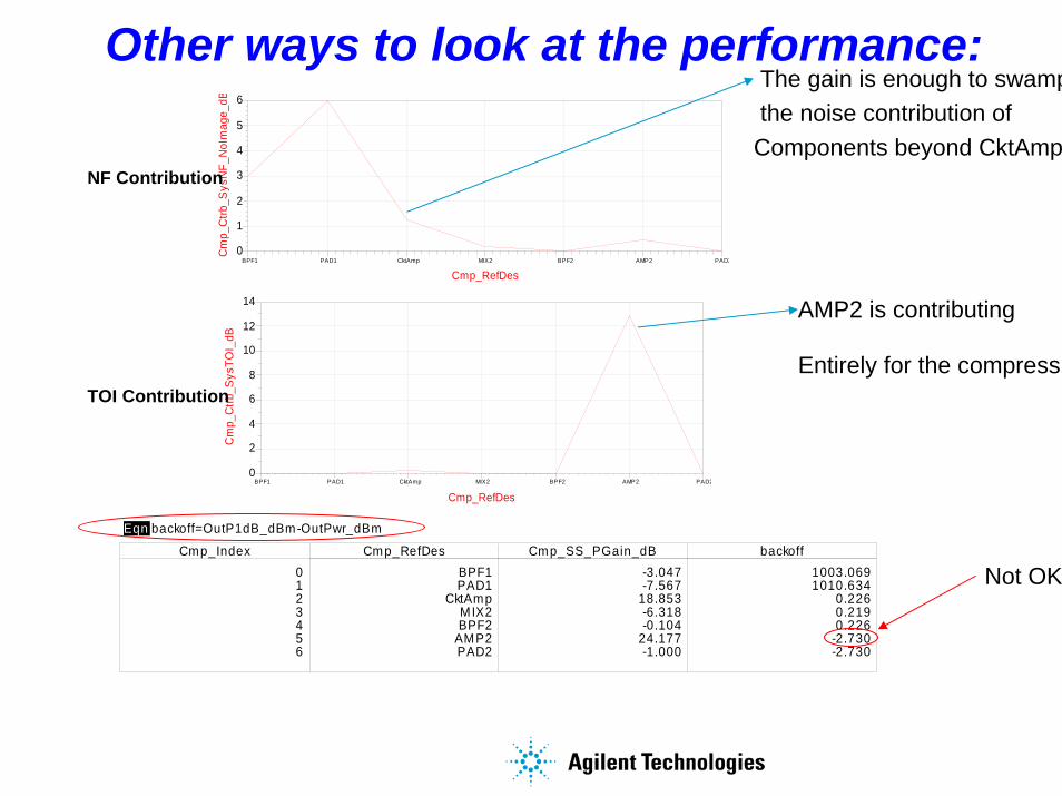
Other ways to look at the performance:
PAD1 CktAmp MIX2 BPF2 AMP2BPF1 PAD2
1
2
3
4
5
0
6
Cmp_RefDes
Cm
p_C
trb_S
ysN
F_N
oIm
age_
dB
PAD1 CktAmp MIX2 BPF2 AMP2BPF1 PAD2
2
4
6
8
10
12
0
14
Cmp_RefDes
Cm
p_C
trb_S
ysTO
I_dB
Eqn backoff=OutP1dB_dBm-OutPwr_dBm
Cmp_Index0123456
Cmp_RefDesBPF1PAD1
CktAmpMIX2BPF2
AMP2PAD2
Cmp_SS_PGain_dB-3.047-7.567
18.853-6.318-0.104
24.177-1.000
backoff1003.0691010.634
0.2260.2190.226
-2.730-2.730
The gain is enough to swampthe noise contribution of
Components beyond CktAmp
AMP2 is contributing
Entirely for the compressi
NF Contribution
TOI Contribution
Not OK
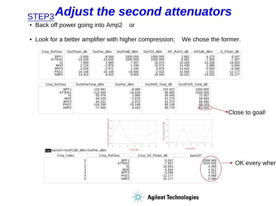
STEP3• Back off power going into Amp2 or
• Look for a better amplifier with higher compression; We chose the former.
Cmp_Ref DesBPF1
ATTEN1X1
MIX2BPF3PAD1AMP2
OutPGain_dB-3.069
-10.6397.9692.1242.028
-10.14813.423
OutPwr_dBm-8.069
-15.6392.969
-2.876-2.972
-15.1488.423
OutP1dB_dBm1000.0001000.000
7.4571.4361.340
-10.6608.903
OutTOI_dBm1000.0001000.000
16.07410.074
9.978-2.02218.442
NF_Ref In_dB2.9818.981
10.26014.43814.44216.56519.331
InP1dB_dBm-4.375-7.356
-13.3565.086
-0.935-1.031
-13.031
...S_PGain_dB-3.047-7.56718.853-5.844-0.096
-12.17724.177
Cmp_Ref DesBPF1
ATTEN1X1
MIX2BPF3PAD1AMP2
OutNPwrTotal_dBm-110.991-112.604
-92.476-94.150-94.241
-104.296-77.355
OutPwr_dBm-8.069
-15.6392.969
-2.876-2.972
-15.1488.423
OutSNR_Total_dB102.922
96.96595.44591.27491.27089.14885.778
OutSFDR_Total_dB1000.0001000.000
72.36769.48369.48068.18363.865
Eqn backof f =OutP1dB_dBm-OutPwr_dBmCmp_Index
0123456
Cmp_Ref DesBPF1
ATTEN1X1
MIX2BPF3PAD1AMP2
Cmp_SS_PGain_dB-3.047-7.56718.853-5.844-0.096
-12.17724.177
backof f1008.0691015.639
4.4884.3124.3124.4880.480
1 2 3 4 50 6
2
4
0
6
Cmp_Index
Cm
p_C
trb_S
ysN
F_N
oIm
age_
dB
1 2 3 4 50 6
1
2
3
0
4
C mp_Index
Cm
p_C
trb_S
ysTO
I_dB
Close to goal!
OK every where
Adjust the second attenuators
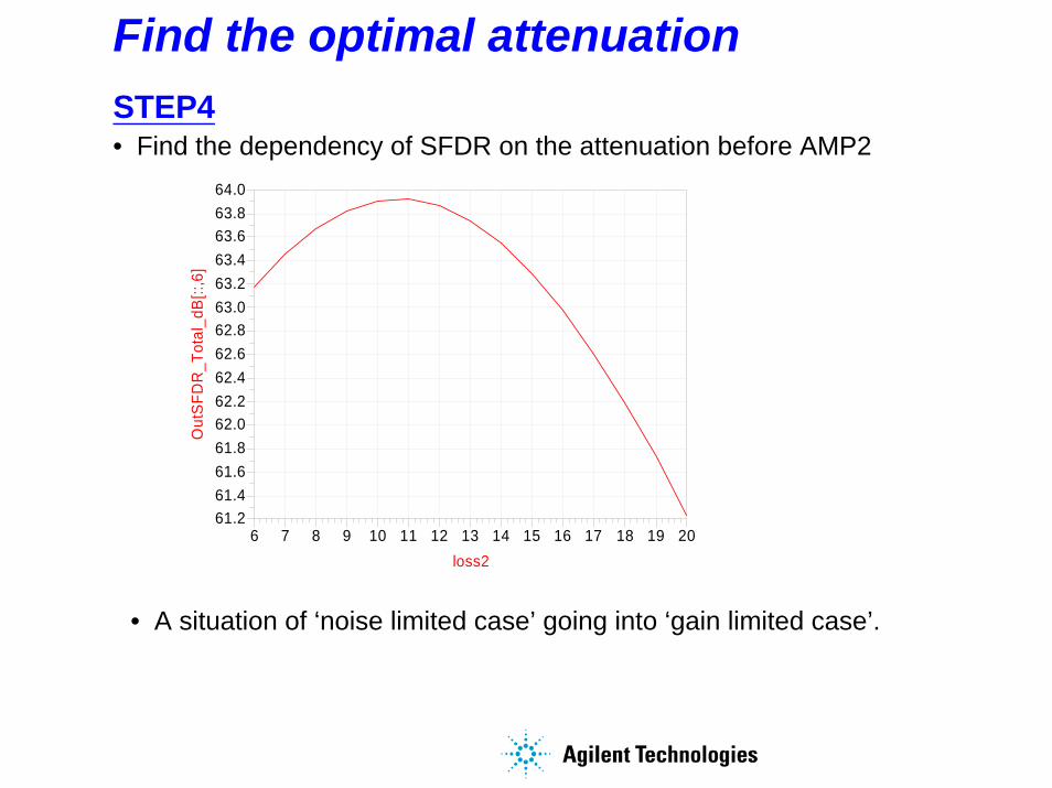
Find the optimal attenuationSTEP4• Find the dependency of SFDR on the attenuation before AMP2
7 8 9 10 11 12 13 14 15 16 17 18 196 20
61.461.661.862.062.262.462.662.863.063.263.463.663.8
61.2
64.0
loss2
Out
SFD
R_T
otal
_dB
[::,6
]
• A situation of ‘noise limited case’ going into ‘gain limited case’.
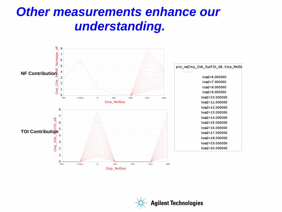
Other measurements enhance ourunderstanding.
ATTEN1 X1 MIX2 BPF3 PAD1BPF1 AMP2
1
2
3
4
5
6
7
0
8
Cmp_RefDes
Cm
p_C
trb_S
ysN
F_N
oIm
age_
dB
p lot_vs(Cmp_Ctrb_SysTOI_dB, Cmp_RefDe
loss2=6.000000loss2=7.000000loss2=8.000000loss2=9.000000
loss2=10.000000loss2=11.000000loss2=12.000000loss2=13.000000loss2=14.000000loss2=15.000000loss2=16.000000loss2=17.000000loss2=18.000000loss2=19.000000loss2=20.000000
ATTEN1 X1 MIX2 BPF3 PAD1BPF1 AMP2
1
2
3
4
5
6
7
0
8
Cmp_RefDes
Cm
p_C
trb_S
ysTO
I_dB
p lot_vs(Cmp_Ctrb_SysTOI_dB, Cmp_RefDe
loss2=6.000000loss2=7.000000loss2=8.000000loss2=9.000000
loss2=10.000000loss2=11.000000loss2=12.000000loss2=13.000000loss2=14.000000loss2=15.000000loss2=16.000000loss2=17.000000loss2=18.000000loss2=19.000000loss2=20.000000
NF Contribution
TOI Contribution
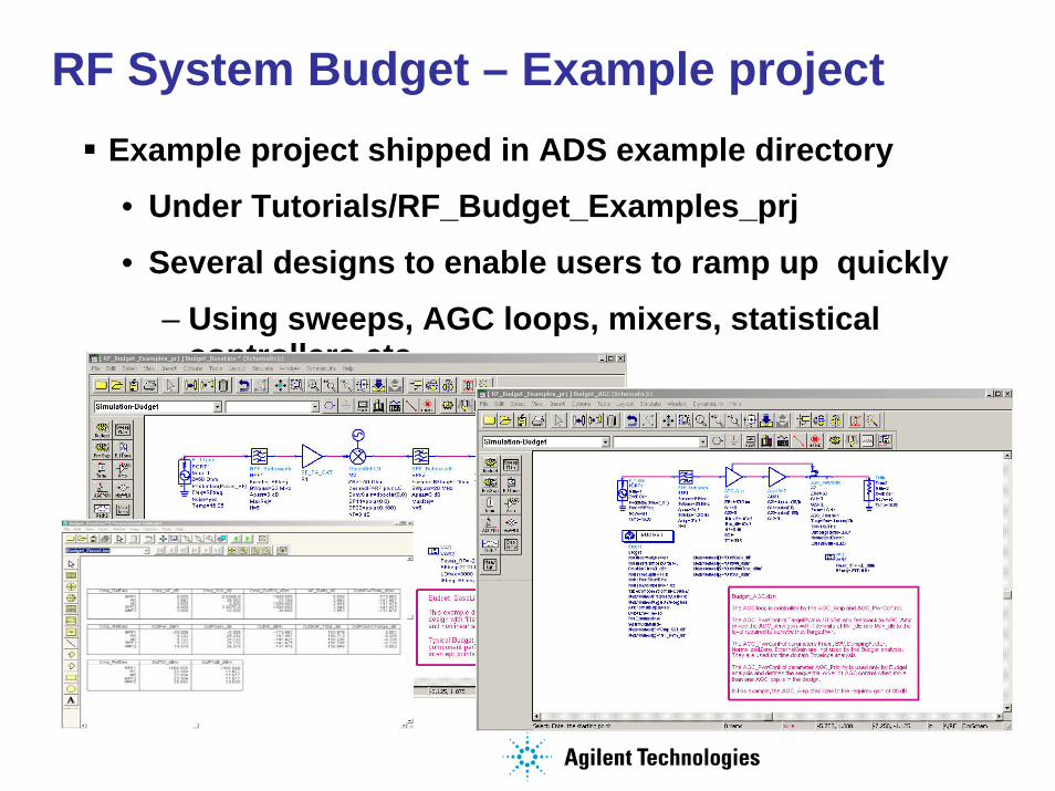
RF System Budget – Example projectExample project shipped in ADS example directory
• Under Tutorials/RF_Budget_Examples_prj
• Several designs to enable users to ramp up quickly
– Using sweeps, AGC loops, mixers, statistical controllers etc.
Budget Example Summary:
• The ADS budget controller is an effective way to quickly budget circuit level specifications
• ADS behavioral modeling and simulators are used
• Data can be formatted in a variety of ways to provide insight into RF System behaviors

广 告 页
Agilent ADS中文学习培训课程套装ADS中文学习培训课程套装是迄今为止国内最全面最权威的ADS培训教程,详细全面地讲解了ADS在微波射频电路、通信系统和电磁仿真设计方面的内容。套装中的中文视频培训课程是由具有多年
ADS使用经验的微波射频和通信领域资深专家讲解,工程实践强,且视频演示直观易学,能让您在最短的时间内学会使用ADS,并把ADS真正应用到微波射频电路和通信系统设计研发工作中去...。详情请浏览网址:http://www.mweda.com/eda/agilent.html
矢量网络分析仪学习套装
矢量网络分析仪是微波射频工程师研发调试工作中常用的测
试仪器之一,为了帮助微波射频工程师最迅速、全面地熟悉掌握矢
量网络分析仪使用,微波EDA网推出了这套矢量网络分析仪学习培训教程套装。套装中既有直观易学的矢量网络分析仪使用操作视频
教程,也有全面的矢网用户操作手册,详情请浏览网址: http://www.mweda.com/vna/course
台湾中华射频/通信专业视频课程套装
台湾中华大学教授给岛内知名电子企业员工培训课程视频,由
于是给企业员工培训,所以讲课内容尽量摒弃繁琐的数学推导、抽
象的概念,多从工程实践出发,以通俗易懂的语言和直观工程实例
来向学员讲述微波射频电路和数字通信系统相关知识。是从事微波
射频电路设计和通信系统设计相关工程技术人员不可多得的经典学
习教程。详情请浏览网址:http://www.mweda.com/vedio/vedio_45.html
Cadence Allegeo PCB设计培训套装
衡量一个软件的优劣,其中一个很现实的标准就是看它的市场
占有率,Cadence Allegro现在几乎成为高速板设计中实际上的工业标准,被很多大型电子通信类公司采用,因此掌握Cadence Allegro对找份好工作有实质的帮助;另外其学习资源也比较丰富,比较适
合自学。本站现推出Cadence Allegro PCB设计培训套装,实用易学,物超所值,帮助您迅速有效的学习掌握Allegeo PCB设计。详情请浏览网址:http://www.mweda.com/eda/allegro.html
>> 更多微波射频和PCB设计相关培训课程尽在 微波EDA网
Related Documents