DESIGN OF ULTRA-WIDEBAND (2-18 GHz) BUTLER MATRIX A Thesis by INDERDEEP SINGH Submitted to the Office of Graduate and Professional Studies of Texas A&M University in partial fulfillment of the requirements for the degree of MASTER OF SCIENCE Chair of Committee, Gregory H. Huff Co-Chair of Committee, Robert D. Nevels Committee Members, Jean-Francois Chamberland Darren Hartl Head of Department, Miroslav M. Begovic December 2019 Major Subject: Electrical Engineering Copyright 2019 Inderdeep Singh

Welcome message from author
This document is posted to help you gain knowledge. Please leave a comment to let me know what you think about it! Share it to your friends and learn new things together.
Transcript
DESIGN OF ULTRA-WIDEBAND (2-18 GHz) BUTLER MATRIX
A Thesis
by
INDERDEEP SINGH
Submitted to the Office of Graduate and Professional Studies of
Texas A&M University
in partial fulfillment of the requirements for the degree of
MASTER OF SCIENCE
Chair of Committee, Gregory H. Huff
Co-Chair of Committee, Robert D. Nevels
Committee Members, Jean-Francois Chamberland
Darren Hartl
Head of Department, Miroslav M. Begovic
December 2019
Major Subject: Electrical Engineering
Copyright 2019 Inderdeep Singh

ii
ABSTRACT
This thesis presents the design of an ultra-wide band hybrid coupler, crossover
and phase shifters for the design of four-input, four-output (4x4) stripline Butler matrix
in order to feed an antenna array in 2-18 GHz frequency range. The goal of this thesis is
to develop an antenna-array feeding passive microwave network based on Butler matrix
with a ultra-wide bandwidth which works as ground work for realization of eight input,
eight output Butler matrix. Further the 4x4 and 8x8 Butler matrix can be used in a row-
card configuration to realize 16x16 and 64x64 Butler matrix. In order to meet the ultra-
wide band requirements, wide band passive microwave components such as hybrid
coupler, crossovers and phase-shifters are designed, which operate from 2 to 18 GHz.
The Butler matrix can be used as a beam-forming network produces orthogonal beams
which can be steered in different directions.

iii
ACKNOWLEDGEMENTS
I would like to thank my committee chair, Dr. Gregory Huff, my co-chair Dr.
Robert Nevels and my committee members, Dr. Jean-Francois Chamberland and Dr.
Darren Hartl for their guidance and support throughout the course of this research.
Thanks also go to my friends and colleagues and the department faculty and staff
for making my time at Texas A&M University a great experience.
Finally, thanks to family for their constant encouragement.

iv
CONTRIBUTORS AND FUNDING SOURCES
This work was supervised by a thesis committee consisting of Professors
Gregory H. Huff (advisor) ,Robert D. Nevels and Jean-Francois Chamberland of the
Department of Electrical and Computer Engineering and Professor Darren Hartl of the
Department of Aerospace Engineering.
All work for the thesis was completed independently by the student.
There are no outside funding contributions to acknowledge related to the research
and compilation of this document.

v
TABLE OF CONTENTS
Page
ABSTRACT .................................................................................................................. ii
ACKNOWLEDGEMENTS ......................................................................................... iii
CONTRIBUTORS AND FUNDING SOURCES ........................................................ iv
TABLE OF CONTENTS .............................................................................................. v
LIST OF FIGURES ..................................................................................................... vii
1. INTRODUCTION ..................................................................................................... 1
1.1. Butler Matrix ...................................................................................................... 2 1.2. 90° Hybrid Coupler ............................................................................................ 5 1.3. Crossover ............................................................................................................ 6 1.4. Phase Shifters ..................................................................................................... 8
2. HYBRID COUPLER ................................................................................................ 9
2.1. Coupling Structures ............................................................................................ 9 2.2. Even and Odd Mode Impedances..................................................................... 11 2.3. Braodband Couplers ......................................................................................... 14 2.4. Coupler Design ................................................................................................. 22
3. CROSSOVER DESIGN .......................................................................................... 31
4. PHASE SHIFTER DESIGN ................................................................................... 34
5. 4X4 BUTLER MATRIX DESIGN AND RESULTS ............................................. 44
6. FUTURE WORK .................................................................................................... 50
6.1. TRL Calibration Kit ......................................................................................... 50 6.2. 8X8 Butler Matrix ............................................................................................ 53 6.3. 16X16 Butler Matrix ........................................................................................ 54 6.4. 64X64 Butler Matrix ........................................................................................ 58
7. CONCLUSIONS ..................................................................................................... 59

vi
REFERENCES ............................................................................................................ 60

vii
LIST OF FIGURES
Page
Figure 1-1 : 2x2 Butler Matrix Schematic .................................................................... 3
Figure 1-2 : 4x4 Butler matrix schematic ...................................................................... 4
Figure 1-3 : 8x8 Butler matrix schematic ...................................................................... 4
Figure 1-4 : Hybrid Coupler .......................................................................................... 5
Figure 1-5 : Crossover as Tandem Connection of Hybrid Couplers ............................. 6
Figure 2-1 : Coupled transmission lines (a) edge coupled microstrip, (b) edge
coupled striplines, (c) broadside coupled striplines, (d) offset coupled
striplines ....................................................................................................... 10
Figure 2-2 : Representation of capacitances on coupled lines .................................... 12
Figure 2-3 : Even mode excitation of coupled lines .................................................... 12
Figure 2-4 : Odd mode excitation in coupled lined ..................................................... 13
Figure 2-5 : Slot Coupled Microstrip Coupler ............................................................ 16
Figure 2-6 : Magnitude response of single section slot coupled microstrip coupler ... 16
Figure 2-7 : 3-Section slot coupled microstrip coupler ............................................... 17
Figure 2-8 : Magnitude and phase response of 3-section slot coupled microstrip
coupler (a) Magnitude Response (b) Phase Response ................................. 18
Figure 2-9 : 5-Section slot coupled microstrip coupler ............................................... 19
Figure 2-10 : Magnitude Response of 5-section slot coupled microstrip coupler....... 19
Figure 2-11 : 3 dB coupler as a tandem connection of two 8.34 dB couplers ............ 21
Figure 2-12 : 7-section 8.34 dB stripline coupler (a) Top view (b) Trimetric view ... 26
Figure 2-13 : Geometry of stripline structures ............................................................ 26
Figure 2-14 : Magnitude and phase response of 7-section 8.34 dB coupler (a)
Magnitude response (b) Phase response ...................................................... 27
viii
Figure 2-15 : 3 dB coupler as a tandem connection of two 8.34 dB couplers (a) Top
view (b) Trimetric view ............................................................................... 28
Figure 2-16 : Magnitude and phase response of 3 dB coupler .................................... 29
Figure 3-1 : Crossover design as a tandem connection of two 3 dB couplers (a) Top
View (b) Trimetric View ............................................................................. 32
Figure 3-2 : Crossover magnitude response ................................................................ 33
Figure 4-1 : Schiffman phase shifter ........................................................................... 34
Figure 4-2 : Phase response of single section 90° Schiffman phase shifters .............. 36
Figure 4-3 : 5-section Schiffman phase shifter with a straight reference line ............. 38
Figure 4-4 : Schiffman phase shifter with reference line showing the de-embed ....... 38
Figure 4-5 : Phase response of 5-section 45 degrees Schiffman phase shifter with
respect to a straight line ............................................................................... 39
Figure 4-6 : Phase shifter with extra lengths to compensate for crossover phase
response ....................................................................................................... 40
Figure 4-7 : Phase response of 5-section 45 degrees Schiffman phase shifter with
respect to crossover ...................................................................................... 41
Figure 4-8 : Phase response of 6-section 45 degrees Schiffman phase shifter with
respect to crossover ...................................................................................... 41
Figure 4-9 : Phase response of 6-section 67.5 degrees Schiffman phase shifter with
respect to crossover ...................................................................................... 42
Figure 4-10 : Phase response of 6-section degrees Schiffman phase shifter with
respect to crossover ...................................................................................... 43
Figure 5-1 : Layout of 4x4 ultra-wideband Butler matrix (Top View) ....................... 45
Figure 5-2 : Layout of ultra-wideband Butler matrix (Trimetric view) ...................... 46
Figure 5-3 : Magnitude Response of Butler matrix with respect to Port 1 ................. 47
Figure 5-4 : Magnitude response of Butler matrix with respect to Port 2 ................... 47
Figure 5-5 : Butler Matrix progressive phase shifts of 45° with respect to Port 1 ...... 48
ix
Figure 5-6 : Butler Matrix progressive phase shifts of 135° with respect to Port 2 .... 49
Figure 6-1 : Through standard ..................................................................................... 50
Figure 6-2 : Reflect standard ....................................................................................... 51
Figure 6-3 : Line standards .......................................................................................... 51
Figure 6-4 : Two-port response of hybrid coupler without calibration kit .................. 52
Figure 6-5 : Two-port response of hybrid coupler with calibration kit ....................... 53
Figure 6-6 : Schematic view of row card configuration of 16x16 Butler matrix from
4x4 Butler matrix ......................................................................................... 55
Figure 6-7 : Designed 4x4 Butler matrix stacked in row-card configuration to form
16x16 Butler matrix ..................................................................................... 55
Figure 6-8 : Circuit schematic of 16x16 Butler matrix from 4x4 Butler matrices ...... 56
Figure 6-9 : Ideal magnitude response of 16x16 Butler matrix designed as row card
configuration of 4x4 Butler matrix .............................................................. 57
Figure 6-10 : Ideal phase response of 16x16 Butler matrix designed as row card
configuration of 4x4 Butler matrix .............................................................. 57
Figure 6-11 : Schematic view of row card configuration of 64x64 Butler matrix from
8x8 Butler matrix ......................................................................................... 58
1
1. INTRODUCTION
Beam-forming or spatial filtering techniques have an extensive range of
applications including but not limited to defense [1, 2], automotive communications [3]
and cellular communications [4]. The upcoming 5G technology for cellular
communication has strong dependence on beam-forming to form a direct link between
the receiver and sender to counter the attenuation of millimeter waves [5]. A beam-
forming network generates the required amplitude and phase excitations, to steer the
radiated beam to a specific spatial direction without changing the physical locations of
the antenna elements. Examples include, the digital beam-forming networks [6], the
circuit based beam-forming networks such as Butler Matrix [7] and Blass Matrix [8] and
the Microwave lens beam-forming networks such as Rotman lens [9] and Luneberg lens
[10] .
While digital beam-forming networks provide better performance with very low
phase errors and more flexible amplitude tapering, they are not suitable for high
frequencies and requires large hardware and enormous power as the aperture size or the
number of antenna elements increase. Butler matrix network is easy to construct and
implement on printed circuit boards. By varying the input current amplitude and input
phase to the Butler matrix the beam can be scanned to the required direction. Sheleg
discusses the design and implementation of Butler matrix based scanning using circular
array [11]. Tayeb et al. described a 4x4 Butler matrix design for linear microstrip
antenna array operating at 1.9 GHz [12]. Mourad et al. have designed 4x4 Butler matrix
2
using coplanar waveguides at 5.8 GHz [13]. In this work ultra-wideband (2-18 GHz)
stripline Butler matrix design is proposed. Individual building blocks, hybrid coupler,
crossover, phase shifter are first designed for 2-18 GHz. Further they are put together to
form 4x4 Butler matrix.
1.1. Butler Matrix
A butler matrix is a passive microwave beamforming network used to feed a
phased antenna array. It was first proposed by Butler and Lowe in 1961 [14]. To steer
the beam using a phased antenna array, current phase needs to be varied. Each antenna
element in the phased array can be fed with progressive phase shifts to steer the beam in
a specific direction. Butler matrix facilitates this operation by feeding current to the
antenna elements in a progressive phase shift manner.
A Butler matrix is an N-input N-output passive microwave network, where N is
generally some power of 2. Power is applied at the N-input ports and the progressive
phase shifts are obtained at the N-output ports to which N antenna elements are
connected. The N-input ports are also called the beam ports and the N-output ports are
called the antenna ports. The beam direction can be controlled by which input or beam
port is excited. The input at any one beam port results in current of equal amplitude and
linearly varying phase at the antenna ports. This kind of operation is generally called
switched beam, where the input is switched to one of the beam ports. Multiple beam
ports can also be simultaneously fed. For example, if two ports are fed simultaneously,
the antenna array radiates dual beams simultaneously, superimposed on one another.
3
The phase difference between the antenna ports varies depending on which beam
port is excited. In general for an N-input port Butler matrix if Kth (K = ± 1, ± 2, ± 3..
±N/2) port is excited the phase difference between output ports is ± (2K-1)/N. For the
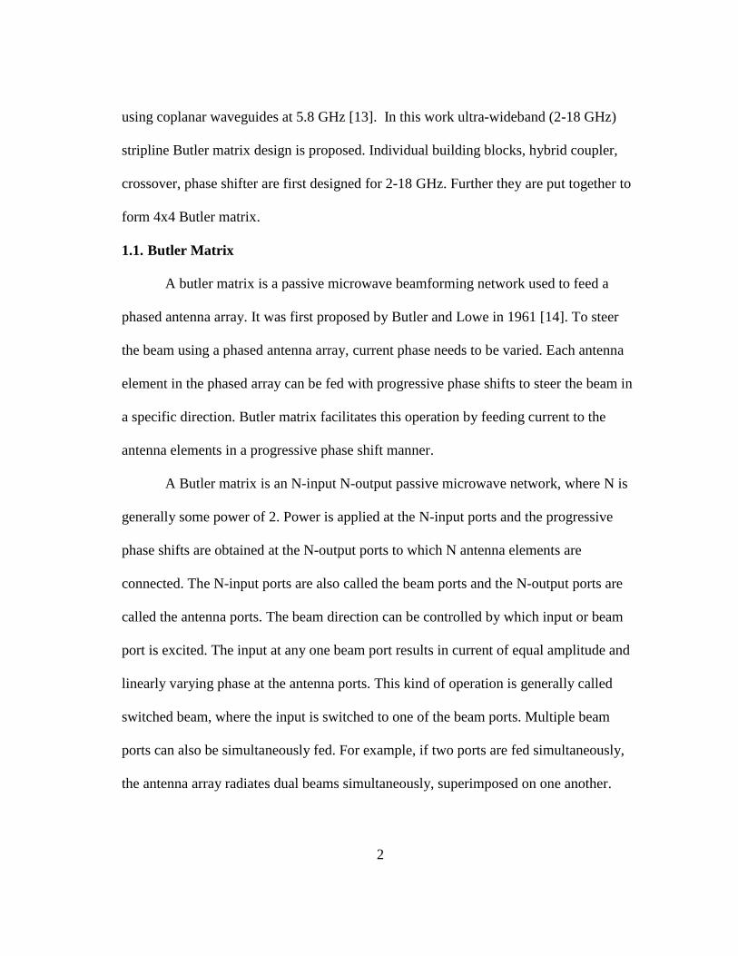
simple case of 2x2 Butler matrix the phase difference between output ports is ±90°.
Therefore a 2x2 Butler matrix is simply a 90° hybrid coupler. Figure 1-1 shows a block
diagram of such a Butler matrix. In general N-port Butler matrix is a passive network
formed by a combination of 90° hybrid couplers, crossovers and phase shifters.
Figure 1-1 : 2x2 Butler Matrix Schematic
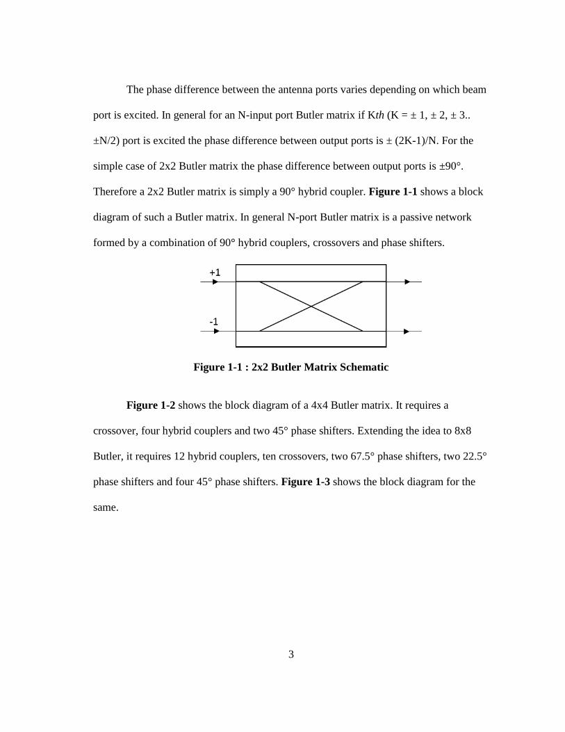
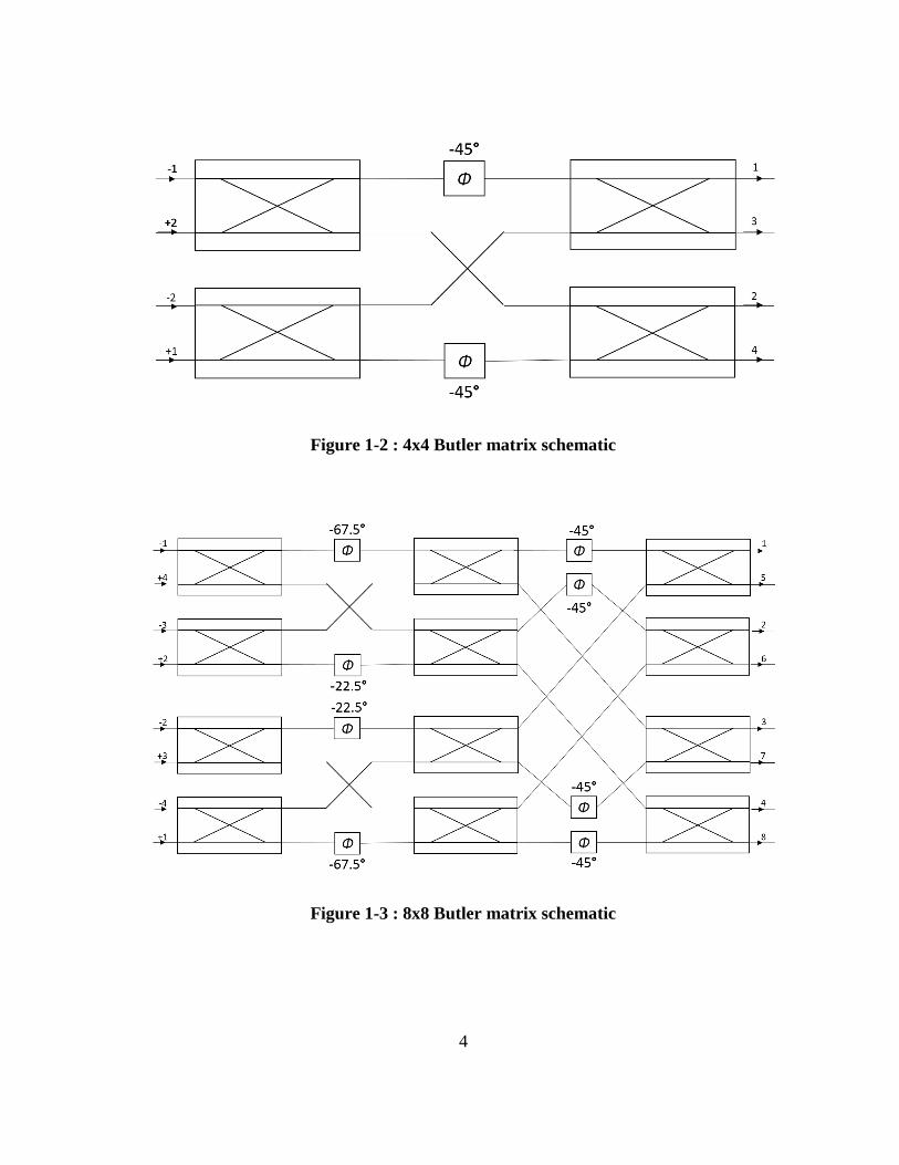
Figure 1-2 shows the block diagram of a 4x4 Butler matrix. It requires a
crossover, four hybrid couplers and two 45° phase shifters. Extending the idea to 8x8
Butler, it requires 12 hybrid couplers, ten crossovers, two 67.5° phase shifters, two 22.5°
phase shifters and four 45° phase shifters. Figure 1-3 shows the block diagram for the
same.
4
Figure 1-2 : 4x4 Butler matrix schematic
Figure 1-3 : 8x8 Butler matrix schematic
5
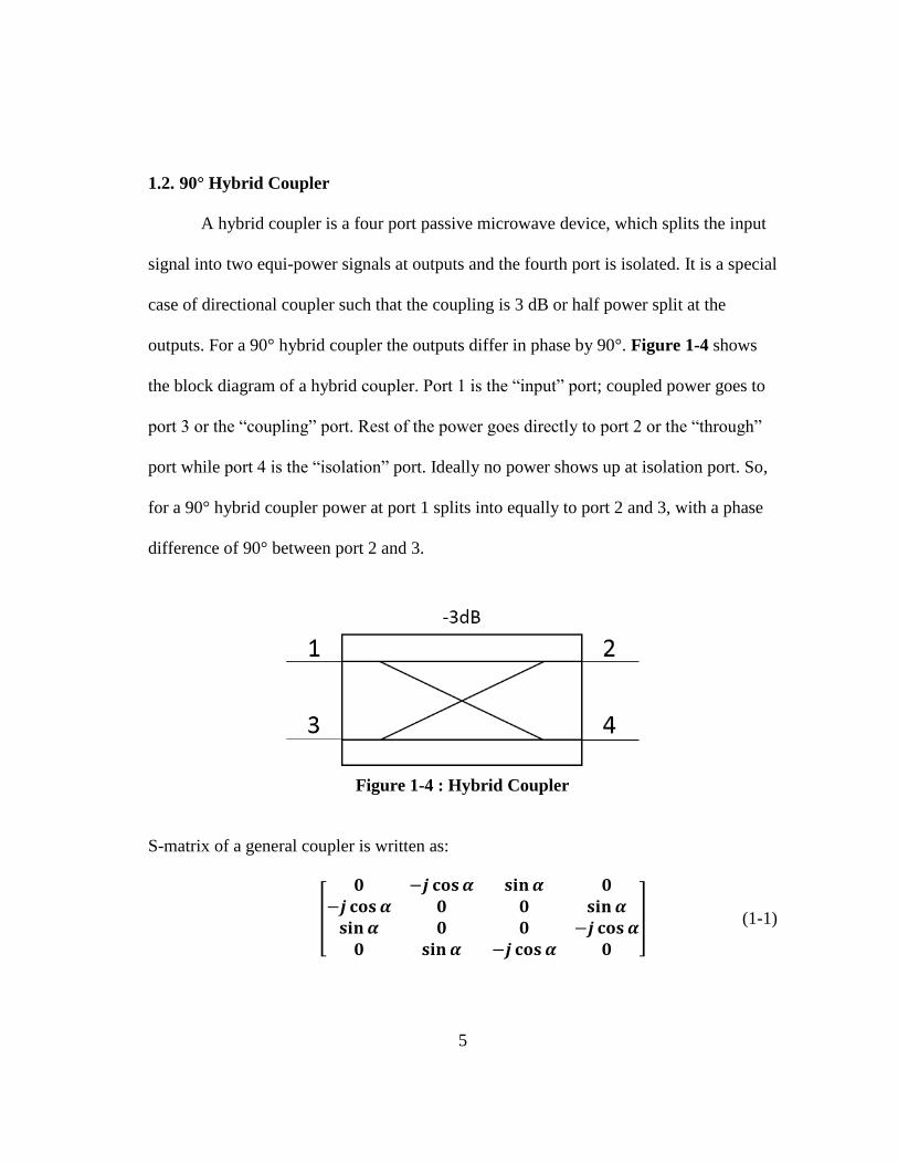
1.2. 90° Hybrid Coupler
A hybrid coupler is a four port passive microwave device, which splits the input
signal into two equi-power signals at outputs and the fourth port is isolated. It is a special
case of directional coupler such that the coupling is 3 dB or half power split at the
outputs. For a 90° hybrid coupler the outputs differ in phase by 90°. Figure 1-4 shows
the block diagram of a hybrid coupler. Port 1 is the “input” port; coupled power goes to
port 3 or the “coupling” port. Rest of the power goes directly to port 2 or the “through”
port while port 4 is the “isolation” port. Ideally no power shows up at isolation port. So,
for a 90° hybrid coupler power at port 1 splits into equally to port 2 and 3, with a phase
difference of 90° between port 2 and 3.
S-matrix of a general coupler is written as:
[
𝟎 −𝒋 𝐜𝐨𝐬𝜶 𝐬𝐢𝐧𝜶 𝟎−𝒋 𝐜𝐨𝐬 𝜶 𝟎 𝟎 𝐬𝐢𝐧𝜶
𝐬𝐢𝐧𝜶 𝟎 𝟎 −𝒋 𝐜𝐨𝐬 𝜶𝟎 𝐬𝐢𝐧𝜶 −𝒋 𝐜𝐨𝐬 𝜶 𝟎
] (1-1)
Figure 1-4 : Hybrid Coupler
6
where sin α = k is the voltage coupling coefficient. For the hybrid coupler, since coupled
power is ½ therefore the voltage coupling coefficient, k becomes √ ½ or α = π/4.
Based on the application, the frequency of operation, 90° hybrid coupler can be
realized as coupled line coupler, branchline coupler, Lange coupler or interdigitated
coupler etc. in transmission line structures such as microstrip, stripline, waveguide etc.
Section 2 covers the design choices available for this particular application where 3 dB
coupling is required over 2-18 Ghz and the finalized stripline design with its simulated
results in HFSS.
1.3. Crossover
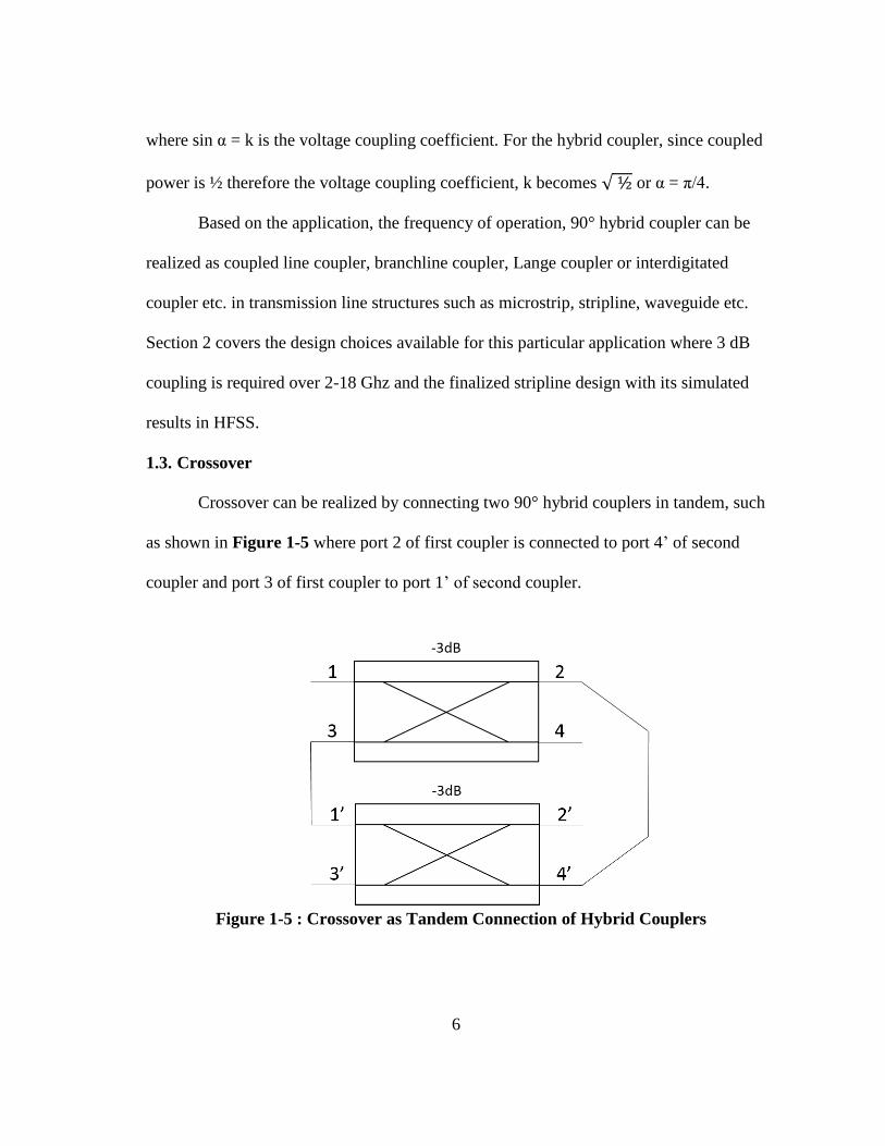
Crossover can be realized by connecting two 90° hybrid couplers in tandem, such
as shown in Figure 1-5 where port 2 of first coupler is connected to port 4’ of second
coupler and port 3 of first coupler to port 1’ of second coupler.
Figure 1-5 : Crossover as Tandem Connection of Hybrid Couplers

7
When input port of the first coupler is excited by a unity wave voltage, the
voltage waves amplitude and phase at the other ports can be obtained using the S-matrix
of the 90° hybrid. Using voltage coupling coefficient of k = √ ½,
[
𝑽𝟏−
𝑽𝟐−
𝑽𝟑−
𝑽𝟒−
] =
[
𝟎 −𝒋√ ½ √ ½ 𝟎
−𝒋√ ½ 𝟎 𝟎 √ ½
√ ½ 𝟎 𝟎 −𝒋√ ½
𝟎 √ ½ −𝒋√ ½ 𝟎 ]
[
𝟏𝟎𝟎𝟎
] (1-2)
which gives,
𝑽𝟏− = 𝟎 (1-3)
𝑽𝟐− = −𝒋√ ½ (1-4)
𝑽𝟑− = √ ½ (1-5)
𝑽𝟒− = 𝟎 (1-6)
Now, 𝑽𝟐− and 𝑽𝟑
− are the incident voltage waves at port 1 and port 4 of the second
coupler, therefore the reflected voltages of coupler 2 can be obtained as:
[
𝑽𝟏′−
𝑽′𝟐−
𝑽′𝟑−
𝑽′𝟒−]
=
[
𝟎 −𝒋√ ½ √ ½ 𝟎
−𝒋√ ½ 𝟎 𝟎 √ ½
√ ½ 𝟎 𝟎 −𝒋√ ½
𝟎 √ ½ −𝒋√ ½ 𝟎 ]
[
𝟎−𝒋√ ½
√ ½𝟎
] (1-7)
which leads to,
𝑽′𝟏− = 𝟎 (1-8)
𝑽′𝟐− = −𝒋 (1-9)
𝑽′𝟑− = 0 (1-10)
𝑽′𝟒− = 𝟎 (1-11)

8
According to the analysis above, when two hybrids are connected in tandem all of the
input power comes out through port 2 of the second coupler.
Hence design of crossover for the realization of Butler matrix is straightforward
once design topology of 90° hybrid coupler is fixed.
1.4. Phase Shifters
Phase shifters are critical components in numerous RF systems including linear
power amplifiers (Doherty amplifier) and phased array systems as in this application.
For Butler Matrix the phase shift required as shown in Figure 1-2 and Figure 1-3 are
with respect to the crossovers and any extra line lengths that can be attributed to the
layout of Butler Matrix. For broadband designs, challenge lies in designing phase
shifters that can provide a flat phase shift throughout the bandwidth of interest, ie. 2-18
GHz.
Ideally, the power at the output of phase shifter should be equal to the input
power, which implies an insertion loss of 0 dB. But due to the finite non-ideal
transmission line length, there are dielectric and conductor losses which degrade the
insertion loss. These losses are more significant at higher frequencies.
9
2. HYBRID COUPLER
As described on last section, hybrid coupler is one of the key building blocks for
the design of Butler matrix. For this design, the frequency of operation is 2-18 Ghz,
hence the an ultra-wideband 90° hybrid coupler is required with 3dB coupling and 90°
phase difference between the through and coupled ports over the entire frequency range.
The challenge of the design inherently lies in the ultra-wideband operation. Such wide
bandwidth of operation is practically not possible with a single section coupler.
2.1. Coupling Structures
When two or more transmission lines are present in close proximity to each
other, due to the interaction of electric and magnetic fields, power from one line is
coupled to another. Specifically, in a two transmission line system, if the primary
transmission line is excited, power couples to the secondary transmission line. The
coupled power is a function of the dimensions of the transmission lines, dielectric media,
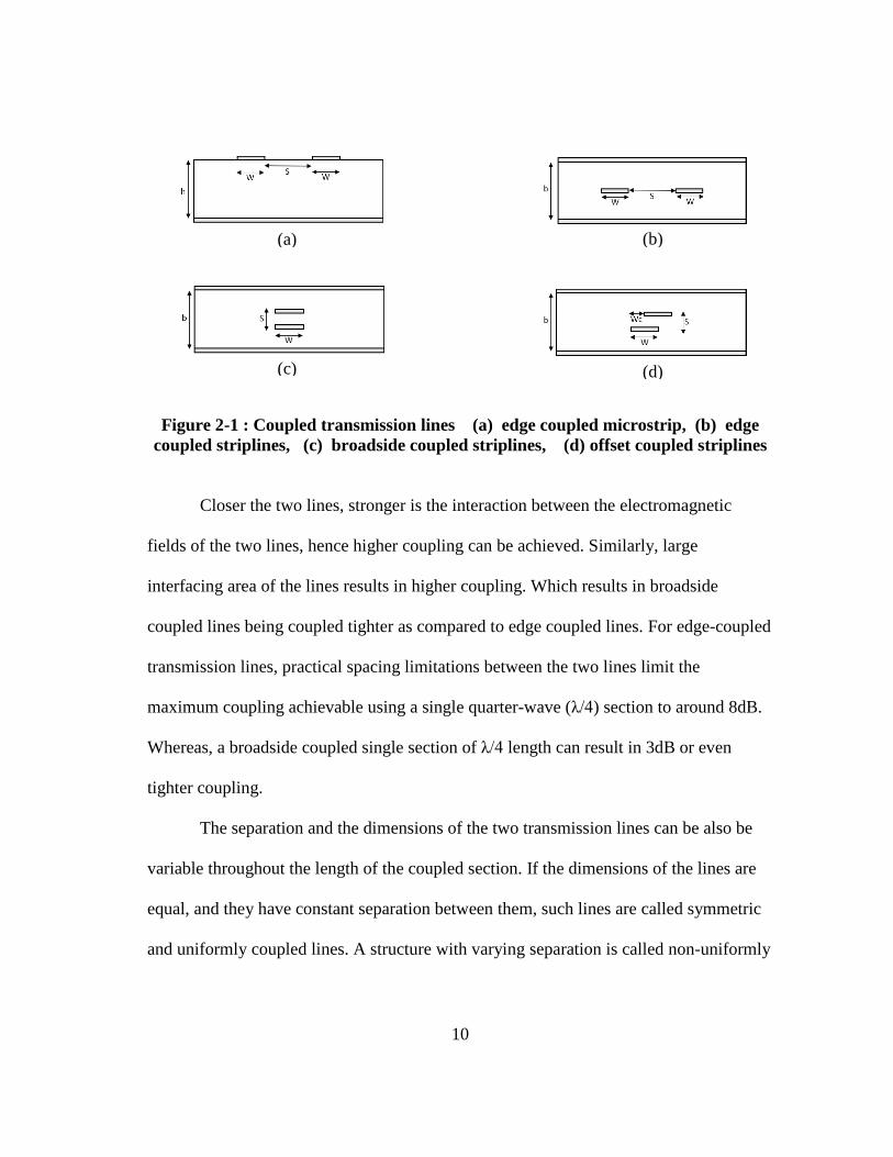
mode of propagation and frequency of operation. Such coupling structures could either
be edge coupled, broadside coupled or offset coupled as shown in Figure 2-1. Since
microstrip lines lie in the same plane they can only be design as edge coupled.
10
Figure 2-1 : Coupled transmission lines (a) edge coupled microstrip, (b) edge
coupled striplines, (c) broadside coupled striplines, (d) offset coupled striplines
Closer the two lines, stronger is the interaction between the electromagnetic
fields of the two lines, hence higher coupling can be achieved. Similarly, large
interfacing area of the lines results in higher coupling. Which results in broadside
coupled lines being coupled tighter as compared to edge coupled lines. For edge-coupled
transmission lines, practical spacing limitations between the two lines limit the
maximum coupling achievable using a single quarter-wave (λ/4) section to around 8dB.
Whereas, a broadside coupled single section of λ/4 length can result in 3dB or even
tighter coupling.
The separation and the dimensions of the two transmission lines can be also be
variable throughout the length of the coupled section. If the dimensions of the lines are
equal, and they have constant separation between them, such lines are called symmetric
and uniformly coupled lines. A structure with varying separation is called non-uniformly
(a) (b)
(c) (d)
11
coupled lines and structure with varying widths of lines is called asymmetric coupled
lines.
The coupling between the two coupled transmission lines is described in terms of
even and odd modes of excitation. In even-mode excitation the two transmission lines
are at equal potentials and in odd-mode the lines are at equal but opposite polarity
potential. The coupling is defined in terms of characteristic impedances of these two
modes. When both lines are excited in phase with equal amplitude (even-mode), the
impedance from one line to the ground is the even-mode characteristic impedance (𝒁𝟎𝒆).
Similarly, when the lines are excited in opposite phase but equal amplitude (odd-mode),
the impedance from one line to ground is the odd-mode characteristic impedance (𝒁𝟎𝒐).
Voltage coupling coefficients of the coupled line structures are expressed in terms of
these even and odd-mode characteristic impedances, length of the coupled structures and
the effective dielectric constant. For homogenous transmission lines of λ/4 length, the
voltage coupling coefficient, k is
𝒌 = 𝒁𝟎𝒆 − 𝒁𝟎𝒐
𝒁𝟎𝒆 + 𝒁𝟎𝒐 (2-1)
2.2. Even and Odd Mode Impedances
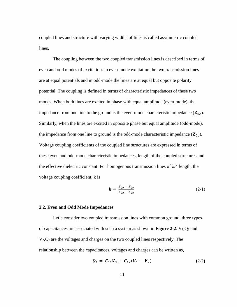
Let’s consider two coupled transmission lines with common ground, three types
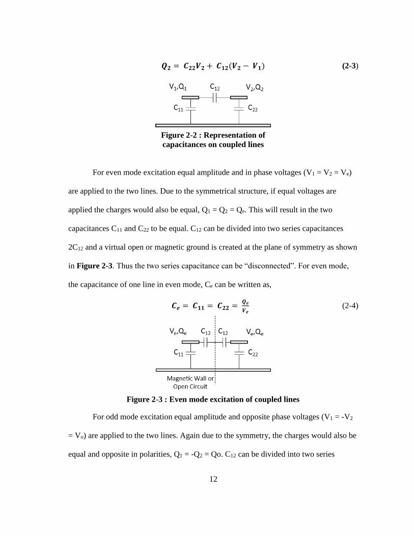
of capacitances are associated with such a system as shown in Figure 2-2. V1,Q1 and
V2,Q2 are the voltages and charges on the two coupled lines respectively. The
relationship between the capacitances, voltages and charges can be written as,
𝑸𝟏 = 𝑪𝟏𝟏𝑽𝟏 + 𝑪𝟏𝟐(𝑽𝟏 − 𝑽𝟐) (2-2)
12
𝑸𝟐 = 𝑪𝟐𝟐𝑽𝟐 + 𝑪𝟏𝟐(𝑽𝟐 − 𝑽𝟏) (2-3)
For even mode excitation equal amplitude and in phase voltages (V1 = V2 = Ve)
are applied to the two lines. Due to the symmetrical structure, if equal voltages are
applied the charges would also be equal, Q1 = Q2 = Qe. This will result in the two
capacitances C11 and C22 to be equal. C12 can be divided into two series capacitances
2C12 and a virtual open or magnetic ground is created at the plane of symmetry as shown
in Figure 2-3. Thus the two series capacitance can be “disconnected”. For even mode,
the capacitance of one line in even mode, Ce can be written as,
𝑪𝒆 = 𝑪𝟏𝟏 = 𝑪𝟐𝟐 = 𝑸𝒆
𝑽𝒆(2-4)
For odd mode excitation equal amplitude and opposite phase voltages (V1 = -V2
= Vo) are applied to the two lines. Again due to the symmetry, the charges would also be
equal and opposite in polarities, Q1 = -Q2 = Qo. C12 can be divided into two series
Figure 2-2 : Representation of
capacitances on coupled lines
Figure 2-3 : Even mode excitation of coupled lines
13
capacitances 2C12 and a virtual ground or electric ground is created the plane of
symmetry as shown in Figure 2-4. Thus,
𝑸𝒐 = (𝑪𝟏𝟏 + 𝟐𝑪𝟏𝟐)𝑽𝒐 (2-5)
or
𝑪𝒐 = (𝑪𝟏𝟏 + 𝟐𝑪𝟏𝟐) = 𝑸𝒐
𝑽𝒐 (2-6)
where Co is the capacitance of one line for odd mode excitation.
The magnetic wall and electric wall plane of symmetry for even and odd modes
respectively make the analysis of calculating capacitances Ce and Co easier by just
considering half the structure.
Characteristic impedance of transmission line is related to capacitance per unit
length,
𝒁𝟎 = 𝟏
𝒗𝒑 𝑪(2-7)
Where vp is the phase velocity,
𝒗𝒑 = 𝒄
√𝜺𝒓(2-8)
Therefore even and odd mode characteristic impedances are,
𝒁𝟎𝒆 = 𝟏
𝒗𝒑𝒆 𝑪𝒆(2-9)
and
Figure 2-4 : Odd mode excitation in coupled lined
14
𝒁𝟎𝒐 = 𝟏
𝒗𝒑𝒐 𝑪𝒐 (2-10)
For homogeneous transmission lines such as striplines, the phase velocities of even and
odd modes are equal,
𝒗𝒑𝒆 = 𝒗𝒑𝒐 = 𝒄
√𝜺𝒓 (2-11)
For inhomogeneous transmission lines, for instance microstrip transmission lines, the
even and odd mode phase velocities are generally unequal,
𝒗𝒑𝒆 = 𝒄
√𝜺𝒓𝒆(2-12)
and
𝒗𝒑𝒐 = 𝒄
√𝜺𝒓𝒐(2-13)
Where 𝜺𝒓𝒆 and 𝜺𝒓𝒐 are effective even and odd mode dielectric constants.
2.3. Braodband Couplers
Multiple sections of quarter wave coupled lines can be cascaded, in order to
achieve near constant coupling over a wide bandwidth. It involves appropriate selection
of even and odd-mode impedances of each section. The relation between even- and odd-
mode impedance of each section is related by,
𝒁𝟎𝟐 = 𝒁𝟎𝒆 𝒁𝟎𝒐 (2-14)
where Z0 is the impedance of terminating ports of the coupler.
A symmetrical broadband coupler has odd number of sections. In such a coupler
the ith section is identical to the N+1-ith section and thus is symmetric around the
middle section. An asymmetric coupler lacks such symmetry and can employ even or
odd number of sections. In the case of symmetrical couplers the through and coupled
ports are 90° apart in phase, a property required for the design of Butler matrix.
15
In [15] Cristal and Young tabulated even and odd mode impedances, of each
section of multi-section coupler for number of sections, coupling coefficients and
fractional bandwidth for symmetrical TEM mode coupled lines. One way to realize the
required 90° hybrid coupler could be in microstrip multi-section edge coupled lines. But
the amount of coupling required for the middle sections is too high to be physically
realizable. For a practical realization of edge coupled microstrip lines, it is very hard to
achieve less than 8 dB of coupling since it requires too small spacing between the lines.
Moreover, transmission mode in microstrip lines is not purely TEM due to
inhomogeneous dielectric (air and the dielectric medium).The phase velocities of odd
and even mode are not equal, which leads to phase errors between the through and
coupled ports. [16] Employed wiggly lines in order to get equal phase velocities for
even- and odd- mode. Due to restriction in achievable coupling requirement of the
tightly coupled middle section, edge coupled micro-strip lines are not suitable for this
work.
For tighter coupling [17] proposed Lange or interdigitated couplers by increasing
the mutual capacitance between the lines. Interdigitated couplers are sensitive to small
gaps between the conductors. Also, it requires bond wires which can cause
manufacturing issues.
More recently [18] used slot coupled microstrip lines to achieve tighter coupling
over 3.1 to 10.6 GHz. It was followed by [19] where three sections were used to achieve
even higher bandwidth from 2.3 to 12.3 GHz. Using this design paradigm, a broadband
coupler was designed for our application for 2-18 GHz operation. Figure 2-5
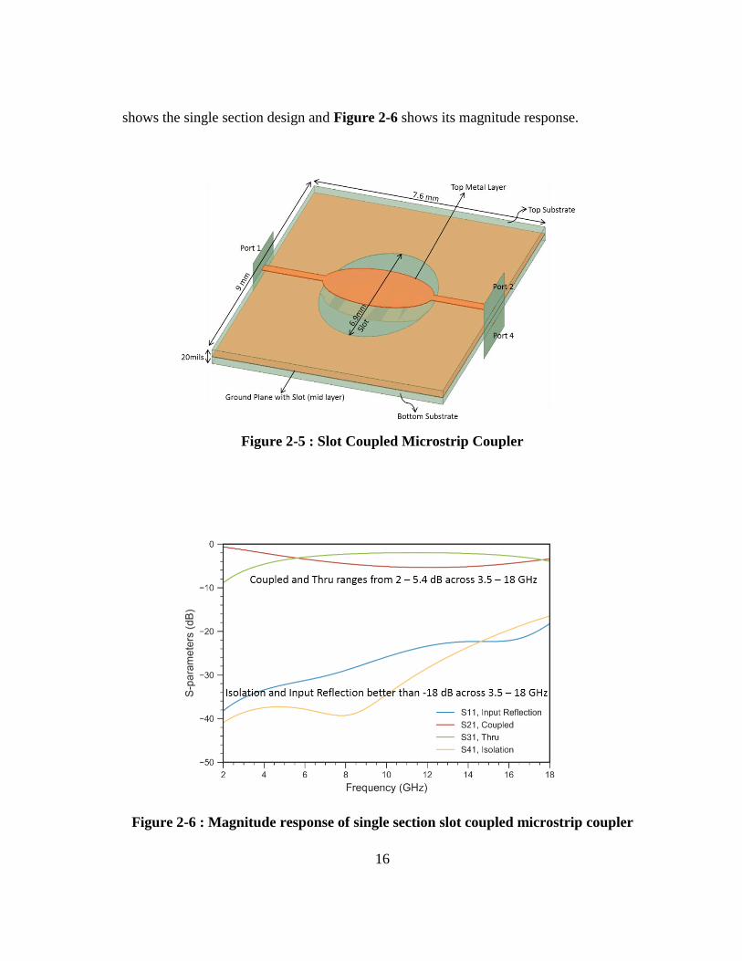
16
shows the single section design and Figure 2-6 shows its magnitude response.
Figure 2-6 : Magnitude response of single section slot coupled microstrip coupler
Figure 2-5 : Slot Coupled Microstrip Coupler
17
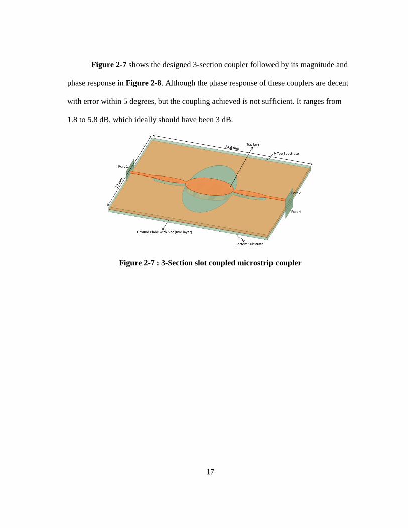
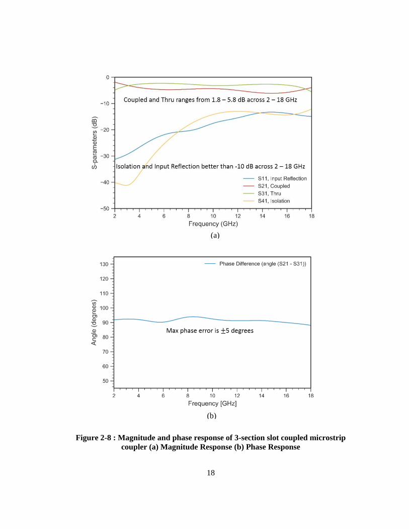
Figure 2-7 shows the designed 3-section coupler followed by its magnitude and
phase response in Figure 2-8. Although the phase response of these couplers are decent
with error within 5 degrees, but the coupling achieved is not sufficient. It ranges from
1.8 to 5.8 dB, which ideally should have been 3 dB.
Figure 2-7 : 3-Section slot coupled microstrip coupler
18
Figure 2-8 : Magnitude and phase response of 3-section slot coupled microstrip
coupler (a) Magnitude Response (b) Phase Response
(a)
(b)
19
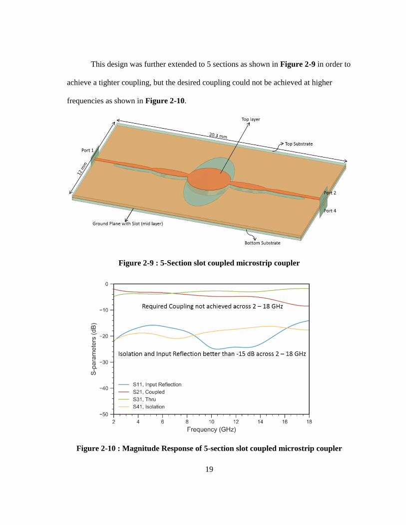
This design was further extended to 5 sections as shown in Figure 2-9 in order to
achieve a tighter coupling, but the desired coupling could not be achieved at higher
frequencies as shown in Figure 2-10.
Figure 2-9 : 5-Section slot coupled microstrip coupler
Figure 2-10 : Magnitude Response of 5-section slot coupled microstrip coupler
20
Another way to design a tight coupler is to connect two loose couplers in tandem.
By connecting two 8.34 dB couplers in tandem a tight coupling of 3 dB is achieved. This
can be shown using a similar analysis as done in Section 1.3. The S -matrix of first
hybrid coupler is,
[
𝟎 −𝒋 𝐜𝐨𝐬 𝜶𝟏 𝐬𝐢𝐧𝜶𝟏 𝟎−𝒋 𝐜𝐨𝐬 𝜶𝟏 𝟎 𝟎 𝐬𝐢𝐧𝜶𝟏
𝐬𝐢𝐧𝜶𝟏 𝟎 𝟎 −𝒋 𝐜𝐨𝐬𝜶𝟏
𝟎 𝐬𝐢𝐧𝜶𝟏 −𝒋 𝐜𝐨𝐬 𝜶𝟏 𝟎
] (2-15)
And similarly S-matrix of second hybrid coupler is given by
[
𝟎 −𝒋 𝐜𝐨𝐬 𝜶𝟐 𝐬𝐢𝐧𝜶𝟐 𝟎−𝒋 𝐜𝐨𝐬 𝜶𝟐 𝟎 𝟎 𝐬𝐢𝐧𝜶𝟐
𝐬𝐢𝐧𝜶𝟐 𝟎 𝟎 −𝒋 𝐜𝐨𝐬𝜶𝟐
𝟎 𝐬𝐢𝐧𝜶𝟐 −𝒋 𝐜𝐨𝐬 𝜶𝟐 𝟎
] (2-16)
Where 𝐬𝐢𝐧 𝜶𝟏 and 𝐬𝐢𝐧𝜶𝟐 are the voltage coupling coefficients of the two hybrid
couplers. When input port of the first coupler is excited by a wave voltage of amplitude
one, the reflected voltages obtained using the S-parameter are,
[
𝑽𝟏−
𝑽𝟐−
𝑽𝟑−
𝑽𝟒−
] = [
𝟎 −𝒋 𝐜𝐨𝐬 𝜶𝟏 𝐬𝐢𝐧𝜶𝟏 𝟎−𝒋 𝐜𝐨𝐬𝜶𝟏 𝟎 𝟎 𝐬𝐢𝐧𝜶𝟏
𝐬𝐢𝐧𝜶𝟏 𝟎 𝟎 −𝒋 𝐜𝐨𝐬 𝜶𝟏
𝟎 𝐬𝐢𝐧𝜶𝟏 −𝒋 𝐜𝐨𝐬 𝜶𝟏 𝟎
] [
𝟏𝟎𝟎𝟎
] (2-17)
𝑽𝟏− = 𝟎 (2-18)
𝑽𝟐− = −𝒋 𝐜𝐨𝐬 𝜶𝟏 (2-19)
𝑽𝟑− = 𝐬𝐢𝐧𝜶𝟏 (2-20)
𝑽𝟒− = 𝟎 (2-21)
For the second hybrid 𝑽𝟐− and 𝑽𝟑
− are the incident voltage waves at port 1 and port 4, and
using S-parameters of the second hybrid coupler,
21
[
𝑽𝟏′−
𝑽′𝟐−
𝑽′𝟑−
𝑽′𝟒−]
= [
𝟎 −𝒋 𝐜𝐨𝐬 𝜶𝟐 𝐬𝐢𝐧𝜶𝟐 𝟎−𝒋 𝐜𝐨𝐬 𝜶𝟐 𝟎 𝟎 𝐬𝐢𝐧𝜶𝟐
𝐬𝐢𝐧𝜶𝟐 𝟎 𝟎 −𝒋 𝐜𝐨𝐬 𝜶𝟐
𝟎 𝐬𝐢𝐧𝜶𝟐 −𝒋 𝐜𝐨𝐬𝜶𝟐 𝟎
] [
𝐬𝐢𝐧𝜶𝟏
𝟎𝟎
−𝒋 𝐜𝐨𝐬 𝜶𝟏
] (2-22)
𝑽′𝟏− = 𝟎 (2-23)
𝑽′𝟐− = −𝒋 𝐜𝐨𝐬 𝜶𝟐 𝐬𝐢𝐧 𝜶𝟏 − 𝒋 𝐬𝐢𝐧𝜶𝟐 𝐜𝐨𝐬 𝜶𝟏 = −𝒋 𝐬𝐢𝐧(𝜶𝟏 + 𝜶𝟐) (2-24)
𝑽′𝟑− = 𝐬𝐢𝐧𝜶𝟐 𝐬𝐢𝐧 𝜶𝟏 − 𝐜𝐨𝐬𝜶𝟐 𝐜𝐨𝐬𝜶𝟏 = − 𝐜𝐨𝐬(𝜶𝟏 + 𝜶𝟐) (2-25)
𝑽′𝟒− = 𝟎 (2-26)
If 𝜶𝟏 = 𝜶𝟐 = 𝝅
𝟖, 𝐬𝐢𝐧 (
𝝅
𝟖) = 0.3827 is the voltage coupling coefficient, which equals
−𝟐𝟎 𝐥𝐨𝐠(𝟎. 𝟐𝟖𝟐𝟕) = 𝟖. 𝟑𝟒 𝒅𝑩.
Using these values of voltage coupling coefficients,
𝑽′𝟐− = −𝒋 𝐬𝐢𝐧 (
𝝅
𝟖+
𝝅
𝟖) = −𝒋 𝐬𝐢𝐧 (
𝝅
𝟒) = −𝒋√ ½ (2-27)
𝑽′𝟑− = −𝒋 𝐜𝐨𝐬 (
𝝅
𝟖+
𝝅
𝟖) = −𝒋 𝐜𝐨𝐬 (
𝝅
𝟒) = −√ ½ (2-28)
which is equivalent to 3 dB coupling in terms of power.
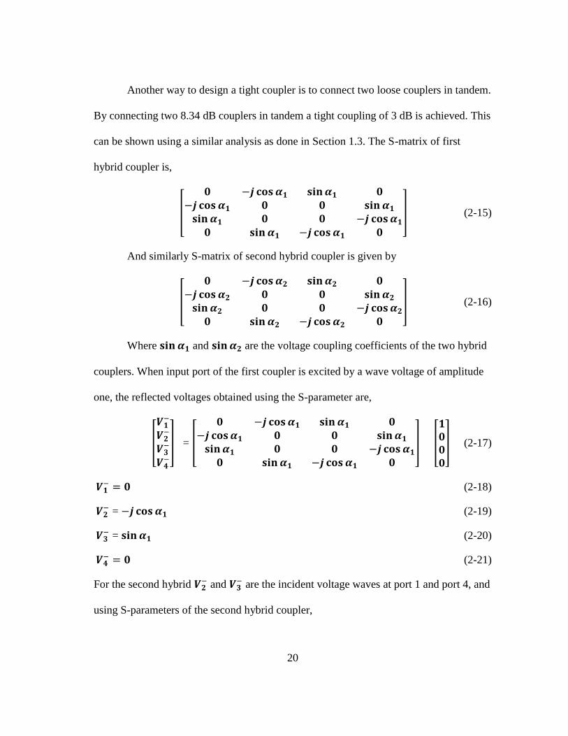
Figure 2-11 shows a block diagram of such a coupler.
Figure 2-11 : 3 dB coupler as a tandem connection of two 8.34 dB couplers
22
2.4. Coupler Design
For this work, two multi-section 8.34 dB couplers are designed and then
connected in tandem as discussed in the last section to achieve 3 dB or the hybrid
coupler.
The theoretical design equations and tables given in [15] were used as reference
for designing the 8.34 dB coupler. The work in [15] is based on finding an insertion loss
function which is unity plus square of an odd polynomial function which follows from
the previous work in [20]. Thus the theoretical design of a multi-section coupler reduces
to finding the optimum polynomial function followed by extracting the even and odd-
mode transmission-line impedances from the polynomial function. Following this
analysis, theoretical values of odd and even mode impedances have been tabulated in
[15] according to the required coupling coefficient, bandwidth and number of sections.
To minimize the area of design, least number of sections should be used. At the
same time ultra-wideband operation must be achieved. The required bandwidth of 2-18
GHz was achieved for 8.34 dB coupler using a symmetric 7-section design having
normalized even mode impedances 1.045, 1.122, 1.3014 and 2 Ohms. For a 50 Ohm
design, these are multiplied by 50 to get the even mode impedance to be realized. Odd
mode impedance can be calculated using [21],
𝒁𝟎𝟐 = 𝒁𝟎𝒆 𝒁𝟎𝒐 (2-29)
Where 𝒁𝟎 = 50 Ohms, 𝒁𝟎𝒆 and 𝒁𝟎𝒐 are even and odd mode impedances respectively.
The voltage coupling coefficient is given by, 𝒁𝟎𝒆− 𝒁𝟎𝒐
𝒁𝟎𝒆+ 𝒁𝟎𝒐 which is equivalent to
23
𝟐𝟎 𝐥𝐨𝐠 (𝒁𝟎𝒆− 𝒁𝟎𝒐
𝒁𝟎𝒆+ 𝒁𝟎𝒐) in dB. Using these equations even mode impedances for the
symmetric 7-section design are found to be 52.27, 56.10, 65.07 and 107.82 Ohms and
the odd mode impedances are 47.83, 44.56, 38.42 and 23.19 Ohms. The coupling factors
are 27.06 dB, 18.81 dB, 11.78 dB and 3.80 dB.
The 3.80 dB tight coupling is still hard to realize as edge coupled microstrip lines
as discussed in previous sections. Hence homogenous stripline structure has been
designed which also helps in maintaining equal odd and even mode phase velocities
since pure TEM mode propagates. The center section which requires tight coupling of
3.80 dB is designed as broadside coupled since it provides large area for coupling and
other six sections are designed as offset coupled. The geometries of broadside and offset
coupled striplines were shown in Figure 2-1.
The geometry of each section of stripline is decided according to the coupling
required. For broadside coupled striplines the even and odd mode characteristic
impedances are given by [22] (assuming negligible strip thickness),
𝒁𝟎𝒆 = 𝟔𝟎𝝅
√𝜺𝒓
𝑲′(𝒌)
𝑲 (𝒌) (2-30)
𝒁𝟎𝒐 = 𝟐𝟗𝟔.𝟏
√𝜺𝒓 𝒃
𝒔 𝒕𝒂𝒏𝒉−𝟏(𝒌)
(2-31)
where 𝑲 is complete elliptic function of the first kind, and 𝑲′ is the complementary
function given by,
𝑲′(𝒌) = 𝑲(𝒌′) = 𝑲 (√𝟏 − 𝒌𝟐) (2-32)
where k is related to the dimensions of the structure as follows:
𝑾
𝒃=
𝟏
𝝅[𝒍𝒏 (
𝟏+𝑹
𝟏−𝑹) −
𝑺
𝒃𝒍𝒏 (
𝟏+𝑹 𝒌⁄
𝟏−𝑹 𝒌⁄)] (2-33)
24
𝑹 = [(𝒌𝒃
𝑺− 𝟏)
𝟏
𝒌
𝒃
𝑺− 𝟏⁄ ]
𝟏/𝟐
(2-34)
where, 𝒃, 𝑾, 𝑺 are shown in Figure 2-1 (c).
For voltage coupling coefficient, 𝑪 and terminal characteristic impedance 𝒁𝟎,
the odd even mode characteristic impedance is be given by [19],
𝒁𝟎𝒆 = 𝒁𝟎 (𝟏+𝑪
𝟏−𝑪)𝟏/𝟐
(2-35)
𝒁𝟎𝒐 = 𝒁𝟎 (𝟏−𝑪
𝟏+𝑪)𝟏/𝟐
(2-36)
and,
𝑲
𝑲′=
𝟔𝟎𝝅
𝒁𝟎√𝜺𝒓(𝟏−𝑪
𝟏+𝑪)𝟏/𝟐
(2-37)
[23] presented formulas for 𝑲/𝑲′ can be used to calculate 𝒌 for given coupling and
substrate.
𝑲
𝑲′=
𝟏
𝝅𝒍𝒏 (𝟐
𝟏+√𝒌
𝟏−√𝒌) 𝒇𝒐𝒓 , 𝟎. 𝟕𝟎𝟕 < 𝒌 < 𝟏 (2-38)
𝑲
𝑲′=
𝝅
𝒍𝒏(𝟐𝟏+√𝒌′
𝟏−√𝒌′)
𝒇𝒐𝒓 , 𝟎. 𝟎 < 𝒌 < 𝟎. 𝟕𝟎𝟕 (2-39)
For 𝑲/𝑲′ > 1 or 𝑪 < (𝟏. 𝟎 − 𝑷𝜺𝒓)/(𝟏. 𝟎 + 𝑷𝜺𝒓), k is expressed as,
𝒌 = (𝟎.𝟓 𝒆(𝝅𝑲/𝑲′)−𝟏
𝟎.𝟓 𝒆(𝝅𝑲/𝑲′)−𝟏)𝟐
(2-40)
And for the case of 𝑲/𝑲′ < 1 or 𝑪 > (𝟏. 𝟎 − 𝑷𝜺𝒓)/(𝟏. 𝟎 + 𝑷𝜺𝒓), k is expressed as,
𝒌 = [𝟏 − (𝟎.𝟓 𝒆(𝝅𝑲′/𝑲)−𝟏
𝟎.𝟓 𝒆(𝝅𝑲′/𝑲)−𝟏)𝟒
]
𝟏/𝟐
(2-41)
where 𝑷 = (𝒁𝟎/𝟔𝟎𝝅)𝟐 and in the geometry the ratio,
𝑺
𝒃= 𝟎. 𝟎𝟎𝟏𝟕 𝒁𝟎√𝜺𝒓 (
𝟏−𝑪
𝟏+𝑪)𝟏/𝟐
𝒍𝒏𝟏+𝒌
𝟏−𝒌 (2-42)
25
These elliptical integrals can also be evaluated in Python. For given C, 𝜺𝒓 and 𝒁𝟎
the geometry ratios W/b and S/b can be calculated using these equations. Stripline
calculators can also be used to instead of solving these equations.
Analysis for offset coupled lines has been given in [24], which is skipped
because modern stripline calculators can be used to find the geometries of the coupled
lines according to the coupling requirement or the even and odd mode impedances.
Although the tables and equations can theoretically design any coupler but for a
physically realizable structure the spacing ‘s’ in Figure 2-1 should be uniform
throughout for each section and at the same time the widths ‘w’ and spacing ‘wc’ should
not be too large or too small. Such constraints were satisfied by diligently selecting
substrate type and designing the stripline structure. Duroid 4003 (εr = 3.55) is used as
substrate in this work which satisfied the above constraints. Using equations mentioned
in this section, even odd mode impedances are calculated for each section and using the
equations or calculators the geometry of each section was calculated for Duroid 4003.
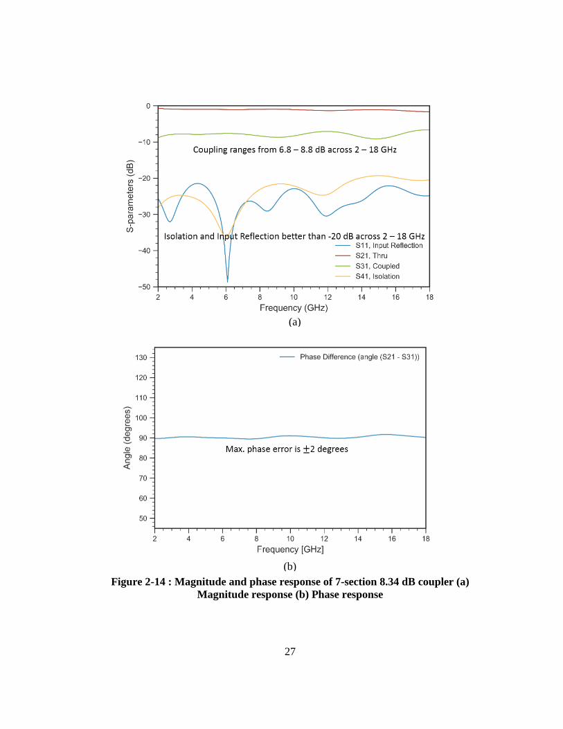
Figure 2-12 shows the designed 7-section symmetric 8.34 dB coupler, with
center section as broadside coupled and the 6 sections as offset coupled striplines.
Magnitude and phase response is shown in Figure 2-14. Figure 2-13 highlights the
generic stripline structure that will be followed for all the further designs discussed in
this thesis.
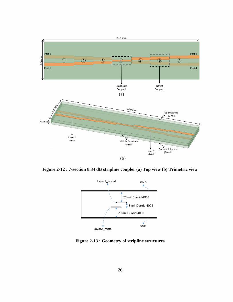
26
Figure 2-12 : 7-section 8.34 dB stripline coupler (a) Top view (b) Trimetric view
Figure 2-13 : Geometry of stripline structures
(a)
(b)
27
Figure 2-14 : Magnitude and phase response of 7-section 8.34 dB coupler (a)
Magnitude response (b) Phase response
(a)
(b)
28
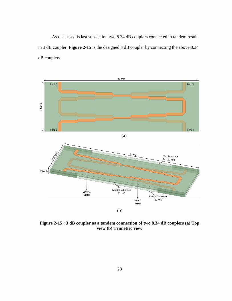
As discussed is last subsection two 8.34 dB couplers connected in tandem result
in 3 dB coupler. Figure 2-15 is the designed 3 dB coupler by connecting the above 8.34
dB couplers.
Figure 2-15 : 3 dB coupler as a tandem connection of two 8.34 dB couplers (a) Top
view (b) Trimetric view
(a)
(b)
29
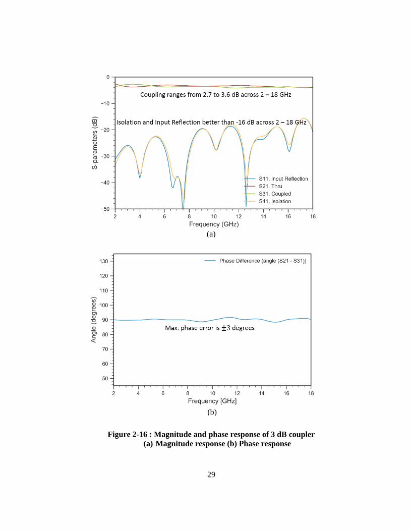
Figure 2-16 : Magnitude and phase response of 3 dB coupler
(a) Magnitude response (b) Phase response
(b)
(a)
30
Figure 2-16 (a) shows it achieves tight coupling varying from 2.5 dB to 3.6 dB
across 2-18 GHz range. Figure 2-16 (b) shows the phase difference between the through
and coupled ports which is 90° with an error of ±3°.
Similar coupler was designed in [25], with 41 sections (97 mm x 46 mm) for 0.5-
18 Ghz. The simulated results in [25] show coupling lowers as the frequency increases,
with 5 dB coupling at 18 GHz. In this work tight coupling (2.6 dB to 3.7 dB) is achieved
for 2-18 GHz with much smaller size (31.78 mm x 9.78 mm).
31
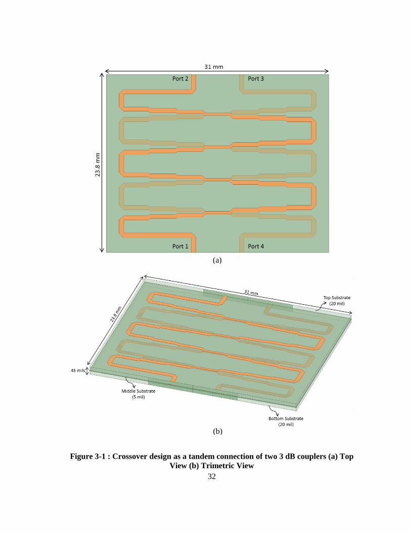
3. CROSSOVER DESIGN
This brief section covers the design of crossover required for Butler Matrix. As
discussed in Section 1.3 crossover is designed by connecting two 3 dB couplers in
tandem. Figure 3-1 shows such a crossover design in HFSS. Extra line lengths are added
to assist in layout of Butler Matrix later.
Although the physical size of the crossover is small, but the electrical size is too
large considering the highest frequency of operation is 18 GHz. Moreover the
simulations need to run from 2 to 18 GHz to analyze the design over the full bandwidth.
For running finite element method simulations in HFSS, such a design requires large
computational resources. Therefore these simulations were run on supercomputing
cluster, Texas A&M High Performance Research Computing (HPRC).
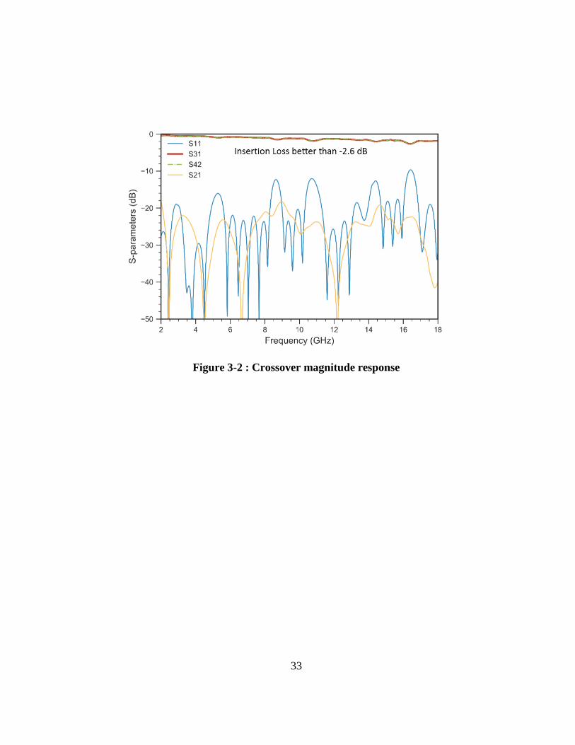
Figure 3-2 shows its magnitude response. Ideally all the input power should be
present at output but due to long length of transmission lines we see maximum insertion
loss of -2.6 dB.
32
Figure 3-1 : Crossover design as a tandem connection of two 3 dB couplers (a) Top
View (b) Trimetric View
(a)
(b)
33
Figure 3-2 : Crossover magnitude response
34
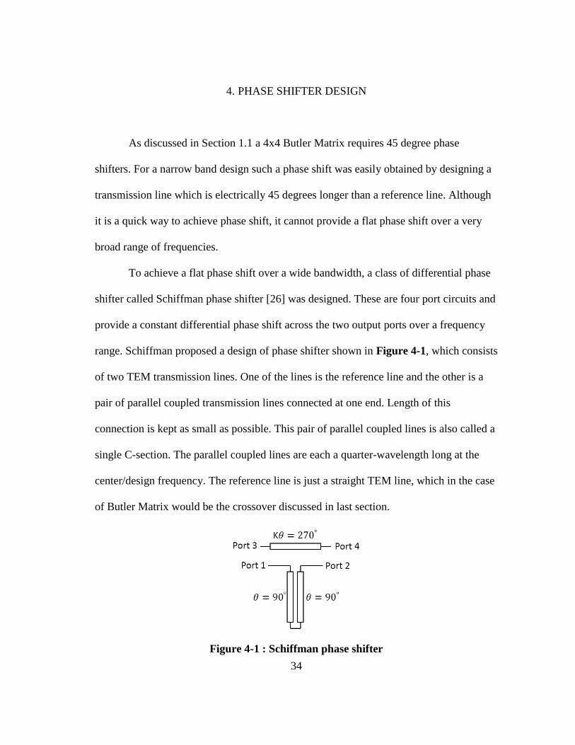
4. PHASE SHIFTER DESIGN
As discussed in Section 1.1 a 4x4 Butler Matrix requires 45 degree phase
shifters. For a narrow band design such a phase shift was easily obtained by designing a
transmission line which is electrically 45 degrees longer than a reference line. Although
it is a quick way to achieve phase shift, it cannot provide a flat phase shift over a very
broad range of frequencies.
To achieve a flat phase shift over a wide bandwidth, a class of differential phase
shifter called Schiffman phase shifter [26] was designed. These are four port circuits and
provide a constant differential phase shift across the two output ports over a frequency
range. Schiffman proposed a design of phase shifter shown in Figure 4-1, which consists
of two TEM transmission lines. One of the lines is the reference line and the other is a
pair of parallel coupled transmission lines connected at one end. Length of this
connection is kept as small as possible. This pair of parallel coupled lines is also called a
single C-section. The parallel coupled lines are each a quarter-wavelength long at the
center/design frequency. The reference line is just a straight TEM line, which in the case
of Butler Matrix would be the crossover discussed in last section.
Figure 4-1 : Schiffman phase shifter
35
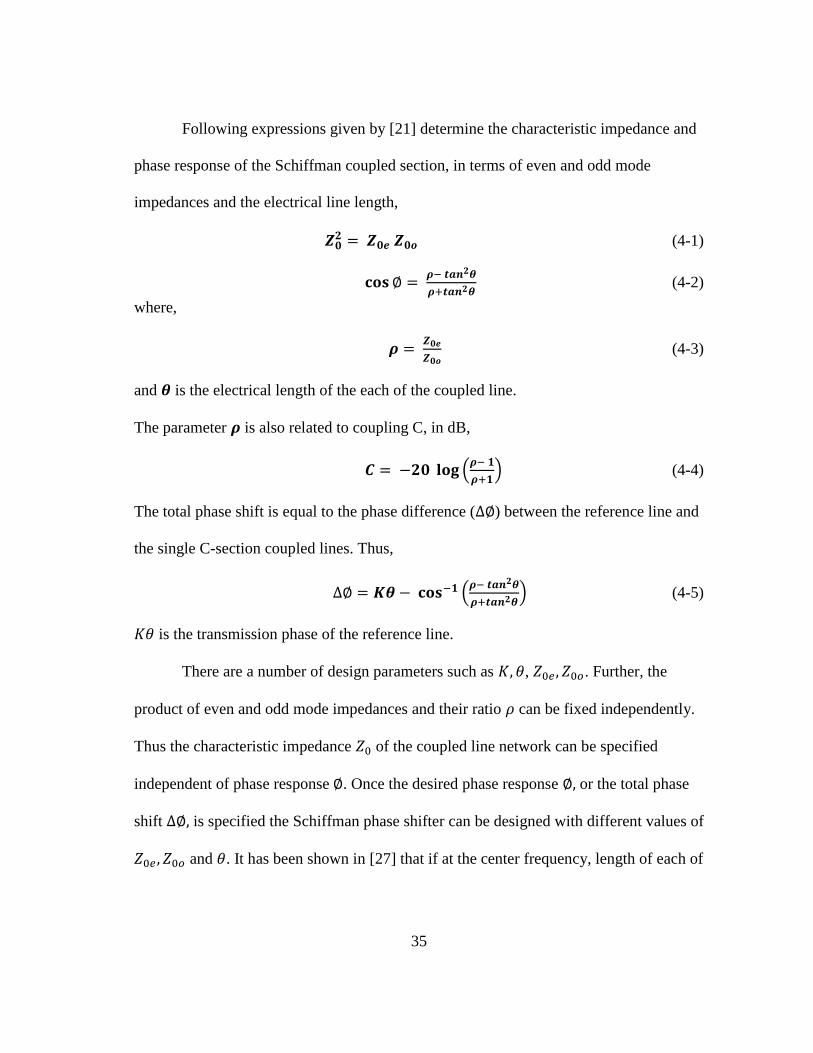
Following expressions given by [21] determine the characteristic impedance and
phase response of the Schiffman coupled section, in terms of even and odd mode
impedances and the electrical line length,
𝒁𝟎𝟐 = 𝒁𝟎𝒆 𝒁𝟎𝒐 (4-1)
𝐜𝐨𝐬 ∅ = 𝝆− 𝒕𝒂𝒏𝟐𝜽
𝝆+𝒕𝒂𝒏𝟐𝜽 (4-2)
where,
𝝆 = 𝒁𝟎𝒆
𝒁𝟎𝒐 (4-3)
and 𝜽 is the electrical length of the each of the coupled line.
The parameter 𝝆 is also related to coupling C, in dB,
𝑪 = −𝟐𝟎 𝐥𝐨𝐠 (𝝆− 𝟏
𝝆+𝟏) (4-4)
The total phase shift is equal to the phase difference (∆∅) between the reference line and
the single C-section coupled lines. Thus,
∆∅ = 𝑲𝜽 − 𝐜𝐨𝐬−𝟏 (𝝆− 𝒕𝒂𝒏𝟐𝜽
𝝆+𝒕𝒂𝒏𝟐𝜽) (4-5)
𝐾𝜃 is the transmission phase of the reference line.
There are a number of design parameters such as 𝐾, 𝜃, 𝑍0𝑒 , 𝑍0𝑜. Further, the
product of even and odd mode impedances and their ratio 𝜌 can be fixed independently.
Thus the characteristic impedance 𝑍0 of the coupled line network can be specified
independent of phase response ∅. Once the desired phase response ∅, or the total phase
shift ∆∅, is specified the Schiffman phase shifter can be designed with different values of
𝑍0𝑒 , 𝑍0𝑜 and 𝜃. It has been shown in [27] that if at the center frequency, length of each of
36
the coupled line equals quarter wavelength or 𝜃 = 𝜋 2⁄ , then the phase shift ∆∅ is anti-
symmetric around the center frequency, which leads to the broadest bandwidth.
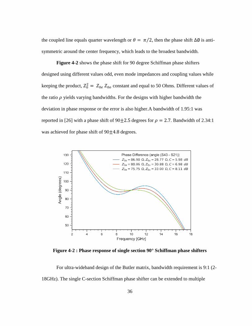
Figure 4-2 shows the phase shift for 90 degree Schiffman phase shifters
designed using different values odd, even mode impedances and coupling values while
keeping the product, 𝑍02 = 𝑍0𝑒 𝑍0𝑜 constant and equal to 50 Ohms. Different values of
the ratio 𝜌 yields varying bandwidths. For the designs with higher bandwidth the
deviation in phase response or the error is also higher.A bandwidth of 1.95:1 was
reported in [26] with a phase shift of 90±2.5 degrees for 𝜌 = 2.7. Bandwidth of 2.34:1
was achieved for phase shift of 90±4.8 degrees.
Figure 4-2 : Phase response of single section 90° Schiffman phase shifters
For ultra-wideband design of the Butler matrix, bandwidth requirement is 9:1 (2-
18GHz). The single C-section Schiffman phase shifter can be extended to multiple
37
sections of coupled lines to increase bandwidth over which the phase shift is flat.
Analysis for this was done in [28]. The equations extend from the phase response of the
single section. For ‘n’ sections of coupled line in a Schiffman phase shifter the phase
response is given by,
𝐜𝐨𝐬 ∅𝒏 = 𝝆𝟏− 𝒕𝒂𝒏𝟐𝜽′𝟏
𝝆𝟏+𝒕𝒂𝒏𝟐𝜽′𝟏(4-6)
where,
𝜽′𝟏 = 𝜽𝟏 + 𝐭𝐚𝐧−𝟏(𝝆𝟏𝟐 𝐭𝐚𝐧 𝜽′𝟐) (4-7)
𝜽′𝟐 = 𝜽𝟐 + 𝐭𝐚𝐧−𝟏(𝝆𝟐𝟑 𝐭𝐚𝐧 𝜽′𝟑) (4-8)
.
.
𝜽′𝒏−𝟏 = 𝜽𝒏−𝟏 + 𝐭𝐚𝐧−𝟏(𝝆𝒏−𝟏,𝒏 𝐭𝐚𝐧 𝜽′𝒏) (4-9)
𝜽′𝒏 = 𝜽𝒏 (4-10)
and
𝝆𝒊,𝒊+𝟏 = 𝒁𝟎𝒆 𝒊
𝒁𝟎𝒆 (𝒊+𝟏)=
𝒁𝟎𝒐 (𝒊+𝟏)
𝒁𝟎𝒐 𝒊 (4-11)
While 𝑍02 = 𝑍0𝑒 𝑖 𝑍0𝑜 𝑖 is true for each section.
As in the case of multi-section hybrid coupler, the equations result in a
theoretical design which may or may not be physically realizable. Using the same
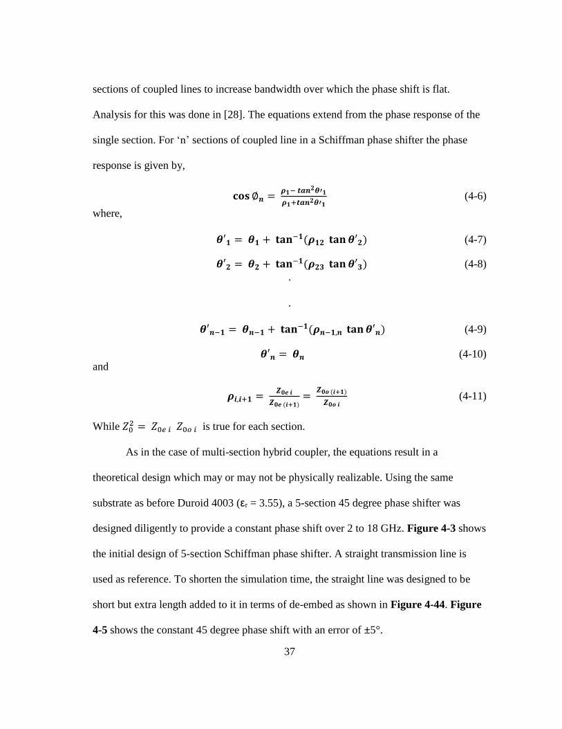
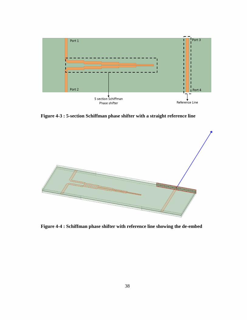
substrate as before Duroid 4003 (εr = 3.55), a 5-section 45 degree phase shifter was
designed diligently to provide a constant phase shift over 2 to 18 GHz. Figure 4-3 shows
the initial design of 5-section Schiffman phase shifter. A straight transmission line is
used as reference. To shorten the simulation time, the straight line was designed to be
short but extra length added to it in terms of de-embed as shown in Figure 4-44. Figure
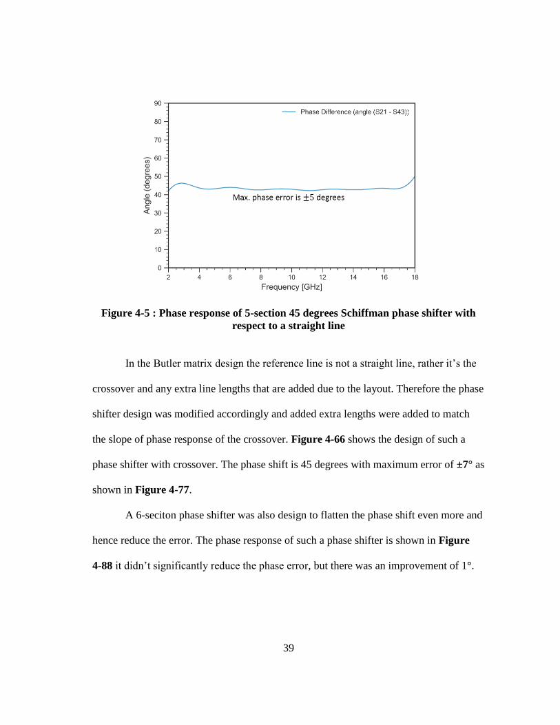
4-5 shows the constant 45 degree phase shift with an error of ±5°.
38
Figure 4-3 : 5-section Schiffman phase shifter with a straight reference line
Figure 4-4 : Schiffman phase shifter with reference line showing the de-embed
39
Figure 4-5 : Phase response of 5-section 45 degrees Schiffman phase shifter with
respect to a straight line
In the Butler matrix design the reference line is not a straight line, rather it’s the
crossover and any extra line lengths that are added due to the layout. Therefore the phase
shifter design was modified accordingly and added extra lengths were added to match
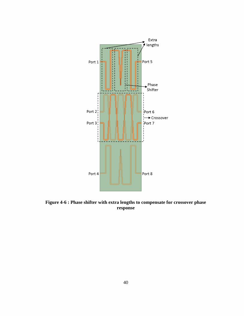
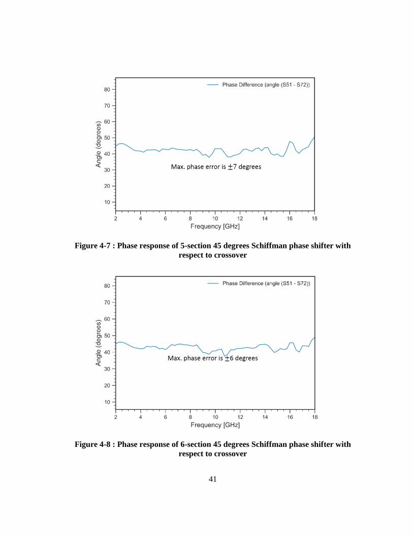
the slope of phase response of the crossover. Figure 4-66 shows the design of such a
phase shifter with crossover. The phase shift is 45 degrees with maximum error of ±7° as
shown in Figure 4-77.
A 6-seciton phase shifter was also design to flatten the phase shift even more and
hence reduce the error. The phase response of such a phase shifter is shown in Figure
4-88 it didn’t significantly reduce the phase error, but there was an improvement of 1°.
40
Figure 4-6 : Phase shifter with extra lengths to compensate for crossover phase
response
41
Figure 4-7 : Phase response of 5-section 45 degrees Schiffman phase shifter with
respect to crossover
Figure 4-8 : Phase response of 6-section 45 degrees Schiffman phase shifter with
respect to crossover
42
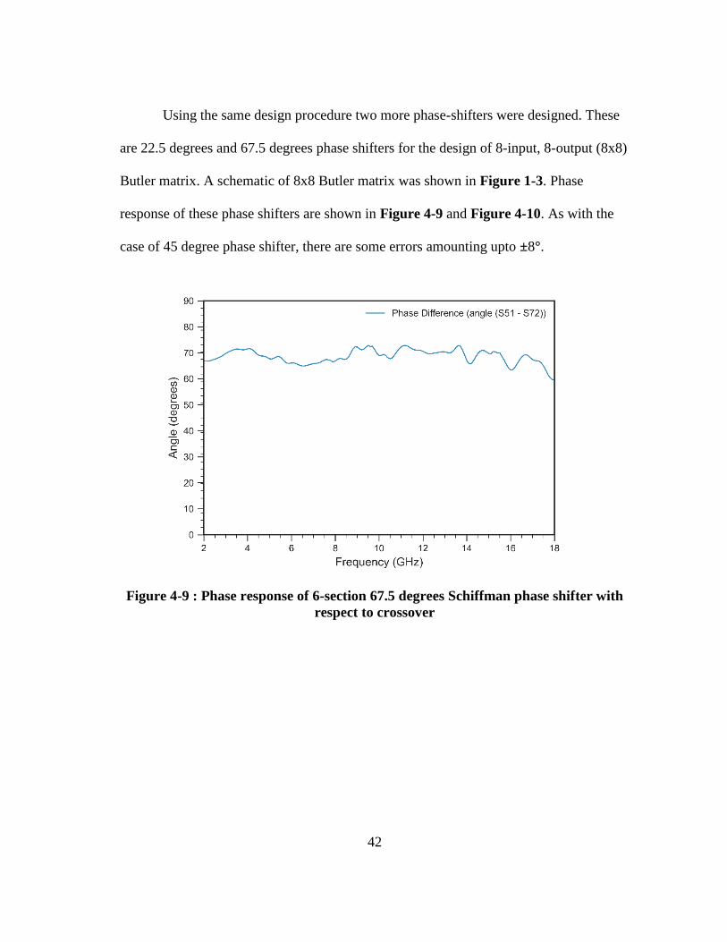
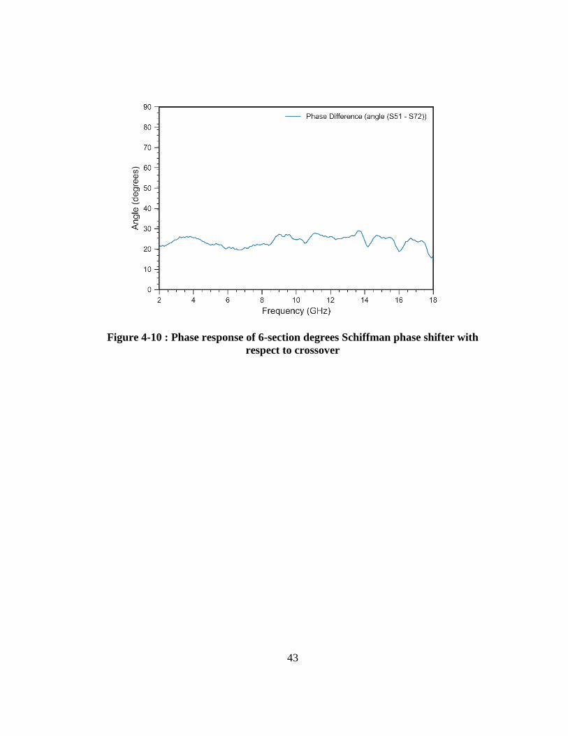
Using the same design procedure two more phase-shifters were designed. These
are 22.5 degrees and 67.5 degrees phase shifters for the design of 8-input, 8-output (8x8)
Butler matrix. A schematic of 8x8 Butler matrix was shown in Figure 1-3. Phase
response of these phase shifters are shown in Figure 4-9 and Figure 4-10. As with the
case of 45 degree phase shifter, there are some errors amounting upto ±8°.
Figure 4-9 : Phase response of 6-section 67.5 degrees Schiffman phase shifter with
respect to crossover
43
Figure 4-10 : Phase response of 6-section degrees Schiffman phase shifter with
respect to crossover
44
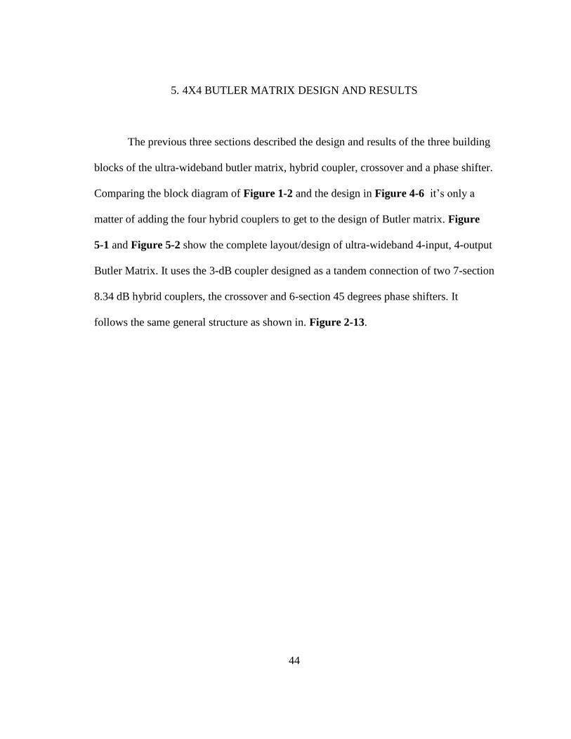
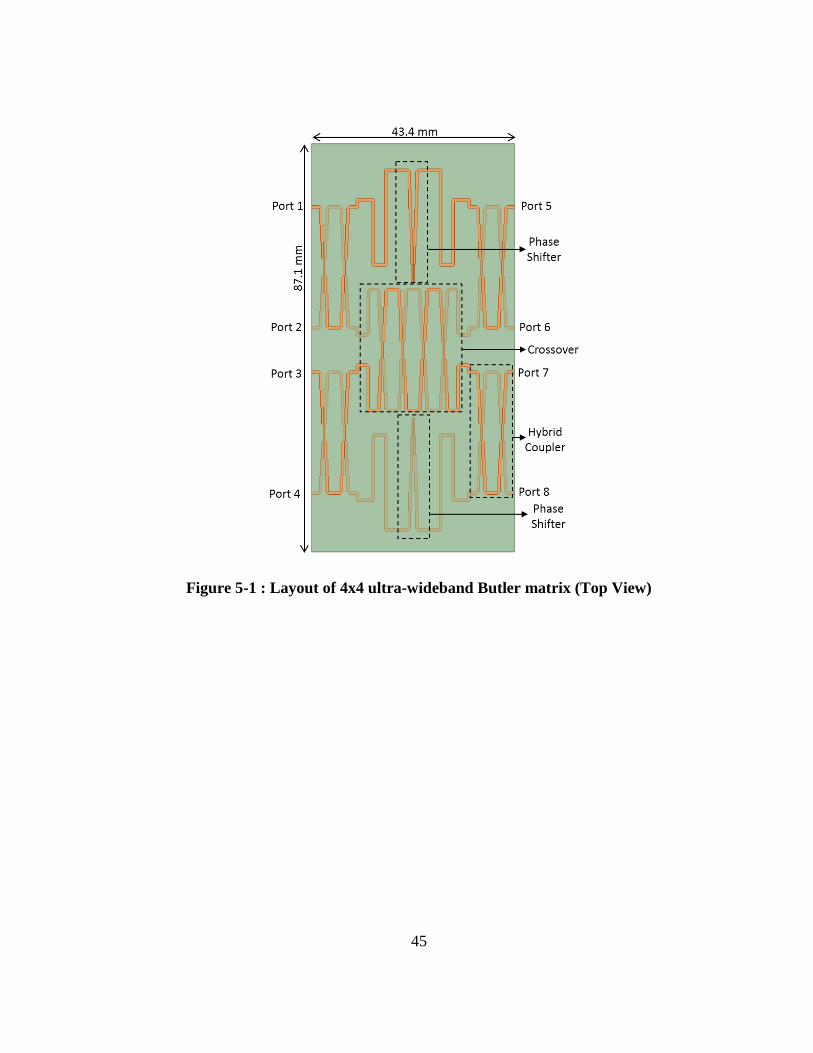
5. 4X4 BUTLER MATRIX DESIGN AND RESULTS
The previous three sections described the design and results of the three building
blocks of the ultra-wideband butler matrix, hybrid coupler, crossover and a phase shifter.
Comparing the block diagram of Figure 1-2 and the design in Figure 4-6 it’s only a
matter of adding the four hybrid couplers to get to the design of Butler matrix. Figure
5-1 and Figure 5-2 show the complete layout/design of ultra-wideband 4-input, 4-output
Butler Matrix. It uses the 3-dB coupler designed as a tandem connection of two 7-section
8.34 dB hybrid couplers, the crossover and 6-section 45 degrees phase shifters. It
follows the same general structure as shown in. Figure 2-13.
45
Figure 5-1 : Layout of 4x4 ultra-wideband Butler matrix (Top View)
46
Figure 5-2 : Layout of ultra-wideband Butler matrix (Trimetric view)
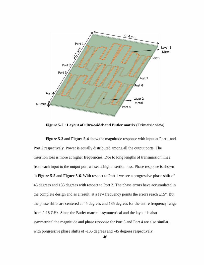
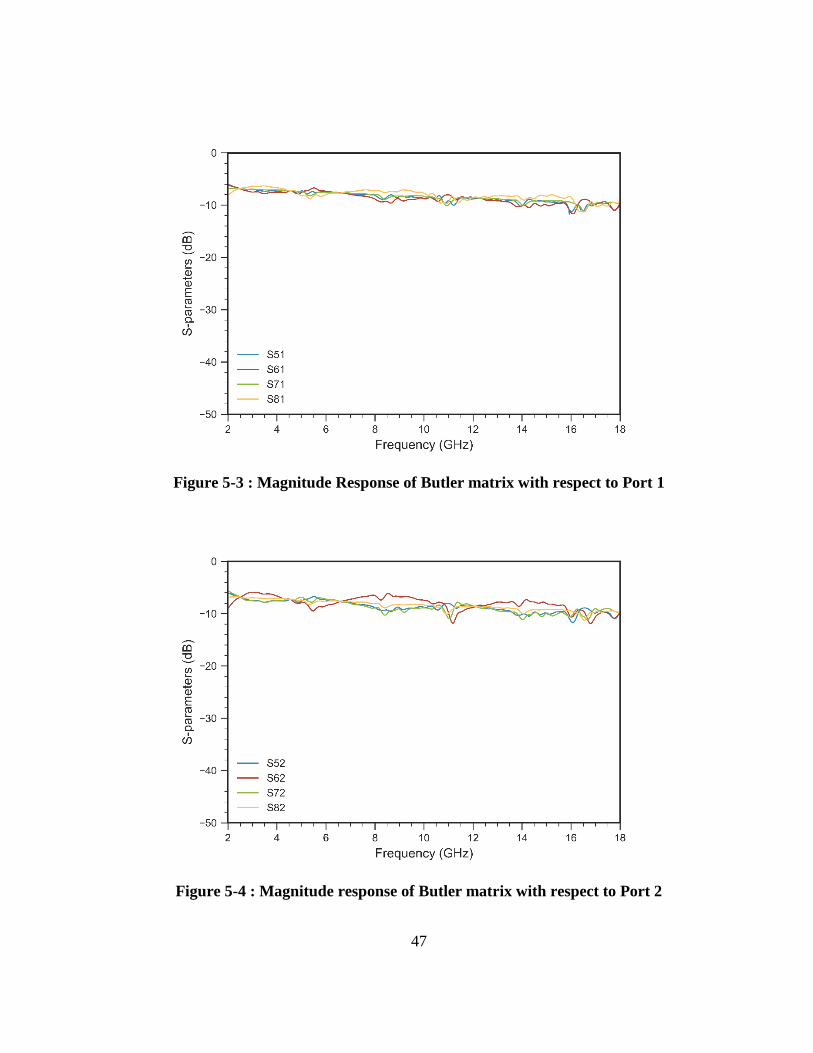
Figure 5-3 and Figure 5-4 show the magnitude response with input at Port 1 and
Port 2 respectively. Power is equally distributed among all the output ports. The
insertion loss is more at higher frequencies. Due to long lengths of transmission lines
from each input to the output port we see a high insertion loss. Phase response is shown
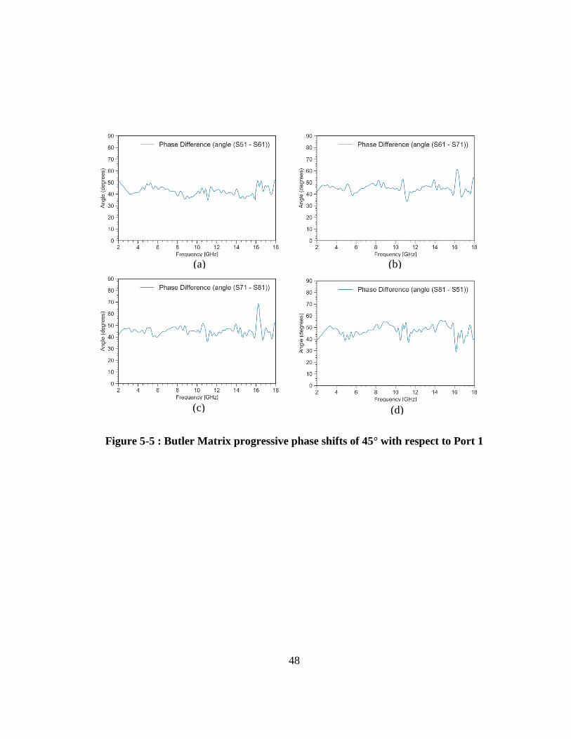
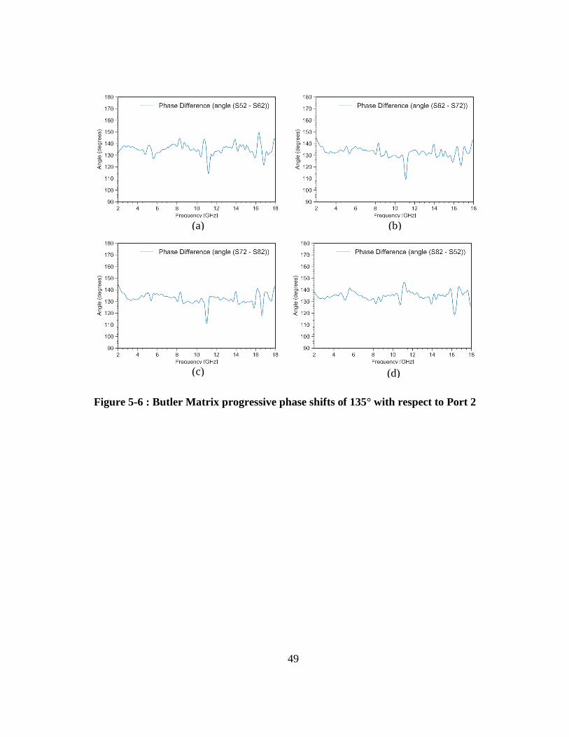
in Figure 5-5 and Figure 5-6. With respect to Port 1 we see a progressive phase shift of
45 degrees and 135 degrees with respect to Port 2. The phase errors have accumulated in
the complete design and as a result, at a few frequency points the errors reach ±15°. But
the phase shifts are centered at 45 degrees and 135 degrees for the entire frequency range
from 2-18 GHz. Since the Butler matrix is symmetrical and the layout is also
symmetrical the magnitude and phase response for Port 3 and Port 4 are also similar,
with progressive phase shifts of -135 degrees and -45 degrees respectively.
47
Figure 5-3 : Magnitude Response of Butler matrix with respect to Port 1
Figure 5-4 : Magnitude response of Butler matrix with respect to Port 2
48
Figure 5-5 : Butler Matrix progressive phase shifts of 45° with respect to Port 1
(a) (b)
(c) (d)
49
Figure 5-6 : Butler Matrix progressive phase shifts of 135° with respect to Port 2
(c)
(a) (b)
(d)
6. FUTURE WORK
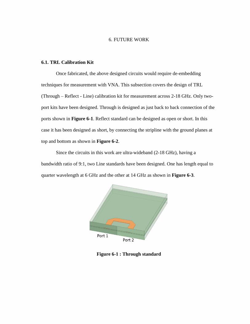
6.1. TRL Calibration Kit
Once fabricated, the above designed circuits would require de-embedding
techniques for measurement with VNA. This subsection covers the design of TRL
(Through – Reflect - Line) calibration kit for measurement across 2-18 GHz. Only two-
port kits have been designed. Through is designed as just back to back connection of the
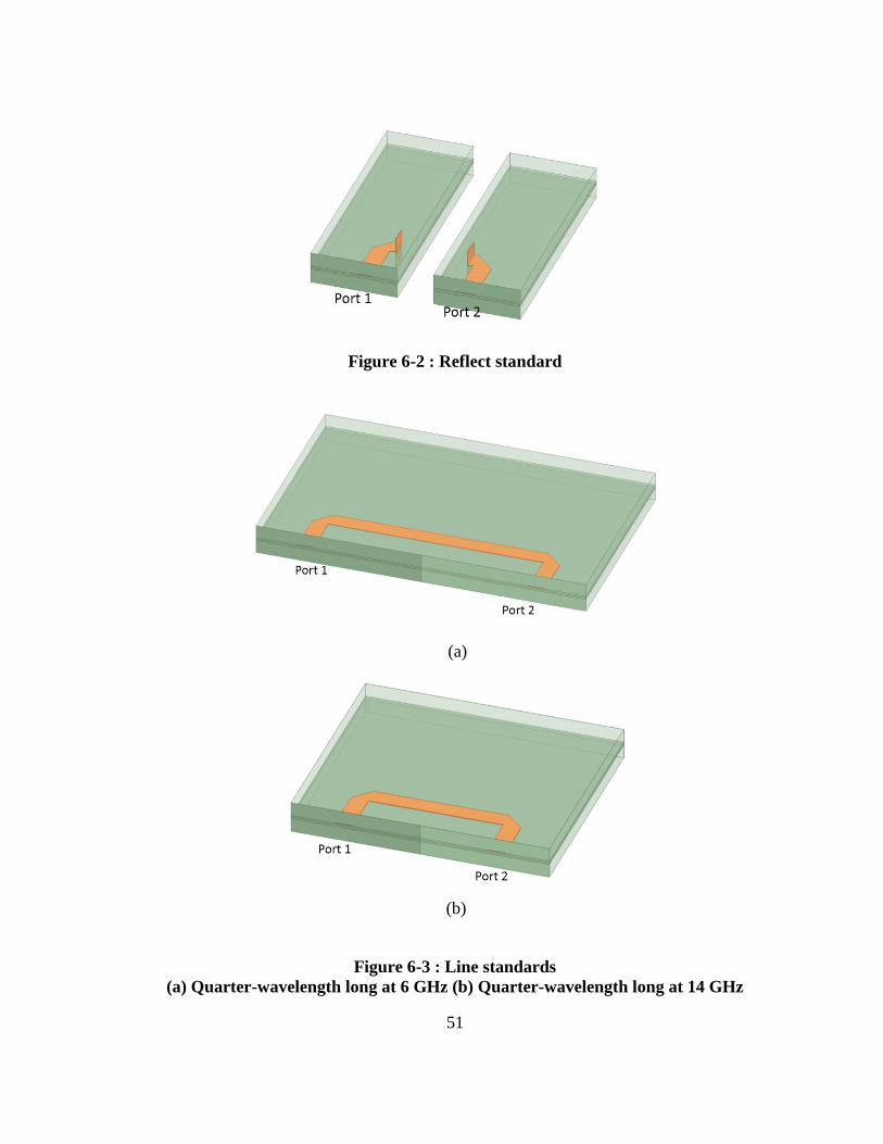
ports shown in Figure 6-1. Reflect standard can be designed as open or short. In this
case it has been designed as short, by connecting the stripline with the ground planes at
top and bottom as shown in Figure 6-2.
Since the circuits in this work are ultra-wideband (2-18 GHz), having a
bandwidth ratio of 9:1, two Line standards have been designed. One has length equal to
quarter wavelength at 6 GHz and the other at 14 GHz as shown in Figure 6-3.
Figure 6-1 : Through standard
51
Figure 6-2 : Reflect standard
Figure 6-3 : Line standards
(a) Quarter-wavelength long at 6 GHz (b) Quarter-wavelength long at 14 GHz
(a)
(b)
52
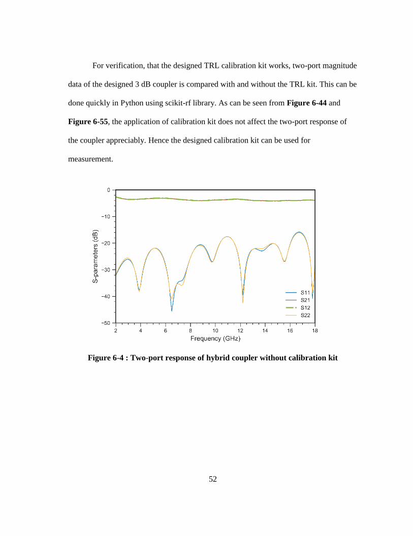
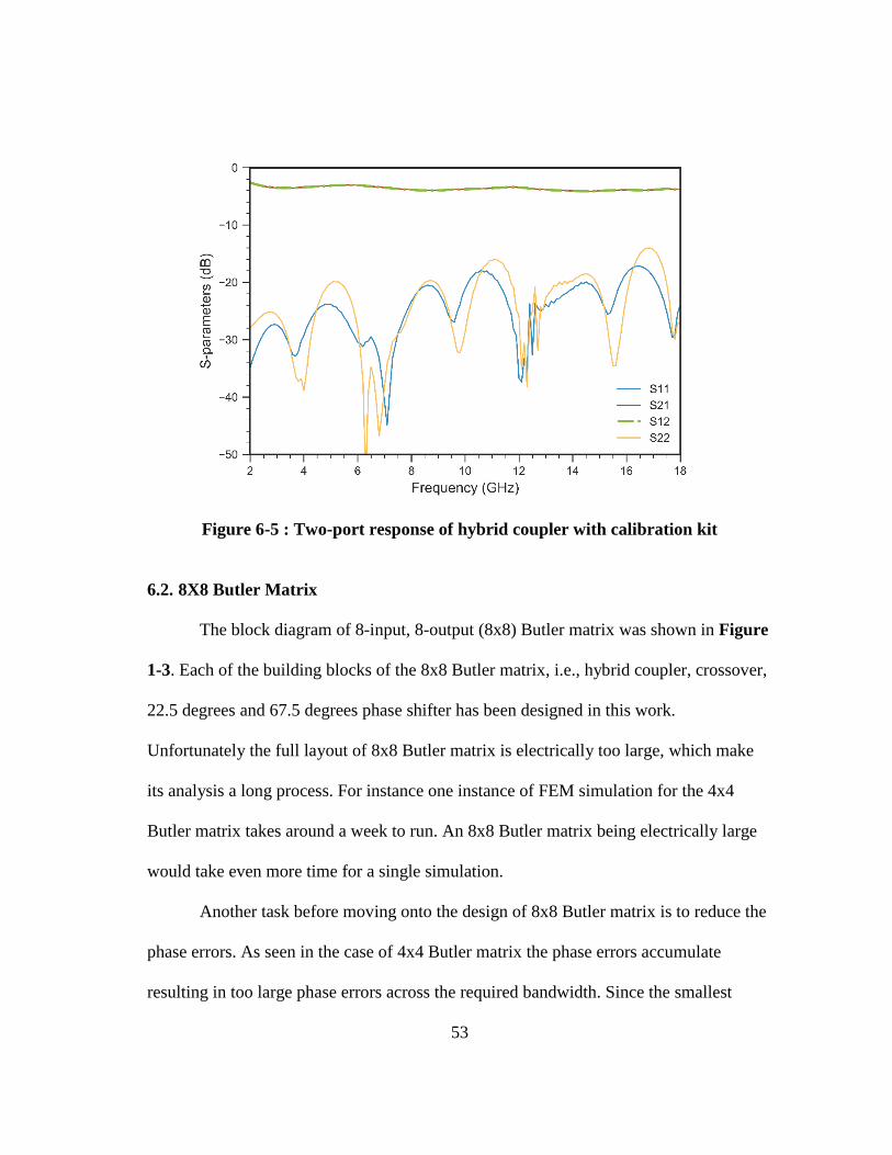
For verification, that the designed TRL calibration kit works, two-port magnitude
data of the designed 3 dB coupler is compared with and without the TRL kit. This can be
done quickly in Python using scikit-rf library. As can be seen from Figure 6-44 and
Figure 6-55, the application of calibration kit does not affect the two-port response of
the coupler appreciably. Hence the designed calibration kit can be used for
measurement.
Figure 6-4 : Two-port response of hybrid coupler without calibration kit
53
Figure 6-5 : Two-port response of hybrid coupler with calibration kit
6.2. 8X8 Butler Matrix
The block diagram of 8-input, 8-output (8x8) Butler matrix was shown in Figure
1-3. Each of the building blocks of the 8x8 Butler matrix, i.e., hybrid coupler, crossover,
22.5 degrees and 67.5 degrees phase shifter has been designed in this work.
Unfortunately the full layout of 8x8 Butler matrix is electrically too large, which make
its analysis a long process. For instance one instance of FEM simulation for the 4x4
Butler matrix takes around a week to run. An 8x8 Butler matrix being electrically large
would take even more time for a single simulation.
Another task before moving onto the design of 8x8 Butler matrix is to reduce the
phase errors. As seen in the case of 4x4 Butler matrix the phase errors accumulate
resulting in too large phase errors across the required bandwidth. Since the smallest
54
progressive phase shift for an 8x8 Butler matrix is 22.5 degrees, phase errors need to be
reduced in the full design.
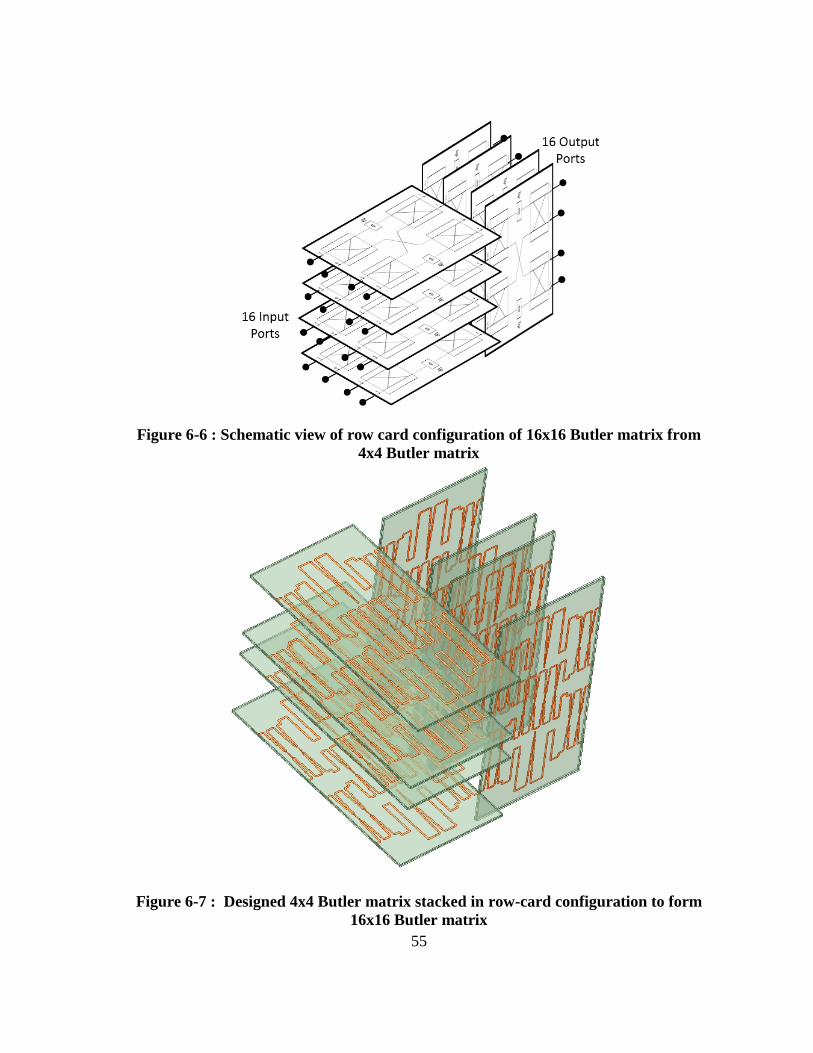
6.3. 16X16 Butler Matrix
The layout of 16-input, 16-output Butler matrix can get too tedious if same
approach is followed as for 4x4 and 8x8 Butler matrices. Moreover the board size would
be too large. Another way to design 16x16 Butler matrix is to use a row card
configuration as shown schematically in Figure 6-6. Each board is a 4x4 Butler matrix.
Figure 6-7 shows how this configuration would look like with the actual design.
Inputs are on the side where each 4x4 board is oriented horizontally and outputs
are on the vertical side. The first output port of each of the 4x4 horizontal board is
connected to the 4 inputs of the first 4x4 vertical board. Similarly the second output port
of each of the horizontal board is connected to the inputs of the second vertical board
and so on.
55
Figure 6-6 : Schematic view of row card configuration of 16x16 Butler matrix from
4x4 Butler matrix
Figure 6-7 : Designed 4x4 Butler matrix stacked in row-card configuration to form
16x16 Butler matrix
56
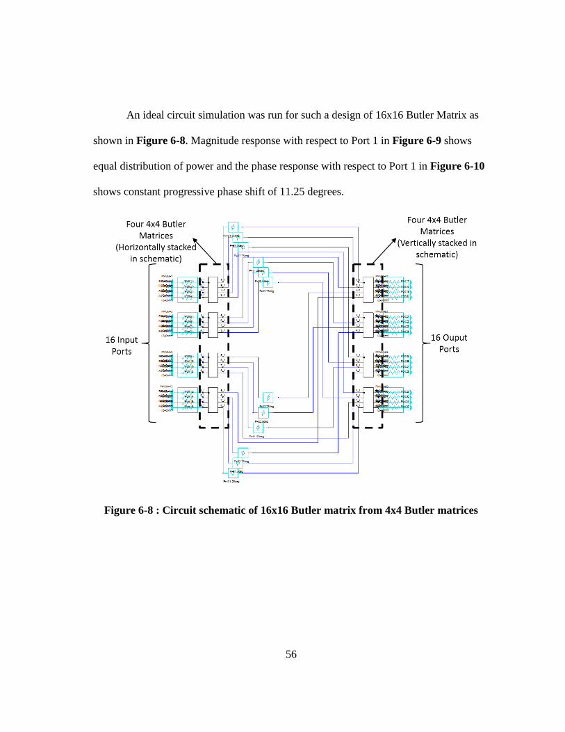
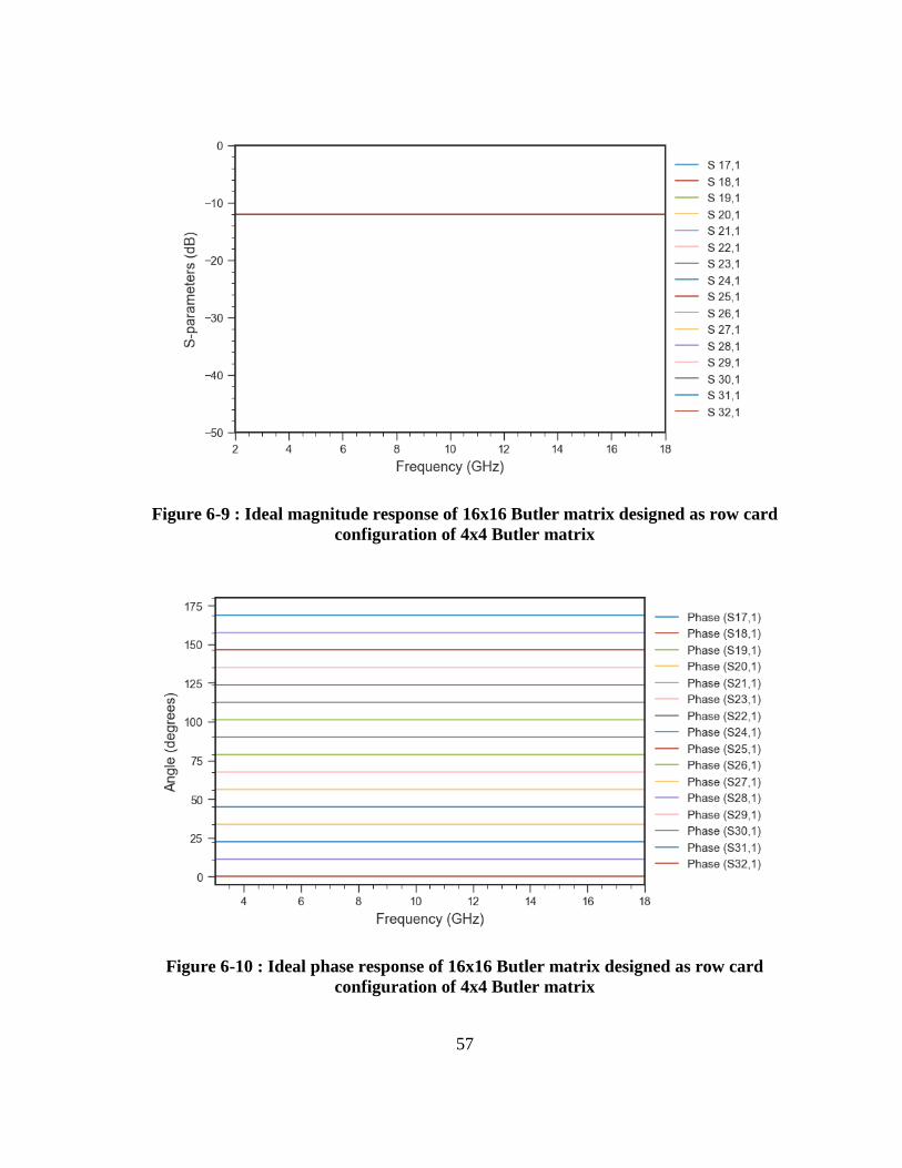
An ideal circuit simulation was run for such a design of 16x16 Butler Matrix as
shown in Figure 6-8. Magnitude response with respect to Port 1 in Figure 6-9 shows
equal distribution of power and the phase response with respect to Port 1 in Figure 6-10
shows constant progressive phase shift of 11.25 degrees.
Figure 6-8 : Circuit schematic of 16x16 Butler matrix from 4x4 Butler matrices
57
Figure 6-9 : Ideal magnitude response of 16x16 Butler matrix designed as row card
configuration of 4x4 Butler matrix
Figure 6-10 : Ideal phase response of 16x16 Butler matrix designed as row card
configuration of 4x4 Butler matrix
58
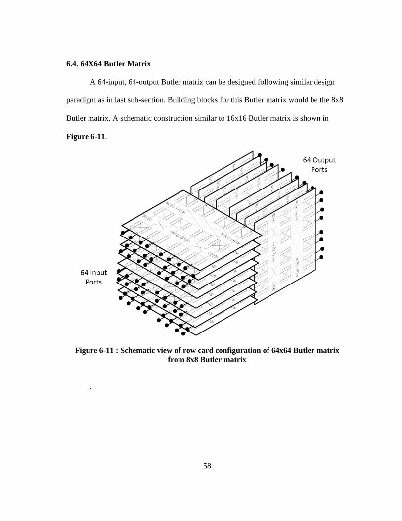
6.4. 64X64 Butler Matrix
A 64-input, 64-output Butler matrix can be designed following similar design
paradigm as in last sub-section. Building blocks for this Butler matrix would be the 8x8
Butler matrix. A schematic construction similar to 16x16 Butler matrix is shown in
Figure 6-11.
Figure 6-11 : Schematic view of row card configuration of 64x64 Butler matrix
from 8x8 Butler matrix
.

59
7. CONCLUSIONS
Design of ultra-wideband hybrid coupler, crossover and phase shifters has been
presented in this thesis, as a requirement for the design of ultra-wideband Butler matrix.
Hybrid coupler achieves tight coupling of 2.6 dB to 3.7 dB across the required
bandwidth of 2-18 GHz with a phase error of ± 3 degrees between the coupled and
through port. The hybrid coupler is extremely small in terms of physical size (3.1mm x
9.8 mm) as compared to previously designed coupler for such an ultra-wideband range.
The phase shifter has been designed as a multi-section Schiffman phase shifter which
was shown to have a constant phase shift of 45 degrees across 2-18 GHz with phase
error of ± 5 degrees.
Using the designed hybrid coupler, crossover and phase shifter an ultra-wideband
4-input, 4-output (4x4) Butler matrix has been designed and phase response shows
progressive phase shifts.
This work also lays down the foundation for the designs of ultra-wideband 8x8,
16x16 and 64x64 Butler matrices.

60
REFERENCES
1. Bekkerman, I. and J. Tabrikian, Target Detection and Localization Using MIMO
Radars and Sonars %J Trans. Sig. Proc. 2006. 54(10): p. 3873-3883.
2. Khan, R., et al., Target detection and tracking with a high frequency ground
wave radar. IEEE Journal of Oceanic Engineering, 1994. 19(4): p. 540-548.
3. Rahimian, A., Microwave Beamforming Networks for Intelligent Transportation
Systems. 2012.
4. Rashid-Farrokhi, F., K.J.R. Liu, and L. Tassiulas, Transmit beamforming and
power control for cellular wireless systems. IEEE Journal on Selected Areas in
Communications, 1998. 16(8): p. 1437-1450.
5. Roh, W., et al., Millimeter-wave beamforming as an enabling technology for 5G
cellular communications: theoretical feasibility and prototype results. IEEE
Communications Magazine, 2014. 52(2): p. 106-113.
6. Steyskal, H., Digital beamforming antennas. Microwave journal, 1987. 30(1): p.
107-124.
7. Butler, J. Digital, matrix and intermediate-frequency scanning. in 1965 Antennas
and Propagation Society International Symposium. 1965. IEEE.
8. Blass, J. Multidirectional antenna-A new approach to stacked beams. in 1958
IRE International Convention Record. 1966. IEEE.
9. Rotman, W. and R. Turner, Wide-angle microwave lens for line source
applications. IEEE Transactions on antennas and propagation, 1963. 11(6): p.
623-632.
10. Luneburg, R.K., Mathematical theory of optics. 1964: Univ of California Press.
11. Sheleg, B., A matrix-fed circular array for continuous scanning. Proceedings of
the IEEE, 1968. 56(11): p. 2016-2027.
12. Denidni, T.A. and T.E. Libar. Wide band four-port Butler matrix for switched
multibeam antenna arrays. in 14th IEEE Proceedings on Personal, Indoor and
Mobile Radio Communications, 2003. PIMRC 2003. 2003. IEEE.
13. Nedil, M., T.A. Denidni, and L. Talbi, Novel Butler matrix using CPW multilayer
technology. IEEE Transactions on Microwave Theory and Techniques, 2006.
54(1): p. 499-507.

61
14. Butler, J. Beam-forming matrix simplifies design of electronically scanned
antennas. 1961.
15. Cristal, E.G. and L. Young, Theory and tables of optimum symmetrical TEM-
mode coupled-transmission-line directional couplers. IEEE transactions on
Microwave Theory and Techniques, 1965. 13(5): p. 544-558.
16. Moscoso-Martir, A., I. Molina-Fernandez, and A. Ortega-Monux, High
performance multi-section corrugated slot-coupled directional couplers.
Progress In Electromagnetics Research, 2013. 134: p. 437-454.
17. Lange, J., Interdigitated stripline quadrature hybrid (correspondence). IEEE
Transactions on Microwave Theory and Techniques, 1969. 17(12): p. 1150-1151.
18. Abbosh, A.M., M.E.J.I.T.o.M.T. Bialkowski, and Techniques, Design of compact
directional couplers for UWB applications. 2007. 55(2): p. 189-194.
19. Abbosh, A., M.J.M. Bialkowski, and O.T. Letters, Design of ultra wideband 3DB
quadrature microstrip/slot coupler. 2007. 49(9): p. 2101-2103.
20. Seidel, H.J.I.T.o.M.T. and Techniques, Synthesis of a class of microwave filters.
1957. 5(2): p. 107-114.
21. Jones, E.J.I.T.o.M.T. and Techniques, Coupled-strip-transmission-line filters and
directional couplers. 1956. 4(2): p. 75-81.
22. Cohn, S.B., Characteristic Impedances of Broadside-Coupled Strip Transmission
Lines. IRE Transactions on Microwave Theory and Techniques, 1960. 8(6): p.
633-637.
23. Hilberg, W., From approximations to exact relations for characteristic
impedances. IEEE Transactions on Microwave Theory and techniques, 1969.
17(5): p. 259-265.
24. Shelton, J.P., Impedances of offset parallel-coupled strip transmission lines.
IEEE Transactions on Microwave Theory and Techniques, 1966. 14(1): p. 7-15.
25. Anselmi, M., et al. Design and Realization of 3 dB hybrid stripline coupler in
0.5–18.0 GHz. in 2014 44th European Microwave Conference. 2014. IEEE.
26. Schiffman, B.J.I.T.o.M.T. and Techniques, A new class of broad-band
microwave 90-degree phase shifters. 1958. 6(2): p. 232-237.
27. Quirarte, J.R., J.P.J.I.t.o.m.t. Starski, and techniques, Novel Schiffman phase
shifters. 1993. 41(1): p. 9-14.

62
28. Schiffman, B.M., Multisection Microwave Phase-Shift Network
(Correspondence). IEEE Transactions on Microwave Theory and Techniques,
1966. 14(4): p. 209-209.
Related Documents