I J C T A, 9(20), 2016, pp. 9583-9591 © International Science Press Design of Robust, Ultra Low-Power Efficient Full Adder Cell in sub-45nm Technologies Gangadhar Reddy Ramireddy* and Yash Pal Singh** ABSTRACT Nowadays, there is a need to design microelectronic circuits which utilizes less energy and small area because of extensive growth of portable devices like laptops, digital watches and personal communication devices like mobile phones, and continuous shrinking of technology node. Many applications require circuits of high throughput, small area and consume ultra-low power. In this regard, this paper brings forward a novel full adder circuit that uses 10-Transistors and improved version of the proposed circuit. This full adder uses low power XOR gates to generate sum signal and a multiplexer of two transistors, to generate carry out signal. Generic Process Design Kit (GPDK) 45nm technology is employed in Cadence virtuoso design environment to design circuits which are simulated with Spectre simulator. Keywords: LP XOR/XNOR Gates, Full Adder 1. INTRODUCTION Full adder cell plays a key role in performing arithmetic operations in arithmetic logic unit in which operations of different types such as subtraction, division, shift operations etc. will occur. Signal processing circuits use the full adder cell as a key element to perform basic operations such as multiplications and additions of signals in digital filters. Data path of a state machine circuits uses full adders extensively for basic operations. The importance of the full adder cell is extended to microprocessors too for generating address. In view of the above theory, one can understand the importance of full adder cell. Hence, it is definitely worth to design a full adder cell with minimum number of transistors and rail to rail logic levels at output node. For the Systems which depend on arithmetic circuits, the performance shall improve by improving the performance of full adder cell. Further organization of the paper is as follows. Section 2 discusses about the various full adder cells present in literature, which use less than 15 transistors for the design. Proposed novel 14 transistor full adder cell is discussed in Section 3. Simulation results are presented in Section 4, and finally conclusion has been given in the last section. 2. STATE OF THE ART OF 1-BIT FULL ADDER For the last three decades, full-adder cells had designed with static CMOS logic styles and dynamic logic styles. Different logic styles like traditional Complementary Metal oxide Semiconductor(CMOS) style, Complementary Pass Transistor Logic(CPL), transmission gate logic, double pass transistor logic, Transmission Gate Logic (TGL) used in implementing Full-adder functionality. Full adder implemented with static CMOS logic style is the basic cell is the basic cell designed with 28 transistors. In addition complementary pass transistor logic style full adder provides output with less delay. However, the disadvantage comes with two NMOS logic networks (One for each signal rail) and more number of nodes and high wiring complexity. The advantage of a full adder designed with Double Pass Transistor Logic * Department of Electronics and Communication Engineering Sunrise University, Alwar, Rajasthan, India, Email: [email protected] ** Department of Electronics and Communication Engineering Sunrise University, Alwar, Rajasthan, India, Email: [email protected]

Welcome message from author
This document is posted to help you gain knowledge. Please leave a comment to let me know what you think about it! Share it to your friends and learn new things together.
Transcript

I J C T A, 9(20), 2016, pp. 9583-9591© International Science Press
Design of Robust, Ultra Low-Power EfficientFull Adder Cell in sub-45nm TechnologiesGangadhar Reddy Ramireddy* and Yash Pal Singh**
ABSTRACT
Nowadays, there is a need to design microelectronic circuits which utilizes less energy and small area because of extensivegrowth of portable devices like laptops, digital watches and personal communication devices like mobile phones, andcontinuous shrinking of technology node. Many applications require circuits of high throughput, small area and consumeultra-low power. In this regard, this paper brings forward a novel full adder circuit that uses 10-Transistors and improvedversion of the proposed circuit. This full adder uses low power XOR gates to generate sum signal and a multiplexer of twotransistors, to generate carry out signal. Generic Process Design Kit (GPDK) 45nm technology is employed in Cadencevirtuoso design environment to design circuits which are simulated with Spectre simulator.
Keywords: LP XOR/XNOR Gates, Full Adder
1. INTRODUCTION
Full adder cell plays a key role in performing arithmetic operations in arithmetic logic unit in which operations ofdifferent types such as subtraction, division, shift operations etc. will occur. Signal processing circuits use the fulladder cell as a key element to perform basic operations such as multiplications and additions of signals in digitalfilters. Data path of a state machine circuits uses full adders extensively for basic operations. The importance ofthe full adder cell is extended to microprocessors too for generating address. In view of the above theory, one canunderstand the importance of full adder cell. Hence, it is definitely worth to design a full adder cell with minimumnumber of transistors and rail to rail logic levels at output node. For the Systems which depend on arithmeticcircuits, the performance shall improve by improving the performance of full adder cell.
Further organization of the paper is as follows. Section 2 discusses about the various full adder cellspresent in literature, which use less than 15 transistors for the design. Proposed novel 14 transistor fulladder cell is discussed in Section 3. Simulation results are presented in Section 4, and finally conclusionhas been given in the last section.
2. STATE OF THE ART OF 1-BIT FULL ADDER
For the last three decades, full-adder cells had designed with static CMOS logic styles and dynamic logicstyles. Different logic styles like traditional Complementary Metal oxide Semiconductor(CMOS) style,Complementary Pass Transistor Logic(CPL), transmission gate logic, double pass transistor logic,Transmission Gate Logic (TGL) used in implementing Full-adder functionality. Full adder implementedwith static CMOS logic style is the basic cell is the basic cell designed with 28 transistors. In additioncomplementary pass transistor logic style full adder provides output with less delay. However, thedisadvantage comes with two NMOS logic networks (One for each signal rail) and more number of nodesand high wiring complexity. The advantage of a full adder designed with Double Pass Transistor Logic
* Department of Electronics and Communication Engineering Sunrise University, Alwar, Rajasthan, India, Email:[email protected]
** Department of Electronics and Communication Engineering Sunrise University, Alwar, Rajasthan, India, Email:[email protected]
9584 Gangadhar Reddy Ramireddy and Yash Pal Singh
(DPL) is, it provides full swing at the output node. The more power consumption due to large PMOStransistors limits the usage of DPL logic circuits. Reto Zimmermann and Woltgang Fichtner had done thework to find which logic style is better, and they had also presented the comparison of different logic styles[1]. It is explained how a full adder is designed with different logic styles like Complementary Metal oxideSemiconductor (CMOS), Pass Transistor Logic etc. Each design with a logic style has its own advantagesand disadvantages. Suppose if we take a full adder designed with CMOS logic style, the circuit performsbetter at all nodes. It gives good output voltage swing but the main flaw is the number of transistors (28)required to build full adder. At lower technology nodes this cell consumes more power and area.
In modern days, double gate (FinFET) MOSFETS and carbon nanotube devices have come into pictureto design full adder cells. The advantage of double gate transistor is, it provides better control over thechannel. Because of this we can minimize gate leakage currents in a transistor. Carbon nanotubes have verylarge current density, which is even greater than metal conductors like copper. So when full adder designedwith FinFETS or Carbon nanotubes, it shows better performance. But the main challenge present beforethe VLSI engineers is the lithography process of making a FinFET and carbon nanotubes [2], [3].
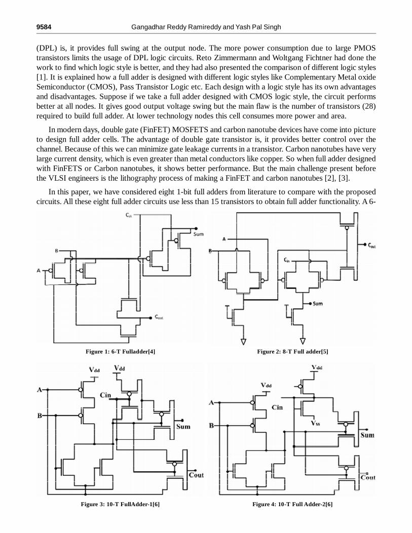
In this paper, we have considered eight 1-bit full adders from literature to compare with the proposedcircuits. All these eight full adder circuits use less than 15 transistors to obtain full adder functionality. A 6-
Figure 1: 6-T Fulladder[4] Figure 2: 8-T Full adder[5]
Figure 3: 10-T FullAdder-1[6] Figure 4: 10-T Full Adder-2[6]

Design of Robust, Ultra Low-Power Efficient Full Adder Cell in sub-45nm Technologies 9585
transistor full adder was designed with the aid of two novel transistor XOR Gates [4]. The 6-transistor isshown in Fig. 1. Fig. 2 shows an 8-transistor full adder [5]. From [6], two 10-transistor circuits are takenand these two 10-transistor full adders are shown in Fig. 3 and Fig. 4.
R. Shalem et al. proposed a low count 10 transistor full adder, named Static Energy Recovery Fulladder (SERF) [7]. SERF adder is shown in Fig. 5. Latter a new full-adder circuit using double gate FinFETtransistor and Gate Diffusion Input (GDI) technique [8]. Fig. 6 depicts a 10 Transistor full adder designedwith GDI technique. In [6], authors proposed 14-Transistor full-adder-1 and is depicted in Fig. 7. Fig. 8represents 14T full adder-2 [9]. This full adder cell uses novel XOR, XNOR gates and transmission gatesto generate the sum and carry out with 14 transistors half of the PMOS and another half NMOS.
3. PROPOSED METHOD
The full adder functionality can be represented in many ways so far in literature. The logic function for thenewly proposed full-adder is represented as
( ) ( )in inSum C A B C A B� � � � (1)
Figure 5: Static Energy-RecoveryFA[7] Figure 6: 10-T GDI Logic FA[8]
Figure 7: 14 TFA-1[6] Figure 8: 14 T FA-2[9]

9586 Gangadhar Reddy Ramireddy and Yash Pal Singh
( ) ( )inCarry A B C A B A� � � � (2)
Eq. (1) can be implemented with two Low Power (LP) XOR/XNOR gates which are proposed in [10].Eq. (2) can be implemented with a 2 to 1 multiplexer, implemented with two transistors one is NMOS andanother is PMOS, this is possible of complementary control signal which are intermediate signals XOR/XNOR.
Based on the logic expressions in Eq. 1 & 2, the 1-bit full adder can be implemented with only 10transistors. The proposed 10 transistor full adder is depicted in Fig. 9. This circuit requires only non-complementary inputs. A and B input signal are applied to the first XOR gate. The output of the first XORgate is A ��B. This signal is applied to the second XOR gate along with Carry input signal. The output ofthe second XOR gate is A ��B ��C
in. So, sum signal is obtained at the output node of second XOR gate.
Now, we will analyze the operation for carry out signal. By analyzing the truth table of 1-bitfull adder, thefollowing conclusions can be drawn.
• When the A ��B signal is high, carry out signal follows the carry in signal.
• When A ��B signal is low, carry out signal follows input A or B signal.
By using this property, a multiplexer is used to implement it. A ��B Signal is given as a control signalto the multiplexer. Single NMOSFET and single PMOSFET are used to form a multiplexer gate. For thismultiplexer one input is carry in signal and it is applied to NMOSFET, another is A signal and it is appliedto PMOSFET. The output of the multiplexer is carry out signal.
So, only 10 transistors are required to construct the novel full adder circuit. The problem with theproposed 10 transistor full adder cell is that at the output node, full rail to rail logic levels are not appearing.This is because of the two transistor multiplexer, is providing output voltages with the loss of Vth. So, toget the complete voltage swing at output node, transmission gate logic is used. In this way, the loss ofthreshold voltage at output can be eliminated. The designed full adder is named as the proposed novel 14Tfull adder and it is depicted in Figure 10. The authors in [11] have done a comparison of different types ofXOR/XNOR gate in literature with the Low Power (LP) XOR/XNOR gates in terms of leakage power.
Figure 9: Proposed novel 10T Full adder

Design of Robust, Ultra Low-Power Efficient Full Adder Cell in sub-45nm Technologies 9587
This study has shown that the leakage power of LP XOR/XNOR gate is the lowest. Leakage power is thedominating factor in power consumption at sub-micron technologies. So, in this work LP XOR/XNORgates are used to design the full adder circuits.
4. SIMULATION RESULTS
All designed circuits in this paper are simulated using Spectre simulator in Virtuoso Design Environmentprovided by Cadence Software. Designed circuits are captured using Generic Process Design Kit (GPDK)and 45nm technology transistor models are used. Simulations are done under GPDK45nm technology fileprovided by the Cadence Design Systems. The input combinations are taken from 000 to 111 and thesimulation time is 20ns.
Furthermore, Table 1 gives the information of different types of full adders presented in this paper andalso shows with which logic style each full adder is designed. Most of the full adders in this work considered
Figure 10: Modified novel 10T Full Adder (Proposed novel Full Adder 14T Full Adder)
Table 1Features of Full adder designs under comparison
Full-Adder # of Transistors Circuit Type Voltage Swing
6-T FA 6 PTL Degraded
8-T FA 8 PTL Degraded
10-T FA-I 10 PTL Degraded
10-T FA-II 10 PTL Degraded
GDI 10-T FA 10 GDI Logic Degraded
14-T FA-I 14 PTL+TG Full
14-T FA-II 14 PTL Full
SERF 10 PTL Degraded
Proposed 10-T FA 10 PTL Degraded
Proposed 14-T FA 14 PTL+TG Full
PTL - Pass Transistor Logic, TG - Transmission Gate Logic, GDI- Gate Diffusion Input

9588 Gangadhar Reddy Ramireddy and Yash Pal Singh
are which are designed with pass transistor logic. Based on the simulation results and waveforms obtained,it can be mentioned that the 6-T, 8-T, 10-T FA-I, 10-T FA-II, full adder designed with GDI logic, and self-energy recovery full adder circuits give degraded carry out and sum signals at output. 14-T FA-I and 14-TFA-II along with, the two proposed full adders with low power XOR gate and pass transistors give fullswing at output node. In the proposed full adder, if we observer the carry out structure, the carry out signalis coming from the output of a pass transistor. NMOS FET has week one characteristic and PMOS FET hasweek zero characteristic, so the output is a degraded signal.
Table 2 presents the simulation results of all 1-bit full adders considered in this work. From Table 2 itcan be analyzed that the proposed 10 Transistor full adder gives better power delay product figure than thatgiven by other full adder circuits. Next to proposed 10 transistor full adder proposed 14 transistor full addergives better performance. Transistor count of the adders is checked in order to investigate their impact onpower dissipation of a circuit. Even though a circuit is designed with less number of transistors, the outputmay be degraded This can be observed for the case of 6T 1-bit full adder cell.
Supply voltage variations cause delay uncertainty. It is very important issue in high performance VLSIcircuits and some system design use multi supply voltages (voltage islands) in order to minimize the power.So, it is an essential task to verify the circuit behavior at lower supply voltages. Average power and delayvalues of proposed 14 transistor and 10 transistor full adders at different supply voltages are tabulated inTable 3 and Table 4 respectively.
Temperature fluctuations varies with the threshold voltage, carrier mobility, and saturation velocity ofa MOSFET. Operating an integrated circuit at the prescribed nominal supply voltage is not preferable for
Table 2Simulation results of various full-adders
Full Adder Average Power(nW) Delay(pS) PDP(×10–17 J )
6-T FA 1000 18 1.8
8-T FA 1500 58 8.7
10-T FA-I 104 144 1.4976
10-T FA-II 113.9 191 2.175
GDI 10-T FA 113 125 1.4125
14-T FA-I 156.5 20 3.12
14-T FA-II 146 149 2.175
SERF 70 50 0.35
Proposed 10-T FA 85 20 0.17
Proposed 14-T FA 118 23 0.27
Table 3Simulation result of proposed 14-T Full adder at Various Supply Voltages (V
dd)
Vdd(V) Average Power(nW) Delay(pS) PDP(×10–17 J )
1.4 205.1 14 0.287
1.3 187.1 17 0.3179
1.2 139.1 20 0.2782
1.1 118 23 0.27
1 101 24 0.2424
0.9 87.74 32 0.2808
0.8 81.82 40 0.32728
0.7 119.1 48 0.57168

Design of Robust, Ultra Low-Power Efficient Full Adder Cell in sub-45nm Technologies 9589
reliable circuit operation under temperature variations. Propagation delay of a circuit is a function of thedrain saturation current produced by active transistors. So the designed full adder cell is simulated atdifferent temperatures, propagation delay and average power is noted. Table 5 gives the information ofaverage power and delay of the proposed 10T full adder at cell at temperature range from -200c to+80 0c.
The proposed full adder simulation waveforms have shown in Fig. 12 and 13. By observing the simulationwaveforms, it can be said that, 6, 8, two 10 transistor full adders, GDI logic based full adder, two 14
Table 4Simulation result of Proposed 10-T Full adder at Various Supply Voltages (Vdd)
Vdd
(V) Average Power(nW) Delay(pS) PDP(×10–17 J )
1.4 379 38 0.14402
1.3 308.3 57 1.7573
1.2 243.7 94 2.2907
1.1 86 22 0.1892
1 149 336 05.0064
0.9 115 900 1.035
0.8 80.31 1000 0.32728
Table 5Average Power and Delay of Proposed 10T Full Adder at different Temperatures
Temperature(oC) Average Power(nW) Delay(ps)
-20 180.5 200
-10 182.9 191
0 185.5 184
10 187.8 178
20 190.2 173
30 192 170
40 195.2 166
50 198.5 164
60 200 163
70 203 161
80 206 161
Figure 11: Waveform of test pattern

9590 Gangadhar Reddy Ramireddy and Yash Pal Singh
Figure 13: Simulation waveform of proposed 14T full adder
Figure 12: Simulation waveform of proposed 10T full adder
transistor full adders and static energy recovery full adder circuits are not producing the correct functionalityof the full adder logic for the given input signals. The proposed full adder circuits working properly for theinput combinations (ABCin) from 000 to 111. The input pattern is given in Fig. 11
5. CONCLUSION
In this paper, a novel 10 transistor full adder is proposed and is modified to give the better logic levels at theoutput node. Parametric analysis of 14T and 10T full adder shows that the proposed circuit works at 45nmtechnology node effectively well. From Table I, it is showed that the proposed novel full adder consumesless power and worst case delay is also less compared to existing full adder cells. Based on the observationof simulated output waveforms, it can be said that the proposed full-adder circuit has better output voltageswings than that of 10T and 10T GDI full-adder circuits existed in the literature.
REFERENCES[1] R. Zimmermann and W. Fichtner, “Low-power logic styles: CMOS versus pass-transistor logic,” IEEE Journal of Solid-
State Circuits, vol. 32, no. 7, pp. 1079–1090, 1997.
Design of Robust, Ultra Low-Power Efficient Full Adder Cell in sub-45nm Technologies 9591
[2] I. Hassoune, X. Yang, I. O’Connor, and D. Navarro, “Ultra-low power full adder circuit using SOI double-gatemosfetdevices,”Electronics Letters, vol. 44, no. 18, pp. 1095–1096, 2008.
[3] J. Liu, I .O’Connor, D. Navarro, and F. Gaffiot, “Design of CNTFET-based reconfigurable logicgate,” Electronics Letters,vol. 43, no. 9, pp. 514–516, 2007.
[4] C. Pakkiraiah, S. Adilakshmi, and K. Neelima, “Design of high speed six transistor full adder using a novel two transistorXOR gates,” International Journal of Advanced Research in Computer Science and Electronics Engineering, vol. 1, no.5, pp. 345–348, 2012.
[5] S. R. Chowdhury, A. Banerjee, A. Roy, and H. Saha, “A high speed 8 transistor full adder design using novel 3transistorxorgates,” International Journal of Electrical, Computer, Energetic, Electronic and Communication Engineering,vol. 2, no. 10, pp. 2244–2250, 2008.
[6] C.H. Chang, J. Gu, and M. Zhang, “A review of 0:18nm full adder performances for tree structured arithmeticcircuits,”Journal of Transactions on VLSI Systems, vol. 13, no. 6, pp. 686–694, 2005.
[7] R. Shalem, E. John, and L. K. A. John, “A novel low power energy recovery full adder cell,” Ninth Great Lakes Symposium,vol.-, no.-, pp. 380–383,1999.
[8] S. Abbasalizadeh and B. Forouzandeh, “Full adder design with gdi cell and independent double gate transis tor,”IranianConferenceon Electrical Engineering, vol. 2, pp. 130–134, 2012.
[9] E. Abu-AShama and M. Bayoumi, “A new cell for low power adders,” International Symposium on Circuits and Systems,vol. 4, pp. 49–52,1996.
[10] J. M. Wang, S. C. Fang, and W. S. Feng, “New efficient designs for XOR and nor functions on the transistor level,”IEEEJ. Solid-State Circuits, vol. 29, no. 7, pp. 80–86, 1994.
[11] G. Merrett and B. M. Al-Hashimi, “Leakage power analysis and comparison of deep submicron logic gates,” IntegratedCircuit and System Design, Power and Timing Modeling, Optimization and Simulation, vol. 3254, pp. 198–207, 2004.
Related Documents