I (Design of Multiband Patch antenna using Fractal design and Defected Ground Structured for Wireless Applications) A Thesis Submitted in partial fulfillment of the requirements for the award of the degree of DOCTOR OF PHILOSOPHY in (Electronics and Electrical Engineering) By Amandeep Kaur (41400724) Supervised By Prof. Dr. Praveen Kumar Malik Lovely Professional University Punjab 2020

Welcome message from author
This document is posted to help you gain knowledge. Please leave a comment to let me know what you think about it! Share it to your friends and learn new things together.
Transcript

I
(Design of Multiband Patch antenna using Fractal design and
Defected Ground Structured for Wireless Applications)
A Thesis
Submitted in partial fulfillment of the requirements for the
award of the degree of
DOCTOR OF PHILOSOPHY
in
(Electronics and Electrical Engineering) By
Amandeep Kaur
(41400724)
Supervised By
Prof. Dr. Praveen Kumar Malik
Lovely Professional University
Punjab 2020

II
DECLARATION
I hereby declare that this research work “Design of Multiband Patch antenna using Fractal
design and Defected Ground Structured for Wireless Applications” has been composed
solely by myself and has not been submitted anywhere. It was carried out by me for the
degree of Doctor of Philosophy in Electrical Engineering under the guidance and
supervision of Prof. Dr. Praveen Kumar Malik, Lovely Professional University, Phagwara
Punjab, India.
The interpretations put forth are based on my reading and understanding of the original
texts and they are not published anywhere in the form of books, monographs or articles.
The other books, articles and websites, which I have made use of are acknowledged at the
respective place in the text.
I certify that
• The work contained in this thesis is original and has been done by me under the
guidance of my supervisor (s).
• The work has not been submitted to any other Institute for the reward of any other
degree or diploma.
• I have followed the guidelines provided by the Institute in preparing the thesis.
• Whenever I used materials (data, theoretical analysis, figures and text) from other
sources, I have given due credit to them by citing them in the text of the thesis and
giving their details in the references.
Date: 21/10/2020
Amandeep Kaur
(41400724)

III
CERTIFICATE
This is to certify that the thesis entitled “Design of Multiband Patch antenna using
Fractal design and Defected Ground Structured for Wireless Applications” being
submitted by Amandeep Kaur for the degree of Doctor of Philosophy in Engineering from
Lovely Professional University, Jalandhar is a record of bonafide research work carried out
by her under my supervision at the School of Electrical and Electronics Engineering. In
our opinion, this is an authentic piece of work for submission for the degree of Doctor of
Philosophy. To the best of our knowledge, the work has not been submitted to any other
University or Institute for the award of any degree or diploma.
Supervisor
Dr. Praveen Kumar Malik, Professor
School of Electrical and Electronics Engineering
Lovely Professional University, Phagwara, Punjab-144011
E-mail id: [email protected]
Phone No: +91-9719437711
IV
ABSTRACT
With the tremendous growth of wireless communication application, set the way on new
design specification for integrated devices which demands more compactness, low profile
and cheap in cost. In wireless signal transmission, antenna plays significant role to convert
electrical signals into electromagnetic waves and act as transducer at transmitter and
receiver side. To reduce overall circuit dimensions for RF components, antenna
miniaturisation is becoming essential to obtain optimized design for handheld wireless
communication gadgets and to accomplish this PCB technology based micro-strip patch
antenna becomes buzz word which gain researches attention for more compact size with
good gain and bandwidth characteristics. Moreover, wireless devices like Mobile phones
operates on different technologies like ISM band for Wi-Fi, Bluetooth BLE and Wi-MAX,
GSM, CDMA etc. Conventional antenna mainly operates on single band of frequency but
now there is need to design multiple band antenna which can resonates on different
frequency band and omit the need of multiple antenna in one device. To achieve high data
transmission rates, antenna must full-fill the minimum band requirements set by FCC for
every wireless standard.
So, Microstrip patch antenna is highly regarded and it is the proved as the best candidate
for Wireless communication applications due to several characteristics which meets the
wireless communication devices requirements like light in weight, low profile, easy
integration with microwave circuits and cheap in cost as fabricated using PCB technology
but has some down side like less gain and bandwidth. In literature, researchers use
numerous methods for micro-strip patch antenna gain, bandwidth enhancement with more
compactness and multi band characteristics. In micro-strip patch antenna, multiple band
characteristics can be achieved by modification to the patch structure which act as main
radiator using two strategies mainly. The first one is by designing different patches for
different frequencies or second approach is by increasing electrical length of patch without
increasing overall antenna dimensions to achieve multi band behaviour. Second method is
mainly adopted and can be accomplished using Fractal and defected ground structures.
V
The use of fractal structures in antenna designing has significantly impacted its use for
various communication technologies. Fractal shapes are known for their space filling and
self-similarity properties. Due to these characteristics, antenna minimization can be
achieved by electrically increasing the length of current transmission in patch which acts
as main radiator without physically changing antenna structure. Self-similarity property
means, same geometry is repeated several times but with small dimensions of previous
one, which leads to obtain multiple resonance to gets multi band behaviour. Further, to
improve micro-strip patch antenna small gain, narrow impedance bandwidth and to supress
cross-polarization defected ground structures are used due to it simple design. Etched slots
or defects in the ground plane or micro-strip patch antenna are called defected ground
structure and there can be single or multiples defects.
Main purpose of this thesis is to design multi band microstrip patch antenna with wide
bandwidth using fractal and defected ground structures for wireless applications. Circular
cut fractal antenna with U-shaped defected geometry with truncated edges and Elliptical
shaped with steps cut fractal defected antenna have been proposed. The Antenna are
simulated using HFSS simulator and fabricated using PCB fabrication technology.
Antenna performance is analyzed in terms of return loss, gain, impedance bandwidth and
radiation pattern. Proposed antenna shows multi band characteristics for wireless
applications.
Circular cut fractal antenna with U-shaped defect is compact in size with dimensions 42mm
x 52mm, which is fabricated on Rogers RT Duroid 5880 dielectric substrate with thickness
1.6mm and dielectric constant (ε) 2.2. Antenna resonates on frequencies 3.80, 7.01, 10.86,
11.84GHz with bandwidth 260, 330, 270 and 460MHz respectively. For proposed antenna,
maximum gain achieved at these resonating frequencies are 5.52, 8.05, 5.32 and 7.78dB
respectively. Antenna is simulated and fabricated results are agreement with each other.
An elliptical patch shaped fractal antenna is also simulated and fabricated on Rogers RT
Duroid 5880 material with thickness 0.8mm. Antenna overall dimensions are 50 mm x
50mm x 0.8mm. Antenna shows multi band behavior and resonates on three frequency
band 2.6, 6 and 8.2GHz with impedance bandwidth of 410, 1070, and 4840MHz
VI
respectively with maximum gain achieved of 5.52dB. Simulated and measured results
shows that proposed antenna is used good candidate for wireless communication
applications and covers different wireless standards like Wi-Fi (2.4GHz), Bluetooth
version V1.0-V4.0, WLAN (2.4/5.2/5.8GHz), WiMAX (2.3/2.5/5.5GHz), Wireless Body
Area Network (2.3/2.4GHz), RFID (2.4 to 2.5/5.85 to 5.925GHz), Microwave ovens (2.4
to 2.48GHz) which falls under ISM (Industrial Scientific and Medical) band applications.
It also covers RADAR (2.33 to 2.74/5.4), Geostationary Satellite communication (11.7 to
12.2GHz), X-band application (8 to 12GHz), S-Band (2.3 to 2.4GHz) communication,
Wireless Communication Services (WCS) 2.345 to 2.360GHz, and 4GLTE (2.3 to
2.315GHz) wireless communication standards. Proposed antenna shows multi band
characteristics with wideband characteristics for wireless applications.

VII
ACKNOWLEDGEMENT
Throughout the writing of this dissertation I have received a great deal of support and
assistance.
First and foremost, I would like to express my deep and sincere regards for my supervisor,
Prof. Dr. Praveen Kumar Malik for providing me the opportunity, support and freedom to
carry on this research work. His passion, guidance, and discipline have been indispensable
to my growth as a scientist and as a person over these past four years. I am especially
grateful for his devotion to his students’ education and success.
I wish to acknowledge the infrastructure and facilities provided by School of Electrical and
Electronics Engineering, Lovely Professional University and Research department to guide
me on timely basis regarding norms and guidelines.
I would like to pay my special regards to Mr Rajesh Khanna and Mr. Hitender for his
technical support in the Electronics Department of Thapar University Patiala, Punjab.
Last, but not the least I would express my sincere gratitude to my family for their love,
sacrifice and moral support for without their continued support this work would never have
been possible.
VIII
CONTENTS
Declaration II
Certificate III
Abstract IV
Acknowledgements VII
Contents VIII
List of Figures XII
List of Tables XVI
Acronyms and Abbreviations XVII
List of Symbols XXII
Table of Contents
CHAPTER-1 ................................................................................................................................... 1
INTRODUCTION.......................................................................................................................... 1
1.1 INTRODUCTION .......................................................................................................... 1
1.2. WIRELESS STANDARDS ................................................................................................ 3
1.2.1 GSM ................................................................................................................................ 3
1.2.3 IEEE standard for WLAN ............................................................................................... 3
1.2.4 IEEE standard for WiMAX............................................................................................. 4
1.2.5. IEEE standard for BLUETOOTH .................................................................................. 4
1.2.6. LTE (Long Term Evolution) .......................................................................................... 5
1.2.7. 5G (Fifth Generation) .................................................................................................... 5
1.2.8. LoRa (Long Range Radio)- IEEE 802.15.4g ................................................................ 5
1.2.9. WBAN (Wireless Body Area Networks) IEEE 802.15.69 ............................................ 7
1.3. MOTIVATION ................................................................................................................... 7
1.4. STATEMENT OF PROBLEM .......................................................................................... 9
1.5. SCOPE OF PRESENT WORK ....................................................................................... 10
1.6. THESIS OUTLINE ........................................................................................................... 10
1.7. SUMMARY ....................................................................................................................... 12
ANTENNA OVERVIEW ............................................................................................................ 13
2.1. INTRODUCTION............................................................................................................. 13

IX
2.2. ANTENNA PARAMETERS ............................................................................................ 13
2.3. INTRODUCTION TO MICRO-STRIP PATCH ANTENNA ...................................... 19
2.4. MICRO-STRIP ANTENNA FEEDING TECHNIQUES .............................................. 21
2.5. MICROSTRIP PATCH ANTENNA ANALYSIS METHODS .................................... 25
2.6. SUMMARY ....................................................................................................................... 30
CHAPTER-3 ................................................................................................................................. 31
STATE OF ART .......................................................................................................................... 31
3.1. INTRODUCTION............................................................................................................. 31
3.2. LITERATURE REVIEW ................................................................................................ 31
3.3. SUMMARY ....................................................................................................................... 57
RESEARCH METHODOLOGY FOR THE RESEARCH WORK ....................................... 58
4.1 INTRODUCTION.............................................................................................................. 58
4.2.1 HFSS (High Frequency Structure Simulator) ............................................................... 58
4.2.2 Vector Network Analyzer ............................................................................................. 62
4.2.3. Spectrum Analyzer ....................................................................................................... 65
4.3 SUMMARY ........................................................................................................................ 67
CHAPTER-5 ................................................................................................................................. 69
CONFIGURATION OF ANTENNA DESIGN ......................................................................... 69
5.1 INTRODUCTION.............................................................................................................. 69
5.2 FRACTAL STRUCTURES .............................................................................................. 69
5.2.1 Classification of Fractal Structures ............................................................................... 71
5.2.3 Commonly used Fractal Geometries for Antenna designing ........................................ 72
5.2.4 Fractals features ............................................................................................................ 76
5.2.5 Fractals Advantages and Disadvantages ....................................................................... 77
5.3 DEFECTED STRUCTURES ............................................................................................ 78
5.3.1 Evolution of DGS ......................................................................................................... 79
5.3.2 Working principle of DGS ............................................................................................ 79
5.4 MULTI BAND CIRCULAR CUT, U-SHAPED DEFECTED GROUND
MICROSTRIP PATCH ANTENNA ...................................................................................... 81
5.5 ANTENNA SIMULATED RESULTS ............................................................................. 86
5.6 ANTENNA FABRICATION .......................................................................................... 103

X
5.7 SUMMARY ...................................................................................................................... 106
CHAPTER-6 ............................................................................................................................... 108
ELLIPTICAL PATCH MULTI BAND ANTENNA USING FRACTAL AND DEFECTED
GROUND STRUCTURES ........................................................................................................ 108
6.1. INTRODUCTION........................................................................................................... 108
6.2 ANTENNA DESIGN ....................................................................................................... 108
6.3 ANTENNA MATEHMATICAL MODELLING .......................................................... 111
6.5 ANTENNA FABRICATION .......................................................................................... 123
6.5.1 Antenna Gain and Radiation Pattern Measurements .................................................. 127
6.6 PARAMETRIC ANALYSIS ........................................................................................... 130
6.6.1 Effect of substrate material ......................................................................................... 130
6.6.2 Effect of substrate thickness ....................................................................................... 131
6.6.3 Effect of Iterations ...................................................................................................... 132
6.7 COMPARATIVE ANALYSIS ........................................................................................ 133
6.8 SUMMARY ...................................................................................................................... 136
CHAPTER-7 ............................................................................................................................... 137
CONCLUSION AND FUTURE SCOPE ................................................................................. 137
APPENDIX A ............................................................................................................................. 141
A.1 ANTENNA FABRICATION ......................................................................................... 141
A.2 ANTENNA TEST PROCEDURE ................................................................................. 143
A.2.1 Return loss/VSWR measurement using VNA (8720A) ............................................. 144
` ` A.2.2 Antenna Gain measurement ............................................................................. 146
A.2.3 RADIATION PATTERN MEASUREMENT ........................................................... 149
Bibliography ............................................................................................................................... 150
XI
List of Figures
Figure 1.1 Wireless communication networks.....................................................................2
Figure 1.2 Different shapes of patch used for Microstrip patch antenna .............................3 Figure 2.1 VSWR measurement along Transmission line .................................................17
Figure 2.2 Antenna radiation pattern .................................................................................18
Figure 2.3 A Typical Microstrip Patch Antenna ................................................................20
Figure 2.4 Applications of Microstrip Patch antenna in different fields ...........................21
Figure 2.5 Geometry of Microstrip line fee patch antenna [35] ........................................22
Figure 2.6 Geometry of Coaxial Probe Feed patch antenna [35] .....................................23
Figure 2.7 Geometry of Aperture Coupled Microstrip Patch Antenna [35] ......................24
Figure 2.8 Geometry of Proximity Coupled Microstrip Patch Antenna [35] ....................24
Figure 2.9 Microstrip patch antenna Analysis methods classification .............................27 Figure 4.1 Ansys HFSS simulation procedure for Antenna designing ..............................59
Figure 4.2 Practical two port Vector Network Analyzer ...................................................62
Figure 4.3 Setup for S-Parameter Measurement of DUT ..................................................63
Figure 4.4 S11 co-efficient representation for 2-port network ..........................................64
Figure 4.5 Block diagram of Filter Bank Spectrum Analyzer ...........................................66
Figure 4.6 Block diagram of Super heterodyne Spectrum analyzer ..................................67
Figure 5.1General Antenna design procedure ...................................................................70
Figure 5.2 Fractal geometries available in Nature [120] ...................................................71
Figure 5.3 Classification of Fractal Structures on basis of Deterministic and Non-
Deterministic Behaviour ....................................................................................................72
Figure 5.4 Sierpinski Gasket Fractal Geometry [120] .......................................................73
Figure 5.5 Sierpinski Carpet Fractal Structure [123] .........................................................73
Figure 5.6 Koch curves Fractal structure [123] .................................................................74
Figure 5.7 Minkowski curves Fractal structure [123] ........................................................75
XII
Figure 5.8 Cantor Set fractal geometry [123] ....................................................................75
Figure 5.9 Hilbert curve Fractal Structures [123] ..............................................................76
Figure 5.10 Different DGSs shapes reported in lecture [130] ...........................................79
Figure 5.11 The first DGS unit: (a) dumbbell DGS unit; (b) S parameter performance
[133]. ..................................................................................................................................80
Figure 5.12 (a) Basic design (b) Iteration-1: Top view (c) Iteration-2: Top view .............83
Figure 5.13 (a) Iteration-1: VSWR vs frequency plot (b) Iteration-1: Return loss vs
frequency plot ....................................................................................................................87
Figure 5.14 Gain of proposed antenna at different frequencies for phi and theta value.89
Figure 5.15 (a) Iteration-2: Return loss (S11) v/s frequency response(b)Iteration-2: VSWR
vs Frequency plot ...............................................................................................................90
Figure 5.16 Iteration-2 gain at different frequencies .........................................................92
Figure 5.17 (a) S11 v/s Frequency performance for Iteration-3 (b) VSWR vs Frequency
plot of Iteration-3 ...............................................................................................................93
Figure 5.18 Gain at different frequency with phi and theta values for Iteration-3 ............93
Figure 5.19(a) Return loss v/s Frequency response of Iteration-4 (b) VSWR vs Frequency
plot of Iteration -4……………………………………………………………………………………. 98
Figure 5.20 Gain at different frequencies with Phi and theta of Antenna-4 ......................95
Figure 5.21 S11 v/s frequency performance of Iteration-5 ................................................97
Figure 5.22 VSWR v/s frequency performance of Iteration-5 ..........................................97
Figure 5.23 Gain at different frequencies with Phi and theta for Iteration-5 .....................98
Figure 5.24 Radiation pattern for Phi=0 and 90 degree (a) At 3.80GHz (b) At 7.01GHz (c)
At 10.86GHz and (d) At 11.84GHz .................................................................................101
Figure 5.25 3-D Polar Plot at different frequencies (a) At 3.80GHz (b) At 7.01GHz (c) At
10.86GHz and (d) At 11.84GHz ......................................................................................103
Figure 5.26 Proposed Fabricated Antenna (a) Top view (b) Back view .......................104
Figure 5.27 Proposed antenna Return loss and VSWR measurement Setup ...................104
Figure 5.28 Simulated and Measure Return loss performance ........................................105
Figure 5.29 Measured VSWR performance for proposed antenna ..................................106
XIII
Figure 6.1Multi band Elliptical Shaped Fractal and Defected Antenna (a) Iteration-1
(n=1) (b) Iteration-2 (n=2) (c) Iteration-3 (n=3) (d) Defected Ground (Back view) .......115
Figure 6.2 Proposed Antenna top dimensions (a) and defected ground: Back with
expanded view (b,c) .........................................................................................................116
Figure 6.3 Proposed Antenna E-field distribution ...........................................................117
Figure 6.4 Simulated Return loss performance for multi band Elliptical patch antenna .119
Figure 6.5 Simulated VSWR performance for multi band Elliptical patch antenna .......120
Figure 6.6 Simulated Gain performance for multi band Elliptical patch antenna ...........120
Figure 6.7 Simulated 3-D Polar gain plot for proposed Elliptical patch Multi band band
fractal and defected antenna .............................................................................................121
Figure 6.8 Radiation pattern at 2.6GHz, 6GHz and 8.2GHz for (a) phi=0-degree (b)
Phi=90 degree ..................................................................................................................122
Figure 6.9 Proposed Fabricated Antenna (a) Top view (b) Back view (c) SMA connector
used ..................................................................................................................................124
Figure 6.10 Proposed antenna Return loss Measurement Setup ......................................124
Figure 6.11 Simulated and Measured Return loss plot for proposed antenna .................125
Figure 6.12 Measured Return loss extended plot for proposed antenna ..........................125
Figure 6.13 Simulated and Measured VSWR performance for proposed antenna ..........126
Figure 6.14 Simulated and Measured Gain for proposed elliptical shaped patch multi
band antenna ....................................................................................................................127
Figure 6.15 Measured and Simulated radiation pattern at 2.6GHz in H-plane
(Phi=90degree) for proposed antenna ..............................................................................128
Figure 6.16 Measured and Simulated radiation pattern at 6GHz in H-plane
(Phi=90degree) for proposed antenna ..............................................................................129
Figure 6.17 Measured and Simulated radiation pattern at 8.2GHz in H-plane
(Phi=90degree) for proposed antenna ..............................................................................129
Figure 6.18 Proposed antenna S11 performance with Rogers and FR4(t=0.8mm) .........131
Figure 6.19 Proposed antenna S11 performance with different substrate height ............132
Figure 6.20 Effect of different Iterations on S11 performance .......................................133
XIV
Figure A.1 PCB Fabrication process ...............................................................................142
Figure A.2 VNA Equipment used for proposed antenna Return loss and VSWR
measurement ....................................................................................................................144
Figure A.3 Test setup for VSWR measurement ..............................................................145
Figure A.4 Test setup for Insertion Loss measurement ...................................................147
Figure A.5 Test setup for Gain measurement ..................................................................148

XV
List of Tables
Table 1. 1 Different Wireless standards used with frequency of operation and bandwidth 6 Table 2. 1 Advantages and disadvantages of Microstrip patch antenna feeding methods 25 Table 5. 1 Structural Parameters of Proposed Antenna design ..........................................84
Table 5. 2 Bandwidth achieved with return loss for Iteration -1 ......................................88
Table 5. 3 Frequency bands and Gain achieved for Antenna-1 .........................................88
Table 5. 4 Bandwidth achieved with return loss for Iteration-2 ........................................90
Table 5. 5 Value of gain for different resonating frequency bands along with bandwidth
for Iteration-2 .....................................................................................................................91
Table 5. 6 Gain, S11 and bandwidth performance of Iteration-3 ......................................92
Table 5. 7 Gain, S11 and bandwidth performance of Iteration-4 .....................................95
Table 5. 8 S11, Gain and Bandwidth performance of Iteration-5 .....................................98
Table 5. 9 Return loss Simulated and Measure comparison of proposed antenna ..........106 Table 6. 1 Dimensions of Proposed Elliptical shaped patch multi band Fractal and
Defected Ground Antenna ...............................................................................................113
Table 6. 2 Proposed antenna Simulated results in terms of S11, Gain, VSWR and
Bandwidth ........................................................................................................................118
Table 6. 3 Proposed antenna performance comparative analysis with existing antenna .133 Table A. 1 Apparatus used for Antenna parameter measurement ..................................143
Table A. 2 Antenna testing devices used for Proposed antenna Measurement ...............143
XVI
Acronyms and Abbreviations
Acronyms Description
2-D Two Dimensional
2G 2nd Generation
3-D Three Dimensional
3GPP 3rd Generation Partnership Project
4G 4th generation
5G 5th generation
AF Audio Frequency
AMC Artificial Magnetic Conductor
AMPS Advanced Mobile Phone Service
AR Axial Ratio
ARBW Axial Ratio Bandwidth
AUT Antenna Under Test
BPF Band Pass Filter
BW Bandwidth
CP Circular Polarization
CPW Coplanar Waveguide
CRO Cathode-Ray Oscilloscope
CRT Cathode-Ray Tube
CSMA/CA Carrier Sense Multiple Access/ Collision Avoidance
CST Computer Simulation Technology

XVII
DGS Defected Ground Structures
DUT Device Under Test
EBG Electromagnetic Bandgap
EDGE Enhanced Data for Global Evolution
EDR Enhanced Data Rate
EIRP Equivalent Isotopically Radiated Power
ETSI European Telecommunications Standards Institute
FDGS Fractal Defected Ground Structure
FDTD Finite Difference Time Domain
FEM Finite Element Method
FFT Fast Fourier Transform
FHSS Frequency Hopping Spread Spectrum
FR4 Flame Retardant 4
FSA Fibonacci spiral antenna
FSPL Free Space Path loss
GNSS Global Navigation Satellite System
GPA Ground plane aperture
GPS Global Positioning System
GSM Global System for Mobile
GUI Graphical User Interface
HA Hybrid Antenna
HFSS High Frequency Structure Simulator
HIPERMAN High Performance Radio Metropolitan Area Network

XVIII
HORYU-IV High Voltage Technology Demonstration Satellite-4
HPBW Half Power Beam Width
IE3D Integral Equation Three-Dimensional
IEEE Institute of Electrical and Electronics Engineers
IFS Iterated Function System
IoT Internet of Things
ISM Industrial Scientific and Medical
LEO Low Earth Orbit
LHCP Left Hand Circular Polarized
LoRA Long Range
LPDA Log-Periodic Antenna
LPWAN Low-Power Wide-Area Network
LSNA Linear Sensor Node Array
LTE Long Term Evolution
M2M Machine 2 Machine
MAC Media Access Control
MIMO Multiple input Multiple Output
MM Metamaterial
MMOG Multi Media Online Gaming
MNM Multiport Network Model
MoM Method of Moments
MPA Microstrip Patch Antenna
MS Meta Surface
XIX
MTA Microwave Transition Analyzer
OFDM Orthogonal Frequency Division Multiplexing
PAN Personal Area Network
PBG Photonic Band Gap
PCB Printed Circuit Board
PHY Physical Layer
PIFA Planar Inverted F-Antenna
PMPA Planer Microstrip Patch Antenna
RADAR Radio Detection and Ranging
RCR Cherenkov radiation
RF Radio frequency
RFID Radio Frequency Identification
RHCP Right-Hand Circular Polarized
RL Return Loss
RSL Received Signal Level
SDT Spectral Domain Technique
SIG Special Interest Group
SMA Sub-Miniature version A
SNA Sliced Notch Antenna
SRR Split Ring Resonator
TCDA Tightly Coupled Dipole Array
TDMA Time Division Multiple Access
TEM Transverse Electric Magnetic

XX
TL Total Loss
TV Television
UHF Ultra-High Frequency
UMTS Universal Mobile Telecommunications System
VNA Vector Network Analyzer
VSWR Voltage Standing Wave Ratio
WBAN Wireless Body Area Networks
WCS Wireless Communication Services
Wi-Fi Wireless Fidelity
WiMAX Worldwide Interoperability for Microwave Access
WLAN Wireless Local Area Network
ZOR Zeroth-order Resonator

XXI
List of Symbols
Symbol Description
Η Efficiency
Γ reflection coefficient
𝜀𝑟 relative permittivity
tan δ loss tangent
λ Wavelength
c speed of light
fr resonating frequency
Z0 Characteristics Impedance
λg Guided Wave length
1
CHAPTER-1
INTRODUCTION
1.1 INTRODUCTION
From last few decades, with exponential growth in the wireless communication technology
and Internet services, the demand for high data rate services increased. Owing to this, the
number of users rose tremendously and can be widely seen that in the future
communication networks, huge traffic congestion will be experienced. To accomplish the
efficient communication services, good infrastructure is the big challenge for the
manufacturers and service providers to provide more capacity in the networks. Also,
compactness of devices is another big issue. There are some serious challenges faced in
wireless communication services like multipath fading, co-channel interference and delay
spread which degrade the signal quality [1]. Numerous methods are explored by researches
to maximize the efficiency of communication networks.
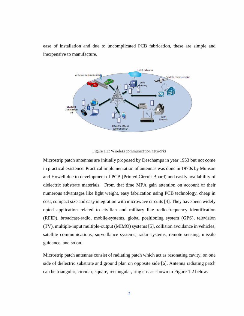
In the communication field, Wireless communication as shown in Figure 1.1 is the most
vibrant and fastest growing technology, in which information is transmitted from one end
to other end without making physical connections. Interestingly, in every communication
system, to transfer information transmitter and receiver play quintessential role and can be
deployed between few meters to thousands of kilometres like T.V remote and Satellite
communication respectively [2]. As, no guided medium is used, so transmission and
receptions of signals is achieved using Antennas.
Antenna is the device that converts electrical signal into radio waves on transmitter side
and vice versa on receiver side. Also, it is one of the crucial parts in circuit designing to
achieve compactness. Different types of antennas are available in the market like Horn
antenna, dipole antenna, PIFA, and microstrip patch antenna etc. [3]. Nowadays, in
communication systems low profile antennas are desired to achieve high performance over
wide range of frequencies. Due to such reasons microstrip patch antenna are gaining much
attention in this field and used widely because of their plentiful advantages like low in
profile, fair cost, planar structure, high robustness, and conformability to curved surfaces,
2
ease of installation and due to uncomplicated PCB fabrication, these are simple and
inexpensive to manufacture.
Figure 1.1: Wireless communication networks
Microstrip patch antennas are initially proposed by Deschamps in year 1953 but not come
in practical existence. Practical implementation of antennas was done in 1970s by Munson
and Howell due to development of PCB (Printed Circuit Board) and easily availability of
dielectric substrate materials. From that time MPA gain attention on account of their
numerous advantages like light weight, easy fabrication using PCB technology, cheap in
cost, compact size and easy integration with microwave circuits [4]. They have been widely
opted application related to civilian and military like radio-frequency identification
(RFID), broadcast-radio, mobile-systems, global positioning system (GPS), television
(TV), multiple-input multiple-output (MIMO) systems [5], collision avoidance in vehicles,
satellite communications, surveillance systems, radar systems, remote sensing, missile
guidance, and so on.
Microstrip patch antennas consist of radiating patch which act as resonating cavity, on one
side of dielectric substrate and ground plan on opposite side [6]. Antenna radiating patch
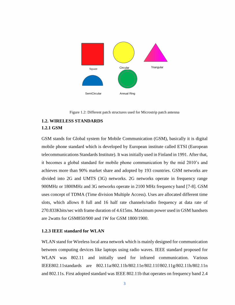
can be triangular, circular, square, rectangular, ring etc. as shown in Figure 1.2 below.
3
Figure 1.2: Different patch structures used for Microstrip patch antenna
1.2. WIRELESS STANDARDS
1.2.1 GSM
GSM stands for Global system for Mobile Communication (GSM), basically it is digital
mobile phone standard which is developed by European institute called ETSI (European
telecommunications Standards Institute). It was initially used in Finland in 1991. After that,
it becomes a global standard for mobile phone communication by the mid 2010’s and
achieves more than 90% market share and adopted by 193 countries. GSM networks are
divided into 2G and UMTS (3G) networks. 2G networks operate in frequency range
900MHz or 1800MHz and 3G networks operate in 2100 MHz frequency band [7-8]. GSM
uses concept of TDMA (Time division Multiple Access). Uses are allocated different time
slots, which allows 8 full and 16 half rate channels/radio frequency at data rate of
270.833Kbits/sec with frame duration of 4.615ms. Maximum power used in GSM handsets
are 2watts for GSM850/900 and 1W for GSM 1800/1900.
1.2.3 IEEE standard for WLAN
WLAN stand for Wireless local area network which is mainly designed for communication
between computing devices like laptops using radio waves. IEEE standard proposed for
WLAN was 802.11 and initially used for infrared communication. Various
IEEE802.11standards are 802.11a/802.11b/802.11e/802.11f/802.11g/802.11h/802.11n
and 802.11s. First adopted standard was IEEE 802.11b that operates on frequency band 2.4
Square Circular Triangular
SemiCircular Annual Ring
4
GHz ISM (Industrial and scientific) band with data rate of 11Mbps [9]. To achieve high
data rate transmission 802.11g designed that operates on 2.4GHz ISM band with data rate
up to 54Mbps. Afterwards second standard was defined which uses OFDM modulation
techniques and uses 5GHz ISM band. It gains more attention due to high transmission data
rate over small distances with suitable compatibility with devices and increased
development of antennas with large bandwidth.
1.2.4 IEEE standard for WiMAX
WiMAX is formed by WiMAX forum in June 200, mainly to promote and certify
interoperability and compatibility with others standards like IEEE 802.16and HIPERMAN.
WiMAX delivers broadband wireless services on the IEEE 802.16 set of standards, which
defines functions of the physical (PHY) and Media Access Control (MAC) layers. It works
like Wi-Fi but gives more data speed over larger distance and includes more users. It uses
two different models fixed 802.16d defined under 802.16a and often referred as 802.16-
2004 and mobile WiMAX IEEE 802.16e [10]. Fixed WiMAX used for fixed applications
like DSL with data rate upto 75Mbps. Mobile WiMAX, also called 802.16-2005, which
provides cheap services compared to Cellular Services with data rate up to 15Mbps within
cell radius of 2 to 4Km. It uses different frequency bands: 2.3GHz, 2.5GHz, 3.5GHz (3.4
to 3.69 GHz), and 5.5 GHz (5.25 to 5.85 GHz) as given in Table1.1.
1.2.5. IEEE standard for BLUETOOTH
Bluetooth technology is developed by Bluetooth Special Interest group (SIG) in 1998 under
IEEE standard 802.15.1. It is used in Personal Area Networks (PAN) to transfer data
between devices over small distances up to 30 feet using radio waves in Scientific and
Medical radio bands (SIM) i.e. 2.4GHz to 2.48GHz as shown in Table1.1. It has different
versions: First version 1.2 support data rate up to 1Mbps. Version 2 was 2.0+EDR with
data speed 0f 3Mbps following to third version 3.0+HS which has speed of 24Mbps.
Bluetooth technology uses Frequency Hopping Spread Spectrum (FHSS) multiple access
method to transfer data at 1600 hopes per second through 79 different channel each with
bandwidth of 1MHz.
5
1.2.6. LTE (Long Term Evolution)
LTE was started as a project by telecommunication body called the Third Generation
Partnership Project (3GPP) in 2004. It is based on the GSM/EDGE and UMTS
technologies which are used for mobile devices and data terminals to provide broadband
communication services. A tremendous growth in mobile data usage and development of
new applications like Mobile TV, Web 2.0, MMOG (Multimedia Online Gaming) and
streaming etc. motivated 3GPP to describe LTE to achieve more reliable networks in terms
of more capacity as well as speed and paved the way towards 4G mobile networks. First
version of LTE was documented in Release 8 of the 3GPP specifications. The LTE wireless
interface is not compatible with 2G and 3G networks, so it is operated on different radio
spectrum and different frequency bands are used in different countries which need multi
band mobile hence multi band antennas. Bands used are 700/1500/1700/2100/2600 MHz
with flexible bandwidths 1.4/3/5/10/15/20 MHz with downlink rates of 300Mbits/s and
uplink rate of 75Mbits/s [12].
1.2.7. 5G (Fifth Generation)
5G stands for 5th Generation, and this is the wireless technology for digital cellular mobile
networks which deployed in 2019. Frequency spectrum of 5G technology is divided into
three bands: millimeter waves, mid-band and low band. 5G millimeter is the fastest wave
with speed of 1 to 2 Gb/s and uses frequency bands above 24GHz to 72GHz. 5G mid-band
uses frequencies from 2.4Ghz to 4.2GHz [13-14]. This band is most widely used now, in
over 20 networks, offering speed between 100 to 400Mb/s over 100MHz band. China is
using 3.5GHz, while 3.3 and 4.2GHz bands are used by other countries. Low band works
similar to 4G and uses similar frequency range.
1.2.8. LoRa (Long Range Radio)- IEEE 802.15.4g
In wireless communication Bluetooth technology covers very less range for local
communication and consumes more power. The alternative technology used now in IoT
networks is LoRa. It is new technology, specifically designed for low power and long-
6
range wireless communication and developed by a company named Semtech. LoRa
stands for Long Range Radio and used for IoT and Machine-to-Machine (M2M)
networks. LoRa Alliance is the non-profit association that set standards for LPWAN
(Low Power Wide Area Networks) for IoT. This technology provides range of 2-5km
for Urban and 15Km for suburban area with data rates 0.3kbps to 50kbps and works on
spread spectrum modulation technique to avoid interference. LoRa technology operates
in ISM band 868MHz i.e. European ISM and 915MHz i.e. American ISM [15].
Table 1.1: Different Wireless standards used with frequency of operation and bandwidth
Wireless Standards Frequency Band of
operation (MHz)
Occupied bandwidth
(MHz)
GSM (Global System for
Mobile)
GSM-900: 890-960 70
GSM-1800: 1710-1805 95
GSM-1900: 1850-1990 140
WLAN (Wireless Local Area
Networks)
2400-2484 84
5150-5350 200
5725-5825 100
WiMAX (Worldwide
Interoperability for Microwave
Access)
2500-2690 190
3400-3690 290
5250-5850 600
Bluetooth 2400-2500 100
LTE (Long Term Evolution)
1710-1755 45
1710-1785 75
1850-1910 60
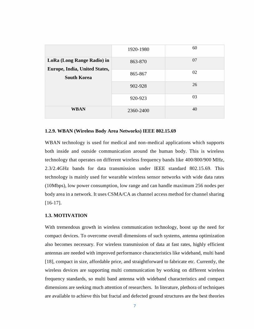
7
1920-1980 60
LoRa (Long Range Radio) in
Europe, India, United States,
South Korea
863-870 07
865-867 02
902-928 26
920-923 03
WBAN 2360-2400 40
1.2.9. WBAN (Wireless Body Area Networks) IEEE 802.15.69
WBAN technology is used for medical and non-medical applications which supports
both inside and outside communication around the human body. This is wireless
technology that operates on different wireless frequency bands like 400/800/900 MHz,
2.3/2.4GHz bands for data transmission under IEEE standard 802.15.69. This
technology is mainly used for wearable wireless sensor networks with wide data rates
(10Mbps), low power consumption, low range and can handle maximum 256 nodes per
body area in a network. It uses CSMA/CA as channel access method for channel sharing
[16-17].
1.3. MOTIVATION
With tremendous growth in wireless communication technology, boost up the need for
compact devices. To overcome overall dimensions of such systems, antenna optimization
also becomes necessary. For wireless transmission of data at fast rates, highly efficient
antennas are needed with improved performance characteristics like wideband, multi band
[18], compact in size, affordable price, and straightforward to fabricate etc. Currently, the
wireless devices are supporting multi communication by working on different wireless
frequency standards, so multi band antenna with wideband characteristics and compact
dimensions are seeking much attention of researchers. In literature, plethora of techniques
are available to achieve this but fractal and defected ground structures are the best theories
8
used to achieve such behaviour in microwave and antenna engineering field component
designing. Fractal geometries posse’s self-similarity and space-filling properties. Due to
self-similarity property of fractal structures, multiple resonances can be achieved in
antenna and it also increase the length of flow of electric current without increasing the
overall dimensions of device which leads to more compact structure. Defected ground
structures can any H, E, V, U shape defect in ground plane that increases antenna efficiency
in terms of gain and bandwidth. Wireless communication standards like Wi-Fi, Bluetooth,
Zigbee, GSM, GPS, LoRA, IoT, WiMAX, LTE/5G are most adopted standards for wireless
application in field of home automation, medical, industries etc. for wireless data sharing,
so, there is huge demand for multi-band antennas with good gain, wide impedance
bandwidth, small size and low profile single fed [19].
Microstrip patch antennas are generally considered as narrowband devices. Antenna
dimensions and performance highly depends on the frequency of operation and
wavelength. But this is still a serious issue in antenna designing to obtain compact designs
with respect to frequency. To deal with this problem, fractal and defected geometries can
be used and further can be extended to array designing to meet minimum requirements of
wireless communication systems. There are several reasons why fractal and defected
geometries gain much attention in antenna designing. First, multiple copies of same design
can be built up with different scaled values to design antenna with similar properties. [20-
21].
Second, due to their space filling property due to which antenna space can be utilized in
better way by using small scale fractal shapes [22-23]. Fractal antenna concept arises due
to mixture of two different disciplines, electromagnetism and geometry. Also, one more
technique that is seeking much attention now is Defected Ground Structures (DGS). Slots
and defects etched upon ground plane of microwave components are called Defected
Ground structures. It is opted method to enhance antenna parameters like operating
bandwidth, gain, cross-polarization etc. In literature, various defected structures have been
discovered and used like square, spiral, dumbbell, L-shaped, rectangular, circular, U-
shaped, hexagonal, V-shaped, concentric, arrow head etc. [24-29]. Current distribution and
9
propagation through ground plane can be controlled by properly selecting dimensions and
shapes of defected structures which further controls electromagnetic waves generation and
transmission through substrate material. Also, due to changes in inductive and capacitive
properties of ground plane, additional frequency bands can be achieved which leads to
multi band behaviour of circuits and very useful in wireless communication devices.
In this thesis, Multi band microstrip patch antennas are designed with fractal and defected
ground structures for wireless applications like Bluetooth, Zigbee, Wi-Fi, LoRa, GSM,
LTE etc. with frequency of operation from 1GHz to 15GHz. Two different antenna
prototypes are designed and tested based on fractal and defected geometry to obtain multi
band and wide bandwidth characteristic. First antenna is designed with circular cut
truncated edges patch with U-shaped defected ground on Roger RT Duroid 5880 material.
Four resonate frequency bands are achieved 3.93, 6.81, 10.79 and 11.64GHz with
bandwidth of 140, 280, 300 and 340MHz and gain of 5.52, 8.05, 5.32 and 7.87 dB
respectively. Second, elliptical shaped fractal patch with step cut defected ground antenna
is simulated and fabricated on Rogers RT Duroid 5880 dielectric substrate. Antenna
provides 3 resonant frequencies 2.6GHz, 6GHz and 8.2GHz with S11 co-efficient -18.18,
-15.11, -16.33dB and wide impedance bandwidth achieved are 410, 1070 and 4840MHz
with good gain. Proposed antenna structures are compact in size with additional features
like wide bandwidth, high gain and multi band characteristics. Antenna exhibits omni-
directional radiation pattern with large coverage are and found suitable for various wireless
standards.
1.4. STATEMENT OF PROBLEM
It can be observed from literature survey that various techniques are proposed to enhance
the bandwidth of antenna like by modifying the ground planes, meandered shorting strips,
modified feeding structure, by adding parasitic elements and fractal designs. Antennas are
designed in different shapes such as ellipse, circle and triangle, dipole and any other
geometry. Various feeding methods are used like coaxial, strip line, aperture-coupling or
proximity-coupling methods. As every antenna has its own advantages and disadvantage

10
to use for wireless communication applications. Mainly antennas suffer from three main
disadvantages:1) narrow bandwidth, 2) small gain, and 3) larger size.
1.5. SCOPE OF PRESENT WORK
Scope of present work is mainly to Design and Fabrication of Multi band Patch antenna
for Wireless Communication Applications. To optimize the antenna parameters like
resonant frequency, Voltage Standing Wave Ratio (VSWR), Bandwidth, return loss,
directivity and gain etc. for proposed antenna using HFSS simulation software and
following steps are taken to design multi band antenna using Fractal and defected ground
structures.
1. Implementation and analysis of various existing antennas with different antenna
parameters.
2. Design and optimization of proposed antenna for wireless applications in terms of
Gain, Bandwidth, return loss etc.
3. Simulation, Fabrication, testing and validation of proposed multi band antenna.
4. Comparative analysis of simulated and experimental results of proposed antenna
with existing antenna for wireless applications.
1.6. THESIS OUTLINE
This thesis reports provides detailed explanation about microstrip antenna, different
method used in literature for antenna performance improvement, fractal and defected
techniques used to analyse, design, optimize, fabricate and test multi band antenna for
wireless applications and complete process to achieve desired goal is divided into
following chapters.
Chapter-1: It provides the explanation about different wireless communication
technologies used and need of microstrip patch antenna. The problem statement, aim and
motivation of thesis is also explained in this chapter.
11
Chapter-2: This chapter presents, the overview of antenna, antenna performance
parameters like Gain, Impedance, Bandwidth, Radiation pattern, Return loss etc. It also
describes microstrip patch antenna structure with different feeding method used and
different analysis techniques used for microstrip patch antennas.
Chapter-3: Presents extensive literature review on microstrip patch antenna used for
wireless communication techniques. It provides detailed explanation about different
methods and techniques used by researchers to improve antenna efficiency in terms of
antenna parameters like gain, bandwidth, return loss, radiation patterns etc. and advantages
and disadvantages of these methods.
Chapter-4: Explains about tools needed for antenna designing, simulations and to extract
the performance parameters for antenna performance analysis. Testing tools like Vector
network analyzer, Spectrum analyzer are explained in detail in terms of their working
principle, types and procedure followed for antenna parameter measurements.
Chapter-5: In this chapter, details explanation of basic design techniques used for Antenna
designing like Fractal and Defected Geometries are explained in details. Different types of
fractal and defected shapes available in nature and used by researches in RF components
designing are discussed. Also, circular cut with U-shaped Fractal and Defected Ground
micro-strip patch antenna with truncated edges design methodology is elaborated with
simulated and measured results comparative analysis.
Chapter-6: Explains about Elliptical patch fractal multi band microstrip patch antenna
design methodology and parametric study. Antenna performance is analysed in terms of
return loss, gain, bandwidth and radiation pattern to investigate antenna proposed structures
possibility for wireless applications. Simulated results for proposed prototype are verified
and validated by testing and measurement.
Chapter-7: In this chapter, explanation is given about conclusions drawn from this
research work and suggestion are given for future research work.
Appendix: It deals with the methods and producers followed to fabricate antenna using
Printed Circuit Board technology and setup used with mathematical calculations to
measure antenna return loss, voltage standing wave ratio, gain and radiation pattern.

12
1.7. SUMMARY
This chapter begins with overview of wireless communication technology and different
wireless technologies used with different frequency bands and bandwidth needed for
efficient communication. Subsequently, it informs about need of microstrip patch antenna
in wireless applications and it is realized that how concept of fractal and defected ground
structures comes into picture for microstrip antenna performance and efficiency
improvement. Brief discussion is laid on research work carried out in subsequent chapters.
This chapters gives the outline of research work.
13
CHAPTER-2
ANTENNA OVERVIEW
2.1. INTRODUCTION
To share data effectively between two distant devices is still a constant challenge in
wireless communication, beginning from smoke signals used in ancient times, to telegraphs
and finally to communicate information without wires using electromagnetic signals. So,
in wireless communication systems, a device is needed to convert electrical signals into
electromagnetic waves effectively and that device is called antenna. In wireless devices,
antenna is required at both transmitter and receiver side to couple its electrical energy to
radio waves to transfer signals omitting wires through air at high speed. They provide
simple means to transfer signals where other methods are not feasible. To improve quality
and effectiveness of long-distance communication using different techniques to enhance
data delivery is the main concern of researchers. In transmission and reception if radio
waves, antenna acts as gateway at both transmitter and receiver side. Radio link quality can
be improved by increasing transmission power and high receiver sensitivity to avoid
interference. In this regard, antenna community plays quintessential role, to design small
and multi band antennas to accomplish the strict demands of multifunction wireless
devices.
2.2. ANTENNA PARAMETERS
Antenna performance is analysed on the basis of following parameters:
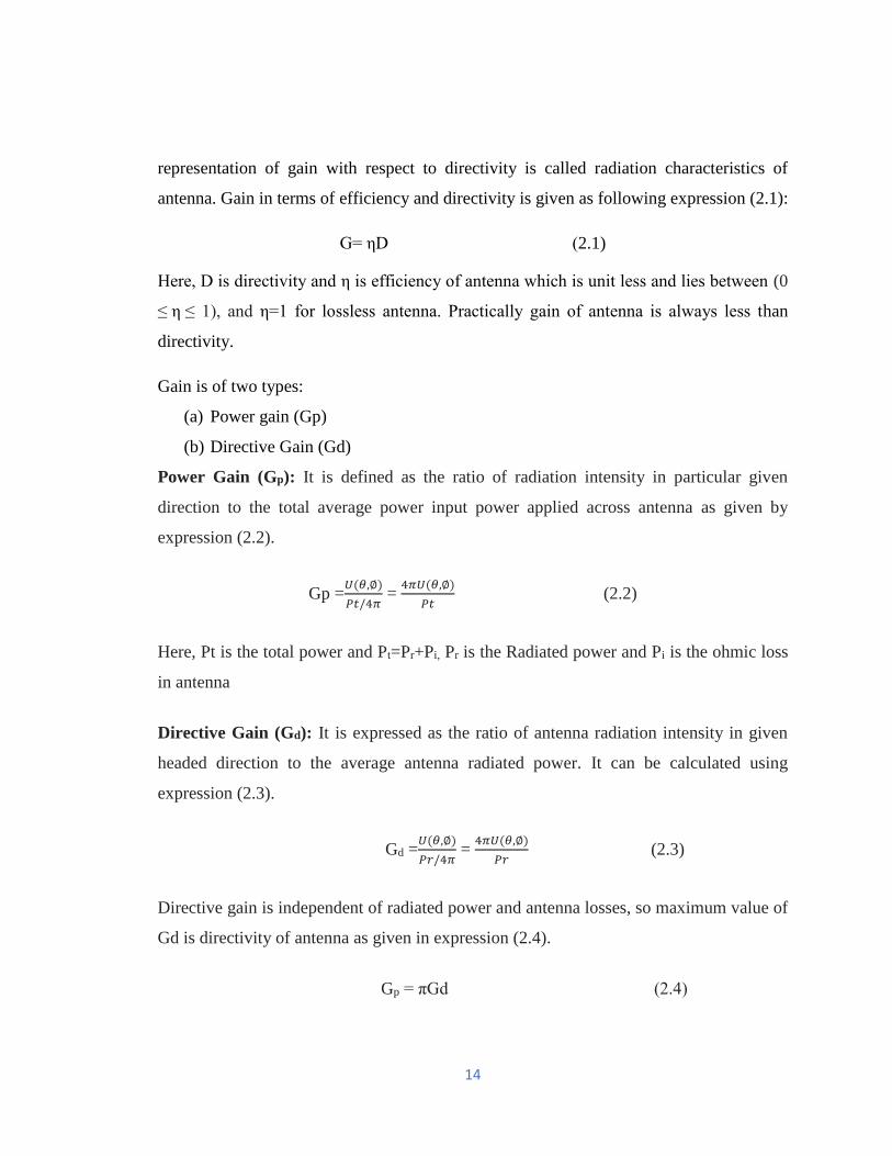
2.2.1 Antenna Gain: Antenna gain is defined as the ability of antenna to transmit and
radiate in particular direction as compared to isotropic antenna. Directional antenna gives
better performance in one direction than isotropic antenna. For transmitting antenna, gains
are the factor of input energy conversion into radio waves in one direction and for receiving
antenna gain defines how much radio frequency wave are converted into electrical signal.
Antenna gain is basically functioning of antenna efficiency and directivity. Graphical
14
representation of gain with respect to directivity is called radiation characteristics of
antenna. Gain in terms of efficiency and directivity is given as following expression (2.1):
G= ηD (2.1)
Here, D is directivity and η is efficiency of antenna which is unit less and lies between (0
≤ η ≤ 1), and η=1 for lossless antenna. Practically gain of antenna is always less than
directivity.
Gain is of two types:
(a) Power gain (Gp)
(b) Directive Gain (Gd)
Power Gain (Gp): It is defined as the ratio of radiation intensity in particular given
direction to the total average power input power applied across antenna as given by
expression (2.2).
Gp =𝑈(𝜃,∅)
𝑃𝑡/4𝜋 =
4𝜋𝑈(𝜃,∅)
𝑃𝑡 (2.2)
Here, Pt is the total power and Pt=Pr+Pi, Pr is the Radiated power and Pi is the ohmic loss
in antenna
Directive Gain (Gd): It is expressed as the ratio of antenna radiation intensity in given
headed direction to the average antenna radiated power. It can be calculated using
expression (2.3).
Gd =𝑈(𝜃,∅)
𝑃𝑟/4𝜋 =
4𝜋𝑈(𝜃,∅)
𝑃𝑟 (2.3)
Directive gain is independent of radiated power and antenna losses, so maximum value of
Gd is directivity of antenna as given in expression (2.4).
Gp = πGd (2.4)
15
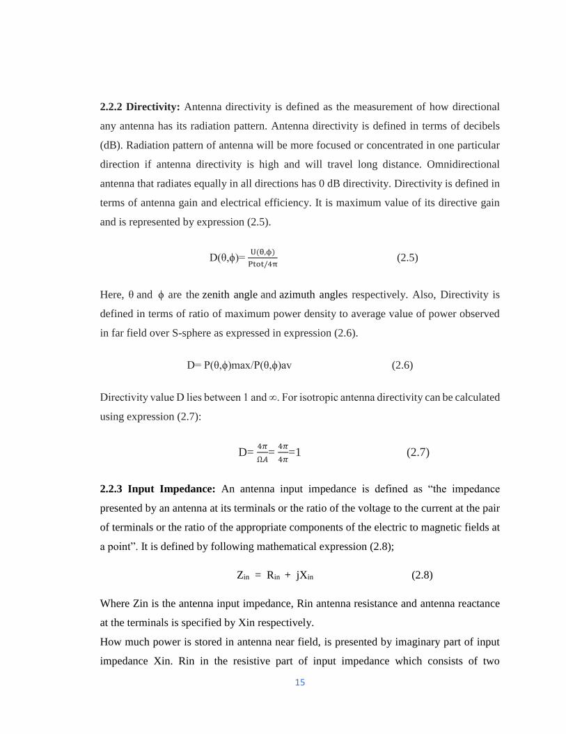
2.2.2 Directivity: Antenna directivity is defined as the measurement of how directional
any antenna has its radiation pattern. Antenna directivity is defined in terms of decibels
(dB). Radiation pattern of antenna will be more focused or concentrated in one particular
direction if antenna directivity is high and will travel long distance. Omnidirectional
antenna that radiates equally in all directions has 0 dB directivity. Directivity is defined in
terms of antenna gain and electrical efficiency. It is maximum value of its directive gain
and is represented by expression (2.5).
D(θ,ϕ)= U(θ,ϕ)
Ptot/4π (2.5)
Here, θ and ϕ are the zenith angle and azimuth angles respectively. Also, Directivity is
defined in terms of ratio of maximum power density to average value of power observed
in far field over S-sphere as expressed in expression (2.6).
D= P(θ,ϕ)max/P(θ,ϕ)av (2.6)
Directivity value D lies between 1 and ∞. For isotropic antenna directivity can be calculated
using expression (2.7):
D= 4𝜋
Ω𝐴=
4𝜋
4𝜋=1 (2.7)
2.2.3 Input Impedance: An antenna input impedance is defined as “the impedance
presented by an antenna at its terminals or the ratio of the voltage to the current at the pair
of terminals or the ratio of the appropriate components of the electric to magnetic fields at
a point”. It is defined by following mathematical expression (2.8);
Zin = Rin + jXin (2.8)
Where Zin is the antenna input impedance, Rin antenna resistance and antenna reactance
at the terminals is specified by Xin respectively.
How much power is stored in antenna near field, is presented by imaginary part of input
impedance Xin. Rin in the resistive part of input impedance which consists of two
16
components further, Radiation resistance Rr and loss resistance RL. The actual power
radiated by antenna is the power associated with radiation resistance, and power dissipated
in terms of heat is the power loss due to dielectric or antenna conducting losses.
2.2.4 Return Loss: Return loss is the function of transmitted power and reflected power
in dB. It is mostly measured at the input of the coaxial cable connected to the antenna. If
Pt is the source transmitted power and Pr is the reflected power than ratio of Pr/Pt is termed
as return loss. Of return loss should be very small to transfer maximum power. Return loss
is mainly presented in negative and should be as large a negative number [31,32]. Large
negative is the value, good will be the return loss. Value for maximum power transfer the
return loss should be as small as possible. Return Loss is expressed in dB as expressed in
expression (2.9):
𝑅𝐿 (dB) = −20 log10 𝛤 (2.9)
Where | Γ | = is the reflection coefficient
2.2.5 Radiation Intensity: Radiation intensity is defined as power radiated rom antenna
with respect to per unit of solid angle U that is independent on that part of the sphere surface
in both horizontal and vertical planes. Antenna radiation intensity is related to beam
direction and beam efficiency in that direction. It is used to measure radiation from antenna
due to its independence on measurement range. Radiation intensity can be measured w.r.t
isotropic antenna and given by expression (2.10);
Radiation Intensity U=𝑊
4𝜋 (2.10)
By plotting radiation intensity with different directions radiation pattern can be achieved.
2.2.6 VSWR: Voltage Standing Wave Ratio parameter is used to measure how efficiently
antenna impedance is matched with transmission line to deliver maximum power. To
transfer maximum power between source and load, impedance of both terminals should be
matched. Also, when transmission line is not properly terminated, then travelling wave is
17
reflected back completely or partially at the termination end. So, the combination of these
incident and reflected waves give rise to voltage standing waves along the transmission
line. This ratio of maximum to minimum amplitude of voltage is called VSWR [4] as given
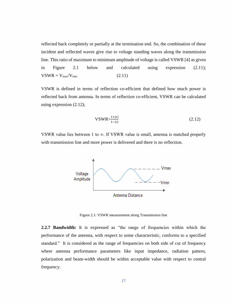
in Figure 2.1 below and calculated using expression (2.11);
VSWR = Vmax/Vmin (2.11)
VSWR is defined in terms of reflection co-efficient that defined how much power is
reflected back from antenna. In terms of reflection co-efficient, VSWR can be calculated
using expression (2.12);
VSWR=1+|ᴦ|
1−|ᴦ| (2.12)
VSWR value lies between 1 to ∞. If VSWR value is small, antenna is matched properly
with transmission line and more power is delivered and there is no reflection.
Figure 2.1: VSWR measurement along Transmission line
2.2.7 Bandwidth: It is expressed as “the range of frequencies within which the
performance of the antenna, with respect to some characteristic, conforms to a specified
standard.” It is considered as the range of frequencies on both side of cut of frequency
where antenna performance parameters like input impedance, radiation pattern,
polarization and beam-width should be within acceptable value with respect to central
frequency.
18
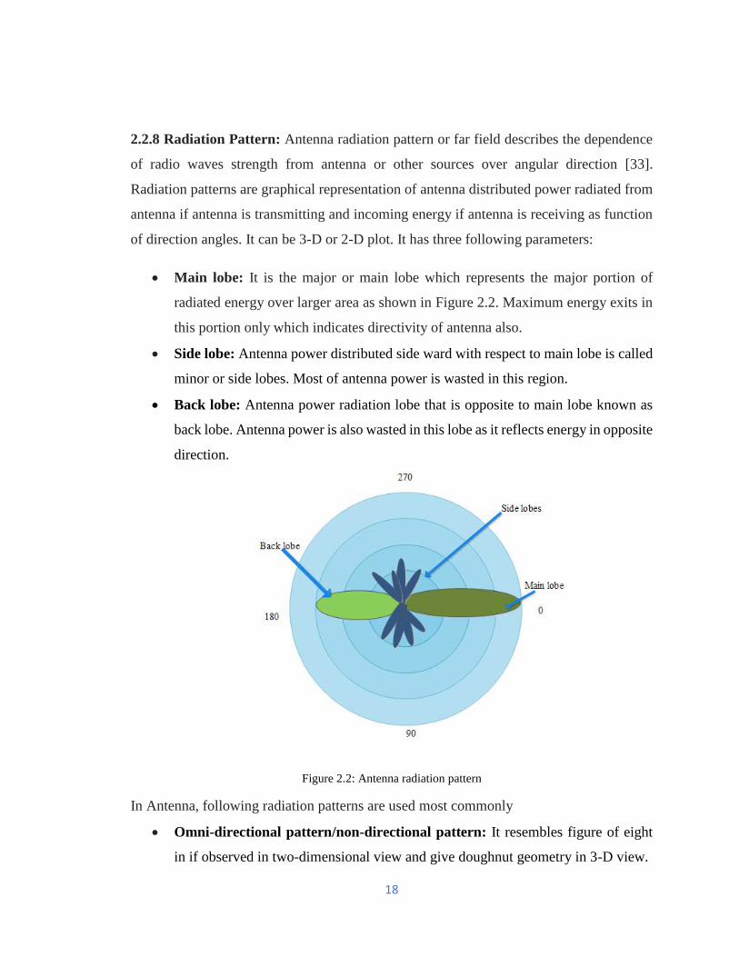
2.2.8 Radiation Pattern: Antenna radiation pattern or far field describes the dependence
of radio waves strength from antenna or other sources over angular direction [33].
Radiation patterns are graphical representation of antenna distributed power radiated from
antenna if antenna is transmitting and incoming energy if antenna is receiving as function
of direction angles. It can be 3-D or 2-D plot. It has three following parameters:
• Main lobe: It is the major or main lobe which represents the major portion of
radiated energy over larger area as shown in Figure 2.2. Maximum energy exits in
this portion only which indicates directivity of antenna also.
• Side lobe: Antenna power distributed side ward with respect to main lobe is called
minor or side lobes. Most of antenna power is wasted in this region.
• Back lobe: Antenna power radiation lobe that is opposite to main lobe known as
back lobe. Antenna power is also wasted in this lobe as it reflects energy in opposite
direction.
Figure 2.2: Antenna radiation pattern
In Antenna, following radiation patterns are used most commonly
• Omni-directional pattern/non-directional pattern: It resembles figure of eight
in if observed in two-dimensional view and give doughnut geometry in 3-D view.
19
• Pencil-beam pattern: The beam has a sharp directional pencil shaped pattern.
• Fan-beam pattern: The beam has a fan-shaped pattern.
2.3. INTRODUCTION TO MICRO-STRIP PATCH ANTENNA
Micro-strip patch antenna gain attention in wireless communication applications these
days. This antenna come in existence in 1953 and practically used in various applications
in 1970’s. They become highly useful due to circuit printed technology. Also, at the same
time, it’s less weight and simple profile make it more useful as compared to other antennas
like dipole, parabolic reflector for various applications like satellite, spacecraft, and mobile
applications. Micro-strip patch antenna is very simple in profile as they consist of metallic
area placed above the dielectric substrate and ground plane on other side.
Micro-strip antenna patch and ground materials generally consist of materials like copper
or gold. Antenna patch can be of different shapes like circular, square, rectangular,
triangular, semi-circular etc. Patch and feed line used to excite antenna are photo etched on
dielectric substrate material. Performance characteristics of patch antenna depends upon
the dielectric material used and physical dimensions of it.
Over conventional antenna, micro-strip patch antenna has many advantages and
applications. Conventional antennas are bulkier, integration problems and not able to
achieve multi band operations. Due to PCB (Printed Circuit Board) technology, micro-strip
antennas have planer surface, easy to integrated with microwave RF circuits, light in weight
and exhibits dual and multi band characteristics. These antennas are versatile in parameters
like resonant frequency, radiations and polarization. Also, different radiation patterns,
modes of operation and polarization can be obtained by integrating components like diodes,
shorting pins, adding loads between patch and ground plane. Instead of having numerous
advantages, it has several disadvantages like narrow bandwidth, low power handling, high
ohmic losses, less gain, unwanted radiations and low efficiency [33].
20
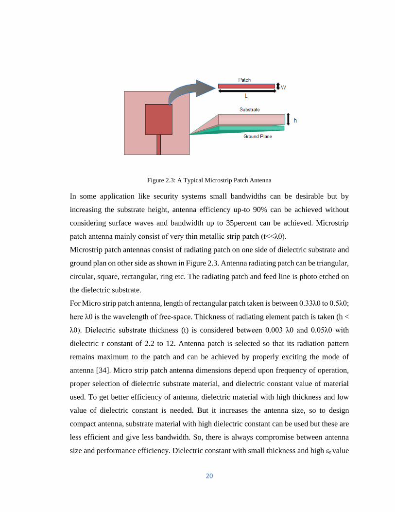
Figure 2.3: A Typical Microstrip Patch Antenna
In some application like security systems small bandwidths can be desirable but by
increasing the substrate height, antenna efficiency up-to 90% can be achieved without
considering surface waves and bandwidth up to 35percent can be achieved. Microstrip
patch antenna mainly consist of very thin metallic strip patch (t<<λ0).
Microstrip patch antennas consist of radiating patch on one side of dielectric substrate and
ground plan on other side as shown in Figure 2.3. Antenna radiating patch can be triangular,
circular, square, rectangular, ring etc. The radiating patch and feed line is photo etched on
the dielectric substrate.
For Micro strip patch antenna, length of rectangular patch taken is between 0.33λ0 to 0.5λ0;
here λ0 is the wavelength of free-space. Thickness of radiating element patch is taken (h <
λ0). Dielectric substrate thickness (t) is considered between 0.003 λ0 and 0.05λ0 with
dielectric r constant of 2.2 to 12. Antenna patch is selected so that its radiation pattern
remains maximum to the patch and can be achieved by properly exciting the mode of
antenna [34]. Micro strip patch antenna dimensions depend upon frequency of operation,
proper selection of dielectric substrate material, and dielectric constant value of material
used. To get better efficiency of antenna, dielectric material with high thickness and low
value of dielectric constant is needed. But it increases the antenna size, so to design
compact antenna, substrate material with high dielectric constant can be used but these are
less efficient and give less bandwidth. So, there is always compromise between antenna
size and performance efficiency. Dielectric constant with small thickness and high εr value
21
can be used for microwave circuits because tightly bound magnetic fields are needed to
reduce effect of un- wanted radiations and coupling and to achieve more compactness. Path
antenna analysis is done using transmission line, cavity or full wave methods. Among all
methods transmission method is easy but less accurate and cavity model method is more
accurate but difficult to analyse and more complex. Most accurate method is full wave
methods of analysis [34]. Due to finite dimensions of patch, antenna goes under fringing
effect from the edges. The amount of fringing is mainly function of antenna dimensions
and substrate height. In antenna for x-y plane, fringing is function of L/h and value of
substrate. Instead, of various advantages Micro strip patch antennas has some shortcomings
in terms of gain and bandwidth. Researchers are mainly focusing on different techniques
used to improve antenna gain and bandwidth. Applications of micro-strip Patch antenna in
wireless applications is also depicts in Figure 2.4 below.
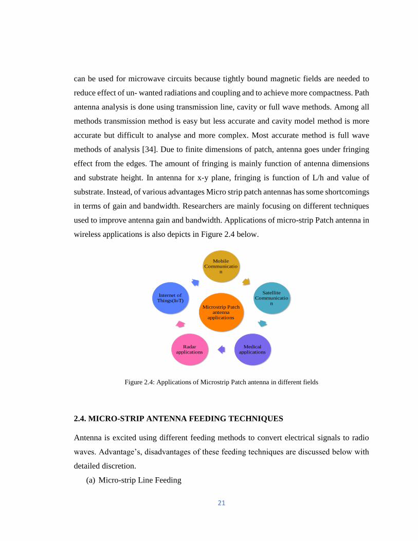
Figure 2.4: Applications of Microstrip Patch antenna in different fields
2.4. MICRO-STRIP ANTENNA FEEDING TECHNIQUES
Antenna is excited using different feeding methods to convert electrical signals to radio
waves. Advantage’s, disadvantages of these feeding techniques are discussed below with
detailed discretion.
(a) Micro-strip Line Feeding
Microstrip Patch antenna
applications
Mobile Communicatio
n
Satellite Communicatio
n
Medical applications
Radar applications
Internet of Things(IoT)
22
(b) Probe Coupling
(c) Aperture Coupled Feed
(d) Proximity Coupling feed
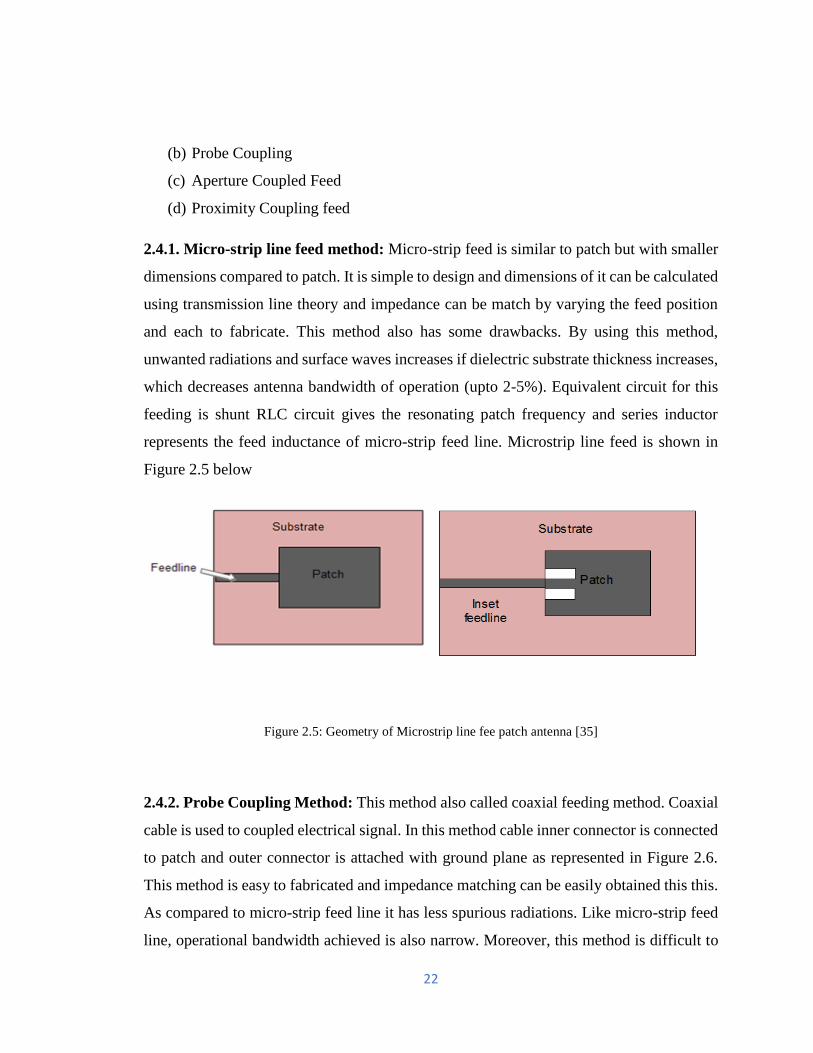
2.4.1. Micro-strip line feed method: Micro-strip feed is similar to patch but with smaller
dimensions compared to patch. It is simple to design and dimensions of it can be calculated
using transmission line theory and impedance can be match by varying the feed position
and each to fabricate. This method also has some drawbacks. By using this method,
unwanted radiations and surface waves increases if dielectric substrate thickness increases,
which decreases antenna bandwidth of operation (upto 2-5%). Equivalent circuit for this
feeding is shunt RLC circuit gives the resonating patch frequency and series inductor
represents the feed inductance of micro-strip feed line. Microstrip line feed is shown in
Figure 2.5 below
Figure 2.5: Geometry of Microstrip line fee patch antenna [35]
2.4.2. Probe Coupling Method: This method also called coaxial feeding method. Coaxial
cable is used to coupled electrical signal. In this method cable inner connector is connected
to patch and outer connector is attached with ground plane as represented in Figure 2.6.
This method is easy to fabricated and impedance matching can be easily obtained this this.
As compared to micro-strip feed line it has less spurious radiations. Like micro-strip feed
line, operational bandwidth achieved is also narrow. Moreover, this method is difficult to
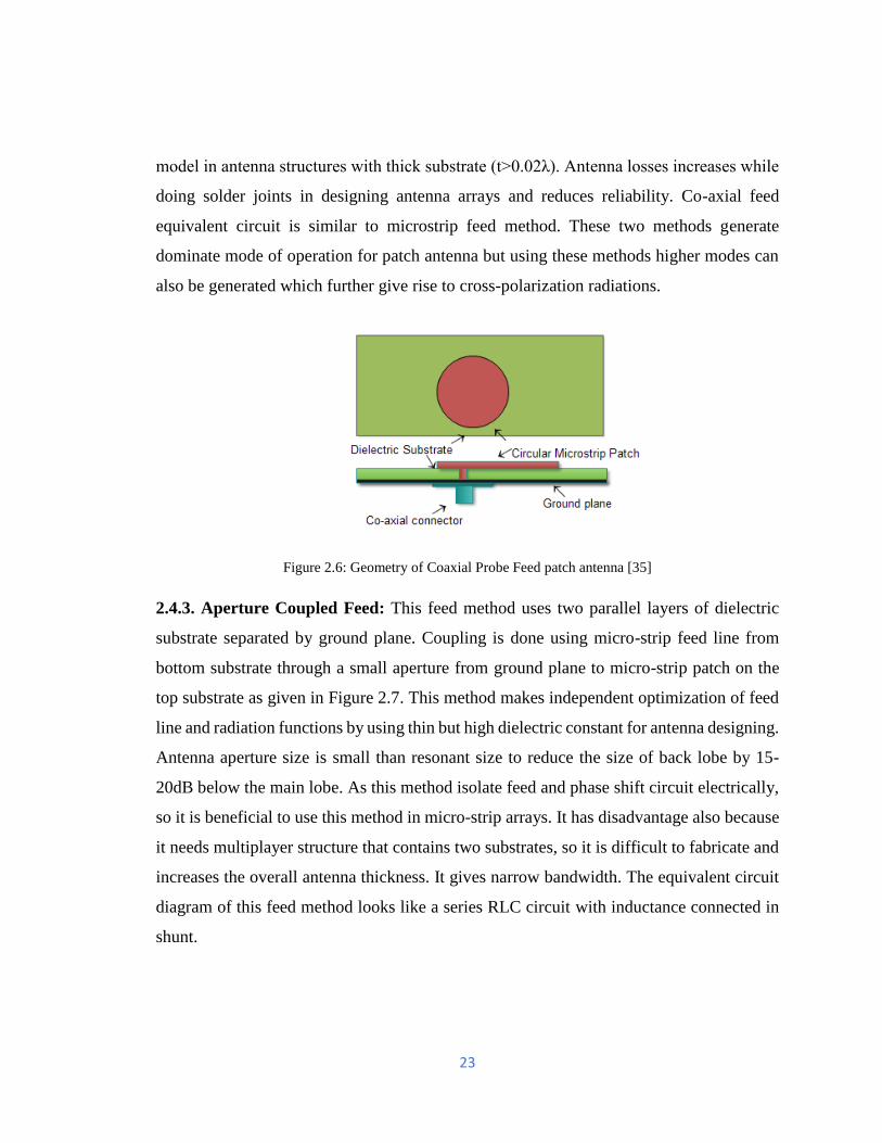
23
model in antenna structures with thick substrate (t>0.02λ). Antenna losses increases while
doing solder joints in designing antenna arrays and reduces reliability. Co-axial feed
equivalent circuit is similar to microstrip feed method. These two methods generate
dominate mode of operation for patch antenna but using these methods higher modes can
also be generated which further give rise to cross-polarization radiations.
Figure 2.6: Geometry of Coaxial Probe Feed patch antenna [35]
2.4.3. Aperture Coupled Feed: This feed method uses two parallel layers of dielectric
substrate separated by ground plane. Coupling is done using micro-strip feed line from
bottom substrate through a small aperture from ground plane to micro-strip patch on the
top substrate as given in Figure 2.7. This method makes independent optimization of feed
line and radiation functions by using thin but high dielectric constant for antenna designing.
Antenna aperture size is small than resonant size to reduce the size of back lobe by 15-
20dB below the main lobe. As this method isolate feed and phase shift circuit electrically,
so it is beneficial to use this method in micro-strip arrays. It has disadvantage also because
it needs multiplayer structure that contains two substrates, so it is difficult to fabricate and
increases the overall antenna thickness. It gives narrow bandwidth. The equivalent circuit
diagram of this feed method looks like a series RLC circuit with inductance connected in
shunt.
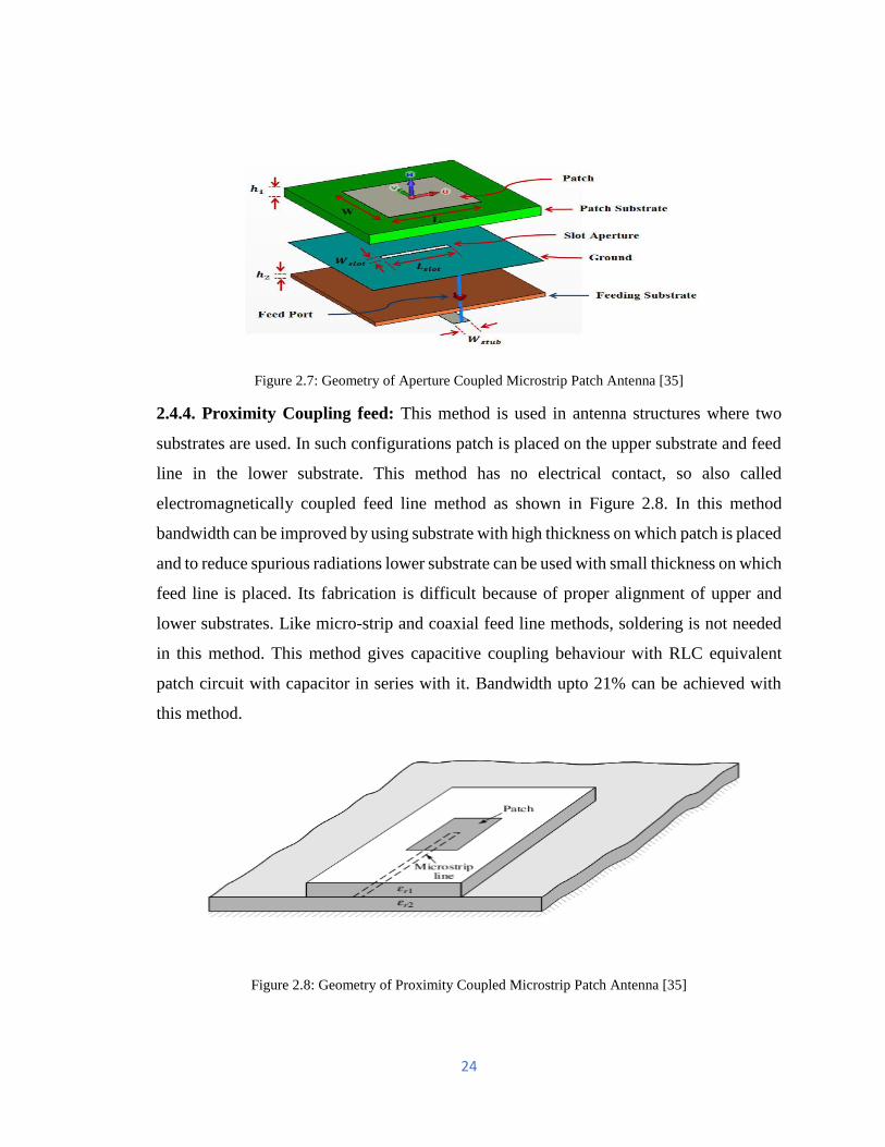
24
Figure 2.7: Geometry of Aperture Coupled Microstrip Patch Antenna [35]
2.4.4. Proximity Coupling feed: This method is used in antenna structures where two
substrates are used. In such configurations patch is placed on the upper substrate and feed
line in the lower substrate. This method has no electrical contact, so also called
electromagnetically coupled feed line method as shown in Figure 2.8. In this method
bandwidth can be improved by using substrate with high thickness on which patch is placed
and to reduce spurious radiations lower substrate can be used with small thickness on which
feed line is placed. Its fabrication is difficult because of proper alignment of upper and
lower substrates. Like micro-strip and coaxial feed line methods, soldering is not needed
in this method. This method gives capacitive coupling behaviour with RLC equivalent
patch circuit with capacitor in series with it. Bandwidth upto 21% can be achieved with
this method.
Figure 2.8: Geometry of Proximity Coupled Microstrip Patch Antenna [35]
25
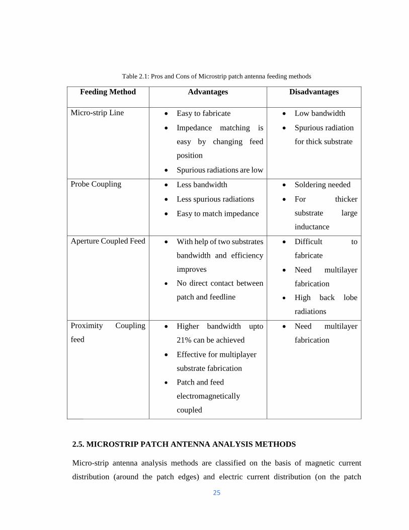
Table 2.1: Pros and Cons of Microstrip patch antenna feeding methods
Feeding Method Advantages Disadvantages
Micro-strip Line • Easy to fabricate
• Impedance matching is
easy by changing feed
position
• Spurious radiations are low
• Low bandwidth
• Spurious radiation
for thick substrate
Probe Coupling
• Less bandwidth
• Less spurious radiations
• Easy to match impedance
• Soldering needed
• For thicker
substrate large
inductance
Aperture Coupled Feed
• With help of two substrates
bandwidth and efficiency
improves
• No direct contact between
patch and feedline
• Difficult to
fabricate
• Need multilayer
fabrication
• High back lobe
radiations
Proximity Coupling
feed
• Higher bandwidth upto
21% can be achieved
• Effective for multiplayer
substrate fabrication
• Patch and feed
electromagnetically
coupled
• Need multilayer
fabrication
2.5. MICROSTRIP PATCH ANTENNA ANALYSIS METHODS
Micro-strip antenna analysis methods are classified on the basis of magnetic current
distribution (around the patch edges) and electric current distribution (on the patch
26
conductor and the ground plane). On basis of magnetic current distribution there are three
techniques:
• ·The transmission line model
• ·The cavity models
• The MNM (Multiport Network Model)
Microstrip patch antenna analysis can be done using different methods like transmission
line model, full wave method and cavity model method as given in Figure 2.9. Among all
these methods, transmission line analysis method is the simplest method, easy to model
antenna but this is less accurate method. Cavity method is more accurate as compared to
transmission line method, more flexible and provides good insight physically but more
complex in nature. More versatile and accurate is full wave method. On basis of electric
current distribution there are three techniques:
• The method of moments (MoM)
• The finite-element method (FEM)
• The spectral domain technique (SDT)
• The finite-difference time domain (FDTD) method
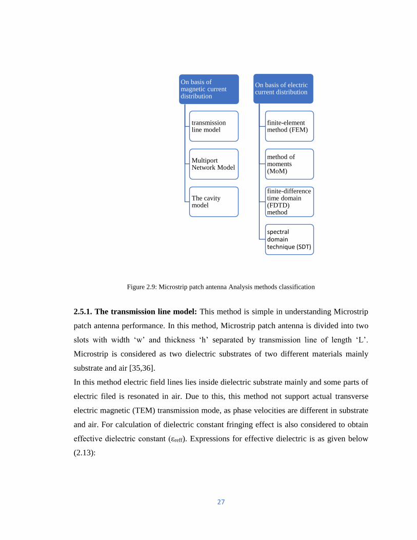
27
Figure 2.9: Microstrip patch antenna Analysis methods classification
2.5.1. The transmission line model: This method is simple in understanding Microstrip
patch antenna performance. In this method, Microstrip patch antenna is divided into two
slots with width ‘w’ and thickness ‘h’ separated by transmission line of length ‘L’.
Microstrip is considered as two dielectric substrates of two different materials mainly
substrate and air [35,36].
In this method electric field lines lies inside dielectric substrate mainly and some parts of
electric filed is resonated in air. Due to this, this method not support actual transverse
electric magnetic (TEM) transmission mode, as phase velocities are different in substrate
and air. For calculation of dielectric constant fringing effect is also considered to obtain
effective dielectric constant (εreff). Expressions for effective dielectric is as given below
(2.13):
On basis of magnetic current distribution
transmission line model
Multiport Network Model
The cavity model
On basis of electric current distribution
finite-element method (FEM)
method of moments (MoM)
finite-difference time domain (FDTD) method
spectral domain technique (SDT)

28
εreff =𝜀𝑟𝑒𝑓𝑓+1
2 +
𝜀𝑟𝑒𝑓𝑓−1
2[1 +
12ℎ
𝑤]
−1/2
(2.13)
Where εreff = Effective dielectric constant, εr = Dielectric constant of substrate, h = Height
of the dielectric substrate, w = Width of the patch
2.5.2. Cavity model: In this method of analysis, area between the patch and ground plane
of antenna is treated as cavity which is surrounded by magnetic walls and electric walls
around the periphery and from top and bottom respectively. These fields are uniform along
substrate thickness because thin dielectric substrates are used [36,37]. For different patch
shapes like rectangular, triangular and circular shapes, fields are calculated as integration
of various resonant modes of 2D resonator. Antenna effective dimensions should remain
larger than physical dimensions, for that fringing fields are considered around patch
periphery. Dielectric substrate loss tangent is calculated so that it incorporates conductor
losses and antenna radiations. Equivalent magnetic currents are used to calculate far field
and antenna radiated power around antenna periphery. The fringing field and antenna
radiated power are considered only at edges not inside the cavity.
2.5.3. Multiport Network Model (MNM): This method is the extension of cavity model
method [38,39]. In this method, electromagnetic fields below the patch and outside patch
are modelled individually. The antenna patch is considered as 2D planer network with
multiple ports located around its boundary. From 2D green’s function multiport impedance
patch matrix is obtained. By adding an edge equivalent admittance network, the fringing
fields along patch boundary and radiated fields are calculated. After that segmentation
method is used to find overall impedance matrix. Voltage distribution around periphery is
used to calculate radiation fields.
These methods are used for regular patch geometries but for complex geometries following
methods are used.
2.5.4. Method of moments (MoM): In this MoM method two types of currents are used
for antenna modelling i.e. surface currents and polarization currents. Surface currents are
used to model patch and polarization currents available inside dielectric slab are mainly
29
used for field modelling. To formulate unknown currents of Microstrip patches, feed lines
and their images in the ground plane, an integral equation is used [40]. These equations are
solved using computers after converting them into algebraic equations. This method
provides more exact solution because in this fringing fields outside the physical periphery
of 2D patch is also considered.
2.5.5. Finite-element method (FEM): FEM method is mainly used for volumetric
configurations. In this process, the area of interest is cut down into small number of finite
surfaces or volume elements on basis of planar or volumetric structures to be analysed [41].
These divided discrete elements, also called finite elements can be of any properly defined
geometrical structures like triangular elements for planar configurations and for 3-D
configurations elements used are tetrahedral and prismatic which are more suitable for
curved geometry also. In this method, integration of some basic functions is done over
entire conducting patch that is divided into different number of subsections. To solve wave
equations by inhomogeneous is done by dividing it into two boundary value problems, first
is Laplace’s equation and second with inhomogeneous wave expression with
inhomogeneous and homogeneous boundary respectively [42].
2.5.6. Spectral domain technique (SDT): In this method, in plane of Microstrip patch
substrate, a 2-D Fourier transform with two orthogonal directions are employed. Also,
boundary conditions are applied in Fourier transform plane. The current distribution on the
conducting patch is expanded in terms of chosen basis functions, and the resulting matrix
equation is solved to evaluate the electric current distribution on the conducting patch and
the equivalent magnetic current distribution on the surrounding substrate surface. The
various parameters of the antennas are then evaluated [43].
2.5.7. Finite Difference Time Domain (FDTD): This method is highly suitable for
Microstrip antennas because it can easily model various structural in-homogeneities
occurred in these configurations. In this method, time and spatial grid for electric and
magnetic fields are generated to find the solution. For spatial discretization, three Cartesian
co-ordinates are considered to be same. With antenna boundary configuration E-cell edges
30
are aligned and it is assumed that H-fields are located at the centre of each E-cell. Each cell
keep information about characteristics of material and cells with the source are excited
using suitable excitation function that propagates along the structure. Time variations of
electric and magnetic fields are calculated at desired locations. The current is calculated by
an integral loop of the magnetic field which surrounds the conductor, where Fourier
transform provides a frequency response.
These methods, which are based on electric current distribution over the patch and ground
plane conductor gives accurate results for any arbitrary shaped antenna structures but these
methods are time consuming and provide less of physical understanding needed for antenna
designing but can be useful to plot patch current distributions.
2.6. SUMMARY
This chapter deals exclusively with the fundamental of Antenna and Transmission line
theory and antenna performance parameters with mathematical expression carried out for
analysis. Further, it explains in detail about Microstrip patch antenna basic structure, its
advantages and disadvantages. Also, different types of feeding methods used to improve
gain and bandwidth of patch antenna with different analysis methods used in Antenna
simulation software’s like HFSS, CST. To sum up, this chapters laid emphasis on
microstrip patch antennas.
31
CHAPTER-3
STATE OF ART
3.1. INTRODUCTION
With the recent developments in wireless communication systems demand for higher data
rate and at very high-speed increased day by day which results in evolution of WIMAX,
WI-FI, Bluetooth, UWB and mobile communication technology at high frequency bands.
Personal communication devices aim to provide audio, video and data communication at
very high rate and efficiently at anytime and anywhere in the world. To full fill all these
requirements the communication terminal antenna must full-fill the requirements to
sufficiently cover the possible operating bands. The key issue is to develop a compact and
simple antenna with wideband characteristics. So various techniques to enhance the
bandwidth, radiation pattern, return loss, Gain and directivity of antennas has been studied
in the literature survey.
3.2. LITERATURE REVIEW
Young-Bae Jung et al. [44] describes triband antenna for Ka-K band. Author uses a
Cassegrain reflector with integrated feeder for the k band to design modified hybrid
antenna (HA). A microstrip antenna is used that consist of four linear sub-arrays and placed
on the sub-reflector of the HA for Ku band services to provide high gain and to achieve
rapid 2-D scanning ability at cheap cost for satellite applications. So, antenna is designed
using a novel beam- steering through sub-reflector i.e. rotational and flat. A hexagonal
structure is designed that uses feeder consist of 20 dual band horn elements those provide
dual polarization also to maximise the efficiency. To reduce size, transmitter and receivers
are connected with feeder horn elements. Antenna was tested for both indoor and outdoor
environment and provides an EIRP of 55.2dBW and GT of 16.8dB for k band and 7.6dB
for ku band.
32
As microstrip patch antenna has narrow bandwidth that is serious drawback of microstrip
patch antenna. Author Yikai Chen et al. [45] uses concept of distributed L and C circuit to
enhance bandwidth of E-shaped conventional patch antenna. In conventional E shape
antenna, low inductance occurs due to probe fed, so LC circuit is used to reduce the
thickness of air acting as substrate. A new resonant frequency introduced by LC circuit,
near to that of E-shape increases the bandwidth of antenna without compensating the gain.
Designed antenna operates on AMPS band from 824 to 894GHz frequency band.
Simulation results shows that designed antenna has an impedance over 9% for Voltage
Standing Wave Ratio (VSWR) over the frequency band is less than 2 but shows satisfactory
performance in radiation pattern within the operated bandwidth.
Hussein Attiam et al. [46] discusses that microstrip antenna gain can be enhanced under
some resonance conditions when antenna is covered with superstrate with proper distance
in free space. Resonance conditions can be deduced by using proper transmission method
and the cavity model to achieve the highest gain. Resonance effect can be changed by
adjusting the spacing between antenna’s superstrate and substrate and by varying thickness
of the substrate. Depending upon these resonant lengths the permittivity, permeability and
superstrate are determined and characteristics impedance can also be determined of the
multilayer structure. Antenna performance is verified using simulation results and
analytical methods also. From simulation results author concludes that proposed method
enhances the antenna performance by 50% when compared to previous methods.
In research article [47] Ramona Cosmina Hadarig et al. proposes use of electromagnetic
band-gap (EBG) structures and artificial magnetic conductors (AMC) due to their
advantages use to improve antenna performance like better efficiency, high gain, and low
back lobe and less side lobe levels. He designed antenna using combination of EBG with
patch antenna in single layer and combination of AMC with patch antenna in two different
layers. Due to more compactness and robustness antenna is compatible with plane antenna
fabrication technology because it not needs via holes. Proposed antenna works in RFID
2.48GHz frequency band, also it shows better radiation properties without increasing
33
antenna size and thickness. Proposed antenna provided bandwidth of 34MHz with EGB
and of 46MHz with AMC over 23MHz for simple antenna, as well as gain improved from
4.6dB to 5.576 dB over the operating frequency band.
Feeding methods play important role as antenna efficiency also depends upon how power
is transferred to the radiating element directly or indirectly. In research article [48]
Soumyojit Sinha et al. describe advantages of microstrip antenna as low cost, low profile
and conformal antenna. Different methods are used for antenna excitation like by coaxial
probe and by microstrip line directly. Various indirect methods for excitation are also used
like aperture coupling and electromagnetic coupling as there is not direct metallic contact
between the patch and the feed line. Input impedance of antenna totally depends on type of
feeding method used. So, author designed a rectangular patch antenna that works at 2.21
GHz frequency band using 1E3D simulator. Antenna feeding is done using probe. From
simulation results antenna performs well in terms of radiation for wireless applications like
mobile handheld radios, global positioning systems (GPS), radar for missiles.
To improve antenna bandwidth Y. Sung in [49] proposes printed wide slot line fed compact
microstrip patch antenna with parasitic centre patch to further increase the bandwidth of
conventional patch antenna. A 50ohm microstrip feed line is used to excite slot and rotated
square slot resonator is considered as basic patch design. Resonator shows two frequencies
i.e.f1 low resonant and f2 high resonant frequency. From simulation results author
investigates that low resonance frequency deceases and high resonant frequency increases
by placing parasitic patch in centre of rotated square slot. Simulation results show
improvement in bandwidth more than 1GHz. Also proposed structure provides impedance
bandwidth of 80% for 2.23 to 5.35 GHz bandwidth. Antenna covers WLAN 2.4, 5.2, 5.8
GHz bands and WiMax 2.5, 3.5, 5.5 GHz bands.
To improve microstrip antenna bandwidth a pair of parasitic patches is used by S. T. Fan
et al. in [50]. Antenna dimensions taken are 37mm by 37mm, and fabricated using FR4
material with thickness of 1.6mm, relative permittivity of 4.4. To improve band, microstrip
feed with 16 mm length and width 2.5 mm is used with a pair of semi-circular parasitic
34
patches on both sides of it to provide additional resonance in the circuit. To provide strong
coupling with feed line, gap of 0.5mm is maintained between patch and feed line. Antenna
design is simple and easy in fabrication. Simulation results shows that bandwidth
improvement is 136% for VSWR less than 2 for 2.1 to 11.1 GHz bandwidth. From
simulation results the proposed antennas can be used for ultra-wideband modern wireless
Communication applications.
P. A. Ambresh et al. [51] proposed a new micro-strip patch antenna with reduces size using
FR4 dielectric substrate with slots for wireless applications. Proposed antenna works at
two resonant frequencies 3.55 GHz and 4.99 GHz. From simulation results antenna shows
18.2% compactness for 270MHZ impedance bandwidth. Antenna shows very good
performance in terms of return loss (RL) upto -36.14dB with Voltage Standing Wave ratio
less than 2. Author concludes from results that antenna show better performance with linear
polarization and also broadside radiation pattern is achieved with less cross polarization.
Syeda Fizzah Jilani et al. [52] proposed microstrip rectangular patch antenna with fractal
design. Basically, fractal design is used to enhance the gain and bandwidth of microstrip
patch antenna by implementing Star shaped patches at two sides and four corners of
conventional microstrip patch antenna to overcome the limitations of low bandwidth and
low gain of microstrip antenna. Antenna design is simple and easy to fabricate. Designed
antenna works on 10GHz and fractal geometry enhance the gain from 5.479dB to 11dB
and improves bandwidth from 550MHz to 5GHz as compared to conventional rectangular
patch antenna. According to IEEE standards antenna works in X-band and Ku band. The
side lobes in radiation pattern are reduced due to concept of proposed slots in design and
also improve gain and directivity of antenna. Proposed antenna also used for radar,
aerospace, satellites and communication systems.
Nitin Saluja et al. [53] design and fabricate planer inverted F-antenna using two folded
edges based on fractal geometry which shows multi band behaviours. From proposed
antenna, two frequency bands are achieved at lower and higher frequencies i.e. 2.25 to
2.863GHz and 4.81to 6.21GHz respectively. Impedance bandwidth obtained is 613MHz
35
i.e. 25% at lower band and 1400MHz which is 26.4% at high frequency band which shows
wide bandwidth. At low frequency band with centre frequency 2,4GHz maximum gain
achieved is 3.8dBi and 7.2dBi for cut off frequency of 5.3GHz for high frequency band.
Antenna is compact in size with overall dimensions of 19.83 x 19.8 mm2. To achieve more
compactness in design, antenna patch is folded under itself. The antenna structure is best
suited for Wi-Fi, LTE, WiMAX, and WLAN applications for mobile phone device.
Swaraj Panusa et al. [54] presents quad band H-slot microstrip patch antenna for WiMax
applications. Antenna performance is analysed using HFSS simulator in terms of gain,
return loss, radiation pattern, VSWR etc. Antenna shows multi band properties by just
etching H-shape slot on patch and easy in fabrication. FR4 epoxy substrate is used with
dielectric constant of 4.1 and coaxial technique is used for antenna feeding. Four frequency
bands 3.41 to 3.51 GHz, 4.64 to 4.75GHz, 5.45 to 5.63 GHz and 6.38 to 6.50 GHz are
covered by H-slot patch antenna. Maximum return loss is enhanced by antenna by -
16.92dB at 3.46 GHz, -18 dB at 4.73 GHz, -17.50 dB at 5.55 GHz and -17.45 dB at 6.45
GHz frequencies respectively that is better enough for WiMAX applications. Radiation
characteristics of proposed antenna are also good, so it can be used for multi band wireless
applications also.
Lei Chen et al. [55] proposed circularly polarized wideband antenna with wide beam-width
for S-band satellite communications. Author uses modified fork shaped inverted L-feed
with stacked patches to improve the impedance bandwidth. To achieve wide beam-width
concept of semi-open metal cavity is used. Simulation results shows that reflection co-
efficient is less than -10dB, bandwidth is 30.1%, axial ratio less than 3db, half-power beam-
width (HPBW) less than 100 degrees with gain of 3dbi. From experimental results antenna
shows better performance in terms of circular polarization, impedance matching, and wide
beam-width characteristics.
Eun-cheol Choi et al. [56] proposed a turnstile S-Band antenna using parasitic elements
with cylindrical arrays and uses power divider network for feeding. Antenna performance
is analysed in terms of beamwidth, gain, axial-ratio (AR), and radiation pattern. The desired
36
frequencies can be achieved by adjusting the height, locations and number of cylindrical
parasitic elements surrounding the bowtie shaped dipoles. Simulation results shows
antenna beamwidth of -3dB, Axial ratio (AR) of 5dB and stable peak gain of 7.6dBi and
bandwidth ranging from 2.02GHz to 2.29GHz with circular polarization. Antenna shows
enhanced beamwidth, due to this antenna can be used in C–band satellite communication
applications.
Jayarenjini. N et.al [57] purposes Dual Polarized micro-strip Fractal Patch Antenna for S-
band applications that operates in 2 to 4 GHz frequency band for S-band. Author mainly
uses the concept of fractal geometry to improve the bandwidth and to reduce isolation.
Proposed antenna shows improved isolation and isolation loss is reduced by a factor of
15dB. One of the disadvantages of dual Polarized micro-strip Fractal Patch Antenna is
reduced gain. The proposed antenna is used in applications like weather radars,
communication satellite and wireless communications.
Mohammed N. Shakib et al. [58] proposed stacked low-profile antenna for UWB
applications. Antenna contains three patches. One patch is angularly folded at 30 degrees
also called bottom patch, middle patch with T-Shape and strip loaded patch as a top patch.
The T-patch and angularly folded patch are combined together to achieve wide bandwidth.
Author uses the shorting wall concept to minimize the antenna size further. Impedance
bandwidth is improved using electromagnetic coupling between strip loaded patch antenna
and T-shapes antenna. Considered dimensions of antenna are 0.12λ x 0.14 λ x 0.08 λ, here
λ is the lowest operating frequency wavelength. From simulation results author analyse
that bandwidth of antenna is 107.46% for frequency band 3.1 to 10.3GHz. Antenna
performs well in gain, radiation pattern and provides low delay variations in the designed
frequency bands. Due to these entire advantage’s antenna is used for UWB applications.
In paper [59] Amanpreet Kaur et al. proposed a microstrip patch antenna using defected
ground structure concept for wireless applications like LAN and UWB. Fractal shaped used
in Sierpinski with aperture coupling feeding method. In antenna designing, author uses two
37
layers stacked on each other of FR4 substrate material with patch contains Sierpinski fractal
design on it. This complete structure further contains third layer at bottom of FR4 material,
through which antenna is feeded with stub line at the bottom with ground layer on its top.
To get wide antenna behaviour, cross type structure is cut from top ground layer. Designed
antenna showed multi band behaviour and resonated on two different bands 4.75 to
5.38GHz and 6.8 to 7.2GHz with bandwidth of 630MHz and 400MHz respectively.
Antenna has very good gain of 5.85 dB and 9.5 dB for these operating frequencies.
Proposed structure works for IEEE 802.11 (5.15 to 5.35GHz) band, covers two different
UWB spectrum 4750 to 5280MHz and radio astronomy frequency range from 5010 to
5030MHz. Antenna is designed and simulated using CST simulation software and tested
using VNA tester.
Microstrip patch antenna gain is enhanced by M. T. Islam et al. in article [60] by using
concept of parasitic patches. Antenna design consists of a rectangular parasitic strip at some
distance from another rectangular strip, which contains four V-shaped slits of asymmetric
structure at each corner of patch. For antenna manufacturing, Rogers’s substrate material
with relative permittivity of 2.2 with thickness 1.57mm is used. Antenna is circularly
polarized, and provides high gain for HORYU-IV S-band Nano-satellite applications for
low earth orbit (LEO). It provides return loss of -10db for 2.24 to 2.3GHz bandwidth with
3db AR and gain of 7.29dBi.
Faisel Tubbal et al. [61] studied the effect of CubSat body on antenna performance using
Coplanar Wave Guide (CPW) feed, square shaped slot and Shorted patch antenna using
HFSS simulator. From simulation results author concludes that performance of shorter
patch antenna is better than CPW-feed antenna as shorter patch antenna provides high gain
and wider bandwidth as compared to CPW feed antenna. Author again compares the
performance of both antennas after re-dimensioning by shifting their resonant frequencies
at 2.45GHz with help of quasi Newton algorithm to make use of both antennas in
unlicensed ISM band. Proposed antenna, at frequency of 2.45 GHz for S-band simulation
38
results shows that each modified antenna provides return loss below -10dB. Modified
CPW feed antenna provides gain of 2.52dB at 2.45 GHz resonant frequency.
Author in [62] Mehr-e-Munir et al. uses concept of slots in ground for antenna size
reduction and used patch slot method for multi band operation. By introducing slots in the
patch also reduces the size of antenna. Antenna is fabricated using FR4 substrate with
dielectric permittivity of 4.1. Results are simulated using Computer Simulation
Technology (CST) simulator in term of Radiation efficiency, return loss and gain of
antenna. Performance of designed antenna is compared with conventional micro-strip
patch antenna for operating frequencies 2606MHz, 2807MHz, 4200MHz, 6050MHz and
7420MHz. From simulation results author concludes that slotted antenna is more compact
in size as compared to conventional antenna. Due to this proposed antenna is used for S-
Band, C-band and mobile applications.
Markus H. Novak et al. [63] presents tightly coupled dipole array (TCDA) an ultra-
wideband antenna to support multiple satellite communication band at the same time.
Antenna is very helpful in weight reduction as it replaces multiple antennas. Array is
initially designed for operation across UHF, S, L and lower C-band for frequency 0.6 to
3.6GHz for easy of fabrication and more emphasis is given on dual –linear polarization.
Antenna provides more spectral efficiency because intermediate frequency is reused for
inter-satellite communication. Designed antenna array achieves a bandwidth of 6:1 for
VSWR less than 1.8. Author presents TCDA design for operation at frequency bands like
S-band, C-band, X-band and Ku bands (3 to 18GHz). From simulation results author
concludes that antenna performs better with proposed design in terms of bandwidth
efficiency.
Qiang Liu et al. [64] proposed double band circularly polarized (CP) microstrip patch
antenna that works on 0.92 to 2.45 GHz frequency band. Proposed antenna is used for
hand-held radio-frequency identification (RFID) radar applications. The antenna design
contains two stacked patches further assembled with two vertical orthogonally placed
probes and wideband network with dual feed. Stacked concentric patches used to generate
39
resonance frequencies at lower and higher band. Dual feed two-way network generates
signals with same amplitude and with phase difference of 90 degrees; due to this antenna
covers both band 0.92 and 2.45GHz. Proposed antenna performance is compared with
conventional antenna. Size of proposed antenna is 110 ×110 mm with height of 6.6 mm
that is much compact than dual-band single port RFID directional Circular Polarized reader
antennas. Proposed antenna is designed using PCB technology. Cost is also less.
Simulation results shows return loss > 10dB, 3dB variations in gain axial ratio< 3dB for
0.91 to 0.93GHz and 2.4 to 2.57 GHz frequency band. Antenna works for both industrial
scientific and medical ISM and RFID radar applications.
To improve bandwidth of basic microstrip patch antenna Ajay Thatere et al. [65] presents
U-shaped structured patch antenna on FR4 substrate with two equal arms to overcome
bandwidth limitation of general microstrip antenna. Under the U-shaped patch antenna on
the ground surface a U-shape slot is introduced. Antenna performance is studied by
analysing the performance of effect of slot size and different shapes of ground plane on
antenna impedance bandwidth. With implementation of U-shaped slot maximum
impedance bandwidth of 13% is obtained for 5.1 to 5.8 GHz frequency bands. From
simulation results author concludes that antenna provides Voltage Standing Wave Ratio of
1.2 at desired frequency. Also, antenna size is small and simple in construction as compared
to coplanar parasitic and regular stacked antennas. Due to simple construction and small
size proposed antenna is highly suitable for wireless communication applications.
Suyang Shi et al. [66] propose a wideband miniaturized patch antenna with dual feed line
structure. To shorten the non-radiating side of antenna element, based on concept of
transversal signal interference the dual structure is used. Additional T-Shaped stub
resonator is introduced in design in order to improve the impedance bandwidth. From
simulation results author conclude that when compared to rectangular patch antenna,
proposed antenna show 32% improvement in size reduction and 17% enhancement in
bandwidth are achieved.
40
Pritam Singh Bakariya et al [67] present a microstrip patch antenna for multi band
applications using a proximity-coupled feed. Author uses concept of slotted ground plane
with proximity coupled feeding to get multi band operation. Proposed antenna consists of
defected ground plane, meandered microstrip feed and truncated rectangular patch with
rectangular slot. For antenna fabrication FR4 substrate is used with εr= 4.4 and thickness
t= 0.8mm. Proposed antenna operates in WiMax (3.3 to 3.7GHz), Bluetooth (2400 to 2485
MHz), LTE2300 (2300 to 2400 MHz), and WLAN two bands 5.15 to 5.35 GHz, and 5.725
to 5.825 GHz. Simulation results shows that antenna performance is good in terms of gain,
it provides constant gain on all operating bands and shows better radiation characteristics
for operating frequency range.
In research article [68] Vandana Satam et al. proposed dual element antenna for MIMO to
provide good isolation characteristics and enhanced gain by minimizing the effect of
mutual coupling. Antenna is designed using Defected ground structures with ‘I’ shape
vertical slot for 5.8GHz frequency bands used for MIMO wireless applications. Antenna is
designed using FR4 substrate with dimensions 50.54 mm × 21.29 mm. MIMO antenna
contains two symmetrical elements fed with insect feeding method. DGS concept is used
to enhance mutual coupling. Designed antenna provides return loss of -21.71dB for
wireless application and -27.95 dB for other operating bands with resonating frequency of
5.66GHz and 7.53GHz respectively. Proposed MIMO structure provides high gain of
6.05dBi. From simulation results author analyse that antenna can provide spatial diversity
and also enhance data rate capacity of wireless communication systems. Antenna performs
well in terms of gain and return loss.
Author B. R. Sanjeeva Reddy et al. in paper [69] proposed antenna for wireless
communications with Zigzag shaped structure using microstrip antenna with defected
ground. Antenna design consist of three steps: initially dual T-shaped slits are cut from
opposite sides of rectangular patch, secondly, a zigzag-shaped slit is cut from patch and
finally dumbbell- shaped defected ground plane with probe feeding is designed. Dual band
performance is obtained using dual T-shape slits and also for better impedance matching.
41
Zigzag pattern is introduced to switch the resonant frequency to achieve more bands. All
band frequencies got shifted to left by using a circular shaped dumb-bell structure in ground
plan. Antenna operates on three resonant frequencies 2.45GHz, 5.28GHz (WLAN) and
3.5GHz (WiMax) bands. The return-loss values for achieved impedance bandwidths are
enhanced significantly for these three operating frequencies. From simulation results it is
analysed that return loss values increased but DGS leads to decreased gain over
compactness as compared to conventional antenna. The proposed antenna has enhanced
bandwidth that makes its more suitable for wireless communication applications in L and
C bands.
A low-profile antenna is designed by Mingjian Li et al. in [70] for wireless applications.
Author combines the concept of monopoles and slots with microstrip patch antenna to
cancel effect of back radiations at two different frequencies. After executing proposed
antenna, it shows uni-directional radiation characteristics over a broad band. Antenna
height is only 0.035 of wavelength; here wavelength represents the central frequency.
Antenna simulation is performed using HFSS and antenna provides bandwidth of 20.7%
for frequencies 1.387 GHz to 1.696GHz with stable gain of 6.11dBi with unidirectional
radiation pattern. This antenna prototype can be used for indoor mobile communication
applications like Wi-Fi as access point antennas.
W.S. Yeoh et al. [71] present a compact size ultra-broad bandwidth, conical shaped
monopole antenna which is optimized for wireless applications from Wi-Fi frequency
bands to Ku band. Proposed antenna structure is highly compatible with wireless standards
like Wi-Fi (2.4GHz), WiMax (2.5 to 5.5 GHz), Bluetooth v.5 and Wireless USB (3.1 to
10.6GHz). It is also suitable for radar and satellite communication applications for X-band
and Ku band. Antenna consists of mechanical parts like cone and cylindrical disc. The
desired structure is shaped using solid brass material and designed in such a way that it can
be directly placed onto an SMA pin and flange. Proposed antenna shows maximum
efficiency of 95%. The proposed conical monopole antenna provides ultra-broad
42
bandwidth with Omni-directional radiation patterns, in a considerably small and easy to
construct structure.
Falih M. Alnahwi et al. [72] proposed a switchable dual band planar ultra-wide band
monopole antenna for wireless communication applications. For triggering the switch, light
emitting diode is used that provides triggering pulses to a photoconductive semiconductor
switch. Antenna operates in two modes depending upon ON and OFF status of switch.
When switch is in off-state, proposed antenna operates in dual band /UWB mode and while
in on state, the antenna shows dual band characteristic due to extended ground plane and
acts as dual band antenna. From simulated and experimental analysis, it is observed that in
dual-band/UWB mode, antenna covers entire UWB and 2.4GHz WLAN also, while in dual
mode it covers two frequency bands WiMAX and X-band for Satellite communication. To
achieve multi band and low-cost operation for proposed antenna, some tolerance is
accepted in measured reflection coefficient due to the use of CdS photo resistor material as
compared to CdS wafer.
Umar Farooq et.al [73] design micro-strip patch antenna for portable and multifunctional
communication systems. Antenna is designed using fractal patch, E-shape slot is designed
on fractal patch with first iteration and H and L-slots are combined together on the ground
plane. Advantage of this design is Antenna is providing multi band response in frequency
range of 1 to 8GHz with directivity range of 3.11 dBi to 5.84dBi and gain in range of -1.8
dB to -6.23 dB with good impedance bandwidth. By using this technique antenna size is
reduced upto 91.72% but results for antenna gain and impedance bandwidth are satisfactory
for both frequency bands. But due to small size antenna is used for various mobile phone
applications and for L-Band, C-Band and C-Band applications also.
Yelei Yao et.al [74] describes an antenna that uses double-feed and stacked patch which
provide circular polarization for Cube-Sat satellite applications for land S bands. Final
antenna design consists of three layers, feeding network is embedded in metallic ground at
the bottom of ground and dual band stacked antenna on the top. Antenna provides return
loss below -15dB and axial ratio (AR) is also good less than 2dB for both Land S frequency
43
bands. Antenna is tuneable it can work with lower and high frequencies by adjusting the
length of stubs. This type of antenna design provides excellent performance, more reliable,
highly stable and compact in size.
In paper [75] Yanshuai Wang et.al proposed meta-material microwave sources to reduce
the size of microwave devices and to improve the electronic efficiency. Meta-materials
have some properties like reverse Doppler Effect, negative refractive index and Cherenkov
radiation (RCR) and due to these advantages meta-materials are used in antennas,
transmission and optical applications. Author further analyse the S-band meta-material
microwave sources using CST and HFSS. From the results author analyse that with 4.5
MW of output power microwave sources provides efficiency up to 90%. So, these are
highly efficient materials used for antenna applications.
To reduce antenna size author Anthony Bellion et al. [76] presents circularly polarized
single feed compact antenna used for Satellite S-Band applications. To reduce size of
antenna author uses the concept of crossed dipoles and Artificial Magnetic Conductor
(AMC). Coaxial cable with 50-ohm impedance is used to fed antenna substrate on diploes
are printed on both sides. Proposed antenna covers Tele-Command band with frequency
2.025 to 2.110 GHz and Tele-Metry band with frequency 2.2 to 2.29GHz with bandwidth
17% (1.98 to 2.35 GHz). Size of complete antenna including satellite interface is 0.58 λmin
of diameter and 0.081λmin of height where λmin is the Wavelength at the lowest frequency.
Namrata D. Mahajan et al. [77] proposed patch antenna using HFSS for S–band and
WiMax applications. Two antennas are designed one is circular and second is combination
of two shapes circular and E-Shape using FR4-epoxy substrate with relative permittivity
4.4. Advantage of circular shape is it provides high gain with larger bandwidth and with E-
Shape lower return loss is achieved. From simulation results author analyse that proposed
antenna provides return loss of -19.6dB at 3.51GHz frequency and Gain of 9.13dB with
voltage standing wave ratio (VSWR) of 1.2. Performance of new shape antenna is better
than circular patch antenna in terms of Gain, reflection coefficient, voltage standing wave
ratio (VSWR) and impedance bandwidth.
44
Jaypal Baviskar et al. [78] proposed Meta material (MM) lens depending upon properties
of Meta Material like negative refractive index and backward wave propagation. Author
uses MM lens with antenna to improve the antenna variables like bandwidth, gain, and
directivity and radiation power. Author compare the performance of single patch antenna
and array of 2 x2 antennas with and without using MM lens. Different patch antenna is
designed for different resonant frequencies like 1.9 GHz, 2.4GHz, 3.8 GHz and 5.8GHz
using MM lens with help or wires and Split Ring Resonator (SRR). Comparison is done
on basis of 3D radiation plot, Polar plot, power radiation, S-parameter and power pattern
plot. From simulation results author concludes that patch antenna with MM lens enhances
antenna gain by 10-39%, increases antenna efficiency by 2-7.48% and improves directivity
with 10-50%. MM lens also enhances antenna performance at lower frequencies
marginally and at higher frequencies significantly.
Xi Chen et al. [79] proposes a circularly polarized compact micro-strip antenna for airborne
communication applications. Antenna dimensions are reduced using cross slots on
radiation patch and it also improves the efficiency of antenna. Proposed structure also
provides wider beam-width in axial ratio (AR) radiation pattern. L-band prototype of
antenna is designed and simulated. Antenna shows 97% radiation efficiency due to low
loss dielectric substrate and absence of resistor feeding network. It provides impedance
bandwidth of 22.4% for VSWR less than 2 and AR bandwidth reaches 6.8% for AR less
than equal to 3dB. As antenna is compact in size and provides circular polarization, so it
better choice for airborne communications.
Y. M. Pan et al. [80] designed wideband Metasurface (MS) based high gain, low profile
filtering antenna which provides high selectivity. To feed antenna to separate microstrip –
coupled slots are used at the bottom and Metasurface of antenna contains non-uniform
metallic patch cells instead of uniform. Antenna provides good filtering performance by
providing separation between slots with shorting via and MS antenna is designed to provide
better performance at upper for o filtering. Antenna is designed and simulation results are
measured at 5GHz operating frequency. Antenna performs is good in terms of gain,
45
reflection co-efficient, radiation pattern and efficiency. Antenna shows enhanced gain of
8.2dBi within operating frequency band and 10dB bandwidth of 28.4%. No additional
circuit is used for filtering and antenna shows approximately 95% efficiency.
Author Xiao Zhang et al. in research paper [81] uses concept of shorting pins to improve
antenna bandwidth. He uses two different sets of shorting pins with two orthogonally
diagonals on square patch radiator to enhance gain and directivity of single fed circularly
polarized (CP) MPA. To enhance radiation directivity and to increase the electrical
dimensions of loaded pin resonator, dominant mode of Microstrip patch antenna (MPA)
can be tuned by changing the parallel inductive effect provided by shorting pins. By
shifting position of pins in different way left-handed polarization (LHCP) and right-handed
circular polarization (RHCP) can be changed. Two antennas are fabricated with and
without shorting pins for comparison. Simulation results show that Circular polarization
(CP) directivity is improved from 8 dBic shown by conventional antenna to 10.8 dBic i.e.
so in total 2.8 dB increment using new design approach.
Lixun Li et al. in research article [82] proposed circular polarized triple band micro-patch
antenna for Global Navigation Satellite System (GNSS) bands. Antenna works on three
frequency bands 1.166 to 1.289 GHZ, 1.55 to 1.62 GHz and 2.48 to 2.5 GHz. Antenna
designing done using two shorted annular shaped rings with circular array connected using
via. To further enhance impedance performance at L-band, four L-probes are used for
feeding antenna. Antenna performance is compared with conventional antenna; proposed
antenna provides much better gain performance and operates over all GNSS bands and
shows peak gains higher than 5 dBic as compared to conventional antenna.
Souren Shamsinejad et al. [83] presents 3-D cube antenna with omnidirectional radiation
pattern in horizontal direction for wireless sensor networks. Structure is fabricated using
RO-3003 substrate and Object Vero-Gray material. Proposed antenna is used as a
transceiver of electronic circuits and wireless sensors. From simulation results author
concludes cubic slotted antenna which operates at 2.45GHz with highest gain of 1.95dBi
and provides bandwidth of 14% at cut off frequency of 2.49GHz. Antenna length is 33mm.
46
It works in ISM band at 2.45 GHz frequency band that is covered by Zigbee wireless sensor
networks for monitoring.
Xi-Wang Dai et al. [84] proposed monopole patch dual-band microstrip antenna. The
proposed structure consists of circularly periodic mushroom units and centre-fed circular
patch antenna. Antenna provides zeroth-order resonance. Due to TM0 mode and zeroth-
order resonant (ZOR) mode antenna creates magnetic currents horizontally on patch which
provides low profile significance for low frequency bands. The antenna uses 50-SMA
connector to provide centre feeding and designed on double layer printed circuit board
(PCB). Simulation results shows that proposed antenna provides monopole like stable
radiation pattern for frequency bands. Antenna shows gain of 5.1dBi and impedance
bandwidth of 0.75% for low frequency bands and gain 5.8 to 8dBi and 20% bandwidth for
high frequency band. As antenna is simple in design, simple profile and shows dual band
behaviour, so it’s good choice for wireless Communication applications.
N. Nasimuddin et al. in paper [85] describes rectangular slotted patch antenna with 7x7
rectangular ring unit Metasurface to enhance bandwidth which is a single fed and gives
circular polarization. Antenna is designed using a Metasurface with array of rectangular
rings with rectangular slotted patch radiator and coaxial feed. The designed antenna
provides a wide Circular polarized (CP) bandwidth ac comparison to conventional antenna.
The measured results show that proposed antenna designed using FR4 substrate provides
28.3% bandwidth for 3dB axial ratio for frequency bands 3.62GHz to 4.75GHz with
voltage standing wave ratio (VSWR) of 2:1 for bandwidth of 36%. Antenna prototype
designing is done and tested using CST Microwave Studio and performance is compared
with conventional antenna. Proposed antenna shows 70% efficiency for 3dB bandwidth.
For microstrip antenna bandwidth improvement Dong-Fang Guan et al. in [86] proposed
microstrip patch array antenna using parasitically coupled patches of a 3x3. Antenna design
contains nine microstrip patches to make array. Only one centre patch is excited using
probe feeding and remaining eight patches act as parasitic elements. Array of four
microstrip lines are used to couple energy in E and H plane, placed between parasitic
47
elements act as feed network. Antenna is designed on a single layered substrate in form of
3x3 array element and all elements are excited simultaneously. Antenna is simple in
construction, compact in size, wide impedance and excellent radiation pattern performance.
From simulation results, proposed antenna provides wide bandwidth of 15.4% for 18 to 21
GHz frequency band with highest gain of 14.8dBi. Proposed antenna out performs in terms
of gain and bandwidth.
M. S. Rabbani et al. [87] proposes a method to enhance gain, bandwidth and efficiency of
microstrip patch antenna. Proposed design is fabricated by low cost Printed Circuit Board
(PCB) method. To improve the fabrication tolerance antenna patch size is improved.
Antenna performance is tested for X-band i.e. 8 to 12GHz and at 60GHz band frequencies.
From simulation results author concludes that proposed antenna enhances gain by 14dB,
bandwidth by 12.84% and efficiency of microstrip patch antenna by 94%. Proposed
antenna is used for Wireless Personal Area Network (WPAN) and Wireless Local area
network (WLAN) applications.
Zhixi Liang et al. [88] proposed dual frequency broadband two layered stacked monopole
microstrip patch antenna for WLAN applications. Antenna design consists of via-loaded
ring and circular patch. Via-loaded ring is on the bottom layer and circular patch is on the
top layer and both are coupled fed with a common circular couple. To achieve dual bands
antenna utilizes TM02 mode and TM01, TM02 and TM03 modes of via loaded ring.
Antenna simulation results show that proposed antenna show resonance on lower band
from 2.28GHz to 2.55 GHz and 5.15 GHz to 5.9 GHz for upper band with size of 6mm.
Antenna provides gain of 6dBi in the lower and upper band of frequency.
Adrian Bekasiewicz et al. [89] proposed a surrogate assisted procedure for fast
optimization of compact antenna with enhanced bandwidth. Proposed technique is very
helpful to find an optimum design and be used for of high-fidelity electromagnetic (EM)-
simulation models also. The method is very cost effective. Author uses concept of coarse-
discretization EM simulations to represent antenna in fast way under low fidelity model
design. Further combinations of frequency scaling and response correction methods are
48
used to enhance the fidelity model. Frequency scaling is used to reduce misalignment
between EM model in case of narrow band structures and correction prediction loop is used
to find out optimum design at very low cost by considering all antenna parameters at same
time. To implement and test this concept author uses modified patch antenna with slots in
radiator based on concept of transversal signal interference. From simulation results author
concludes that proposed design enhances bandwidth by 29% with antenna size of 645mm.
In future size can be further reduced.
Renato Cicchetti et al. [90] proposed mushroom type dielectric resonator antenna for
wireless applications with high gain. Proposed antenna design contains a hollow
cylindrical DR with low permittivity and spherical shaped lens is there on top of resonator.
Excitation is provided using coaxial probe method. By selecting suitable shape of reflector
and lens back radiation can be reduced and high gain can be achieved more than 14dBi.
From simulation results carried out using CST Microwave studio, antenna features high
front to back ratio, high gain and circular radiation pattern and wideband impedance
matching. Due to this proposed antenna can be used for wireless communication and
satellite communication.
Marno van Rooyen et al. in paper [91] proposed a micro-strip double band antenna with
improved gain for WLAN and WLAN applications using slots that operate on IEEE-
802.11a/b and IEEE-802.16d standards. Proposed antenna is designed using a microstrip-
fed line method to slot patch with a complimentary stub above dielectric medium. To
achieve unidirectional radiation pattern concept of a reflecting ground plane is used.
Antenna dimensions are 96mm × 73mm with thickness of 14 mm which provides measured
gain of 9.2dBi, 7.0dBi, and 10.1 dBi. Antenna feed position optimization is done to achieve
radiation efficiency more than 95% and also to minimize coupling effect between coaxial
line and radiation fields. Proposed antenna shows good characteristics in terms of front-to-
back ratio of the radiation patterns that make the antenna suitable for WLAN and WiMAX
wireless applications.
49
Jian Dong et al. [92] design small sized printed multi band and decoupled dual antenna for
WWAN/LTE smart phone applications. The designed antenna structure consists of two
pair of bending symmetrical patterns with slotted and protruded ground with main
objective to reduce the coupling between elements. The antenna structure is very simple in
design and easily printed on the top side of smart phone system circuit board that occupy
area of 60 × 15 mm2. Simulation results shows that for the operating bands the isolation
between elements is better than 10dB. Antenna performs well in terms of diversity that
makes it more suitable for WWAN/LTE smart-phone applications.
Abdelheq Boukarkar et al. in research article [93] used an approach of shorting metalized
vias on one corner of radiating patch to reduce antenna size and get multi band properties
by using inverted U-shapes multiple time sin patch. Both simulated and experimental
results show that antenna gain peak and efficiency varies from 1.43 to 3.06 dBi and 42%
to 74%, respectively. Antenna provides small size when minimum radius of enclosing
sphere is considered. A proposed structure shows multi band behaviour and stable radiation
pattern for all resonating frequency bands. Proposed antenna is recommended for point-to-
point wireless communication applications.
Mohamed Aboualalaa et al. [94] introduce a circular dual-band antenna. Author use the
concept of microstrip feedline with directly feeded circular patch. Circular patch which is
inserted into the ground plane use capacitive radiation concept between patch and ground
plane. Antenna radiates at 1.95 and 2.45 GHz with fractional bandwidth of 4.5 and 5%
respectively. Simulation is done in CST Microwave and results shows antenna gain of 8.3
and 7.8 dBi at 1.95 and 2.45 GHz, respectively. Proposed antenna is mainly used for Wi-
Fi and mobile networks energy harvesting.
Ahmed Dherar Saleh Saif Shaif et al. [95] presents Microstrip patch antenna for broadband
applications using Diamond Shaped defected in antenna patch. Antenna size is
39mm×40mm and designed using FR4 substrate with ε = 4.2, height h=1.6mm and loss
tangent 0.0016. Antenna is simulated at 3.6GHz and 10.35GHz simulation frequencies
using Sonnet Suites version 16.52. From simulation results its analysed that returns loss
50
S11 parameter value is -14.63dB at 3.675GHz and -11.91dB at 10.35GHz frequency.
Designed antenna gain at first resonance frequency 3.675GHz is 7.76dB and 11.04db at
10.35GHz resonance frequency. Best antenna gain is achieved at 10.35GHz frequency.
J.Zbitou et al. [96] uses the concept of Defected Ground Structure to minimize Microstrip
patch antenna size and to shift resonance frequency from 10GHz to 3.5GHz without any
change in original patch dimensions. For antenna designing FR-4 substrate is used with
dielectric constant ε=4.4 and 1.6mm thickness. Antenna designing, optimization and
simulation are done using CST Microwave Simulator. Antenna shows best performance
results for WIMAX wireless applications. Proposed antenna size is 27x30 mm2. Defected
Ground structure on ground plane consists of six concentric shaped rings with rectangular
slot. From simulation results author analyse that proposed antenna gain increases for
frequency range 2.5GHz to 4GHz and then decreases at 5GHz. Return loss is also
calculated in terms of S11 parameter and its value is -10dB for resonant frequencies
3.3GHz to 3.7GHz.
Suleyman Kuzu et al. [97] designed a multi band antenna using defected ground structure
and fractal structure for satellite communication. Apollonius circle that was designed as a
fractal shape on the ground plane of antenna is used for frequency tuning in different bands.
To tune three different frequency bands, three iterations of Apollonius circles are used.
Using CST (Computer Simulation Technology) software a 2 × 2 array antenna structure is
designed. Proposed antenna dimensions are 18.464mm ×18.464mm2. From simulation
results author analysed that antenna dimensions are compact as compared to other antenna
available in literature for same band of frequencies and also antenna performance is
outstanding. Antenna return loss is measured using network analyser and simulated using
CST software between 10-15GHz. S11 is below -10db for frequencies between 16.69 to
19.16GHz for manufactured. The manufactured antenna gain measured is 6.6dBi at 18GHz
and 7.2dBi at the same frequency after simulation using CST software.
Author K. Wei et al. in paper [98] implemented concept of Defected Ground structures to
design single feed microstrip patch antenna, to obtain circular polarization (CP). In the
51
ground plane by further adjusting the dimensions of etched FDGS, CP radiations can be
obtained. In antenna designing, total four iterations are taken. Antenna is fabricated using
dielectric constant value 10, with thickness 3.18mm and loss tangent 0.0035. Antenna
square patch has dimensions of 45mm and 28.6mm. Space between patch edge and feed
point is taken 10.3mm. From simulation results it is analysed that impedance bandwidth of
fabricated antenna is about 30MHz for 1.558 to 1.588GHz and 3-dB AR bandwidth is
6MHz for 1.572 to 1.578GHz operating frequency bands. Proposed antenna gain is from
1.7 and 2.2dBic.
Yogesh Kumar Choukiker et.al [99] designed reconfigurable antenna mainly for wideband
applications based on a Koch snowflake concept. In proposed design, frequency
reconfigurable property is achieved using RF PIN diodes with lumped capacitors and
inductors to obtain UHF characteristics. Due to compactness of proposed antenna it can be
used as an array element too. After fabrication and testing of proposed structure, three
resonance bands are achieved, first: 3.34 to 4.52 GHz with 30% bandwidth; second: 2.2 to
3.4 GHz with 43% bandwidth; and third: 1.45 to 4.1 GHz with 95.49% bandwidth. First
two frequency bands are different from each other but third band achieved covers
frequency range of first and second band achieved. It is analysed that for proposed antenna
the impedance bandwidth achieved provides continuous wideband frequency coverage
from 1.45 to 4.52 GHz (103%).
Chetna Sharma et al. [100] presents a new concept based on Koch curve and implemented
on Fibonacci spiral antenna (FSA) to gain more compactness in design using different
iterative functions. This curve possesses semi-circular sections to maintain the symmetry
with quarter circular sections of designed FSA. Due to curve properties of proposed
structure, current flows very smoothly along the fractalized spiral arms as compared to
conventional sharp-cornered Koch curves which provided uneven distribution of current.
Implementation of second Koch curve resulted in approximately 50% reduction in size by
maintaining the minimum equivalent length needed to achieve frequency operation at
lower frequencies. Antenna is designed using Rogers RT Duroid 5870 substrate material
52
with dielectric permittivity εr = 2.33. By implementing fractal geometry with two
iterations, overall effective dimensions of proposed FSA reduce by 49%.
Balaka Biswas et.al [101] used different approach to design Vivaldi antenna using a natural
leaf fractal structure. Proposed antenna exhibits 19.7GHz impedance bandwidth below -
10dB from 1.3 to 20GHz.Proposed structure consists of two iterations of fractal leaf. By
introducing 2nd iteration in design, lower operating frequencies reduced by 19% as
compared to achieved with first iteration. Antenna is fabricated using FR4 material with
overall dimensions of 50.8 mm by 62 mm. Proposed prototype is experimentally test in
both frequency and time domain. Good wide band characteristics and radiation patterns are
achieved which proves this proposed structure as good candidate for microwave imaging
applications. Gain achieved is 10dBi with ultra-wide bandwidth of 175%.
Amer T. Abed et.al [102] designed MIMO antenna based on fractal geometry. Proposed
antenna is compact in dimensions with overall size of 8 x 8 x 0.8mm3. To design antenna,
two symmetrical radiating elements are used, which are placed on opposite side to each
other to achieve spatial diversity. In total three iterations are used and with additional semi-
crescent structure with scaled version of previous one and placed in cascade manner. From
proposed structure, CP radiations are achieved with axial bandwidth of 2.2 to 3.2GHz
which makes 24% of the entire working range from 0.1GHz to 4.3GHz. Antenna is good
candidate for wireless applications like LTE/ RFID/Wi-Fi and Wi-MAX applications.
Antenna provides good gain, wide AR bandwidth, diversity in terms of LHCP and RHCP
as compared to existing antennas.
Tapas Mondal et al [103] proposed a new fern fractal shaped MPA antenna using an
aperture coupling to obtain wide beamwidth and circular polarization. This new technique
is simple in nature as compared to other methods used with similar sized patch to achieve
100-degree wide beamwidth. The proposed antenna is designed and validated
experimentally for IEEE802.11y frequency band of operation. From results, it is depicted
that bandwidth of 410MHz with 11.16% from frequency band 3.49GHz to 3.9GHz is
achieved. For frequency band 3.62GHz to 3.71GHz, axial ratio performance is also below
53
3dB. Gain achieved for proposed antenna is more than 4.42dBic over the entire frequency
band of operation and peak gain obtained is approximately equals to 5.16sBic. Proposed
antenna can be used for various wireless standards like satellite, phone communication and
vehicular applications for blind spot detection.
N. Kothari et al., (104) proposed microstrip patch antenna with U-slot structure for 5G
communication. Antenna design is simple in construction and more efficient to achieve
compactness, multi band and broadband behaviour. It is observed that there is inverse
relation between resonant frequency and U-slot length and feed point too. Also, frequency
of operation increases by changing co-axial feed point radius and slot width. Moreover, U-
slot structure is used to enhance bandwidth and help in achieving multi band behaviour in
antenna. Antenna is designed using Rogers RO 4350(tm) with thickness (t) =1.57mm, εr
value equals to 3.66, and loss tangent value 0.004. Overall antenna dimensions are 15.8
mm × 13.1 mm × 1.57 mm. This antenna resonates at 28 GHz with gain of 4.06 dBi and
voltage standing wave ratio is 1.02. RL performance of the said antenna is -20 dB. Antenna
is designed and simulation using HFSS simulator software.
Kai Da Xu et al., (105) design microstrip patch antenna using different parasitic patches
with main patch to obtain an equicircural triangular structure. Different resonance effects
are produced using these parasitic patches to widen the antenna bandwidth. Three antennas
are designed to study the effect of each patch on bandwidth. Antenna is designed using
FR4 substrate material with dielectric value εr= 4.4 and thickness 1.6mm. Coaxial feeding
method is used with SMA connector. Also, two shorting vias are introduced in final design
to reduce the input impedance to further enhance the bandwidth. From simulation results,
bandwidth of designed antenna obtained is 5.46 to 6.27GHz i.e. 13.8% without using vias
and bandwidth of 17.4% is achieved from 5.5 to 6.55 GHz with introduction of vias with
parasitic patches.
Amer T. Abed et al., [106] proposed circularly polarized fractal microstrip patch antenna
for Wi-Fi and WiMAX applications. Final structure is designed after following five steps.
Antenna is designed using FR4 substrate with ɛr = 4.3, tan δ = 0.027 with antenna size
54
dimensions 18 × 18 × 0.8 mm3. In every antenna design, patch structure design is reduced
by 1/8 of original size. From simulation results antenna operates at 2.4 to 2.48GHz and
5.15 to 5.825GHz and these bands are used for W-Fi and Wi-MAX applications with gain
to 0 to 1.5 dB. Antenna size is compact and gives dual band of frequency operation. Also,
antenna has circularly polarization and RHCP and LHCP can be achieved using switching
action between inputs.
Syeda Fizzah Jilani et al., [107] implemented concept of DGS in MIMO antenna for 5G
wireless application to achieve compactness and high gain with less design complexity.
Antenna patch design consists of T-shaped patch and to make antenna ground defected,
five split ring slots each with width of 0.2mm are used in two iterations with proper distance
from each other. Coplanar waveguide feeding method is used for 50ohm impedance
matching with T-shaped patch. Antenna is fabricated on Rogers RT Duroid 5880 material
with dielectric constant εr=2.2, loss tangent=0.0009 and thickness (t)=0.8mm with overall
dimensions 12mm x 12mm x 0.8mm of single design. Defected ground structures are
mainly used to change the direction of currents in ground of antenna to generate multiple
resonating modes for antenna. This concept is further implemented in MIMO with four
elements with minimum spacing of λ/2 between each patch to avoid effect of coupling.
Width of each antenna in array varies from 12 to 12.7mm because width of connector used
Jyebao (K864N5-00AB) is 12.7mm. Proposed antenna structure provides gain of 10.6dBi
for operating range 25.1 to 37.5GHz. Antenna is further used to introduce MIMO concept
and shows good isolation between adjacent elements that makes it attractive for 5G MIMO
application in cellular communication.
Ali Arif et al. [108] presented a compact in size fractal antenna for wireless body area
application in 2.4GHz ISM band. Patch shape used is triangular and proposed design is
fabricated on vinyl polymer flexible substrate. To obtain final structure three concepts are
integrated like Koch fractal geometry, DGS and meandering slits. Experimental and
theoretical results are in good agreement with each other. Compared to already existing
prototype, antenna is more compact in size of 0.318λo × 0.318λo × 0.004λo, with
55
impedance bandwidth of 7.75% i.e. from 2.36-2.55GHz and peak gain of 2.06dBi with
overall radiation efficiency of 75%.
Yufan Cao et al., [109] design broadband microstrip patch antenna (MPA) for wireless
communication applications. Antenna patch structure consists of a square patch in centre
with two mushroom type arrays on opposite side of main radiating patch. Parasitic patch
theory is used to widened bandwidth of antenna. Each array contains three mushroom units
and all are identical in shape and size. Antenna is fabricated using RT/Rogers 5880
dielectric substrate with εr= 2.2, loss tangent 0.0009 and thickness (h)=1.52mm. Co-axial
feeding method is used. Antenna size is 32 x 20 x 1.5mm3. Antenna results are simulated
using HFSS software and it is depicted that antenna resonates between 11.9GHz to
18.2GHz with S11 below -10dB and gain value obtained over this range is from 10 to
10.5dBi. Proposed structure is suitable for satellite Ku band applications.
Kun Wei et al., [110] design microstrip patch antenna to obtain circular polarization using
U shaped fractal geometry. Proposed antenna shows dual polarization characteristics, left
antenna resonates in the Left-hand CP for transmitting and right antenna for receiving
signals in RHCP mode. FDGS structures are used to improve antenna gain and efficiency
by restoring radiation patterns. Antenna is fabricated using Taconic CER-10 substrate with
dimensions 83mm x 45mm and thickness of 3.18mm, with dielectric constant εr=10.
Antenna overall size is 100 x 100x 3.18mm. Three iterations of U-shaped structures are
used. Results are calculated using HFSS software. Antenna resonates at 45MHz frequency
band. Gain of antenna is calculated with and without using FDGS. Gain without DFGS is
2.56dBi and with using FDGS is 5.38dBic.
Zhe Wang et al., [111] design microstrip patch antenna with high gain and wide-bandwidth
microstrip antenna using concept of shorting pins. Antenna patch is rectangular in shape
and shorted from opposite sides. Antenna mathematical analysis is done using cavity model
method. Antenna is excited using co-axial feed which is placed at distance 2.2mm from
one edge. Antenna is designed on substrate with εr=2.2 and thickness=2mm. Antenna
structure with size 1.29λ0 × 0.73λ0 × 0.036λ0 is simulated and designed and it is clear
56
from results that antenna has good harmony between simulation and measured results.
From simulation results, antenna operates in 5.13 to 5.85 GHz with 13.1% bandwidth with
gain variation 7.9 to 9.7dBi. Also, measured results reflect that antenna has S11 below -
10dB from 5.17 to 5.9GHz with gain values changes between 8 dBi to 9.7dBi. Proposed
antenna has advantages like wide bandwidth, small in size, high gain and lower level of
cross polarization i.e. below -25dB.
Guru Prasad Mishra et al., [112] proposed small sized microstrip patch antenna for wireless
communication applications which resonates at 10GHz. To achieve antenna compactness,
author uses defected ground structures below the radiating patch in the center of it. He uses
Minkowski fractal shapes by adding high capacitive design for proposing the new
miniaturized antenna. Overall antenna size is 0.200 × 0.150mm2, which is very small in
dimensions. This antenna, provides gain of 3.2dBi and bandwidth of 270MHz over 10GHz
resonating frequency. Using concept of DGS, antenna size reduction achieved is 68% with
complete volume reduction of 85%. Proposed antenna structure is best suitable for movable
X-band wireless sensor applications.
Xiumei Shen et al., [113] design microstrip antenna array for two elements using
electromagnetic band gap structures (EBG) for 5th generation wireless communication
applications. Author placed to E-shaped patch antenna close to each other with distance of
0.3 wavelength center to center with center frequency of free space. Proposed structure
operates at frequency band from 26500 MHz to 29500MHz and can be used for MIMO
and wireless communication systems. For antenna designing, Mushroom shaped EGB unit
cell is used for simplicity which consist of square patch with metallic material and etched
on dielectric substrate and connected using metal via to ground plane. Antenna structure is
designed using Rogers 4003 dielectric substrate with constant value=3.55 and loss tangent
(tanδ) 0.0027 with height = 0.203mm. HFSS software is used for antenna simulation and
result analysis. From simulation results, its depicted that antenna provides peak gain of
7dBi by considering 1.2dB cable losses.
57
Ali Arif et al., [114] introduced antenna that is compact as well as low profile, mainly used
for wireless on body applications. To design proposed antenna, flexible vinyl polymer
material is used with dielectric constant εr= 2.20 and loss tangent of 9x10⁻⁴ and antenna is
fed using insect feed line. Antenna structure consist of DGS, Koch fractal geometry and
slits and makes a hybrid structure that provides improved impedance bandwidth and used
for ISM application with operating frequency of 2.45GHz. Author uses fractal geometry
and slits concept in antenna fabrication for increasing electrical length of antenna to
achieve more compactness without increasing its overall area. Antenna dimensions are 39
x 39 x 0.508mm3, and it provides maximum gain of 2.06dBi with impedance bandwidth of
7.75% and radiation efficiency of 75 percent. Proposed antenna shows excellent
performance in terms of simulated and experimental results.
3.3. SUMMARY
This chapter mainly deals with literature survey on Microstrip patch antenna for wireless
communication applications. Chapter explain about use of basic microstrip antenna
structure used for wireless standards and different methods used by researches to improve
antenna performance parameters like gain, bandwidth, radiation pattern and compact size
to full-fill the data transmission rate and gain needed for specific standard. From literature
survey it is analysed that using CPW feed gain achieved is 2.52dG for lower frequencies.
Proximity coupling feed can be used to obtain multiband operation but it is difficult to
implement. In literature, antenna implemented for RFID application is very large in
dimension with size of 110 x 110 x 6.6 mm3 and also some antenna mentioned in literature
possess negative gain. For antenna fabrication FR4, Rogers RT Duroid etc substrate
materials are used but return loss performance achieved with FR4 in not good as compared
to Rogers RT Duroid. It is concluded from literature survey that there is always trade-off
between antenna dimensions and performance parameters. After extensive literature
survey, this research work shows the progression in work as mentioned in state of art. Also,
it provides motivation to design multi band microstrip patch antenna using fractal and
defected geometry to further enhance antenna performance.
58
CHAPTER-4
RESEARCH METHODOLOGY FOR THE RESEARCH WORK
4.1 INTRODUCTION
Antenna designing is a herculean and iterative process that involves multiple steps to
achieved final design that consist of different steps like antenna software design or
simulations, fabrication and testing. This chapter discusses the methods and tools used for
antenna design, analysis, fabrication and testing of proposed antenna.
In simple antenna designing like dipole, process is simple and antenna current distribution
in antenna structure can be easily calculated and measured with reasonable accuracy due
to which it’s easy for designer to calculate antenna performance parameters like Gain,
Bandwidth, VSWR and radiation patterns etc. but for complex antenna structures, the
current densities are difficult to calculate, so simulation tools are required to analyse
antenna performance. Commercially, number of antenna design and simulations tools are
available and also in open source for antenna designing and analysis. Mainly, techniques
used are Finite Difference Time Domain (FDTD), Methods of Moments (MoM), and finite
element method (FEM).
4.2 SIMULATION TOOL USED
4.2.1 HFSS (High Frequency Structure Simulator)
The Ansys HFSS 15 is used for designing and simulating high frequency electronic
structures like antennas, RF and microwave components, filters, connectors and printed
circuits boards to use in communication systems, Satellites, Radar systems, Internet of
things (IoT) and other RF and digital devices. It contains versatile solvers and GUI
(Graphical User Interface). HFSS gives a powerful and complete Multiphysics analysis of
electronics components through interaction with Ansys thermal, structural and fluid
dynamics tools to ensure their thermal and structural reliability. It is the Electromagnetic
tool used for research and development and virtual prototype designing. It is standard tool
59
used for 3D modelling for high frequency design. Professor Zoltan Cendes developed it
initially developed with his students at Carnegie Mellon University in year 1990. This tool
consists of combination of simulation, visualization, automation and solid modelling. This
software uses Finite Element Method (FEM), excellent graphics and meshing to provide
good performance. Users has the flexibility to choose the solver as per their design
requirements.
Figure 4.1: Ansys HFSS simulation procedure for Antenna designing
60
4.2.1.1 Structure Designing Process
The following flow chart (Figure 4.1) illustrates the step by step process to prepare antenna
design and analyse its performance using HFSS tool. Initially by selecting the modeller
type designer can design the geometric model. Afterword’s, proper dielectric material is
assigned to designed antenna structure like FR4 Epoxy, Rogers RT Duroid 5880 with
desired thickness and dielectric constant. In the next steps, source (port line lumped and
wave port) assigning and boundary conditions are provided like perfect_E to patch, ground
and Radiations to Radiation box.
In HFSS simulator, after defining the boundary condition to all sheets and solids, a port
either wave or lump is required to excite antenna structure. After structure modelling, and
validation check, the structure solution is setup. After that solution frequency is assigned
and frequency sweep is added to generate the solution frequency across the desired
frequency range. Far field setup is added to calculate far field parameters like antenna gain
and radiation patterns. After analysing the design, antenna performance parameters can be
calculated in terms of S11, VSWR, Gain, 2D-3D Radiation patterns and Directivity etc. in
graphical, table or smith chart form.
4.2.1.2 Antenna Design steps:
1. Create the ground plane
2. Create the substrate and assign dimensions after calculating with mathematical
expressions
3. Assign dielectric material
4. Create the patch and assign dimensions to catch after mathematical calculations
5. Create feed line with proper dimensions
6. Unite the structure i.e. Patch with feed-line
7. Assign perfect_E boundary conditions to patch, ground plane
8. Assign port (Lumped or Wave) to antenna structure to couple electromagnetic
energy
9. Create radiation box and assign Radiation boundary to radiation box.
61
4.2.1.3 Simulation and Analysis of Antenna
• To analyse the different parameters of designed antenna, the analysis setup is created
first and desired solution frequency is assigned.
Go to HFSS Design-Analysis-Right Click-Add Solution Setup-Assign Solution
frequency-provide maximum number of passes
• After assigning the solution frequency, the next step is to add the frequency sweep
which is used to generate the solution frequency across the frequency ranges.
Go to HFSS Design-Analysis-Right Click on Setup-Add Frequency Sweep-
Select Sweep Type (Fast)-Assign Start and stop frequency with desired step
size
• After that far field radiation setup is used to analyse the gain and radiation pattern of
designed antenna.
Go to HFSS Design-Radiation-Right Click on Radiation-Insert far field Setup-
Infinite Sphere-Enter start and stop values for Phi and Theta in degrees.
Execute analysis setup and compute results in terms of antenna parameters as
follows:
S11 parameters:
Go to HFSS Design-Results-Right Click-Create Modal Solution Data Report-
Rectangular Report-Select S11 parameters in dB
VSWR:
Go to HFSS Design-Results-Right Click-Create Modal Solution Data Report-
Rectangular Report-Select VSWR parameters in Db
Gain:
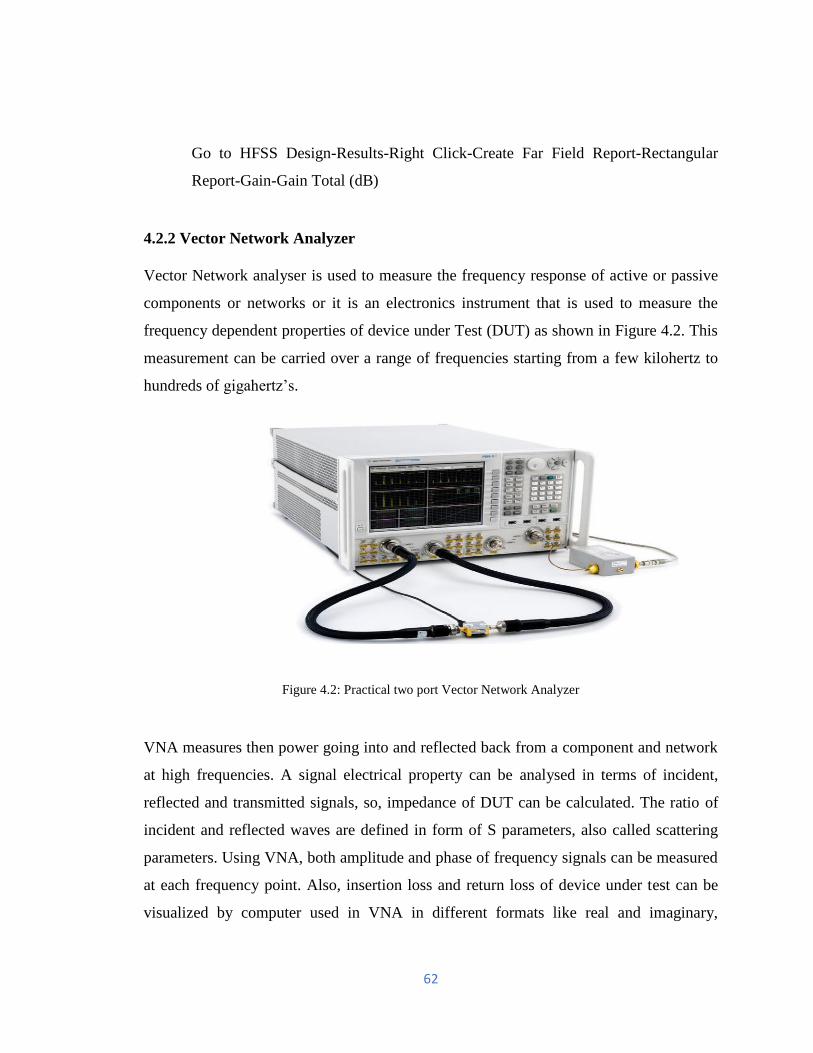
62
Go to HFSS Design-Results-Right Click-Create Far Field Report-Rectangular
Report-Gain-Gain Total (dB)
4.2.2 Vector Network Analyzer
Vector Network analyser is used to measure the frequency response of active or passive
components or networks or it is an electronics instrument that is used to measure the
frequency dependent properties of device under Test (DUT) as shown in Figure 4.2. This
measurement can be carried over a range of frequencies starting from a few kilohertz to
hundreds of gigahertz’s.
Figure 4.2: Practical two port Vector Network Analyzer
VNA measures then power going into and reflected back from a component and network
at high frequencies. A signal electrical property can be analysed in terms of incident,
reflected and transmitted signals, so, impedance of DUT can be calculated. The ratio of
incident and reflected waves are defined in form of S parameters, also called scattering
parameters. Using VNA, both amplitude and phase of frequency signals can be measured
at each frequency point. Also, insertion loss and return loss of device under test can be
visualized by computer used in VNA in different formats like real and imaginary,
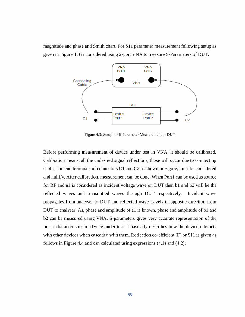
63
magnitude and phase and Smith chart. For S11 parameter measurement following setup as
given in Figure 4.3 is considered using 2-port VNA to measure S-Parameters of DUT.
Figure 4.3: Setup for S-Parameter Measurement of DUT
Before performing measurement of device under test in VNA, it should be calibrated.
Calibration means, all the undesired signal reflections, those will occur due to connecting
cables and end terminals of connectors C1 and C2 as shown in Figure, must be considered
and nullify. After calibration, measurement can be done. When Port1 can be used as source
for RF and a1 is considered as incident voltage wave on DUT than b1 and b2 will be the
reflected waves and transmitted waves through DUT respectively. Incident wave
propagates from analyser to DUT and reflected wave travels in opposite direction from
DUT to analyser. As, phase and amplitude of a1 is known, phase and amplitude of b1 and
b2 can be measured using VNA. S-parameters gives very accurate representation of the
linear characteristics of device under test, it basically describes how the device interacts
with other devices when cascaded with them. Reflection co-efficient (Γ) or S11 is given as
follows in Figure 4.4 and can calculated using expressions (4.1) and (4.2);
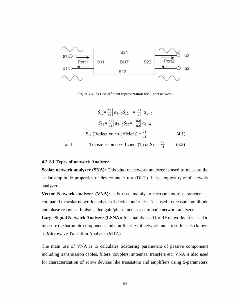
64
Figure 4.4: S11 co-efficient representation for 2-port network
𝑆11= 𝑏1
𝑎1| 𝑎2=0𝑆12 =
𝑏1
𝑎2| 𝑎1=0
𝑆21= 𝑏2
𝑎1| 𝑎2=0𝑆22=
𝑏2
𝑎2| 𝑎1=0
S11 (Reflection co-efficient) = 𝑏1
𝑎1 (4.1)
and Transmission co-efficient (T) or S21 = 𝑏2
𝑎1 (4.2)
4.2.2.1 Types of network Analyzer
Scalar network analyzer (SNA): This kind of network analyzer is used to measure the
scalar amplitude properties of device under test (DUT). It is simplest type of network
analyzer.
Vector Network analyzer (VNA): It is used mainly to measure more parameters as
compared to scalar network analyzer of device under test. It is used to measure amplitude
and phase response. It also called gain/phase meter or automatic network analyzer.
Large Signal Network Analyzer (LSNA): It is mainly used for RF networks. It is used to
measure the harmonic components and non-linarites of network under test. It is also known
as Microwave Transition Analyzer (MTA).
The main use of VNA is to calculates Scattering parameters of passive components
including transmission cables, filters, couplers, antennas, transfers etc. VNA is also used
for characterization of active devices like transistors and amplifiers using S-parameters.
65
VNA can be used in cable fault detection, in field of electromagnetic imaging to visualize
breast tumours etc.
4.2.3. Spectrum Analyzer
In field of antenna and microwave engineering, spectrum analyzer is widely used test
instrument. This test instrument, give information about signal spectrum. It measures the
amplitude of an input signal with respect to frequency as per the frequency range of the
instrument. It measures the spectrum power of known and unknown signals. Spectrum
analyzer measures electrical signal characteristics and other signals like acoustic and
optical signals spectrum can also be measured. In spectrum analyzer display, frequency is
on horizontal axis and amplitude is displayed on Vertical axis.
4.2.3.1 Types of Spectrum Analyzer: Spectrum analyzer can be of following types:
(a) Filter Bank Spectrum Analyzer
(b) Super-heterodyne Spectrum analyzer
• Filter Bank Spectrum Analyzer
Filter bank Spectrum Analyzer are also called real time spectrum analyzer. These are used
for analysing signals of Audio Frequency (AF) range and displays variations in all input
frequencies. This device, initially collects the data in Time domain form and then converts
it into the Frequency domain by using Fast Fourier Transform (FFT) method. Following
diagram shows the filter bank spectrum analyzer.
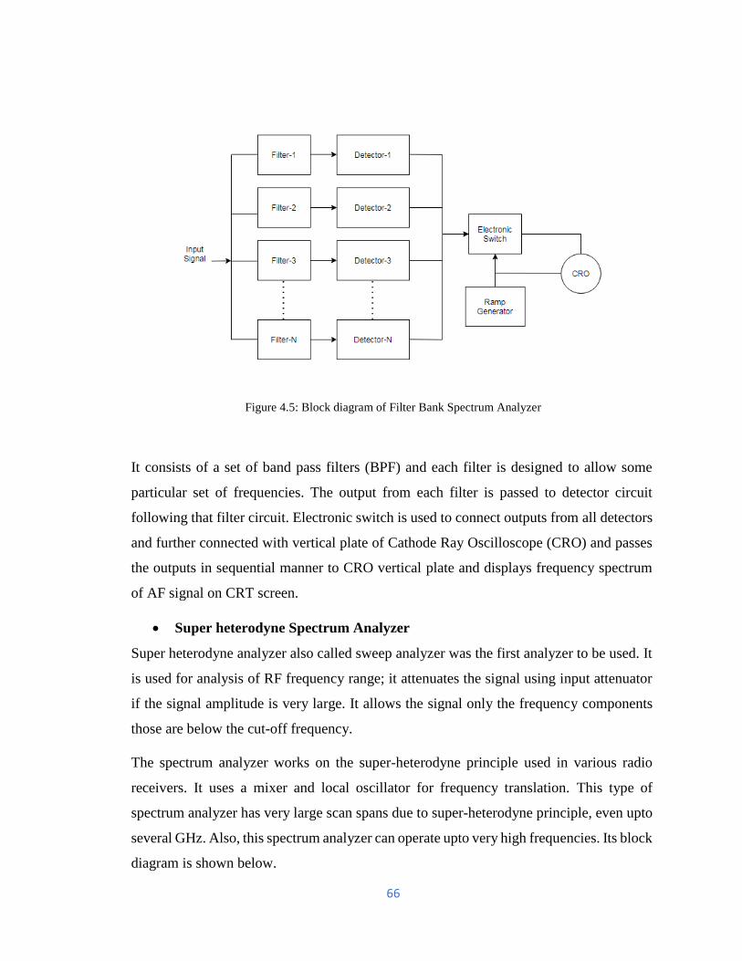
66
Figure 4.5: Block diagram of Filter Bank Spectrum Analyzer
It consists of a set of band pass filters (BPF) and each filter is designed to allow some
particular set of frequencies. The output from each filter is passed to detector circuit
following that filter circuit. Electronic switch is used to connect outputs from all detectors
and further connected with vertical plate of Cathode Ray Oscilloscope (CRO) and passes
the outputs in sequential manner to CRO vertical plate and displays frequency spectrum
of AF signal on CRT screen.
• Super heterodyne Spectrum Analyzer
Super heterodyne analyzer also called sweep analyzer was the first analyzer to be used. It
is used for analysis of RF frequency range; it attenuates the signal using input attenuator
if the signal amplitude is very large. It allows the signal only the frequency components
those are below the cut-off frequency.
The spectrum analyzer works on the super-heterodyne principle used in various radio
receivers. It uses a mixer and local oscillator for frequency translation. This type of
spectrum analyzer has very large scan spans due to super-heterodyne principle, even upto
several GHz. Also, this spectrum analyzer can operate upto very high frequencies. Its block
diagram is shown below.
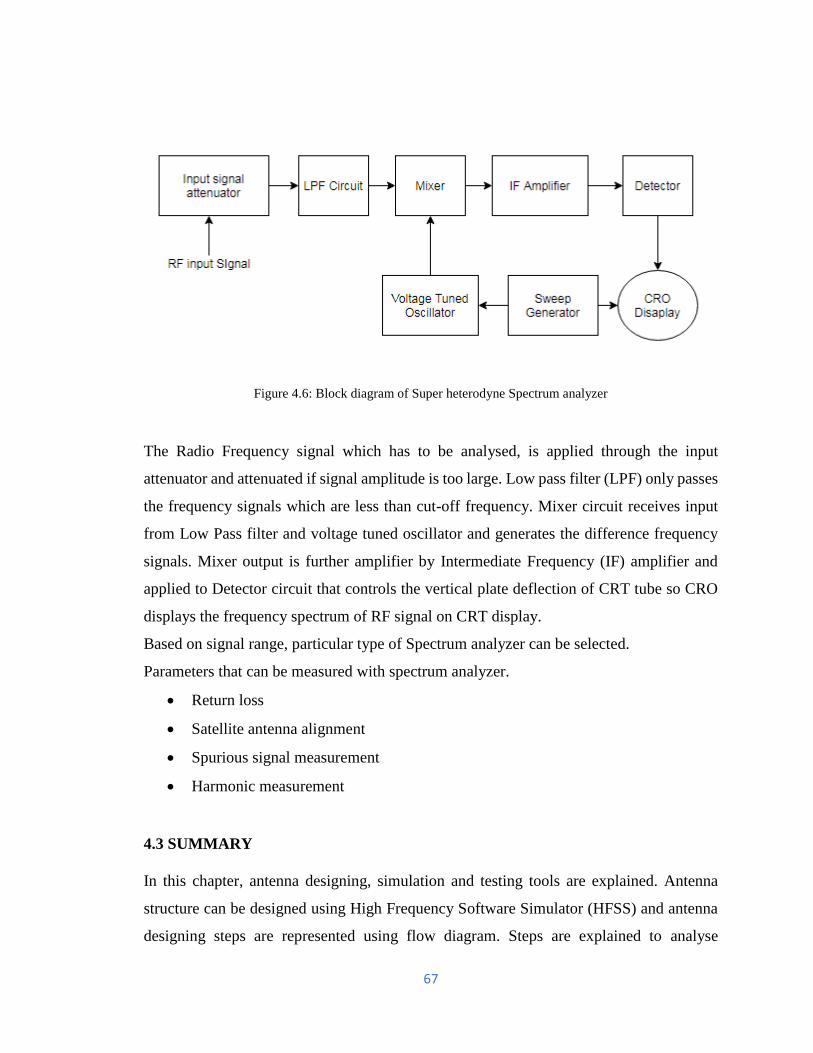
67
Figure 4.6: Block diagram of Super heterodyne Spectrum analyzer
The Radio Frequency signal which has to be analysed, is applied through the input
attenuator and attenuated if signal amplitude is too large. Low pass filter (LPF) only passes
the frequency signals which are less than cut-off frequency. Mixer circuit receives input
from Low Pass filter and voltage tuned oscillator and generates the difference frequency
signals. Mixer output is further amplifier by Intermediate Frequency (IF) amplifier and
applied to Detector circuit that controls the vertical plate deflection of CRT tube so CRO
displays the frequency spectrum of RF signal on CRT display.
Based on signal range, particular type of Spectrum analyzer can be selected.
Parameters that can be measured with spectrum analyzer.
• Return loss
• Satellite antenna alignment
• Spurious signal measurement
• Harmonic measurement
4.3 SUMMARY
In this chapter, antenna designing, simulation and testing tools are explained. Antenna
structure can be designed using High Frequency Software Simulator (HFSS) and antenna
designing steps are represented using flow diagram. Steps are explained to analyse

68
designed antenna performance in terms of return loss, gain, radiation pattern using 2-D and
3-D plots. Also, antenna testing tools are used to measure antenna return loss performance,
VSWR, gain and radiation pattern working principle, features and types are also explained
in detail.
69
CHAPTER-5
CONFIGURATION OF ANTENNA DESIGN
5.1 INTRODUCTION
In this chapter, the methodology to design Multi band Microstrip patch antenna using
Fractal and Defected structures for wireless communication applications using HFSS
Ansoft antenna simulation software is presented. For antenna designing, transmission line
design methodology is used for calculating the basic design parameters of the proposed
antenna. Proposed antenna patch dimensions, ground, and feed line dimensions are
calculated using antenna design expressions. Antenna basic patch selected is rectangular
in shape due to its easy implementation and parameter calculation as compared to circular,
semi-circular and other shapes studied in literature. For antenna designing and simulation
HFSS software is used.
Microstrip patch antenna is designed using concept of fractal geometry and defected
ground structure. To analyse antenna performance five iterations are taken into
consideration and antenna performance in calculated using antenna parameters like Gain,
Return loss (S11), VSWR etc. Initially, basic rectangular patch structure is considered and
patch dimensions are calculated using mathematical expressions. Following procedure as
give in Figure 5.1 is used for antenna designing.
5.2 FRACTAL STRUCTURES
Fractal antennas are widely used in the wireless communication. In conventional
Microstrip patch antenna to attain multi band characteristics, fractal geometry is used. To
understand the Fractal antenna, firstly we must get familiar with “What is the fractal?” It
is obtained from the Latin word ‘Fractus’ which stands for broken, fracture or irregular
fragments. It was discovered by a mathematician Benoit Mandelbrot. Fractal geometries
are had been used in field of mathematics for a century but now fractal geometries are
gaining much attention in antenna theory and microwave fields of research.
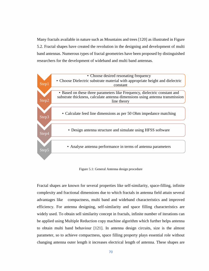
70
Many fractals available in nature such as Mountains and trees [120] as illustrated in Figure
5.2. Fractal shapes have created the revolution in the designing and development of multi
band antennas. Numerous types of fractal geometries have been proposed by distinguished
researchers for the development of wideband and multi band antennas.
Figure 5.1: General Antenna design procedure
Fractal shapes are known for several properties like self-similarity, space-filling, infinite
complexity and fractional dimensions due to which fractals in antenna field attain several
advantages like compactness, multi band and wideband characteristics and improved
efficiency. For antenna designing, self-similarity and space filling characteristics are
widely used. To obtain sell similarity concept in fractals, infinite number of iterations can
be applied using Multiple Reduction copy machine algorithm which further helps antenna
to obtain multi band behaviour [121]. In antenna design circuits, size is the almost
parameter, so to achieve compactness, space filling property plays essential role without
changing antenna outer length it increases electrical length of antenna. These shapes are
Step1
• Choose desired resonating frequency
• Choose Dielectric substrate material with appropriate height and dielectric constant
Step2
• Based on these three parameters like Frequency, dielectric constant and substrate thickness, calculate antenna dimensions using antenna transmission
line theory
Step3• Calculate feed line dimensions as per 50 Ohm impedance matching
Step4• Design antenna structure and simulate using HFSS software
Step5• Analyse antenna performance in terms of antenna parameters
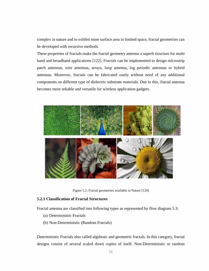
71
complex in nature and to exhibit more surface area in limited space, fractal geometries can
be developed with recursive methods.
These properties of fractals make the fractal geometry antenna a superb structure for multi
band and broadband applications [122]. Fractals can be implemented to design microstrip
patch antennas, wire antennas, arrays, loop antenna, log periodic antennas or hybrid
antennas. Moreover, fractals can be fabricated easily without need of any additional
components on different type of dielectric substrate materials. Due to this, fractal antenna
becomes more reliable and versatile for wireless application gadgets.
Figure 5.2: Fractal geometries available in Nature [120]
5.2.1 Classification of Fractal Structures
Fractal antenna are classified into following types as represented by flow diagram 5.3:
(a) Deterministic Fractals
(b) Non-Deterministic (Random Fractals)
Deterministic Fractals also called algebraic and geometric fractals. In this category, fractal
designs consist of several scaled down copies of itself. Non-Deterministic or random
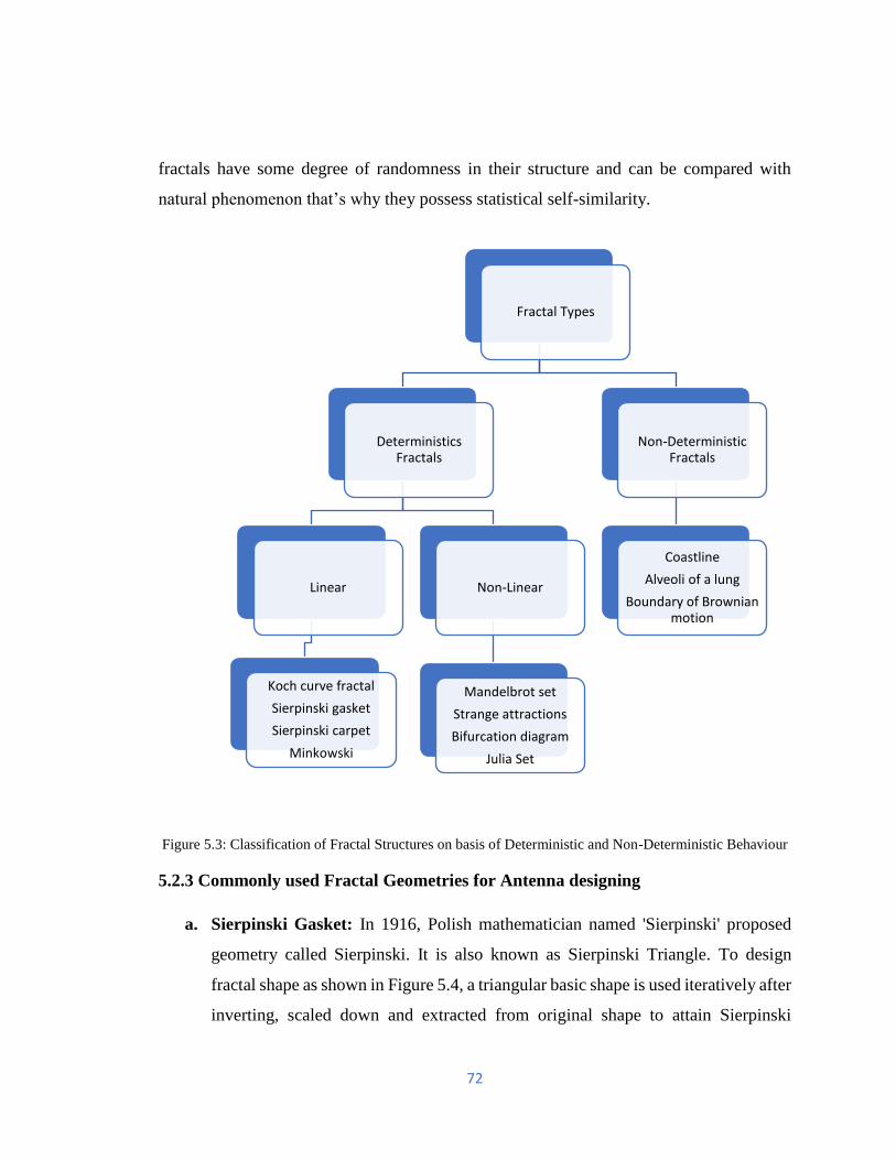
72
fractals have some degree of randomness in their structure and can be compared with
natural phenomenon that’s why they possess statistical self-similarity.
Figure 5.3: Classification of Fractal Structures on basis of Deterministic and Non-Deterministic Behaviour
5.2.3 Commonly used Fractal Geometries for Antenna designing
a. Sierpinski Gasket: In 1916, Polish mathematician named 'Sierpinski' proposed
geometry called Sierpinski. It is also known as Sierpinski Triangle. To design
fractal shape as shown in Figure 5.4, a triangular basic shape is used iteratively after
inverting, scaled down and extracted from original shape to attain Sierpinski
Fractal Types
Deterministics Fractals
Linear
Koch curve fractal
Sierpinski gasket
Sierpinski carpet
Minkowski
Non-Linear
Mandelbrot set
Strange attractions
Bifurcation diagram
Julia Set
Non-Deterministic Fractals
Coastline
Alveoli of a lung
Boundary of Brownian motion
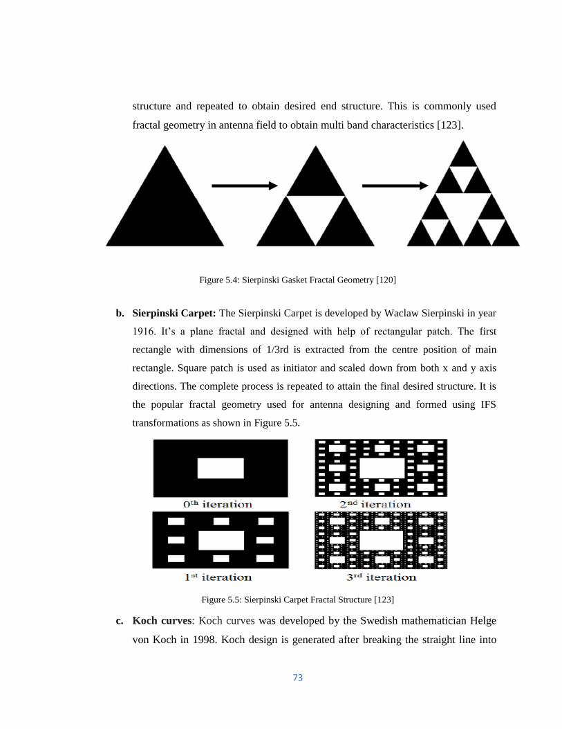
73
structure and repeated to obtain desired end structure. This is commonly used
fractal geometry in antenna field to obtain multi band characteristics [123].
Figure 5.4: Sierpinski Gasket Fractal Geometry [120]
b. Sierpinski Carpet: The Sierpinski Carpet is developed by Waclaw Sierpinski in year
1916. It’s a plane fractal and designed with help of rectangular patch. The first
rectangle with dimensions of 1/3rd is extracted from the centre position of main
rectangle. Square patch is used as initiator and scaled down from both x and y axis
directions. The complete process is repeated to attain the final desired structure. It is
the popular fractal geometry used for antenna designing and formed using IFS
transformations as shown in Figure 5.5.
Figure 5.5: Sierpinski Carpet Fractal Structure [123]
c. Koch curves: Koch curves was developed by the Swedish mathematician Helge
von Koch in 1998. Koch design is generated after breaking the straight line into
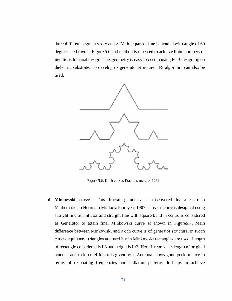
74
three different segments x, y and z. Middle part of line is bended with angle of 60
degrees as shown in Figure 5.6 and method is repeated to achieve finite numbers of
iterations for final design. This geometry is easy to design using PCB designing on
dielectric substrate. To develop its generator structure, IFS algorithm can also be
used.
Figure 5.6: Koch curves Fractal structure [123]
d. Minkowski curves: This fractal geometry is discovered by a German
Mathematician Hermann Minkowski in year 1907. This structure is designed using
straight line as Initiator and straight line with square bend in centre is considered
as Generator to attain final Minkowski curve as shown in Figure5.7. Main
difference between Minkowski and Koch curve is of generator structure, in Koch
curves equilateral triangles are used but in Minkowski rectangles are used. Length
of rectangle considered is L3 and height is Lr3. Here L represents length of original
antenna and ratio co-efficient is given by r. Antenna shows good performance in
terms of resonating frequencies and radiation patterns. It helps to achieve
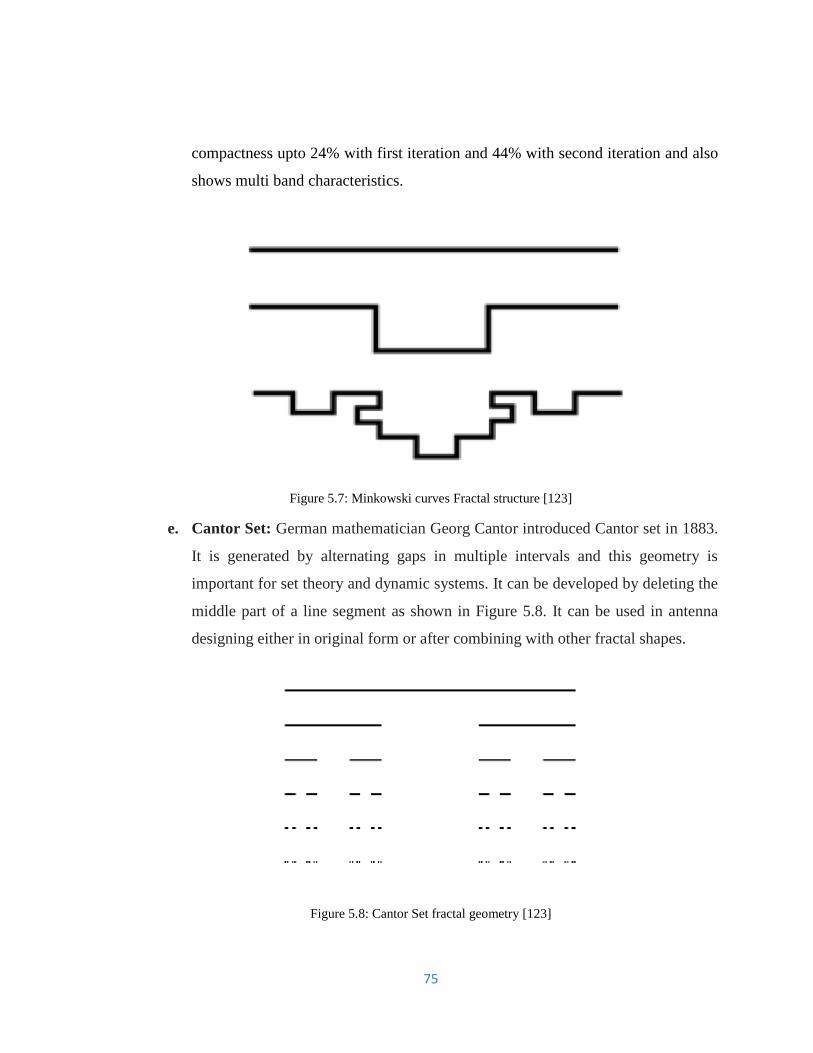
75
compactness upto 24% with first iteration and 44% with second iteration and also
shows multi band characteristics.
Figure 5.7: Minkowski curves Fractal structure [123]
e. Cantor Set: German mathematician Georg Cantor introduced Cantor set in 1883.
It is generated by alternating gaps in multiple intervals and this geometry is
important for set theory and dynamic systems. It can be developed by deleting the
middle part of a line segment as shown in Figure 5.8. It can be used in antenna
designing either in original form or after combining with other fractal shapes.
Figure 5.8: Cantor Set fractal geometry [123]
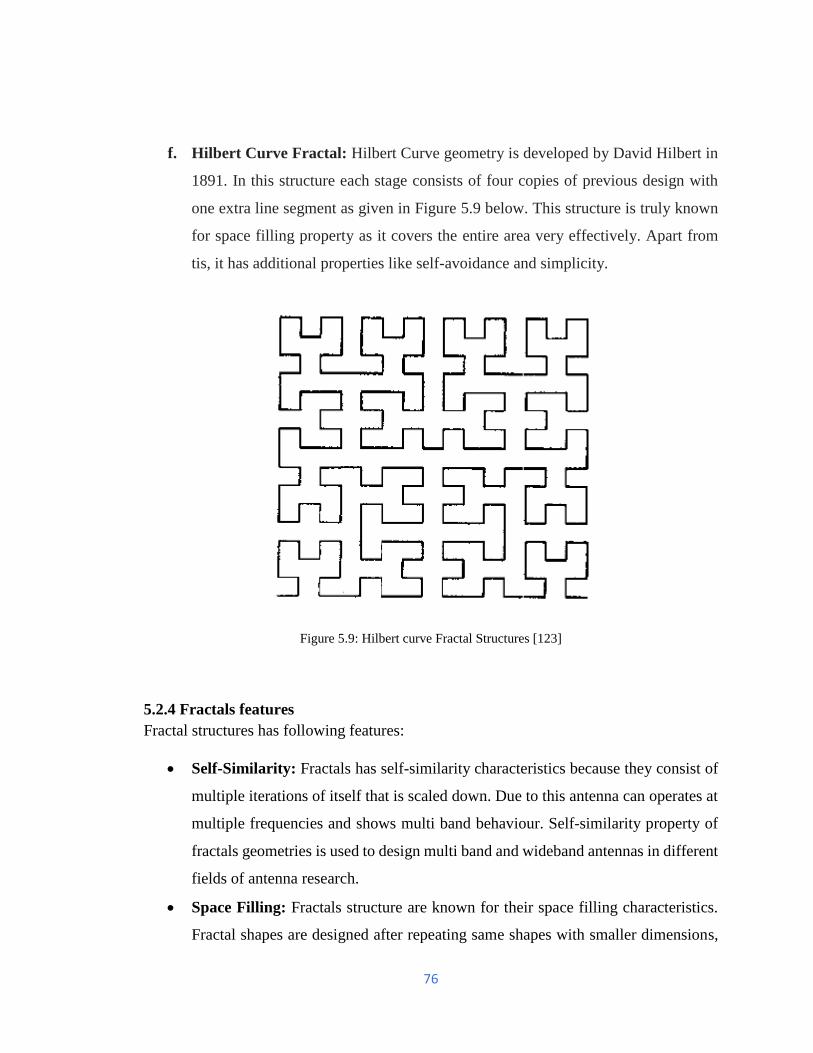
76
f. Hilbert Curve Fractal: Hilbert Curve geometry is developed by David Hilbert in
1891. In this structure each stage consists of four copies of previous design with
one extra line segment as given in Figure 5.9 below. This structure is truly known
for space filling property as it covers the entire area very effectively. Apart from
tis, it has additional properties like self-avoidance and simplicity.
Figure 5.9: Hilbert curve Fractal Structures [123]
5.2.4 Fractals features
Fractal structures has following features:
• Self-Similarity: Fractals has self-similarity characteristics because they consist of
multiple iterations of itself that is scaled down. Due to this antenna can operates at
multiple frequencies and shows multi band behaviour. Self-similarity property of
fractals geometries is used to design multi band and wideband antennas in different
fields of antenna research.
• Space Filling: Fractals structure are known for their space filling characteristics.
Fractal shapes are designed after repeating same shapes with smaller dimensions,
77
so due to this advantage of fractals they are considered as best designs to fill larges
spaces in antenna very efficiently as compared to other designs. Fractals make large
shapes to be packed into the small areas. Hence, fractal shapes are used to achieve
antenna miniaturization. Space filling properties of antenna can be used in
applications where antenna enlarge antenna lengths are needed with small
dimensions, so fractals shapes help to increase electrical length of antenna structure
without increasing overall dimensions of antenna.
• Miniaturization: To achieve compactness in design, researches find methods to
integrate long wires to assemble sin such a way that final structure should occupy
a small area [124]. Also, to obtain antenna resonance at low frequencies because
according to antenna field theory, is length of electrical conductor is more than
frequency of resonance will be lower due to rate of coupling between opposite
currents that reduces the effective overall length of total wire and results in increase
in resonance frequency.
5.2.5 Fractals Advantages and Disadvantages
The numerous positives and negatives of fractals are listed below:
Advantages
• Increase in bandwidth
• Good impedance matching
• Multi band and wideband characteristics
• Improved Voltage Standing Wave ratio
• Component matching not needed
• Provides high directivity and reduces side lobes in antenna
• Antenna can be designed using improved gain and radiation characteristics
Disadvantages
• More complexity in design
78
• Heavy calculations need to model these antennas.
• Antenna with higher iteration fractals are more difficult to fabricate.
Designing the antenna prototype is expensive and leads to errors
5.3 DEFECTED STRUCTURES
In field of microwave engineering, research discovers several techniques and theories to
design radio frequency and microwave components with improved characteristics. One
technique that is seeking much attention now is Defected Ground Structures (DGS). Slots
and defects etched upon ground plane of microwave components are called Defected
Ground structures. It is opted method to enhance antenna parameters like operating
bandwidth, gain, cross-polarization etc. DGS can be configurations of periodic and non-
periodic structures in ground plan used to divert the current distribution which actually
changes the reactive characteristics of the circuit like inductance and capacitance. In
literature, various defected structures have been discovered and used like square, spiral,
dumbbell, L-shaped, rectangular, circular, U-shaped, hexagonal, V-shaped, concentric,
arrow head etc. [125-128]. Current distribution and propagation through ground plane can
be controlled by properly selecting dimensions and shapes of defected structures which
further controls elect magnetic waves generation and transmission through substrate
material. Also, due to changes in inductive and capacitive properties of ground plane,
additional frequency bands can be achieved which leads to multi band behaviour of circuits
and very useful in wireless communication devices. The first DGS structures was
discovered by Park et al. [124] as a dumbbell-shaped cells and Guha et al. [130] explains
different patterns of DGS like fractal, half circle, split ring, spiral, V-Shaped etc.
These structures basically give more flexibility to microwave circuits designing and paved
the way towards extensive range of applications. In yesteryears, many microwave circuits
and milli-meter devices have designed to minimize the spurious harmonics, also to reduce
dimensions of circuits with DGS. Various DGS printed on ground plan reported in
literature are given below in Figure 5.10.
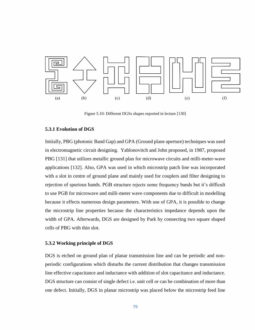
79
Figure 5.10: Different DGSs shapes reported in lecture [130]
5.3.1 Evolution of DGS
Initially, PBG (photonic Band Gap) and GPA (Ground plane aperture) techniques was used
in electromagnetic circuit designing. Yablonovitch and John proposed, in 1987, proposed
PBG [131] that utilizes metallic ground plan for microwave circuits and milli-meter-wave
applications [132]. Also, GPA was used in which microstrip patch line was incorporated
with a slot in centre of ground plane and mainly used for couplers and filter designing to
rejection of spurious bands. PGB structure rejects some frequency bands but it’s difficult
to use PGB for microwave and milli-meter wave components due to difficult in modelling
because it effects numerous design parameters. With use of GPA, it is possible to change
the microstrip line properties because the characteristics impedance depends upon the
width of GPA. Afterwards, DGS are designed by Park by connecting two square shaped
cells of PBG with thin slot.
5.3.2 Working principle of DGS
DGS is etched on ground plan of planar transmission line and can be periodic and non-
periodic configurations which disturbs the current distribution that changes transmission
line effective capacitance and inductance with addition of slot capacitance and inductance.
DGS structure can consist of single defect i.e. unit cell or can be combination of more than
one defect. Initially, DGS in planar microstrip was placed below the microstrip feed line
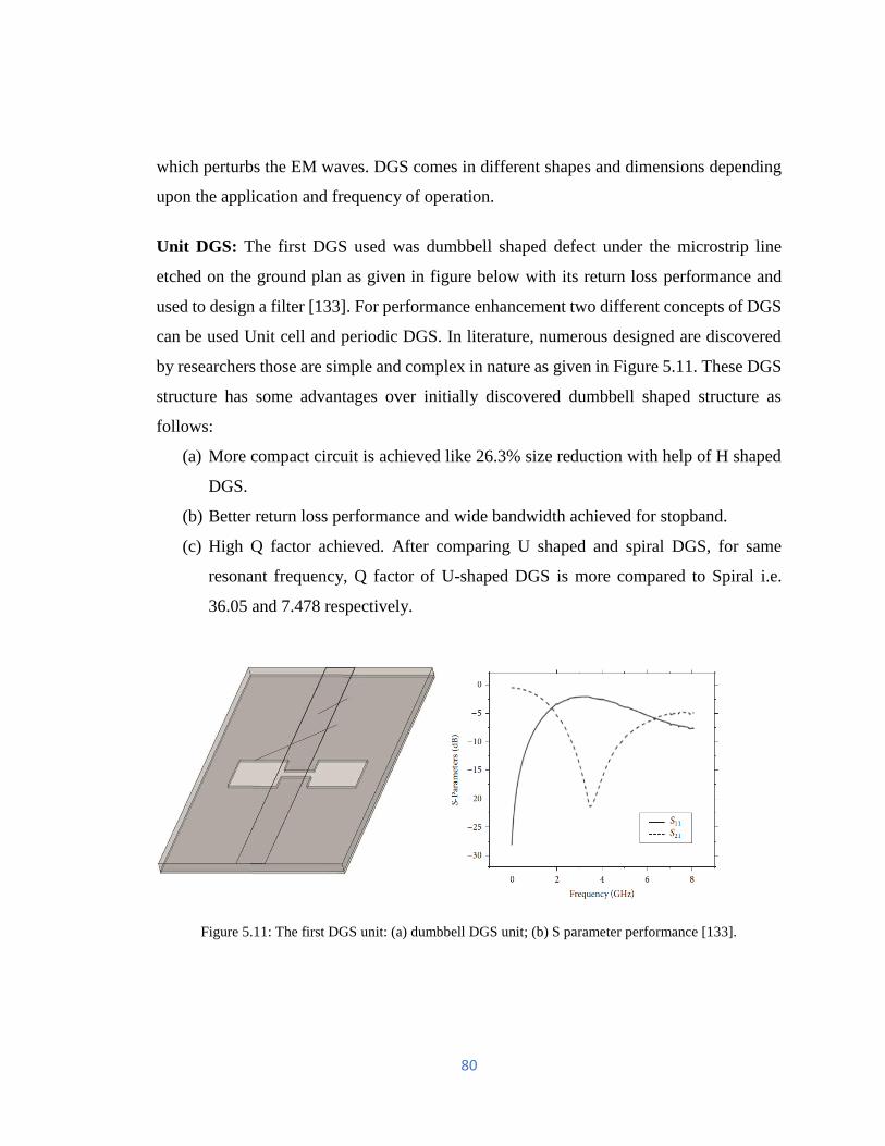
80
which perturbs the EM waves. DGS comes in different shapes and dimensions depending
upon the application and frequency of operation.
Unit DGS: The first DGS used was dumbbell shaped defect under the microstrip line
etched on the ground plan as given in figure below with its return loss performance and
used to design a filter [133]. For performance enhancement two different concepts of DGS
can be used Unit cell and periodic DGS. In literature, numerous designed are discovered
by researchers those are simple and complex in nature as given in Figure 5.11. These DGS
structure has some advantages over initially discovered dumbbell shaped structure as
follows:
(a) More compact circuit is achieved like 26.3% size reduction with help of H shaped
DGS.
(b) Better return loss performance and wide bandwidth achieved for stopband.
(c) High Q factor achieved. After comparing U shaped and spiral DGS, for same
resonant frequency, Q factor of U-shaped DGS is more compared to Spiral i.e.
36.05 and 7.478 respectively.
Figure 5.11: The first DGS unit: (a) dumbbell DGS unit; (b) S parameter performance [133].
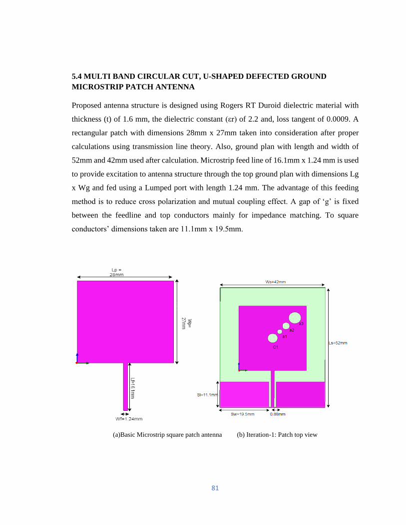
81
5.4 MULTI BAND CIRCULAR CUT, U-SHAPED DEFECTED GROUND
MICROSTRIP PATCH ANTENNA
Proposed antenna structure is designed using Rogers RT Duroid dielectric material with
thickness (t) of 1.6 mm, the dielectric constant (εr) of 2.2 and, loss tangent of 0.0009. A
rectangular patch with dimensions 28mm x 27mm taken into consideration after proper
calculations using transmission line theory. Also, ground plan with length and width of
52mm and 42mm used after calculation. Microstrip feed line of 16.1mm x 1.24 mm is used
to provide excitation to antenna structure through the top ground plan with dimensions Lg
x Wg and fed using a Lumped port with length 1.24 mm. The advantage of this feeding
method is to reduce cross polarization and mutual coupling effect. A gap of ‘g’ is fixed
between the feedline and top conductors mainly for impedance matching. To square
conductors’ dimensions taken are 11.1mm x 19.5mm.
(a)Basic Microstrip square patch antenna (b) Iteration-1: Patch top view
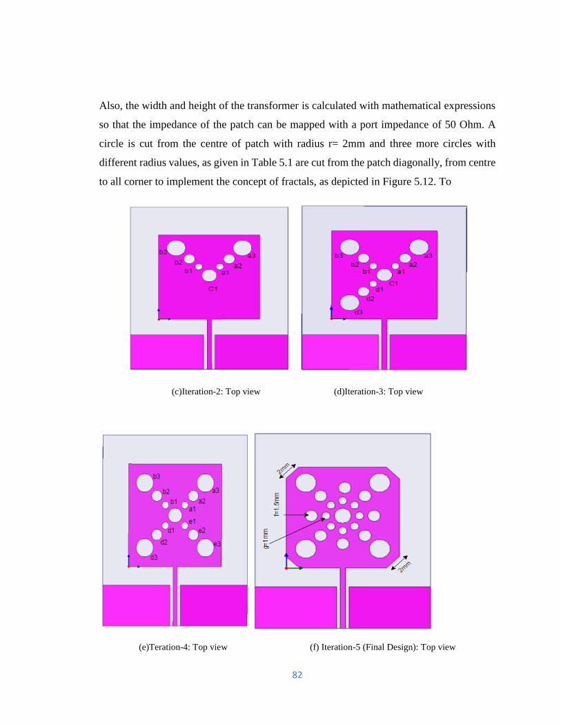
82
Also, the width and height of the transformer is calculated with mathematical expressions
so that the impedance of the patch can be mapped with a port impedance of 50 Ohm. A
circle is cut from the centre of patch with radius r= 2mm and three more circles with
different radius values, as given in Table 5.1 are cut from the patch diagonally, from centre
to all corner to implement the concept of fractals, as depicted in Figure 5.12. To
(c)Iteration-2: Top view (d)Iteration-3: Top view
(e)Teration-4: Top view (f) Iteration-5 (Final Design): Top view
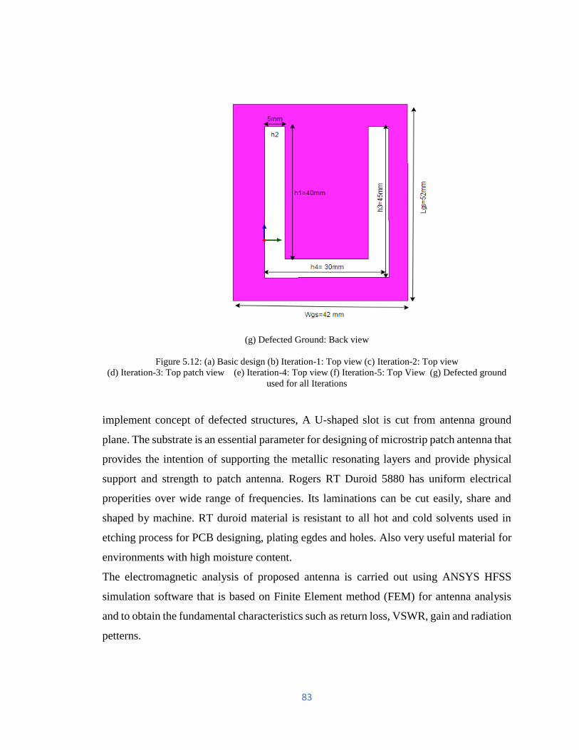
83
(g) Defected Ground: Back view
Figure 5.12: (a) Basic design (b) Iteration-1: Top view (c) Iteration-2: Top view
(d) Iteration-3: Top patch view (e) Iteration-4: Top view (f) Iteration-5: Top View (g) Defected ground
used for all Iterations
implement concept of defected structures, A U-shaped slot is cut from antenna ground
plane. The substrate is an essential parameter for designing of microstrip patch antenna that
provides the intention of supporting the metallic resonating layers and provide physical
support and strength to patch antenna. Rogers RT Duroid 5880 has uniform electrical
properities over wide range of frequencies. Its laminations can be cut easily, share and
shaped by machine. RT duroid material is resistant to all hot and cold solvents used in
etching process for PCB designing, plating egdes and holes. Also very useful material for
environments with high moisture content.
The electromagnetic analysis of proposed antenna is carried out using ANSYS HFSS
simulation software that is based on Finite Element method (FEM) for antenna analysis
and to obtain the fundamental characteristics such as return loss, VSWR, gain and radiation
petterns.
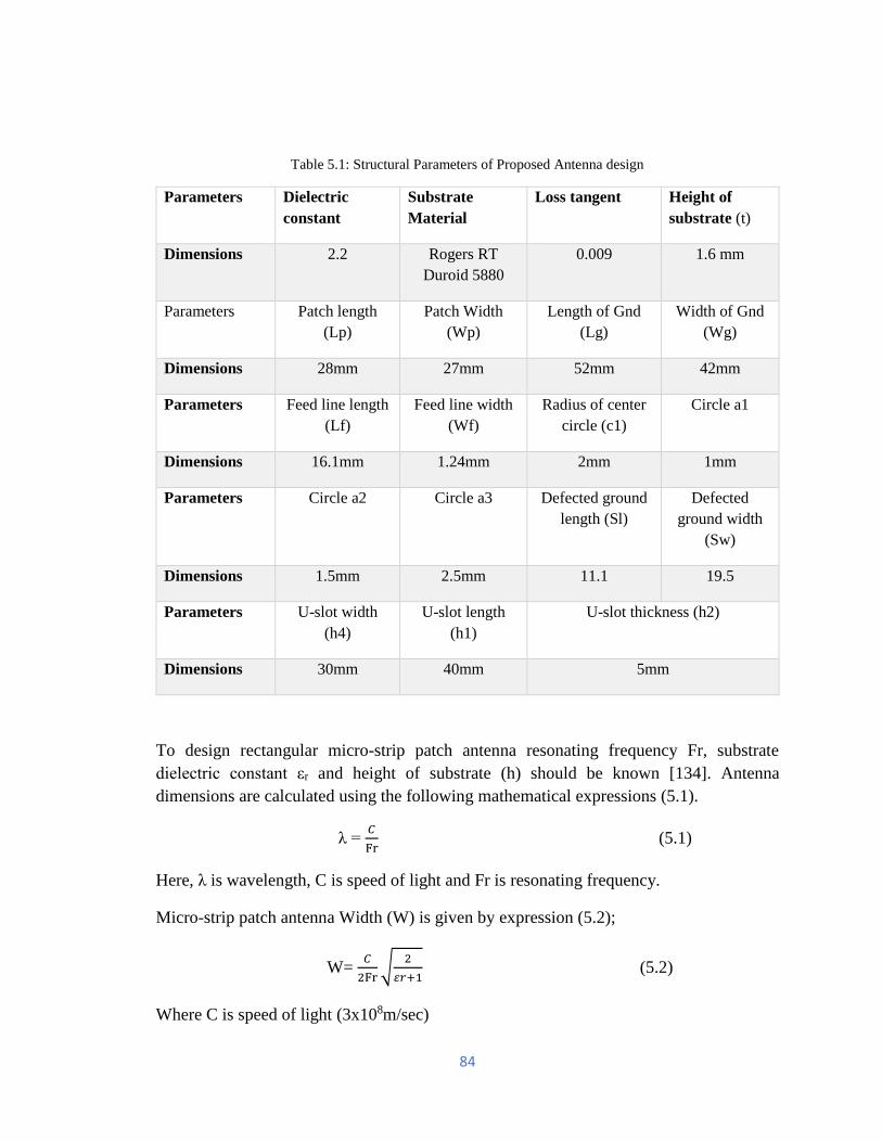
84
Table 5.1: Structural Parameters of Proposed Antenna design
Parameters Dielectric
constant
Substrate
Material
Loss tangent Height of
substrate (t)
Dimensions 2.2 Rogers RT
Duroid 5880
0.009 1.6 mm
Parameters Patch length
(Lp)
Patch Width
(Wp)
Length of Gnd
(Lg)
Width of Gnd
(Wg)
Dimensions 28mm 27mm 52mm 42mm
Parameters Feed line length
(Lf)
Feed line width
(Wf)
Radius of center
circle (c1)
Circle a1
Dimensions 16.1mm 1.24mm 2mm 1mm
Parameters Circle a2 Circle a3 Defected ground
length (Sl)
Defected
ground width
(Sw)
Dimensions 1.5mm 2.5mm 11.1 19.5
Parameters U-slot width
(h4)
U-slot length
(h1)
U-slot thickness (h2)
Dimensions 30mm 40mm 5mm
To design rectangular micro-strip patch antenna resonating frequency Fr, substrate
dielectric constant εr and height of substrate (h) should be known [134]. Antenna
dimensions are calculated using the following mathematical expressions (5.1).
λ = 𝐶
Fr (5.1)
Here, λ is wavelength, C is speed of light and Fr is resonating frequency.
Micro-strip patch antenna Width (W) is given by expression (5.2);
W= 𝐶
2Fr√
2
𝜀𝑟+1 (5.2)
Where C is speed of light (3x10⁸m/sec)
85
Effective dielectric constant of the substrate is calculated using expression (5.3):
εreff= 𝜀𝑟+1
2+
𝜀𝑟−1
2(1+12
ℎ
𝑤)−1
2 (5.3)
Here ‘h’ is the thickness or height of the substrate and ‘W’ is the width of the antenna.
Effective length of the antenna at resonant frequency is calculated as given in expression
(5.4);
𝐿𝑒𝑓𝑓= 𝐶
2𝐹𝑟√𝜀𝑟𝑒𝑓𝑓 (5.4)
Antenna length extension is calculated with expression (5.5);
ΔL = 0.412h[𝜀𝑟𝑒𝑓𝑓+0.3
𝜀𝑟𝑒𝑓𝑓−0.258
𝑊
ℎ+0.264
𝑊
ℎ+0.8
] (5.5)
Total length of antenna is calculated using expression (5.6);
L= Leff-2ΔL (5.6)
Substrate width and length is calculated as given in expression (5.7);
Lg=L+6h and Wg=W+6h (5.7)
Height of substrate is given in expression (5.8);
h= 0.0606𝜆
√∈𝑟 (5.8)
Feed line dimensions are calculated using expression (5.9):
Lf = 𝜆𝑔
4
λg = 𝜆
√𝜀𝑒𝑓𝑓 (5.9)
Radiation box dimensions can be calculated using expression (5.10);
Axis position= −𝜆𝑔
6+
−𝜆𝑔
6+
−𝜆𝑔
6
Length = −𝜆𝑔
6+
−𝜆𝑔
6+ 𝐿𝑔
Width = −𝜆𝑔
6+
−𝜆𝑔
6+ 𝑊𝑔
86
Height= −𝜆𝑔
6+
−𝜆𝑔
6+ ℎg (5.10)
By implementing the concept of fractals and defected in antenna designing, for every
iteration performance of antenna design is observed in terms of S11 parameters, gain,
bandwidth and operating frequency. Fractal geometry gives antenna design more
compactness due to its self-similarity property. Also, impedance matching is better of
antenna structure with antenna feedline, so that maximum signal energy is converted form
voltage and current signals into electromagnetic waves. This further enhances the antenna
gain and bandwidth performance, maximum gain achieved is 9.16 dB for designed antenna.
In proposed antenna designing, concept of DGS is used to further improve antenna
performance in terms of antenna gain and bandwidth. DGS are the shaped, those are etched
on the plane ground of antenna structure. It is opted method in antenna and microwave
engineering to enhance antenna parameters like operating bandwidth, gain, cross-
polarization etc. In proposed antenna, U-shaped DGS is considered and used to divert the
current distribution which actually changes the reactive characteristics of the circuit like
inductance and capacitance. The effect of U-shaped defected structure is analysed with all
iterations with length and width of 20mm x 40mm and inner gap of 5mm as given in Table
5.1 and shown in Figure 5.12(g).
5.5 ANTENNA SIMULATED RESULTS
Proposed antenna results are calculated in terms of return loss (S11), VSWR, gain for all
Iterations using HFSS simulation tool from 1GHz to 15GHz. Antenna performance is
analysed and compared after thoroughly comparing the effect of all iterations of proposed
antenna.
Reflection coefficient is defined as ratio 0
0
in
in
Z Z
Z Z
− =
+.Where inZ is input impedance of the
antenna and 0Z is the impedance of transmission lines. A typical value of reflection
coefficient lies in between 0 1 . Figure 5.13(a), shows the return vs frequency plot of
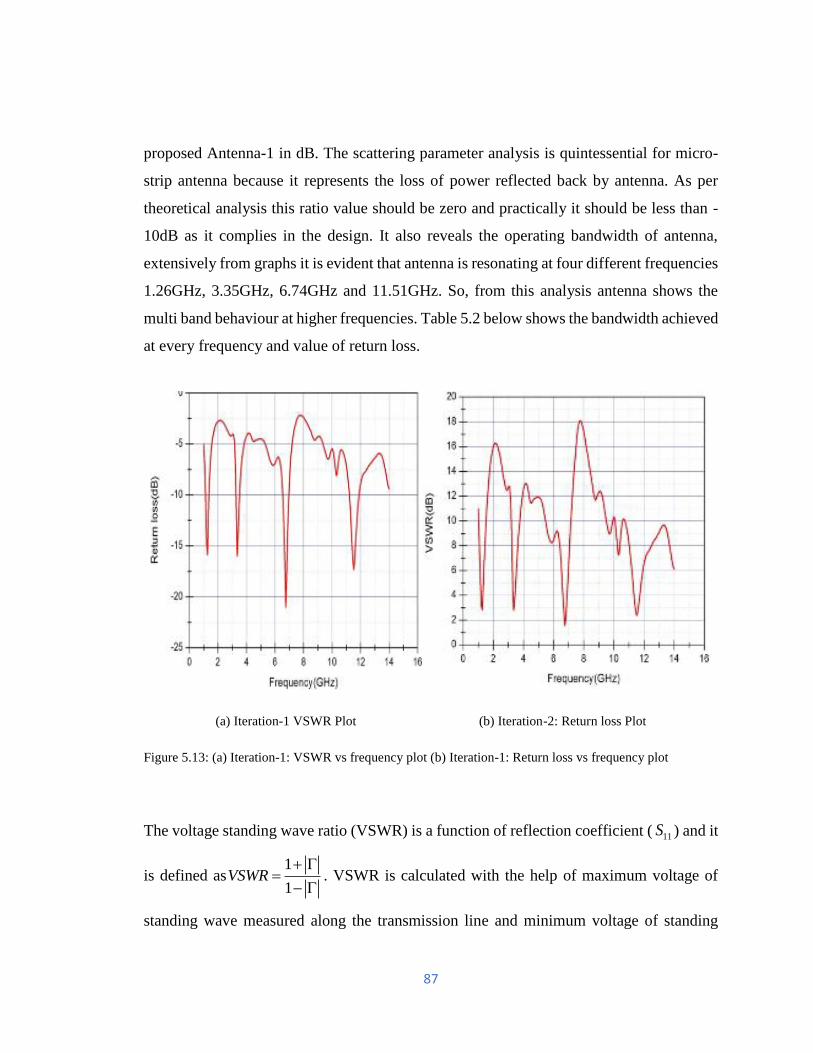
87
proposed Antenna-1 in dB. The scattering parameter analysis is quintessential for micro-
strip antenna because it represents the loss of power reflected back by antenna. As per
theoretical analysis this ratio value should be zero and practically it should be less than -
10dB as it complies in the design. It also reveals the operating bandwidth of antenna,
extensively from graphs it is evident that antenna is resonating at four different frequencies
1.26GHz, 3.35GHz, 6.74GHz and 11.51GHz. So, from this analysis antenna shows the
multi band behaviour at higher frequencies. Table 5.2 below shows the bandwidth achieved
at every frequency and value of return loss.
(a) Iteration-1 VSWR Plot (b) Iteration-2: Return loss Plot
Figure 5.13: (a) Iteration-1: VSWR vs frequency plot (b) Iteration-1: Return loss vs frequency plot
The voltage standing wave ratio (VSWR) is a function of reflection coefficient ( 11S ) and it
is defined as1
1VSWR
+ =
− . VSWR is calculated with the help of maximum voltage of
standing wave measured along the transmission line and minimum voltage of standing
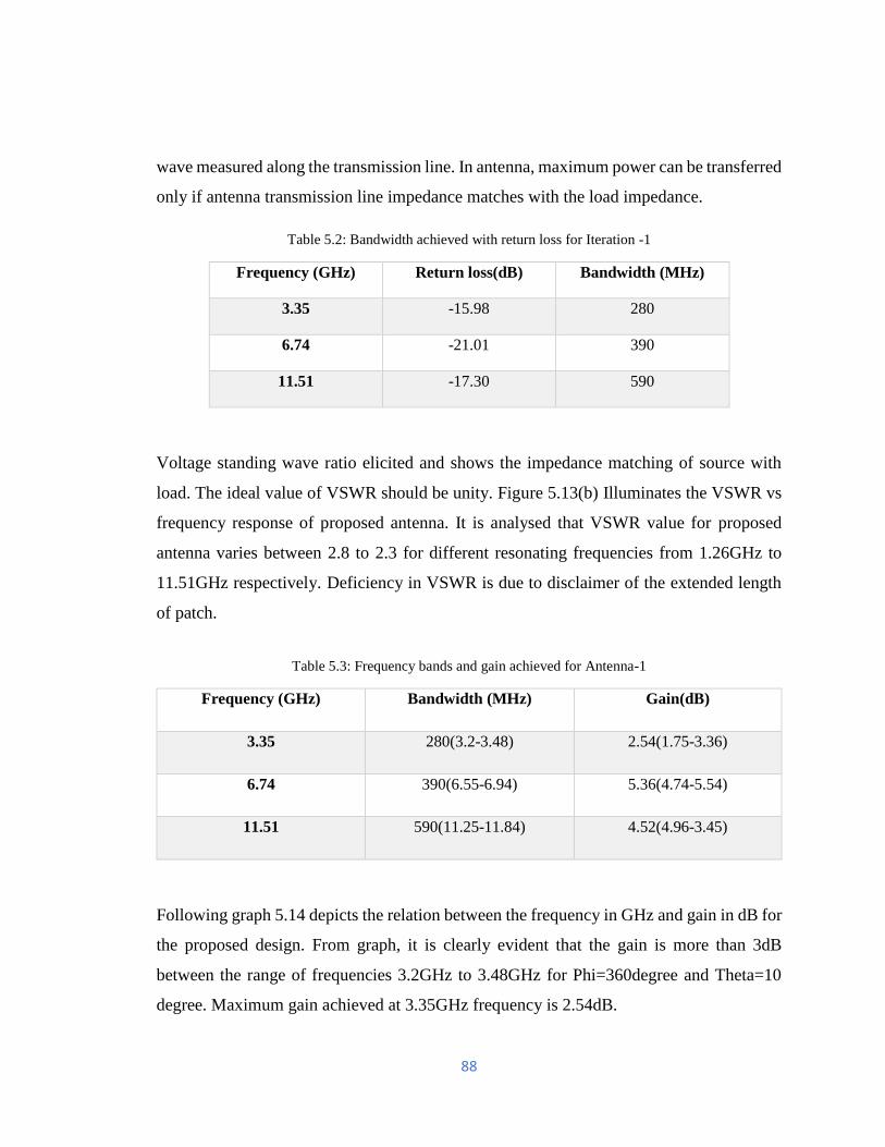
88
wave measured along the transmission line. In antenna, maximum power can be transferred
only if antenna transmission line impedance matches with the load impedance.
Table 5.2: Bandwidth achieved with return loss for Iteration -1
Frequency (GHz) Return loss(dB) Bandwidth (MHz)
3.35 -15.98 280
6.74 -21.01 390
11.51 -17.30 590
Voltage standing wave ratio elicited and shows the impedance matching of source with
load. The ideal value of VSWR should be unity. Figure 5.13(b) Illuminates the VSWR vs
frequency response of proposed antenna. It is analysed that VSWR value for proposed
antenna varies between 2.8 to 2.3 for different resonating frequencies from 1.26GHz to
11.51GHz respectively. Deficiency in VSWR is due to disclaimer of the extended length
of patch.
Table 5.3: Frequency bands and gain achieved for Antenna-1
Frequency (GHz) Bandwidth (MHz) Gain(dB)
3.35 280(3.2-3.48) 2.54(1.75-3.36)
6.74 390(6.55-6.94) 5.36(4.74-5.54)
11.51 590(11.25-11.84) 4.52(4.96-3.45)
Following graph 5.14 depicts the relation between the frequency in GHz and gain in dB for
the proposed design. From graph, it is clearly evident that the gain is more than 3dB
between the range of frequencies 3.2GHz to 3.48GHz for Phi=360degree and Theta=10
degree. Maximum gain achieved at 3.35GHz frequency is 2.54dB.
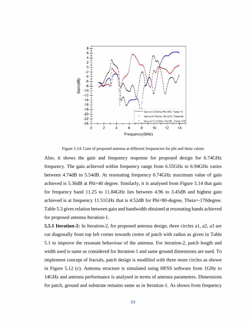
89
Figure 5.14: Gain of proposed antenna at different frequencies for phi and theta values
Also, it shows the gain and frequency response for proposed design for 6.74GHz
frequency. The gain achieved within frequency range from 6.55GHz to 6.94GHz varies
between 4.74dB to 5.54dB. At resonating frequency 6.74GHz maximum value of gain
achieved is 5.36dB at Phi=40 degree. Similarly, it is analysed from Figure 5.14 that gain
for frequency band 11.25 to 11.84GHz lies between 4.96 to 3.45dB and highest gain
achieved is at frequency 11.51GHz that is 4.52dB for Phi=80-degree, Theta=-170degree.
Table 5.3 gives relation between gain and bandwidth obtained at resonating bands achieved
for proposed antenna Iteration-1.
5.5.1 Iteration-2: In Iteration-2, for proposed antenna design, three circles a1, a2, a3 are
cut diagonally from top left corner towards centre of patch with radius as given in Table
5.1 to improve the resonant behaviour of the antenna. For iteration-2, patch length and
width used is same as considered for Iteration-1 and same ground dimensions are used. To
implement concept of fractals, patch design is modified with three more circles as shown
in Figure 5.12 (c). Antenna structure is simulated using HFSS software from 1GHz to
14GHz and antenna performance is analysed in terms of antenna parameters. Dimensions
for patch, ground and substrate remains same as in Iteration-1. As shown from frequency
90
vs return loss graph in Figure 5.15(a), proposed antenna is resonating at five frequencies
3.67, 6.16, 7.07, 10.47 and 11.64GHz. Table 5.4 shows the bandwidth range of proposed
antenna for these resonating frequencies. The wide bandwidth is achieved at resonating
frequency 11.97 i.e. 520MHz as per requirement for 5G applications.
(a) Iteration-2: Return loss plot (b) Iteration-2: VSWR plot
Figure 5.15: (a) Iteration-2: Return loss (S11) v/s frequency response (b)Iteration-2: VSWR vs frequency
plot
Table 5.4: Bandwidth achieved with return loss for Iteration-2
VSWR vs frequency response for Iteration-2 is presented in Figure 5.15 (b). The theoretical
value of VSWR should be unity. It is analysed that VSWR value for proposed antenna
varies from 0.48 to 2.15 for resonating frequencies between 3.67 to 11.64GHz respectively.
The best value achieved is at resonating frequency 3.67 i.e. 0.48.
Frequency (GHz) Return loss(dB) Bandwidth (MHz)
3.67 -31.16 480
6.16 -12.97 3960
7.07 -17.08 2440
10.47 -15.68 2880
11.64 -18.15 2150
91
As it is stated from theoretical concept that gain should be more than 3dB. For Iteration-2,
it is analysed from graph in Figure 5.16, which gain of antenna varies between 5.3dB to
5.49dB for resonating bandwidth between 3.54GHz to 3.80GHz. For resonating frequency
3.67GHz, gain achieved is 5.47dB for Phi=130-degree, Theta=20degree. The value of gain
for antenna bandwidth 6.03GHz to 6.94GHz is from 4.17 to 7.14dB as depicted from
Figure 5.16 and Table 5.5. At resonating frequency 6.16GHz value of gain is 4.3dB.
Table 5.5: Value of gain for different resonating frequency bands along with bandwidth for Iteration-2
Frequency (GHz) Bandwidth (MHz) Gain(dB)
3.67(3.54-3.80) 480 5.47(5.53-5.49)
6.16(6.03-6.94) 3960 4.3(4.17-7.14)
7.07(7.01-7.14) 2440 8.62(7.01-8.57)
10.47(10.53-10.40) 2880 6.16(5.12-6.66)
11.64(11.45-11.97) 2150 7.48(6.98-7.35)
92
Figure 5.16: Iteration-2 gain at different frequencies
Also, as shown in Figure 5.16, for resonating frequency range between 7.01GHz to
7.14GHz, gain ranges between 7.01dB to 8.57dBfor Phi=280 degree and Theta=30degree.
Value of antenna gain varies from 5.12dB to 66dB for resonating band 10.40GHz to
10.53GHz for Phi=180 degree and Theta=20degree. Similarly, gain ranges from 6.98dB to
7.35dB for frequency range from 11.45GHz to 11.97GHz respectively. It is analysed that
maximum gain for proposed antenna is achieved on two resonant bands i.e. 7.07GHz and
11.64GHz, as values of gain for these frequencies are 8.62dB and 7.48dB respectively as
shown in Table 5.5.
5.5.2 Iteration-3: Proposed antenna patch design for Iteration-3 is shown in Figure 5.12
(d). Antenna resonates at three operating frequencies 3.67, 6.74 and 11.64GHz with S11
values -24.27, -23.16 and -24.54 respectively as given in Table 5.6 below.
Table 5.6: Gain, S11 and bandwidth performance of Iteration-3
Frequency
(GHz)
S11
(dB)
BW
(MHz)
Gain
(dB)
Phi
(degree)
Theta
(degree)
VSWR
3.67 -24.27 330(3.54-
3.87)
5.27(5.4-
4.95)
150 30 1.06
6.74 -23.16 460(6.48-
6.94)
6.74(8.23-
8.02)
280 30 1.20
11.64 -24.54 390(11.45-
11.84)
7.40(7.02-
7.13)
260 140 1.03
93
(a) Iteration-3: Return loss (b) Itertaion-3: VSWR Plot
Figure 5.17: (a) S11 v/s Frequency performance for Iteration-3 (b) VSWR vs Frequency plot of Iteration-3
Figure 5.18: Gain at different frequency with phi and theta values for Iteration-3
5.5.3 Iteration-4: Patch design for proposed antenna in iteration-4 is as shown in Figure
5.12 (e). For Iteration-4 antenna designing, patch and ground dimension considered are
94
same with dielectric substrate RT Duroid with thickness 1.6mm and dielectric constant of
2.2. Proposed structure return loss performance is as given in Figure 5.19 (a), it is depicted
from graph that proposed structure resonates on three frequencies 3.67GHz, 6.68GHz, and
11.58GHz with S11 values -23.38, -21.03 and -31.72dB respectively. It is analysed from
S11 plot that antenna shows multi band behaviour. Antenna VSWR plot is given in Figure
5.19 (b) and it is depicted that for operating band achieved for proposed antenna, VSWR
performance is acceptable, as VSWR value achieved is 1.17, 1.54 and 0.45 for 3.67GHz,
6.68GHz and 11.58GHz respectively. Figure 5.20, shows simulated gain achieved for
resonating frequency bands for different values of Phi and Theta. Peak value of gain
achieved at 3.67GHz resonating frequency is 4.99 dB and it varies between 4.98 to 4.93dB
for frequency band of operation 3.61GHz to 3.80 GHz. Maximum gain achieved is at
6.68dB i.e. 7.9dB and gain variation observed for this frequency band of operation is 4.07
to 7.79dB for frequency range 6.03GHz to 6.87GHz. For proposed antenna, gain value
achieved at high frequency band 11.58GHz is 6.57dB with variations from 6.15 to 6.41dB
for frequency band 11.38 to 11.84 GHz as shown in Table 5.7 for Phi 270 and theta 140
degree. For iteration-4, impedance bandwidth obtained is 190, 840 and 460 MHz for
operating bands 3.67GHz, 6.68GHz and 11.58GHz respectively.
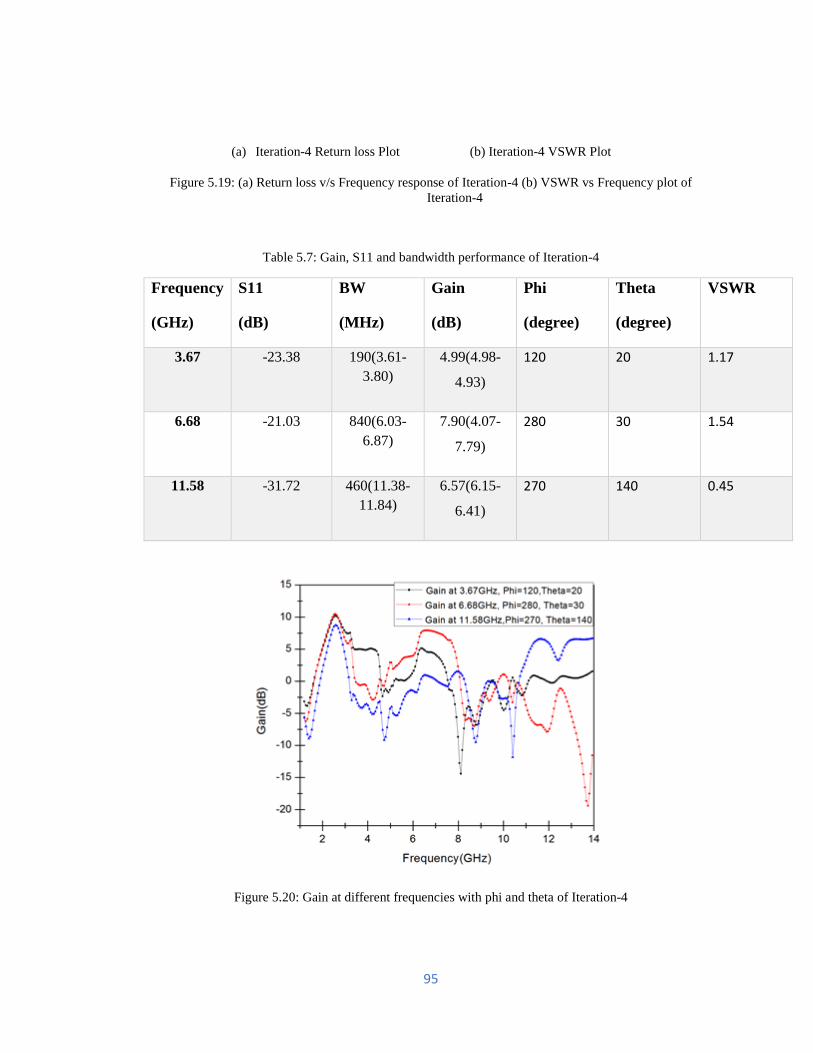
95
(a) Iteration-4 Return loss Plot (b) Iteration-4 VSWR Plot
Figure 5.19: (a) Return loss v/s Frequency response of Iteration-4 (b) VSWR vs Frequency plot of
Iteration-4
Table 5.7: Gain, S11 and bandwidth performance of Iteration-4
Frequency
(GHz)
S11
(dB)
BW
(MHz)
Gain
(dB)
Phi
(degree)
Theta
(degree)
VSWR
3.67 -23.38 190(3.61-
3.80)
4.99(4.98-
4.93)
120 20 1.17
6.68 -21.03 840(6.03-
6.87)
7.90(4.07-
7.79)
280 30 1.54
11.58 -31.72 460(11.38-
11.84)
6.57(6.15-
6.41)
270 140 0.45
Figure 5.20: Gain at different frequencies with phi and theta of Iteration-4
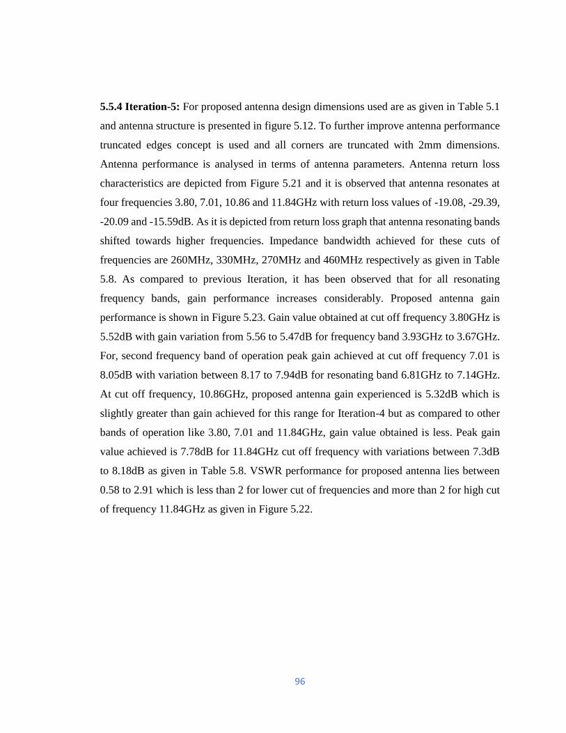
96
5.5.4 Iteration-5: For proposed antenna design dimensions used are as given in Table 5.1
and antenna structure is presented in figure 5.12. To further improve antenna performance
truncated edges concept is used and all corners are truncated with 2mm dimensions.
Antenna performance is analysed in terms of antenna parameters. Antenna return loss
characteristics are depicted from Figure 5.21 and it is observed that antenna resonates at
four frequencies 3.80, 7.01, 10.86 and 11.84GHz with return loss values of -19.08, -29.39,
-20.09 and -15.59dB. As it is depicted from return loss graph that antenna resonating bands
shifted towards higher frequencies. Impedance bandwidth achieved for these cuts of
frequencies are 260MHz, 330MHz, 270MHz and 460MHz respectively as given in Table
5.8. As compared to previous Iteration, it has been observed that for all resonating
frequency bands, gain performance increases considerably. Proposed antenna gain
performance is shown in Figure 5.23. Gain value obtained at cut off frequency 3.80GHz is
5.52dB with gain variation from 5.56 to 5.47dB for frequency band 3.93GHz to 3.67GHz.
For, second frequency band of operation peak gain achieved at cut off frequency 7.01 is
8.05dB with variation between 8.17 to 7.94dB for resonating band 6.81GHz to 7.14GHz.
At cut off frequency, 10.86GHz, proposed antenna gain experienced is 5.32dB which is
slightly greater than gain achieved for this range for Iteration-4 but as compared to other
bands of operation like 3.80, 7.01 and 11.84GHz, gain value obtained is less. Peak gain
value achieved is 7.78dB for 11.84GHz cut off frequency with variations between 7.3dB
to 8.18dB as given in Table 5.8. VSWR performance for proposed antenna lies between
0.58 to 2.91 which is less than 2 for lower cut of frequencies and more than 2 for high cut
of frequency 11.84GHz as given in Figure 5.22.
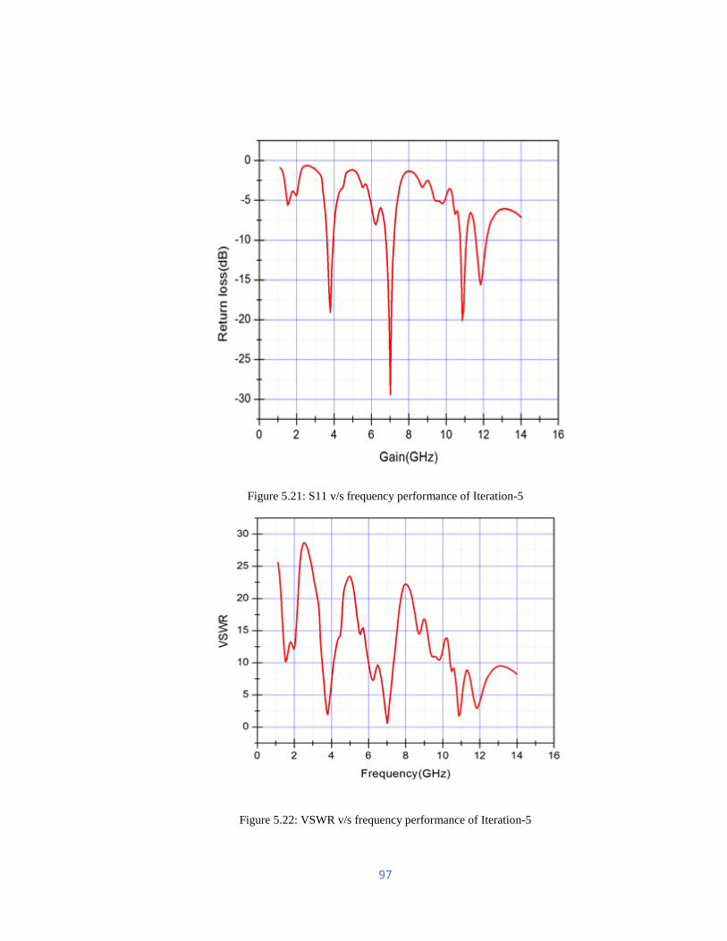
97
Figure 5.21: S11 v/s frequency performance of Iteration-5
Figure 5.22: VSWR v/s frequency performance of Iteration-5
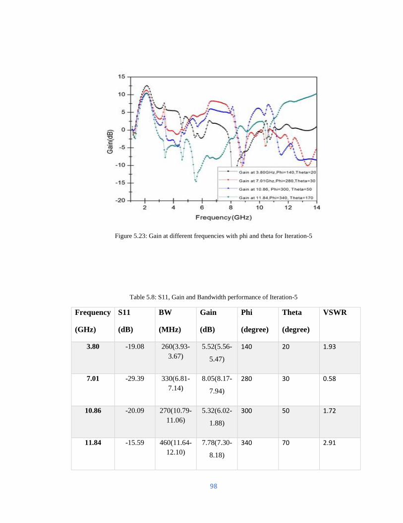
98
Figure 5.23: Gain at different frequencies with phi and theta for Iteration-5
Table 5.8: S11, Gain and Bandwidth performance of Iteration-5
Frequency
(GHz)
S11
(dB)
BW
(MHz)
Gain
(dB)
Phi
(degree)
Theta
(degree)
VSWR
3.80 -19.08 260(3.93-
3.67)
5.52(5.56-
5.47)
140 20 1.93
7.01 -29.39 330(6.81-
7.14)
8.05(8.17-
7.94)
280 30 0.58
10.86 -20.09 270(10.79-
11.06)
5.32(6.02-
1.88)
300 50 1.72
11.84 -15.59 460(11.64-
12.10)
7.78(7.30-
8.18)
340 70 2.91
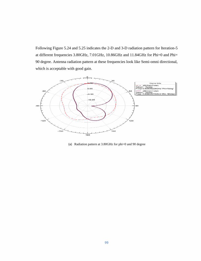
99
Following Figure 5.24 and 5.25 indicates the 2-D and 3-D radiation pattern for Iteration-5
at different frequencies 3.80GHz, 7.01GHz, 10.86GHz and 11.84GHz for Phi=0 and Phi=
90 degree. Antenna radiation pattern at these frequencies look like Semi-omni directional,
which is acceptable with good gain.
(a) Radiation pattern at 3.80GHz for phi=0 and 90 degree
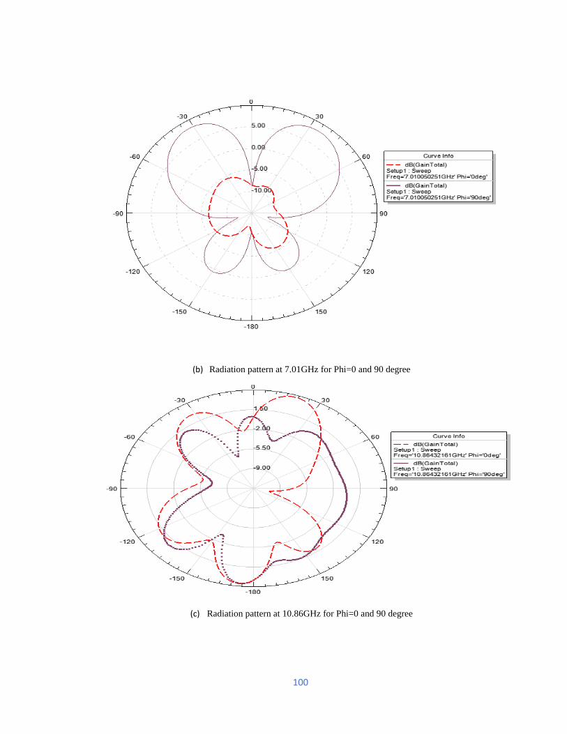
100
(b) Radiation pattern at 7.01GHz for Phi=0 and 90 degree
(c) Radiation pattern at 10.86GHz for Phi=0 and 90 degree
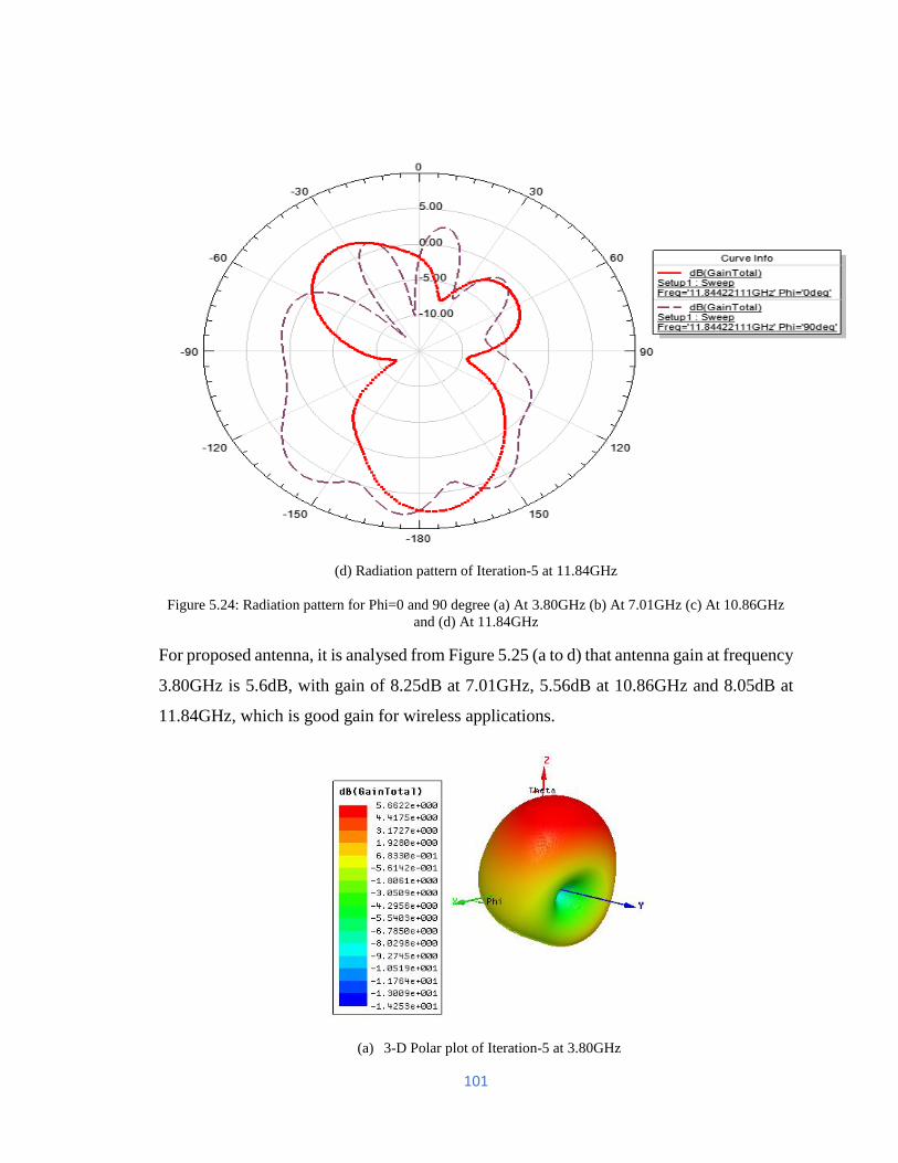
101
(d) Radiation pattern of Iteration-5 at 11.84GHz
Figure 5.24: Radiation pattern for Phi=0 and 90 degree (a) At 3.80GHz (b) At 7.01GHz (c) At 10.86GHz
and (d) At 11.84GHz
For proposed antenna, it is analysed from Figure 5.25 (a to d) that antenna gain at frequency
3.80GHz is 5.6dB, with gain of 8.25dB at 7.01GHz, 5.56dB at 10.86GHz and 8.05dB at
11.84GHz, which is good gain for wireless applications.
(a) 3-D Polar plot of Iteration-5 at 3.80GHz
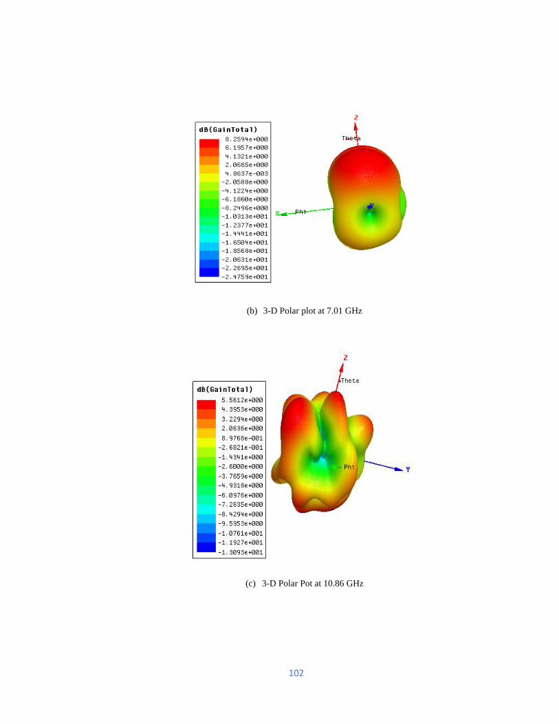
102
(b) 3-D Polar plot at 7.01 GHz
(c) 3-D Polar Pot at 10.86 GHz
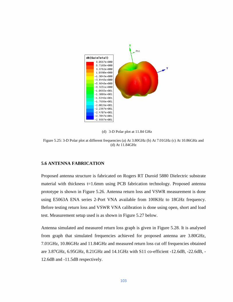
103
(d) 3-D Polar plot at 11.84 GHz
Figure 5.25: 3-D Polar plot at different frequencies (a) At 3.80GHz (b) At 7.01GHz (c) At 10.86GHz and
(d) At 11.84GHz
5.6 ANTENNA FABRICATION
Proposed antenna structure is fabricated on Rogers RT Duroid 5880 Dielectric substrate
material with thickness t=1.6mm using PCB fabrication technology. Proposed antenna
prototype is shown in Figure 5.26. Antenna return loss and VSWR measurement is done
using E5063A ENA series 2-Port VNA available from 100KHz to 18GHz frequency.
Before testing return loss and VSWR VNA calibration is done using open, short and load
test. Measurement setup used is as shown in Figure 5.27 below.
Antenna simulated and measured return loss graph is given in Figure 5.28. It is analysed
from graph that simulated frequencies achieved for proposed antenna are 3.80GHz,
7.01GHz, 10.86GHz and 11.84GHz and measured return loss cut off frequencies obtained
are 3.87GHz, 6.95GHz, 8.21GHz and 14.1GHz with S11 co-efficient -12.6dB, -22.6dB, -
12.6dB and -11.5dB respectively.
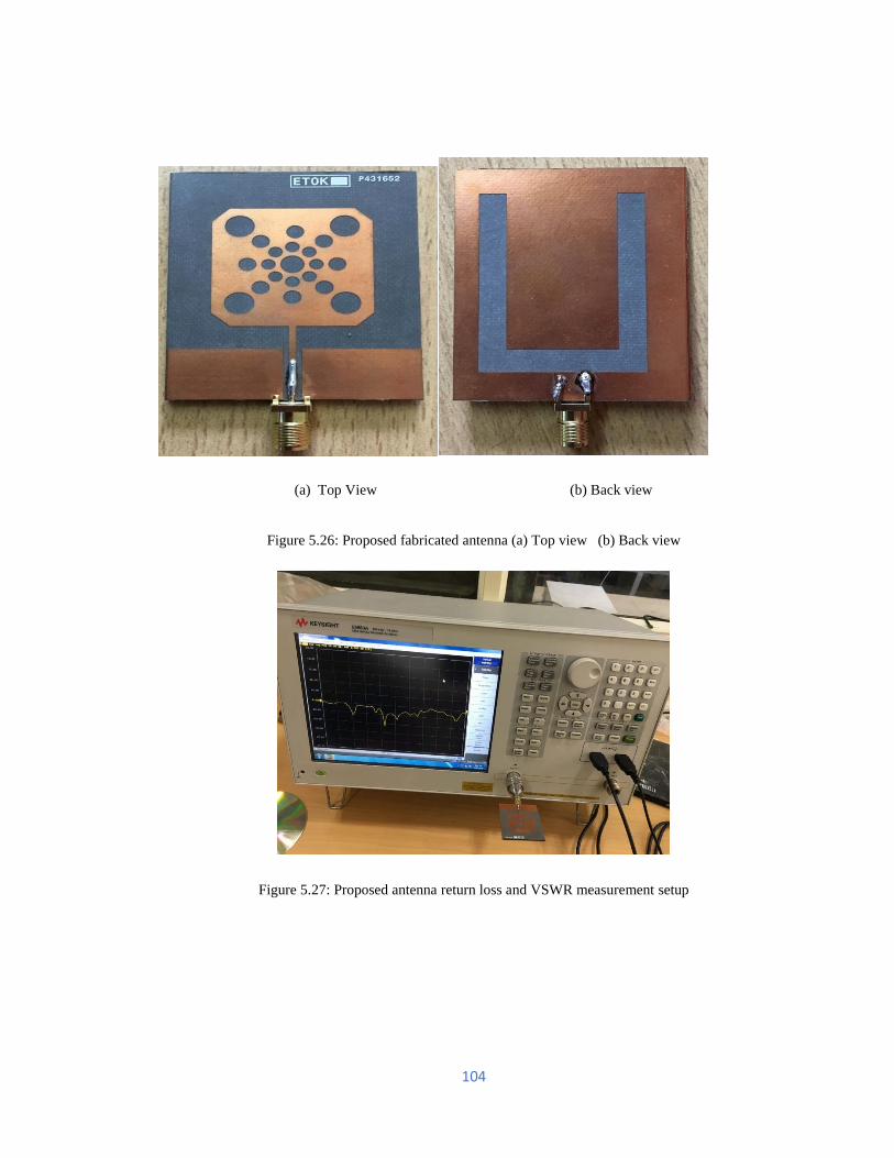
104
(a) Top View (b) Back view
Figure 5.26: Proposed fabricated antenna (a) Top view (b) Back view
Figure 5.27: Proposed antenna return loss and VSWR measurement setup
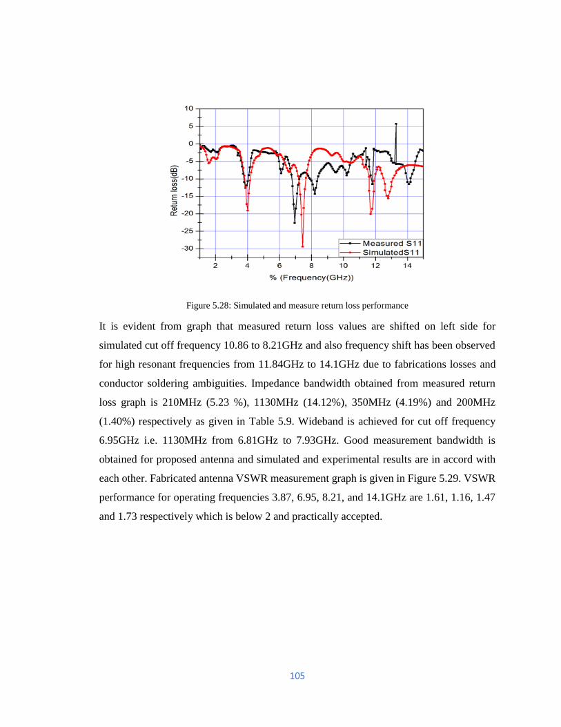
105
Figure 5.28: Simulated and measure return loss performance
It is evident from graph that measured return loss values are shifted on left side for
simulated cut off frequency 10.86 to 8.21GHz and also frequency shift has been observed
for high resonant frequencies from 11.84GHz to 14.1GHz due to fabrications losses and
conductor soldering ambiguities. Impedance bandwidth obtained from measured return
loss graph is 210MHz (5.23 %), 1130MHz (14.12%), 350MHz (4.19%) and 200MHz
(1.40%) respectively as given in Table 5.9. Wideband is achieved for cut off frequency
6.95GHz i.e. 1130MHz from 6.81GHz to 7.93GHz. Good measurement bandwidth is
obtained for proposed antenna and simulated and experimental results are in accord with
each other. Fabricated antenna VSWR measurement graph is given in Figure 5.29. VSWR
performance for operating frequencies 3.87, 6.95, 8.21, and 14.1GHz are 1.61, 1.16, 1.47
and 1.73 respectively which is below 2 and practically accepted.
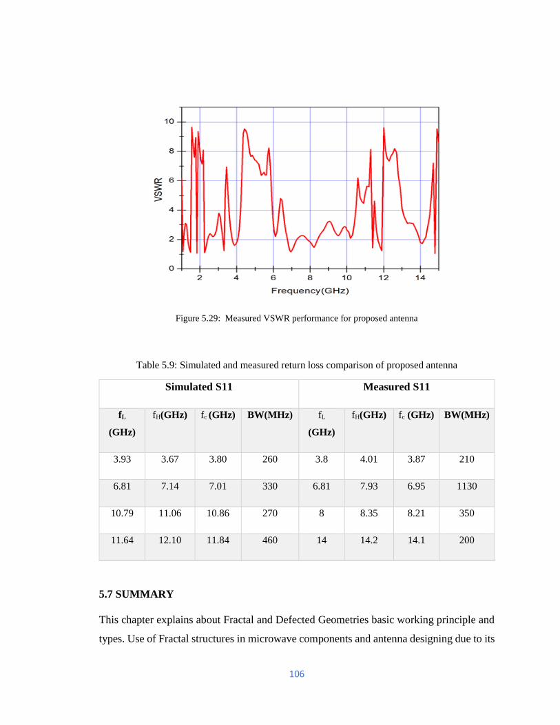
106
Figure 5.29: Measured VSWR performance for proposed antenna
Table 5.9: Simulated and measured return loss comparison of proposed antenna
Simulated S11 Measured S11
fL
(GHz)
fH(GHz) fc (GHz) BW(MHz) fL
(GHz)
fH(GHz) fc (GHz) BW(MHz)
3.93 3.67 3.80 260 3.8 4.01 3.87 210
6.81 7.14 7.01 330 6.81 7.93 6.95 1130
10.79 11.06 10.86 270 8 8.35 8.21 350
11.64 12.10 11.84 460 14 14.2 14.1 200
5.7 SUMMARY
This chapter explains about Fractal and Defected Geometries basic working principle and
types. Use of Fractal structures in microwave components and antenna designing due to its
107
prosperities like space filling and self-symmetry which increases electrical length for flow
of current without changing its physical length to obtain multi band characteristics.
Defected ground structures are used to improve antenna gain and bandwidth by diverting
flow of current in antenna ground. On the basis of these structures, circular cut fractal patch
with U-shaped defected ground with truncated edges microstrip patch antenna is proposed
to achieve multi band behaviour for wireless applications. Antenna performance is
observed in form of return loss, gain, VSWR and bandwidth after studying the effect of
each iteration on design. Proposed antenna is fabricated and simulated and experimental
performance is compared. Antenna is considered as best candidate for wireless
communication applications as practically the best gain considered for all wireless
applications is between 2-3dBi as per the standard bench mark and gain achieved for
proposed antenna is 5.6, 8.25, 5.56 and 8.05dB at 3.80, 7.01, 10.86 and 11.84GHz
frequencies respectively.
108
CHAPTER-6
ELLIPTICAL PATCH MULTI BAND ANTENNA USING FRACTAL
AND DEFECTED GROUND STRUCTURES
6.1. INTRODUCTION
These days, many electronics devices are working on different set of frequencies for
example mobile phone is needed to cover different wireless communication services like
Bluetooth, Wi-Fi, GPS, 4G or LTE and 5G, so multi band antenna are in very high demand
to cover all these applications in single device instead of deploying multiple antenna. In
this chapter, multi band circular patch antenna is designed using fractal and defected
ground structures for various wireless applications using HFSS v15.0 software and
simulated from 1GHz to 15GHz frequency band of operation.
Fractal geometries possess self-similar properties and has the provision to be divided into
parts that is the replica of original design with reduced dimensions. In antenna designing,
multi band and broad band characteristics can be gained using self -similarity property of
fractal structures and these shaped can be fit into available physical dimensions which leads
for compact structures. Depending upon the fractal shape used, current flow virtual lengths
increases and improves the bandwidth and radiation characteristics of antenna. Different
fractal geometries considered are quadrilateral, hexagonal, elliptical, star, spiral etc. but
circular and elliptical shape is chosen due to its excellent performance in gain and
bandwidth. The proposed antenna consists of circular shaped patch design and final patch
structure is achieved using 3 iterations of fractal geometry. Also, in proposed antenna
design, instead of using full length ground plane, defected ground is used to improve
antenna efficiency in terms of antenna parameters.
6.2 ANTENNA DESIGN
Planar microstrip patch antenna comprise of top layer that is called patch, bottom layer
known as ground layer and dielectric substrate sandwiched between two. These PMPA can
109
be designed by etching different structures like square, circular, elliptical, E, H, S etc. on
copper layers of double side PCB. The top patch layer acts as radiator for transmitting
antenna and receptor for receiving antenna, whereas the bottom PCB layer acts as ground
plane which can be plane surface or defected one. In MPA, antenna radiations occur due
to fringing effect between the corners of designed patch structure and the defected ground
plane. Patch antenna can use different geometries to obtain resonate frequency bands for
desired applications. These days’ elliptical patch antenna is gaining much attention due to
their circular polarization characteristics among different patch structures. For today’s
wireless communication systems, broadband and multiple features requirement can be only
fulfilled by elliptical patch fractal antenna.
Figure 6.1, shows the proposed multi band antenna design for wireless applications. The
proposed structure is designed using Rogers RT Duroid 5880 substrate material with
thickness (t= 0.8mm), dielectric constant (εr=2.2), and loss tangent of 0.0009. The RT
Duroid substrate dimensions are 50mm x 50mm x 0.8mm with elliptical shaped patch. To
obtain impedance matching Lumped port with 50-ohm resistance is used with Y-axis and
Z-axis dimensions of 3.87mm and 0.8mm respectively and microstrip feed method is used
for antenna feeding with dimensions 12.94 mm x 3.87mm. To achieve more compactness
in antenna design, elliptical patch with n=3 iterations is used, without changing the physical
length of antenna to obtain multi band characteristics of proposed antenna structure.
Defected ground plan is used to improve antenna performance parameters like bandwidth,
gain and to suppress cross polarization. These structures are used to divert current
distribution in ground plane to change the inductive and capacitive properties of proposed
antenna. Defected ground dimensions considered are 12.7mm x 50mm x 0.8mm.
Fractal curves are characterized by two parameters: indentation factor (IF) and iteration
order (IO). All of these antennas are fabricated on 0.8 mm substrates with relative
permittivity 2.2, and are matched by quarter wavelength transformers. The radius of
elliptical patch changes with number of iterations. As in proposed antenna design, number
of iterations are increasing, the electrical length of antenna patch structure also increases
110
without changing the overall antenna dimensions, thus different resonate bands are
achieved for proposed antenna.
As compared the circular shapes, the elliptical shape has various advantages like it provides
large degree of freedom and flexibility in the antenna design geometry. Other advantages
of elliptical patch over circular patch are to obtain circular polarization by exciting the
elliptical patch compared to rectangular and circular patch, after properly selecting the feed
position of elliptical patch for 50-ohm impedance matching to transfer maximum power
from source to load. Circular polarization can be achieved by positioning the feed point on
a radial line with reference to the major axis. In ellipse the positive side axis gives the left-
hand circular polarization (LHCP) and negative axis provides right hand circular
polarization (RHCP). Moreover, elliptical patch flexibility in antenna design upto large
extents by using concept of eccentricity and focal length to further fine tune antenna to get
desired antenna performance. Also, in antenna design theory, elliptical patch provides more
surface are for flow of electric currents as compared to circular patch for radiating.
In microstrip patch antenna, elliptical shapes are rarely used by researches due to its
difficult mathematical expression and boundary conditions involved during its analysis.
Regular elliptical patch used in microstrip antenna shows narrow bandwidth and gain
performance, so to further enhance bandwidth and gain performance of these antenna,
fractal and defected ground geometry is used. As, shown in this proposed antenna design,
elliptical patch design is implemented using fractal theory with iteration factor n=3.The
radiator or receptor element of proposed antenna is the fractal elliptical shaped patch
structure which is fed by microstrip feed line. In proposed design, each ellipse with
different radii is designed to operate on specific frequency to exhibit multi band
characteristics for this antenna architecture. Final simulated antenna design consists of four
Ellipses, from which the smallest inner ellipse is resonating at high frequency bands due to
its smaller radiation area, whereas, the largest outer ellipse, operates at low frequency
bands due to its large surface resonating area. The remaining two ellipse resonates between
low cut off and high cut of frequencies to obtain wide band characteristics.
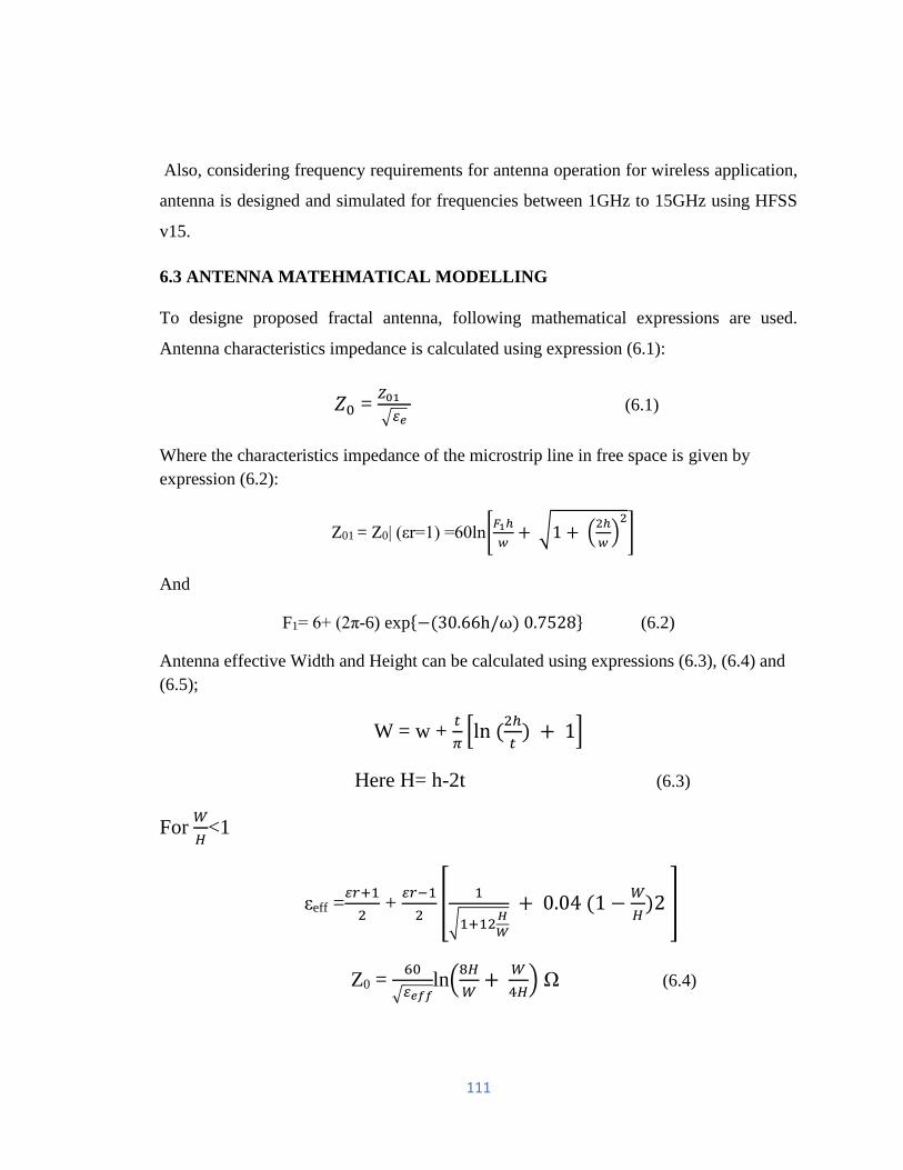
111
Also, considering frequency requirements for antenna operation for wireless application,
antenna is designed and simulated for frequencies between 1GHz to 15GHz using HFSS
v15.
6.3 ANTENNA MATEHMATICAL MODELLING
To designe proposed fractal antenna, following mathematical expressions are used.
Antenna characteristics impedance is calculated using expression (6.1):
𝑍0 = 𝑍01
√𝜀𝑒 (6.1)
Where the characteristics impedance of the microstrip line in free space is given by
expression (6.2):
Z01 = Z0| (εr=1) =60ln[𝐹1ℎ
𝑤+ √1 + (
2ℎ
𝑤)
2
]
And
F1= 6+ (2π-6) exp−(30.66h/ω) 0.7528 (6.2)
Antenna effective Width and Height can be calculated using expressions (6.3), (6.4) and
(6.5);
W = w + 𝑡
𝜋[ln (
2ℎ
𝑡) + 1]
Here H= h-2t (6.3)
For 𝑊
𝐻<1
εeff =𝜀𝑟+1
2 +
𝜀𝑟−1
2[
1
√1+12𝐻
𝑊
+ 0.04 (1 −𝑊
𝐻)2 ]
Z0 = 60
√𝜀𝑒𝑓𝑓ln(
8𝐻
𝑊+
𝑊
4𝐻) Ω (6.4)
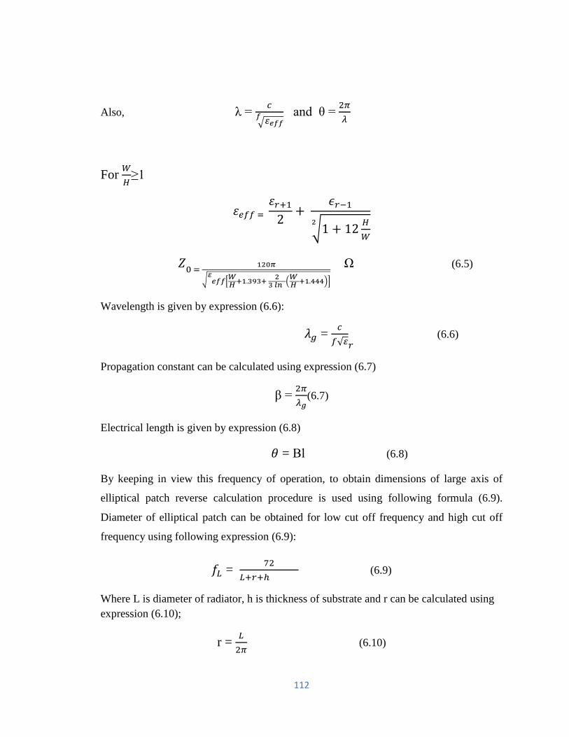
112
Also, λ = 𝑐
√𝜀𝑒𝑓𝑓𝑓 and θ =
2𝜋
𝜆
For 𝑊
𝐻≥1
𝜀𝑒𝑓𝑓 =
𝜀𝑟+1
2+
𝜖𝑟−1
√1 + 12𝐻
𝑊
2
𝑍0 =
120𝜋
√𝜀
𝑒𝑓𝑓[𝑊𝐻
+1.393+ 2
3 𝑙𝑛 (
𝑊 𝐻
+1.444)]
Ω (6.5)
Wavelength is given by expression (6.6):
𝜆𝑔 = 𝑐
𝑓√𝜀𝑟 (6.6)
Propagation constant can be calculated using expression (6.7)
β = 2𝜋
𝜆𝑔(6.7)
Electrical length is given by expression (6.8)
𝜃 = Βl (6.8)
By keeping in view this frequency of operation, to obtain dimensions of large axis of
elliptical patch reverse calculation procedure is used using following formula (6.9).
Diameter of elliptical patch can be obtained for low cut off frequency and high cut off
frequency using following expression (6.9):
𝑓𝐿 = 72
𝐿+𝑟+ℎ (6.9)
Where L is diameter of radiator, h is thickness of substrate and r can be calculated using
expression (6.10);
r = 𝐿
2𝜋 (6.10)
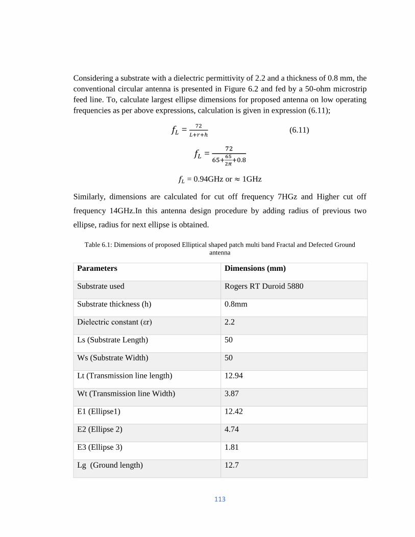
113
Considering a substrate with a dielectric permittivity of 2.2 and a thickness of 0.8 mm, the
conventional circular antenna is presented in Figure 6.2 and fed by a 50-ohm microstrip
feed line. To, calculate largest ellipse dimensions for proposed antenna on low operating
frequencies as per above expressions, calculation is given in expression (6.11);
𝑓𝐿 = 72
𝐿+𝑟+ℎ (6.11)
𝑓𝐿 = 72
65+65
2𝜋+0.8
𝑓𝐿 = 0.94GHz or ≈ 1GHz
Similarly, dimensions are calculated for cut off frequency 7HGz and Higher cut off
frequency 14GHz.In this antenna design procedure by adding radius of previous two
ellipse, radius for next ellipse is obtained.
Table 6.1: Dimensions of proposed Elliptical shaped patch multi band Fractal and Defected Ground
antenna
Parameters Dimensions (mm)
Substrate used Rogers RT Duroid 5880
Substrate thickness (h) 0.8mm
Dielectric constant (εr) 2.2
Ls (Substrate Length) 50
Ws (Substrate Width) 50
Lt (Transmission line length) 12.94
Wt (Transmission line Width) 3.87
E1 (Ellipse1) 12.42
E2 (Ellipse 2) 4.74
E3 (Ellipse 3) 1.81
Lg (Ground length) 12.7
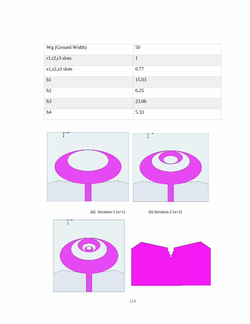
114
Wg (Ground Width) 50
r1,r2,r3 slots 1
s1,s2,s3 slots 0.77
h1 15.03
h2 6.25
h3 23.06
h4 5.33
(a) Iteration-1 (n=1) (b) Iteration-2 (n=2)
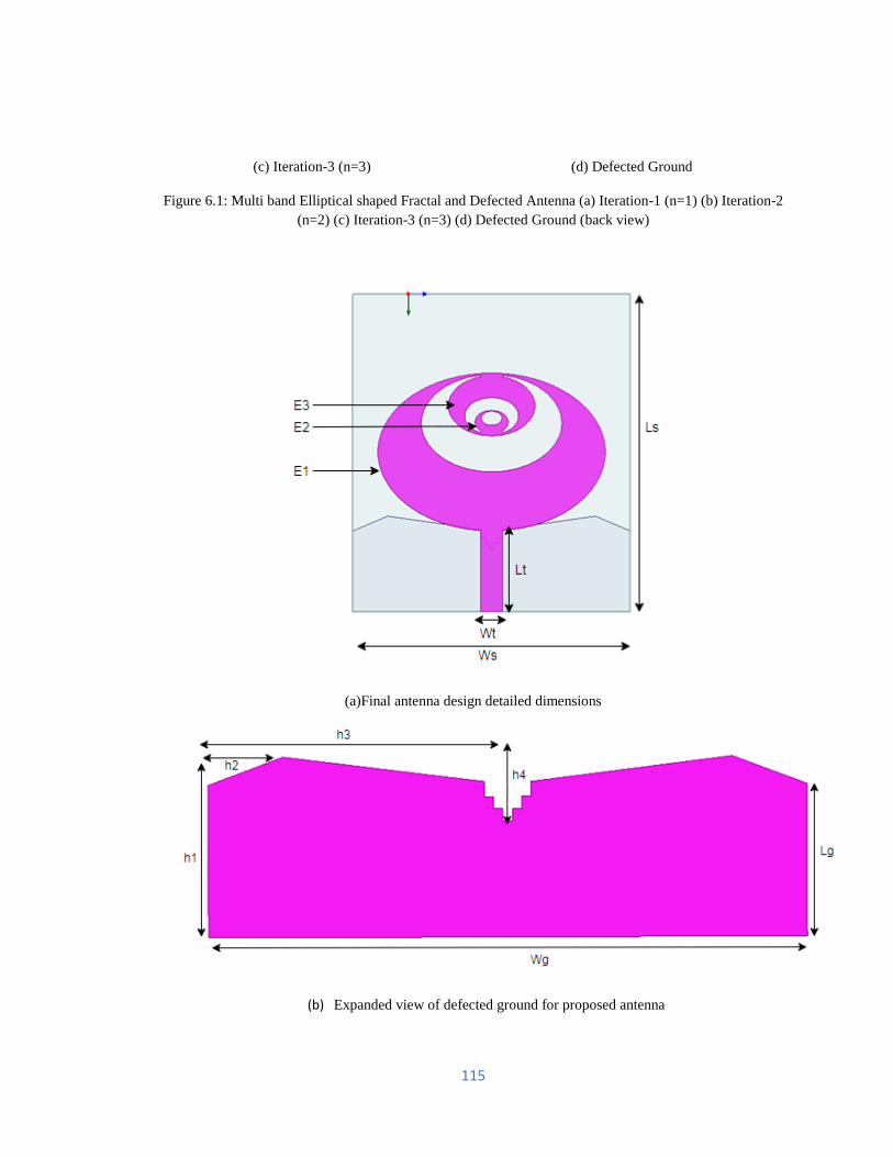
115
(c) Iteration-3 (n=3) (d) Defected Ground
Figure 6.1: Multi band Elliptical shaped Fractal and Defected Antenna (a) Iteration-1 (n=1) (b) Iteration-2
(n=2) (c) Iteration-3 (n=3) (d) Defected Ground (back view)
(a)Final antenna design detailed dimensions
(b) Expanded view of defected ground for proposed antenna
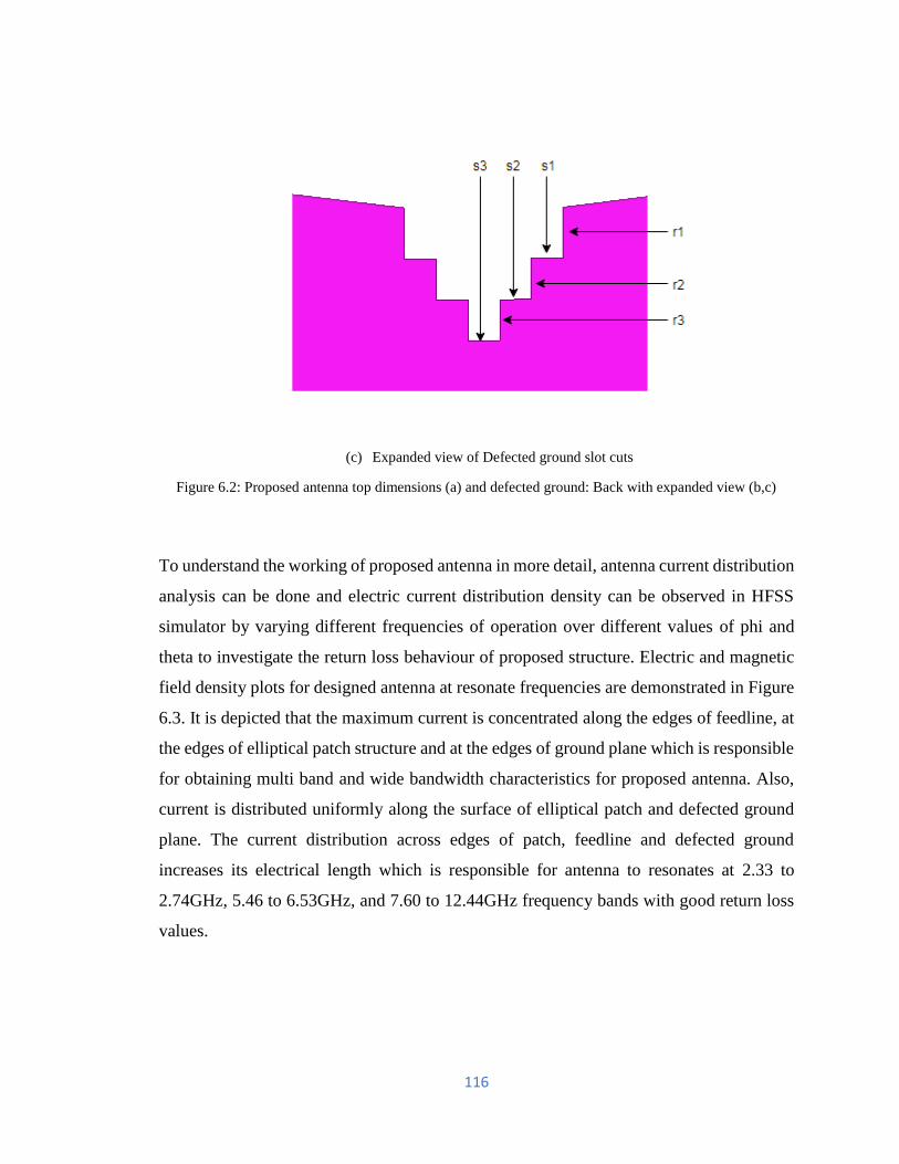
116
(c) Expanded view of Defected ground slot cuts
Figure 6.2: Proposed antenna top dimensions (a) and defected ground: Back with expanded view (b,c)
To understand the working of proposed antenna in more detail, antenna current distribution
analysis can be done and electric current distribution density can be observed in HFSS
simulator by varying different frequencies of operation over different values of phi and
theta to investigate the return loss behaviour of proposed structure. Electric and magnetic
field density plots for designed antenna at resonate frequencies are demonstrated in Figure
6.3. It is depicted that the maximum current is concentrated along the edges of feedline, at
the edges of elliptical patch structure and at the edges of ground plane which is responsible
for obtaining multi band and wide bandwidth characteristics for proposed antenna. Also,
current is distributed uniformly along the surface of elliptical patch and defected ground
plane. The current distribution across edges of patch, feedline and defected ground
increases its electrical length which is responsible for antenna to resonates at 2.33 to
2.74GHz, 5.46 to 6.53GHz, and 7.60 to 12.44GHz frequency bands with good return loss
values.
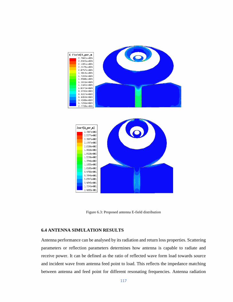
117
Figure 6.3: Proposed antenna E-field distribution
6.4 ANTENNA SIMULATION RESULTS
Antenna performance can be analysed by its radiation and return loss properties. Scattering
parameters or reflection parameters determines how antenna is capable to radiate and
receive power. It can be defined as the ratio of reflected wave form load towards source
and incident wave from antenna feed point to load. This reflects the impedance matching
between antenna and feed point for different resonating frequencies. Antenna radiation
118
properties provide information related to antenna directivity, gain and density of power for
frequency bands over which antenna is resonating. These parameters can be represented in
terms of 2-D or 3-D graphical patterns. To analyse antenna performance, simulation is
carried out using HFSS simulator from 1GHz to 15GHz prior fabrication using PCB
technology. Antenna performance is analysed in terms of return loss, bandwidth, VSWR
and radiation pattern.
Table 6.2: Proposed antenna simulated results in terms of S11, Gain, VSWR and Bandwidth
Frequency
(GHz)
Cut off
frequency
Return loss
(dB)
Bandwidth
(MHz)
VSWR Gain (dB)
2.33-2.74 2.6 -18.18 410 1.2 3.27
5.46-6.53 6 -15.11 1070 1.4 4.37
7.60-12.44 8.2 -16.33 4840 1.35 5.52
Figure 6.4, shows the reflection co-efficient simulated performance of proposed antenna.
It is depicted from graph that proposed antenna shows multi band characteristics with wide
band impedance bandwidth. Antenna resonates over three frequency bands with operating
frequencies 2.6GHz, 6GHz and 8.2GHz with return loss values -18.18, -15.11 and -
16.33dB respectively. Impedance bandwidth achieved over respective band of operation is
14.96 % (2.33 to 2.74), 16.38% (5.46 to 6.53GHz) and 38.90% (7.60 to 12.44GHz)
respectively. For achieved frequency bands of operation VSWR performance is below 2
which is acceptable and its value should be between 1 and 2 practically, VSWR is given in
Figure 6.5.
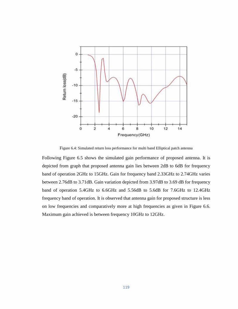
119
Figure 6.4: Simulated return loss performance for multi band Elliptical patch antenna
Following Figure 6.5 shows the simulated gain performance of proposed antenna. It is
depicted from graph that proposed antenna gain lies between 2dB to 6dB for frequency
band of operation 2GHz to 15GHz. Gain for frequency band 2.33GHz to 2.74GHz varies
between 2.76dB to 3.71dB. Gain variation depicted from 3.97dB to 3.69 dB for frequency
band of operation 5.4GHz to 6.6GHz and 5.56dB to 5.6dB for 7.6GHz to 12.4GHz
frequency band of operation. It is observed that antenna gain for proposed structure is less
on low frequencies and comparatively more at high frequencies as given in Figure 6.6.
Maximum gain achieved is between frequency 10GHz to 12GHz.
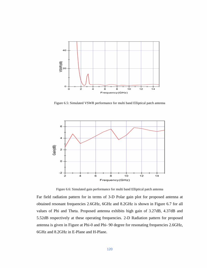
120
Figure 6.5: Simulated VSWR performance for multi band Elliptical patch antenna
Figure 6.6: Simulated gain performance for multi band Elliptical patch antenna
Far field radiation pattern for in terms of 3-D Polar gain plot for proposed antenna at
obtained resonant frequencies 2.6GHz, 6GHz and 8.2GHz is shown in Figure 6.7 for all
values of Phi and Theta. Proposed antenna exhibits high gain of 3.27dB, 4.37dB and
5.52dB respectively at these operating frequencies. 2-D Radiation pattern for proposed
antenna is given in Figure at Phi-0 and Phi- 90 degree for resonating frequencies 2.6GHz,
6GHz and 8.2GHz in E-Plane and H-Plane.
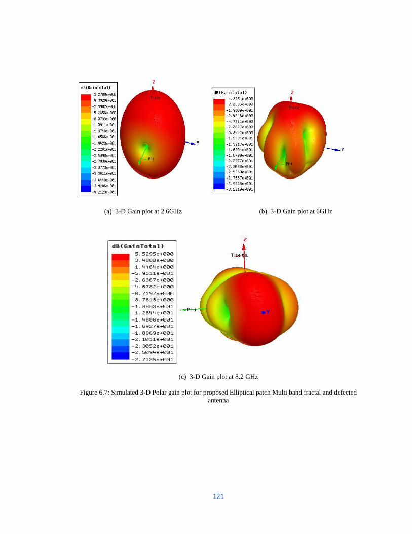
121
(a) 3-D Gain plot at 2.6GHz (b) 3-D Gain plot at 6GHz
(c) 3-D Gain plot at 8.2 GHz
Figure 6.7: Simulated 3-D Polar gain plot for proposed Elliptical patch Multi band fractal and defected
antenna
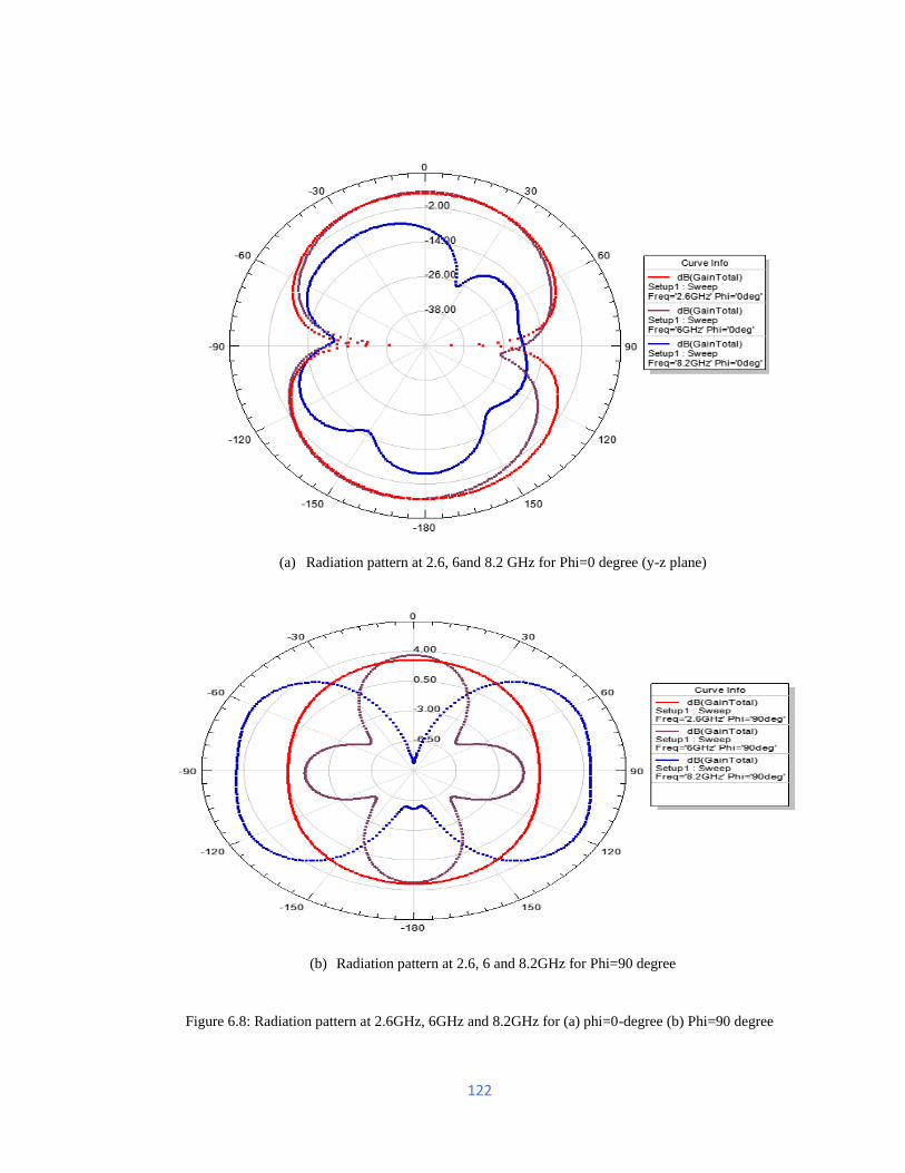
122
(a) Radiation pattern at 2.6, 6and 8.2 GHz for Phi=0 degree (y-z plane)
(b) Radiation pattern at 2.6, 6 and 8.2GHz for Phi=90 degree
Figure 6.8: Radiation pattern at 2.6GHz, 6GHz and 8.2GHz for (a) phi=0-degree (b) Phi=90 degree
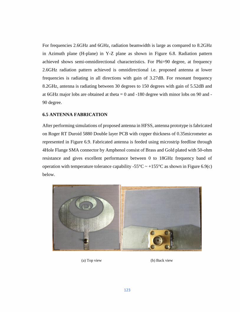
123
For frequencies 2.6GHz and 6GHz, radiation beamwidth is large as compared to 8.2GHz
in Azimuth plane (H-plane) in Y-Z plane as shown in Figure 6.8. Radiation pattern
achieved shows semi-omnidirectional characteristics. For Phi=90 degree, at frequency
2.6GHz radiation pattern achieved is omnidirectional i.e. proposed antenna at lower
frequencies is radiating in all directions with gain of 3.27dB. For resonant frequency
8.2GHz, antenna is radiating between 30 degrees to 150 degrees with gain of 5.52dB and
at 6GHz major lobs are obtained at theta = 0 and -180 degree with minor lobs on 90 and -
90 degree.
6.5 ANTENNA FABRICATION
After performing simulations of proposed antenna in HFSS, antenna prototype is fabricated
on Roger RT Duroid 5880 Double layer PCB with copper thickness of 0.35micrometer as
represented in Figure 6.9. Fabricated antenna is feeded using microstrip feedline through
4Hole Flange SMA connector by Amphenol consist of Brass and Gold plated with 50-ohm
resistance and gives excellent performance between 0 to 18GHz frequency band of
operation with temperature tolerance capability -55°C ~ +155°C as shown in Figure 6.9(c)
below.
(a) Top view (b) Back view
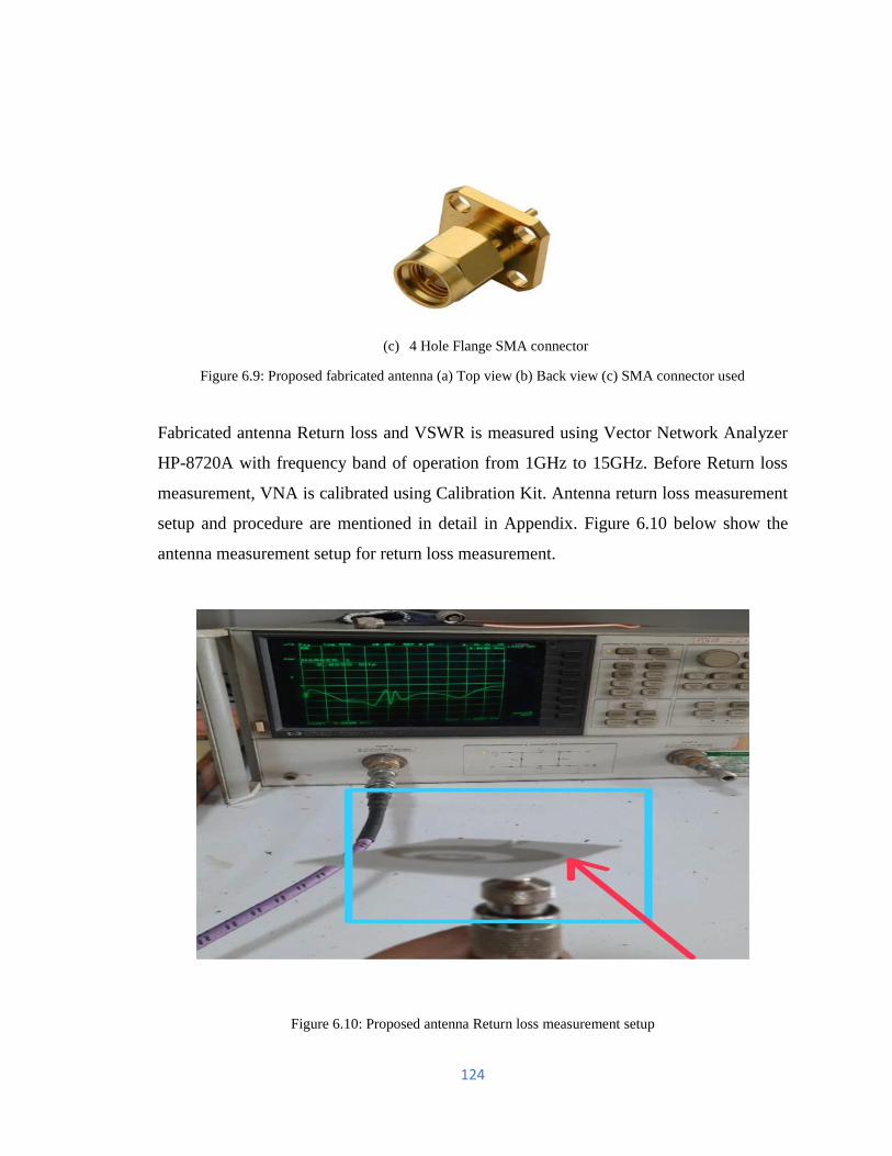
124
(c) 4 Hole Flange SMA connector
Figure 6.9: Proposed fabricated antenna (a) Top view (b) Back view (c) SMA connector used
Fabricated antenna Return loss and VSWR is measured using Vector Network Analyzer
HP-8720A with frequency band of operation from 1GHz to 15GHz. Before Return loss
measurement, VNA is calibrated using Calibration Kit. Antenna return loss measurement
setup and procedure are mentioned in detail in Appendix. Figure 6.10 below show the
antenna measurement setup for return loss measurement.
Figure 6.10: Proposed antenna Return loss measurement setup
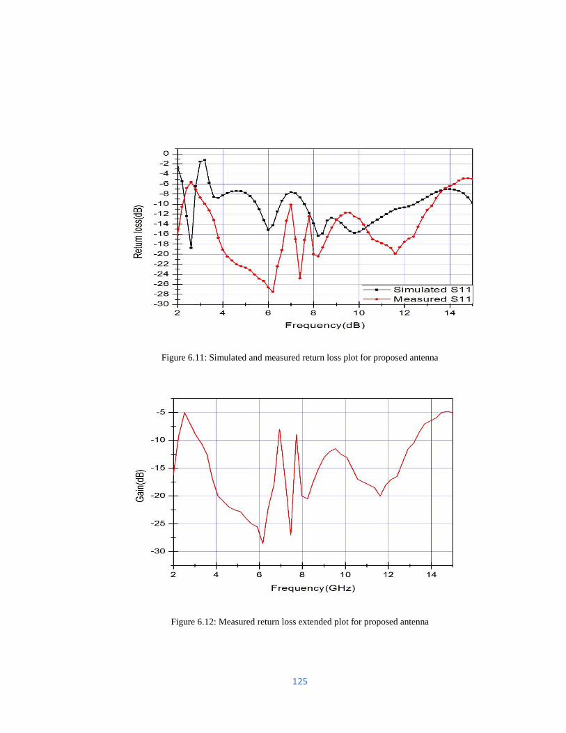
125
Figure 6.11: Simulated and measured return loss plot for proposed antenna
Figure 6.12: Measured return loss extended plot for proposed antenna
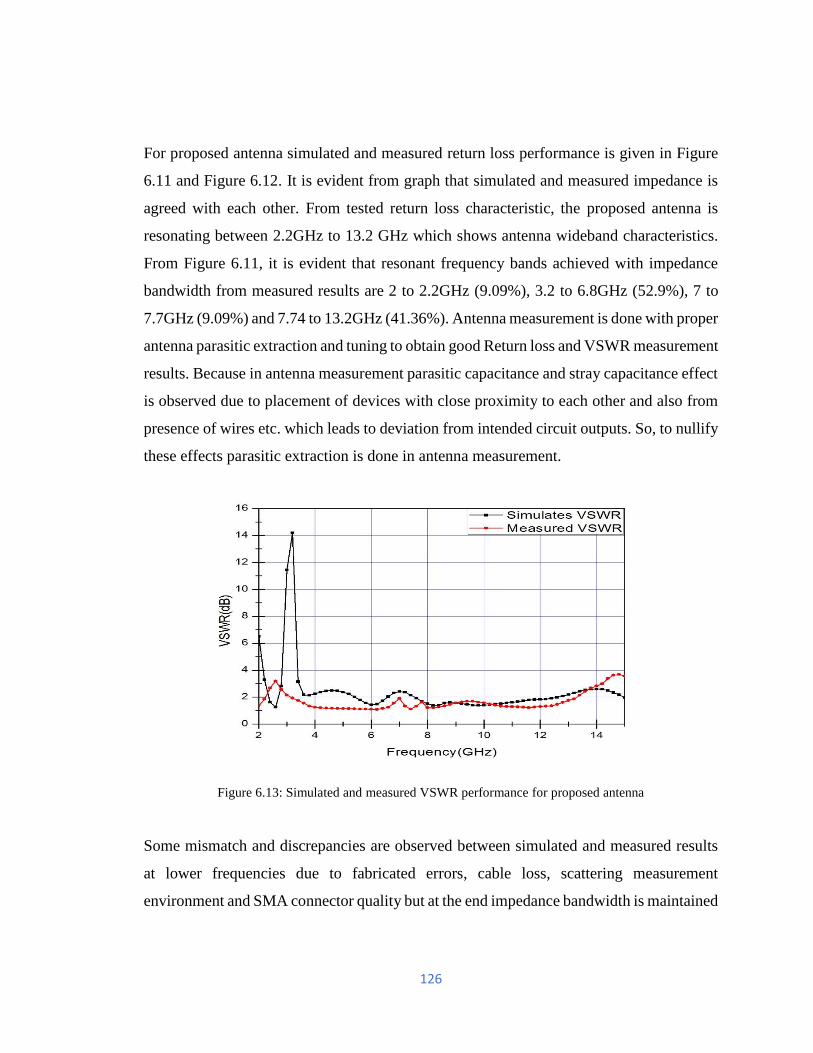
126
For proposed antenna simulated and measured return loss performance is given in Figure
6.11 and Figure 6.12. It is evident from graph that simulated and measured impedance is
agreed with each other. From tested return loss characteristic, the proposed antenna is
resonating between 2.2GHz to 13.2 GHz which shows antenna wideband characteristics.
From Figure 6.11, it is evident that resonant frequency bands achieved with impedance
bandwidth from measured results are 2 to 2.2GHz (9.09%), 3.2 to 6.8GHz (52.9%), 7 to
7.7GHz (9.09%) and 7.74 to 13.2GHz (41.36%). Antenna measurement is done with proper
antenna parasitic extraction and tuning to obtain good Return loss and VSWR measurement
results. Because in antenna measurement parasitic capacitance and stray capacitance effect
is observed due to placement of devices with close proximity to each other and also from
presence of wires etc. which leads to deviation from intended circuit outputs. So, to nullify
these effects parasitic extraction is done in antenna measurement.
Figure 6.13: Simulated and measured VSWR performance for proposed antenna
Some mismatch and discrepancies are observed between simulated and measured results
at lower frequencies due to fabricated errors, cable loss, scattering measurement
environment and SMA connector quality but at the end impedance bandwidth is maintained
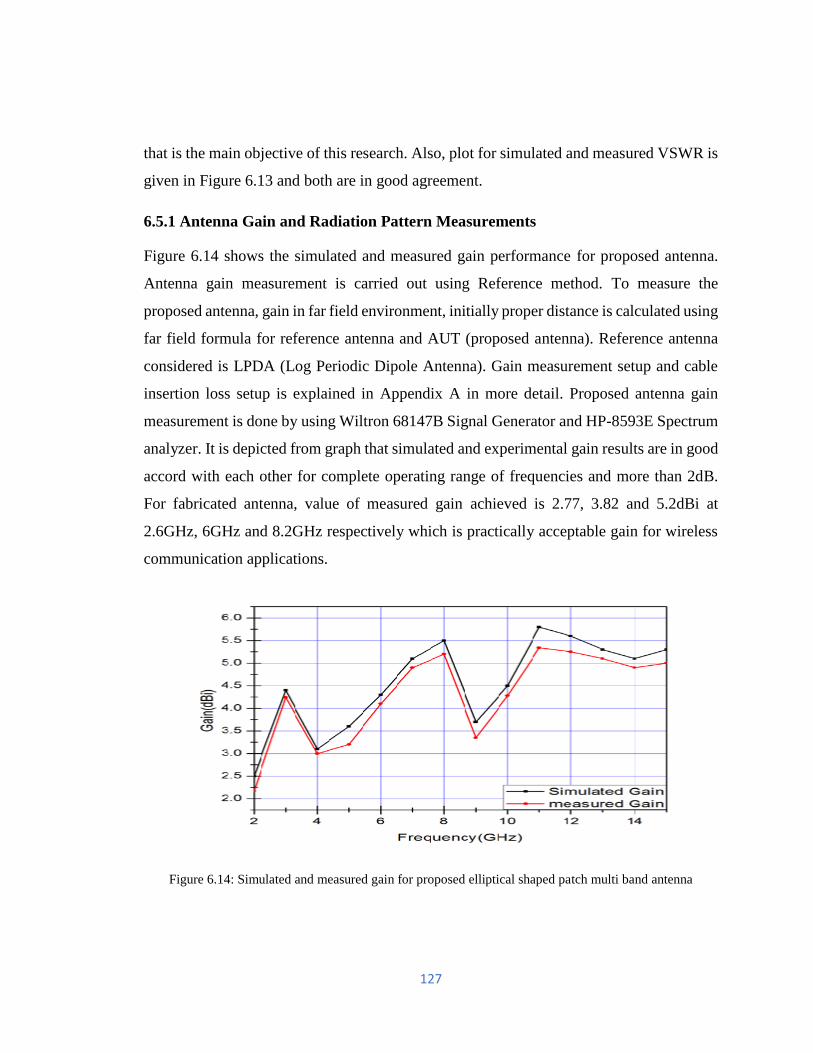
127
that is the main objective of this research. Also, plot for simulated and measured VSWR is
given in Figure 6.13 and both are in good agreement.
6.5.1 Antenna Gain and Radiation Pattern Measurements
Figure 6.14 shows the simulated and measured gain performance for proposed antenna.
Antenna gain measurement is carried out using Reference method. To measure the
proposed antenna, gain in far field environment, initially proper distance is calculated using
far field formula for reference antenna and AUT (proposed antenna). Reference antenna
considered is LPDA (Log Periodic Dipole Antenna). Gain measurement setup and cable
insertion loss setup is explained in Appendix A in more detail. Proposed antenna gain
measurement is done by using Wiltron 68147B Signal Generator and HP-8593E Spectrum
analyzer. It is depicted from graph that simulated and experimental gain results are in good
accord with each other for complete operating range of frequencies and more than 2dB.
For fabricated antenna, value of measured gain achieved is 2.77, 3.82 and 5.2dBi at
2.6GHz, 6GHz and 8.2GHz respectively which is practically acceptable gain for wireless
communication applications.
Figure 6.14: Simulated and measured gain for proposed elliptical shaped patch multi band antenna
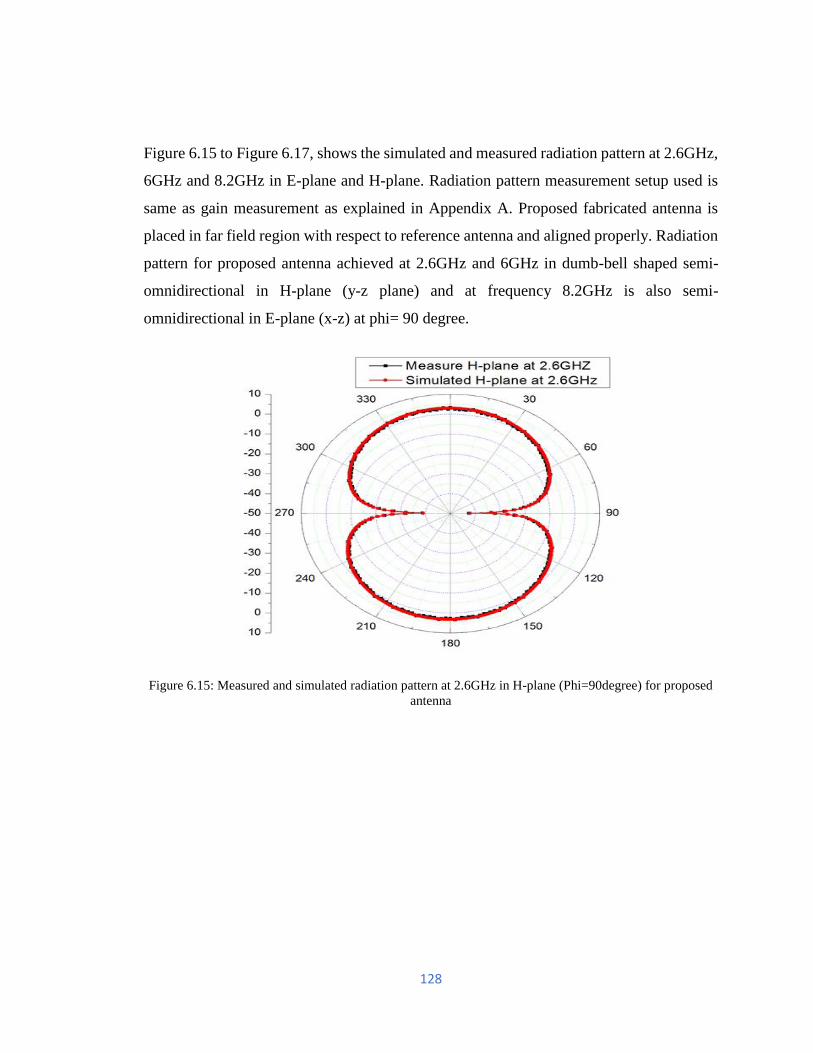
128
Figure 6.15 to Figure 6.17, shows the simulated and measured radiation pattern at 2.6GHz,
6GHz and 8.2GHz in E-plane and H-plane. Radiation pattern measurement setup used is
same as gain measurement as explained in Appendix A. Proposed fabricated antenna is
placed in far field region with respect to reference antenna and aligned properly. Radiation
pattern for proposed antenna achieved at 2.6GHz and 6GHz in dumb-bell shaped semi-
omnidirectional in H-plane (y-z plane) and at frequency 8.2GHz is also semi-
omnidirectional in E-plane (x-z) at phi= 90 degree.
Figure 6.15: Measured and simulated radiation pattern at 2.6GHz in H-plane (Phi=90degree) for proposed
antenna
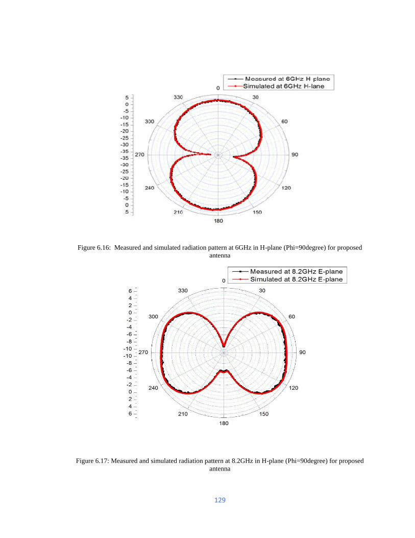
129
Figure 6.16: Measured and simulated radiation pattern at 6GHz in H-plane (Phi=90degree) for proposed
antenna
Figure 6.17: Measured and simulated radiation pattern at 8.2GHz in H-plane (Phi=90degree) for proposed
antenna
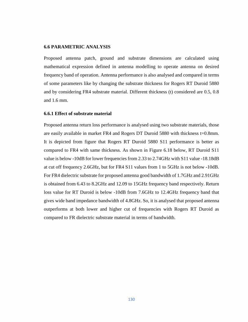
130
6.6 PARAMETRIC ANALYSIS
Proposed antenna patch, ground and substrate dimensions are calculated using
mathematical expression defined in antenna modelling to operate antenna on desired
frequency band of operation. Antenna performance is also analysed and compared in terms
of some parameters like by changing the substrate thickness for Rogers RT Duroid 5880
and by considering FR4 substrate material. Different thickness (t) considered are 0.5, 0.8
and 1.6 mm.
6.6.1 Effect of substrate material
Proposed antenna return loss performance is analysed using two substrate materials, those
are easily available in market FR4 and Rogers DT Duroid 5880 with thickness t=0.8mm.
It is depicted from figure that Rogers RT Duroid 5880 S11 performance is better as
compared to FR4 with same thickness. As shown in Figure 6.18 below, RT Duroid S11
value is below -10dB for lower frequencies from 2.33 to 2.74GHz with S11 value -18.18dB
at cut off frequency 2.6GHz, but for FR4 S11 values from 1 to 5GHz is not below -10dB.
For FR4 dielectric substrate for proposed antenna good bandwidth of 1.7GHz and 2.91GHz
is obtained from 6.43 to 8.2GHz and 12.09 to 15GHz frequency band respectively. Return
loss value for RT Duroid is below -10dB from 7.6GHz to 12.4GHz frequency band that
gives wide band impedance bandwidth of 4.8GHz. So, it is analysed that proposed antenna
outperforms at both lower and higher cut of frequencies with Rogers RT Duroid as
compared to FR dielectric substrate material in terms of bandwidth.
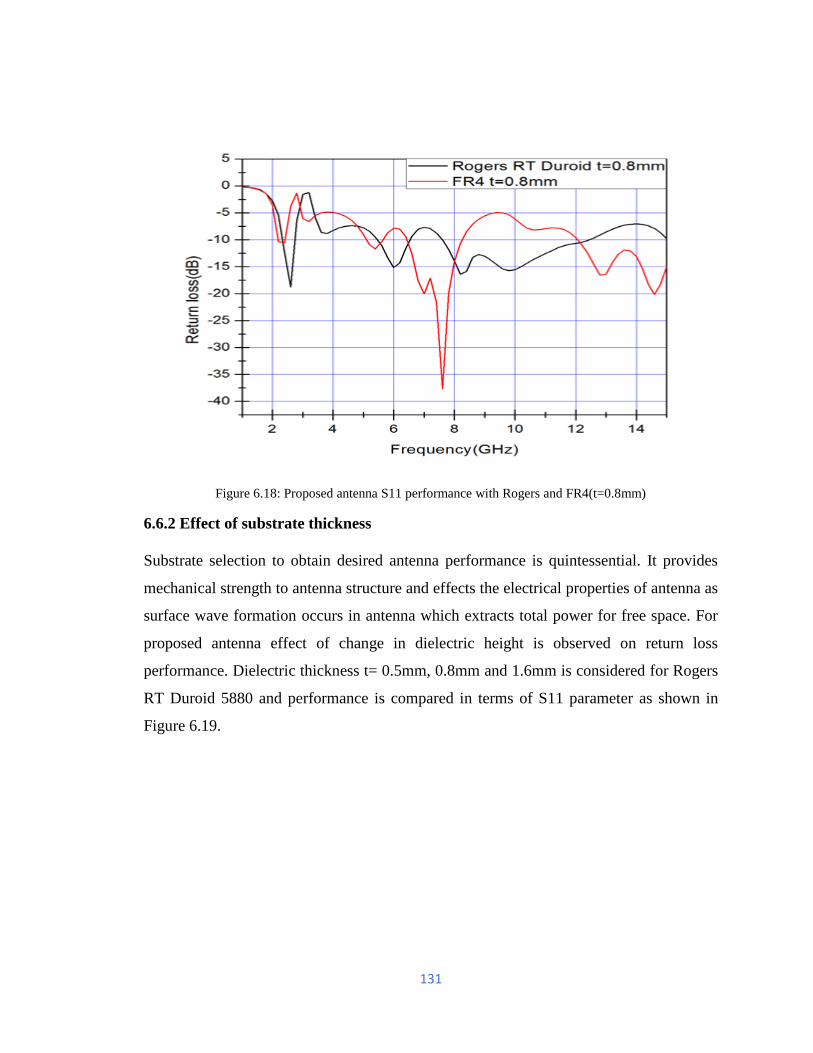
131
Figure 6.18: Proposed antenna S11 performance with Rogers and FR4(t=0.8mm)
6.6.2 Effect of substrate thickness
Substrate selection to obtain desired antenna performance is quintessential. It provides
mechanical strength to antenna structure and effects the electrical properties of antenna as
surface wave formation occurs in antenna which extracts total power for free space. For
proposed antenna effect of change in dielectric height is observed on return loss
performance. Dielectric thickness t= 0.5mm, 0.8mm and 1.6mm is considered for Rogers
RT Duroid 5880 and performance is compared in terms of S11 parameter as shown in
Figure 6.19.
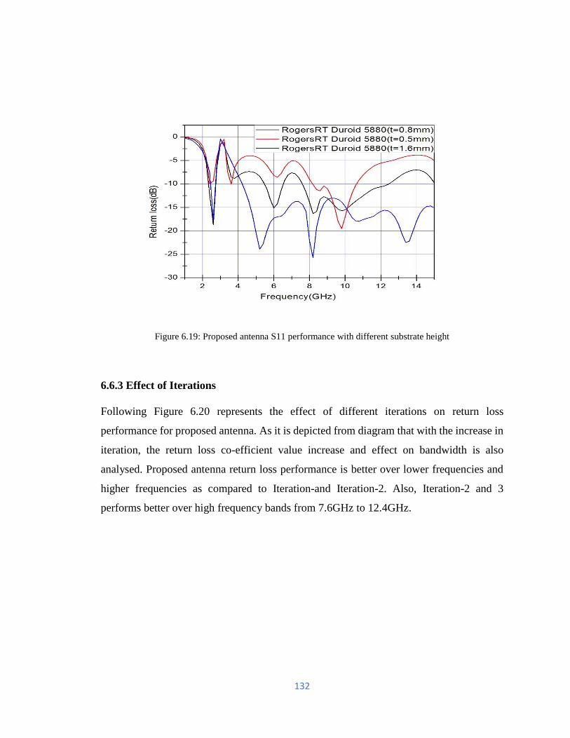
132
Figure 6.19: Proposed antenna S11 performance with different substrate height
6.6.3 Effect of Iterations
Following Figure 6.20 represents the effect of different iterations on return loss
performance for proposed antenna. As it is depicted from diagram that with the increase in
iteration, the return loss co-efficient value increase and effect on bandwidth is also
analysed. Proposed antenna return loss performance is better over lower frequencies and
higher frequencies as compared to Iteration-and Iteration-2. Also, Iteration-2 and 3
performs better over high frequency bands from 7.6GHz to 12.4GHz.
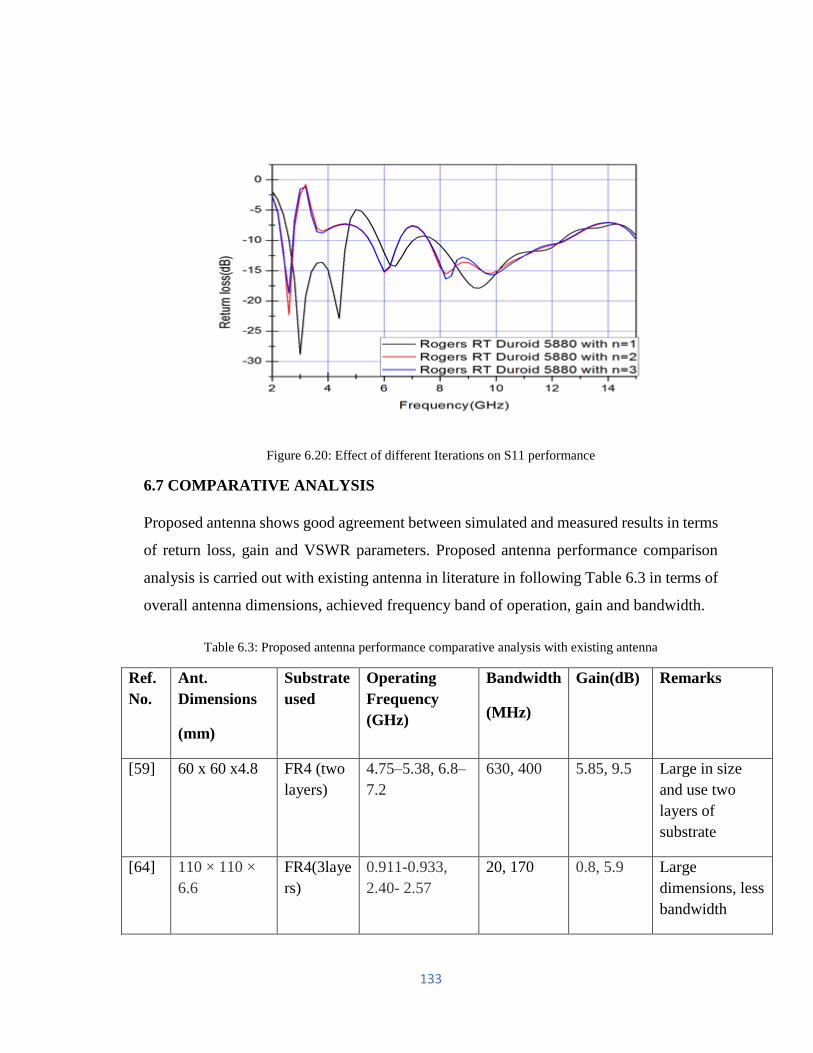
133
Figure 6.20: Effect of different Iterations on S11 performance
6.7 COMPARATIVE ANALYSIS
Proposed antenna shows good agreement between simulated and measured results in terms
of return loss, gain and VSWR parameters. Proposed antenna performance comparison
analysis is carried out with existing antenna in literature in following Table 6.3 in terms of
overall antenna dimensions, achieved frequency band of operation, gain and bandwidth.
Table 6.3: Proposed antenna performance comparative analysis with existing antenna
Ref.
No.
Ant.
Dimensions
(mm)
Substrate
used
Operating
Frequency
(GHz)
Bandwidth
(MHz)
Gain(dB) Remarks
[59] 60 x 60 x4.8 FR4 (two
layers)
4.75–5.38, 6.8–
7.2
630, 400 5.85, 9.5 Large in size
and use two
layers of
substrate
[64] 110 × 110 ×
6.6
FR4(3laye
rs)
0.911-0.933,
2.40- 2.57
20, 170 0.8, 5.9 Large
dimensions, less
bandwidth
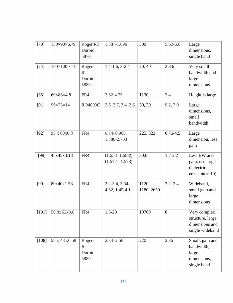
134
[70] 138×90×6.79 Roger RT
Duroid
5870
1.387-1.696 309 5.62-6.6 Large
dimensions,
single band
[74] 100×100 x11 Rogers
RT
Duroid
5880
1.4-1.6, 2-2.4 20, 40 2.3,6 Very small
bandwidth and
large
dimensions
[85] 60×88×4.8 FR4 3.62-4.75 1130 3.4 Height is large
[91] 96×73×14 RO4003C 2.5–2.7, 3.4–3.6 30, 20 9.2, 7.0 Large
dimensions,
small
bandwidth
[92] 95 x 60x0.8 FR4 0.74–0.965,
1.380-2.703
225, 323 0.76-4.5 Large
dimension, less
gain
[98]
45x45x3.18
FR4 (1.558 -1.588),
(1.572 - 1.578)
30,6 1.7-2.2
Less BW and
gain, use large
dielectric
constant(ε=10)
[99] 80x40x1.58 FR4 2.2-3.4, 3.34-
4.52, 1.45-4.1
1120,
1180, 2650
2.2–2.4
Wideband,
small gain and
large
dimensions
[101] 50.8x 62x0.8 FR4 1.3-20 19700 8 Very complex
structure, large
dimensions and
single wideband
[108] 55 x 48 x0.58 Rogers
RT
Duroid
5880
2.34–2.56 220 2.36 Small, gain and
bandwidth,
large
dimensions,
single band
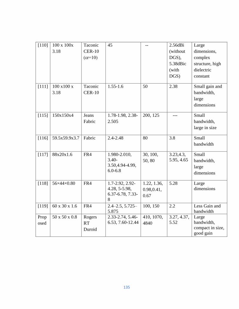
135
[110] 100 x 100x
3.18
Taconic
CER-10
(εr=10)
45 -- 2.56dBi
(without
DGS),
5.38dBic
(with
DGS)
Large
dimensions,
complex
structure, high
dielectric
constant
[111] 100 x100 x
3.18
Taconic
CER-10
1.55-1.6 50 2.38 Small gain and
bandwidth,
large
dimensions
[115] 150x150x4 Jeans
Fabric
1.78-1.98, 2.38-
2.505
200, 125 --- Small
bandwidth,
large in size
[116] 59.5x59.9x3.7 Fabric 2.4-2.48 80 3.8 Small
bandwidth
[117] 88x20x1.6 FR4 1.980-2.010,
3.40-
3.50,4.94-4.99,
6.0-6.8
30, 100,
50, 80
3.23,4.3,
5.95, 4.65
Small
bandwidth,
large
dimensions
[118] 56×44×0.80 FR4 1.7-2.92, 2.92-
4.28, 5-5.98,
6.37-6.78, 7.33-
8
1.22, 1.36,
0.98,0.41,
0.67
5.28 Large
dimensions
[119] 60 x 30 x 1.6 FR4 2.4–2.5, 5.725–
5.875
100, 150 2.2 Less Gain and
bandwidth
Prop
osed
50 x 50 x 0.8 Rogers
RT
Duroid
2.33-2.74, 5.46-
6.53, 7.60-12.44
410, 1070,
4840
3.27, 4.37,
5.52
Large
bandwidth,
compact in size,
good gain
136
6.8 SUMMARY
In this chapter, a compact, low profile elliptical patch multi band fractal microstrip patch
antenna with slotted ground plane is presented and performance is verified with help of
experimental analysis. Parametric analysis is done on proposed antenna by varying
substrate thickness and by changing dielectric substrate material from Rogers RT Duroid
to FR4. It is analysed that antenna is outperforming on Roger RT Duroid with 0.8mm
thickness. Antenna simulation and measured results are in good accord with each other.
Antenna resonates on three different frequencies 2.4, 6 and 8.2GHz with bands 2.33 to
2.74, 5.46 to 6.53, 7.60 to 12.44GHz and impedance bandwidth achieved is 410, 1070 and
4840MHz respectively. Proposed antenna shows wideband and multi band characteristics.
Antenna is very good candidate for wireless applications and covers frequency bands for
Wi-Fi (2.4GHz) Bluetooth version V1.0-V4.0, WLAN (2.4/5.2/5.8GHz), WiMAX
(2.3/2.5/5.5GHz), Wireless Body Area Network (2.3/2.4GHz), RFID (2.4-2.5/5.85-
5.925GHz), Microwave ovens (2.4-2.48GHz) ISM (Industrial Scientific and Medical) band
applications. It also covers RADAR (2.33-2.74/5.4), Geostationary Satellite
communication (11.7-12.2GHz), X-band application (8-12GHz), S-Band (2.3-2.4GHz)
communication, Wireless Communication Services (WCS) 2.345-2.360GHz, and 4G-LTE
(2.3-2.315GHz) wireless communication standards.
137
CHAPTER-7
CONCLUSION AND FUTURE SCOPE
7.1 INTRODUCTION
With tremendous growth in wireless technology, multi band antenna becomes emerging
topic of research. Multi band antenna fulfils indoor and outdoor wireless communication
application requirements over differently specified frequency band of operation. Multi
band Fractal and defected Microstrip patch antenna designed for Wireless communication
application. Antenna is designed and simulated on HFSS simulator. Two different antenna
prototypes are designed and tested based on fractal and defected geometry to obtain multi
band and wide bandwidth characteristic. First antenna is designed with circular cut
truncated edges patch with U-shaped defected ground on Roger RT Duroid 5880 material.
Four resonate frequency bands are achieved 3.80, 7.01, 10.86 and 11.84GHz with
bandwidth of 260, 330, 270 and 460MHz and gain of 5.6, 8.25, 5.56 and 8.05dB
respectively. Second, elliptical shaped fractal patch with step cut defected ground antenna
is simulated and fabricated on Rogers RT Duroid 5880 dielectric substrate. Proposed
structure shows good agreement between simulated and fabricated results in terms of S11,
Gain, Bandwidth and radiation pattern. Antenna performance is analysed after studying
effect of dielectric substrate material used, height of substrate and number of iterations
considered for implementing fractal geometry, on return loss performance. Proposed
antenna is low profile, light in weight, small in size as compared to existing antenna.
Antenna provides 3 resonant frequencies 2.6GHz, 6GHz and 8.2GHz with S11 co-efficient
-18.18, -15.11, -16.33dB and wide impedance bandwidth achieved are 410, 1070 and
4840MHz with good gain. Antenna covers different wireless standards like Wi-Fi
(2.4GHz), Bluetooth version V1.0-V4.0, WLAN (2.4/5.2/5.8GHz), WiMAX
(2.3/2.5/5.5GHz), Wireless Body Area Network (2.3/2.4GHz), RFID (2.4-2.5/5.85-
5.925GHz), Microwave ovens (2.4-2.48GHz) which falls under ISM (Industrial Scientific
and Medical) band applications. It also covers RADAR (2.33-2.74/5.4), Geostationary
Satellite communication (11.7-12.2GHz), X-band application (8-12GHz), S-Band (2.3-
138
2.4GHz) communication, Wireless Communication Services (WCS) 2.345-2.360GHz, and
4GLTE (2.3-2.315GHz) wireless communication standards.
7.2 FUTURE SCOPE
Multi band microstrip patch antenna gain much attention to fulfil demands of wireless
communication application for operation on multiple frequency bands. Microstrip patch
antenna suffers from some short comings like small gain and less bandwidth. In this thesis
work, research is carried out to enhance gain and bandwidth of microstrip patch antenna
using concept of fractal and defected ground structures to achieve high gain, bandwidth
and compact size. This part explains the work that can be extended for future research
work.
1. In this thesis, work is carried out on antenna gain, bandwidth and compact
dimensions using fractal and defected geometry. In future, further gain can be
improved using concept of array for wireless applications.
2. Antenna prototype is simulated and tested for frequencies from 1GHz to 15GHz,
but its performance can be analysed on higher frequencies in terms of return loss,
gain, bandwidth and radiation pattern.
3. Proposed antenna covers ISM frequency bands for WBAN applications, so Specific
Absorption Rate (SAR) analysis can be done for WBAN products.
139
Research Publications
Published Papers
1. A. Kaur and P. K. Malik, "Tri State, T Shaped Circular Cut Ground Antenna for
Higher ‘X’ Band Frequencies," International Conference on Computation,
Automation and Knowledge Management (ICCAKM), Dubai, United Arab
Emirates, pp(s): 90-94, 2020. 10.1109/ICCAKM46823.2020.9051501.
2. Microstrip patch antenna performance analysis with Defected Ground structures: A
review”, Journal of Emerging Technologies and Innovative Research (JETIR),
ISSN: 2349-5162, January 2019.
3. Amandeep Kaur, Praveen Kumar Malik, “Microstrip Antenna Design with
Truncated Edges for Bandwidth Improvement for Wireless Applications”,
International Conference on Recent Innovations in Computing (ICRIC-2020).
(Available online in SN eproofing)
4. Amandeep Kaur, Praveen Kumar Malik, Ramendra Singh, “Planar Rectangular
Micro-strip Patch Antenna Design for 25 GHz Wireless Applications” International
Conference on Recent Innovations in Computing (ICRIC-2020). (Available online
in SN eproofing)
5. Amandeep Kaur, Praveen Kumar Malik, “Multiband Elliptical Fractal and
Defected Ground Structures Microstrip Antenna for Wireless Applications”,
International Journal of Communication Systems. (2nd review accepted)
Papers Communicated
1. Amandeep Kaur and Praveen Kumar Malik, “Adoption of Micro-strip Patch
Antenna for Wireless Communication: Opportunities and Challenges”, Journal of
Electromagnetic Waves and Applications.
Patent
Published:
1.WIDE BAND MICRO-STRIP ANTENNA DESIGN FOR HIGHER X BAND, Patent
ID: 1099.
In process:
1. Multiband Fractal and Defected Microstrip patch antenna for wireless
applications.
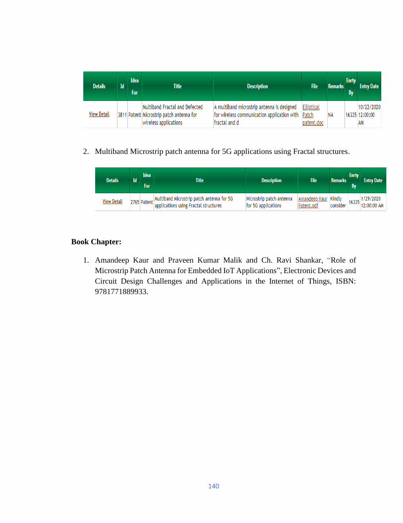
140
2. Multiband Microstrip patch antenna for 5G applications using Fractal structures.
Book Chapter:
1. Amandeep Kaur and Praveen Kumar Malik and Ch. Ravi Shankar, “Role of
Microstrip Patch Antenna for Embedded IoT Applications”, Electronic Devices and
Circuit Design Challenges and Applications in the Internet of Things, ISBN:
9781771889933.
141
APPENDIX A
A.1 ANTENNA FABRICATION
Antenna designing process is carried out in Antenna design and simulation software HFSS.
After converting the HFSS file into Gerber files antenna fabrication process starts. For
Microstrip patch antenna, PCB fabrication technology is used. With the increase in
fabrication demands of electronics components on smaller boards, boost-up the need of
PCB fabrication technology. PCB is a board that provides the mechanical strength to
components and provides connectivity between them through copper tracks. PCB can be
single layer, double layer or multi-layer boards. Main components of PCB are substrate,
copper layers and solder mask. Dielectric material should have low value of dielectric
constant and dielectric loss to achieve good radiation performance of antenna. Selection of
dielectric constant material depends on applications. Dielectric materials with thick
substrate and low dielectric constant provide high bandwidth and better antenna efficiency
but leads to large size structures. On contrary, material with high dielectric constant give
rise to more surface waves and less bandwidth is achieved due to this. For proposed antenna
designing dielectric substrate selected is Rogers RT Duroid with dielectric constant 2.2 and
thickness of 0.8mm to get better antenna efficiency. RT Duroid material is also available
in 0.5, 1.6, 2.4 and 3.2mm thickness. Most commonly used material is FR-4 Epoxy but it
is highly lossy material, so Rogers RT Duroid material is selected for antenna fabrication.
PCB board used is Double layer with copper layers of 0.35micrometer thickness on both
sides.
For PCB fabrication some steps and followed. Initially, design is prepared on software than
Gerber files are created. For creating Gerber files, software used is Dip Trace. It provides
the complete information related to copper layers, solder mask and component notation
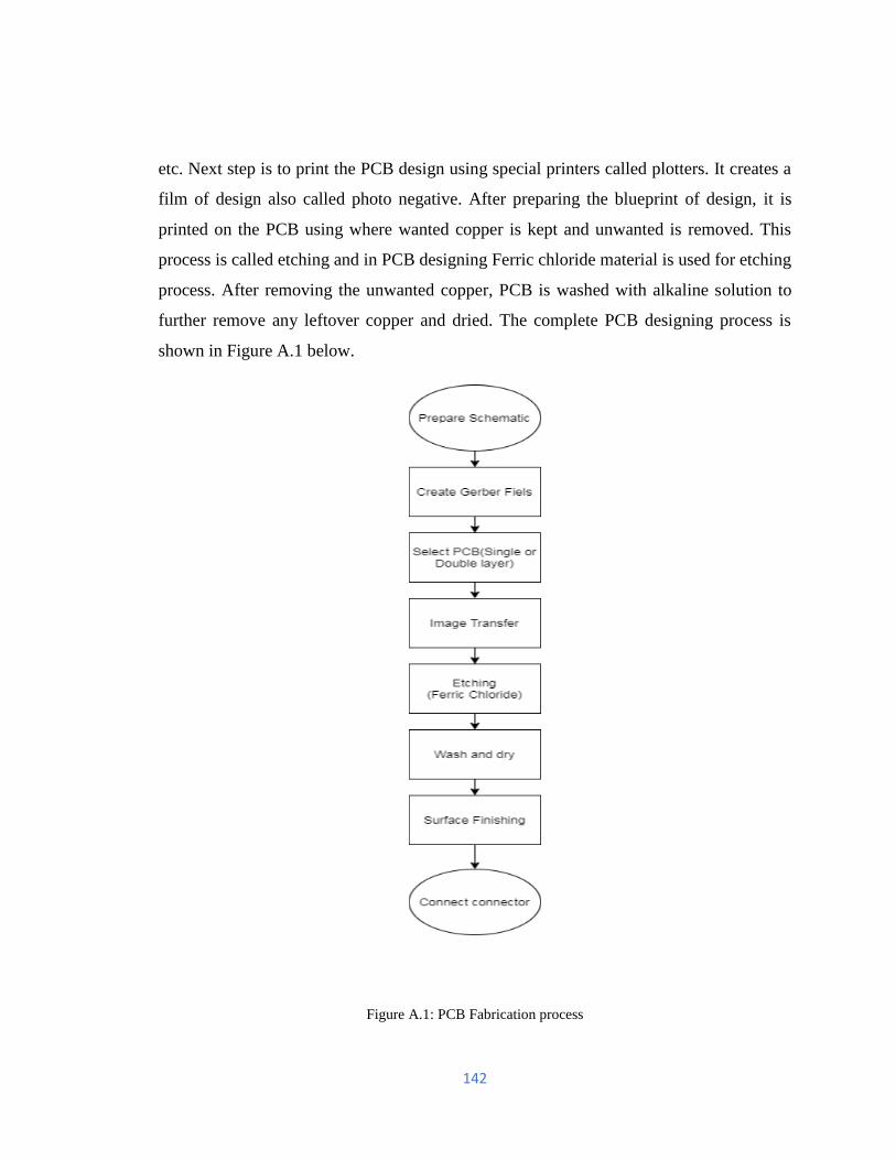
142
etc. Next step is to print the PCB design using special printers called plotters. It creates a
film of design also called photo negative. After preparing the blueprint of design, it is
printed on the PCB using where wanted copper is kept and unwanted is removed. This
process is called etching and in PCB designing Ferric chloride material is used for etching
process. After removing the unwanted copper, PCB is washed with alkaline solution to
further remove any leftover copper and dried. The complete PCB designing process is
shown in Figure A.1 below.
Figure A.1: PCB Fabrication process
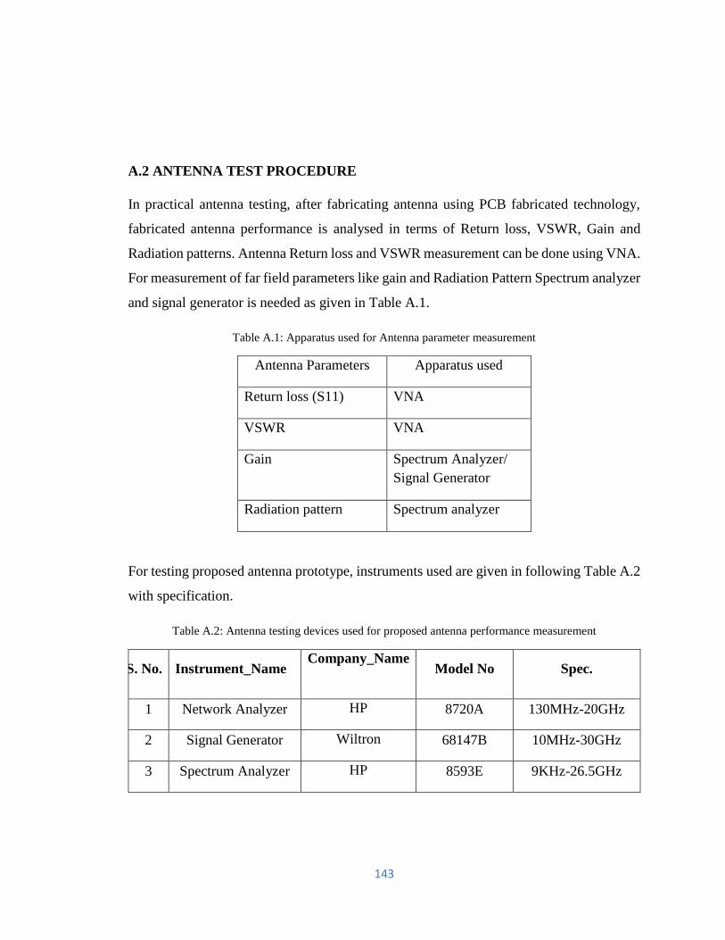
143
A.2 ANTENNA TEST PROCEDURE
In practical antenna testing, after fabricating antenna using PCB fabricated technology,
fabricated antenna performance is analysed in terms of Return loss, VSWR, Gain and
Radiation patterns. Antenna Return loss and VSWR measurement can be done using VNA.
For measurement of far field parameters like gain and Radiation Pattern Spectrum analyzer
and signal generator is needed as given in Table A.1.
Table A.1: Apparatus used for Antenna parameter measurement
Antenna Parameters Apparatus used
Return loss (S11) VNA
VSWR VNA
Gain Spectrum Analyzer/
Signal Generator
Radiation pattern Spectrum analyzer
For testing proposed antenna prototype, instruments used are given in following Table A.2
with specification.
Table A.2: Antenna testing devices used for proposed antenna performance measurement
S. No. Instrument_Name Company_Name
Model No Spec.
1 Network Analyzer HP 8720A 130MHz-20GHz
2 Signal Generator Wiltron 68147B 10MHz-30GHz
3 Spectrum Analyzer HP 8593E 9KHz-26.5GHz
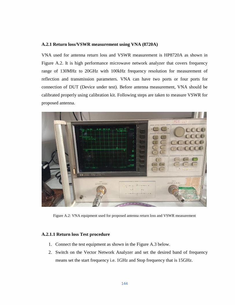
144
A.2.1 Return loss/VSWR measurement using VNA (8720A)
VNA used for antenna return loss and VSWR measurement is HP8720A as shown in
Figure A.2. It is high performance microwave network analyzer that covers frequency
range of 130MHz to 20GHz with 100kHz frequency resolution for measurement of
reflection and transmission parameters. VNA can have two ports or four ports for
connection of DUT (Device under test). Before antenna measurement, VNA should be
calibrated properly using calibration kit. Following steps are taken to measure VSWR for
proposed antenna.
Figure A.2: VNA equipment used for proposed antenna return loss and VSWR measurement
A.2.1.1 Return loss Test procedure
1. Connect the test equipment as shown in the Figure A.3 below.
2. Switch on the Vector Network Analyzer and set the desired band of frequency
means set the start frequency i.e. 1GHz and Stop frequency that is 15GHz.
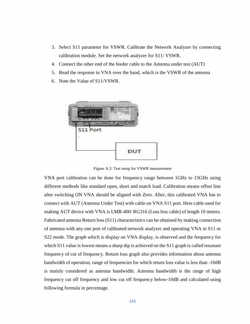
145
3. Select S11 parameter for VSWR. Calibrate the Network Analyzer by connecting
calibration module. Set the network analyzer for S11/ VSWR.
4. Connect the other end of the feeder cable to the Antenna under test (AUT)
5. Read the response in VNA over the band, which is the VSWR of the antenna
6. Note the Value of S11/VSWR.
Figure A.3: Test setup for VSWR measurement
VNA port calibration can be done for frequency range between 1GHz to 15GHz using
different methods like standard open, short and match load. Calibration means offset line
after switching ON VNA should be aligned with Zero. After, this calibrated VNA has to
connect with AUT (Antenna Under Test) with cable on VNA S11 port. Here cable used for
making AUT device with VNA is LMR-400/ RG316 (Loss less cable) of length 10 meters.
Fabricated antenna Return loss (S11) characteristics can be obtained by making connection
of antenna with any one port of calibrated network analyzer and operating VNA in S11 or
S22 mode. The graph which is display on VNA display, is observed and the frequency for
which S11 value is lowest means a sharp dip is achieved on the S11 graph is called resonant
frequency of cut of frequency. Return loss graph also provides information about antenna
bandwidth of operation, range of frequencies for which return loss value is less than -10dB
is mainly considered as antenna bandwidth. Antenna bandwidth is the range of high
frequency cut off frequency and low cut off frequency below-10dB and calculated using
following formula in percentage.
146
Bandwidth (%age) = 𝑓ℎ− 𝑓𝑙
𝑓𝑐 x 100 (A.1)
Where, 𝑓ℎrepresents the higher -10dB point on graph, 𝑓𝑙 denotes the lowest -10dB point on
graph and fc is the cut of frequency with minimum return loss value,
` ` A.2.2 Antenna Gain measurement
Antenna gain is the measurement of antenna power transmitted by antenna under test in a
given direction. Antenna gain in given direction is expressed as the ratio of radiation
intensity in given direction to the total input power. Antenna gain represents the antenna
directivity and antenna electrical efficiency as expressed by expression (A.2).
Gain = 4𝜋𝑅𝑎𝑑𝑖𝑎𝑡𝑖𝑜𝑛 𝐼𝑛𝑡𝑒𝑛𝑠𝑖𝑡𝑦
𝑇𝑜𝑡𝑎𝑙 𝐼𝑛𝑝𝑢𝑡 𝑃𝑜𝑤𝑒𝑟 (A.2)
Antenna gain measurement cab be done using (1) two antenna method (2) Reference
antenna method. Proposed antenna gain measurement is done using reference antenna
method. Reference antenna considered is LPDA (Long Periodic Dipole Array) wideband
antenna. The AUT is placed in far field range of the reference antenna considered. Far
field distance is calculated using far field formula given in expression (A.3). Antenna gain
measurement is done in free space. Gain of AUT is measured with reference to the power
signal received or detected by reference antenna.
Far field ≥ 2𝐷2
𝜆
λ = 𝑠𝑝𝑒𝑒𝑑 𝑜𝑓 𝑙𝑖𝑔ℎ𝑡
𝑓𝑟𝑒𝑞𝑢𝑒𝑛𝑐𝑦 (A.3)
Here, D=Antenna length or Diameter and f= operating frequency
Both Reference antenna and AUT antenna are mounted on tunable and proper distance is
maintained between them for gain measurement. Before antenna gain measurement,
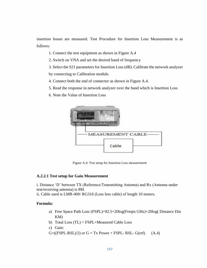
147
insertion losses are measured. Test Procedure for Insertion Loss Measurement is as
follows:
1. Connect the test equipment as shown in Figure A.4
2. Switch on VNA and set the desired band of frequency
3. Select the S21 parameters for Insertion Loss (dB). Calibrate the network analyzer
by connecting to Calibration module.
4. Connect both the end of connector as shown in Figure A.4.
5. Read the response in network analyzer over the band which is Insertion Loss
6. Note the Value of Insertion Loss
Figure A.4: Test setup for Insertion Loss measurement
A.2.2.1 Test setup for Gain Measurement
i. Distance ‘D’ between TX (Reference/Transmitting Antenna) and Rx (Antenna under
test/receiving antenna) is 8M.
ii. Cable used is LMR-400/ RG316 (Loss less cable) of length 10 meters.
Formula:
a) Free Space Path Loss (FSPL)=92.5+20log(Freqin GHz)+20log( Distance Din
KM)
b) Total Loss (TL) = FSPL+Measured Cable Loss
c) Gain:
G=((FSPL-RSL)/2) or G = Tx Power + FSPL- RSL- G(ref) (A.4)
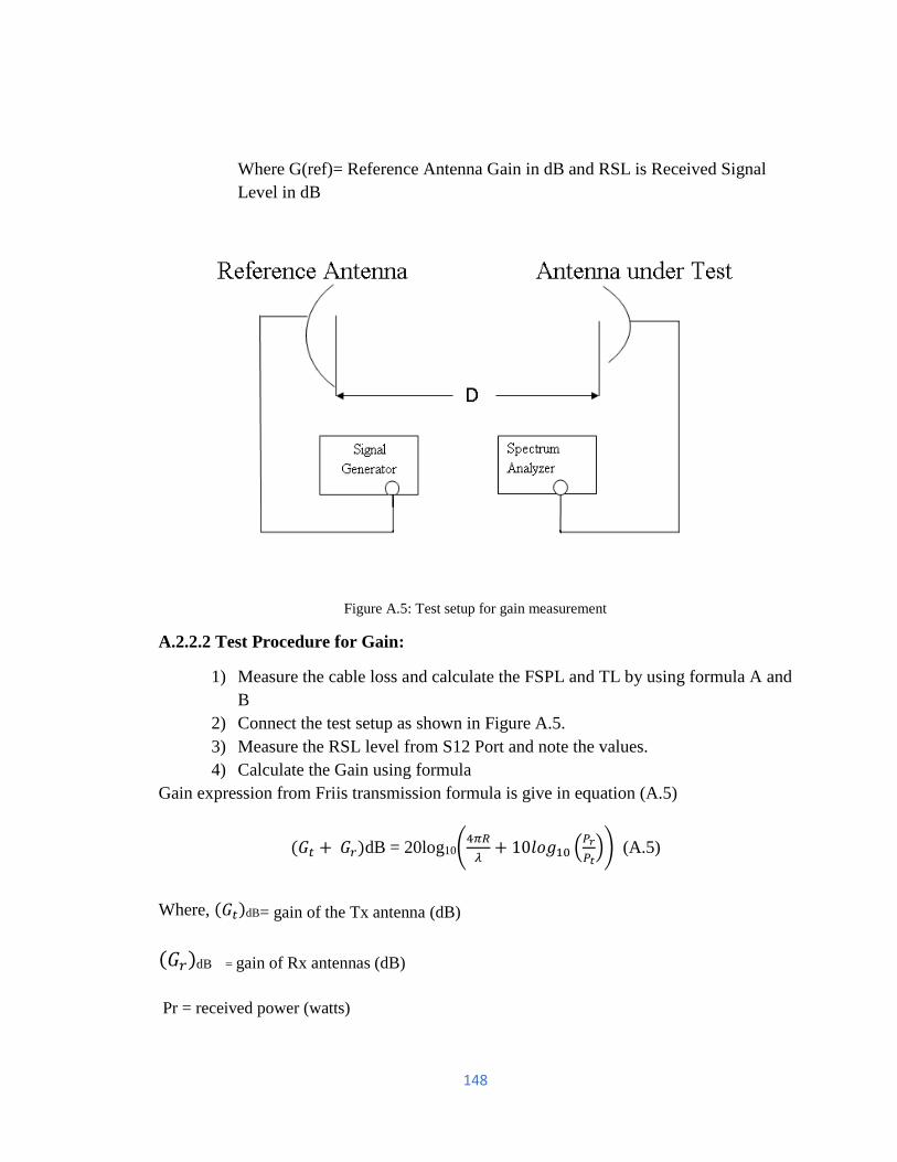
148
Where G(ref)= Reference Antenna Gain in dB and RSL is Received Signal
Level in dB
Figure A.5: Test setup for gain measurement
A.2.2.2 Test Procedure for Gain:
1) Measure the cable loss and calculate the FSPL and TL by using formula A and
B
2) Connect the test setup as shown in Figure A.5.
3) Measure the RSL level from S12 Port and note the values.
4) Calculate the Gain using formula
Gain expression from Friis transmission formula is give in equation (A.5)
(𝐺𝑡 + 𝐺𝑟)dB = 20log10(4𝜋𝑅
𝜆+ 10𝑙𝑜𝑔10 (
𝑃𝑟
𝑃𝑡)) (A.5)
Where, (𝐺𝑡)dB= gain of the Tx antenna (dB)
(𝐺𝑟)dB = gain of Rx antennas (dB)
Pr = received power (watts)
149
Pt = transmitted power (watts)
R =Distance between antenna (m)
λ = signal wavelength (m)
A.2.3 RADIATION PATTERN MEASUREMENT
Antenna measurement setup used for Gain and Radiation pattern measurement is same.
Radiation pattern of antenna represents the measurement of antenna power density
transmitted in particular direction. Antenna radiation pattern measurement is carried out to
analyse fabricated antenna radiation in far field region and comparison is done between
simulated and measured patterns to validate antenna performance for specific application.
For radiation pattern measurement, antenna under test is placed in far field region with
respect to reference antenna used.

150
Bibliography [1] Tapan K Sarkar, “History of Wireless”, John Wiley and Sons, 2006.
[2] Theodore S. Rappaport, “Wireless Communications Principles and Practice Pearson”, 2nd Edition 2002.
[3] Balanis C. A, “Microstrip Antennas”, Antenna Theory, Analysis and Design, Third Edition, John Wiley
& Sons, 2010.
[4] K.D Prasad, “Antenna wave and propagation”, Satya Parkashan, 1983.
[5] Kin-Lu. Wong, “Planar Antennas for Wireless Communications” by Wiley Interscience, 2003.
[6] J. Q Howell, “Microstrip Antennas,” IEEE International Symposium on Antennas and Propagation
Society, pp(s): 177-180, Vol.10, 1972
[7]J. Barreiros , P. Cameirao, C. Peixeiro, “Microstrip patch antenna for GSM 1800 handsets”, IEEE
International Symposium on Antennas and Propagation Society, 06 August 2002.
[8] Yong-Sun Shin , Won-I Kwak, Seong-Ook Park, “ GSM/DCS/IMT-2000 triple-band built-in antenna for
wireless terminals”, IEEE Antennas and Wireless Propagation Letters,Vol.3, pp(s): 104 – 107, 2004.
[9] D. Caratelli , R. Cicchetti , G. Bit-Babik, A. Faraone, “A perturbed E-shaped patch antenna for wideband
WLAN applications”, IEEE Transactions on Antennas and Propagation, Vol. 54 , Issue: 6 , pp(s):1871 –
1874, 2006.
[10] Xiaoxiang He , Sheng Hong , Qishan Zhang ; Emmanouil Manos M. Tentzeris, “Design of a Novel
High-Gain Dual-Band Antenna for WLAN Applications”, IEEE Antennas and Wireless Propagation
Letters”, Vol. 8, pp(s):798 – 801, 2009.
151
[11] L. Lu, J.C. Coetzee, “Reduced-size microstrip patch antenna for Bluetooth applications”, Electronics
Letters, Vol. 41 , Issue: 17, pp(s): 944 – 945, 2005.
[12]Yong-Ling Ban , Jin-Hua Chen , Li-Jun Ying , Joshua Le-Wei Li , Yu-Jiang Wu, “Ultrawideband
Antenna for LTE/GSM/UMTS Wireless USB Dongle Applications”, IEEE Antennas and Wireless
Propagation Letters, Vol.11, pp(s): 403 – 406, 2012.
[13] Qian Wang, Ning Mu, LingLi Wang, Safieddin Safavi-Naeini, and JingPing Liu, “5G MIMO Conformal
Microstrip Antenna Design”, Wireless Communications and Mobile Computing, Vol. 2017, pp(s):1-11,
https://doi.org/10.1155/2017/7616825.
[14] Rashmitha R, Niran N, Abhinandan Ajit Jugale, Mohammed Riyaz Ahmed, “Microstrip Patch Antenna
Design for Fixed Mobile and Satellite 5G Communications”, Procedia Computer Science, Vol.171, pp(s):
2073-2079, 2020. https://doi.org/10.1016/j.procs.2020.04.223
[15] Aksha Mushtaq , Sindhu Hak Gupta , Asmita Rajawat, “Design and Performance Analysis of LoRa
LPWAN Antenna for IoT Applications”, IEEE7th International Conference on Signal Processing and
Integrated Networks (SPIN), April 2020.
[16]PichitpongSoontornpipit, “A Dual-band Compact Microstrip Patch Antenna for 403.5 MHz and 2.45
GHz On-body Communications”, Procedia Computer Science, Vol. 86, pp(s): 232-235, 2016.
https://doi.org/10.1016/j.procs.2016.05.105.
[17] Qudsia Rubani, Sindhu Hak Gupta, Arun Kumar,” Design and analysis of circular patch antenna for
WBAN at terahertz frequency”, Elsevier Optik, Vol. 185, Pages 529-536, May 2019.
https://doi.org/10.1016/j.ijleo.2019.03.142.
[18] Punith S, Praveenkumar S K, Abhinandan Ajit Jugale, Mohammed Riyaz Ahmed, “A Novel Multi band
Microstrip Patch Antenna for 5G Communications”, ScienceDirect Procedia Computer Science, Vol. 171,
pp(s): 2080-2086, 2020. 10.1016/j.procs.2020.04.224

152
[19] Guterman ,Moreira ,Peixeiro, “Microstrip fractal antennas for multistandard terminals”, IEEE Letters
on Antennas and Wireless Propagation, Vol.3, pp(s): 351-354,2004. 10.1109/LAWP.2004.840253.
[20] Kuem C. Hwang, “A Modified Sierpinski Fractal Antenna for Multi band Application”, IEEE Letters
on Antennas and Wireless Propagation , Vol.6, pp(s):357 – 360, October 2007.
[21] X. L. Bao , G. Ruvio , M. J. Ammann , M. John, “ A Novel GPS Patch Antenna on a Fractal Hi-
Impedance Surface Substrate”, IEE Letters on Antenna and Wireless Propagation, Vol.5, pp(s): 323 – 326,
July 2006.
[22] K. Seol, J. Jung, and J. Choi, “Multi-band monopole antenna with inverted U-shaped parasitic plane,”
Electronics Letters, Vol.42, No. 15, pp(s): 844–845, 2006.
[23] R.V. Hara Prasad, Y. Purushottam , V.C. Misra , N. Ashok, “Microstrip fractal patch antenna for multi
band communication”, Electronics Letters, Vol.36 , Issue: 14 , pp(s): 1179 – 1180, Jul 2000.
[24] A. B. Abdel-Rahman, A. K. Verma, A. Boutejdar, and A. S. Omar, “Control of bandstop response of
Hi-Lo microstrip low-pass filter using slot in ground plane”, IEEE Transactions on Microwave Theory and
Techniques, Vol. 52, Issue. 3, pp(s): 1008-1013, March 2004.
[25] C. S. Kim, J. S. Lim, S. Nam, K. Y. Kang, and D. Ahn, “Equivalent circuit modeling of spiral defected
ground structure for microstrip line”, Electronic Letters, Vol. 38, Issue. 19, pp(s):1109-1110, September
2002.
[26] D. J. Woo, T. K. Lee, J. W. Lee, C. S. Pyo, and W. K. Choi, “Novel U-Slot and V-Slot DGSs for
bandstop filter with improved Q factor”, IEEE Transactions on Microwave Theory and Techniques, Vol. 54,
Issue. 6, pp(s):2840-2847, June 2006.
[27] M. K. Mandal and S. Sanyal, “A novel defected ground structure for planar circuits”, IEEE Letters on
Microwave Wireless Components, Vol. 16, Issue. 2, pp(s):93-95, Feb. 2006.
[28] H. J. Chen, T. H. Huang, C. S. Chang, L. S. Chen, N. F. Wang, Y. H. Wang, and M. P. Houng, “A novel
cross-shape DGS applied to design ultra-wide stopband low-pass filters,” IEEE letters on Microwave
WirelessComponents, Vol. 16, Issue. 5, pp(s): 252-254, May 2006.
[29] D. Guha, S. Biswas, M. Biswas, J. Y. Siddiqui, and Y. M. M. Antar, “Concentric ring-shaped defected
ground structures for microstrip applications,” IEEE Letters on Antennas Wireless Propagation, Vol. 5, pp(s):
402-405, 2006.

153
[30] Girish Kumar, K.P. Ray, “Broadband Microstrip Antennas”, Artech House, 2002.
[31] W. L. Stutzman, Polarization in Electromagnetic Systems, MA: Artech House, 1993.
[32] James, J. R., and P. S. Hall, Handbook of Microstrip Antennas, Vol. 1, London: Peter Peregrinus Ltd.,
1989.
[33] Bhatacharya, A. K., and R. Garg, “Generalized Transmission Line Model for Microstrip Patches”, IEE
Proceedings Microwaves, Antennas and Propagation, Pt. H, Vol. 132, No. 2, pp(s): 93–98, 1985.
[34] S. Babu, I. Singh, and G. Kumar, “Improved Linear Transmission Line Model for Rectangular, Circular
and Triangular Microstrip Antennas”, IEEE Antenna and Propagation Theory International Symposium
Digest, pp(s): 614–617, July 1997.
[35] Y. T. Lo, D. Solomon, and W. F. Richards, “Theory and Experiment on Microstrip Antennas”, IEEE
Transactions on Antennas Propagation, Vol. AP-27, pp(s):137–145, March 1979.
[36] W. F. Richards, Y. T. Lo, and D. D. Harrison, ‘‘An Improved Theory for Microstrip Antennas and
Applications”, IEEE Transactions on Antennas PropagationVol. AP-29, pp(s): 38–46, January 1981.
[37] T. Lo, and S. W. Lee, Antenna Handbook, New York: Van Nostrand Reinhold,1988.
[38]T. Okoshi, and T. Miyoshi, “The Planar Circuit-An Approach to Microwave Integrated Circuitry”, IEEE
Transactions on Microwave Theory and Techniques, Vol. 20, Issue.4, pp(s): 245–252, April 1971.
[39] K. C. Gupta, and P. C. Sharma, “Segmentation and De-segmentation Techniques for the Analysis of
Two Dimensional Microstrip Antennas”, IEEE AP-S International Symposium Digest, pp(s):19–22, 1981.
[40] E. H. Newman, and P. Tulyathan, “Analysis of Microstrip Antennas Using Method of Moments”, IEEE
Transactions Antennas Propagation, Vol. AP-29, pp(s):47–53, January 1981, 10.1109/TAP.1981.1142532.
[41] P. Silvester, “Finite Element Analysis of Planar Microwave Network”, IEEE Transactions Microwave
Theory and Techniques, Vol. 21, Issue-2, pp(s):104–108, 1973.
[42] H. F. Lee, and W. Chen, Advances in Microstrip and Printed Antennas, New York: John Wiley & Sons,
1997.
[43] T. Itoh, and W. Menzel, “A Full-Wave Analysis Method for Open Microstrip Structure”, IEEE
Transactions Antennas Propagation, Vol. 29, pp(s): 63–68, January 1981.

154
[44] Young-Bae Jung, Soon-Young Eom, and Soon-Ik Jeon, “Novel Antenna System Design for Sat.llite
Mobile Multimedia Service”, IEEE transactions on Vehicular technology, Vol-59, pp(s): 4237-4247, Issue-
9, 2010.
[45] Yikai Chen, Shiwen Yang, and Zaiping Nie, “Bandwidth Enhancement Method for Low Profile E-
Shaped Microstrip Patch Antennas”, IEEE Transactions on Antennas and Propagation, Vol.58, Issue- 7,
pp(s):2442- 2247, 2010.
[46] Hussein Attia, Leila Yousefi, Omar Ramahi, “High-Gain Patch Antennas Loaded with High
Characteristic Impedance Superstrates”, IEEE Letters on Antenna and Wireless propagation, Vol.10, pp(s):
858-861, 2011.
[47] Ramona Cosmina Hadarig, María Elena de Cos, Fernando Las-Heras, “On the Bandwidth Enhancement
of Patch Antenna Using EBG/AMC Structures”, IEEE 6th European Conference on Antennas and
Propagation (EUCAP), pp(s): 2853-2857, 2011.
[48] Soumyojit Sinha, Anjumanara Begam, “Design of Probe Feed Micro-strip Patch Antenna in S-Band”,
International Journal of Electronics and Communication Engineering, Vol.5, Issue-4, pp(s): 417-423, 2012.
[49] Y. Sung, “Bandwidth Enhancement of a Microstrip Line-Fed Printed Wide-Slot Antenna With a
Parasitic Center Patch”, IEEE Transactions on Antennas and Propagation, Vol.60, Issue-4, pp(s): 1712-1716,
2012.
[50] S. T. Fan, Y. Z. Yin, B. Lee, W.Hu, X. Yang, “Bandwidth Enhancement of a Printed Slot Antenna With
a Pair of Parasitic Patches”, IEEE letters on Antennas and Wireless Propagation, Vol.11, pp(s): 1230-1233,
2012.
[51] P. A. Ambresh, G. M. Pushpanjali, A. A. Sujata, P. M. Hadalgi, P. V. Hunagund, “S-Band compact
microstrip antenna with slots”, National conference on Challenges in research & Technology in the coming
Decades(CRT 2013), pp(s): 1-3, 2013.
[52] Syeda Fizzah Jilani, Hamood-Ur-Rahman, Muhammad Naeem Iqbal, “Novel Star-shaped Fractal Design
of Rectangular Patch Antenna for Improved Gain and Bandwidth”, IEEE International Symposium on
Antenna and Propagation Society (APSURSI), pp(s): 1486-1487, 2013.
[53] Nitin Saluja, Rajesh Khanna, “Design, analysis, and fabrication of a novel multi band folded edge
compact size fractal PIFA for Wifi/LTE/Wimax/ Wlan application”, IEEE Letters on Antennas and Wireless
propagation, Vol.56, pp(s):2836-2841, 2014.

155
[54] Swaraj Panusa, Mithilesh Kumar, “Quad Band H-slot Microstrip Patch Antenna for WiMAX
Application”, International Journal of Computer Applications, Vol.103, Issue –12, pp(s):14-16, 2014.
[55] Lei Chen, Tian-Ling Zhang, Chao Wang, Xiao-Wei Shi, “Wideband Circularly Polarized Microstrip
Antenna With Wide Beamwidth,” IEEE Letters on Antennas and Wireless propagation, Vol.13, pp(s):1577-
1580, 2014.
[56] Eun-cheol Choi, JaeW. Lee, Taek-Kyung Lee, Woo-Kyung Lee, “Circularly Polarized S-Band Satellite
Antenna with Parasitic Elements and Its Arrays”, IEEE Letters on Antennas and Wireless propagation,
Vol.13, pp(s):1689-1692, 2014.
[57] N Jayarenjini, A.N Ali Fathima, S.Megha, C.Unni, “Dual Polarized Microstrip Fractal patch antenna for
S-band applications”, International Conference on Control Communication & Computing India, 2015.
[58] Mohammed N. Shakib; M. Moghavvemi; Wan N. L. Mahadi, “A low profile patch antenna for ultra-
wide band application”, IEEE letters Antenna and Wireless propagation, Vol.14, pp(s): 1790-1793, 2015.
[59]Amanpreet Kaur, Rajesh Khanna and Machavaram V. Kartikeyan, “A stacked sierpinski gasket fractal
antenna with a defected ground structure for UWB/Wlan/Radio astronomy/STM link applications”, IEEE
Letters on Microwave and Optical technology, Vol.57, pp(s): 2786-2792, 2015.
[60] M. T. Islam, Mengu Cho, M. Samsuzzaman, and S. Kibria, “Compact Antenna for small Satellite
Applications”, IEEE Magazine on Antenna and Propagation, Vol.57, Issue-2, pp(s): 30-36, 2015.
[61] Faisel Tubbal, Raad Raad, Kwan-Wu Chin, and Brenden Butters, “S-band Planar Antennas for a
CubeSat”, International Journal on Electrical Engineering and Informatics, Vol.57, Issue-2, pp(s): 559-568,
2015.
[62] Mehr-e-Munir, Khalid Mahmood , “Miniaturized Microstrip Patch Antenna Using Stack Configuration
For S-Band, C-Band & Mobile Applications”, International Conference on Emerging Technologies (ICET),
pp(s): 1-5, 2015.
[63] Markus H. Novak, John L. Volakis, “Ultrawideband Antennas for Multi band Satellite Communications
at UHF–Ku Frequencies”, IEEE Transactions on Antenna and propagation, Vol.63, Issue-4, pp(s): 1334-
1341, 2015.
[64] Qiang Liu, Junyu Shen, Jungang Yin, Hongli Liu, and Yuanan Liu, “Compact 0.92/2.45-GHz Dual-
Band Directional Circularly Polarized Microstrip Antenna for Handheld RFID Reader Applications”, IEEE
Transactions on Antenna and Propagation, Vol.63, Issue-9, pp(s): 3849-3856, 2015.

156
[65] Ajay Thatere, Dr.P.L.Zade, Dwejendra Arya, “Bandwidth Enhancement of Microstrip Patch Antenna
using ‘U’ Slot with Modified Ground Plane”, IEEE International Conference on Microwave, Optical and
Communication Engineering, pp(s): 408-411, 2015.
[66] Suyang Shi, Wenquan Che, Wanchen Yang, and Quan Xue, “Miniaturized Patch Antenna With
Enhanced Bandwidth Based on Signal-Interference Feed”, IEEE Letters on Antennas and Wireless
propagation, Vol.14, pp(s):281-284, 2015.
[67] Pritam Singh Bakariya, Santanu Dwari, Manas Sarkar, and Mrinal Kanti Mandal, “Proximity-Coupled
Multi band Microstrip Antenna for Wireless Applications”, IEEE Letters on Antennas and Wireless
Propagation, Vol.14, pp(s): 646-649, 2015.
[68] Vandana Satam, Shikha Nema, “Defected Ground Structure Planar Dual Element MIMO Antenna for
Wireless and Short Range RADAR Application”, IEEE International Conference onSignal Processing,
Informatics, Communication and Energy Systems (SPICES), pp(s): 1-5, 2015.
[69] B. R. Sanjeeva Reddy and D. Vakula, “Compact Zigzag-Shaped-Slit Microstrip Antenna With Circular
Defected Ground Structure for Wireless Applications”, IEEE Letters on Antennas and Wireless Propagation,
Vol.14, pp(s):678-681, 2015.
[70] Mingjian Liand Kwai-Man Lu, “A Low-Profile, Low-Backlobe and Wideband Complementary Antenna
for Wireless Application”, IEEE Transactions on antennas and Propagation, Vol.63, Issue-1, pp(s): 7-14,
2015.
[71] W.S. Yeoh and Wayne S. T. Rowe, “An UWB Conical Monopole Antenna for Multiservice Wireless
Applications”, IEEE Letters on Antennas and Wireless Propagation, Vol.14, pp(s):1085-1088, 2015.
[72] Falih M. Alnahwi, Khalid M. Abdulhasan, and Naz E. Islam, “An Ultrawideband to Dual-Band
Switchable Antenna Design for Wireless Communication Applications”, IEEE Letters on Antennas and
Wireless Propagation, Vol.14, pp(s): 1685-1688, 2015.
[73] Umar Farooq, Mehr-e-Munir, “Multi band microstrip patch antenna using DGS for L-Band, S-Band, C-
Band and mobile applications”, 13th International Conference on Modern Problems of Radio Engineering,
Telecommunications and Computer Science (TCSET), pp(s): 198-201, 2016.
157
[74] Yelei Yao, Shaowei Liao, Jianxun Wang, Kai Xue, Esmond Agurgo Balfour, Yong Luo
“A New Patch Antenna Designed for CubeSat: Dual feed, L/S dual-band stacked, and circularly polarized”,
IEEE Journals & Magazines on Antenna and Propagation, Vol.58, Issue-3, pp(s): 16-21, 2016.
[75] Yanshuai Wang, Zhaoyun Duan, Fei Wang, Shifeng Li, Yan Nie, Yubin Gong, Jinjun Feng, “ S-Band
High Efficiency Metamaterial Microwave Sources”, IEEE Transactions on Electron Devices, Vol.63, Issue-
9, pp(s): 3747- 3752, 2016.
[76] Anthony Bellion; Kevin Elis; Stéphanie De Gaetano, “New compact S-band antenna for Nanosatellite
TeleMetry and TeleCommand applications-EyeSat program”, 10th European Conference on Antennas and
Propagation (EuCAP), pp(s): 1-5, 2016.
[77] Namrata D. Mahajan; Kunal N. Dekate, “Design and simulation of patch antenna for 3.51GHz S-Band
and WiMax application”, 2nd International conference on Advances in Electrical, Electronics, Information,
Communication and Bio-Informatics (AEEICB), pp(s): 696-698, 2016.
[78] Jaypal Baviskar, Afshan Mulla, Amol Baviskar, Dinesh Auti and Rohit Waghmare, “Performance
Enhancement of Microstrip Patch Antenna Array with Incorporation of MetaMaterial Lens”, IEEE
conference on Aerospace, pp(s): 1-10, 2016.
[79] Xi Chen, Long Yang, Jia-yue Zhao, and Guang Fu, “High-Efficiency Compact Circularly Polarized
Microstrip Antenna With Wide Beamwidth for Airborne Communication”, IEEE Letters on Antenna and
Wireless propagation, Vol.15, pp(s): 1518-1521, 2016.
[80] Y. M. Pan, P. F. Hu, X. Y. Zhang, and S. Y. Zheng, “A Low-Profile High-Gain and Wideband Filtering
Antenna with Metasurface”, IEEE transactions on Antennas and propagation, Vol.64, Issue-5, pp(s):2010-
2016, 2016.
[81] Xiao Zhang, Lei Zhu, “High-Gain Circularly Polarized Microstrip Patch Antenna With Loading of
Shorting Pins”, IEEE transactions on Antennas and propagation, pp(s):2172-2178, Vol.64, Issue-6, 2016.
[82] Lixun Li, Yangbo Huang, Li Zhou, and Feixue Wang, “Triple-Band Antenna With Shorted Annular
Ring for High-Precision GNSS Applications”, IEEE Letters on Antenna and Wireless propagation, Vol.15,
pp(s): 942-945, 2016.
[83] Souren Shamsinejad, Franco De Flaviis, Pedram Mousavi, “Microstrip-Fed 3-D Folded Slot Antenna
on Cubic Structure”, IEEE Letters on Antennas and Wireless Propagation, Vol.15, pp(s): 1081-1084, 2016.

158
[84] Xi-Wang Dai, Tao Zhou, and Guan-Feng Cui, “Dual-Band Microstrip Circular Patch Antenna With
Monopolar Radiation Pattern”, IEEE Letters on Antennas and Wireless Propagation, Vol.15, pp(s): 1004-
1007, 2016.
[85] N. Nasimuddin, Zhi Ning Chen, Xianming Qing, “Bandwidth Enhancement of a Single-Feed Circularly
Polarized Antenna Using a Metasurface”, IEEE Magazine on Antennas & Propagation, Vol.58, Issue-2,
pp(s): 39-46, 2016.
[86] Dong-Fang Guan, Ying-Song Zhang, Zu-Ping Qian, Yujian Li, Wenquan Cao, and Feng Yuan,
“Compact Microstrip Patch Array Antenna with Parasitically Coupled Feed”, IEEE transactions on antennas
and propagation, Vol-64, Issue-6, pp(s): 2531-2534, 2016.
[87] M. S. Rabbani, H. Ghafouri-Shiraz, “Improvement of Microstrip Patch Antenna Gain and Bandwidth at
60GHz and X -Bands for Wireless Applications”, IET Microwaves, Antennas & Propagation, Vol.10, Issue-
11, pp(s): 1167-1173, 2016.
[88] Zhixi Liang, Juhua Liu, Yuanxin Li, Yunliang Long, “A Dual-Frequency Broadband Design of Coupled-
Fed Stacked Microstrip Monopolar Patch Antenna for WLAN Applications”, IEEE Letters on Antennas and
Wireless Propagation, Vol.15, pp(s):1289-1292, 2016.
[89] Adrian Bekasiewicz and Slawomir Koziel, “Cost-Efficient Design Optimization of Compact Patch
Antennas With Improved Bandwidth”, IEEE Letters on Antennas and Wireless Propagation, Vol.15, pp(s):
270-273, 2016.
[90] Renato Cicchetti, Antonio Faraone, “A High-Gain Mushroom-Shaped Dielectric Resonator Antenna for
Wideband Wireless Applications”, IEEE Transactions on antennas and Propagation, Vol.64, Issue-7, pp(s):
2848-2861, 2016.
[91] Marno van Rooyen, Johann W. Odendaal, and Johan Joubert, “High-Gain Directional Antenna for
WLAN and WiMAX Applications”, IEEE Letters on Antennas and Wireless Propagation, Vol-16, pp(s):
286-289, 2017.
[92] Jian Dong, Xiaping Yu, and Lianwen Deng, “A Decoupled Multi band Dual-Antenna System for
WWAN/LTE Smartphone Applications”, IEEE Letters on Antennas and Wireless Propagation, Vol.16,
pp(s): 1528-1532, 2017.
[93] Abdelheq Boukarkar, Xian Qi Lin, Yuan Jiang, and Yi Qiang Yu, “Miniaturized Single-Feed Multi band
Patch Antennas”, IEEE Transactions on Antennas and propagation, Vol.65, Issue-2, pp(s): 850-854, 2017.

159
[94] Mohamed Aboualalaa, Adel B. Abdel-Rahman, Ahmed Allam, Hala Elsadek, and Ramesh K. Pokharel,
“Design of a Dual-Band Microstrip Antenna With Enhanced Gain for Energy Harvesting Applications”,
IEEE Letters on Antennas and Wireless Propagation, Vol.16, pp(s):1622-1626, 2017.
[95] Ahmed Dherar Saleh Saif Shaif, Ş. Taha İmeci, “Diamond-Shaped Microstrip Patch Antenna with
Defected Ground Structure”, IEEE conference on Signal Processing and Communications Applications
Conference, pp(s):1-4, 2017.
[96] J. Zbitou, A. Tajmouati, M. Latrach, A. Errkik, L. El Abdellaoui, “A New Design of a Miniature
Microstrip Patch Antenna Using Defected Ground Structure DGS”, IEEE International Conference on
Wireless Technologies, Embedded and Intelligent Systems (WITS), pp(s): 1-4, 2017.
[97] Suleyman Kuzu and Nursel Akcam, “Array Antenna Using Defected Ground Structure Shaped With
Fractal Form Generated by Apollonius Circle”, IEEE letters on Antennas and Wireless Propagation,
pp(s):1020-1023, Vol-16, 2017.
[98] K. Wei, J. Y. Li, L. Wang, R. Xu, and Z. J. Xing, “A New Technique to Design Circularly Polarized
Microstrip Antenna by Fractal Defected Ground Structure”, IEEE Transactions on Antennas and
Propagation, Vol.65, No. 7, pp(s): 3721-3725, 2017.
[99] Yogesh Kumar Choukiker and Santanu Kumar Behera, “Wideband frequency reconfigurable Koch
snowflake fractal antenna”, IET Microwave Antennas Propagation, Vol. 11, No.2, pp(s): 203–208, Feb.2017.
[100] Chetna Sharma; Dinesh Kumar Vishwakarma, “Miniaturization of spiral antenna based on Fibonacci
sequence using modified Koch curve”, IEEE Antennas Wireless Propagation Letters, Vol.16, pp(s):932–935,
July 2017.
[101] Balaka Biswas, R. Ghatak, D.R Poddar, “A fern fractal leaf inspired wideband antipodal Vivaldi
antenna for microwave imaging system”, IEEE Transactions Antennas Propagation, Vol. 65, No.11,
pp(s):6126–6129, Nov.2017.
[102] T.A. Abed, “Highly compact size serpentine-shaped multiple-input–multiple-output fractal antenna
with CP diversity”, IET Microwave Antennas Propagation, pp(s): 636–640, 2018.
[103] Tapas Mondal, Sandip Maity, Rowdra Ghatak, Sekhar Ranjan Bhadra Chaudhuri, “ Compact
Circularly Polarized Wide-Beamwidth Fern-Fractal-Shaped Microstrip Antenna for Vehicular
Communication”, IEEE Transactions on Vehicular Technology, Vol.67, pp(s):1-9,2018.
[104] N. Kothari and S. Sharma, “A 28-GHz U-slot microstrip patch antenna for 5G applications,”
International Journal of Engineering Development and Research, Vol.6, Issue-1, pp(s): 363-368, 2018.
160
[105] K K. D. Xu, H. Xu, Y. Liu, J. Li and Q. H. Liu, "Microstrip Patch Antennas with Multiple Parasitic
Patches and Shorting Vias for Bandwidth Enhancement," IEEE Access, Vol. 6, pp(s):11624-11633,2018. doi:
10.1109/ACCESS.2018.2794962.
[106] Amer Abed Sahab, Mandeep Singh, and Mohammad Islam, “Compact Fractal Antenna Circularly
Polarized Radiation for Wi-Fi and WiMAX Communications”, IET Microwaves Antennas & Propagation.
Article. 10.1049/iet-map.2018.5213.
[107] S. F. Jilani and A. Alomainy, "Millimetre-wave T-shaped MIMO antenna with defected ground
structures for 5G cellular networks," IET Microwaves, Antennas & Propagation, Vol. 12, Issue. 5, pp(s):
672-677, 2018. doi: 10.1049/iet-map.2017.0467
[108] A. Arif, M. Zubair, M. Ali, M. U. Khan and M. Q. Mehmood, "A Compact, Low-Profile Fractal
Antenna for Wearable On-Body WBAN Applications," IEEE Antennas and Wireless Propagation Letters,
Vol. 18, Issue. 5, pp(s): 981-985, May 2019.
[109] Yufan Cao , Yang Cai , Wenquan Cao , Baokun Xi , Zuping Qian , Tao Wu, and Lei Zhu, "Broadband
and High-Gain Microstrip Patch Antenna Loaded with Parasitic Mushroom-Type Structure", IEEE Antennas
and Wireless Propagation Letters, Vol. 18, Issue. 7, pp(s): 1405-1409, July2019. doi:
10.1109/LAWP.2019.2917909.
[110] K. Wei, B. Zhu and M. Tao, "The Circular Polarization Diversity Antennas Achieved by a Fractal
Defected Ground Structure”, IEEE Access, Vol.7, pp(s): 92030-92036, 2019. doi:
10.1109/ACCESS.2019.2927280.
[111] Z. Wang, J. Liu and Y. Long, "A Simple Wide-Bandwidth and High-Gain Microstrip Patch Antenna
with Both Sides Shorted”, IEEE Antennas and Wireless Propagation Letters, Vol. 18, Issue.6, pp(s): 1144-
1148, June 2019. doi: 10.1109/LAWP.2019.2911045.
[112] Guru Prasad Mishra, Biswa Binayak Mangaraj, “Miniaturized microstrip patch design based on highly
capacitive defected ground structure with fractal boundary for X-band microwave communications”, IET
Microwave Antennas & Propagation, Vol.13, Issue.10, pp(s):1593-1601, 2019.
[113] Xiumei Shen, Yujia Liu, Luyu Zhao, Guan-Long Huang, Xiaowei Shi, and Qiulin Huang, “A
miniaturized Microstrip antenna array at 5G Millimeter wave band”, IEEE Antennas and Wireless
Propagation Letters, Vol.18, No. 8, pp(s): 1671-1675, Aug.2019.DOI 10.1109/LAWP.2019.2927460.
[114] Ali Arif, Muhammad Zubair, Mubasher Ali, Muhammad Umar Khan and Muhammad Qasim
Mehmood, “A compact, Low profile Fractal Antenna for Wearable On-Body WBAN applications”, IEEE

161
Antennas and Wireless Propagation Letters, Vol.8, Issue.5, pp(s):981-985, May 2019. DOI
10.1109/LAWP.2019.2906829.
[115] Sangeetha Velan, Esther Florence S, Malathi Kanagasabai, Aswathy K Sarma, Chinnambeti Raviteja,
Ramprabhu Sivasamy and Jayaram Kizhekke Pakkathillam, "Dual-band EBG integrated monopole antenna
deploying fractal geometry for wearable applications", IEEE Antennas Wireless Propagation Letters, Vol.
14, pp(s): 249-252, 2015.
[116] S. Agneessens, S. Lemey, T. Vervust and H. Rogier, "Wearable small and robust: The circular quarter-
mode textile antenna", IEEE Antennas Wireless Propagation Letters, Vol. 14, pp(s): 1482-1485, 2015.
[117] A. Gupta, H. Dutt, R.Khanna, “An X-shaped fractal antenna with DGS for multi band applications”,
International Journal of Microwave and Wireless Technologies, Vol.9, Issue.5, pp(s):1075-1083, 2017.
[118] Hu Zhangfang, Xin Wei, Luo Yuan, Hu Yinping, Zhou Yongxin, “Design of a modified circular-cut
multi band fractal antenna”, Science Direct Elsevier, Vol.23, Issue.6, pp(s):68-75, 2016. DOI:
10.1016/S1005-8885(16)60072-9.
[119] Taoufik Benyetho, Jamal Zbitou, Larbi El Abdellaoui, Hamid Bennis, and Abdelwahed Tribak, “A
New Fractal Multi band Antenna for Wireless Power Transmission Applications”, Hindawi Active and
Passive Electronic Components, Vol.2018, pp(s):1-10. https://doi.org/10.1155/2018/2084747.
[120] B.B. Mandelbort, “The fractal Geometry of Nature”, San Francisco, CA, Vol.8, Issue.4, 1093.
[121] D. L. Jaggard, “On Fractal Electrodynamics”, Recent Advances in Electromagnetic Theory, New York,
Springer-Verlag, pp(s): 183-224, 1990.
[122] B. M. Hambly, “Fractals and the Modelling of Self-Similarity”, ScienceDirect, Handbook of Statistics,
Vol. 21, pp(s): 371-406, 2003.
[123] Douglas H. Werner and Suman Ganguly, “An Overview of Fractal Antenna Engineering Research”,
IEEE Antennas and Propagation Magazine, Vol.45, No.1, pp(s):38-57, 2003.
[124] C. Borja , G. Font, S. Blanch, J. Romeu, “High directivity fractal boundary microstrip patch antenna”,
IET Electronics Letters, Vol.36, Issue: 9, pp(s):778-779, 2000.
[125] C. S. Kim, J. S. Lim, S. Nam, K. Y. Kang, and D. Ahn, “Equivalent circuit modeling of spiral defected
ground structure for microstrip line”, Electronic Letters, Vol. 38, Issue.19, pp(s):1109-1110, Sept. 2002.

162
[126] D. J. Woo, T. K. Lee, J. W. Lee, C. S. Pyo, and W. K. Choi, “Novel U-Slot and V-Slot DGSs for
bandstop filter with improved Q factor”, IEEE Transactions on Microwave Theory and Techniques, Vol. 54,
No. 6, pp(s): 2840-2847, June 2006.
[127] M. K. Mandal and S. Sanyal, “A novel defected ground structure for planar circuits”, IEEE Letters on
Microwave and Wireless Components, Vol. 16, No. 2, pp(s): 93-95, Feb. 2006.
[128] H. J. Chen, T. H. Huang, C. S. Chang, L. S. Chen, N. F. Wang, Y. H. Wang, and M. P. Houng, “A
novel cross-shape DGS applied to design ultra-wide stopband low-pass filters,” IEEE Letters on Microwave
and Wireless Components, Vol. 16, No. 5, pp(s): 252-254, May 2006.
[129] Park, J.-I., C.-S. Kim, et al., “Modeling of a photonic bandgap and its application for the low-pass filter
design,” Asia Pacific Microwave Conference Proceedings (APMC), Vol. 2, pp(s):331–334, 1999.
[130] D. Guha, S. Biswas, and Y. M. M. Antar, Defected Ground Structure for Microstrip Antennas, in
Microstrip and Printed Antennas: New Trends, Techniques and Application, John Wiley & Sons, London,
UK, 2011.
[131] L. H. Weng et al., 2008. An overview on defected ground structure, Progress in Electromagnetics
Research B, Vol. 7, pp(s):173–189, 2008.
[132] Debatosh Guha and Yahia M.M. Antar, Microstrip and Printed Antennas New Trends, Techniques and
Applications, John Wiley & Sons, 2011.ISBN: 978-1-119-97298-3.
[133] D. Ahn, J.S. Park, C.S. Kim, J. Kim, Y. Qian, and T. Itoh, “A design of the low-pass filter using the
novel microstrip defected ground structure,” IEEE Transactions on Microwave Theory and Techniques, Vol.
49, Issue. 1, pp(s):86–93, 2001.
Related Documents


![A RECONFIGURABLE U-KOCH MICROSTRIP ANTENNA FOR … · geometries, and that Koch fractal antennas are multiband structures. The authors of [10] related multiple resonant frequencies](https://static.cupdf.com/doc/110x72/5e764ec1b5799e0f2317c4ff/a-reconfigurable-u-koch-microstrip-antenna-for-geometries-and-that-koch-fractal.jpg)


![Multiband Monopole Antenna with Sector-Nested Fractalfractal antennas in recent years include Sierpinski fractal antenna[8], Koch fractal antenna [9] and Minkowski antenna [10] . In](https://static.cupdf.com/doc/110x72/5e76c468024e970eb01c097c/multiband-monopole-antenna-with-sector-nested-fractal-fractal-antennas-in-recent.jpg)


![CueCore and IoCore manual - [co]motion · LPU-1 vs LPU-2 The LPU is available in two versions, the LPU-1 and the LPU-2. The di@erence between the two units is that the LPU-2 has additional](https://static.cupdf.com/doc/110x72/5e6e492d8892da5af37f75f6/cuecore-and-iocore-manual-co-lpu-1-vs-lpu-2-the-lpu-is-available-in-two-versions.jpg)