U.P.B. Sci. Bull., Series C, Vol. 82, Iss. 2, 2020 ISSN 2286-3540 DESIGN OF DOUBLE-GATE CMOS BASED TWO-STAGE OPERATIONAL TRANSCONDUCTANCE AMPLIFIER USING THE UTBSOI TRANSISTORS Rekib Uddin AHMED 1 , Eklare Akshay VIJAYKUMAR 2 , Hemant Sai PONAKALA 3 , Mangam Yogi Venkata BALAJI 4 , Prabir SAHA 5* A CMOS operational transconductance amplifier (OTA) has been designed where the sizes of MOSFETs are evaluated through methodology. Moreover, to implement the low power double-gate (DG)-CMOS OTA, BSIM- IMG model for the UTBSOI transistors has been utilized. Open-loop and unity-gain configurations have been analyzed as a function of DC gain, CMRR, PSRR, and power. Finally, important parameters of the latest reported papers have been taken from different sources and compared with the proposed OTA. Simulation results offered that the power consumption in DG-CMOS OTA has reduced by ≈ 50% from the best- reported paper so far. Keywords: BSIM-IMG, DG-CMOS, methodology, OTA, UTBSOI 1. Introduction In general, the input signals fed to any system’s transducer are analog in nature and are too small to provide necessary logic levels to any digital circuits. Thereby amplification of such analog signal is required to drive the prescribed functions. For the amplification purpose, operational amplifiers are highly desirable. An unbuffered (high output resistance) operational amplifier is better described as an operational transconductance amplifier (OTA) [1]. To design an amplifier requires a set of specifications like DC gain, unity-gain bandwidth (UGB), common-mode rejection ratio (CMRR), power supply rejection ratio (PSRR), common-mode input range etc. It may not be possible to satisfy all the specifications in the desired limit, and so there is always 1 PhD Student, Department of Electronics and Communication Engineering, National Institute of Technology Meghalaya, Shillong, India-793003, email: [email protected] 2 M.Tech Student, Department of Electronics and Communication Engineering, National Institute of Technology Meghalaya, Shillong, India-793003, email: [email protected] 3 B.Tech Student, Department of Electronics and Communication Engineering, National Institute of Technology Meghalaya, Shillong, India-793003, email: [email protected] 4 B.Tech Student, Department of Electronics and Communication Engineering, National Institute of Technology Meghalaya, Shillong, India-793003, email: [email protected] 5* Assistant Professor, Department of Electronics and Communication Engineering, National Institute of Technology Meghalaya, Shillong, India-793003, email: [email protected]

Welcome message from author
This document is posted to help you gain knowledge. Please leave a comment to let me know what you think about it! Share it to your friends and learn new things together.
Transcript
U.P.B. Sci. Bull., Series C, Vol. 82, Iss. 2, 2020 ISSN 2286-3540
DESIGN OF DOUBLE-GATE CMOS BASED TWO-STAGE
OPERATIONAL TRANSCONDUCTANCE AMPLIFIER
USING THE UTBSOI TRANSISTORS
Rekib Uddin AHMED1, Eklare Akshay VIJAYKUMAR2, Hemant Sai
PONAKALA3, Mangam Yogi Venkata BALAJI4, Prabir SAHA5*
A CMOS operational transconductance amplifier (OTA) has been designed
where the sizes of MOSFETs are evaluated through methodology. Moreover,
to implement the low power double-gate (DG)-CMOS OTA, BSIM- IMG model for
the UTBSOI transistors has been utilized. Open-loop and unity-gain configurations
have been analyzed as a function of DC gain, CMRR, PSRR, and power. Finally,
important parameters of the latest reported papers have been taken from different
sources and compared with the proposed OTA. Simulation results offered that the
power consumption in DG-CMOS OTA has reduced by ≈ 50% from the best-
reported paper so far.
Keywords: BSIM-IMG, DG-CMOS, methodology, OTA, UTBSOI
1. Introduction
In general, the input signals fed to any system’s transducer are analog in
nature and are too small to provide necessary logic levels to any digital circuits.
Thereby amplification of such analog signal is required to drive the prescribed
functions. For the amplification purpose, operational amplifiers are highly
desirable. An unbuffered (high output resistance) operational amplifier is better
described as an operational transconductance amplifier (OTA) [1]. To design an
amplifier requires a set of specifications like DC gain, unity-gain
bandwidth (UGB), common-mode rejection ratio (CMRR), power supply
rejection ratio (PSRR), common-mode input range etc. It may not be
possible to satisfy all the specifications in the desired limit, and so there is always
1 PhD Student, Department of Electronics and Communication Engineering, National Institute of
Technology Meghalaya, Shillong, India-793003, email: [email protected] 2 M.Tech Student, Department of Electronics and Communication Engineering, National Institute
of Technology Meghalaya, Shillong, India-793003, email: [email protected] 3 B.Tech Student, Department of Electronics and Communication Engineering, National Institute
of Technology Meghalaya, Shillong, India-793003, email: [email protected] 4 B.Tech Student, Department of Electronics and Communication Engineering, National Institute
of Technology Meghalaya, Shillong, India-793003, email: [email protected] 5*Assistant Professor, Department of Electronics and Communication Engineering, National
Institute of Technology Meghalaya, Shillong, India-793003, email: [email protected]
174 R. U. Ahmed, E. A. Vijaykumar, H. S. Ponakala, M. Y. V. Balaji, P. Saha
a trade-off in amplifier design [2]. Generally, single-stage OTAs have better
frequency response and are faster compared to multistage OTAs. But, in low
voltage application, the attainable open-loop DC gain is not sufficient for further
applications [3]. Therefore, researchers are trying to achieve high DC gain by
cascading or using multistage topologies operated at low bias current [4,5]. In
multistage amplifiers, the output voltage swing can be increased with the penalty
of bandwidth [6] along with high power consumption [7]. Therefore, to address
these limitations, the number of stages in amplifiers is limited to two or
three [3,7].
Many of the reported papers [8 10] on the design of two-stage OTAs are
based on cascode topologies which have enhanced the gain and slew-rate.
However, for low voltage applications, the cascode topology is less useful
because of the limited output swing [11]. Although the papers [8,12] analyzed the
circuit using the same topology but have not provided the transistor's dimensions.
The work in [13] has evaluated the transistor's dimension using the square-law
model, which is not valid for transistors at the sub-micron regime. The works
in [10,11] have provided the transistor's dimensions where sizing methodologies
of transistors have not been discussed. The presented work in [14] have described
the sizing procedure of single-stage OTA using the gm/Id methodology [15,16] but
has not extended their work for two-stage OTA. A proper elaborate description of
sizing procedure of cascaded two-stage OTA in sub-micron technology has not
been found so far in the literature.
Nowadays, with the trends on increasing mobility and performance in
portable battery-operated devices, reduction in power consumption has become a
challenging task for researchers. Miniaturization of the battery-operated devices is
achieved through downscaling the technology node. Due to the downscaling,
dimensions of the MOSFETs inside the integrated circuits (IC) have entered in
nanoscale regimes. In the nanoscale regime, the shorter channel length of the
MOSFET is prone to the physical effect known as short-channel effects (SCE).
Thus, a large abnormality is observed in the ICs produced by the CMOS.
Different advanced architectures of MOSFETs were proposed to overcome the
limitations of SCEs [17]. Out of those architectures, the ultra-thin-body silicon-
on-insulator (UTBSOI) MOSFET, as shown in Fig. 1 is a promising one for the
DG-CMOS [18] technology. Dual gated system of the UTBSOI provides better
scalability and superior controllability of gates over the shorter channel region.
The back gate also provides the flexibility to attain the multiple threshold voltage
control [19], which makes the device suitable for low voltage application [20].
Addition to this, the UTBSOI has a buried oxide layer, which reduces the parasitic
junction capacitance, which in turn makes the device faster [20]. Moreover, the
latch-up problem is not there in UTBSOI, which makes it superior to the
conventional MOSFETs.
Design of double-gate CMOS based two-stage operational transconductance amplifier using…175
Buried oxide
Ultra-thin body
Source(n+) Oxide
Vs Vd
VBg
VFg
Front gate
Back gate
Drain(n+)
Fig. 1. Schematics showing the cross-sectional view of UTBSOI transistor.
To utilize the benefits of UTBSOI, a fast and accurate model for the
device is required in the circuit simulators. The BSIM-independent multi-gate
(IMG) [21] is an industry-standard model for UTBSOI which can be successfully
adopted in the simulators like specter or spice to design and simulate any DG-
CMOS based circuits.
In this paper, a two-stage CMOS OTA [1] has been designed in cascade
topology, where the graphical models in [22], extracted through BSIM3v3 [23]
have been utilized to size the transistors. Moreover, to solve the graphical models,
an algorithm has been proposed and verified in MATLAB through gm/Id
methodology over some set of specifications. The size of and has been
evaluated from UGB and gain of the first stage . The maximum common-
mode input voltage is used to evaluate the size of , and .
Similarly, CMRR, PSRR, and minimum common-mode input voltage
are used for , and . The size of has been evaluated from its
transconductance value and gain of the second stage . Moreover,
keeping the same transistor’s sizes, the OTA topology has been simulated at the
schematic level in DG-CMOS technology using the UTBSOI transistors.
Simulation is performed using generic process-design kit (gpdk) 180-nm
technology to analyze the open-loop and unity-gain configurations [1]. Various
performance parameters like open-loop DC gain, phase margin (PM), CMRR,
UGB, output-voltage swing, , and PSRR are extracted from the simulation.
The DG-CMOS OTA [Fig. 2] is able to reduce the power consumption by ≈ 50%
with respect to the best-reported paper [8] along with ≈144.2 dB CMRR.
176 R. U. Ahmed, E. A. Vijaykumar, H. S. Ponakala, M. Y. V. Balaji, P. Saha
2. Proposed Design of Two-Stage OTA
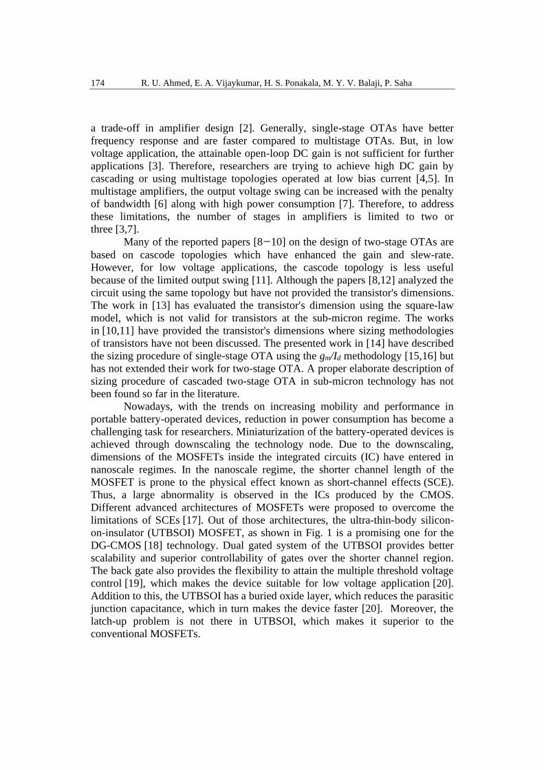
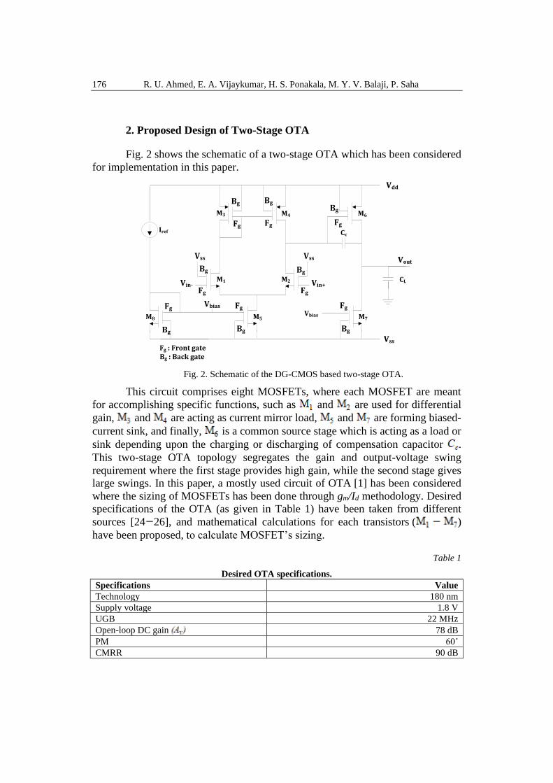
Fig. 2 shows the schematic of a two-stage OTA which has been considered
for implementation in this paper.
Vin- Vin+
Iref Cc
CL
Vdd
Vss
M3 M4
M1 M2
M5M8 M7
M6
Vss
Vbias
Vbias
Fg
Bg
Fg
Bg
Fg
Fg
Bg Bg
Fg
Fg
Bg
Fg
Bg
Fg
Bg
Vss
Bg
Fg : Front gateBg : Back gate
Vout
Fig. 2. Schematic of the DG-CMOS based two-stage OTA.
This circuit comprises eight MOSFETs, where each MOSFET are meant
for accomplishing specific functions, such as and are used for differential
gain, and are acting as current mirror load, and are forming biased-
current sink, and finally, is a common source stage which is acting as a load or
sink depending upon the charging or discharging of compensation capacitor .
This two-stage OTA topology segregates the gain and output-voltage swing
requirement where the first stage provides high gain, while the second stage gives
large swings. In this paper, a mostly used circuit of OTA [1] has been considered
where the sizing of MOSFETs has been done through gm/Id methodology. Desired
specifications of the OTA (as given in Table 1) have been taken from different
sources [24 26], and mathematical calculations for each transistors ( )
have been proposed, to calculate MOSFET’s sizing.
Table 1
Desired OTA specifications.
Specifications Value
Technology 180 nm
Supply voltage 1.8 V
UGB 22 MHz
Open-loop DC gain 78 dB
PM 60˚
CMRR 90 dB
Design of double-gate CMOS based two-stage operational transconductance amplifier using…177
Slew rate 20 V/µs
0.1 V
0.8 V
Reference current 20 µA
Load capacitor 4 pF
An algorithm has been designed to automate the sizing procedure through
MATLAB.
2.1 Compensation Capacitor (Cc)
Simplest frequency compensation technique uses the miller effect by
connecting the across the high gain stages. This consequence in pole-splitting
which enhances the closed-loop stability [27]. The governs the location of
poles and zeros of the amplifier transfer function. To attain 60˚ PM the least
possible value of is [1]:
, (1)
where is the load capacitance. Substituting the value of in (1) gives the
value of 0.88 pF. In this presented work 1 pF is considered.
2.2 Differential Gain Stage
The differential gain stage is comprised of n-channel MOSFETs M1 and
M2, which determines the gain of the first stage and UGB requirement. The
transconductance of M1 and M2 is obtained as follows [1,2]:
. (2)
Equation (2) yields gm1,2 138.2 µS. Since the reference current Iref splits equally
between M1 and M2. So current flowing through them is Id1,2=10 µA and gm/Id of
M1 and M2 is:
. (3)
The desired DC gain considered is 78 dB. This gain is distributed among the two
stages of OTA. The gain of the first stage considered is Av1 40 dB and that of
second stage is Av2 38 dB. The gain of the first stage is given by [1]:
, (4)
which implies gds2+gds4 ≤ 1.38 µS. This inequality is shared equally by M2 and
M4, i.e. gds2=gds4 ≤ 0.69 µS. The intrinsic gain of M1 and M2 is constrained by:
178 R. U. Ahmed, E. A. Vijaykumar, H. S. Ponakala, M. Y. V. Balaji, P. Saha
. (5)
Following the gm/gds vs gm/Id plots for n-channel MOSFETs reported in [22] (for a
parametric sweep of 280 nm: 200 nm: 2.88 μm), at (gm/Id)1,2 14 S/A, the plot
for L1,2 880 nm gives the value (gm/gds)1,2 ≈ 223, which satisfies the requirement
in (5). The channel width is calculated using the Id/W vs gm/Id plot in [22] (for
880 nm). Using the values of (gm/Id)1,2 and L1,2 gives a current density
=2.316 µA/µm, thus the width is given by:
. (6)
2.3 Common Source Stage
The current flowing in the second stage determines the transconductance
of the p-channel MOSFET M6. For 60˚ PM, gm6 can be determined using the
relationship [1]:
. (7)
The value of gm6 is calculated as 1216.16 µS. To achieve slew-rate = 20 V/µs the
current flowing through M6 is kept as Id6 80 µA [28] which yields:
. (8)
The gain of the second stage is given by:
, (9)
which implies gds6+gds7 ≤ 15.20 µS. This inequality splits equally between M6 and
M7, i.e. gds6=gds7 ≤7.6 µS. The intrinsic gain of M6 is constrained by:
. (10)
From the gm/gds vs gm/Id plot for p-channel MOSFETs in [22] (for a parametric
sweep of 230 nm: 100 nm: 1.93 μm), the selected channel length L6 = 630 nm
and from Id/W vs gm/Id plot [22], the value of width is calculated as W6 ≈ 160 µm.
To keep the number of fingers Nf = 1, the maximum value of W6 considered is
50 µm and so L6 is re-calculated using the relation:
. (11)
The relation in (11) yields L6 ≈ 0.196 µm.
Design of double-gate CMOS based two-stage operational transconductance amplifier using…179
2.4 Current Mirror Load
The p-channel MOSFETs M3, M4, and M6 form the load structure of the
two-stage OTA. It is necessary that gm/Id of all these transistors are the same for
perfect matching to avoid offset at the output of the first stage [28].
. (12)
Equation (12) yields gm3,4 = 152.02 µS which results:
. (13)
The intrinsic gain of M3 and M4 is constrained by:
. (14)
From the gm/gds vs gm/Id plots for p-channel MOSFETs in [22] (for a parametric
sweep of 180 nm: 100 nm: 1.98 μm), L3,4 = 880 nm is selected. The (gm/Id)3,4
is also constrained by the ViCM,max. Applying KVL across the series of the branch
(M3 M1 M5) of Fig. 2, the related voltage equation is written as:
. (15)
Since the transistor M1,2 is in saturation, the Vdsat1,2 in (15) is written as:
, (16)
where Vth1,2 is the threshold voltage of M1,2. Substituting Vdsat1,2 in (15):
. (17)
Since Vgs1,2+Vdsat5=Vin(-), the final expression for (15) is obtained as:
. (18)
Substituting Vin(-)=ViCM,max in (18) gives the inequality for ViCM,max that can be
applied before driving the input pair transistors M1 and M2 into the saturation
region.
. (19)
Vth1,2 is extracted from the Vth vs gm/Id plot [22] (for L=880 nm), which is
≈ 0.4915 V. Substituting in (19), the lower bound of Vgs3,4 is found as:
. (20)
By using Vgs vs gm/Id plot [22] (for 880 nm), the valid range of (gm/Id)3,4 due to
ViCM,max specification is found as:
180 R. U. Ahmed, E. A. Vijaykumar, H. S. Ponakala, M. Y. V. Balaji, P. Saha
. (21)
As a compromise, (gm/Id)3,4 = 15 S/A is selected which satisfies both (13) and (21)
with adequate margin. The width of W3,4 is selected from the Id/W vs gm/Id
plot [20], where (Id/W)3,4≈0.3569 µA/µm, thus W3,4 ≈ 29 µm.
Biased-Current Sink
The transistor M5 sinks the current through differential pair. The size of
M5 is constrained by the PSRR, CMRR, and minimum common-mode input
voltage (ViCM,min) requirements. The gm5 is calculated from the PSRR using the
relation [28]:
, (22)
where . Substituting the required value of PSRR from
Table 1 in (22) gives the value gm5=190 µS. The CMRR is given by :
, (23)
where Avdc,CM is the common-mode DC gain. Substituting the data from Table 1 in
the following constraint will give the limit of gds5.
(24)
.
Therefore, the output conductance of M5 must satisfy gds5 ≤ 0.94 µS. The current
flowing through M5 is Id5= 20 µA which yields:
. (25)
The intrinsic gain is constrained by :
. (26)
From the gm/gds vs gm/Id plot for n-channel MOSFETs in [22] (parametric sweep
of 180 nm: 200 nm: 2.98 μm), the selected channel length L5 = 1.18 µm. The
ViCM,min that can be applied before driving the M5 into saturation region is
constrained by:
. (27)
Here, Vgs1,2 0.5898 V (for 880 nm). Substituting the required values in (27),
the constraint on Vdsat5 is written as:
. (28)
Design of double-gate CMOS based two-stage operational transconductance amplifier using…181
By using Vdsat vs gm/Id plot [22] (for 1.18 μm), the valid range of gm/Id due to
the input range specification can be written as:
. (29)
As a compromise, gm/Id 10 S/A is selected which satisfies the requirements (25)
and (29) with adequate margin. The width of M5 is selected from the n-channel
MOSFET current density plot [22], where (Id/W)5 ≈ 4.98 µA/µm, thus
W5 ≈ 4.06 µm. To determine the size of M7, we consider the ratio:
. (30)
Substituting the required values in (30), the aspect ratio for M7 is obtained as
(W/L)7 ≈ 14. Considering L7 1.18 µm, the width for M7 is evaluated as
W7 ≈ 16.24 µm.
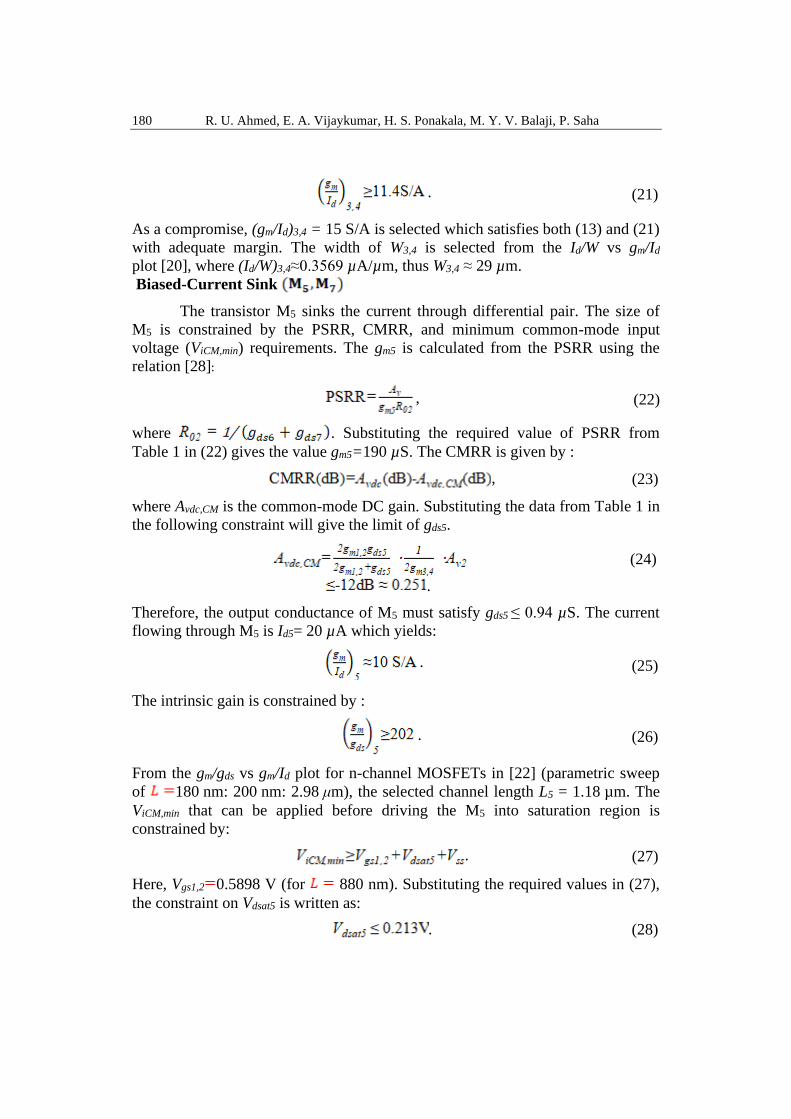
Proposed Algorithm for Sizing Procedure
While designing an analog amplifier, the performance of the circuit is
controlled by the size of MOSFETs. The systematic sizing procedure using gm/Id
methodology has been presented so far evaluates the transistor's dimensions by
solving mathematical equations using data extracted from graphical models.
Regardless of the merit of graphical models, it experiences various drawbacks.
First, it is time taking and has to be repeated many times if there is any change in
the desired specifications. Second, if the circuit fails to achieve the desired
specifications, the sizes have to be re-evaluated. Since the sizing procedure is
structured and can be easily retraced, it fits well to automation. Considerable time
can be saved by automating the sizing procedure. A MATLAB program is written,
where data from graphical models are stored in the form of arrays. For every gm/Id
value in the array, the program finds for the minimum channel length of
transistors which satisfies the desired specifications. The procedure has been
coded as per the flowchart as shown in Fig. 3.
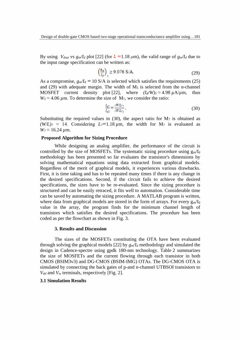
3. Results and Discussion
The sizes of the MOSFETs constituting the OTA have been evaluated
through solving the graphical models [22] by gm/Id methodology and simulated the
design in Cadence-spectre using gpdk 180-nm technology. Table 2 summarizes
the size of MOSFETs and the current flowing through each transistor in both
CMOS (BSIM3v3) and DG-CMOS (BSIM-IMG) OTAs. The DG-CMOS OTA is
simulated by connecting the back gates of p-and n-channel UTBSOI transistors to
Vdd and Vss terminals, respectively [Fig. 2].
3.1 Simulation Results
182 R. U. Ahmed, E. A. Vijaykumar, H. S. Ponakala, M. Y. V. Balaji, P. Saha
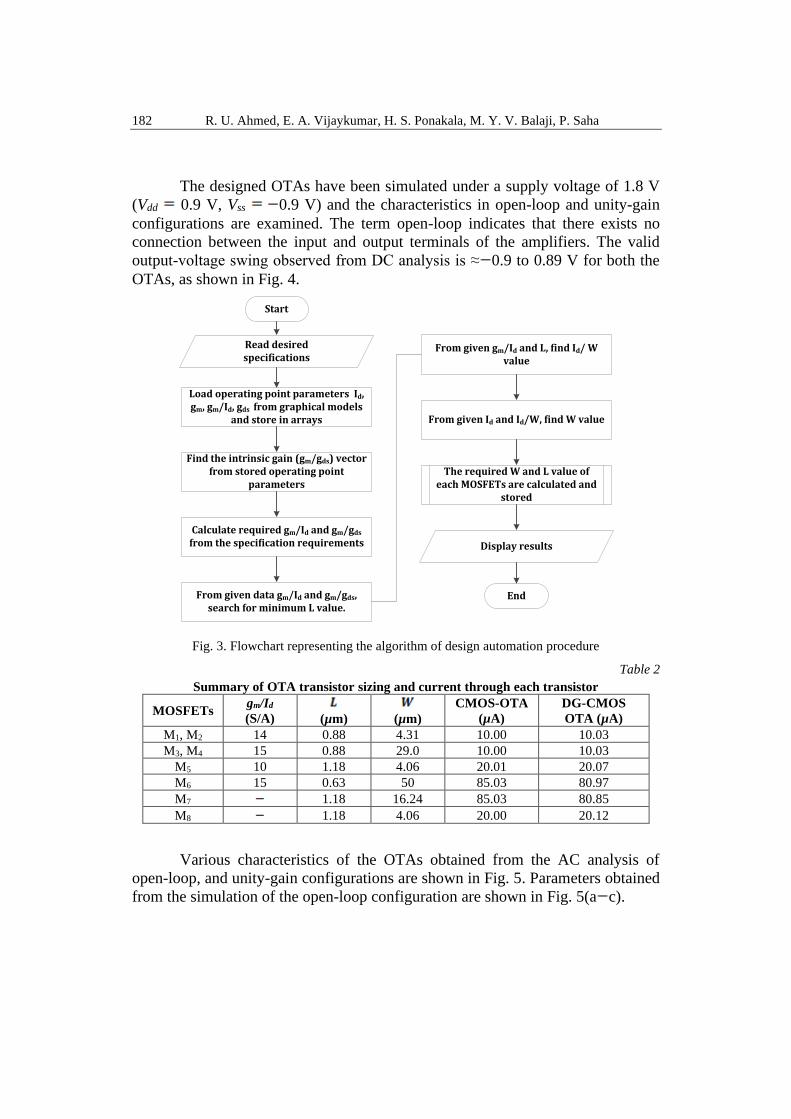
The designed OTAs have been simulated under a supply voltage of 1.8 V
(Vdd 0.9 V, Vss 0.9 V) and the characteristics in open-loop and unity-gain
configurations are examined. The term open-loop indicates that there exists no
connection between the input and output terminals of the amplifiers. The valid
output-voltage swing observed from DC analysis is ≈ 0.9 to 0.89 V for both the
OTAs, as shown in Fig. 4.
Start
Read desired specifications
Load operating point parameters Id, gm, gm/Id, gds from graphical models
and store in arrays
Find the intrinsic gain (gm/gds) vector from stored operating point
parameters
Calculate required gm/Id and gm/gds from the specification requirements
From given Id and Id/W, find W value
The required W and L value of each MOSFETs are calculated and
stored
End
From given gm/Id and L, find Id/ W value
Display results
From given data gm/Id and gm/gds, search for minimum L value.
Fig. 3. Flowchart representing the algorithm of design automation procedure
Table 2
Summary of OTA transistor sizing and current through each transistor
MOSFETs gm/Id
(S/A)
(µm)
(µm)
CMOS-OTA
(µA)
DG-CMOS
OTA (µA)
M1, M2 14 0.88 4.31 10.00 10.03
M3, M4 15 0.88 29.0 10.00 10.03
M5 10 1.18 4.06 20.01 20.07
M6 15 0.63 50 85.03 80.97
M7
1.18 16.24 85.03 80.85
M8
1.18 4.06 20.00 20.12
Various characteristics of the OTAs obtained from the AC analysis of
open-loop, and unity-gain configurations are shown in Fig. 5. Parameters obtained
from the simulation of the open-loop configuration are shown in Fig. 5(a c).
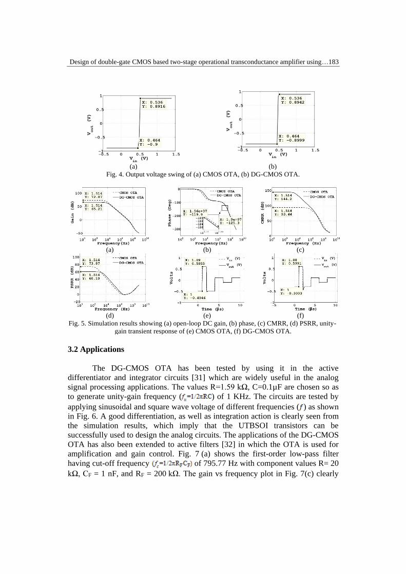
Design of double-gate CMOS based two-stage operational transconductance amplifier using…183
(a) (b)
Fig. 4. Output voltage swing of (a) CMOS OTA, (b) DG-CMOS OTA.
(a) (b) (c)
(d) (e) (f)
Fig. 5. Simulation results showing (a) open-loop DC gain, (b) phase, (c) CMRR, (d) PSRR, unity-
gain transient response of (e) CMOS OTA, (f) DG-CMOS OTA.
3.2 Applications
The DG-CMOS OTA has been tested by using it in the active
differentiator and integrator circuits [31] which are widely useful in the analog
signal processing applications. The values R=1.59 kΩ, C=0.1µF are chosen so as
to generate unity-gain frequency ( ) of 1 KHz. The circuits are tested by
applying sinusoidal and square wave voltage of different frequencies ( ) as shown
in Fig. 6. A good differentiation, as well as integration action is clearly seen from
the simulation results, which imply that the UTBSOI transistors can be
successfully used to design the analog circuits. The applications of the DG-CMOS
OTA has also been extended to active filters [32] in which the OTA is used for
amplification and gain control. Fig. 7 (a) shows the first-order low-pass filter
having cut-off frequency of 795.77 Hz with component values R= 20
kΩ, CF = 1 nF, and RF = 200 kΩ. The gain vs frequency plot in Fig. 7(c) clearly
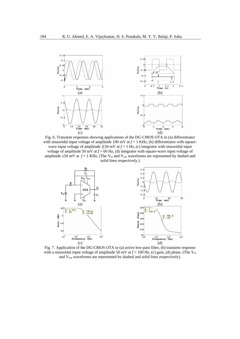
184 R. U. Ahmed, E. A. Vijaykumar, H. S. Ponakala, M. Y. V. Balaji, P. Saha
indicates the property of a low-pass filter with DC gain ≈20 dB which gets
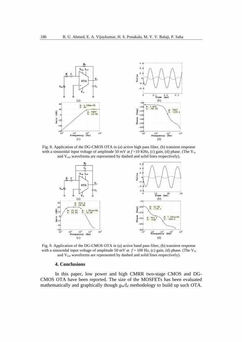
reduced by 3 dB (=16.96 dB) at 795.77 Hz. Fig. 8 (a) show the first-order high-
pass filter designed using the DG-CMOS OTA in which component values
R= 20 kΩ, C= 1 nF, and RF = 200 kΩ are chosen to generate
7957.77 Hz. Similarly, the second-order band-pass filter in Fig. 9(a) is
using the DG-CMOS OTA with component values R= 10 kΩ, C= 1 µF,
CF= 100 pF and RF= 100 kΩ having the low and high cut-
off frequencies of 15.91 Hz and 15.91 KHz respectively. Simulation results of the
active filters [Fig. 7 9] prove the applicability of DG-CMOS OTA in audio
frequency applications. PSRR (dB) 83.2 73.8 60.0
Power (mW) 0.362 0.4 3.72 2.16 1.44 3.8 0.86 0.189 0.181
3.2 Applications
The DG-CMOS OTA has been tested by using it in the active differentiator
and integrator circuits [31] which are widely useful in the analogue signal
processing applications. The values R=1.59 kΩ, C=0.1µF are chosen so as to
generate unity-gain frequency ( ) of 1 KHz. The circuits are tested by
applying sinusoidal and square wave voltage of different frequencies ( ) as shown
in Fig. 6. A good differentiation, as well as integration action is clearly seen from
the simulation results, which imply that the UTBSOI transistors can be
successfully used to design the analogue circuits. The applications of the DG-
CMOS OTA have also been extended to active filters [32], in which the OTA is
used for amplification and gain control. Fig. 7 (a) shows the first-order low-pass.
(a) (b)
(c) (d)
Fig. 6. Transient responses showing applications of the DG-CMOS OTA in (a) differentiator
with sinusoidal input voltage of amplitude 100 mV at f = 1 KHz, (b) differentiator with square-
wave input voltage of amplitude 50 mV at f = 1 Hz, (c) integrator with sinusoidal input
voltage of amplitude 50 mV at f = 60 Hz, (d) integrator with square-wave input voltage of
amplitude ±50 mV at f = 1 KHz. (The Vin and Vout waveforms are represented by dashed and
solid lines respectively.)
(a) (b)
(c) (d)
Fig. 7. Application of the DG-CMOS OTA in (a) active low-pass filter, (b) transient response
with a sinusoidal input voltage of amplitude 50 mV at f = 100 Hz, (c) gain, (d) phase. (The Vin
and Vout waveforms are represented by dashed and solid lines respectively).
Design of double-gate CMOS based two-stage operational transconductance amplifier using…185
The extracted value of DC gain, CMRR, PM and UGB of the CMOS OTA
are 72.8 dB, 93.4 dB, 54.5˚, and 19.0 MHz, respectively. The same parameters for
the DG-CMOS OTA are obtained as 65.2 dB, 114.2 dB, 60˚, and 15.6 MHz,
respectively. Simulation results revealed that the DG-CMOS-OTA has resulted in
high CMRR value (= 144.2 dB). The power consumption is calculated using
the relation: [1], with Id5 and Id6 are current through
M5 and M6, respectively. The parameters such as PSRR, slew-rate, and ViCMR are
extracted from the unity-gain configuration. In this configuration, the OTA draws
a very small current without disturbing the original circuit and has a voltage gain
of unity. Simulation results of the unity-gain configuration are shown in Fig.
5(d f). Slew-rate of both OTAs has been calculated from the unity-gain transient
response, as shown in Fig. 5(e) and (f) which are obtained as 12.11 V/µs and
11.24V/µs for the CMOS and DG-CMOS OTAs respectively. A summary of the
simulation results of the OTAs is listed in Table 3.
Table 3
Performance comparison with prior reported works
Specifications [8] [10] [11] [12] [13] [28] [29] CMOS
OTA
DG-
CMOS
Technology
(nm) 180 180 130 180 180 180 180 180 180
Supply voltage
(V) 1.8 1.2 1.2 1.8 1.8 1.8 1.8 1.8 1.8
Load capacitor
(pF) 1.75 15 1 5.6 5.6 1 5 4 4
UGB (MHz) 160 20 4.8 187 134.2 660 88.9 19.0 15.6
PM (˚) 63 57 80 70.6 73 98.7 54.5 60
DC gain (dB) 74 111 52 83 60.9 80 82.7 72.8 65.2
Slew rate
(V/µs) 26.7 29.5 5 74 94.1 800 8.67 12.19 11.24
ViCM,min (V) 0.07 0
ViCM,max (V) 0.88 0.88
Vout swing 0.9,
0.89
0.9,
0.89
CMRR (dB) 145 127 93.4 144.2
186 R. U. Ahmed, E. A. Vijaykumar, H. S. Ponakala, M. Y. V. Balaji, P. Saha
4. Conclusions
In this paper, low power and high CMRR two-stage CMOS and DG-
CMOS OTA have been reported. The size of the MOSFETs has been evaluated
mathematically and graphically though gm/Id methodology to build up such OTA.
(a) (b)
(c)
(d)
Fig. 8. Application of the DG-CMOS OTA in (a) active high pass filter, (b) transient response
with a sinusoidal input voltage of amplitude 50 mV at f =10 KHz, (c) gain, (d) phase. (The Vin
and Vout waveforms are represented by dashed and solid lines respectively).
(a) (b)
(c)
(d)
Fig. 9. Application of the DG-CMOS OTA in (a) active band pass filter, (b) transient response
with a sinusoidal input voltage of amplitude 50 mV at f = 100 Hz, (c) gain, (d) phase. (The Vin
and Vout waveforms are represented by dashed and solid lines respectively).
Design of double-gate CMOS based two-stage operational transconductance amplifier using…187
A new algorithm has been proposed to verify the MOSFETs sizing. Simulation is
performed in Cadence-spectre where BSIM3v3 and BSIM-IMG models have been
adopted for MOS and UTBSOI devices. The amplifier is able to show optimum
performance, thereby balancing the trade-off between various desired
specifications. Open-loop and unity-gain configurations are simulated accordingly
to show a comparative analysis between the CMOS and DG-CMOS based OTAs.
The CMOS OTA has higher DC gain over the DG-CMOS based OTA, whereas,
from the viewpoint of CMRR and PM, the DG-CMOS OTA is superior to CMOS
OTA. Observation tables offer that in sub-micron regime (180-nm), UTBSOI
transistors can be successfully used to design the analog circuits. Moreover, the
DG-CMOS OTA has been verified by using it in differentiator, integrator, and
active filter circuits which can show the desired output successfully. Since the
process-design kit for the UTBSOI is not available in the existing simulators, so
the layout design of the device is an issue. Thus, ideas for creating the process-
design kit would be a welcoming research topic to improve the results of analog
and mixed-signal circuits further.
Acknowledgments
The authors would like to thank Dr. Shubankar Majumdar, Assistant
professor, and Gudmalwar Ashishkumar Prabhakar, Research scholar from the
Department of Electronics and Communication Engineering, National Institute of
Technology Meghalaya, India for their help and useful suggestions. This work
was supported in part by the National Institute of Technology Meghalaya and in
part by Visvesvaraya PhD Scheme, Government of India.
R E F E R E N C E S
[1]. P.E. Allen, D.R. Holberg, CMOS Analog Circuit Design, 3rd ed. London, UK: Oxford Univ. Press, 2014
[2]. B. Razavi, Design of Analog CMOS Integrated Circuits, 2nd ed. New York: McGraw-Hill, 2001
[3]. H. Aminzadeh, M. Danaie, R. Lotfi, “Design of high-speed two-stage cascode-compensated operational
amplifiers based on settling time and open-loop parameters,” Integr. VLSI J., vol. 41, no. 2, Feb.
2008, pp. 183−192
[4]. F. You, S. Embabi, E. Sanchez-Sinencio, “A multistage amplifier topology with nested gm-c
compensation for low-voltage application,” in Proc. Int. Symp. Solid-State Circuits, San Francisco,
USA, Feb. 1997, pp. 348−349
[5]. H. Veldandi, S.R. Aahmed, “Design procedure for multifinger MOSFET two-stage OTA with shallow
trench isolation effect,” IET Circuits Devices Syst., vol. 12, no. 5, Aug. 2018, pp. 513−522
[6]. R.G.H. Eschauzier, L.P.T. Kerklaan, J.H. Huijsing, “A 100 MHz 100 dB operational amplifier with
multipath nested miller compensation structure,” IEEE J. Solid-State Circuits, vol. 27, no. 12, Dec.
1992, pp. 1709−1717
[7]. K.N. Leung, P.K.T. Mok, “Analysis of multistage amplifier frequency compensation,” IEEE Trans.
Circuits Syst. I: Fundam. Theory Appl., vol. 48, no. 9, Sep. 2001, pp. 1041−1056
[8]. A.P. Perez, Y.B.N Kumar, E. Bonizzoni, F. Maloborti, “Slew-rate and gain enhancement in two stage
operational amplifiers,” in Proc. IEEE Int. Symp. Circuits Syst., Taipei, Taiwan, May 2009, pp.
2485−2488
[9]. R. Nagulapalli et al., “A novel high CMRR trans-impedance instrumentation amplifier for biomedical
applications,” Analog Integr. Circuits Signal Process., vol. 98, no. 2, Feb. 2019, pp. 233−241
188 R. U. Ahmed, E. A. Vijaykumar, H. S. Ponakala, M. Y. V. Balaji, P. Saha
[10]. M. Akbari, O. Hashemipour, “High gain and high CMRR two-stage folded cascode OTA with nested
miller compensation,” J. Circuits, Syst. Comp., vol. 24, no. 4, Jan. 2015, pp. 1550057-(1−13)
[11]. M. Yang, G.W. Roberts, “Synthesis of high gain operational transconductance amplifiers for closed-loop
operation using a generalized controller-based compensation method,” IEEE Trans. Circuits Syst. I:
Reg. Papers, vol. 63, no. 11, , Nov. 2016, pp. 1794−1806
[12]. G.A. Fahmy, R.K. Pokharel, H. Kanaya, K. Yoshida, “Indirect compensation technique based two-stage
recycling folded cascode amplifier for reconfigurable multi-mode sigma-delta ADC,” in Proc. IEEE
Int. Conf. Electron Devices and Solid-State Circuits, Hong Kong, China, Dec. 2010, pp. 1−4
[13]. R.S. Assad, J.S-. Martinez, “The recycling folded cascode: A general enhancement of the folded cascode
amplifier,” IEEE J. Solid-State Circuits, vol. 44, no. 9, Sep. 2009 , pp. 2535−2542
[14]. M.N. Sabri, H. Omran, M. Dessouky, “Systematic design and optimization of operational
transconductance amplifier using gm/ID design methodology,” Microelectronics J., vol. 75, May
2018, pp. 87−96
[15]. F. Silveira, D. Flandre, P.G.A. Jespers, “A gm/ID based methodology for the design of CMOS analog
circuits and its application to the synthesis of a silicon-on-insulator micropower OTA,” IEEE J. Solid-
State Circuits, vol. 31, no. 9, Sep. 1996, pp. 1314−1319
[16]. T. Konishi, K. Inazu, J. G. Lee, M. Natsui, S. Masui, B. Murmann, “Design optimization of high-speed
and low-power operational transconductance amplifier using gm/ID lookup table methodology,”
IEICE Trans. Electron., vol. E94-C, no. 3, Mar. 2011, pp. 334–345
[17]. N. Paydavosi et al., “BSIM - SPICE models enable FinFET and UTB IC designs,” IEEE Access, vol. 1,
May 2013, pp. 201-215
[18]. M. Cheralathan et al., “Implementation of nanoscale double-gate CMOS circuits using compact
advanced transport models,” Microelectronics J., vol. 44, no. 2, Feb. 2013, pp. 80−85
[19]. S. Khandelwal et al., “BSIM-IMG: A compact model for ultrathin-body SOI MOSFETs with back-gate
control,” IEEE Trans. Electron Devices, vol. 59, no. 8, Aug. 2012, pp. 2019−2026
[20]. P.H. Vora, R. Lad., “A review paper on CMOS, SOI and FinFET technology,” DR Industry Articles,
2017, pp. 1-10, [Online]. Available: https://www.design-reuse.com/articles/41330/cmos-soi-finfet-
technology-review-paper.html. [Accessed: 9 December, 2019].
[21]. BSIM-IMG Model. [Online]. Available: http://bsim.berkeley.edu/models/bsimimg/. [Accessed: 10
August, 2017].
[22]. R.U. Ahmed, E.A. Vijaykumar, P.Saha, “Single-Stage Operational Transconductance Amplifier Design
in UTBSOI Technology Based on Methodology,” Electronics, vol. 23, no. 2, Dec. 2019,
pp. 52 59
[23]. W. Liu, C. Hu, “BSIM3v3 MOSFET model,” Int. J. of High-Speed Electron. Syst., vol. 9, no. 3, 1998,
pp. 671−701
[24]. G. Palmisano, G. Palumbo, S. Pennisi, “Design procedures for two stage CMOS OTAs: a tutorial,”
Analog Integr. Circuits Signal Process., vol. 27, no. 3, May 2001, pp. 179−189
[25]. R. Marston, “Understanding and using ‘OTA’ OP-AMP ICs,” Nults Volts Mag., May 2003, pp. 70−74
[26]. Y.M. Qureshi, “Design and layout of two stage high bandwidth operational amplifier,” Int. J. Electron.
Commun. Eng, vol. 6, no. 11, 2012, pp. 1272−1283
[27]. J. Mahattanakul, “Design procedure for two-stage CMOS operational amplifiers employing current
buffer,” IEEE Trans. Circuits Syst. II: Exp. Briefs, vol. 52, no. 11, Nov. 2005, pp. 766−770
[28]. A.J. Rao, “Analog front-end design using the gm/ID method for a pulse-based plasma impedance probe
system,” M.S. thesis, Utah State University, Logan, USA, 2010.
[29]. M.M. Ahmadi, “A new modeling and optimization of gain-boosted cascode amplifier for high-speed and
low-voltage applications,” IEEE Trans. Circuits Syst. II: Exp. Briefs, vol. 53, no. 3, Mar. 2006, pp.
169−173
[30]. A. Mesri, M.M. Pirbazari, K. Hadidi, A. Khoei, “High gain two stage amplifier with positive capacitive
feedback compensation,” IET Circuits Devices Syst., vol. 9, no. 3, May 2015, pp. 181–190
[31]. R.A. Gayakwad, Op-amps and Linear Integrated Circuits, 4th ed. New Delhi, India: PHI., 2010
[32]. S. Franco, Design with Operational Amplifiers and Analog Integrated Circuits, 3rd ed. New York:
McGraw-Hill, 2013
Related Documents