Copyright STARC 2005 <1> Design Methodology toward DFM June 20, 2005 Nobuyuki Nishiguchi Methodology Group, Development Department-1 STARC STARCAD-21 overview This project is supported by Incorporated Administrative Agency NEDO as a part of the Focus 21 program STARC Aids your Design

Welcome message from author
This document is posted to help you gain knowledge. Please leave a comment to let me know what you think about it! Share it to your friends and learn new things together.
Transcript

Copyright STARC 2005 <1>
Design Methodology toward DFMDesign Methodology toward DFM
June 20, 2005 Nobuyuki Nishiguchi
Methodology Group, Development Department-1 STARC
STARCAD-21 overview
This project is supported by IncorporatedAdministrative Agency NEDO as a partof the Focus 21 program
STARC Aids your Design
Copyright STARC 2005 <2>
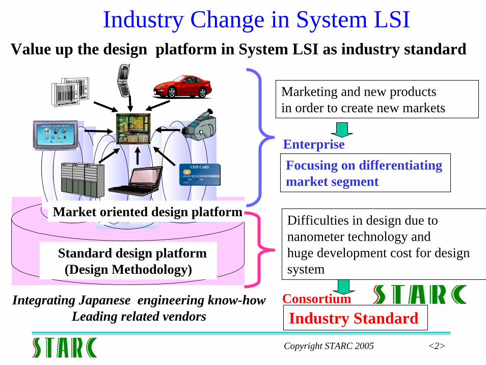
Industry Change in System LSIValue up the design platform in System LSI as industry standard
Industry Standard
Marketing and new productsin order to create new markets
Standard design platform(Design Methodology)
公共分野産業分野
民生分野Market oriented design platform
Focusing on differentiating market segment
Difficulties in design due to nanometer technology andhuge development cost for design system
Consortium
Enterprise
Integrating Japanese engineering know-howLeading related vendors
Copyright STARC 2005 <3>
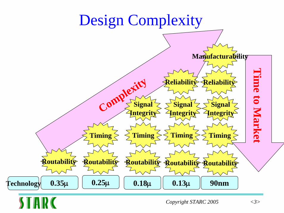
Design Complexity
Complexity
0.35μ 0.25μ 0.18μ 0.13μ
Routability Routability Routability Routability
Timing Timing Timing
SignalIntegrity
Reliability
Technology
Tim
e to Market
90nm
Routability
Timing
Reliability
Manufacturability
SignalIntegrity
SignalIntegrity

Copyright STARC 2005 <4>
Key issues in UDSM phenomenaTiming, Signal Integrity, Reliability and Manufacturability
are NOT independent but trade off
Timing
Signal Integrity
Reliability
Manufacturability
APLL
+-
•Delay estimation•Delay accuracy•Process variation•Variable temperature and voltage•Delay calculation
•Cross talk noise•Cross talk delay•Static IR drop•Dynamic IR drop
•Electron migration•Hot carrier•NBTI
•UDSM design rule•Data density•Antenna effect•Metal slotting
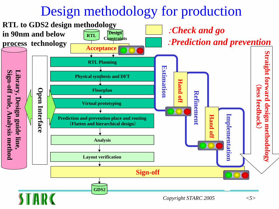
Copyright STARC 2005 <5>
Physical synthesis and DFT
Design methodology for productionRTL
Floorplan
Virtual prototyping
RTL Planning
Prediction and prevention place and routing(Flatten and hierarchical design)
Layout verification
GDS2
Sign-off
Library, D
esign guide line,Sign-off rule, A
nalysis method
Open Interface
Analysis
Estim
ation Refinem
ent
Implem
entation
Hand off
Hand off
:Prediction and prevention:Check and go
Straight forward design m
ethodology
(less feedback
)
RTL to GDS2 design methodology in 90nm and belowprocess technology
Acceptance
DesignConstraints
Copyright STARC 2005 <6>
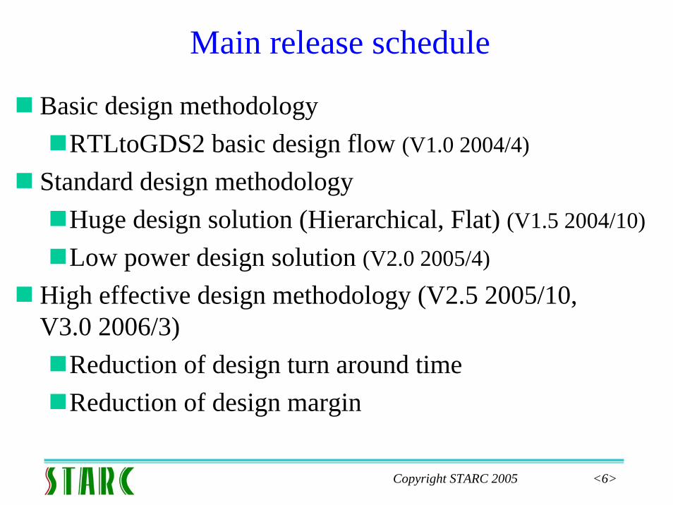
Main release schedule
Basic design methodology RTLtoGDS2 basic design flow (V1.0 2004/4)
Standard design methodology Huge design solution (Hierarchical, Flat) (V1.5 2004/10)
Low power design solution (V2.0 2005/4)
High effective design methodology (V2.5 2005/10,V3.0 2006/3)
Reduction of design turn around timeReduction of design margin
Copyright STARC 2005 <7>
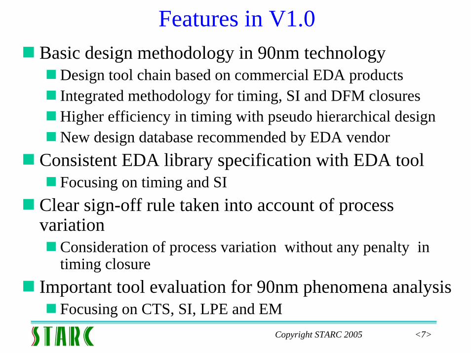
Features in V1.0Basic design methodology in 90nm technology
Design tool chain based on commercial EDA productsIntegrated methodology for timing, SI and DFM closuresHigher efficiency in timing with pseudo hierarchical designNew design database recommended by EDA vendor
Consistent EDA library specification with EDA tool Focusing on timing and SI
Clear sign-off rule taken into account of process variation
Consideration of process variation without any penalty in timing closure
Important tool evaluation for 90nm phenomena analysis Focusing on CTS, SI, LPE and EM

Copyright STARC 2005 <8>
Sign-off check flow
Layout Netlist RTLGolden Data
After antenna and filling metal
LPE
STA
IR-Drop/
Power EM
Layout verification
Formal Verification
Netlist validation
Sim.
Delay
Xtalk noise
Sign-Off check item
Xtalk delay
Signal EM
Max Capacitance./Transition

Copyright STARC 2005 <9>
Inserting double via as DFM
Copyright STARC 2005 <10>
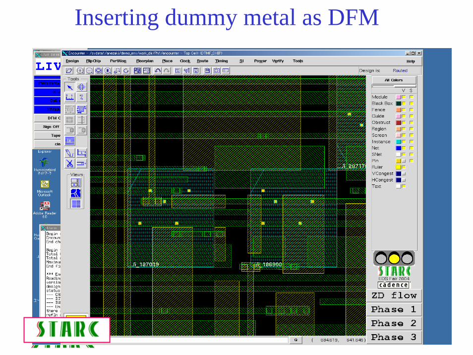
Inserting dummy metal as DFM

Copyright STARC 2005 <11>
BLK3 BLK3 BLK3 BLK3
V1.5 Hierarchical design - Chip image -
BLK1 BLK2
•Push Down •Push Down
•L-shape
Push down for power line
Power supply over the block
Flat region
Block
(Push down)
Push down for signal and buffer
BLK4
TOP
BLK1 BLK2 BLK3 BLK4 ...
Abutment block
Black box block
Repeated block
(without push down)
Copyright STARC 2005 <12>
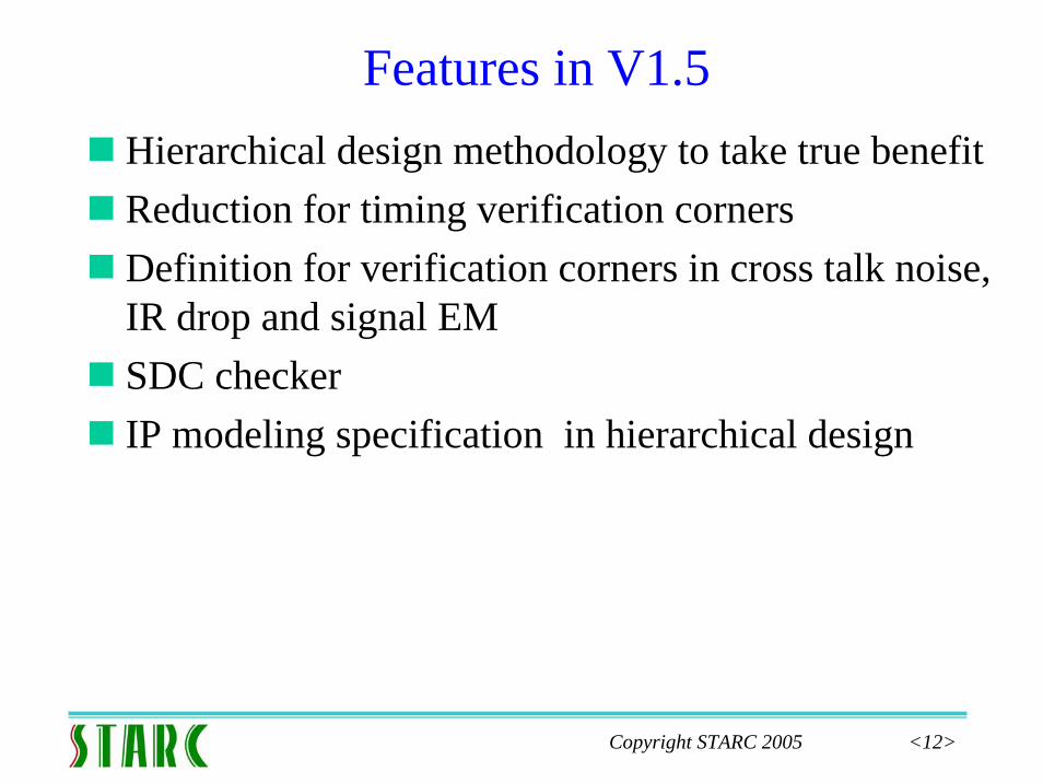
Features in V1.5Hierarchical design methodology to take true benefitReduction for timing verification cornersDefinition for verification corners in cross talk noise, IR drop and signal EMSDC checkerIP modeling specification in hierarchical design

Copyright STARC 2005 <13>
V2.0 Low power design - Chip image -
Island Sleep Mode Voltage
Power 1 ON 1.2V
Power 2 ON/OFF 1.2V
Power 3 ON 1.0V
Currentshut downCircuit
Multi voltage cell
Voltage levelshifter
Power 3island
Gatedclock
Power 1island
Multi Vth for optimizingleak currents
Power optimization
Power 2island (Sleep)
CTS in multi voltage island
CPU

Copyright STARC 2005 <14>
Features in V2.0Low power design
Design flow for multi power with power shut down operationDesign flow for multi VthDesign rule check for multi power(Ex. Power island, Level shifter insertion)
Cross talk analysis in multi power (among different powers)Multi power supply voltage libraries
1.2V and 1.0VDelay calculation and noise analysis
Gated clock with cloning and decloningCTS in multi power
Copyright STARC 2005 <15>
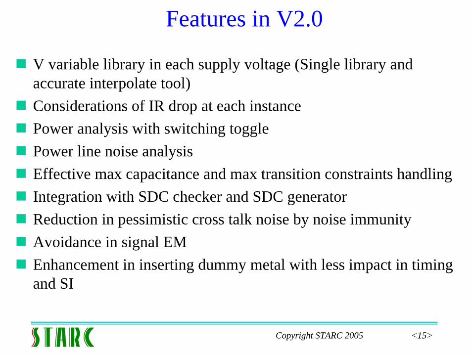
Features in V2.0
V variable library in each supply voltage (Single library and accurate interpolate tool) Considerations of IR drop at each instancePower analysis with switching toggle Power line noise analysisEffective max capacitance and max transition constraints handlingIntegration with SDC checker and SDC generatorReduction in pessimistic cross talk noise by noise immunityAvoidance in signal EM Enhancement in inserting dummy metal with less impact in timing and SI
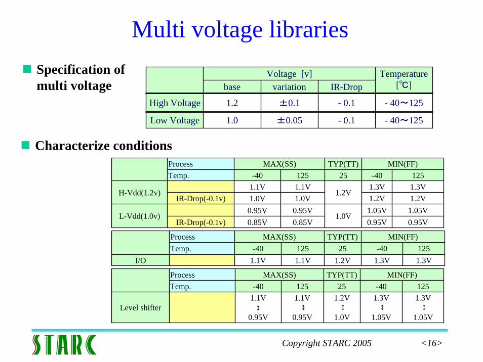
Copyright STARC 2005 <16>
Multi voltage libraries Voltage [v]
base variation IR-Drop
High Voltage 1.2 ±0.1 - 0.1 - 40~125
Low Voltage 1.0 ±0.05 - 0.1 - 40~125
Temperature[℃]
Specification of multi voltage
Characterize conditions
0.95V0.95V0.85V0.85VIR-Drop(-0.1v)1.05V1.05V
1.0V0.95V0.95V
L-Vdd(1.0v)
1.2V1.2V1.0V1.0VIR-Drop(-0.1v)1.3V1.3V
1.2V1.1V1.1V
H-Vdd(1.2v)
125-4025125-40Temp.MIN(FF)TYP(TT)MAX(SS)Process
1.3V1.3V1.2V1.1V1.1VI/O125-4025125-40Temp.
MIN(FF)TYP(TT)MAX(SS)Process
1.3V↕
1.05V
1.3V↕
1.05V
1.2V↕
1.0V
1.1V↕
0.95V
1.1V↕
0.95VLevel shifter
125-4025125-40Temp.MIN(FF)TYP(TT)MAX(SS)Process

Copyright STARC 2005 <17>
Production flow for low power design Phase1: Design
feasibilityRTL ~ Floorplan
Phase2: DesignRefinement
Placement ~ CTS~Optimization
Phase3: Sign-off implementation
Routing ~ SI ~ DFM
RTL Check
Synthesis
Floorplan
Prototyping
Timing ConstrainAdjust Floorplan
Placement
CTS
Timing Optimization
Timing Optimization
Timing Analysis
FloorplanNet list
Routing
Virtual HierarchicalTiming Optimization
Timing informationPlacement /Routing
Partitioning
GDSII
Power structure
Pow
er D
omai
n
Hie
rarc
hica
l st
ruct
ure
階層BLK設計
FLATTEN
S/O検証
階層TOP設計
CHIPレイアウト確定
BLKモデリング
Block Design
Flattening
Sign-off Verification
Chip Design
Final Chip Design
Block Modeling
Block/Chip Block/ChipRTL
Copyright STARC 2005 <18>
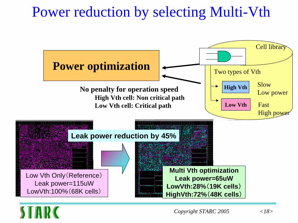
Power reduction by selecting Multi-Vth
Low Vth Only(Reference)Leak power=115uW
LowVth:100%(68K cells)
Leak power reduction by 45%
Multi Vth optimizationLeak power=65uW
LowVth:28%(19K cells)HighVth:72%(48K cells)
Power optimization
High Vth
Low Vth
Cell library
SlowLow power
Two types of Vth
FastHigh power
No penalty for operation speedHigh Vth cell: Non critical pathLow Vth cell: Critical path
Copyright STARC 2005 <19>
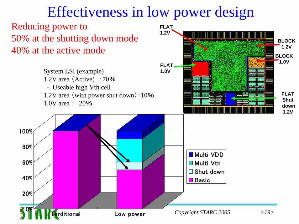
Effectiveness in low power design
System LSI (example)1.2V area (Active) :70%
- Useable high Vth cell1.2V area (with power shut down):10%1.0V area : 20%
Reducing power to50% at the shutting down mode40% at the active mode
0%
20%
40%
60%
80%
100%
Tarditional Low power
Multi VDD
Multi Vth
Shut down
Basic
FLATShutdown1.2V
BLOCK1.2V
FLAT1.0V
BLOCK1.0V
FLAT1.2V

Copyright STARC 2005 <20>
ZD flow Pegas flow
Methodology verification project(SH-4)
First silicon success!!
By using the STARCAD-21 which is fully integrated design methodology•Grantee a chip to work in production on the computer environment at design phase (Sign-off) •Realize similar design turn around time in 90nm to 130nm(33% up in productivity)•Complete solution in 90nm technology difficulty such as timing, signal integrity and design for manufacturing
De-facto standard in SOC design methodology
Copyright STARC 2005 <21>
Beyond V2.0
Reducing design turn around time drasticallyEnhance for timing constraints handling
Multi corners, Multi scenario Golden timing constraint flow
Reducing sign-off cornersTiming and SI
Good hand-off criteriaHierarchical sign-off
Less design margin On-chip variationConsiderations instance base IR-drop more effectivelyTool accuracies
65nm design methodology with DFM

Copyright STARC 2005 <22>
Dela
y C
alc
ula
tion
X-T
alk
Nois
e
X-T
alk
Dela
y
Sta
tic IR
-D
rop
Dynam
ic IR
-D
rop
EM
I
Base N
ois
e
Pow
er E
M
Sig
nal E
M
Hot C
arrie
r
TD
DB
NB
TI
Dynam
ic P
ow
er
Leak P
ow
er
On C
hip
Varia
tion
Inte
r Chip
Varia
tion
Yie
ldin
g
Verific
atio
n C
orn
er
V V
aria
ble
T V
aria
ble
Sta
tistic
al S
TA
LP
E
Anisys tool Methodology
Importance for DFM design factor in 65nm
Higher (Much more engineers need improvement)
Lower (Much more engineers seem tosolve by using similar technique in 90nm)
Comparing with 90nm

Copyright STARC 2005 <23>
Verification with OCV (On-Chip-Variation)What is OCV?
Process variationIncompleteness on OPC(OpticalProximity Correction)Hard consideration in design
Temperature in chipInstance base IR drop
Other design marginsTool accuracy
Current verificationVerification cornerIn order to guarantee chip operationseveral different sets in P: Process (Transistor process )W: Wire (Wire process)V: Voltage (Supply voltage) and T: TemperatureVerifying at each verification corner with OCV for mainly timing
data
clockP: FasterW: TypicalV: LowerT: Typical
P: TypicalW: ThickerV: LowerT: Higher
P: FasterW: More narrowV: TypicalT: Higher
Process variation
No methodology to define OCV value!!

Copyright STARC 2005 <24>
Variation in process and design
Tr size variation
Tr. characteristicvariation
Delayvariation
Signal slew variation
TimingVariation
Gate lengthGate widthOxide thickness
VthIonIoff
Wire widthWire thicknessVia shape
DifferencesIn data and clock
Negative correlation in R and CWidth:Fat → R:decrease C:increaseWidth:Thin → R:increase C: decrease
ht
w
s
Issues in wire
Variation in process Variation in design
Wire shapevariation
Wire characteristicvariation
CapacitanceResistanceVia resistance
setuphold
Cs
Ct Clock)
DFF1 DFF2Q
slew
D(Data)
Process Variation
Copyright STARC 2005 <25>
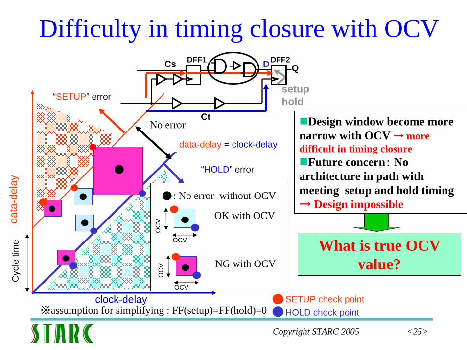
Difficulty in timing closure with OCV
※assumption for simplifying : FF(setup)=FF(hold)=0SETUP check pointHOLD check point
data
-del
ay
clock-delay
“SETUP” error
“HOLD” error
data-delay = clock-delay
No error
Cyc
le ti
me
setuphold
Cs D
Ct
DFF1 DFF2Q
Design window become more narrow with OCV → more difficult in timing closure
Future concern: No architecture in path with meeting setup and hold timing → Design impossible
What is true OCV value?
OK with OCV
NG with OCV
OCV
OC
V
OCV
OC
V
: No error without OCV
Copyright STARC 2005 <26>
Summary
STARCAD-21 is the state of the art design methodology for 90nm and below system LSISTARCD-21 is developed by collection of talent and experience in the Japanese semiconductor industrySTARCAD-21 is applicable to real system LSI nowSTARCAD-21 is the de-facto standard design methodologySTARCD-21 is expanding to support DFM
Related Documents