Design issues in ionized metal physical vapor deposition of copper Michael J. Grapperhaus a) Department of Nuclear Engineering, University of Illinois, 1406 West Green Street, Urbana, Illinois 61801 Zoran Krivokapic b) Advanced Micro Devices, MS 117, 915 De Guigne Drive, Sunnyvale, California 94088-3453 Mark J. Kushner c) Department of Electrical and Computer Engineering, University of Illinois, 1406 West Green Street, Urbana, Illinois 61801 ~Received 7 July 1997; accepted for publication 23 September 1997! The filling of deep vias and trenches with metal for interconnect layers in microelectronic devices requires anisotropic deposition techniques to avoid formation of voids. Ionized metal physical vapor deposition ~IMPVD! is a process which is being developed to address this need. In IMPVD, a magnetron sputter deposition source is augmented with a secondary plasma source with the goal of ionizing a large fraction of the metal atoms. Application of a bias to the substrate results in an anisotropic flux of metal ions for deposition. The ion flux also contributes to ‘‘sputter back’’ of metal deposits on the lip of the via which could lead to void formation. In this article, we describe and present results from a two-dimensional plasma model for IMPVD using a dc magnetron and an inductively coupled auxiliary ionization source. The scaling of copper IMPVD is discussed as a function of buffer gas pressure, sputter source, and source geometry. We show that the deposition rate of metal on the substrate will be reduced as pressure increases due to the increase in diffusive losses. We also show that the sputtering of the auxiliary coils can be a significant issue in IMPVD systems, which must be addressed in tool design. © 1998 American Institute of Physics. @S0021-8979~98!02701-7# I. INTRODUCTION As microelectronic device dimensions continue to shrink, the filling of vias between metalization layers during fabrication of microelectronic devices increasingly requires anisotropic deposition fluxes to prevent void formation. One technique that shows great promise in this regard is ionized metal physical vapor deposition ~IMPVD!. In this system, an auxiliary plasma source is used in conjunction with a sputter deposition source. The goal is to ionize a significant fraction of the sputtered metal atoms prior to their depositing on the substrate. By applying a bias to the substrate to accelerate metal ions, an anisotropic deposition flux can be produced. The substrate bias serves the additional purpose of providing a sputter flux ~either metal ions or buffer gas ions! which competes with deposition, particularly on the lip of the via, and serves to remove encroaching metal atom deposits which could form voids. The IMPVD technique has been developed and demonstrated by Yamashita, 1 and Rossnagel and Hopwood 2–4 for deposition of aluminum and copper. In ex- periments by Rossnagel and Hopwood, the ionized fraction of the aluminum metal atom flux to the substrate was as large as 90%. A zero-dimensional model of IMPVD has been de- veloped by Hopwood and Qian, and provides results which compare favorably with measurements. 5 A schematic of a typical IMPVD system is shown in Fig. 1. The metal source is a dc magnetron. The bias applied to the substrate can be either dc or radio frequency ~rf!. The secondary ionization source is an rf powered inductive coil immersed in the plasma. In neutral metal PVD, the buffer gas pressure is usually only a few mTorr with the intent of having metal atoms traverse the reactor from target to sub- strate having few, if any, collisions. In IMPVD, the buffer gas pressure is somewhat higher ~many mTorr to 10s mTorr! with the intent of slowing the sputtered metal atoms in the buffer gas and providing the opportunity for them to be ion- ized. Unfortunately, this also increases the diffusion losses of metal atoms to surfaces other than the substrate. Experimen- tal scaling studies have shown that, for a constant sputtering rate, the fraction of the metal atoms which are ionized in- creases with increasing buffer gas pressure while the depo- sition rate decreases. 5 In this article, we describe and present results from a two-dimensional model for a copper IMPVD system. We show that the deposition rate of metal on the substrate will be reduced as pressure increases due to the increase in diffusive losses. We also show that the sputtering of the auxiliary coils can be a significant issue in IMPVD systems, which must be addressed in a realistic tool design. The model is described in Sec. II, followed by a discussion of our results for a magne- tron sputter source with rf inductive coils in Sec. III. Our concluding remarks are in Sec. IV. II. DESCRIPTION OF THE MODEL The modeling platform we used in this study was devel- oped at the University of Illinois and is called the hybrid plasma equipment model ~HPEM!. The HPEM has been pre- viously described in detail, 6–9 and so only a brief overview and description of modifications made specifically for this a! Present address: Materials Research Corp., 2120 W. Guadalupe Rd., Gilbert, AZ 85233-2805; electronic mail: [email protected] b! Electronic mail: [email protected] c! Author to whom correspondence should be addressed; electronic mail: [email protected] 35 J. Appl. Phys. 83 (1), 1 January 1998 0021-8979/98/83(1)/35/9/$15.00 © 1998 American Institute of Physics

Welcome message from author
This document is posted to help you gain knowledge. Please leave a comment to let me know what you think about it! Share it to your friends and learn new things together.
Transcript
Design issues in ionized metal physical vapor deposition of copperMichael J. Grapperhausa)
Department of Nuclear Engineering, University of Illinois, 1406 West Green Street, Urbana, Illinois 61801
Zoran Krivokapicb)
Advanced Micro Devices, MS 117, 915 De Guigne Drive, Sunnyvale, California 94088-3453
Mark J. Kushnerc)
Department of Electrical and Computer Engineering, University of Illinois, 1406 West Green Street,Urbana, Illinois 61801
~Received 7 July 1997; accepted for publication 23 September 1997!
The filling of deep vias and trenches with metal for interconnect layers in microelectronic devicesrequires anisotropic deposition techniques to avoid formation of voids. Ionized metal physical vapordeposition~IMPVD! is a process which is being developed to address this need. In IMPVD, amagnetron sputter deposition source is augmented with a secondary plasma source with the goal ofionizing a large fraction of the metal atoms. Application of a bias to the substrate results in ananisotropic flux of metal ions for deposition. The ion flux also contributes to ‘‘sputter back’’ ofmetal deposits on the lip of the via which could lead to void formation. In this article, we describeand present results from a two-dimensional plasma model for IMPVD using a dc magnetron and aninductively coupled auxiliary ionization source. The scaling of copper IMPVD is discussed as afunction of buffer gas pressure, sputter source, and source geometry. We show that the depositionrate of metal on the substrate will be reduced as pressure increases due to the increase in diffusivelosses. We also show that the sputtering of the auxiliary coils can be a significant issue in IMPVDsystems, which must be addressed in tool design. ©1998 American Institute of Physics.@S0021-8979~98!02701-7#
tongrenze
tteiothraedi
iahe
dx-tiorg
deic
g.d
oilferofub-r
hen-s of
en-ringin-po-
ae
l beusiveoilsbed ine-r
el-id-
is
R
ma
I. INTRODUCTION
As microelectronic device dimensions continueshrink, the filling of vias between metalization layers durifabrication of microelectronic devices increasingly requianisotropic deposition fluxes to prevent void formation. Otechnique that shows great promise in this regard is ionimetal physical vapor deposition~IMPVD!. In this system, anauxiliary plasma source is used in conjunction with a spudeposition source. The goal is to ionize a significant fractof the sputtered metal atoms prior to their depositing onsubstrate. By applying a bias to the substrate to accelemetal ions, an anisotropic deposition flux can be producThe substrate bias serves the additional purpose of provia sputter flux~either metal ions or buffer gas ions! whichcompetes with deposition, particularly on the lip of the vand serves to remove encroaching metal atom deposits wcould form voids. The IMPVD technique has been developand demonstrated by Yamashita,1 and Rossnagel anHopwood2–4 for deposition of aluminum and copper. In eperiments by Rossnagel and Hopwood, the ionized fracof the aluminum metal atom flux to the substrate was as laas 90%. A zero-dimensional model of IMPVD has beenveloped by Hopwood and Qian, and provides results whcompare favorably with measurements.5
A schematic of a typical IMPVD system is shown in Fi1. The metal source is a dc magnetron. The bias applie
a!Present address: Materials Research Corp., 2120 W. GuadalupeGilbert, AZ 85233-2805;electronic mail: [email protected]
b!Electronic mail: [email protected]!Author to whom correspondence should be addressed; [email protected]
J. Appl. Phys. 83 (1), 1 January 1998 0021-8979/98/83(1)/35
sed
rnete
d.ng
,ichd
ne-h
to
the substrate can be either dc or radio frequency~rf!. Thesecondary ionization source is an rf powered inductive cimmersed in the plasma. In neutral metal PVD, the bufgas pressure is usually only a few mTorr with the intenthaving metal atoms traverse the reactor from target to sstrate having few, if any, collisions. In IMPVD, the buffegas pressure is somewhat higher~many mTorr to 10s mTorr!with the intent of slowing the sputtered metal atoms in tbuffer gas and providing the opportunity for them to be ioized. Unfortunately, this also increases the diffusion lossemetal atoms to surfaces other than the substrate. Experimtal scaling studies have shown that, for a constant sputterate, the fraction of the metal atoms which are ionizedcreases with increasing buffer gas pressure while the desition rate decreases.5
In this article, we describe and present results fromtwo-dimensional model for a copper IMPVD system. Wshow that the deposition rate of metal on the substrate wilreduced as pressure increases due to the increase in difflosses. We also show that the sputtering of the auxiliary ccan be a significant issue in IMPVD systems, which mustaddressed in a realistic tool design. The model is describeSec. II, followed by a discussion of our results for a magntron sputter source with rf inductive coils in Sec. III. Ouconcluding remarks are in Sec. IV.
II. DESCRIPTION OF THE MODEL
The modeling platform we used in this study was devoped at the University of Illinois and is called the hybrplasma equipment model~HPEM!. The HPEM has been previously described in detail,6–9 and so only a brief overviewand description of modifications made specifically for th
d.,
il:
35/9/$15.00 © 1998 American Institute of Physics

c
h
f
ev
h
h
sati
shcd
c
poglyrt
ere.
earsub-ra-ide
hod
lar
es-
hisitbleer
sec-saryonsheur-
ec-mi-redverseareen-thergyeare
ulk
e-in-lec-is
tionsrce
aveasrip-
ar-to
system will be given here. The base two-dimensional~cylin-drically symmetric! HPEM consists of an electromagnetimodule ~EMM!, an electron Monte Carlo simulation~EMCS!, and a fluid kinetics simulation~FKS!. Inductivelycoupled electric and magnetic fields are computed in tEMM. Those fields are used in the EMCS to generate eletron energy distributions as a function of position and phasThe electron distribution is used to generate source rateselectron impact processes and the electron transport coecients. These parameters are then used in the FKS whmomentum and continuity equations are solved for all heaparticles~neutrals and ions!. A drift diffusion formulation isused for electrons to enable an implicit solution of Poissonequation for the electric potential. A one-dimensional semanalytic sheath model is employed at the plasma-surfaboundary to resolve sheaths which have a thickness less tthe width of a computational cell in the mesh.7 A circuitmodel is employed to provide biases~dc and rf! on poweredsurfaces. The species densities and electrostatic fields pduced by the FKS are transferred to the EMCS and tEMM. This procedure is iterated to a converged solution.
To address the unique conditions of IMPVD systemimprovements to the HPEM have been made for neutral pticle, electron transport, and for defining static magnefields. The improvement in neutral particle transport is thaddition of a neutral atom slowing down Monte Carlo simulation ~NMCS! to account for the long mean free path tranport of hot atoms sputtered from the magnetron target. Timprovement in electron transport included resolving eletron trajectories in regions of high magnetic fields and ading secondary electron emission.
In high magnetic field regions near the magnetron sour(B.1 – 3 kG), the cyclotron frequency is large(.3 – 10 GHz). Resolving the orbits of electrons around thmagnetic fields lines in the EMCS using a simple time steping routine requires that the time step be a small fractionthe cyclotron period. Doing so leads to unacceptably larcomputing time. The gyrokinetic approximation, where onthe guiding center motion of the electron is followed foconditions where the Larmor radius is small compared
FIG. 1. Schematic of reactor modeled in this study.M denotes metal atoms.The magnetron consists of nested loops of magnetic cusps.
36 J. Appl. Phys., Vol. 83, No. 1, 1 January 1998
ec-e.orffi-rey
’si-cean
ro-e
,r-ce--e--
e
e-fe
o
other dimensions, unfortunately cannot be employed hThe gradient in the magnetic field is large~10s kG/cm! andelectrons transition between being highly magnetized nthe sputter source to being weakly magnetized near thestrate. There is a corresponding increase in their Larmordius which violates the gyrokinetic approximation. To avousing a restrictively small time step in the EMCS, the timstepping technique has been modified. Following the metdescribed in Birdsall and Langdon,10 the Lorentz equation isrearranged by defining intermediate velocities,v2 andv1:
v t2Dt/25v22qE'
m
Dt
2~1!
v t1Dt/25v11qE'
m
Dt
2, ~2!
whereE' is the component of the electric field perpendicuto the magnetic field.v2 and v1 are the velocities beforeand after the magnetic field rotation. Putting these exprsions into the finite difference Lorentz equation yields
v12v2
Dt5
q
2m~v11v2!3B ~3!
which can be solved using geometric considerations. Tgives an explicit solution method for updating the implicLorentz equation. This modification increases the allowatime step in the EMCS by a factor of approximately 20 ova direct finite time differencing.
When using biases for either the target or substrate,ondary emission of electrons is an important and necessource of electrons. The secondary emission of electrfrom all surfaces was therefore included in the EMCS. Tprocedure we followed is to launch electrons from the sface of an electrode~or other specified surface! at a ratedetermined by the local ion current to the surface and a sondary electron emission coefficient. When using the seanalytic sheath model, in which the sheath is thin compato electron mean free paths, electrons are assumed to trathe sheath collisionlessly. The electron pseudoparticlestherefore launched perpendicular to the surface with anergy equal to the local sheath potential. When not usingsheath model, electrons are launched with a small ene~typically 4 eV! and a Lambertian angular distribution. Thtrajectories of the secondary electrons and their progenytracked using the same algorithms as in the EMCS for belectrons~or an injected electron beam!11 until they slowbelow a specified energy, typically 3.6 eV~90% of initialenergy!, thereby joining the bulk electrons. The spatially dpendent rate of electrons slowing into the bulk is thencluded as a source term for electrons in the FKS. The etron energy distribution for the secondary electronsseparately computed and used to generate source funcfor electron impact excitation and ionization. These soufunctions are then used in the FKS.
Metal atoms sputtered from the magnetron target han initial energy of a few eV and have a mean free pathlong as a few cm. These characteristics make a fluid desction for their transport questionable. In addition, the dispate energy distribution of the sputtered atoms compared
Grapperhaus, Krivokapic, and Kushner
mneu
ow
thffi
swtroiv
fi-
mgijet
pkdmthraay
ie-lon
tndouiotheioeafab
n-f thh
foatncneom
asiesn-is.ag-rce.a-g’’of
ag-in
orof
esh
-enthera-
ic
heex-forc-r-.ratedheD
mni-theitedflyra--eileper-KSCS,
the bulk metal atoms requires that the influx of metal atobe represented as a separate group. Therefore, a kiMonte Carlo approach, the NMCS, was used to track sptered metal atoms from the surface until they either sldown to thermal speeds or strike a surface~assuming a unitysticking coefficient!. This allows the kinetic effects of theneutrals to be represented during the initial slowing ofsputtered neutrals, while allowing the use of the more ecient fluid equations for the thermal diffusion process.
Sputtered atoms are assumed to be emitted from theface of the target with a cosine angular distribution. Sinceare not resolving the sputter erosion track, the magnesurface is assumed to be planar. The emitted atoms are gan energy specified by Thompson’s law12 which, for incidentions of several hundred eV, can be approximated withsimple cascade distribution,
p~E!52Eb
E2~11Eb /E!3 , ~4!
wherep(E) is the relative probability of emitting an atom oenergyE andEb is the surface binding energy, which typcally ranges from 1 to 4 eV.13
In the NMCS, Monte Carlo particles are launched froeach point along the magnetron target surface with enerand directions selected from these distributions. The tratories of the atoms are then tracked as they move throughplasma region and undergo collisions with the plasma scies. Only momentum transfer collisions with the bacground gas atoms are considered. Collisions are modelehard sphere collisions in the center of mass reference fraThe collision cross section is computed based onLennard–Jones radius of the atoms. For energetic neutthis results in forward peaked scattering. The trajectoriesfollowed until they slow to thermal speeds, or until thestrike a surface. The ending location of the particles is tallto generate a Green’s functionG(r ,r 8) designating the spatial distribution of atoms slowing to thermal speeds at acationr within the plasma volume originating from locatior 8 on the target.
The sputtering rate at each location along the targedetermined by the local ion flux to the surface. In additiocharge exchange reactions near the target surface profast neutrals, which can also sputter target atoms. To accfor sputtering by fast neutrals, all charge exchange reactof ions directed towards the surface which occurs inmesh cell adjacent to the target are assumed to generatneutrals which contribute to sputtering. This approximatwas made based on the fact that these ions have alrtraversed a large fraction of the presheath. Therefore, theneutral flux produced by charge exchange is computedmultiplying the incident ion flux times the neutral atom desity, the charge exchange cross section, and the width olast cell. The total sputter rate is, then, the ion flux to tsurface plus the fast neutral flux times the sputter yield. Tsputter yield is assumed to be constant across the targetgiven incident ion and material composition. The sputter rwhich so computed is then convolved with the Green’s fution for slowing down generated in the NMCS to determithe spatially dependent source rates of sputtered at
J. Appl. Phys., Vol. 83, No. 1, 1 January 1998
stict-
e-
ur-enen
a
esc-hee--ase.els,re
d
-
is,ucent
nsehotndysty
heeer ae-
s
entering the fluid. One can show that in virtually all plasmof interest ~pressures of 10–40 mTorr, electron densit1011– 1012 cm23!, the probability that a sputtered atom udergoes excitation or ionization prior to thermalizingsmall, and so these processes are ignored in the NMCS
Capabilities were also added to compute the static mnetic fields as employed in the magnetron sputter souMagnetrons are typically constructed from lines of permnent magnets. These magnets were represented by ‘‘fillina specified material in the numerical mesh with arrayssmall current loops~current densityj ! oriented in the appro-priate direction to provide the desired orientation of the mnetic field. The current loops then provided source termssolving for vector potential,A, which, by differentiation,yielded the static magnetic fields,
¹31
m¹3A5 j , B5¹3A, ~5!
wherem is the local permeability. We solved for the vectpotential as a boundary value problem using the methodsuccessive over relaxation by extending the numerical mto dimensions twice that shown in Fig. 1, and settingA50on the boundaries.
When using drift-diffusion formulations in the FKS, diffusivities and mobilities for all charged species were thresolved into components parallel and perpendicular tolocal magnetic field. This was accomplished by definingdial and axial mobilities where, for example,
m r5m0
11~qBr /mnm!2
11~qB/mnm!2 , ~6!
wherem r is the mobility for radial transport,m0 is the iso-tropic mobility, Br is the radial component of the magnetfield, B is total magnitude of the field, andnm is the momen-tum transfer collision frequency.
Electron impact cross sections and ion mobilities for tmetal systems of interest are not well characterized. Forample, few electron impact cross sections are availableAl and Ti, which are of particular interest in the semicondutor industry. The knowledge base for Cu is fairly well chaacterized because of past interest in copper vapor lasers14,15
The lack of a complete cross section set and gas phasecoefficients for Al and Ti presents difficulty in modeling, antherefore we have modeled a Cu IMPVD system with tintention of characterizing the general behavior of IMPVsystems.
The complexity of the atomic structure of the Cu atorequires some simplifications in order to reduce the magtude of computations needed. Therefore, within the FKS,excited states of copper are lumped into an effective excstate denoted as Cu* , which has the characteristics oCu@2D5/2#. The higher excited states were not explicittracked within the FKS because of their relatively shortdiative decay time14 and their low rate of excitation compared to the Cu@2D5/2# level. This was done to eliminate thnecessity of tracking several excited states of Cu, whmaintaining the important processes. Several runs wereformed with and without the higher excited states in the Fand the results were essentially the same. Within the EM
37Grapperhaus, Krivokapic, and Kushner

a
ng
-rgamrobynnare
in
c
aodn.
th
e
ac-tod atthe
beoc-
put-heheoned
5
eyingtialthee rfthecave
ined
however, electron impact excitations from the ground st(2S1/2), to the metastable states (2D5/2,2D3/2), resonancestates ~2P1/2 and 2P3/2!, and a pseudostate representihigher levels; and from the metastable Cu* @2D5/2# to theresonance states~2P1/2 and 2P5/2! and pseudostate, are included for the purposes of determining the electron enedistribution functions. Cross sections are essentially the sas those used in Ref. 15, except that the ionization csection from the ground state was from curve fitsCarman,16 based on published data of Sheibner, Hazi, aHenry17 and on unpublished raw data of Sheibner aHazi.18 The electron impact cross sections we usedshown in Fig. 2. Heavy body reaction rates were obtainfrom Ref. 15 and a summary of the Ar/Cu reactions usedshown in Table I.III. PLASMA BEHAVIOR IN AN IONIZED METALSPUTTER DEPOSITION REACTOR
The geometry we used in our simulations is shownFig. 1 and is based on the experiments of Yamashita1 and ofRossnagel and Hopwood.2,3 It consists of a 20-cm-diam dmagnetron sputter source with an applied voltage of2250 Von the target. Due to the limitations of our two-dimensionsimulation, only a circular magnet configuration can be meled. The circular sputter track is defined using cusp magrings above the sputter target. The chamber height is 9 cmtwo turn solenoid, powered at 13.56 MHz, is immersed inplasma and deposits 1 kW of inductively coupled power.~Inall instances, the term ‘‘power deposition’’ refers to the n
FIG. 2. Cu electron impact cross sections.~a! Excitations from the groundstate.~b! Excitations from Cu@2D5/2#, our effective Cu* .
38 J. Appl. Phys., Vol. 83, No. 1, 1 January 1998
te
ye
ss
ddedis
l-etAe
t
power deposited in the plasma through charged particleceleration.! The intended purpose of the solenoid power isionize the sputtered metal atoms. The substrate is biase220 V dc to accelerate ions toward the surface. Due tobiasing of the coils~described below!, ions can obtain suffi-cient energy to sputter the coils, which we assume tomade of copper. Therefore, sputtering of copper atomscurs from both the target and the coils.~Sputtering from thecoils is computationally treated in the same manner as stering from the target. A Green’s function is produced by tNMCS for starting locations of sputtered atoms from tsurface of the coil. When combined with the computed iflux to the coils, we obtain the volumetric source of sputtercopper atoms.! The Ar fill pressure is varied from 15 to 4mTorr. The sputter parameters we used wereEb53.5 eV anda sputter yield52.0.
Since the coils are immersed directly in the plasma, thfunction equivalently to electrodes in an reactive ion etch~RIE! system with respect to biasing of the plasma potenand heating the plasma, and so their electrical coupling toplasma must be considered. As a result, we resolve thcycle in the FKS. The details of this coupling depend onconfiguration of the driving circuitry of the coils, a topiwhich is beyond the scope of the present study. We h
TABLE I. Ar/Cu chemistry.
ReactionaRate coefficient
(cm3 s21) Reference
e1Ar→Ar1e b 19e1Ar→Ar@4s#1e b 20e1Ar→Ar@4p#1e b 20e1Ar→Ar11e1e b 21e1Ar@4s#→Ar11e1e b 22e1Ar1→Ar11e b 23e1Cu→Cu1e b 15e1Cu→Cu@2D5/2#1e b 15e1Cu→Cu@2D3/2#1e b 15e1Cu→Cu@2P1/2#1e b 15e1Cu→Cu@2P3/2#1e b 15e1Cu→Cu@pseudostate#1e b 15e1Cu→Cu11e1e b 16e1Cu@2D5/2#→Cu@2D5/2#1e b 15e1Cu@2D5/2#→Cu@2P1/2#1e b 15e1Cu@2D5/2#→Cu@2P3/2#1e b 15e1Cu@2D5/2#→Cu@pseudostate#1e b 15e1Cu@2D5/2#→Cu11e1e b 15Ar*1Ar*→Ar11Ar1e 5310210 24Cu*1Cu→Cu1Cu 1310212 c
Cu*1Cu*→Cu*1Cu 1310212 c
Ar*1Cu→Ar1Cu11e 5310211 c
Ar*1Cu*→Ar1Cu11e 5310211 c
Ar11Cu→Ar1Cu11e 5310210 c
Ar11Cu*→Ar1Cu11e 5310210 c
Cu11Cu→Cu1Cu1 6310210 c
Ar11Ar→Ar1Ar1 131029 c
aIn the FKS, all excitations of Ar are lumped into Ar* , which is effectiveAr@4s#, and all excitations of Cu are lumped into Cu* , which is effectivelyCu@2D5/2#.
bRate coefficients are calculated from electron energy distribution obtain the EMCS.
cEstimated.
Grapperhaus, Krivokapic, and Kushner

tia
gla
.a
reza
ina-
’ex-
ivenerage
iontion.is-as
andin-rr,rr
on-theivercetronCu
on
eu-tterfaceon
isnse-ak.5
sthe
e
oursr-
therefore simply specified the amplitude of the rf potenthe coils to be 100 V,~200 V peak-to-peak!, which we ac-knowledge to be a lower limit, and that there be a sinblocking capacitor in series with power supply upon whichdc bias is collected. Since the area ratio~coil to wall! is verylarge, the dc bias typically is nearly the rf amplitude.
The electron density and Cu1 density are shown in Fig3, for 35 mTorr Ar fill pressure. The electron density haspeak value of 1.431012 cm23, which is somewhat highethan that obtained in a similar size and powered inductivcoupled etching reactors, and is likely due to the low ionition potential of Cu~7.49 eV!. Although the primary ioniza-tion source for the electrons is near the coils where theductive power deposition peaks, the large aspect ratiolack of volumetric sources of electron loss~such as attachment or dissociative recombination! leads to the electrondensity peaking on axis.~In all instances, the term ‘‘source’refers to the volume production of particular speciespressed as particles/cm3 s.! The source of ions due to electron impact ionization near the coils is 631016 cm23 s21 fora power deposition of 1300 W from capacitive and inductcoupling of the coils. The ionization source near the magtron is 531015 cm23 s21 for an applied magnetron powedeposition of 1700 W. The ionization source near the mnetron is smaller inspite of the higher magnetron pow
FIG. 3. Electron and Cu1 ion density for an IMPVD at 35 mTorr, with2250 V on the sputter target, 1 kW inductive power, and220 V applied tothe substrate.~a! Electron density. Contours values are31011 cm23. ~b!Cu1 ion density. Contours values are31010 cm23. The Cu1 density is'25% of the total ion density.
J. Appl. Phys., Vol. 83, No. 1, 1 January 1998
l
e
ly-
-nd
-
-
-r
deposition because the majority of the power goes intoacceleration across the sheath rather than electron excitaContributions to the ionization source from secondary emsion are displaced into the bulk. The magnetron functionsan externally sustained discharge where ionization,hence current to the target, is largely determined by theductive coil heating. At the operating pressure of 35 mTothe electron collisionality is much higher than at a few mTowhere traditional sputter magnetrons operate. This collisiality somewhat compromises the trapping of electrons inclosed track of the magnetron and produces a diffuscharged density profile, rather than a well confined soubeneath the sputter target. Some scalloping of the elecdensity in the cusps of the magnetron can be seen. The1
density has a peak value of 3.531011 cm23, approximately25% of the total ion density, and has a profile centeredaxis, following the electron density.
The source of sputtered Cu atoms and the total Cu ntral atom density are shown in Fig. 4. The Cu atom spusource is the rate at which atoms sputtered from the surslow down into the thermal group, making the transitifrom kinetic transport to fluid transport. The sputter sourcepeaked near the radial edge of the plasma zone, a coquence of the high rate of sputtering from the coils. The pevalue of the source of sputtered Cu atoms is 131016 cm23 s21. This high rate of sputtering from the coilis sustained by the large amount of power deposition near
FIG. 4. Neutral copper properties.~a! Source of sputtered atoms which havslowed to thermal speed. Contours values are31015 cm23 s21. ~b! Cu neu-tral density, including both ground state and excited state atoms. Contvalues are31011 cm23. The Cu density peaks off axis due to coil sputteing.
39Grapperhaus, Krivokapic, and Kushner
kgtrCl
g-rarctee
o
onumdiisnsobtn
3
ieisctenueoCtlyaltha-s.mmtib
%he-f tth
drgto
omatb
ua
hic
n.
.y,k
e,d-
ng
n
5
,
vicinity of the rf coils. This produces a high ion flux baconto the surface of the coils which, combined with the larsheath potential, produces sputtering. The total Cu neudensity, which includes ground state and excited stateatoms, is shown in Fig. 4~b!. The peak value for the neutraCu is 2.031012 cm23 and is peaked off axis below the manets. The off axis peak is caused by the high sputteringfrom the coils as well as by the off axis sputtering soufrom the target. Due to the fact that the lowest excited staof Cu are metastable yet have a large excitation rate dutheir low threshold energy~1.4 eV!, a large fraction of theCu atoms are excited, in this case approximately 25%.
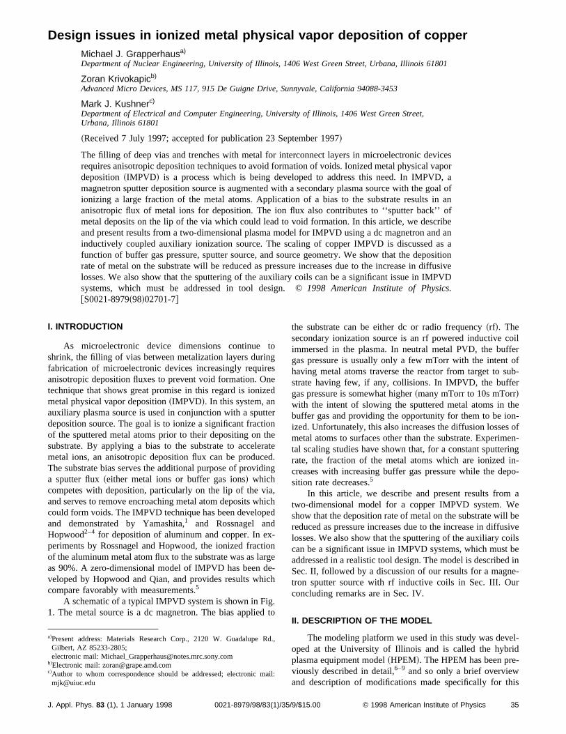
The importance of sputtering of the coil as a sourcemetal atoms has recently been confirmed in experimentsWang et al.25 In these experiments, a Cu dc magnetrsource was used in an IMPVD reactor having alumincoils. Optical emission from excited Cu and Al states incated comparable densities of each metal. Surface analysthe resulting film showed that, depending on conditiocomparable fractions of aluminum and copper weretained. It has also been reported that the uniformity of meatom deposition is a function of inductive power depositioan effect attributed to coil sputtering.26
The fluxes of Cu species to the wafer surface formTorr Ar fill pressure are shown in Fig. 5~a! while includingsputtering from the coil and assuming that all Cu spechave a unity sticking coefficient. The unthermalized fluxthe flux of sputtered atoms which have traversed the reafrom the target to the substrate without undergoing sufficicollisions to slow to thermal speeds. The unthermalized flis strongly peaked at the outer edge of the wafer becausthe high rate of sputtering from the nearby coils and theaxis circular sputter track on the target. The thermalizedneutral flux has much less variation although it is slighpeaked at'7.5 cm from the axis. The more uniform thermCu flux compared to the unthermalized flux is due todiffusivity of Cu atoms in the plasma. The ion flux is reltively uniform at small radii, but tapers off at larger radiuFrom experience with designing conventional ICP plassources, one can recoup some of this uniformity by a cobination of operating with a somewhat squatter aspect rawhose value is a sensitive function of pressure, andchanging the position of the rf coils. The flux of the Cu* isrelatively uniform across the wafer and approximately 13of the total. The total deposition flux of Cu is the sum of tfluxes of all neutral~thermal and hot! and ionized Cu species. The total flux increases at larger radius because ounthermalized neutral component, although the flux ofother components are decreasing.
The fraction of the Cu flux to the wafer which is ionizeis '50% near the center of the wafer. It decreases at laradii due to the increase in the unthermalized componenthe neutral flux produced by the proximity of the coils. Tprevent this trend, one must either minimize sputtering frthe coil, place the coils sufficiently far from the wafer ththe sputtered atom flux has opportunity to thermalize andionized prior to striking the substrate, or place the coils oside the chamber. The coils can be placed outside the chber by using an appropriately designed Faraday shield w
40 J. Appl. Phys., Vol. 83, No. 1, 1 January 1998
ealu
teesto
fby
-of,-
al,
5
s
ortxof
ffu
e
a-
o,y
hee
erof
et-m-h
is not electrically shorted by depositing metal atoms.27
The same conditions were simulated with the exceptiothat we specified that there be no sputtering from the coilsThe electron density and Cu1 densities for this case areshown in Fig. 6. The Cu1 density has a peak value of 1.131011 cm23, which is significantly smaller and morestrongly peaked on axis than in the case with coil sputteringThis trend is due to a decrease in neutral copper densitespecially near the coils. The electron density has a peavalue of 1.231012 cm23, slightly smaller than that when in-cluding coil sputtering, however it is more spatially uniformdue to a more uniform ionization rate. Although Cu is moreeasily ionized than Ar, it also has a larger rate of momentumtransfer and a larger rate of inelastic energy loss. Thereforan increase in copper density, in this case caused by incluing sputtering from the coils, results in more cooling of elec-trons by collisions with copper atoms. This results in theelectron temperature being more peaked near the heatisource at the coils.
The copper sputter source and neutral density are showin Fig. 7 for the case where no sputtering is allowed from thecoils. The sputter source has a peak value of 5.31015 cm23 s21 which is smaller than the case where sput-tering is allowed from the coils.~The total sputter rate for a
FIG. 5. Cu deposition flux to the substrate and fraction of the flux which isionized. The neutral flux consists of contributions from Cu ground stateCu* , and the unthermalized sputter flux.~a! Fluxes with sputtering from thecoils. ~b! Fluxes without sputtering from the coils. Coil sputtering producesan off axis maximum in the Cu atom flux.
Grapperhaus, Krivokapic, and Kushner

dethtrn
eddthecao
arctnydi
alu-
hethre
wsceoiilsis
of
henishure
hetheem.o-
gengra-s
s de-wnon-he
ureichredition
ning
toursd
in
fixed sputter yield, which has been assumed in this modepends only on the total flux of ions to the surface. Incase where sputtering from the coils is allowed, the conbutions from the coils actually exceeds the contributiofrom the target.! The peak in the sputter source is locatbelow the magnetron target, although it is not locatedrectly beneath the magnets. This condition results fromrelatively uniform sputter source from the target, combinwith the short mean free path of the neutrals in a cylindrigeometry, leading to a source peaked on axis. Sincesimulation is only two-dimensional, the magnetron tracksat best nested circular loops. Sputtering is therefore direproportional to the ion flux incident onto the target. In macommercial magnetrons, the ‘‘racetrack’’ cuts across rathereby ‘‘mixing’’ incident ion fluxes from different radii.The total neutral Cu density in the plasma has a peak vof 4.631011 cm23. The Cu density for this case is significantly lower and more sharply peaked on axis than wsputtering from the coils is allowed, thereby emphasizingimportance of considering this source of metal atoms inactor design.
The deposition fluxes as a function of radius are shoin Fig. 5~b! when no sputtering is allowed from the coils. Aexpected, all incident fluxes fall off at larger radius, sinthere is no secondary source of sputtered Cu from the cThe overall deposition flux without sputtering from the cois significantly lower than when sputtering from the coils
FIG. 6. Electron and Cu1 ion density without sputtering from the coils.~a!Electron density. Contours values are31011 cm23. ~b! Cu1 ion density.Contours values are31010 cm23.
J. Appl. Phys., Vol. 83, No. 1, 1 January 1998
l,ei-s
i-e
dlurely
i,
e
ne-
n
ls.
allowed, which in turn leads to a slightly higher percentthe flux which is ionized,'60% on axis. This results fromthere being less cooling of the electrons in the plasma wthe Cu density is low. The unthermalized flux in this caseonly a small fraction of the total flux to the surface, whicindicates that the combination of reactor height and pressfor this case provides for sufficient thermalization of tsputtered atoms in the plasma volume, provided thatsputter target is the primary source of copper in the syst
The variations of the Cu ionized fraction and total depsition flux to the wafer with fill pressure and target voltaare shown in Fig. 8. To offset the influence of sputterifrom the coils, values are averaged over the inner 4 cmdius of the wafer, as shown by the vertical line in Fig. 5. Athe pressure increases, the mean free path of the atomcreases. The fraction of sputtered atoms which slow dointo the plasma increases, allowing more of them to be iized before reaching the wafer. The ionized fraction of tflux to the wafer increases from'29% at 15 mTorr to'47% at 45 mTorr. At the same time, increasing presshas the effect of dispersing the atoms due to diffusion, whresults in a lower deposition rate, since more of the sputteatoms are lost to other surfaces in the reactor. The deposflux decreases from'5.531016 cm22 s21 (3900 Å/min) at15 mTorr to '1.531016 cm22 s21 (1100 Å/min) at 45mTorr. This implies a trade off between ionized flux fractioand deposition rate, which for this geometry and operat
FIG. 7. Cu sputter source and density without sputtering from the coils.~a!Source of sputtered atoms which have slowed to thermal speeds. Convalues are31015 cm23 s21. ~b! Cu neutral density, including both grounstate and excited state atoms. Contours values are31011 cm23. The ab-sence of copper sputtering rom the coils results in an on axis maximumCu density.
41Grapperhaus, Krivokapic, and Kushner

uss5r a20
ux
t,ttr
iti
thw
rasin
is-
erhd
innse
o.tal
ni-of
ger.ad
-d tou
es-ofmsheffu--
cha-onntedoms.hen-er-ils
refulrs
F.-
uc-ion
ed
-d.
he
conditions would be between 25 and 35 mTorr. This resagrees qualitatively with the ionized Al experiments of Ronagel and Hopwood.2,3 Experiments by Yamashita with acm gap between the target and the substrate, at 10 mTor800 W dc target power produced a deposition rate of 11Å/min for Cu deposition.1
The variations of Cu deposition flux and the ionized flfraction with target voltage is shown in Fig. 8~b!. In thesecases, the sputter yield was assumed to remain constanthat the main effect of increasing the target voltage isincrease the rate of plasma generation near the magnesurface due to secondary electron emission. The deposflux does not change appreciably between the2100 and the2250 V cases, which implies that at this operating pointion flux to the target is roughly the same between the tcases. As the voltage is increased to2350 V, the depositionrate experiences a small increase due to a slightly largerof ionization by secondary electrons leading to larger rateCu sputtering, although the ionized flux fraction remanear 50%.
By moving the coils further away from the substrate, itexpected that uniformity of the Cu flux will improve by reducing the unthermalized Cu flux resulting from coil sputting. This is shown in Fig. 9, Cu fluxes are plotted when tcoils have been raised 1.5 cm towards the target comparethe standard case. The Cu1 flux is nearly the same as seenthe standard case@Fig. 5~a!#. The main difference betweethis case and the standard case is that the neutral fluxesmaller. The unthermalized flux is substantially reduced,
FIG. 8. Cu deposition flux and fraction of the flux which is ionized~a! as afunction of pressure and~b! as a function of dc voltage on the target. Increasing pressure reduces the Cu flux but increases the fraction ionize
42 J. Appl. Phys., Vol. 83, No. 1, 1 January 1998
lt-
nd0
sooonon
eo
teofs
-eto
ares-
pecially at the outer radius, with a peak value of'1.231016 cm22 s21 ~850 Å/min! at the outer radius compared t'2.831016 cm22 s21 ~2000 Å/min! in the standard caseThe other neutral fluxes are also smaller resulting in a todeposition flux which is smaller, and somewhat more uform. Since the coils have been moved closer to the topthe reactor, diffusion losses of sputtered Cu atoms are larAs the ionized flux is nearly the same, these conditions leto a higher ionized percentage,'62% on the axis.
IV. CONCLUDING REMARKS
A two-dimensional model for ionized metal physical vapor deposition has been developed, and has been appliethe investigation and design of deposition devices for Cdeposition. For a modified magnetron sputter source, prsure plays an important part in determining the transportsputtered atoms. At low pressure, the sputtered atotraverse the reactor with few collisions before reaching twafer, while at higher pressure, the transport becomes disive, which allows for ionization for the metal atoms. However, the increase in pressure creates a diffusive loss menism for atoms to the walls, which reduces the depositirate. Sputtering from the coils is seen to be a significasource of metal atoms. Sputtering from the coils is producby the high plasma density generated near the coils frinductive heating followed by ion acceleration into the coilThis source of metal atoms must also be considered woptimizing the uniformity of the deposition flux to the substrate. Sputtering from the coils may limit the lifetime of thcoils, however the total erosion rate will ultimately be detemined by the difference between deposition onto the coand sputtering. These results emphasize the need for cachoice of coil location, coil material, and circuit parameteto optimize operation.
ACKNOWLEDGMENTS
The authors would like to thank R. J. Carman, K.Sheibner, and A. U. Hazi for their help with the Cu ionization cross section. This work supported by the Semicondtor Research Corporation, National Science Foundat~Grant No. ECS 94-04133, CTS 94-12565!, Office of NavalResearch~Grant No. N00014-94-1-0819!, and the Universityof Wisconsin Engineering Research Center for Plasma AidManufacturing.
FIG. 9. Deposition fluxes and fraction of the flux which is ionized when tcoils are raised 1.5 cm toward the sputter target.
Grapperhaus, Krivokapic, and Kushner
ry,
ec
-
A
ro
19
andber
isco,
363
1M. Yamashita, J. Vac. Sci. Technol. A7, 151 ~1989!.2S. M. Rossnagel and J. Hopwood, Appl. Phys. Lett.63, 3285~1993!.3S. M. Rossnagel and J. Hopwood, J. Vac. Sci. Technol. B12, 449~1994!.4S. M. Gorbatkin, D. B. Poker, R. L. Rhoades, C. Doughty, L. A. Berand S. M. Rossnagel, J. Vac. Sci. Technol. B14, 1853~1996!.
5J. Hopwood and F. Qian, J. Appl. Phys.78, 758 ~1995!.6S. Rauf and M. J. Kushner, J. Appl. Phys.81, 5966~1997!.7M. Grapperhaus and M. J. Kushner, J. Appl. Phys.81, 569 ~1997!.8W. Z. Collison and M. J. Kushner, Appl. Phys. Lett.68, 903 ~1996!.9P. L. G. Ventzek, M. Grapperhaus, and M. J. Kushner, J. Vac. Sci. Tnol. B 12, 3118~1994!.
10C. K. Birdsall and A. B. Langdon,Plasma Physics Via Computer Simulation ~McGraw–Hill, New York, 1985!.
11M. J. Kushner, W. Z. Collison, and D. N. Ruzic, J. Vac. Sci. Technol.14, 2094~1996!.
12T. Heberlein, G. Krautheim, and W. Wuttke, Vacuum42, 47 ~1991!.13M. A. Lieberman and A. J. Lichtenberg,Principles of Plasma Discharges
and Materials Processing~Wiley, New York, 1994!.14R. J. Carman, D. J. W. Brown, and J. A. Piper, IEEE J. Quantum Elect
30, 1876~1994!.15M. J. Kushner and B. E. Warner, J. Appl. Phys.54, 2970~1983!.
J. Appl. Phys., Vol. 83, No. 1, 1 January 1998
h-
n.
16R. J. Carman~private communication!.17K. F. Sheibner, A. U. Hazi, and R. J. W. Henry, Phys. Rev. A35, 4869
~1987!.18K. F. Sheibner and A. U. Hazi~private communication!.19M. Hayashi, Nagoya Institute of Technology Report No. IPPJ-AM-
~1991!.20K. Tachibana, Phys. Rev. A34, 1007~1987!.21D. Rapp and P. Englander-Golden, J. Chem. Phys.43, 1464~1965!.22R. H. McFarland and J. D. Kinney, Phys. Rev.137, A1058 ~1965!.23M. Mitchner and C. Kruger,Partially Ionized Gases~Wiley, New York,
1973!, Chap. 2.24P. K. Leichner and R. J. Ericson, Phys. Rev. A9, 251 ~1974!.25W. W. Wang, J. E. Foster, M. Grapperhaus, A. E. Wendt, J. Booske,
M. J. Kushner, Division of Plasma Physics Annual Meeting, Novem1997 ~unpublished!.
26P. Gopalraja, Y. Tanaka, K. Tanimoto, J. Forster, and Z. Xu,IonizedPhysical Vapor Deposition of Titanium and Titanium Nitride, Paper K1.7~Materials Research Society Sprint 1997 Symposium, San Franc1997!.
27R. Bayer, A. D. Lantsman, and J. A. Seirmarco, US Patent 5,569,~October 1996!.
43Grapperhaus, Krivokapic, and Kushner
Related Documents