Design Insights from Electromagnetic Analysis of Interconnects Yuriy Shlepnev, Simberian Inc. [email protected] Front Range Signal Integrity Seminar, Longmont, CO October 3, 2013 10/8/2013 © 2013 Simberian Inc. 1

Welcome message from author
This document is posted to help you gain knowledge. Please leave a comment to let me know what you think about it! Share it to your friends and learn new things together.
Transcript

Design Insights from Electromagnetic Analysis of
Interconnects
Yuriy Shlepnev, Simberian Inc. [email protected]
Front Range Signal Integrity Seminar, Longmont, CO
October 3, 2013
10/8/2013 © 2013 Simberian Inc. 1

Property rights disclosure
10/8/2013 © 2013 Simberian Inc. 2
Copyright © 2013 by Simberian Inc., All rights reserved. THIS DOCUMENT IS CONFIDENTIAL AND
PROPRIETARY TO SIMBERIAN INC. AND MAY NOT BE REPRODUCED, PUBLISHED OR DISCLOSED TO OTHERS WITHOUT PERMISSION OF SIMBERIAN INC.
Simberian® and Simbeor® are registered trademarks of Simberian Inc. Other product and company names mentioned in this
presentation may be the trademarks of their respective owners.

Outline Introduction Decompositional electromagnetic analysis Broadband material models
Dielectric and roughness models and model identification Nickel model in ENIG plated traces
Modeling discontinuities Planar transitions - control of impedance and skew Vertical transitions – localization and crosstalk
Conclusion References and contacts
10/8/2013 © 2013 Simberian Inc. 3

Introduction Data links running at bitrates 10-30 Gbps and beyond are becoming the mainstream
in the communication and other electronic systems Why is design of PCB and packaging interconnects for such systems is a challenging
problem? It requires electromagnetic analysis over extremely broad frequency bandwidth from DC to 20-50 GHz No frequency-continuous dielectric models available from laminate manufactures No roughness models available from manufacturers Boards are routed in old-style ways based on rules and approximate models and not on EM analysis Boards are not manufactured as designed – large variations and manipulations by manufacturer
Is it possible to design and build interconnects and have acceptable analysis to measurement correlation from DC to 20-50 GHz systematically? Obviously yes, but only if some conditions are satisfied The conditions are partially covered here and discussed in detail in my tutorial at DesignCon 2013 and in
paper presented at EMC 2013 symposium (both available at www.simberian.com) This presentation provides practical examples illustrating how to make decisions on the base of EM analysis Some examples may look counter-intuitive
10/8/2013 © 2013 Simberian Inc. 4

10/8/2013 5
Decompositional analysis of a channel
Chip T-Line Segments
Local Chip Transitions
I/O
Bu
ffer M
od
el
Package T-Line Segments
Local Package Transitions
PCB T-Line Segments
Local PCB Transitions
Local PCB Transitions
Package T-Line Segments
Local Package Transitions
Chip T-Line Segments
Local Chip Transitions
I/O
Bu
ffer M
od
el
Transmission lines (may be coupled) and via-holes, connectors, bond-wires, bumps and ball transitions
Connection of MULTIPORTS
Elements of decompositional analysis that correlates with measurements: 1) Quality of all S-parameter models
2) Broadband material models
3) Possibility of simulation in isolation (localization, de-embedding)
4) Correlation of measurements on manufactured board with the models (benchmarking)
© 2013 Simberian Inc.

Quality of S-parameter models Multiports are usually described with S-parameter models
Produced by circuit or electromagnetic simulators, VNAs and TDNAs in forms of Touchstone or BB SPICE models
Very often such models have issues and may be not suitable for consistent frequency and time domain analyses Not sufficient bandwidth and sampling Passivity, reciprocity and causality conditions may be violated
How to make sure that a model is suitable for analysis? The answer is one of the key elements for design success To make the decision easier, Passivity, Reciprocity and Causality quality metrics
has been introduced in 2010 and implemented in Simbeor software See references on quality of S-parameters at the end of presentation
All models for this presentation are created with Simbeor software Adaptively sampled, reciprocal, passive and causal With bandwidth 50 GHz for 30 Gbps, 16 ps rise time
10/8/2013 © 2013 Simberian Inc.
6

Broadband material models The largest part of interconnects are transmission line
segments Models for transmission lines are usually constructed
with a quasi-static or electromagnetic field solvers T-lines with homogeneous dielectrics (strip lines) can be effectively
analysed with quasi-static field solvers T-lines with inhomogeneous dielectric may require analysis with a full-
wave solver to account for the high-frequency dispersion
Accuracy of transmission line models is mostly defined by availability of broadband dielectric and conductor roughness models
This is the most important elements for design success
10/8/2013 © 2013 Simberian Inc. 7

Causal dielectric models for PCB and PKG Multi-pole Debye-Lorentz (real and complex poles)
Wideband Debye (Djordjevic-Sarkar)
Models for dielectric mixtures (Wiener, Maxwell-Garnet, …)
Models for anisotropic dielectrics (separate definition of Z, and XY-plane components of permittivity tensor)
10/8/2013 © 2013 Simberian Inc. 8
( )2
2 21 1
( )1 2
2
N Kn k k
kn kk
n
frf fi fr i f ffr
ε εε ε δπ
= =
∆ ∆ ⋅= ∞ + +
+ + ⋅ ⋅ −∑ ∑
2
12 1
10( ) ( ) ln( ) ln(10) 10
mrd
r miff
m m ifεε ε
+= ∞ + ⋅ − ⋅ +
Requires specification of value at infinity and poles/residues/damping or DK and LT at multiple frequency points
Continuous-spectrum model Requires specification of DK and LT at one frequency point
Parameters of the causal models are not available from manufacturers!

Causal roughness models
Modified Hammerstad (red), Simbeor (black) and Huray’s snowball (blue) models (RTF/TWS foil example)
Causal if correction is applied to conductor surface
impedance operator Where to get the model parameters?
SR (delta) and RF for Simbeor and MHCC Number of balls, ball size and tile area for Huray’s model
10/8/2013 © 2013 Simberian Inc. 9
See references in the papers (Shlepnev, EMC2012 and DC2012)
( )1 tanh 0.56 1rsK RFδ∆ = + ⋅ −
2 2
241 1
2rhuhex
N rKA r rπ δ δ ⋅ ⋅= + + + ⋅
( )221 arctan 1.4 1rhK RF
π δ
∆ = + ⋅ ⋅ −

10/8/2013 © 2013 Simberian Inc.
10
Material parameters identification with generalized modal S-parameters (GMS-parameters)
Can be used to identify both dielectric and conductor roughness models
Simberian’s patents pending #13/009,541 and #14/045,392
Optimization loop – red line; Automated in Simbeor software

Board for material models identification example
10/8/2013 © 2012 Simberian Inc.
10.5-11 mil wide strip lines, Use measured S-parameters for 2 segments ( 2 inch and 8 inch)
CMP-28 validation board designed and investigated by Wild River Technology http://wildrivertech.com/
11
From Isola FR408 specifications

Measured S-parameters for 2 and 8 inch segments
10/8/2013 © 2013 Simberian Inc.
12
Excellent measurements quality! Original “reflective”
S-parameters
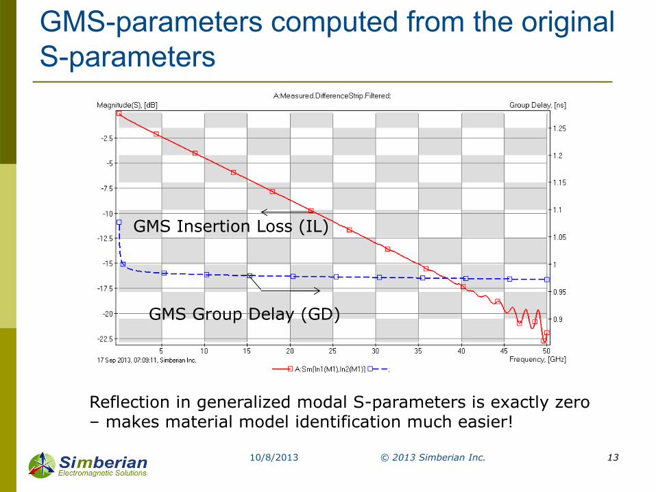
GMS-parameters computed from the original S-parameters
10/8/2013 © 2013 Simberian Inc.
13
GMS Insertion Loss (IL)
GMS Group Delay (GD)
Reflection in generalized modal S-parameters is exactly zero – makes material model identification much easier!

Material models for strip line analysis - definition
10/8/2013 © 2013 Simberian Inc.
14
2
12 1
10( ) ( ) ln( ) ln(10) 10
mrd
r miff
m m ifεε ε
+= ∞ + ⋅ − ⋅ +
Conductor is copper, no roughness in specs
First, try to use material parameters from specs
Wideband Debye model can be described with just one Dk and LT

Results with the original material models
10/8/2013 © 2013 Simberian Inc.
15
GMS IL
GMS GD
Measured Model (green)
The original model produces considerably lower insertion losses (GMS IL) above 5 GHz and smaller group delay (GMS GD) at all frequencies:
Two options: 1) Increase Dk and LT in the dielectric model; 2) Increase Dk in dielectric model and model conductor roughness
~25%

Option 1: Increase Dk and LT in dielectric model (no conductor roughness)
10/8/2013 © 2013 Simberian Inc.
16
GMS IL
GMS GD
Measured – red and blue lines Model – green lines
Good match with: Dk=3.83 (4.6% increase), LT=0.0138 (18% increase), Wideband Debye model
Good match, but what if conductors are actually rough?

Option 2: Increase Dk and model conductor roughness (proper modeling)
10/8/2013 © 2013 Simberian Inc.
17
Dielectric: Dk=3.8 (3.8% increase), LT=0.0117 (no change), Wideband Debye model Conductor: Modified Hammerstadt model with SR=0.32 um, RF=3.3
GMS IL
GMS GD
Measured – red and blue lines Model – green lines
Excellent match and proper dispersion and loss separation! This model is expected to work for strips with different widths

Can we use models for another cross-section?
Differential 6 mil strips, 7.5 mil distance
WD: Dk=3.83, LT=0.0138 no roughness (* blue lines)
WD: Dk=3.8, LT=0.0117; MHCC SR=0.32, RF=3.3 (x red lines) About 10% difference for
medium-loss dielectric
GD is close, but the loss is different:
18
Which one is better? GMS IL
GMS GD

Plated nickel model identification Adjust Ni model parameters to match measured and computed GMS-parameters for
50 mm segment of microstrip line, strip width 69 um, thickness 12 um
10/8/2013 © 2011 Teraspeed Consulting Group LLC © 2011 Simberian Inc.
19
ENIG finish with about 0.05 um of Au and about 6 um of Ni over the copper Substrate dielectric DK=3.x and LT=0.01x at 1 GHz, wideband Debye model Landau-Lifshits model for Nickel: Mul=5.7, Muh=1.4, f0=2.5, dc/f0=0.22, relative resistivity 3.75
Au Ni
Cu
Computed (red)
Measured (blue)
Computed (red)
Measured (blue)

S-parameters of test structures
10/8/2013 © 2011 Teraspeed Consulting Group LLC © 2011 Simberian Inc.
20
Nickel: resistivity 6.46e-8 Ohm*meter, Landau-Lifshits Permeability Model: Mul=5.7, Muh=1.4, f0=2.5, dc/f0=0.22
100 mm line
150 mm line 100 mm line
150 mm line
Insertion Loss
Measured – solid lines Modeled – stars and circles

5 Gbps signal in structure with 150 mm line
10/8/2013 © 2011 Teraspeed Consulting Group LLC © 2011 Simberian Inc.
21
Measured Modeled

12 Gbps signal in structure with 150 mm line
10/8/2013 © 2011 Teraspeed Consulting Group LLC © 2011 Simberian Inc.
22
Measured Modeled
See more in Y. Shlepnev, S. McMorrow, Nickel characterization for interconnect analysis. - Proc. of the 2011 IEEE International Symposium on Electromagnetic Compatibility, Long Beach, CA, USA, August, 2011, p. 524-529. (also available at www.simberian.com)

Summary on material models Provided example illustrates typical situation and importance of the
dielectric and conductor models identification Proper separation of loss and dispersion effects between dielectric
and conductor models is very important, but not easy task Without proper roughness model, dielectric models is dependent on strip width If strip width is changed, difference in insertion loss predicted by different models
may have up to 20-30% for low-loss dielectrics See examples for Panasonic Megtron 6 and Nelco 4000 EP at “Which one is
better?...” presentation and “Elements of decompositional analysis…” tutorial from DesignCon 2013 (available at www.simberian.com)
In addition, PCB materials are composed of glass fibber and resin and have layered structure Anisotropy: difference between the vertical and horizontal components of the
effective dielectric constant Weave effect: resonances and skew All that properties can be modelled in Simbeor software
10/8/2013 © 2013 Simberian Inc. 23

Planar transitions: Bends Design goal is to minimize the reflection loss |Sii| Have additional capacitance and inductance, uncertainty in trace length It is difficult to make them as bad as some other discontinuities Potentially multiple bends may cause problems Remove of excessive metallization helps to reduce the risks See more in App Note #2008_05 at
http://www.simberian.com/AppNotes.php
10/8/2013 © 2013 Simberian Inc. 24
Bend in 50-Ohm MSL (13 mil wide in CMP-28 stackup)
simple
chamfered

Planar transitions to wider strips or pads Optimize to have target characteristic impedance at wider section Example of transition from 13 mil (~50 Ohm) to 30 mil wide microstrip
Create 30 mil wide 50 Ohm transmission line:
10/8/2013 © 2013 Simberian Inc. 25
30 mil MSL with 40 mil cutout
30 mil MSL, solid plane
13 mil MSL, solid plane

Transition to wide strip 3D analysis Transition from 13 mil MSL to 60 mil long section of 30 mil wide
MSL, CMP-28 stackup
10/8/2013 © 2013 Simberian Inc. 26
With cut out in reference plane
Solid reference
Resonance of cavity below cut-out
Cut-out reduced the reflection as expected, but may create another problem – possible coupling to the cavity below (SI and EMI); How to deal with that?
|S11|
100x100 mil cavity

Localizing the cavity below the cut-out 6 vias 30 mil apart, stitching the reference plane with the next plane
10/8/2013 © 2013 Simberian Inc. 27
With stitching
No stitching
|S11|
|S21|

Transition to wider strip: TDR
10/8/2013 © 2013 Simberian Inc. 28
Original
With cutout (blue line)
With cutout and stitching (green line)
16 ps Gaussian step, 1 inch of 50-Ohm MSL on each side
See more on optimization of transitions for AC coupling caps in App Notes #2008_02 and 2008_04 at http://www.simberian.com/AppNotes.php

Differential transitions
10/8/2013 © 2013 Simberian Inc. 29
C1 D1 D2
C2
1, 1 1, 2 1, 1 1, 2
1, 2 2, 2 2, 1 2, 2
1, 1 2, 1 1, 1 1, 2
1, 2 2, 2 1, 2 2, 2
D D D D D C D C
D D D D D C D C
D C D C C C C C
D C D C C C C C
S S S SS S S SSmm S S S SS S S S
=
[Smm]
11 12 11 12
12 22 21 22
11 21 11 12
12 22 12 22
DD DD DC DC
DD DD DC DC
DC DC CC CC
DC DC CC CC
S S S SS S S SSmm S S S SS S S S
=
Notation used here (reciprocal):
Alternative forms:
1,1 1,2 1,1 1,2
1,2 2,2 2,1 2,2
1,1 2,1 1,1 1,2
1,2 2,2 1,2 2,2
dd dd dc dc
dd dd dc dc
dc dc cc cc
dc dc cc cc
S S S SS S S SSmm S S S SS S S S
=
S[D1,D1] and S[D1,D2] – differential mode reflection and transmission S[D1,C1], S[D2,C2] – near end mode transformation (NEMT) or transformation from differential to common mode at the same side of the multiport S[D1,C2], S[D2,C1] – far end mode transformation (FEMT) or transformation from differential mode on one side to the common mode on the opposite side of the multiport
See more on definitions in Simberian App Note #2009_01
Block DD Block DC
Block CC
Transitions Design Goals: Minimize S[D1,D1], NEMT, FEMT Maximize |S[D1,D2]| and make GD flat

Maintain the target differential impedance in every cross-section
Or minimize the discontinuity in abrupt transition (similar to single bend)
Transitions from differential to single
10/8/2013 © 2013 Simberian Inc. 30
Differential mode reflection parameter (S[D1,D1]) is below -30 dB (good)
100 Ohm
~100 Ohm
50 Ohm
50 Ohm
Differential mode reflection parameter (S[D1,D1]) is below -30 dB (good)
See more on transitions in App Note #2013_04
CMP-28 stackup, also used in skew analysis 100 mil diff MSL + split + 2 100 mil SE MSL + split + 100 mil diff MSL

Differential bends: Qualitative analysis Skew or mode transformation in bends is
usually attributed to differences in lengths of the traces That is how it is usually modeled in traditional
SI software that uses static field solvers to extract t-line parameters and ignore the discontinuities like bends
According to that measure the arched bend is better than two 45-degree and two 45-degree bend is better than 90-degree bend
Is this correct statement? Investigation is provided in App Note
#2009_02 and here are some results…
10/8/2013 © 2013 Simberian Inc. 31
2(w+s)
~1.57(w+s)
w is strip width and s is separation
~1.66(w+s)
Smallest difference
Slightly larger difference
The largest difference

Differential reflection and transmission
10/8/2013 © 2013 Simberian Inc. 32
C1 D1 D2
C2 [Smm]
Differential transmission S[D2,D1]
C1
D1 D2
C2 [Smm]
Differential reflection S[D1,D1]
Longer traces
No difference for practical applications!

Mode transformation (skew and EMI)
10/8/2013 © 2013 Simberian Inc. 33
C1 D1 D2
C2 [Smm]
FEMT S[D1,C2]
C1
D1 D2
C2 [Smm]
NEMT S[D1,C1]
More modal transformations at 90-degree bend!
1.5 dB

Practical example of skew analysis for nets with microstrip (MSL) arched bends 8-layer stackup from CMP-28 benchmark board from
Wild River Technology, http://wildrivertech.com Material models are identified with GMS-parameters Two 8 mil strips 8 mil apart in layer TOP (microstrip)
10/8/2013 © 2013 Simberian Inc. 34
D1 C1
D2, C2
Rb
We investigate two bends with Rb=108 mil and Rb=28 mil (center line) Both bends have identical 25 mil difference in strip lengths
8/8/8

Effect of bend radius Very similar modal transformations in
larger and smaller bends!
10/8/2013 © 2013 Simberian Inc. 35
* Rb=100 mil x Rb=20 mil
Rb=108 mil
Rb=28 mil
FEMT S[D1,C2] NEMT S[D1,C1]
S[D1,D2]
S[D1,D1]
FEMT is definitely a problem (skew, EMI)!
D1 C1
D2, C2
D1 C1
D2, C2
8/8/8
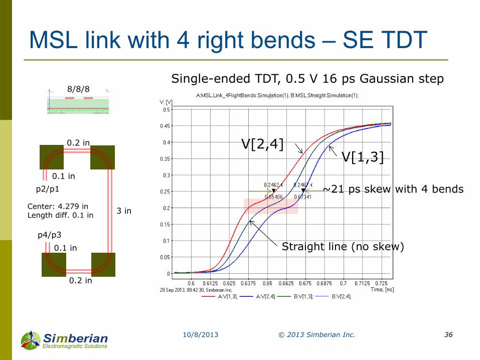
MSL link with 4 right bends – SE TDT
10/8/2013 © 2013 Simberian Inc. 36
0.2 in
0.2 in
3 in
0.1 in
0.1 in
Center: 4.279 in Length diff. 0.1 in
~21 ps skew with 4 bends
V[1,3] V[2,4]
Straight line (no skew)
8/8/8
p2/p1
p4/p3
Single-ended TDT, 0.5 V 16 ps Gaussian step

MSL link with 4 right bends – MM TDT
10/8/2013 © 2013 Simberian Inc. 37
0.2 in
0.2 in
3 in
0.1 in
0.1 in
Center: 4.279 in Length diff. 0.1 in
V[D1,D2]
8/8/8
D1/C1
D2/C2
Mixed-mode TDT, 0.5 V 16 ps Gaussian step
V[D1,C2] - FEMT
V[D1,C1] - NEMT
Straight – green line

MSL link with 4 right bends: “Skew” view on S-parameters
How to fix it? – match length?
10/8/2013 © 2013 Simberian Inc. 38
FEMT S[D1,C2]
NEMT S[D1,C1]
S[D1,D2]
S[D1,D1]
Straight
With 4 bends
With 4 bends
8/8/8

MSL link with 4 right bends and serpentine – SE TDT
10/8/2013 © 2013 Simberian Inc. 39
0.2 in
0.2 in
1.45 in 0.1 in
0.1 in
Center: 4.279 in Length diff. 0
8/8/8
p2/p1
p4/p3
Mixed-mode TDT, 0.5 V 16 ps Gaussian step
~7 ps max skew with 4 bends and serpentine
V[1,3]
V[2,4]
Straight line (no skew) 1.45 in
0.1 in

MSL link with 4 right bends and serpentine: “Skew” view on S-parameters
Length match did not fix the problem!
10/8/2013 © 2013 Simberian Inc. 40
FEMT S[D1,C2]
NEMT S[D1,C1]
S[D1,D2]
S[D1,D1]
Straight
With 4 bends and serpentine
With 4 bends and serpentine
8/8/8

MSL link with 4 right bends and serpentine: “Skew” view on S-parameters
Actually made it worse: MT at lower frequencies
10/8/2013 © 2013 Simberian Inc. 41
FEMT S[D1,C2]
NEMT S[D1,C1]
S[D1,D2]
S[D1,D1]
With 4 bends
With 4 bends and serpentine
With 4 bends
8/8/8
With 4 bends and serpentine

MSL link with 4 right bends and serpentine – MM TDT
10/8/2013 © 2013 Simberian Inc. 42
V[D1,D2]
8/8/8 Mixed-mode TDT, 0.5 V 16 ps Gaussian step
V[D1,C2] - FEMT
V[D1,C1] - NEMT
Straight – green line
0.2 in
0.2 in
1.45 in 0.1 in
0.1 in
Center: 4.279 in Length diff. 0
D1/C1
D2/C2 1.45 in
0.1 in
Length match in microstrip link clearly did not work! May be it was not done properly?

MSL link with 2 right and 2 left bends – SE TDT
10/8/2013 © 2013 Simberian Inc. 43
0.2 in
0.2 in
3 in
0.1 in
0.1 in
Center: 4.279 in Length diff. 0
2 right + 2 left bends (V[1,3] and V[2,4] overlap)
Straight line (no skew)
8/8/8
p2/p1
p4/p3
Single-ended TDT, 0.5 V 16 ps Gaussian step
The best we can do, but did it solver the problem?

MSL link with 2 right + 2 left bends: “Skew” view on S-parameters Still problem with insertion loss
and mode transformation!
10/8/2013 © 2013 Simberian Inc. 44
FEMT S[D1,C2]
NEMT S[D1,C1]
S[D1,D2]
S[D1,D1]
Straight
With 2 right + 2 left bends
With 2 right + 2 left bends
8/8/8

MSL link with 2 right + 2 left bends and serpentine – MM TDT
10/8/2013 © 2013 Simberian Inc. 45
V[D1,D2]
8/8/8 Mixed-mode TDT, 0.5 V 16 ps Gaussian step
V[D1,C2] - FEMT V[D1,C1] - NEMT
Straight – green line
Length match in microstrip link does not work? Let’s try to figure out why…
0.2 in
0.2 in
3 in
0.1 in
0.1 in
Center: 4.279 in Length diff. 0
D1/C1
D2/C2

MSL back-to-back right and left bends
10/8/2013 © 2013 Simberian Inc. 46
8/8/8 Only small close complimentary bends reduce the mode transformation and skew and EMI!
0.1 in
Length diff. 0
0.1 in
V[D1,C2] - FEMT FEMT S[D1,C2]
Rb=108 mil
Rb=28 mil
Rb=108 mil
Rb=28 mil
~10 dB

Why length matching does not work for microstrip lines? Energy along the coupled MSL propagate in even and odd modes and they
have different propagation velocity or group delay:
10/8/2013 © 2013 Simberian Inc. 47
Even mode (++)
Odd mode (+-)
Quasi-static solver Full-wave solver
Even mode (++)
Odd mode (+-)
Will length compensation work if no difference in mode velocity (strip lines)? … Depends on how you do it – see Simbeor FRSI examples on skew in diff strips…

Practical example of length matching
10/8/2013 © 2013 Simberian Inc. 48
Diff. Return Loss
Diff. TDR
Serpentines may be worse then vias!

Cross-talk in vias 8-layer stackup from CMP-28 benchmark board from
Wild River Technology, http://wildrivertech.com Dielectric and conductor models are identified with GMS-parameters
10/8/2013 © 2013 Simberian Inc. 49
p1
p2
p3
p4
NEXT – S[1,3]
FEXT – S[1,4]

Single-ended vias – case 1 Two coupled vias in a 150 x 150 mil area caged with PEC wall (stitching vias) Vias are 20 mil apart, antipad diameters 40 mil, 13 mil MSL; The first cage resonance is at about 10 GHz (half wavelength in dielectric)
10/8/2013 © 2013 Simberian Inc. 50
p1
p2
p3
p4
NEXT
FEXT

Single-ended vias – case 2
10/8/2013 © 2013 Simberian Inc. 51
Two un-coupled vias in a 150 x 150 mil area caged with PEC wall (stitching vias ) Vias are 60 mil apart, antipad diameters 40 mil Separation reduced NEXT below 25 GHz, but FEXT is increased above 10 GHz –
vias are coupled through the cavity (may be the whole board)!
p1
p2
p3
p4
FEXT
NEXT

Single-ended vias – case 3
10/8/2013 © 2013 Simberian Inc. 52
Two shielded vias in a 150 x 150 mil area caged with PEC wall (stitching vias) Vias are 60 mil apart, antipad diameters 40 mil, stitching vias are 20 mil from the signal
vias – localized up to about 30 GHz No cross-talk due to the localization – also models for such vias do not depend on the
caging or simulation area!
p1
p2
p3
p4
FEXT
NEXT

Cross-talk in single-ended vias
10/8/2013 © 2013 Simberian Inc. 53
NEXT FEXT
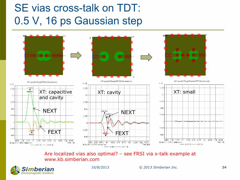
SE vias cross-talk on TDT: 0.5 V, 16 ps Gaussian step
10/8/2013 © 2013 Simberian Inc. 54
XT: capacitive and cavity
XT: cavity XT: small
FEXT
NEXT
FEXT
NEXT
Are localized vias also optimal? – see FRSI via x-talk example at www.kb.simberian.com

Cross-talk in differential vias
10/8/2013 © 2013 Simberian Inc. 55
p1
p2
p3
p4
NEXT – S[D1,D3]
FEXT – S[D1,D4]
Two coupled differential vias in a 120 x 120 mil area caged with PEC wall Vias are 30 mil apart, antipad 25x55 mil, traces 8 mil MSL, 8 mil separation; The first cage resonance is at about 12 GHz (half wavelength in dielectric) Stackup from CMP-28 board, Wild River Technology http://wildrivertech.com
Three cases:
20 mil 40 mil 40 mil + 5 vias

Cross-talk in differential vias
10/8/2013 © 2013 Simberian Inc. 56
NEXT FEXT

Differential vias cross-talk on TDT: 0.5 V, 16 ps Gaussian step
10/8/2013 © 2013 Simberian Inc. 57
XT: capacitive and cavity XT: cavity XT: small
FEXT
NEXT
FEXT
NEXT
Are localized vias also optimal? – see FRSI via x-talk example at www.kb.simberian.com

Benchmarking or validation How to make sure that the analysis works? – Validation boards! Consistent board manufacturing is the key for success
Fiber type, resin content, copper roughness must be strictly specified or fixed!!!
Include a set of structures to identify one material model at a time Solder mask, core and prepreg, resin and glass, roughness, plating,…
Include a set of structures to identify accuracy for transmission lines and typical discontinuities Use identified material models for all structures on the board consistently No tweaking - discrepancies should be investigated
Use VNA/TDNA measurements and compare both magnitude and phase (or group delay) of all S-parameters
10/8/2013 © 2013 Simberian Inc. 58

Example of benchmarking boards
10/8/2013 59
PLRD-1 (Teraspeed Consulting, DesignCon 2009, 2010)
CMP-08 (Wild River Technology & Teraspeed Consulting, DesignCon 2011)
CMP-28, Wild River Technology, DesignCon 2012 Isola, EMC 2011, DesignCon 2012
© 2013 Simberian Inc.

Conclusion
10/8/2013 © 2013 Simberian Inc. 60
Validate all ideas with EM analysis Build only things that can be reliably analyzed! Decompositional analysis is the fastest and most
accurate way to simulate interconnects ONLY IF All S-parameter models in the link are qualified Material parameters are properly identified Interconnects are designed as localized waveguides Manufacturer, measurements and models are benchmarked
Examples created for this presentation are available at www.kb.simberian.com (use FRSI keyword)

Contact and resources Yuriy Shlepnev, Simberian Inc.,
[email protected] Tel: 206-409-2368
Webinars on decompositional analysis, S-parameters quality and material identification http://www.simberian.com/Webinars.php
Simberian web site and contacts www.simberian.com Demo-videos http://www.simberian.com/ScreenCasts.php App notes http://www.simberian.com/AppNotes.php Technical papers http://kb.simberian.com/Publications.php Presentations http://kb.simberian.com/Presentations.php Download Simbeor® from www.simberian.com and try it on your
problems for 15 days
10/8/2013 © 2013 Simberian Inc. 61
Related Documents