LM53635-Q1 MSP430G2332 LP5912-Q1 Speaker Connections SN74LVC125A-Q1 PCM1865-Q1 PCM1865-Q1 LP5907-Q1 Analog Inputs Power EMI Filter TAS6424-Q1 TAS6424-Q1 +3.3 V I 2 C +5 V PVDD PVDD TDM TDM +5 V I 2 C LM74610-Q1 Copyright © 2017, Texas Instruments Incorporated 1 TIDUCZ2 – December 2017 Submit Documentation Feedback Copyright © 2017, Texas Instruments Incorporated Reference Design for Automotive 8-Ch Class-D Amplifier With 2.1-MHz Switching Power Supply TI Designs: TIDA-00733 Reference Design for Automotive 8-Ch Class-D Amplifier With 2.1-MHz Switching Power Supply Description This reference design shows how to implement an eight-channel, Class-D amplifier that is capable of driving 2-Ω loads and an off-battery step-down power supply with 5-V and 3.3-V outputs. The amplifier design provides audio inputs for each audio channel. A high-performance audio analog-to-digital converter (ADC) creates the digital data stream from the audio inputs and creates the digital timing for the system. Resources TIDA-00733 Design Folder TAS6424-Q1 Product Folder LM53635-Q1 Product Folder PCM1865-Q1 Product Folder LP5907-Q1 Product Folder LP5912-Q1 Product Folder LM74610-Q1 Product Folder ASK Our E2E Experts Features • Audio Output Power: 45 W per Channel at 10% THD + N • Wide Power Supply Voltage Range of 4.5 V to 18 V • 40-V Load Dump Protection • Passes CISPR 25 Class 5 Radiated Emissions Applications • Head Unit • Premium Amplifier An IMPORTANT NOTICE at the end of this TI reference design addresses authorized use, intellectual property matters and other important disclaimers and information.

Welcome message from author
This document is posted to help you gain knowledge. Please leave a comment to let me know what you think about it! Share it to your friends and learn new things together.
Transcript

LM53635-Q1
MSP430G2332
LP5912-Q1
Spe
aker
C
onne
ctio
ns
SN74LVC125A-Q1PCM1865-Q1
PCM1865-Q1
LP5907-Q1
Ana
log
Inpu
ts
Pow
er
EMI Filter
TAS6424-Q1
TAS6424-Q1
+3.3 V
I2C
+5 VPVDD
PVDD
TDM
TDM
+5 V
I2C
LM74610-Q1
Copyright © 2017, Texas Instruments Incorporated
1TIDUCZ2–December 2017Submit Documentation Feedback
Copyright © 2017, Texas Instruments Incorporated
Reference Design for Automotive 8-Ch Class-D Amplifier With 2.1-MHzSwitching Power Supply
TI Designs: TIDA-00733Reference Design for Automotive 8-Ch Class-D AmplifierWith 2.1-MHz Switching Power Supply
DescriptionThis reference design shows how to implement aneight-channel, Class-D amplifier that is capable ofdriving 2-Ω loads and an off-battery step-down powersupply with 5-V and 3.3-V outputs. The amplifierdesign provides audio inputs for each audio channel. Ahigh-performance audio analog-to-digital converter(ADC) creates the digital data stream from the audioinputs and creates the digital timing for the system.
Resources
TIDA-00733 Design FolderTAS6424-Q1 Product FolderLM53635-Q1 Product FolderPCM1865-Q1 Product FolderLP5907-Q1 Product FolderLP5912-Q1 Product FolderLM74610-Q1 Product Folder
ASK Our E2E Experts
Features• Audio Output Power: 45 W per Channel at
10% THD + N• Wide Power Supply Voltage Range of
4.5 V to 18 V• 40-V Load Dump Protection• Passes CISPR 25 Class 5 Radiated Emissions
Applications• Head Unit• Premium Amplifier
An IMPORTANT NOTICE at the end of this TI reference design addresses authorized use, intellectual property matters and otherimportant disclaimers and information.
System Description www.ti.com
2 TIDUCZ2–December 2017Submit Documentation Feedback
Copyright © 2017, Texas Instruments Incorporated
Reference Design for Automotive 8-Ch Class-D Amplifier With 2.1-MHzSwitching Power Supply
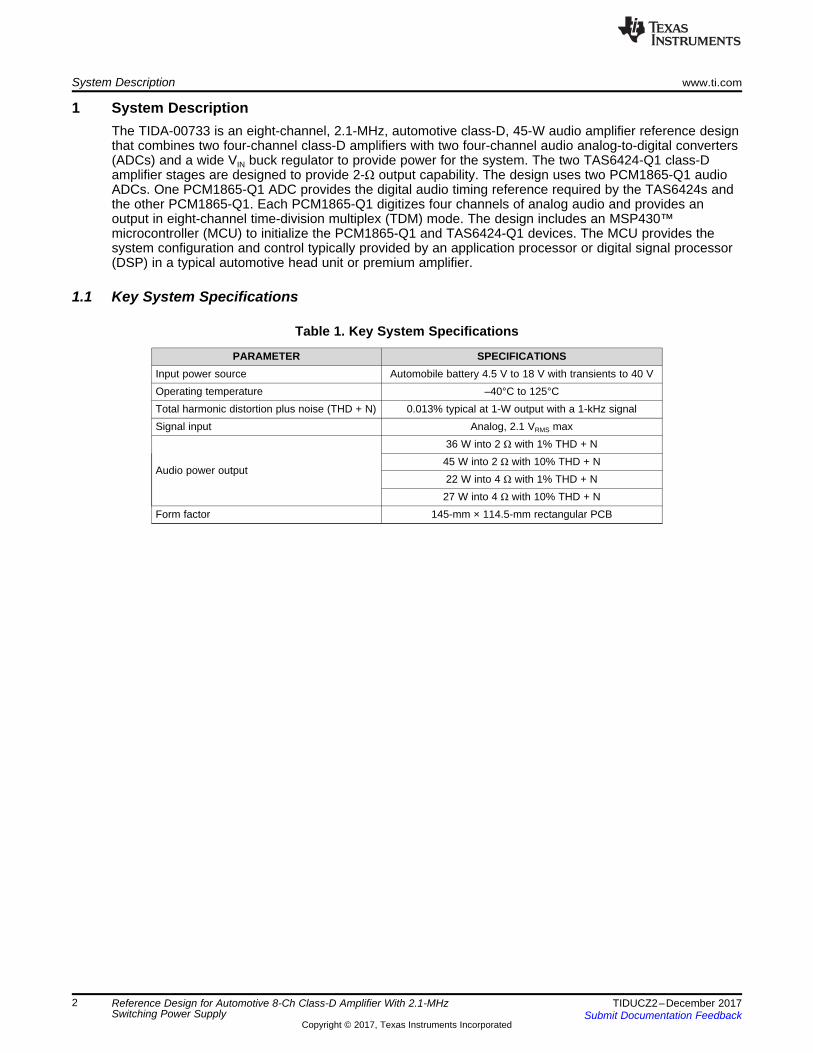
1 System DescriptionThe TIDA-00733 is an eight-channel, 2.1-MHz, automotive class-D, 45-W audio amplifier reference designthat combines two four-channel class-D amplifiers with two four-channel audio analog-to-digital converters(ADCs) and a wide VIN buck regulator to provide power for the system. The two TAS6424-Q1 class-Damplifier stages are designed to provide 2-Ω output capability. The design uses two PCM1865-Q1 audioADCs. One PCM1865-Q1 ADC provides the digital audio timing reference required by the TAS6424s andthe other PCM1865-Q1. Each PCM1865-Q1 digitizes four channels of analog audio and provides anoutput in eight-channel time-division multiplex (TDM) mode. The design includes an MSP430™microcontroller (MCU) to initialize the PCM1865-Q1 and TAS6424-Q1 devices. The MCU provides thesystem configuration and control typically provided by an application processor or digital signal processor(DSP) in a typical automotive head unit or premium amplifier.
1.1 Key System Specifications
Table 1. Key System Specifications
PARAMETER SPECIFICATIONSInput power source Automobile battery 4.5 V to 18 V with transients to 40 VOperating temperature –40°C to 125°CTotal harmonic distortion plus noise (THD + N) 0.013% typical at 1-W output with a 1-kHz signalSignal input Analog, 2.1 VRMS max
Audio power output
36 W into 2 Ω with 1% THD + N45 W into 2 Ω with 10% THD + N22 W into 4 Ω with 1% THD + N27 W into 4 Ω with 10% THD + N
Form factor 145-mm × 114.5-mm rectangular PCB

LM53635-Q1
MSP430G2332
LP5912-Q1
Spe
aker
C
onne
ctio
ns
SN74LVC125A-Q1PCM1865-Q1
PCM1865-Q1
LP5907-Q1
Ana
log
Inpu
ts
Pow
er
EMI Filter
TAS6424-Q1
TAS6424-Q1
+3.3 V
I2C
+5 VPVDD
PVDD
TDM
TDM
+5 V
I2C
LM74610-Q1
Copyright © 2017, Texas Instruments Incorporated
www.ti.com System Overview
3TIDUCZ2–December 2017Submit Documentation Feedback
Copyright © 2017, Texas Instruments Incorporated
Reference Design for Automotive 8-Ch Class-D Amplifier With 2.1-MHzSwitching Power Supply
2 System Overview
2.1 Block Diagram
Figure 1. TIDA-00733 Block Diagram
2.2 Design ConsiderationsThis design has several requirements beyond the primary specifications listed in the previous Table 1.
The design must have a 3.3-V power supply on the board to power the digital portions of the circuit. Theboard must also have a way to configure itself so that it does not require external software to test theboard.
VDD VCOM VBAT GVDD PVDD
OUT_1P
OUT_1M
OUT_2P
OUT_2M
OUT_3P
OUT_3M
OUT_4P
OUT_4M
VREG
I2C_ADDR1
I2C_ADDR0
SDA
SCL
I2C Control
SDIN1
SDIN2
SCLK
FSYNC
MCLK
Serial
Audio
Port
PLL and Clock
Management
STANDBY
WARN
FAULT
Digital Core
Reference
Regulators
Gate Drive
Regulator
Channel 1
Powerstage
Channel 2
Powerstage
Channel 3
Powerstage
Channel 4
Powerstage
Volume Control
-100 to +24 dB
0.5 dB steps
Gate
Drives
Digital to PWM
Clip
Detection
Closed Loop Class D Amplifier
Overcurrent Limit
Protection
Overcurrent
Overtemperature
Overvoltage and Undervoltage
DC Detection
Short to GND
DC Load Diagnostics
Short to Power
Open Load
Shorted Load
AC Load Diagnostics
MUTE
Copyright © 2016, Texas Instruments Incorporated
System Overview www.ti.com
4 TIDUCZ2–December 2017Submit Documentation Feedback
Copyright © 2017, Texas Instruments Incorporated
Reference Design for Automotive 8-Ch Class-D Amplifier With 2.1-MHzSwitching Power Supply
2.3 Highlighted Products
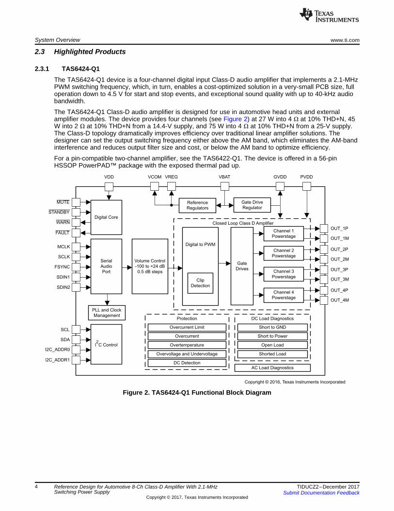
2.3.1 TAS6424-Q1The TAS6424-Q1 device is a four-channel digital input Class-D audio amplifier that implements a 2.1-MHzPWM switching frequency, which, in turn, enables a cost-optimized solution in a very-small PCB size, fulloperation down to 4.5 V for start and stop events, and exceptional sound quality with up to 40-kHz audiobandwidth.
The TAS6424-Q1 Class-D audio amplifier is designed for use in automotive head units and externalamplifier modules. The device provides four channels (see Figure 2) at 27 W into 4 Ω at 10% THD+N, 45W into 2 Ω at 10% THD+N from a 14.4-V supply, and 75 W into 4 Ω at 10% THD+N from a 25-V supply.The Class-D topology dramatically improves efficiency over traditional linear amplifier solutions. Thedesigner can set the output switching frequency either above the AM band, which eliminates the AM-bandinterference and reduces output filter size and cost, or below the AM band to optimize efficiency.
For a pin-compatible two-channel amplifier, see the TAS6422-Q1. The device is offered in a 56-pinHSSOP PowerPAD™ package with the exposed thermal pad up.
Figure 2. TAS6424-Q1 Functional Block Diagram

+-+
-
CONTROLLOGIC DRIVER
HS CURRENTSENSE
LS CURRENTSENSE
OSCILLATOR
PWMCOMP.
ERROR AMPLIFIER
MODELOGIC
RESETCONTROL
SW
VIN
PGND
FB
EN
FPWM
INT. REG.BIAS
BIASVCC
CBOOT
SYNC
AGND
*
*
* = Not used in -ADJ
RESET
1.0 VReference
�
ENABLELOGIC
Copyright © 2016, Texas Instruments Incorporated
www.ti.com System Overview
5TIDUCZ2–December 2017Submit Documentation Feedback
Copyright © 2017, Texas Instruments Incorporated
Reference Design for Automotive 8-Ch Class-D Amplifier With 2.1-MHzSwitching Power Supply
2.3.2 LM53635-Q1The LM53625-Q1/LM53635-Q1 synchronous buck regulator is optimized for automotive applications,providing an output voltage of 5 V, 3.3 V, or an adjustable output (see Figure 3). Advanced high-speedcircuitry allows the LM53625-Q1/LM53635-Q1 to regulate from an input of 18 V to an output of 3.3 V at afixed frequency of 2.1 MHz. Innovative architecture allows this device to regulate a 3.3-V output from aninput voltage of only 3.55 V. All aspects of the LM53625- Q1/LM53635-Q1 are optimized for automotiveand performance-driven industrial customers. An input voltage range up to 36 V, with transient toleranceup to 42 V, eases input surge protection design. The automotive-qualified HotRod™ QFN package withwettable flanks reduces parasitic inductance and resistance while increasing efficiency, minimizing switchnode ringing, and dramatically lowering electromagnetic interference (EMI). An open-drain reset output,with built-in filtering and delay, provides a true indication of system status. This feature negates therequirement for an additional supervisory component, which saves on cost and board space. Theseamless transition between pulse-width modulation (PWM) and pulse-frequency modulation (PFM)modes and low quiescent current (only 15 μA for the 3.3-V option) ensure high efficiency and superiortransient responses at all loads.
Figure 3. LM53635-Q1 Functional Block Diagram

Mix,
Mux
PrimaryADC
(CH2L)
Secondary
ADC
PrimaryADC
(CH1R)
VINL 4 (4M)
VINL3 (4P)
VINL2 (1M)
VINL1 (1P)
Mix,
Mux
VINR1 (2P)
VINR2 (2M)
VINR4 (3M)
VINR3 (3P)
MD0/Mode
MD1/ADR1/MS
MD2/SDA/MOSI
MD3/SCL/SBCK
MD4/MISO/GPIO0
MD5/(INT A/ DMIM/GPIO1)
MD6/(DM CLK/GPIO2)
INT/(INT C/GPIO3)
Control ,
GPIO,
Interrupt and
Digital Mic
Interface
DOUT
Clocks, PLLPower
LD
O
DG
ND
DV
DD
IOV
DD
AG
ND
AV
DD XI
XO
SC
K
BC
K
LR
CK
PCM1865-Q1
ReferenceVREF
Mic Bias
AudioSerial
Port
(LJ, I2S,
TDM)
PrimaryADC
(CH1L)
PrimaryADC
(CH2R)
DOUT 2
DM
IC/
DIN
Co
ntr
ol,
GP
IO,In
terr
up
t,
Dig
italM
icIn
terf
ace
Mix
erand
Ener
gys
ens
e
DS
Ps
Copyright © 2017, Texas Instruments Incorporated
System Overview www.ti.com
6 TIDUCZ2–December 2017Submit Documentation Feedback
Copyright © 2017, Texas Instruments Incorporated
Reference Design for Automotive 8-Ch Class-D Amplifier With 2.1-MHzSwitching Power Supply
2.3.3 PCM1865-Q1The PCM1865-Q1 audio front-end device takes a new approach to audio-function integration to easecompliance with European Ecodesign legislation while enabling high-performance end products (seeFigure 4). Smaller, smarter products are becoming increasingly feasible at reduced costs without therequirement for a 5-V supply or an external programmable-gain amplifier.
The highly-flexible audio front end of the PCM1865-Q1 supports input levels from small-mV microphoneinputs to 2.1-VRMS line inputs without external resistor dividers. The PCM1865-Q1 integrates many system-level functions that assist or replace some digital signal processing (DPS) functions.
All of these features are available using a single 3.3-V power supply. An integrated band-gap voltagereference provides excellent power supply rejection ratio (PSRR) such that a dedicated analog 3.3-V railmay not be required.
Figure 4. PCM1865-Q1 Simplified Block Diagram

IN
VBG1.20V
EN
+ ENEN
GND
POR
+
OUT
1 M VIH
RFCF
+
EN
EN
RAD
Copyright © 2016, Texas Instruments Incorporated
www.ti.com System Overview
7TIDUCZ2–December 2017Submit Documentation Feedback
Copyright © 2017, Texas Instruments Incorporated
Reference Design for Automotive 8-Ch Class-D Amplifier With 2.1-MHzSwitching Power Supply
2.3.4 LP5907-Q1The LP5907-Q1 is a low-noise low-dropout linear regulator (LDO) that can supply 250 mA of outputcurrent (see Figure 5). Designed to meet the requirements of RF and analog circuits, the LP5907-Q1device provides low noise, high PSRR, low quiescent current, and low line- or load-transient responsefigures. Using new innovative design techniques, the LP5907-Q1 offers class-leading noise performancewithout a noise bypass capacitor and the ability for remote output capacitor placement.
The device is designed to work with a 1-μF input and a 1-μF output ceramic capacitor (and does notrequire a separate noise bypass capacitor).
This device is available with fixed output voltages from 1.2 V to 4.5 V in 25-mV steps. Contact TexasInstruments Sales for specific voltage option requirements.
Figure 5. LP5907-Q1 Functional Block Diagram

Current LimitIN OUT
EN Control
EN
Output Discharge
140-µsDELAY
PG
GND
3 M �
RAD100 �
Copyright © 2016, Texas Instruments Incorporated
EA
VIN
+±
VBG
45 k �
System Overview www.ti.com
8 TIDUCZ2–December 2017Submit Documentation Feedback
Copyright © 2017, Texas Instruments Incorporated
Reference Design for Automotive 8-Ch Class-D Amplifier With 2.1-MHzSwitching Power Supply
2.3.5 LP5912-Q1The LP5912-Q1 is a low-noise LDO that can supply up to 500 mA of output current (see Figure 6).Designed to meet the requirements of RF and analog circuits, the LP5912-Q1 device provides low noise,high PSRR, low quiescent current, and low line- and load-transient response. The LP5912-Q1 offersclass-leading noise performance without a noise bypass capacitor and with the ability for remote outputcapacitance placement.
The device is designed to work with a 1-μF input and a 1-μF output ceramic capacitor (and does notrequire a separate noise bypass capacitor).
This device is available with fixed output voltages from 0.8 V to 5.5 V in 25-mV steps. Contact TexasInstruments Sales for specific voltage option requirements.
Figure 6. LP5912-Q1 Functional Block Diagram

DS
G
LOGIC
Reverse Batt Shut OffCharge
PumpVCAPH
VCAPL
CATHODEGATE PULL DOWNGATE DRIVEANODE
Input Output
11.5 V
www.ti.com System Overview
9TIDUCZ2–December 2017Submit Documentation Feedback
Copyright © 2017, Texas Instruments Incorporated
Reference Design for Automotive 8-Ch Class-D Amplifier With 2.1-MHzSwitching Power Supply
2.3.6 LM74610-Q1The LM74610-Q1 is a controller device which is specified for use with an N-Channel MOSFET in areverse polarity protection circuitry (see Figure 7). The device is designed to drive an external MOSFET toemulate an ideal diode rectifier when connected in series with a power source. A unique advantage of thisscheme is that it is not referenced to ground and thus has zero IQ.
The LM74610-Q1 controller provides a gate drive for an external N-Channel MOSFET and a fast-responseinternal comparator to discharge the MOSFET gate in the event of reverse polarity. This fast pulldownfeature limits the amount and duration of reverse current flow if opposite polarity is sensed. The devicedesign also meets CISPR25 Class-5 EMI specifications and automotive ISO7637 transient requirementswith a suitable transient voltage suppression (TVS) diode.
Figure 7. LM74610-Q1 Functional Block Diagram

1
2 3
4
5 6
8
10
9
11
13
12
3OE
3A
4OE
4A
1OE
1A
2OE
2A
1Y
2Y
3Y
4Y
System Overview www.ti.com
10 TIDUCZ2–December 2017Submit Documentation Feedback
Copyright © 2017, Texas Instruments Incorporated
Reference Design for Automotive 8-Ch Class-D Amplifier With 2.1-MHzSwitching Power Supply
2.3.7 SN74LVC125A-Q1The SN74LVC125A-Q1 quadruple-bus buffer gate is designed for 1.65-V to 3.6-V VCC operation (seeFigure 8).
The SN74LVC125A-Q1 features independent line drivers with three-state outputs. Each output is disabledwhen the associated output-enable (OE) input is high.
To ensure the high-impedance state during power up or power down, OE must be tied to VCC through apullup resistor; the current-sinking capability of the driver determines the minimum value of the resistor.
Drive the inputs from either 3.3-V or 5-V devices, for which they are specified. This feature allows the useof this device as a translator in a mixed 3.3-V or 5-V system environment.
Figure 8. SN74LVC125A-Q1 Logic Diagram (Positive Logic)
2.3.8 TLV2462A-Q1The devices in the TLV246x-Q1 family of low-power rail-to-rail input and output operational amplifiers arewell suited for battery management systems in electric vehicles (EVs), hybrid electric vehicles (HEVs), andpowertrain as well as lighting and roof module systems in body and lighting applications. The inputcommon-mode voltage range extends beyond the supply rails for maximum dynamic range in low-voltagesystems. The amplifier output has rail-to-rail performance with high-output-drive capability, solving one ofthe limitations of older rail-to-rail input and output operational amplifiers. This rail-to-rail dynamic range andhigh output drive make the TLV246x-Q1 ideal for buffering ADCs.
The operational amplifier has a 6.4-MHz bandwidth and a 1.6-V/µs slew rate with only 500-µA supplycurrent, which provides good AC performance with low-power consumption. Devices are available with anoptional shutdown terminal, which places the amplifier in an ultra-low supply current mode (IDD = 0.3 µAper channel). While in shutdown, the operational amplifier output enters a high-impedance state. DCapplications are also well served with an input noise voltage of 11 nV/√Hz and input offset voltage of100 µV.
Figure 9 shows the TLV2462A-Q1 functional block diagram.
Figure 9. TLV2462A-Q1 Functional Block Diagram

Clock
System
Brownout
Protection
RST/NMI
DVCC DVSS
MCLK
Watchdog
WDT+
15-Bit
Timer0_A3
3 CC
Registers
16MHz
CPU
incl. 16
Registers
Emulation
2BP
JTAG
Interface
SMCLK
ACLK
MDB
MAB
Port P1
8 I/O
Interrupt
capability
pullup/down
resistors
P1.x
8
Spy-Bi
Wire
XIN XOUT
RAM
256B
256B
256B
128B
Flash
8KB
4KB
2KB
1KB
P2.x
Port P2
up to 8 I/O
Interrupt
capability
pullup/down
resistors
up to 8
USI
Universal
Serial
Interface
SPI, I2C
ADC
10-Bit
8 Ch.
Autoscan
1 ch DMA
www.ti.com System Overview
11TIDUCZ2–December 2017Submit Documentation Feedback
Copyright © 2017, Texas Instruments Incorporated
Reference Design for Automotive 8-Ch Class-D Amplifier With 2.1-MHzSwitching Power Supply
2.3.9 MSP430G2332The Texas Instruments MSP430™ family of ultra-low-power MCUs consist of several devices featuringdifferent sets of peripherals targeted for various applications. The architecture, combined with five low-power modes is optimized to achieve extended battery life in portable measurement applications. Thedevice features a powerful 16-bit RISC CPU, 16-bit registers, and constant generators that contribute tomaximum code efficiency. The digitally controlled oscillator (DCO) allows wake-up from low-power modesto active mode in less than 1 μs.
The MSP430G2332 series of MCUs are ultra-low-power, mixed-signal microcontrollers with built-in 16-bittimers and up to 16 I/O touch-sense enabled pins and built-in communication capability using theuniversal serial communication interface (see Figure 10). The MSP430G2332 series have a 10-bit ADC.For configuration details, see the Available Options table in the MSP430G2xx2 data sheet. Typicalapplications include low-cost sensor systems that capture analog signals, convert them to digital values,and then process the data for display or for transmission to a host system.
Figure 10. MSP430G2332 Functional Block Diagram

System Overview www.ti.com
12 TIDUCZ2–December 2017Submit Documentation Feedback
Copyright © 2017, Texas Instruments Incorporated
Reference Design for Automotive 8-Ch Class-D Amplifier With 2.1-MHzSwitching Power Supply
2.4 System Design Theory
2.4.1 Hardware OverviewThis user's guide instructs how to evaluate several different functions of components used in the design.The PCM1865-Q1 is shown as both the timing master and slave in this configuration and the twoPCM1865-Q1 digital outputs are tied together to provide eight-channel digital audio. The TDM timing anddata signals are buffered using an SN74LVC125A-Q1 quad buffer. The TDM input provides timing for theTAS6424-Q1 amplifiers. The TAS6424-Q1 provides audio outputs capable of driving 2-Ω- or 4-Ω speakerloads. The LM53635-Q1 buck regulator supplies 5 V, which is used to power the LP5907-Q1 and LP5912-Q1 regulators and also provides enough capacity to power other in-system loads. The LP5907-Q1 andLP5912-Q1 devices each provide 3.3 V to different parts of the circuit. The LM74610-Q1 circuit replaces arectifier diode to reduce the power loss while still providing reverse voltage protection.
The TIDA-00733 is designed to use an enclosure to simulate the housing used in a typical head unit orpremium amplifier. The enclosure, a Hammond 1590J, provides EMI shielding in addition to acting as thesystem heat sink after installing the TIDA-00733 design within.
Figure 11 and Figure 12 show the complete TIDA-00733 PCB.
Figure 11. TIDA-00733 PCB—Top Figure 12. TIDA-00733 PCB—Bottom
2.4.1.1 PCB Outline and InterfaceThe printed-circuit board (PCB) for the TIDA-00733 is designed to create the shortest path for power tothe TAS6424-Q1 class-D amplifiers. The board size is 145 mm × 114.5 mm (5.7 in × 4.5 in). Some of theboard area is required for the necessary connectors to bring in external audio signals, the powerconnectors, and the speaker output connectors. The primary circuitry fits in an area that is 86.9 mm ×114.5 mm (3.4 in × 4.5 in).

www.ti.com System Overview
13TIDUCZ2–December 2017Submit Documentation Feedback
Copyright © 2017, Texas Instruments Incorporated
Reference Design for Automotive 8-Ch Class-D Amplifier With 2.1-MHzSwitching Power Supply
2.4.1.2 PowerThe TIDA-00733 is designed to be powered by an automotive 12-V power system. The TAS6424-Q1device has two power rails which connect directly to a main power input. The VBAT is connected to theTAS6424-Q1 at pin 3. VBAT can be in the range of 4.5 V to 18 V. PVDD must be in the range of 4.5 V to 26.4V. The VBAT limits the input voltage range of the TIDA-00733 design due to its lower maximum level. Therest of the components in the system operate at 3.3 V; therefore regulators are provided to create 3.3 Vfrom the 5 V that the LM53635L circuit supplies.
The main power input from the battery is filtered with a pi filter to reduce noise entering the system as wellas reducing noise conducted out of the system on the power lines. Capacitors C81, C82, C147, C150, andC151 are on the input side and are placed in different places along the power input line to provide filteringwhere necessary. C81, C147, C150, and C151 along with R86 provide a filter just inside the systemenclosure to short any high-frequency noise on the power lines and prevent the noise from entering orexiting the system. C82 is placed between these capacitors and the main filter inductor, L18. C140 is thelast section of the pi filter and the LM74610 smart diode circuit. The pi filter further reduces any noise onthe power line. The construction of L18 is very important. L18 must be a shielded inductor to reduce EMIemissions. A non-shielded inductor can act as an antenna and receive emissions inside the box andcouple them onto the power line. This EMI can then be radiated outside the box.
2.4.1.2.1 LM74610-Q1The LM74610-Q1 provides reverse battery protection when using it in conjunction with an N-channelMOSFET (see Figure 13). The MOSFET is connected with the source and drain pins reversed from thenormal connection. This configuration allows the body diode to conduct if the MOSFET is off and the inputpower is connected. A charge pump in the LM74610 charges capacitor C152 and uses the stored voltageto provide the gate drive to MOSFET Q1. The benefit to this circuit is that the amount of power dissipatedin the reverse protection circuit is much lower than it would be than when using a typical Schottky rectifierbecause the voltage drop is much lower with the MOSFET. This observation is very important in designslike the TIDA-00733 where load currents as high as 40 A are possible.

0.1µF
50V
C81
VBAT
GND
1000 µF50V
C1
1000 µF50V
C41
GND
PVDD
Bulk Filter Caps
0.1µF
50V
C147
4.7µF
50V
C82
4.7µF
50V
C140
IHLP5050CEERR47M01
470nH
Vishay-Dale
L18T1
CB35-36-CY
T2
CB35-36-CY
0.1µF
50V
C83
D6
SMBJ14A-13-F
17V
D5
SMBJ17A-13-F
0.1µF
50V
C150
0.1µF
50V
C151
0.51
R86
VCAPL1
GATE PULL DOWN2
NC3
ANODE4
NC5
GATE DRIVE6
VCAPH7
CATHODE8
LM74610QDGKRQ1
U11
GATE5
CATHODE4
VCAP1
EN3
GND2
ANODE6
LM74700QDDCRQ1
U12
DNP
2.2µF
C152
2.2µF
C153DNP
GND
PVDD
4
7,81,2,3
5,6,
Q1
BSC014N04LSI
VIN_FLT
Copyright © 2017, Texas Instruments Incorporated
System Overview www.ti.com
14 TIDUCZ2–December 2017Submit Documentation Feedback
Copyright © 2017, Texas Instruments Incorporated
Reference Design for Automotive 8-Ch Class-D Amplifier With 2.1-MHzSwitching Power Supply
Figure 13. LM74610-Q1 Smart Diode Circuit and Power Input

www.ti.com System Overview
15TIDUCZ2–December 2017Submit Documentation Feedback
Copyright © 2017, Texas Instruments Incorporated
Reference Design for Automotive 8-Ch Class-D Amplifier With 2.1-MHzSwitching Power Supply
2.4.1.2.2 LM53635L-Q1The LM53635L-Q1 regulator provides a regulated 5-VDC for use by the linear regulators and as a source ofpower for auxiliary loads (see Figure 14). The LM53635L-Q1 has been selected because of its inputvoltage range (4 V to 36 V), efficiency, and electromagnetic interference (EMI) performance. TheLM53635L-Q1 is a fixed 5-V output device. The LM53635L-Q1 also has spread-spectrum operation whenused without synchronization. Spread-spectrum operation improves EMI performance.
The LM53635L-Q1 circuit follows the recommendations from the data sheet for choosing components.The power input is filtered with two 10-uF capacitors and two 0.1-uF capacitors placed on each side of thepart to provide balanced filter paths at the LM53635-Q1 (U3) input.
R24 pulls the U1 pin 16 to the input voltage PVDD. Pin 16, which is called FPWM, controls the operatingmode of the LM53635L-Q1 device. Pulling pin 16 low sets U1 for auto light-load mode, which is notemployed in this system. Pin 16 is pulled high to force PWM mode all of the time; this configuration limitsthe efficiency of the LM53635L-Q1 at light loads by forcing the switching frequency to remain the same.This outcome is desirable in an audio system to reduce the possible creation of audible beat frequenciesthat couple into the audio path due to skipped pulses, which effectively lower the switching frequency. Pin16 must also be pulled high if using an external synchronization signal with the LM53635L-Q1.
At the output of the LM53635L-Q1 circuit, C84 provides the boost required to drive the N-channelMOSFET switch of the LM53635-Q1 device. R9 is provided to slow any transients (if present). C98 andR13 are a snubber for high-frequency transients. L9, C91, C92, and C93 provide the necessary outputfiltering for the regulated +5 V. L9 is a shielded inductor to reduce EMI effects. Pin 22 provides an internalbias to the LM53635L-Q1 device and is connected to the output through R22 and C146, which provide alow-pass filter. C146 is tied to pin 20, AGND, before they have both been connected to the main systemground through a net-tie. VCC is also bypassed to AGND through C94. LED D7 is connected to the 5-Voutput as a power-on indicator. J10 is provided to connect an external load to test the power outputcapability. D7 and J10 are placed outside the area where the box encloses the main part of the circuit.

PS_SYNC
22µF
16V
C91
22µF
16V
C92
22µF
16V
C9310µF
50V
C89
0.1µF
50V
C90
0.1µF
50V
C87
10µF
50V
C88DNP10µF
50V
C86
GND
GND
GND
0.47 µF
25V
C84
GND
PVDD
0
R260
R24
0
R28DNP
5_BIAS
SW_5
FPWM
DNI
FPWM - High = Force PWM, Low = Auto Light Load. Must be high for sync
nRESET_PS
TP5
Green
21
D7
GND
10µF
50V
C85DNP 3.0
R22
909
R25
VCC1
CBOOT2
SYNC3
PVIN14
PGND15
PGND16
PGND17
PGND18
SW9
PGND210
PGND211
PGND212
PGND213
PVIN214
AVIN15
FPWM16
NC17
EN18
RESET19
AGND20
FB21
BIAS22
U3
LM53635LQRNLRQ1
GND
1
2
J10
1714955
+5V
0.1µF
50V
C146
AGND
5_BIAS
XAL6030-222MEB
2.2µH
L9
4.7µF
10V
C94
100k
R20DNP
GND
1000pF
50V
C98
3.0
R9
8.06
R13
GND
10.0
R18FB5
5_BOOT
AGND
AGND
AGND GND
NTG
Net-Tie
Copyright © 2017, Texas Instruments Incorporated
System Overview www.ti.com
16 TIDUCZ2–December 2017Submit Documentation Feedback
Copyright © 2017, Texas Instruments Incorporated
Reference Design for Automotive 8-Ch Class-D Amplifier With 2.1-MHzSwitching Power Supply
Figure 14. LM53635L-Q1 Regulator Circuit

+3P3V_A
Total ON BOARD 3.3 V Analog Current = 90 mA
VIN1
GND2
EN3
N/C4
VOUT5
U5
LP5907MFX-3.3/NOPB
GND
GND
1µF25V
C1421µF25V
C143
0
R19
GND
GND
1µF25V
C1451µF25V
C144
+5V+3P3V
Total ON BOARD 3.3 V Current = 232 mA
OUT1
NC2
PG3
EN4
GND5
IN6
PAD7
U6
LP5912Q3.3DRVRQ1
GND
0R21
DNP
Copyright © 2017, Texas Instruments Incorporated
www.ti.com System Overview
17TIDUCZ2–December 2017Submit Documentation Feedback
Copyright © 2017, Texas Instruments Incorporated
Reference Design for Automotive 8-Ch Class-D Amplifier With 2.1-MHzSwitching Power Supply
2.4.1.2.3 LP5907-Q1 and LP5912-Q1Two linear regulators are provided for +3.3 V. U6, the LP5912-Q1, is used for all digital +3.3-Vrequirements, which includes the MSP430, the digital part of the PCM8165-Q1 devices, theSN74LVC125A-Q1 logic buffer, and the VDD connections on the TAS6424-Q1 devices. U5, the LP5907-Q1, provides +3.3 V for the analog portions of the PCM1865-Q1 devices to ensure low noise in the ADCsof the two parts. R21 is provided to allow testing with U5 removed.
Figure 15 shows the LP5912-Q1 and LP5907-Q1 circuits.
Figure 15. LP5912-Q1 and LP5907-Q1 Circuits
System Overview www.ti.com
18 TIDUCZ2–December 2017Submit Documentation Feedback
Copyright © 2017, Texas Instruments Incorporated
Reference Design for Automotive 8-Ch Class-D Amplifier With 2.1-MHzSwitching Power Supply
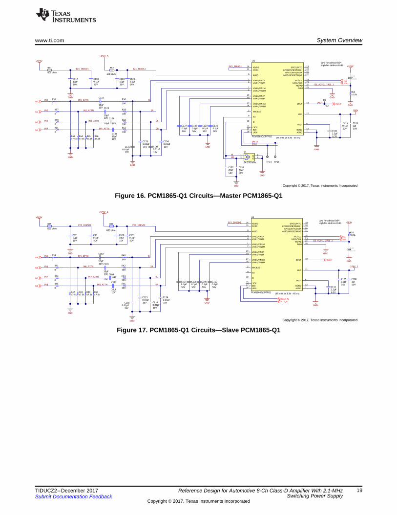
2.4.1.3 PCM1865-Q1The PCM1865-Q1 is ideal for this design (see Figure 16 and Figure 17). Eight ADC channels are requiredto provide the eight channels of digital data for the two TAS6424-Q1 devices.
The PCM1865-Q1 has an internal clock generator to create the TDM data stream. U9 is configured as atiming master and provides timing for U1, U2, and U8. A 24.576-MHz crystal, Y1, is the oscillator timingreference.
The power to the PCM1865-Q1 is +3.3 V. The digital I/O and internal digital circuits are supplied throughthe IOVDD and DVDD pins 14 and 13, which are connected together. The PCM1865-Q1 generates high-frequency digital signals and noise that can couple onto pins 13 and 14. This high-frequency noise cancouple to the board power lines and become radiated emissions. R35 and R51, at U8 and U9 respectively,are ferrites that provide high-frequency filtering to reduce the probability of high-frequency emissions.Power supply filtering and bypass capacitors C97, C99, C117, and C118 are placed close to pins 13 and14 of the two PCM1865-Q1 devices. The +3.3 V for the analog section, AVDD, is filtered by C100, C101,C120, and C121.All of the 0.1-µF capacitors are placed close to the power pins on the PCM1865-Q1devices to provide transient filtering. Two ferrites, R36 and R52, provide high-frequency filtering of the+3.3-V power to prevent noise from affecting the sensitive ADC portions of the ICs.
The four analog inputs of each PCM1865-Q1 are configured as single-ended inputs. Several passivecomponents are required to couple the analog signal into each ADC channel of the PCM1865-Q1 device.Each input has a 47.5-kΩ impedance which is set by a resistor to ground. A 0-Ω series resistor is providedto create a resistive divider with the 47.5-kΩ resistor if the input voltage will exceed 2.1 VRMS. Next, a 10-µF capacitor AC couples the input. This circuit is followed by a 100-Ω resistor and a 0.01-µF capacitor toprovide a low-pass filter with a cutoff frequency of 159 kHz. The high cutoff frequency is chosen to ensurethat the signal has only been attenuated by –0.077 dB at 20 kHz and that the signal bandwidth is sufficientfor the 96-kHz sampling frequency of the PCM1865s. All eight analog inputs have the same circuit. Thedesigner can also use several unpopulated resistors to connect the different inputs together so that onesignal source can drive multiple channels. The eight input channels have a corresponding output channelon a TAS6424-Q1 device.
The digital interface on the PCM1865-Q1 devices include an I2C interface and the digital audio interface.The I2C interface connects to the system MCU and is used to configure the PCM1865-Q1 devices. Thedigital audio interface consists of three signals: SCLK, LRCLK, and DOUT. SCLK is the serial or BIT clock.In some applications and on the PCM1865-Q1 data sheet, this signal is called BCLK or BCK. The LRCLKsignal is the left-right clock, also known as the word clock. This clock indicates the start of a data frame forTDM configured data. The frequency of LRCLK is equal to the sampling clock frequency. DOUT is thedata output. The TDM output is configured for eight data words to be compatible with the TDMrequirements of the TAS6424-Q1. The DOUT data words are 24 bits each, though the data stream isconfigured for 32-bit words. For this design, the audio sampling rate is 96 kHz. Consequently, SCLK is24.576 MHz. The designer can set the audio sampling rate to either 48 kHz or 44.1 kHz if desired. U9 isconfigured as the timing master and provides the two timing signals as well as filling the first four data timeslots for TDM. PCM1865-Q1 U8 receives timing and provides data outputs in the last four TDA time slots.The DOUT pins of the two PCM1865-Q1 devices are tied together. When a PCM1865-Q1 output is idle, itis in a high-impedance state so that the other PCM1865-Q1 device can drive the output. In this way, twoPCM1865-Q1 devices provide a single data stream for TDM.
Low for adress 0x94High for address 0x96
SCLK_P2
LRCLK_P2
DOUT
0.1µF
50V
C99
+3P3V
10µF
10V
C97
GND
600 ohm
R35 3V3_1865A2
+3P3V_A
3V3_1865D2
GND
GND
SCL
SDA
47.5kR50
47.5kR49
47.5kR48
47.5kR47
GND
3L
4L
3R
IN5
IN7
IN6
IN8
0
R39
0
R41
0
R45
IN5_ATTN
IN6_ATTN
IN8_ATTN
I2S_ADSEL_1865_2
GND
+3P3V
145 mW at 3.3V - 45 ma
GND
1P8V_2
0.01µF16V
C115
0.01µF
16V
C113
0.01µF
16V
C1160.01µF
16V
C114
100
R40
100
R44
100
R42
100
R46
GND
4R
600 ohm
R36
0
R43
VINL1/VIN1P3
VINR1/VIN2P4
VINL2/VIN1M1
VINR2/VIN2M2
VINL3/VIN4P29
VINR3/VIN3P30
VINL4/VIN4M27
VINR4/VIN3M28
AVDD8
DVDD13
IOVDD14
AGND7
DGND12
LDO11
VREF6
MICBIAS5
XO9
XI10
SCKI15
BCK17
LRCK16
DOUT18
MD026
MS/AD25
MC/SCL24
MOSI/SDA23
MISO/GPIO0/DMIN222
GPIO2/INTB/DMCLK20
GPIO1/INTA/DMIN21
GPIO3/INTC19
U8
PCM1865QDBTRQ1
IN7_ATTN
IN5
IN6
IN7
IN8
10.0kR37
10.0kR38
DNP
0.1µF
50V
C10110µF
10V
C100
10µF
10V
C102
10µF
10V
C103
10µF10V
C104
10µF
10V
C1120.1µF
50V
C1070.1µF
50V
C1080.1µF
50V
C1090.1µF
50V
C110 0.1µF
50V
C1051µF
50V
C106
2.2µF
6.3V
C111
3V3_1865D2
Copyright © 2017, Texas Instruments Incorporated
1µF
50V
C126
DOUT
+3P3V
0.1µF
50V
C12110µF
10V
C117
GND
600 ohm
R51 3V3_1865A1
10µF
10V
C120
+3P3V_A
3V3_1865D1
0.1µF
50V
C125
2.2µF
6.3V
C131
GND
10µF10V
C122
10µF 10V
C124
10µF10V
C123
10µF10V
C132
GND
SCL
SDA
47.5kR66
47.5kR65
47.5kR64
47.5kR63
GND
1L
2L
1R
IN1
IN3
IN2
IN4
0
R55
0
R57
0
R61
IN1_ATTN
IN2_ATTN
I2S_ADSEL_1865_1
10.0kR53
DNP
GND
+3P3V
1
3 4
2GG
24.576 MHz
Y1
20pF
50V
C13720pF
50V
C138
GND
GND
145 mW at 3.3V - 45 ma
Low for adress 0x94High for address 0x96
0.1µF
50V
C1270.1µF
50V
C1280.1µF
50V
C1290.1µF
50V
C130
GND
1P8V
XIXO
TP14 TP15
0.01µF16V
C135
0.01µF
16V
C133
0.01µF
16V
C1360.01µF
16V
C134
100
R56
100
R60
100
R58
100
R62
GND
2R
0.1µF
50V
C118
600 ohm
R52
10.0kR54
0
R59
SCLKLRCLK
VINL1/VIN1P3
VINR1/VIN2P4
VINL2/VIN1M1
VINR2/VIN2M2
VINL3/VIN4P29
VINR3/VIN3P30
VINL4/VIN4M27
VINR4/VIN3M28
AVDD8
DVDD13
IOVDD14
AGND7
DGND12
LDO11
VREF6
MICBIAS5
XO9
XI10
SCKI15
BCK17
LRCK16
DOUT18
MD026
MS/AD25
MC/SCL24
MOSI/SDA23
MISO/GPIO0/DMIN222
GPIO2/INTB/DMCLK20
GPIO1/INTA/DMIN21
GPIO3/INTC19
U9
PCM1865QDBTRQ1
IN3_ATTN
IN1
IN2
IN3
IN4
DOUT
TP12
IN4_ATTN
3V3_1865D1
Copyright © 2017, Texas Instruments Incorporated
www.ti.com System Overview
19TIDUCZ2–December 2017Submit Documentation Feedback
Copyright © 2017, Texas Instruments Incorporated
Reference Design for Automotive 8-Ch Class-D Amplifier With 2.1-MHzSwitching Power Supply
Figure 16. PCM1865-Q1 Circuits—Master PCM1865-Q1
Figure 17. PCM1865-Q1 Circuits—Slave PCM1865-Q1

VCC14
1A2
GND7
1OE1
1Y3
2A5
4Y11
2OE4
4OE13
2Y6
4A12
3A9
3Y8
3OE10
U10
SN74LVC125AQPWRQ1
0.1µF50V
C139
+3P3V
GND
GND
SCLK
54.9
R67
54.9
R68
54.9
R69
LRCLK
54.9
R70
54.9
R71
54.9
R72
SCLK_T1
SCLK_T2
SCLK_P2
LRCLK_T1
LRCLK_T2
LRCLK_P2
SCLK_B1
LRCLK_B
54.9
R81
54.9
R80
DOUT DOUT_B
DOUT_T1
DOUT_T2
Copyright © 2017, Texas Instruments Incorporated
System Overview www.ti.com
20 TIDUCZ2–December 2017Submit Documentation Feedback
Copyright © 2017, Texas Instruments Incorporated
Reference Design for Automotive 8-Ch Class-D Amplifier With 2.1-MHzSwitching Power Supply
2.4.1.4 SN74LVC125A-Q1An SN74LVC125A-Q1 quad buffer is provided to add drive strength to the TDM signals (see Figure 18).SCLK and LRCLK both have three loads, while DOUT has two. PCM1865-Q1 U9 drives the clock signalsSCLK and LRCLK to the SN74LVC125A-Q1 device and the buffered clock outputs are routed toPCM1865-Q1 U8 and the two TAS6424-Q1 devices through separate PCB traces. The signals areseparated with one resistor for each path to isolate the signals and to provide a way to reduce signalovershoot and undershoot at the load ends. The two PCM1865-Q1 DOUT signals are connected togetherand fed through the SN74LVC125A-Q1 and the two TAS6424-Q1 devices, again through separateresistors and traces. The output series resistors are paced near the SN74LVC125A-Q1 to provide the bestsignal correction. The value for the resistors was chosen to reduce signal undershoot on the signals whilestill providing adequate rise and fall time for the TAS6424-Q1 devices and the slave PCM1865-Q1. Theseresistors help to reduce EMI by reducing the strength of undesired high-frequency signals.
Figure 18. SN74LVC125A-Q1 Circuit

www.ti.com System Overview
21TIDUCZ2–December 2017Submit Documentation Feedback
Copyright © 2017, Texas Instruments Incorporated
Reference Design for Automotive 8-Ch Class-D Amplifier With 2.1-MHzSwitching Power Supply
2.4.1.5 TAS6424-Q1The TAS6424-Q1 is a 75-W class-D audio power amplifier that operates with a switching frequency of 2.1MHz (see Figure 19 and Figure 20). The TAS6424-Q1 has a digital audio input which is compatible withI2S and TDM digital audio data. The digital audio input enables a system designer to eliminate an analogsignal chain that connects from an audio digital-to-analog converter (DAC), through the circuit board, andto the power amplifier. Removing this analog signal chain reduces the risk of noise interference in theaudio signal. The TAS6424-Q1 has load dump protection, so the designer can connect the power pins forPVDD and PVDD directly to the car battery system. The TIDA-00733 design uses two TAS6424-Q1 devices,U1 and U2.
The TAS6424-Q1 has three voltage inputs. VDD is a logic-level supply connected at U1 pin 19 and must bein the range of 3 V to 3.5 V. VBAT is connected to the TAS6424-Q1 at pin 3. PVDD connects to U1 pins 2,29, 30, 42, 43, 55, and 56. Other voltages are generated inside the TAS6424-Q1. VREG is an internalregulator, which is bypassed to AREF through a capacitor. VCOM is an internal reference, which is alsobypassed to AREF. The two voltages GVDD form the gate drive for the output high-side MOSFETs. Pin 9 isthe GVDD for outputs 3 and 4 while pin 10 is the GVDD for outputs 1 and 2. Both pins are bypassed toground with 1-µF capacitors.
Pins 12 through 16 form the digital audio input to the TAS6424-Q1 device from the PCM1865-Q1 device.Pin 20, MCLK, is tied directly to SCLK because MCLK and SCLK can be the same frequency when usinga TDM input. Pins 20 and 21 are the I2C interface. Pins 22 and 23 set the address for the I2C. In thisdesign, U1 and U2 require different addresses so that the designer may configure them differently. Pin 24is the nSTANDBY function. If the designer sets this signal low, the TAS6424-Q1 device is in a low-powerstandby state. This function is not for use in TIDA-00733. Pin 25 is the nMUTE function. When this signalis low, the outputs of the TAS6424-Q1 are muted, but the operating state of the device is maintained. Pins24 and 25 must be pulled up by resistors or a processor for the TAS6424-Q1 device to operate. Pins 26and 27, /FAULT and /WARN, are open-drain outputs. These pins function as light-emitting diode (LED)drivers, as Figure 20 shows, or as processor interrupts. Pin 26 is asserted low when a defined faultcondition exists. Pin 27 is asserted low when clipping occurs or if the TAS6424-Q1 device has passed theovertemperature warning threshold. For further details, see TAS6424-Q1 75-W, 2-MHz Digital Input 4-Channel Automotive Class-D Audio Amplifier With Load-Dump Protection and I2C Diagnostics .
Each output channel is a bridge-tied load (BTL) output. This topology requires a low-pass filter for both thepositive- and negative-going outputs of each channel. The output inductors for TIDA-00733 have beenchosen to provide enough current capacity to power 2-Ω loads. A dual inductor has been used to savespace. The two inductors in each package are not magnetically coupled together.

AVDD8
BST_1M31
BST_1P35
BST_2M37
BST_2P41
BST_3M44
BST_3P48
BST_4M50
BST_4P54
FSYNC14
GND33
GND7
GND36
GND39
GND11
GND1
GND46
GND18
GND49
GND28
GND52
AREF4
GVDD10
GVDD9
I2C_ADDR022
I2C_ADDR123
MCLK12
OUT_1M32
OUT_1P34
OUT_2M38
OUT_2P40
OUT_3M45
OUT_3P47
OUT_4M51
OUT_4P53
PVDD30
PVDD2
PVDD42
PVDD43
PVDD29
PVDD55
PVDD56
GND17
SCL20
SCLK13
SDA21
SDIN115
SDIN216
VBAT3
VCOM6
VDD19
VREG5
FAULT26
MUTE25
STANDBY24
WARN27
U1
TAS6424QDKQRQ1
1µF
50V
C17
1µF
50V
C25
1µF
50V
C31
1µF
50V
C39
0.01 µF
50V
C11
2.2µF
C14
GND
GND
GND
GND
GND
GND
GND
GND
GND
GND
OUT1M
OUT1P
OUT2M
OUT2P
OUT3M
OUT3P
OUT4M
OUT4P
OUT5+
OUT7-
OUT7+
OUT6+
OUT6-
OUT8+
OUT8-
OUT5-
0.1µF
50V
C3
2.2µF
C16
2.2µF
C19
2.2µF
C22
2.2µF
C27
2.2µF
C28
2.2µF
C33
2.2µF
C34
1µF
50V
C35
1µF
50V
C37
1µF
50V
C12
1µF
50V
C10
0.01 µF
50V
C13
0.01 µF
50V
C18
0.01 µF
50V
C26
0.01 µF
50V
C32
0.01 µF
50V
C36
0.01 µF
50V
C38
0.01 µF
50V
C40
PVDD
1µF
25V
C20
GND
PVDD
0
R1 U1_VBAT
4.99k
R3
10.0kR5
1µF
25V
C23
1µF
25V
C24
1µF25V
C291µF25V
C30
1µF25V
C21AREF
GND
AVDD_GND
AVDD_GND10.0kR6
+3P3V
nSTANDBY
nMUTE
100k
R7DNP
100k
R4DNP
4.99k
R8
GND
+3P3V
I2C_A0
I2C_A1
SCL
SDA
SCLK_T1
LRCLK_T1
DOUT_T1
+3P3V
1µF25V
C15
GND
GND
0.1µF
50V
C510µF
50V
C4
PVDD
GND
0.1µF
50V
C710µF
50V
C6
PVDD
GND
0.1µF
50V
C910µF
50V
C8
PVDD
I2C Address
Bit State I2C Address(A1/A0)
00 0xD4/0xD501 0xD6/0xD710 0xD8/0xD911 0xDA/0xDB
nSTANDBY
nMUTE
OUT8+OUT8-OUT7+OUT7-OUT6+OUT6-OUT5+OUT5-
150060YS75000Yellow
2 1
D2
150060SS75000Super Red
2 1
D1
1.00k
R10
1.00k
R11DNP
+3P3V
nFAULT
10µF
50V
C2
3.3µH
1 234
L1VAMV06077E-3R3MM2
3.3µH
1 234
L2VAMV06077E-3R3MM2
3.3µH
1 234
L3VAMV06077E-3R3MM2
3.3µH
1 234
L4VAMV06077E-3R3MM2
nWARN
5
4
1
2
3
6
7
8
J1
OSTTE080161
GND
Caution Caution Hot surface.
Contact may cause burns.
Do not touch
Copyright © 2017, Texas Instruments Incorporated
System Overview www.ti.com
22 TIDUCZ2–December 2017Submit Documentation Feedback
Copyright © 2017, Texas Instruments Incorporated
Reference Design for Automotive 8-Ch Class-D Amplifier With 2.1-MHzSwitching Power Supply
Figure 19. TAS6424-Q1 Class-D Power Audio Amplifier Circuits (Part 1 of 2)

AVDD8
BST_1M31
BST_1P35
BST_2M37
BST_2P41
BST_3M44
BST_3P48
BST_4M50
BST_4P54
FSYNC14
GND33
GND7
GND36
GND39
GND11
GND1
GND46
GND18
GND49
GND28
GND52
AREF4
GVDD10
GVDD9
I2C_ADDR022
I2C_ADDR123
MCLK12
OUT_1M32
OUT_1P34
OUT_2M38
OUT_2P40
OUT_3M45
OUT_3P47
OUT_4M51
OUT_4P53
PVDD30
PVDD2
PVDD42
PVDD43
PVDD29
PVDD55
PVDD56
GND17
SCL20
SCLK13
SDA21
SDIN115
SDIN216
VBAT3
VCOM6
VDD19
VREG5
FAULT26
MUTE25
STANDBY24
WARN27
U2
TAS6424QDKQRQ1
1µF
50V
C71
1µF
50V
C79
2.2µF
C54
GND
GND
GND
GND
GND
GND
OUTSM
OUTSP
OUTCM
OUTCP
OUT3M2
OUT3P2
OUT4M2
OUT4P2
0.1µF
50V
C45
2.2µF
C56
2.2µF
C59
2.2µF
C62
2.2µF
C67
2.2µF
C68
2.2µF
C73
2.2µF
C74
1µF
50V
C75
1µF
50V
C77
0.01 µF
50V
C72
0.01 µF
50V
C76
0.01 µF
50V
C78
0.01 µF
50V
C80
10µF
50V
C44
PVDD
0.1µF
50V
C60
GND
PVDD
U2_VBAT
100k
R14DNP
1µF25V
C63
1µF25V
C691µF25V
C70
1µF25V
C61AREF2
GND
AVDD2_GND
nSTANDBY
nMUTE
100k
R16DNP
4.99k
R15
4.99k
R17
GND
+3P3V
I2CB_A0
I2CB_A1
SCL
SDA
SCLK_T2
LRCLK_T2
DOUT_T2
+3P3V
1µF25V
C55
GND
GND
0.1µF
50V
C4710µF
50V
C46
PVDD
GND
0.1µF
50V
C4910µF
50V
C48
PVDD
GND
0.1µF
50V
C5110µF
50V
C50
PVDD
I2C Address
Bit State I2C Address(A1/A0)
00 0xD4/0xD501 0xD6/0xD710 0xD8/0xD911 0xDA/0xDB
nSTANDBY
nMUTE
1µF
50V
C42
GND
GND
OUT4+
1µF
50V
C52
0.01 µF
50V
C43
0.01 µF
50V
C53
OUT4-
1µF
50V
C57
GND
GND
OUT3+
1µF
50V
C64
0.01 µF
50V
C58
0.01 µF
50V
C65
OUT3-
OUT1-OUT1+OUT2-OUT2+OUT3-OUT3+OUT4-OUT4+
nFAULT
0
R12
AVDD2_GND
OUT1-
OUT1+
OUT2-
OUT2+
1µF
25V
C66
3.3µH
1 234
L6
VAMV06077E-3R3MM2
3.3µH
1 234
L5VAMV06077E-3R3MM2
3.3µH
1 234
L7VAMV06077E-3R3MM2
3.3µH
1 234
L8VAMV06077E-3R3MM2
nWARN
5
4
1
2
3
6
7
8
J2
OSTTE080161
GND
Caution Caution Hot surface.
Contact may cause burns.
Do not touch
Copyright © 2017, Texas Instruments Incorporated
www.ti.com System Overview
23TIDUCZ2–December 2017Submit Documentation Feedback
Copyright © 2017, Texas Instruments Incorporated
Reference Design for Automotive 8-Ch Class-D Amplifier With 2.1-MHzSwitching Power Supply
Figure 20. TAS6424-Q1 Class-D Power Audio Amplifier Circuits (Part 2 of 2)

1
2
3
48
U4A
TLV2462AQDRQ1
5
6
7
48
U4B
TLV2462AQDRQ1
GND
GND
0.01µF50V
C148
0.01µF50V
C149
1.00k
R83
1.00k
R85
1.00k
R84
11.3k
R27
11.3k
R32
71.5k
R2
825
R23
221
R82
0.022µF
C141
GND
GND
GND
GND
1
2
J3
0022284023
1 2
J4 0022284023
SH-J1
SH-J2
+5V
1µF25V
C119
IN3
Copyright © 2017, Texas Instruments Incorporated
System Overview www.ti.com
24 TIDUCZ2–December 2017Submit Documentation Feedback
Copyright © 2017, Texas Instruments Incorporated
Reference Design for Automotive 8-Ch Class-D Amplifier With 2.1-MHzSwitching Power Supply
2.4.1.6 Support Circuits
2.4.1.6.1 TLV2462A-Q1 Oscillator CircuitTo run EMI tests, the ideal setup is to have a signal source on the board with the rest of the circuits. ATLV2462-Q1 dual operational amplifier (op amp) is used to provide this function (see Figure 21). One opamp, U4A, is configured as a 1-kHz square-wave oscillator. U4B provides a low-pass filter with a cutofffrequency of approximately 1.4 kHz so that the output approximates a sine wave. J3 connects the op ampto +5-V power, while J4 connects the output to the inputs of the PCM1865-Q1 devices. R23 and R25 areselected to drive the TAS6424-Q1 outputs to 1 W when a 2-Ω load has been connected.
Figure 21. TLV2462-Q1 Oscillator Circuit

DVCC1
P2.210
P2.311
P2.412
P2.513
P1.6/TA0.1/SDO/SCL/A6/TDI/TCLK14
P1.0/TA0CLK/ACLK/A02
P1.1/TA0.0/A13
P1.2/TA0.1/A24
P1.3/ADC10CLK/VREF-/VEREF-/A35
P1.4/TA0.2/SMCLK/A4/VREF+/VEREF+/TCK6
P1.5/TA0.0/SCLK/A5/TMS7
P2.08
P2.19
P1.7/SDI/SDA/A7/TDO/TDI15
RST/NMI/SBWTDIO16
TEST/SBWTCK17
XOUT/P2.718
XIN/TA0.1/P2.619
DVSS20
U7
MSP430G2332QPW2REP
+3P3V
SCL
SDA
0.1µF50V
C95
1
2
3
4
5
6
J5
851-43-006-20-001000
GND
0
0
R31DNP
nRST_TDIOSBWTCK
GND
GND
nRESET_PS10.0k
R34DNP
SCLSDA
nWARN
nFAULT
+3P3V
47.5kR33
+3P3V
GND
GND
DNP
DNP
21
S2
21
S3
VOL_DN
21
S1
VOL_UP
TP9TP8
2200pF
50V
C96
PS_SYNC
VOL_UPVOL_DN
Copyright © 2017, Texas Instruments Incorporated
www.ti.com System Overview
25TIDUCZ2–December 2017Submit Documentation Feedback
Copyright © 2017, Texas Instruments Incorporated
Reference Design for Automotive 8-Ch Class-D Amplifier With 2.1-MHzSwitching Power Supply
2.4.1.6.2 MSP430G2332-EPCreating a stand-alone design requires a host processor to configure the PCM1865-Q1 and TAS6424-Q1devices at power up. The MSP430G2332-EP has been chosen because this board design is intended foran extended temperature range. The I2C interface that connects to the PCM1865-Q1 and the TAS6424-Q1 devices is the primary interface from the MSP430 to the other components on the board (seeFigure 22). J5 is the programming interface for the MSP430. R33 and C96 provide a delayed power-upreset function. Switch S1 allows the user to reset the MSP430 without cycling power to the board. Thesignals nWARN1 and nFAULT1 are routed from theTAS6424-Q1 to the MSP430, but there is no provisionin the software to act upon faults or warnings. Switches S2 and S3 are provided for volume up and volumedown functions, though this has not been implemented. Pin 6 is an I/O that is routed to the LM53635L-Q1to provide an optional 2-MHz synchronization signal. The synchronization function is not implemented inthis reference design.
Figure 22. TIDA-00733 Microcontroller
2.4.2 SoftwareThe MSP430 used in the TIDA-00733 circuit board is required to configure the PCM1865-Q1 and TAS-6424-Q1 devices at power up. The program to accomplish this configuration is listed in the followingconfiguration code. The configuration program for TIDA-00733 is developed using the Code ComposerStudio™ (CCS) integrated development environment (IDE). Some of the software directives in theprogram are specific to CCS. The software is based on the software in TIDA-00743 and is very similar inoperation.

System Overview www.ti.com
26 TIDUCZ2–December 2017Submit Documentation Feedback
Copyright © 2017, Texas Instruments Incorporated
Reference Design for Automotive 8-Ch Class-D Amplifier With 2.1-MHzSwitching Power Supply
TIDA-00733 configuration code:#include <msp430.h>#include "USI_I2C.h"
//#define number_of_bytes 5 // How many bytes? MSK: This needs to go
//void Master_Transmit(void);//void Master_Transmit(char i2cAddress, unsigned char registerAddress, unsigned char writeValue);//void Master_Recieve(void);
//void Setup_USI_Master_TX(void); //will need to pass parameter to tell what themaster clock is so that the I2C clock sets up correctly//void Setup_USI_Master_RX(void); // - in both cases
unsigned char SLV_Test_Addr = 0x48;unsigned char PCM1_Addr = 0x4a; //PCM1865 Address - // 0x4Aunsigned char PCM2_Addr = 0x4b; //PCM1865 Address - // 0x4Bunsigned char TAS1_Addr = 0x6a; //TAS6424 Address // 0x6Aunsigned char TAS2_Addr = 0x6b; //TAS6424 Address // 0x6Bunsigned char Test_Reg = 0x10;unsigned char Test_Data = 0x2d;unsigned char Low_Vol = 0x0f;unsigned char EM_Vol = 0xd1;unsigned char Ful_Vol = 0xd5;unsigned char Volume = 0x0f;
//int I2C_State, Bytecount, Transmit = 0; // State variable//void Data_TX (void);//void Data_RX (void);int main(void){
volatile unsigned int i; // Use volatile to prevent removal
WDTCTL = WDTPW + WDTHOLD; // Stop watchdogif (CALBC1_1MHZ==0xFF) // If calibration constant erased{
while(1); // do not load, trap CPU!!}DCOCTL = 0; // Select lowest DCOx and MODx settingsBCSCTL1 = CALBC1_1MHZ; // Set DCODCOCTL = CALDCO_1MHZ;
P1OUT = 0xC0; // P1.6 & P1.7 Pullups, others to 0P1REN |= 0xC0; // P1.6 & P1.7 PullupsP1DIR = 0xFF; // Unused pins as outputsP2OUT = 0x00; //Make Sure FS = P2.2 is LOW so that CDCS503
multiplies by 1P2DIR = 0xFE;
__delay_cycles(10000);
Set_I2C();
__delay_cycles(10000);
//PCM1865 Master SectionI2C_Write (I2C_BYTE, PCM1_Addr, 0x20, 0x91); // Set as timing master on PCM1865I2C_Write (I2C_BYTE, PCM1_Addr, 0x26, 0x00); //Set BCLK Divider from SCK to 1 on PCM1865 -
96 kHz for LR CLKI2C_Write (I2C_BYTE, PCM1_Addr, 0x27, 0xff); //Sets BCK to LRCLK ratio to 256I2C_Write (I2C_BYTE, PCM1_Addr, 0x0b, 0x03);//set for TDM mode with 32 bit data slotsI2C_Write (I2C_BYTE, PCM1_Addr, 0x0c, 0x01);//Set for 4 channel TDMI2C_Write (I2C_BYTE, PCM1_Addr, 0x0d, 0x01);//Data offset from LRCLK rising edge. Set to 0x81
for the second four words 0x01 for the first four

www.ti.com System Overview
27TIDUCZ2–December 2017Submit Documentation Feedback
Copyright © 2017, Texas Instruments Incorporated
Reference Design for Automotive 8-Ch Class-D Amplifier With 2.1-MHzSwitching Power Supply
/* PCM1865 Slave Section - See if this changes input issue* should not need to set up master clock derivation* If needed, must set both register 0x20 and 0x28 bit 1
*/
I2C_Write (I2C_BYTE, PCM2_Addr, 0x0b, 0x03);//set for TDM mode with 32 bit data slotsI2C_Write (I2C_BYTE, PCM2_Addr, 0x0c, 0x01);//Set for 4 channel TDMI2C_Write (I2C_BYTE, PCM2_Addr, 0x0d, 0x81);//Data offset from LRCLK rising edge. Set to
0x81 for the second 4 words
//TAS6424 sectionI2C_Write (I2C_BYTE, TAS1_Addr, 0x00, 0x80); //Master Reset TAS6424 1.I2C_Write (I2C_BYTE, TAS2_Addr, 0x00, 0x80); //Master Reset TAS6424 2.
I2C_Write (I2C_BYTE, TAS1_Addr, 0x04, 0x55); // Mute outputs on TAS6424 1I2C_Write (I2C_BYTE, TAS2_Addr, 0x04, 0x55); // Mute outputs on TAS6424 2I2C_Write (I2C_BYTE, TAS1_Addr, 0x00, 0x80); //Master Reset TAS6424 1.I2C_Write (I2C_BYTE, TAS2_Addr, 0x00, 0x80); //Master Reset TAS6424 2.I2C_Write (I2C_BYTE, TAS1_Addr, 0x21, 0x80); //Clear Clock Fault TAS6424 1I2C_Write (I2C_BYTE, TAS2_Addr, 0x21, 0x80); //Clear Clock Fault TAS6424 2
I2C_Write (I2C_BYTE, TAS1_Addr, 0x01, 0x31); // Set Gain to Level 2 (15V) on TAS6424 1I2C_Write (I2C_BYTE, TAS2_Addr, 0x01, 0x31); // Set Gain to Level 2 (15V) on TAS6424 2
I2C_Write (I2C_BYTE, TAS1_Addr, 0x02, 0x62); // Set PWM for 44x FS on TAS6424 1I2C_Write (I2C_BYTE, TAS2_Addr, 0x02, 0x62); // Set PWM for 44x FS on TAS6424 2
I2C_Write (I2C_BYTE, TAS1_Addr, 0x03, 0x86); // Set Sampling Rate to 96 kHz, 1st 4 TDM slots onTAS6424 1
I2C_Write (I2C_BYTE, TAS2_Addr, 0x03, 0xA6); // Set Sampling Rate to 96 kHz, last 4 TDM slotson TAS6424 2
__delay_cycles(1000000);I2C_Write (I2C_BYTE, TAS1_Addr, 0x05, Low_Vol); // Turn down Channel 1 on TAS6424 1I2C_Write (I2C_BYTE, TAS1_Addr, 0x06, Low_Vol); // Turn down Channel 2 on TAS6424 1I2C_Write (I2C_BYTE, TAS1_Addr, 0x07, Low_Vol); // Turn down Channel 3 on TAS6424 1I2C_Write (I2C_BYTE, TAS1_Addr, 0x08, Low_Vol); // Turn down Channel 4 on TAS6424 1I2C_Write (I2C_BYTE, TAS2_Addr, 0x05, Low_Vol); // Turn down Channel 1 on TAS6424 2I2C_Write (I2C_BYTE, TAS2_Addr, 0x06, Low_Vol); // Turn down Channel 2 on TAS6424 2I2C_Write (I2C_BYTE, TAS2_Addr, 0x07, Low_Vol); // Turn down Channel 3 on TAS6424 2I2C_Write (I2C_BYTE, TAS2_Addr, 0x08, Low_Vol); // Turn down Channel 4 on TAS6424 2
Volume = EM_Vol;
I2C_Write (I2C_BYTE, TAS1_Addr, 0x04, 0x00); // Un-mute outputs on TAS6424 1I2C_Write (I2C_BYTE, TAS2_Addr, 0x04, 0x00); // Un-mute outputs on TAS6424 2
I2C_Write (I2C_BYTE, TAS1_Addr, 0x05, Volume); // Turn up Channel 1 on TAS6424 1I2C_Write (I2C_BYTE, TAS1_Addr, 0x06, Volume); // Turn up Channel 2 on TAS6424 1I2C_Write (I2C_BYTE, TAS1_Addr, 0x07, Volume); // Turn up Channel 3 on TAS6424 1I2C_Write (I2C_BYTE, TAS1_Addr, 0x08, Volume); // Turn up Channel 4 on TAS6424 1I2C_Write (I2C_BYTE, TAS2_Addr, 0x05, Volume); // Turn up Channel 1 on TAS6424 2I2C_Write (I2C_BYTE, TAS2_Addr, 0x06, Volume); // Turn up Channel 2 on TAS6424 2I2C_Write (I2C_BYTE, TAS2_Addr, 0x07, Volume); // Turn up Channel 3 on TAS6424 2I2C_Write (I2C_BYTE, TAS2_Addr, 0x08, Volume); // Turn up Channel 4 on TAS6424 2
// }
LPM0;}

System Overview www.ti.com
28 TIDUCZ2–December 2017Submit Documentation Feedback
Copyright © 2017, Texas Instruments Incorporated
Reference Design for Automotive 8-Ch Class-D Amplifier With 2.1-MHzSwitching Power Supply
The include file, msp430.h, is part of the MSP430Ware™ software library provided by Texas Instrumentsas an add-on to CCS. The include file USI_I2C.h defines the I2C commands used by the universal serialinterface (USI) block in the MSP430G2332. Next, variables are declared to represent the I2C addresses ofthe TAS6424-Q1 and the PCM1865-Q1 and various gain settings used in the program.
The main function starts after the declarations. The first commands are a test to ensure that the calibrationfor the MSP430 internal clock is valid. If the clock calibration is valid, the clock and the GPIO for banks 1and 2 are set up. This step is followed by a delay to ensure that the GPIO outputs are settled. The I2Csection is then set up.
The next section contains commands to configure the PCM1865-Q1 devices. The first command sets U9(PCM1) as the timing master:I2C_Write (I2C_BYTE, PCM1_Addr, 0x20, 0x91);
The next command sets the master clock-to-BCLK divide ratio. The command shown sets the BCLK to thesame value as the 24.576-MHz timing crystal. Note that BCLK, or bit clock, is the signal SCLK in theprevious schematic images.I2C_Write (I2C_BYTE, PCM1_Addr, 0x26, 0x00);
Following this, the BCLK to LRCLK ratio is set to 256:I2C_Write (I2C_BYTE, PCM1_Addr, 0x27, 0xff);
After the clocks have been set up, TDM mode is configured:I2C_Write (I2C_BYTE, PCM1_Addr, 0x0b, 0x03);I2C_Write (I2C_BYTE, PCM1_Addr, 0x0c, 0x01);I2C_Write (I2C_BYTE, PCM1_Addr, 0x0d, 0x01);
The write to address 0x0b sets the PCM1865-Q1 up for TDM mode with 32-bit time slots. The write toregister 0x0c sets the part for four-channel TDM and the write to 0x0d sets the data for a one-bit offsetfrom the rising edge of the LRCLK. This concludes the setup of the master PCM1865-Q1. The rest of theregisters are allowed to keep their default settings.
Next, the slave PCM1865-Q1 is configured:I2C_Write (I2C_BYTE, PCM2_Addr, 0x0b, 0x03);I2C_Write (I2C_BYTE, PCM2_Addr, 0x0c, 0x01);I2C_Write (I2C_BYTE, PCM2_Addr, 0x0d, 0x81)
These commands are the same as the TDM configuration commands for the master PCM1865-Q1 exceptthat the data is set for a 129-bit delay from LRCLK. This includes one bit offset in the first four channelsand 128 bits (four 32-bit words) of data delay until the master PCM1865-Q1 is done sending data. Thedata from U8 is then delivered in the data slots 5 through 8. The rest of the registers are allowed to keeptheir default settings. At this point, the audio data timing is present and analog signals at the inputs arebeing converted to digital data.
The TAS6424-Q1 configuration setting is more complicated:I2C_Write (I2C_BYTE, TAS1_Addr, 0x00, 0x80);I2C_Write (I2C_BYTE, TAS2_Addr, 0x00, 0x80);
I2C_Write (I2C_BYTE, TAS1_Addr, 0x04, 0x55);I2C_Write (I2C_BYTE, TAS2_Addr, 0x04, 0x55);
I2C_Write (I2C_BYTE, TAS1_Addr, 0x21, 0x80);I2C_Write (I2C_BYTE, TAS2_Addr, 0x21, 0x80);
I2C_Write (I2C_BYTE, TAS1_Addr, 0x01, 0x31);I2C_Write (I2C_BYTE, TAS2_Addr, 0x01, 0x31);

www.ti.com System Overview
29TIDUCZ2–December 2017Submit Documentation Feedback
Copyright © 2017, Texas Instruments Incorporated
Reference Design for Automotive 8-Ch Class-D Amplifier With 2.1-MHzSwitching Power Supply
All of the commands for the TAS6424-Q1 devices are first sent to TAS1 (U2) then to TAS2 (U1). The firsttwo commands in the TAS6424-Q1 configuration is a master reset for the TAS6424-Q1 devices. Thiscommand restarts the part. This command ensures the parts are in their default power-up state. The nextcommands ensure the outputs are muted so that nothing can be heard during configuration. The third pairof commands clears the clock fault register. At power up, a clock fault is registered because there is noclock input to the device until the PCM1865-Q1 master device has been configured. After the PCM1865-Q1 device has been configured, the TAS6424-Q1 operates correctly, but the fault register must be clearedby the host processor. The last two commands set the gain to be appropriate for a 15-V PVDD power rail.This setting ensures that the output reaches its maximum at 15 V. This setting is appropriate for the 14.4-V test level that is used to test the TIDA-00733 design. Register 0x01 also controls other functions: high-pass filter enable, global overtemperature warning control set point, overcurrent level set point, andvolume rate. These other functions are maintained at their default values.
The next commands configure the clocking for the TAS6424-Q1:I2C_Write (I2C_BYTE, TAS1_Addr, 0x02, 0x62);I2C_Write (I2C_BYTE, TAS2_Addr, 0x02, 0x62);
The first clock configuration command sets the PWM frequency to 44 times fs, where frame sync fs is thefrequency of the LRCLK. The Output Switch Frequency Option table in TAS6424-Q1 75-W, 2-MHz DigitalInput 4-Channel Automotive Class-D Audio Amplifier With Load-Dump Protection and I2C Diagnosticsshows that the PWM settings for either a 48-kHz sample rate or a 96-kHz sample rate results in a PWMfrequency of 2.11 MHz when bits 6 through 4 of register 0x02 are set to 110, or 6h. The other functions inregister 0x02 are set for their defaults.I2C_Write (I2C_BYTE, TAS1_Addr, 0x03, 0x86);I2C_Write (I2C_BYTE, TAS2_Addr, 0x03, 0xA6);__delay_cycles(100000);
The second clock configuration command sets the TAS6424-Q1 sampling rate to 96 kHz. This commandalso sets each TAs6424-Q1 for the TDM time slot from which to retrieve data. TAS1 retrieves data fromthe first four TDM time slots and TAS2 retrieves data from the second four TDM time slots.
At this point, the TAS6424-Q1 devices are operating correctly and user must turn up the volume. The gainsetting has no effect because the outputs are muted. Before setting the TAS6424-Q1 for a normal outputvolume, set the four channel gains for a very low value. Each channel has its own register for setting gain,so four register writes are made to each TAS6426 to set all channels for the same gain:I2C_Write (I2C_BYTE, TAS1_Addr, 0x05, Low_Vol);I2C_Write (I2C_BYTE, TAS1_Addr, 0x06, Low_Vol);I2C_Write (I2C_BYTE, TAS1_Addr, 0x07, Low_Vol);I2C_Write (I2C_BYTE, TAS1_Addr, 0x08, Low_Vol);I2C_Write (I2C_BYTE, TAS2_Addr, 0x05, Low_Vol);I2C_Write (I2C_BYTE, TAS2_Addr, 0x06, Low_Vol);I2C_Write (I2C_BYTE, TAS2_Addr, 0x07, Low_Vol);I2C_Write (I2C_BYTE, TAS2_Addr, 0x08, Low_Vol);
Volume = EM_Vol;
I2C_Write (I2C_BYTE, TAS1_Addr, 0x04, 0x00);I2C_Write (I2C_BYTE, TAS2_Addr, 0x04, 0x00);
I2C_Write (I2C_BYTE, TAS1_Addr, 0x05, Volume);I2C_Write (I2C_BYTE, TAS1_Addr, 0x06, Volume);I2C_Write (I2C_BYTE, TAS1_Addr, 0x07, Volume);I2C_Write (I2C_BYTE, TAS1_Addr, 0x08, Volume);I2C_Write (I2C_BYTE, TAS2_Addr, 0x05, Volume);I2C_Write (I2C_BYTE, TAS2_Addr, 0x06, Volume);I2C_Write (I2C_BYTE, TAS2_Addr, 0x07, Volume);I2C_Write (I2C_BYTE, TAS2_Addr, 0x08, Volume);
The parameters "Low_Vol" and "EM_Vol" are set in the declarations at the beginning of the program.Low_Vol = 0x0f and EM_Vol = 0xd1. The setting 0x0f corresponds to an output gain of –96 dB. A delay ofone second is included to ensure that there is no audible pop on the outputs. The outputs are then un-muted and set for a gain of 0xd1, or +1 dB. This value is chosen to drive the audio output to reach 10%THD + N, when PVDD is 14.4 V and the load is 2 Ω.

System Setup and Test www.ti.com
30 TIDUCZ2–December 2017Submit Documentation Feedback
Copyright © 2017, Texas Instruments Incorporated
Reference Design for Automotive 8-Ch Class-D Amplifier With 2.1-MHzSwitching Power Supply
A final command, LPM0, sets the MSP430 MCU into a low-power standby state.
3 System Setup and Test
3.1 Hardware Setup
WARNING
Hot surface. Contact may cause burns.Avoid touching to minimize the risk of burns.
3.1.1 Bench Test SetupThe primary test setup is used to characterize most of the operation parameters of the TIDA-00733design. The temperature of the TAS6424-Q1 device increases during normal operation, so the designermust proved a heat sink to ensure that the TAS6424-Q1 does not overheat before reaching full outputpower. Figure 23 shows the TIDA-00733 board with a heat sink, power connections, and speaker outputconnections.
Figure 23. TIDA-00733 Board With Heat Sink

www.ti.com System Setup and Test
31TIDUCZ2–December 2017Submit Documentation Feedback
Copyright © 2017, Texas Instruments Incorporated
Reference Design for Automotive 8-Ch Class-D Amplifier With 2.1-MHzSwitching Power Supply
Figure 24 shows the top of the TIDA-00733 board. The +5-V supply connectorsalong the top edge (fromleft to right) are for attaching a load, two push buttons S2 and S3 (see Section 2.4.1.6.2), the indicatorLEDs, and the analog audio signal input jacks.
Figure 24. Connectors for TIDA-00733 Assembly

TIDA-00733
Resistive Loads
(Speaker Outputs)
5-V Power Supply Load
Power Supply
Analog Precision SYS-2722
Output Measurement
Wires
Signal Input Wires
Copyright © 2017, Texas Instruments Incorporated
System Setup and Test www.ti.com
32 TIDUCZ2–December 2017Submit Documentation Feedback
Copyright © 2017, Texas Instruments Incorporated
Reference Design for Automotive 8-Ch Class-D Amplifier With 2.1-MHzSwitching Power Supply
The diagram in Figure 25 shows how to make the electrical connections to the TIDA-00733 design. Thepower supply used must be capable of a 20-V output at 40 A if the designer wishes to drive all channels tofull power. The designer must also turn off the power supply until all connections have been made. Theoutput load resistors must be capable of dissipating the output power of the TAS6424-Q1. Use an AudioPrecision SYS-2722 to supply the audio signal input and to measure power output and THD +N. The SYS-2722 outputs are connected to the inputs for the channels under test and the SYS-2722 inputs areconnected to the load resistors to measure the power output and THD for the channels of interest. Use adigital multimeter (DMM) to measure the DC current and voltage at the power input.
Figure 25. Test Setup Block Diagram for Power Output and THD Tests
Figure 26 shows a photo of the test setup.
Figure 26. Test Setup for Power Output and Total Harmonic Distortion and Noise Tests

TIDA-00733
LISN
LISN
2-�Resistive
Loads
5-V Load ± 1.8 �
Power Supply
Copyright © 2017, Texas Instruments Incorporated
www.ti.com System Setup and Test
33TIDUCZ2–December 2017Submit Documentation Feedback
Copyright © 2017, Texas Instruments Incorporated
Reference Design for Automotive 8-Ch Class-D Amplifier With 2.1-MHzSwitching Power Supply
3.1.2 EMI Test SetupFor EMI performance testing, the TIDA-00733 design must be enclosed in a Faraday cage to ensure lowemissions. Figure 27 shows the TIDA-00733 design in a metal EMI enclosure. The enclosure is aHammond model 1590J aluminum box. The box is modified with a slot to allow the board to stick out ofthe long sides after assembling the box. The PCB is mounted to the box lid with the TAS6424-Q1 thermalpads in contact with the lid so that the box forms a heat sink for the TAS6424-Q1 devices. The strips onboth sides of the PCB have no solder mask to allow contact with the machined enclosure (see Figure 24).
For the EMI test, resistors R73 through R79 are populated with 0-Ω resistors to connect all of the audioinputs together. The addition of these resistors allows driving the board with one input signal. Shunts areplaced on J3 and J4 to power the 1-kHz oscillator and connect it to the audio inputs.
Figure 27. TIDA-00733 in Metal Box for EMI Tests
Figure 28 shows the TIDA-00733 electrical connection diagram. A 12-V car battery provides the power toensure that the emissions only originate from the unit under test (UUT) and not from noise generated bythe power supply. Power is routed through two line impedance stabilization networks (LISN) in accordancewith CISPR 25. Eight 2-Ω resistive loads are connected to the amplifier outputs. Connect the battery to theTIDA-00733 system after making all the other connections so that the system is not powered during testsetup.
Figure 28. Test Setup Block Diagram for EMI Tests

System Setup and Test www.ti.com
34 TIDUCZ2–December 2017Submit Documentation Feedback
Copyright © 2017, Texas Instruments Incorporated
Reference Design for Automotive 8-Ch Class-D Amplifier With 2.1-MHzSwitching Power Supply
CISPR 25 radiated emissions tests have been performed on the TIDA-00733 reference design. Forradiated emissions tests, the loads are placed near the LISNs and the UUT is placed 1.5 m from theloads. Figure 29 shows an entire EMI setup for measuring radiated emissions in a test chamber. The EMItest is conducted with the UUT and its loads placed on a 50-mm thick insulator, which is in turn placed ona table with a grounded conductive surface. See the CISPR 25 specification for more setup details.
Figure 29. Radiated Emissions Test Setup

Power Output (W)
TH
D +
N (�
)
0.1 1 10 500.002
0.01
0.1
1
10
D004
Power Output (W)
TH
D +
N (�
)
0.1 1 10 500.002
0.01
0.1
1
10
D003
www.ti.com System Setup and Test
35TIDUCZ2–December 2017Submit Documentation Feedback
Copyright © 2017, Texas Instruments Incorporated
Reference Design for Automotive 8-Ch Class-D Amplifier With 2.1-MHzSwitching Power Supply
3.2 Testing and Results
3.2.1 Power Output, Total Harmonic Distortion, and Noise (THD + N)The power output and THD + N were tested with the setup described in Section 3.1.1. The input signal isset for 1 kHz during these tests. Figure 30 shows a plot of the THD + N versus power output in watts witha load of 2 Ω. This plot shows the average value of the curve for eight channels on one board. The powersupply is set to ensure that the voltage delivered at the power input to the board is 14.4 V when theoutputs are driven to 10% THD. The outputs reach 10% THD + N when supplying 45 W of power to theload. The THD+N reaches 1% when the power output is 36 W.
Figure 30. Power Output (W) vs THD + Noise (%) into 2 Ω
Figure 31 shows a plot of THD + N versus power output for 4-Ω loads. Again, the plot shows the averageof eight outputs driving 4-Ω loads with a 14.4-V power supply and a 1-kHz input signal. The averagepower output is 27 W per channel. The THD+N reaches 1% when the power output is 22 W.
Figure 31. Power Output (W) versus THD + Noise (%) into 4 Ω
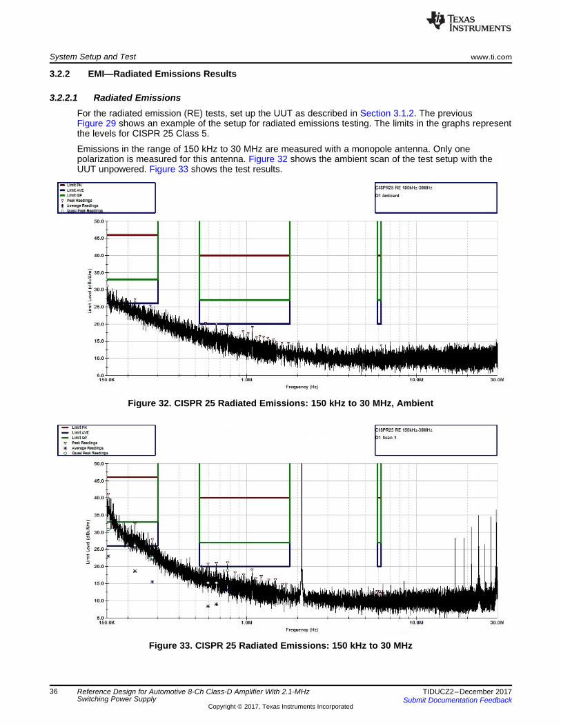
System Setup and Test www.ti.com
36 TIDUCZ2–December 2017Submit Documentation Feedback
Copyright © 2017, Texas Instruments Incorporated
Reference Design for Automotive 8-Ch Class-D Amplifier With 2.1-MHzSwitching Power Supply
3.2.2 EMI—Radiated Emissions Results
3.2.2.1 Radiated EmissionsFor the radiated emission (RE) tests, set up the UUT as described in Section 3.1.2. The previousFigure 29 shows an example of the setup for radiated emissions testing. The limits in the graphs representthe levels for CISPR 25 Class 5.
Emissions in the range of 150 kHz to 30 MHz are measured with a monopole antenna. Only onepolarization is measured for this antenna. Figure 32 shows the ambient scan of the test setup with theUUT unpowered. Figure 33 shows the test results.
Figure 32. CISPR 25 Radiated Emissions: 150 kHz to 30 MHz, Ambient
Figure 33. CISPR 25 Radiated Emissions: 150 kHz to 30 MHz

www.ti.com System Setup and Test
37TIDUCZ2–December 2017Submit Documentation Feedback
Copyright © 2017, Texas Instruments Incorporated
Reference Design for Automotive 8-Ch Class-D Amplifier With 2.1-MHzSwitching Power Supply
The radiated emissions average reading margin in the 150-kHz to 30-MHz range is greater than 3 dB forthe whole range.
Emissions in the range of 30 MHz to 200 MHz are measured with a biconical antenna in both horizontaland vertical polarizations. Figure 34 and Figure 35 show the ambient scans with the UUT power OFF.Figure 36 shows the results with the antenna horizontally polarized and Figure 37 shows the results withthe antenna vertically polarized.
Figure 34. CISPR 25 Radiated Emissions: 30 MHz to 200 MHz, Horizontal Antenna Orientation, AmbientScan
Figure 35. CISPR 25 Radiated Emissions: 30 MHz to 200 MHz, Vertical Antenna Orientation, Ambient Scan

System Setup and Test www.ti.com
38 TIDUCZ2–December 2017Submit Documentation Feedback
Copyright © 2017, Texas Instruments Incorporated
Reference Design for Automotive 8-Ch Class-D Amplifier With 2.1-MHzSwitching Power Supply
Figure 36. CISPR 25 Radiated Emissions: 30 MHz to 200 MHz, Horizontal Antenna Orientation
The radiated emissiongs average reading margin for the horizontal polarization test is greater than 13 dB.The peak reading margin is greater than 4 dB.
Figure 37. CISPR 25 Radiated Emissions: 30 MHz to 200 MHz, Vertical Antenna Orientation
The RE average reading margin for the vertical polarization test is greater than 5 dB. The peak readingmargin is greater than 6 dB.

www.ti.com System Setup and Test
39TIDUCZ2–December 2017Submit Documentation Feedback
Copyright © 2017, Texas Instruments Incorporated
Reference Design for Automotive 8-Ch Class-D Amplifier With 2.1-MHzSwitching Power Supply
Emissions in the frequency range from 200 MHz to 1000 MHz are measured with a horn antenna. Bothhorizontal and vertical polarizations of the antenna are tested. Figure 38 and Figure 39 show the ambientscan when the UUT power is OFF. Figure 40 and Figure 41 show the actual system response.
Figure 38. CISPR 25 Radiated Emissions: 200 MHz to 1 GHz, Horizontal Antenna Orientation, AmbientScan
Figure 39. CISPR 25 Radiated Emissions: 200 MHz to 1 GHz, Vertical Antenna Orientation, Ambient Scan

System Setup and Test www.ti.com
40 TIDUCZ2–December 2017Submit Documentation Feedback
Copyright © 2017, Texas Instruments Incorporated
Reference Design for Automotive 8-Ch Class-D Amplifier With 2.1-MHzSwitching Power Supply
Figure 40. CISPR 25 Radiated Emissions: 200 MHz to 1 GHz, Horizontal Antenna Orientation
The RE average reading margin for the horizontal polarization test is greater than 4 dB (see Figure 41).The peak reading reaches 26 dBµV at 200.6 MHz, which means that no margin is present at thatfrequency.
Figure 41. CISPR 25 Radiated Emissions: 200 MHz to 1 GHz, Vertical Antenna Orientation
The RE average reading margin for the vertical polarization test is greater than 6 dB. The peak readingmargin is greater than 2 dB.
The results show that the TIDA-00733 reference design can meet CISPR25 Class 5 radiated emissions.

www.ti.com Further EMI Design Considerations
41TIDUCZ2–December 2017Submit Documentation Feedback
Copyright © 2017, Texas Instruments Incorporated
Reference Design for Automotive 8-Ch Class-D Amplifier With 2.1-MHzSwitching Power Supply
4 Further EMI Design ConsiderationsEMI testing of the TIDA-00733 design led to several changes. The input filter and layout were changedsignificantly by shortening the distance from the box edge to the inductor L18. L18 was changed to a fully-shielded device to reduce signal pickup and subsequent radiation from the power lines. The value of L18was also lowered, which improved radiated emission readings.
Adding the small ferrites (R35, R36, R51, and R52) to the power connections on the PCM1865-Q1devices significantly reduced radiated emissions above 40 MHz. This reduction may be due to the lengthof the +3P3V routing. The ferrites reduce the amplitude of the higher frequencies that the PCM1865-Q1devices put on the +3P3V supply at the source of the noise.
Early tests led to adding C83 at power input T1; however, later testing indicated that this addition nolonger improves EMI performance, so it was de-populated.
Further improvements may be possible. Adding ferrites to the +3P3V power connections for U1, U2, andespecially U10, may further improve EMI performance. Increasing the value of L18 or C82 improves thelow-frequency EMI performance; however, the designer must take care to avoid impacting the higher-frequency EMI performance when making changes to L18 and C82. Creating a smaller board so that theTDM traces are shorter may also improve the EMI performance.

Design Files www.ti.com
42 TIDUCZ2–December 2017Submit Documentation Feedback
Copyright © 2017, Texas Instruments Incorporated
Reference Design for Automotive 8-Ch Class-D Amplifier With 2.1-MHzSwitching Power Supply
5 Design Files
5.1 SchematicsTo download the schematics, see the design files at TIDA-00733.
5.2 Bill of MaterialsTo download the bill of materials (BOM), see the design files at TIDA-00733.
5.3 PCB Layout RecommendationsThe TIDA-00733 PCB design was created to facilitate EMI testing and to reduce EMI effects. The TIDA-00733 PCB was laid out to fit into a metal box, a Hammond 1590J, which was machined to allow the endsof the board with the connectors to stick out. To fit the box well, the different groups of circuitry have beenspread out more than they would be in a size-optimized system. The box is intended to make contact withthe top and bottom surfaces of the PCB where the long gold strips are on each side of the board. Thisconfiguration creates a Faraday cage that encloses all of the active circuitry in the box while creatingconnections to the board ground.
The box lid is used as a heat sink for the TAS6424-Q1 components. The shorter support components forthe TAS6424-Q1 devices are placed near the TAS6424-Q1 devices on the bottom layer, while thecomponents taller than the TAS6424-Q1 devices are placed on the top of the board to provide clearancefor the lid or other heatsink.
Figure 42 shows the top layer of the PCB. Most components are on this layer. The circuits along the upperpart of the PCB are the power input filter and smart diode, the LM53635L-Q1 circuit, the LP5912-Q1circuit, and the MSP430. A connector for a +5-V load is on the right side of the board at the top. Theinductors, filter capacitors, and output connectors for the TAS6424-Q1 circuits are along the left side.Power routing for the PVDD connection of the TAS6424-Q1 devices is a wide trace near the center of theboard. Three mounting holes have been provided to attach the lid or other heat sink to the board. Theholes are spaced to provide even thermal connections across the thermal pad on the two TAS6424-Q1devices.
The input filter components are placed very close to the edge of the box to minimize the length of thepower trace from the power connector to the filter. The LM74610 smart diode circuit is next. The output ofthe LM74610 connects to a large area that includes the PVDD power connection for the LM53635-Q1 andthe two TAS6424-Q1 devices. The LM53635L-Q1 circuit is placed and routed to keep the current looparea small by placing the grounds of the circuit input and output capacitors close together. The routingfollows the recommendations specified in the LM53635-Q1 data sheet.
The two PCM1865-Q1 ADCs are in the lower right corner of the board just inside where the metal boxconnects to the board. The input components are placed very tightly together with the input connectorsoutside the enclosure area to the right. The test oscillator circuit, the LP5907-Q1 regulator, and theSN74LVC125A-Q1 hex buffer are placed just above the PCM1865-Q1 devices. The digital outputconnections are kept away from the analog inputs of the ADCs.

www.ti.com Design Files
43TIDUCZ2–December 2017Submit Documentation Feedback
Copyright © 2017, Texas Instruments Incorporated
Reference Design for Automotive 8-Ch Class-D Amplifier With 2.1-MHzSwitching Power Supply
Figure 42. TIDA-00733 Top Circuit Board—Top Layer
Figure 43 shows inner layer 1, which is below the top layer in the board stackup. This layer is primarily aground layer, though the input power connection and half of each audio output bridge are routed on thislayer to eliminate the possibility of a short circuit with the enclosure. These high-current connections allhave wide traces to ensure low losses in the board. Where a high current trace changes layers, multiplevias are used to reduce the impedance at the transition.
Figure 43. TIDA-00733 Circuit Board—Inner Layer 1

Design Files www.ti.com
44 TIDUCZ2–December 2017Submit Documentation Feedback
Copyright © 2017, Texas Instruments Incorporated
Reference Design for Automotive 8-Ch Class-D Amplifier With 2.1-MHzSwitching Power Supply
Figure 44 shows inner layer 2. This layer also has the input power connection and half of each audiooutput bridge are routed on it. This layer has the connection to the +5-V power connector and most of thesignal trace routing. The unused areas are covered with more ground.
Figure 44. TIDA-00733 Circuit Board—Inner Layer 2
Figure 45 shows the bottom layer of the board. As previously stated, the two TAS6424-Q1 devices areplaced on the bottom along with most of the small discrete components that form part of the circuit. Thelarge inductors required for 2-Ω operation make the overall dimensions for each TAS6424-Q1 circuitapproximately 34.6 mm × 42.7 mm.
Figure 45. TIDA-00733 Bottom Circuit Board Layer
5.3.1 Layout PrintsTo download the layer plots, see the design files at TIDA-00733.

www.ti.com Design Files
45TIDUCZ2–December 2017Submit Documentation Feedback
Copyright © 2017, Texas Instruments Incorporated
Reference Design for Automotive 8-Ch Class-D Amplifier With 2.1-MHzSwitching Power Supply
5.4 Altium ProjectTo download the Altium project files, see the design files at TIDA-00733.
5.5 Gerber FilesTo download the Gerber files, see the design files at TIDA-00733.
5.6 Assembly DrawingsTo download the assembly drawings, see the design files at TIDA-00733.
6 Software FilesTo download the software files, see the design files at TIDA-00733.
7 Related Documentation1. Texas Instruments, MIXED SIGNAL MICROCONTROLLER2. Texas Instruments, TAS6424-Q1 75-W, 2-MHz Digital Input 4-Channel Automotive Class-D Audio
Amplifier With Load-Dump Protection and I2C Diagnostics3. Texas Instruments, 2-MHz Automotive Class-D, 4-Channel, 21-W Audio Amplifier in Class-AB Form-
Factor Reference Design
7.1 TrademarksMSP430, PowerPAD, HotRod, Code Composer Studio, MSP430Ware are trademarks of TexasInstruments.All other trademarks are the property of their respective owners.
8 About the AuthorMARK KNAPP is a Systems Architect at Texas Instruments Incorporated who specializes in automotivepremium audio systems and instrument clusters. He also has an extensive background in video camerasystems and infrared imaging systems for military, automotive, and industrial applications. Mark earnedhis BSEE at the University of Michigan-Dearborn and his MSEE at the University of Texas at Dallas.

IMPORTANT NOTICE FOR TI DESIGN INFORMATION AND RESOURCES
Texas Instruments Incorporated (‘TI”) technical, application or other design advice, services or information, including, but not limited to,reference designs and materials relating to evaluation modules, (collectively, “TI Resources”) are intended to assist designers who aredeveloping applications that incorporate TI products; by downloading, accessing or using any particular TI Resource in any way, you(individually or, if you are acting on behalf of a company, your company) agree to use it solely for this purpose and subject to the terms ofthis Notice.TI’s provision of TI Resources does not expand or otherwise alter TI’s applicable published warranties or warranty disclaimers for TIproducts, and no additional obligations or liabilities arise from TI providing such TI Resources. TI reserves the right to make corrections,enhancements, improvements and other changes to its TI Resources.You understand and agree that you remain responsible for using your independent analysis, evaluation and judgment in designing yourapplications and that you have full and exclusive responsibility to assure the safety of your applications and compliance of your applications(and of all TI products used in or for your applications) with all applicable regulations, laws and other applicable requirements. Yourepresent that, with respect to your applications, you have all the necessary expertise to create and implement safeguards that (1)anticipate dangerous consequences of failures, (2) monitor failures and their consequences, and (3) lessen the likelihood of failures thatmight cause harm and take appropriate actions. You agree that prior to using or distributing any applications that include TI products, youwill thoroughly test such applications and the functionality of such TI products as used in such applications. TI has not conducted anytesting other than that specifically described in the published documentation for a particular TI Resource.You are authorized to use, copy and modify any individual TI Resource only in connection with the development of applications that includethe TI product(s) identified in such TI Resource. NO OTHER LICENSE, EXPRESS OR IMPLIED, BY ESTOPPEL OR OTHERWISE TOANY OTHER TI INTELLECTUAL PROPERTY RIGHT, AND NO LICENSE TO ANY TECHNOLOGY OR INTELLECTUAL PROPERTYRIGHT OF TI OR ANY THIRD PARTY IS GRANTED HEREIN, including but not limited to any patent right, copyright, mask work right, orother intellectual property right relating to any combination, machine, or process in which TI products or services are used. Informationregarding or referencing third-party products or services does not constitute a license to use such products or services, or a warranty orendorsement thereof. Use of TI Resources may require a license from a third party under the patents or other intellectual property of thethird party, or a license from TI under the patents or other intellectual property of TI.TI RESOURCES ARE PROVIDED “AS IS” AND WITH ALL FAULTS. TI DISCLAIMS ALL OTHER WARRANTIES ORREPRESENTATIONS, EXPRESS OR IMPLIED, REGARDING TI RESOURCES OR USE THEREOF, INCLUDING BUT NOT LIMITED TOACCURACY OR COMPLETENESS, TITLE, ANY EPIDEMIC FAILURE WARRANTY AND ANY IMPLIED WARRANTIES OFMERCHANTABILITY, FITNESS FOR A PARTICULAR PURPOSE, AND NON-INFRINGEMENT OF ANY THIRD PARTY INTELLECTUALPROPERTY RIGHTS.TI SHALL NOT BE LIABLE FOR AND SHALL NOT DEFEND OR INDEMNIFY YOU AGAINST ANY CLAIM, INCLUDING BUT NOTLIMITED TO ANY INFRINGEMENT CLAIM THAT RELATES TO OR IS BASED ON ANY COMBINATION OF PRODUCTS EVEN IFDESCRIBED IN TI RESOURCES OR OTHERWISE. IN NO EVENT SHALL TI BE LIABLE FOR ANY ACTUAL, DIRECT, SPECIAL,COLLATERAL, INDIRECT, PUNITIVE, INCIDENTAL, CONSEQUENTIAL OR EXEMPLARY DAMAGES IN CONNECTION WITH ORARISING OUT OF TI RESOURCES OR USE THEREOF, AND REGARDLESS OF WHETHER TI HAS BEEN ADVISED OF THEPOSSIBILITY OF SUCH DAMAGES.You agree to fully indemnify TI and its representatives against any damages, costs, losses, and/or liabilities arising out of your non-compliance with the terms and provisions of this Notice.This Notice applies to TI Resources. Additional terms apply to the use and purchase of certain types of materials, TI products and services.These include; without limitation, TI’s standard terms for semiconductor products http://www.ti.com/sc/docs/stdterms.htm), evaluationmodules, and samples (http://www.ti.com/sc/docs/sampterms.htm).
Mailing Address: Texas Instruments, Post Office Box 655303, Dallas, Texas 75265Copyright © 2017, Texas Instruments Incorporated
Related Documents


