The Pennsylvania State University The Graduate School Department of Mechanical and Nuclear Engineering DESIGN, FABRICATION, AND TESTING OF A PIEZOELECTRIC T-BEAM ACTUATOR A Thesis in Mechanical Engineering by Andrew D. Hirsh 2008 Andrew D. Hirsh Submitted in Partial Fulfillment of the Requirements for the Degree of Master of Science December 2008

Welcome message from author
This document is posted to help you gain knowledge. Please leave a comment to let me know what you think about it! Share it to your friends and learn new things together.
Transcript
The Pennsylvania State University
The Graduate School
Department of Mechanical and Nuclear Engineering
DESIGN, FABRICATION, AND TESTING OF A
PIEZOELECTRIC T-BEAM ACTUATOR
A Thesis in
Mechanical Engineering
by
Andrew D. Hirsh
2008 Andrew D. Hirsh
Submitted in Partial Fulfillment of the Requirements
for the Degree of
Master of Science
December 2008
The thesis of Andrew D. Hirsh was reviewed and approved* by the following:
Christopher D. Rahn Professor of Mechanical Engineering Thesis Co-Advisor
Srinivas A. Tadigadapa Associate Professor of Electrical Engineering Thesis Co-Advisor
Gary H. Koopmann, P.E. Distinguished Professor of Mechanical Engineering
Karen A. Thole Professor of Mechanical Engineering Head of the Department of Mechanical and Nuclear Engineering
*Signatures are on file in the Graduate School
iii
ABSTRACT
This thesis introduces a novel T-beam actuator fabricated using a precision dicing
saw. Bulk PZT is diced to produce cantilevered beams with T-shaped cross sections.
Electrodes are deposited on the top of the web, bottom of the flange, and the top of the
right and left flanges. Selectively activating these electrodes creates active and passive
regions in the PZT structure and in-plane and out-of-plane bending with bimorph-like
performance. Several devices are fabricated and experimentally tested for in-plane and
out-of-plane displacement using a microscope/camera with optical measurement.
Combinations of applied voltage, ground, and float on the four electrodes are tested to
determine optimal actuation cases that maximize tip deflection. For 19 mm long and 1
mm thick T-beam actuators, 15 microns of out-of-plane deflection amplitude and 5.5
microns of in-plane deflection amplitude is achieved at 0.4 V/micron actuation voltage.
iv
TABLE OF CONTENTS
LIST OF FIGURES .....................................................................................................v
LIST OF TABLES.......................................................................................................vii
ACKNOWLEDGEMENTS.........................................................................................viii
Chapter 1 Introduction ................................................................................................1
Chapter 2 T-Beam Concept ........................................................................................3
Chapter 3 Actuator Design & Device Fabrication......................................................5
3.1 Actuator Design ..............................................................................................5 3.2 Device Fabrication..........................................................................................7
Chapter 4 Experimental Setup and Testing ................................................................11
4.1 Experimental Setup.........................................................................................11 4.2 Device Characteristics ....................................................................................12 4.3 Device Testing ................................................................................................13 4.4 Results and Discussion ...................................................................................21
Chapter 5 Conclusions & Future Work ......................................................................23
Bibliography ................................................................................................................25
Appendix A Complete Experimental Data .................................................................27
Appendix B Cross Section Showing PZT Expansion Directions ...............................31
Appendix C Comparison with a MEMS Fabrication T-beam ....................................33
v
LIST OF FIGURES
Figure 2.1: T-beam concept: (a) as fabricated, and deflected shapes with a clamped left end and voltage is applied between (b) web and bottom electrode, (c) between flanges and bottom electrode, (d) left flange and bottom electrode, and (e) right flange and bottom electrode................................3
Figure 3.1: T-beam model: (a) the initial and deflected shape and (b) cross section ...................................................................................................................5
Figure 3.2: Fabricated T-beam Device 1 (t1 = 167.8 µm), Device 2 (t2 = 324.3 µm), Device 3 (t3 = 523.5 µm), Device 4 (t4 = 719.3 µm)....................................7
Figure 3.3: Packaged device with chrome/gold web/bottom electrodes and silver painted right and left flange electrodes.................................................................9
Figure 3.4: Back view of the packaged beam showing the 4 electrodes and the mount. ...................................................................................................................10
Figure 4.1: Virtual tip deflection test. ..........................................................................11
Figure 4.2: T-beam test cases. V = positive applied voltage, Solid arrow = motion direction, Dashed arrow = polarization direction, │ = floating electrode. Arrows inside structure indicate electric field. Maximum voltage is shown below each case. ...................................................................................................14
Figure 4.3: Device 1 upward out-of-plane actuation. Experimental results: ♦ = Case 1, ● = Case 2, ▲ = Case 3, ■ = Case 4........................................................15
Best fit lines: Solid = Case 1, Dashed = Case 2, Dotted = Case 3, Dash-Dot = Case 4....................................................................................................................15
Figure 4.4: Device 2 upward out-of-plane actuation. Experimental results: ♦ = Case 1, ● = Case 2, ▲ = Case 3, ■ = Case 4........................................................15
Best fit lines: Solid = Case 1, Dashed = Case 2, Dotted = Case 3, Dash-Dot = Case 4....................................................................................................................15
Figure 4.5: Device 3 upward out-of-plane actuation. Experimental results: ♦ = Case 1, ● = Case 2, ▲ = Case 3, ■ = Case 4........................................................16
Best fit lines: Solid = Case 1, Dashed = Case 2, Dotted = Case 3, Dash-Dot = Case 4....................................................................................................................16
Figure 4.6: Device 4 upward out-of-plane actuation. Experimental results: ♦ = Case 1, ● = Case 2, ▲ = Case 3, ■ = Case 4........................................................16
vi
Best fit lines: Solid = Case 1, Dashed = Case 2, Dotted = Case 3, Dash-Dot = Case 4....................................................................................................................16
Figure 4.7: Device 1 downward out-of-plane actuation. ............................................17
Experimental Results: ● = Case 5, ▲ = Case 6, ■ = Case 7. ......................................17
Best fit lines: Solid = Case 5, Dashed = Case 6, Dotted = Case 7...............................17
Figure 4.8: Device 2 downward out-of-plane actuation. ............................................18
Experimental Results: ● = Case 5, ▲ = Case 6, ■ = Case 7. ......................................18
Best fit lines: Solid = Case 5, Dashed = Case 6, Dotted = Case 7...............................18
Figure 4.9: Device 3 downward out-of-plane actuation. ............................................18
Experimental Results: ● = Case 5, ▲ = Case 6, ■ = Case 7. ......................................18
Best fit lines: Solid = Case 5, Dashed = Case 6, Dotted = Case 7...............................18
Figure 4.10: Device 4 downward out-of-plane actuation. ..........................................19
Experimental Results: ● = Case 5, ▲ = Case 6, ■ = Case 7. ......................................19
Best fit lines: Solid = Case 5, Dashed = Case 6, Dotted = Case 7...............................19
Figure 4.11: In-plane actuation. Symbol: ♦ = Device 1, ● = Device 2, ▲ = Device 3, ■ = Device 4. Open = left actuation (Case 8), Filled = right actuation (Case 9). ................................................................................................20
Best fit lines: Solid = Device 1, Dashed = Device 2, Dotted = Device 3, Dash-Dot = Device 4.............................................................................................................20
Figure 2.1: Cross-sectional view of PZT under applied voltages ................................31
Figure 2.2: Polarization vs. Electric Field hysteresis curve for 100µm thick PZT......32
Figure 3.1: T-beam MEMS fabrication process ..........................................................33
Figure 3.2: Photograph of the fabricated and mounted T-beam actuator with web and underside electrodes.......................................................................................34
Figure 3.3: Experimental actuator tip displacement w(L) vs. web voltage (V)...........35
Figure 3.4: Experimental actuator tip displacement w(L) vs. field (V/µm). Best fit slope value = 8.273 µm/(V/µm). ......................................................................36
vii
LIST OF TABLES
Table 3.1: Parameters for the T-beam actuator...........................................................8
Table 4.1: Device parameters (b=0.7 mm and s = 4.4 mm for all devices).................12
Table 4.2: Displacement vs. field slope values (µm/(V/µm)) for all devices and cases ......................................................................................................................20
Table 1.1: Device 1 displacement data .......................................................................27
Table 1.2: Device 2 displacement data .......................................................................28
Table 1.3: Device 3 displacement data .......................................................................29
Table 1.4: Device 4 displacement data .......................................................................30

viii
ACKNOWLEDGEMENTS
I would like to thank Dr. Chris Rahn for guiding me through my Master’s
research and for inspiring me to be the kind of professor he is. I would also like to thank
Dr. Srinivas Tadigadapa for advising my fabrication efforts and for pushing me beyond
what I thought I was capable of.
I would also like to thank my labmates, Kiron Mateti, Ashish Patwardhan,
Nicholas Duarte, Prasoon Joshi, Ping Kao, Bharadwaja Srowthi, and Siddharth Sonti for
all their wisdom and for making my graduate experience enjoyable.
I would also like to thank the National Science Foundation and the GREATT
Program for funding my graduate education and for instilling a love of teaching. The
students and teachers of Park Forest Middle School, Nittany Valley Charter School, Our
Lady Victory, and the Danville Correctional Facility will always be in my heart.
I would like to thank my family and friends for their love and encouragement. I
would not have made it without you. And thanks God for allowing me the opportunity to
show love and serve the people of State College during my graduate career.
Chapter 1
Introduction
Piezoelectric actuators are used for many applications, including precision-
positioning stages, ultra-fine focusing in optical equipment, and structural vibration
sensing and control. Piezoelectric ceramic actuators have desirable properties such as
high energy density, high bandwidth, and high force actuation. Most piezoelectric
actuators use lead zirconate titanate (PZT) as opposed to quartz or barium titanate due to
the greater electro-mechanical coupling coefficients and piezoelectric constants.
However, PZT exhibits a maximum strain of only ~0.1% and large motion is not possible
without strain amplification. Larger motion has been realized with stack actuators [1, 2,
3] which stack layers of PZT alternatively poled through the thickness connected to the
positive and negative terminals of a high voltage source. This interdigitated setup allows
the poling direction, electric field, and displacement to be in the same direction. The
stack actuator design takes advantage of the d33 piezoelectric constant which is larger
than the d31 constant (~ 1/3 of d33 ) used in unimorph or bimorph configurations. A
unimorph actuator has an active PZT layer poled through the thickness bonded to a
passive elastic layer [3, 4, 5, 6]. The active layer expands through the thickness and
contracts along the length to produce out-of-plane bending motion due to the offset
between the neutral axis and the center of the active layer due to the passive layer. A
bimorph actuator replaces the passive layer with another active layer and allows for
maximum transverse displacement because each layer can be activated with the
2
maximum field in the direction of poling. The field opposite the poling direction is
limited to ~ 1/3 the maximum field in the direction of poling so that the PZT will not
depole. PZT and PZN-PT based unimorph actuators have been fabricated and shown to
produce large out-of-plane motion for use in a micromechanical flapping mechanism
[11]. In-plane strain-amplifying piezoelectric actuators have been demonstrated with low
voltage/low displacement [12, 13, 14]. A serpentine-style design [15, 16] has been
developed to amplify the displacement for unimorph and bimorph actuators.
At the microscale, stack and unimorph/bimorph actuators are difficult to fabricate.
Although solder bonding techniques for PZT have been shown [7], stack actuators of
more than a few layers have not been fabricated. Unimorph actuators have been made [4,
8] using low performance ZnO and AlN. Thin film PZT has also been used in these
actuators but lacks the quality of bulk PZT [9] and stress mismatch between the layers
during fabrication results in variably deformed structures upon release. Tube actuators
that can produce bimorph actuation in two directions have been demonstrated at the 1-10
mm scale [10].
This thesis describes a new type of monolithic actuator fabricated from bulk PZT
using a high precision dicing saw. Using this method, a T-shaped two-axis bimorph
actuator can be machined and experimentally shown to produce both out-of-plane and in-
plane motion. Optimal application of voltage to the T-beam electrodes is developed that
maximizes displacement.
Chapter 2
T-Beam Concept
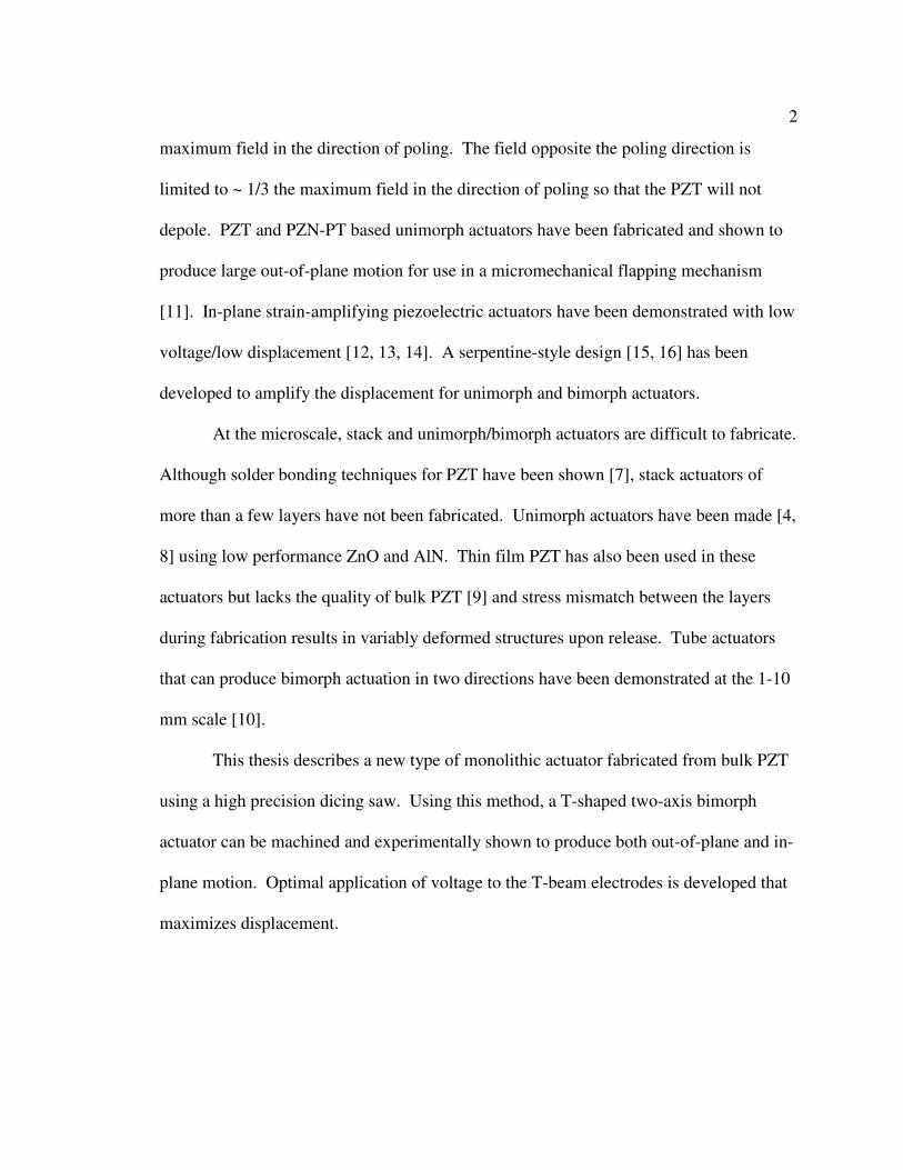
The T-beam actuator can provide bimorph actuation in two directions as shown in
Figure 2.1. The T-beam actuator is cantilevered and has a T-shaped cross section. The
entire T-beam is bulk PZT with electrodes deposited on the top of the web, the top of
each flange, and the bottom of the flange. The PZT is poled through the thickness from
top to bottom.
Figure 2.1: T-beam concept: (a) as fabricated, and deflected shapes with a clamped left end and voltage is applied between (b) web and bottom electrode, (c) between flanges and bottom electrode, (d) left flange and bottom electrode, and (e) right flange and bottom electrode.
4
Figure 2.1 shows how the T-beam actuator can be bent both in-plane and out-of-
plane by selectively activating the electrodes. The web or flange sections can either
expand or contract longitudinally through the d31 piezoelectric effect. The active part of
the structure (web/flange) either expands or contracts longitudinally while the passive
part (flange/web, respectively) acts to constrain the T-beam and effectively creates a
unimorph actuator. Out-of-plane upward displacement can be achieved by applying a
field that either contracts the web section only (unimorph), expands the two flanges only
(unimorph), or both (bimorph) to further increase displacement (see Figure 2.1(b)) . Out-
of-plane downward displacement can be achieved either by expanding the web section
only (unimorph), contracting the two flanges only (unimorph), or both (bimorph) (see
Figure 2.1(c)).
It is desirable to activate the structure at its maximum electric field, EMAX, in the
direction of poling. The maximum field opposite the direction of poling, however, is
typically limited to 1/3 EMAX so as not to depole the structure. Hence, the bimorph T-
beam design with maximum field applied for both upward and downward motion
provides much larger displacement than with a single active layer (unimorph).
The T-beam can also provide in-plane displacement by differential application of
voltage on the two flanges. To bend left as shown in Figure 2.1(d), the left flange
electrode is actuated at EMAX and the right flange electrode can either be passive and
provide unimorph actuation or active at -1/3 EMAX. To bend right, the left and right
flange electrode fields are switched (see Figure 2.1(e)).
Chapter 3
Actuator Design & Device Fabrication
3.1 Actuator Design
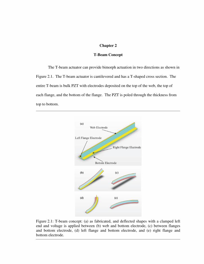
The T-beam model developed by Kommepalli et al. [11] show that the T-beam
geometry can be optimized to produce maximum displacement. Figure 3.1 shows the
cross section used in the modeling with controllable fabrication parameters flange width
s, flange thickness t, web thickness b, and (fixed) overall thickness h.
The T-beam is modeled as a cantilever beam using Euler-Bernoulli beam theory.
Voltage is applied between the web (VW) or the two flange electrodes (VG) and bottom
electrode. VW and VG are assumed to produce uniform uni-axial electric fields only in
Figure 3.1: T-beam model: (a) the initial and deflected shape and (b) cross section
6
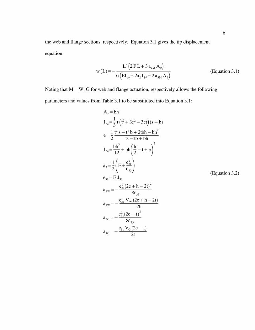
the web and flange sections, respectively. Equation 3.1 gives the tip displacement
equation.
Noting that M = W, G for web and flange actuation, respectively allows the following
parameters and values from Table 3.1 to be substituted into Equation 3.1:
w L` a
=@
L2 2 F L + 3 a4M A p
b c
6 EI be + 2a2 I pe + 2 a3M A p
b cffffffffffffffffffffffffffffffffffffffffffffffffffffffffffffffffffffffffffffffffffffff (Equation 3.1)
A p = bh
I be =13ffft t2
+ 3e2@ 3et
b c
s@ b` a
e =12ffft2 s@ t2 b + 2tbh@ bh2
ts@ tb + bhffffffffffffffffffffffffffffffffffffffffffffffffffffffffffffffffffffff
I pe =bh3
12ffffffffff
+ bhh2ffff
@ t + ef g2
a2 =12fffE +
e312
ε33
ffffffff
h
j
i
k
e31 = Ed31
a3W =@e31
2 2e + h@ 2t` a2
8ε33
fffffffffffffffffffffffffffffffffffffffffffffffffff
a4W =@e31 VW 2e + h@ 2t
` a
2hfffffffffffffffffffffffffffffffffffffffffffffffffffffffffffff
a3G =@e31
2 2e@ t` a2
8ε33
fffffffffffffffffffffffffffffffffff
a4G =@e31 VG 2e@ t
` a
2tffffffffffffffffffffffffffffffffffffffffffff
(Equation 3.2)
7
3.2 Device Fabrication
The T-beam actuators are fabricated using a Kulicke & Soffa Industries Model
980 precision dicing saw. T-beams with different parameters (t, s, b) can quickly be
fabricated and tested because they are simple to dice from bulk PZT (Boston Piezo Optics
(BPO) Navy Type I, PZT-4) and electrode. The process starts with 1” x 1” x 1 mm bulk
PZT with chrome/gold electrodes on both sides and poled through the thickness. The
chip is mounted on a 4” Si wafer using 1827 photoresist for stability during machining.
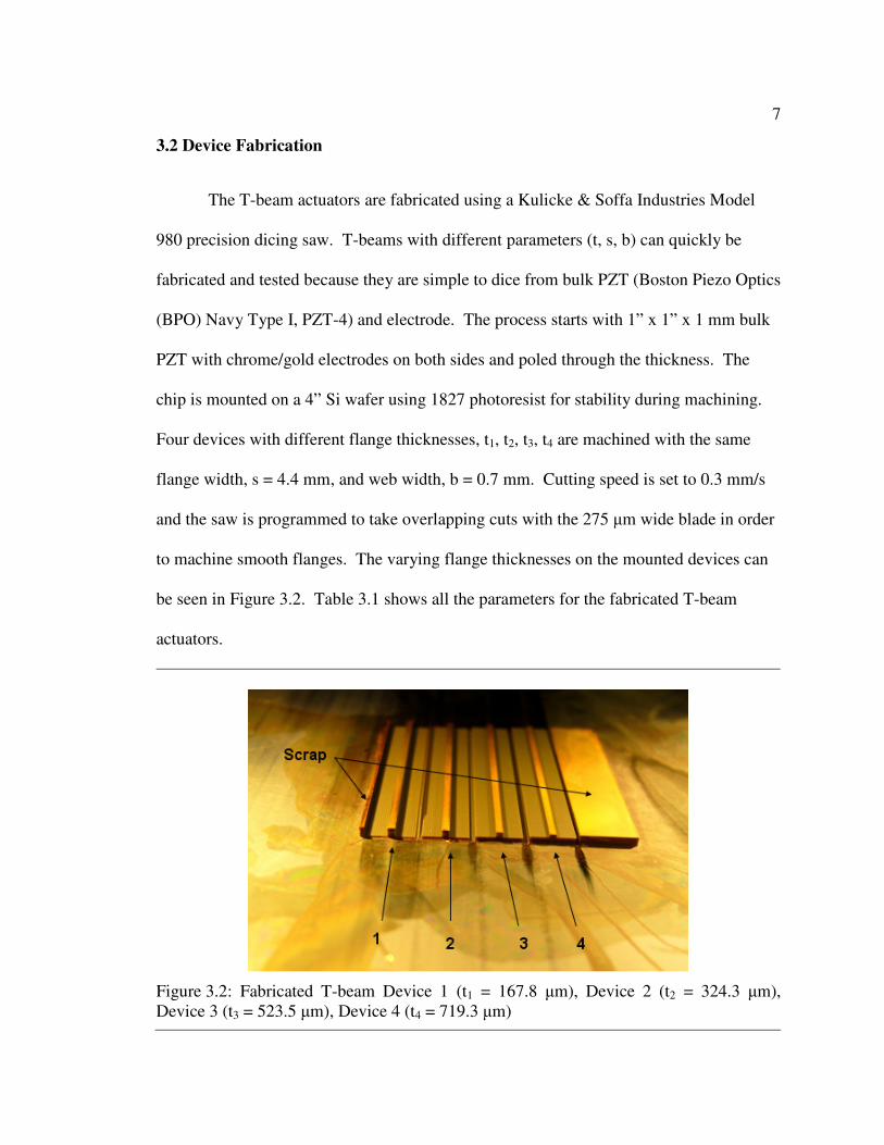
Four devices with different flange thicknesses, t1, t2, t3, t4 are machined with the same
flange width, s = 4.4 mm, and web width, b = 0.7 mm. Cutting speed is set to 0.3 mm/s
and the saw is programmed to take overlapping cuts with the 275 µm wide blade in order
to machine smooth flanges. The varying flange thicknesses on the mounted devices can
be seen in Figure 3.2. Table 3.1 shows all the parameters for the fabricated T-beam
actuators.
Figure 3.2: Fabricated T-beam Device 1 (t1 = 167.8 µm), Device 2 (t2 = 324.3 µm), Device 3 (t3 = 523.5 µm), Device 4 (t4 = 719.3 µm)
8
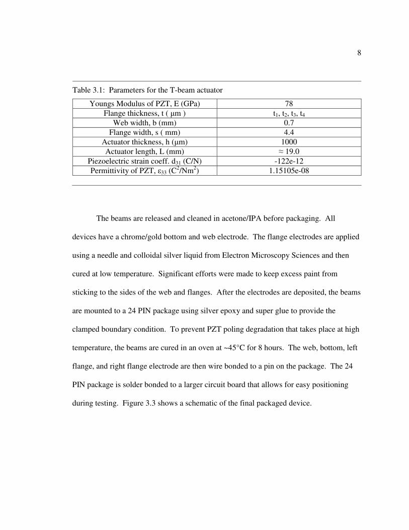
The beams are released and cleaned in acetone/IPA before packaging. All
devices have a chrome/gold bottom and web electrode. The flange electrodes are applied
using a needle and colloidal silver liquid from Electron Microscopy Sciences and then
cured at low temperature. Significant efforts were made to keep excess paint from
sticking to the sides of the web and flanges. After the electrodes are deposited, the beams
are mounted to a 24 PIN package using silver epoxy and super glue to provide the
clamped boundary condition. To prevent PZT poling degradation that takes place at high
temperature, the beams are cured in an oven at ~45°C for 8 hours. The web, bottom, left
flange, and right flange electrode are then wire bonded to a pin on the package. The 24
PIN package is solder bonded to a larger circuit board that allows for easy positioning
during testing. Figure 3.3 shows a schematic of the final packaged device.
Table 3.1: Parameters for the T-beam actuator
Youngs Modulus of PZT, E (GPa) 78 Flange thickness, t ( µm ) t1, t2, t3, t4
Web width, b (mm) 0.7 Flange width, s ( mm) 4.4
Actuator thickness, h (µm) 1000 Actuator length, L (mm) ≈ 19.0
Piezoelectric strain coeff. d31 (C/N) -122e-12 Permittivity of PZT, ε33 (C
2/Nm2) 1.15105e-08
9
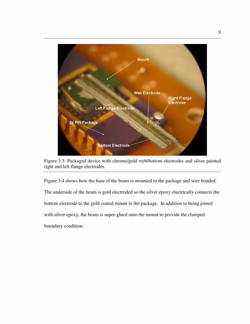
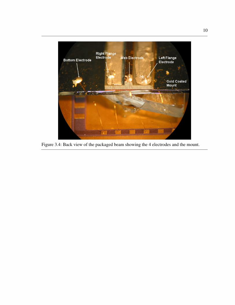
Figure 3.4 shows how the base of the beam is mounted to the package and wire bonded.
The underside of the beam is gold electroded so the silver epoxy electrically connects the
bottom electrode to the gold coated mount in the package. In addition to being joined
with silver epoxy, the beam is super-glued onto the mount to provide the clamped
boundary condition.
Figure 3.3: Packaged device with chrome/gold web/bottom electrodes and silver painted right and left flange electrodes.
10
Figure 3.4: Back view of the packaged beam showing the 4 electrodes and the mount.
Chapter 4
Experimental Setup and Testing
4.1 Experimental Setup
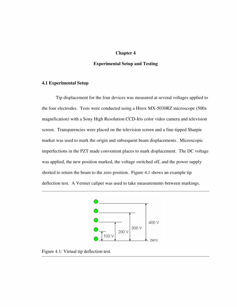
Tip displacement for the four devices was measured at several voltages applied to
the four electrodes. Tests were conducted using a Hirox MX-5030RZ microscope (500x
magnification) with a Sony High Resolution CCD-Iris color video camera and television
screen. Transparencies were placed on the television screen and a fine-tipped Sharpie
marker was used to mark the origin and subsequent beam displacements. Microscopic
imperfections in the PZT made convenient places to mark displacement. The DC voltage
was applied, the new position marked, the voltage switched off, and the power supply
shorted to return the beam to the zero position. Figure 4.1 shows an example tip
deflection test. A Vernier caliper was used to take measurements between markings.
Figure 4.1: Virtual tip deflection test.
12
A calibration factor was used to convert physical transparency measurements to actual
micrometer beam tip displacements. The thickness of a glass slide was used as the
calibration standard and measured to be 151µm with a micrometer with 1 µm precision.
The glass slide measured 90.0 mm on the screen transparency so the scale factor of
151µm/90.0mm was used.
This testing method produced repeatable measurements with small error. The
largest source of error was the diameter of the pen markings which were approximately
0.5mm. Converted to displacement measurements, the measurement uncertainty is less
than a micron.
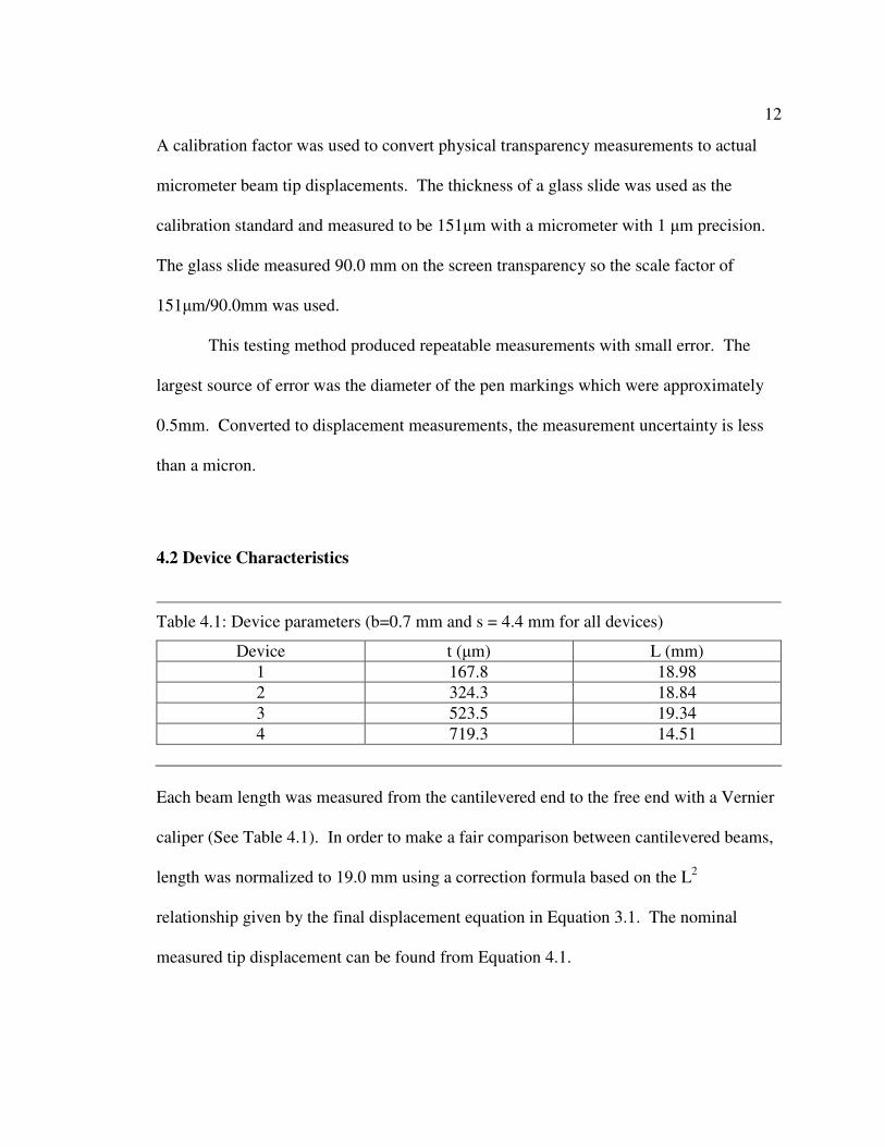
4.2 Device Characteristics
Each beam length was measured from the cantilevered end to the free end with a Vernier
caliper (See Table 4.1). In order to make a fair comparison between cantilevered beams,
length was normalized to 19.0 mm using a correction formula based on the L2
relationship given by the final displacement equation in Equation 3.1. The nominal
measured tip displacement can be found from Equation 4.1.
Table 4.1: Device parameters (b=0.7 mm and s = 4.4 mm for all devices)
Device t (µm) L (mm) 1 167.8 18.98 2 324.3 18.84 3 523.5 19.34 4 719.3 14.51
13
4.3 Device Testing
This study seeks to find the combinations of +V, ground, and float applied to the
four electrodes that maximizes out-of-plane and in-plane displacement. Although it is
possible to provide large field in the direction of poling, the actuator displacement
saturates and significant field increases do not yield increased displacement. It was
observed on a test device that ~550V (E = 0.55V/µm) applied between the bottom and
web electrode (h = 1 mm) opposite the direction of poling was enough to depole the
material. In this study, the field is calculated as the applied voltage divided by the
minimum separation between the electrodes. An arbitrary low field, EMAX = 0.4 V/µm, is
used to ensure that the material does not depole or arcs do not occur between electrodes.
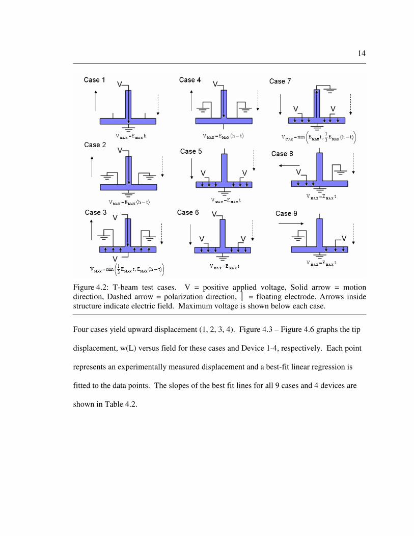
The voltage application cases are shown in Figure 4.2. The desired direction of
motion, polarization direction, electric field, and maximum applied voltage are shown.
Cases 1-4 yield upward out-of-plane displacement, Cases 5-7 yield downward out-of-
plane displacement, and Cases 8-9 yield in-plane displacement. The maximum voltages
are geometry dependent, and hence, device dependent. In addition to limiting the field in
the polarization direction, the field opposite the direction of poling is maintained to be
less than 1/3 EMAX. In Cases 3 and 7, the applied voltage depends on the flange thickness
to ensure that the field is neither too great in the web nor the flange.
wmeas
Lnominal
Lactual
fffffffffffffffffffff
h
j
i
k
2
= w measnominal (Equation 4.1)
14
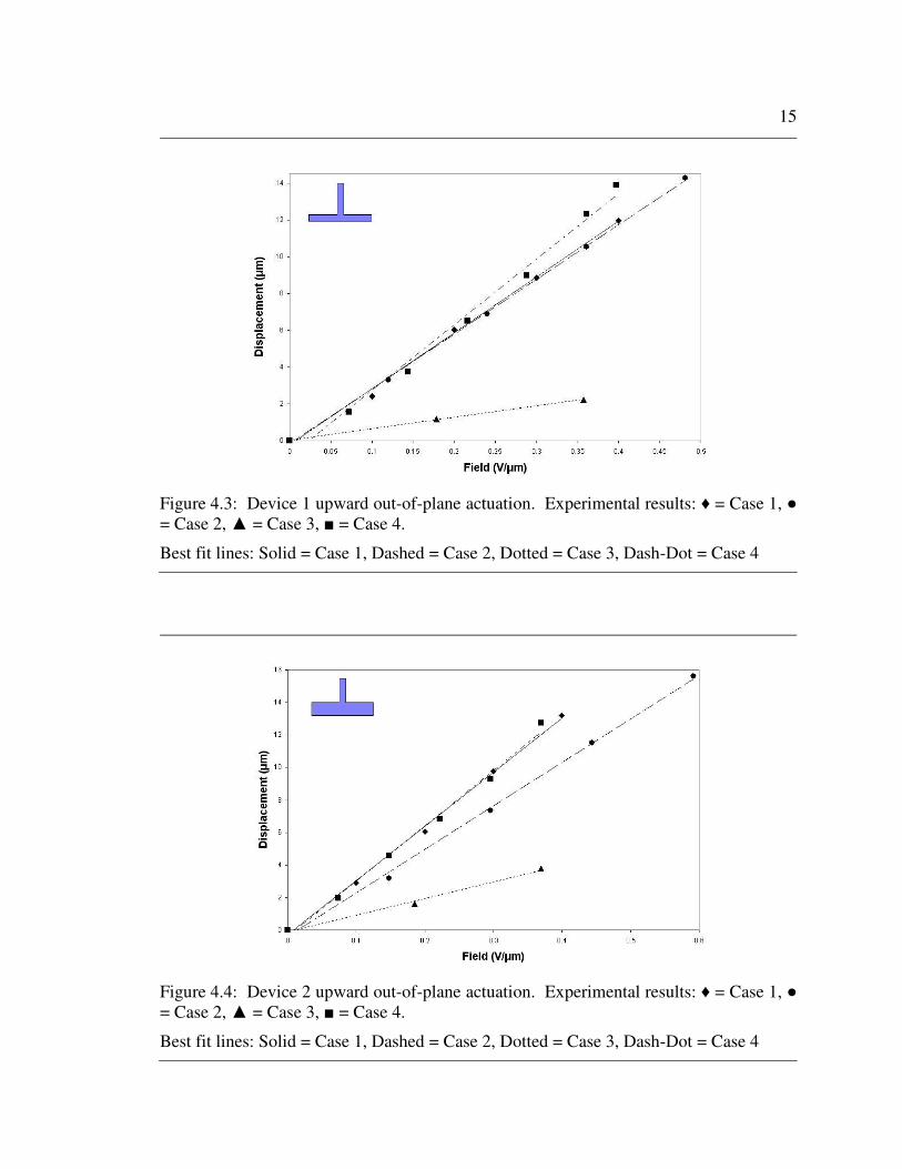
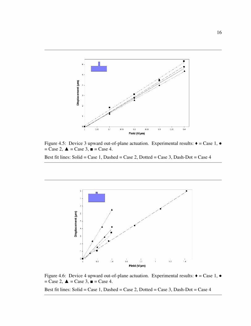
Four cases yield upward displacement (1, 2, 3, 4). Figure 4.3 – Figure 4.6 graphs the tip
displacement, w(L) versus field for these cases and Device 1-4, respectively. Each point
represents an experimentally measured displacement and a best-fit linear regression is
fitted to the data points. The slopes of the best fit lines for all 9 cases and 4 devices are
shown in Table 4.2.
Figure 4.2: T-beam test cases. V = positive applied voltage, Solid arrow = motion direction, Dashed arrow = polarization direction, │ = floating electrode. Arrows inside structure indicate electric field. Maximum voltage is shown below each case.
15
Figure 4.3: Device 1 upward out-of-plane actuation. Experimental results: ♦ = Case 1, ● = Case 2, ▲ = Case 3, ■ = Case 4.
Best fit lines: Solid = Case 1, Dashed = Case 2, Dotted = Case 3, Dash-Dot = Case 4
Figure 4.4: Device 2 upward out-of-plane actuation. Experimental results: ♦ = Case 1, ● = Case 2, ▲ = Case 3, ■ = Case 4.
Best fit lines: Solid = Case 1, Dashed = Case 2, Dotted = Case 3, Dash-Dot = Case 4
16
Figure 4.5: Device 3 upward out-of-plane actuation. Experimental results: ♦ = Case 1, ● = Case 2, ▲ = Case 3, ■ = Case 4.
Best fit lines: Solid = Case 1, Dashed = Case 2, Dotted = Case 3, Dash-Dot = Case 4
Figure 4.6: Device 4 upward out-of-plane actuation. Experimental results: ♦ = Case 1, ● = Case 2, ▲ = Case 3, ■ = Case 4.
Best fit lines: Solid = Case 1, Dashed = Case 2, Dotted = Case 3, Dash-Dot = Case 4
17
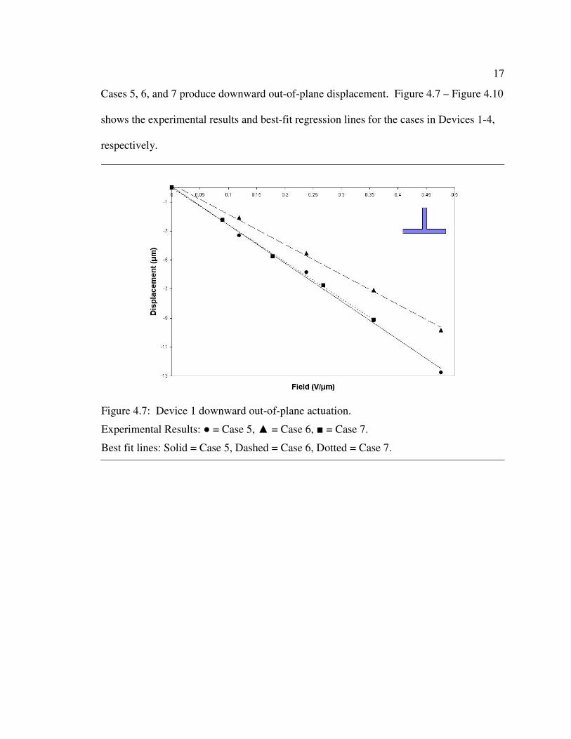
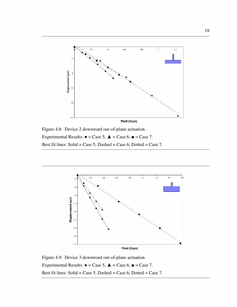
Cases 5, 6, and 7 produce downward out-of-plane displacement. Figure 4.7 – Figure 4.10
shows the experimental results and best-fit regression lines for the cases in Devices 1-4,
respectively.
Figure 4.7: Device 1 downward out-of-plane actuation.
Experimental Results: ● = Case 5, ▲ = Case 6, ■ = Case 7.
Best fit lines: Solid = Case 5, Dashed = Case 6, Dotted = Case 7.
18
Figure 4.8: Device 2 downward out-of-plane actuation.
Experimental Results: ● = Case 5, ▲ = Case 6, ■ = Case 7.
Best fit lines: Solid = Case 5, Dashed = Case 6, Dotted = Case 7.
Figure 4.9: Device 3 downward out-of-plane actuation.
Experimental Results: ● = Case 5, ▲ = Case 6, ■ = Case 7.
Best fit lines: Solid = Case 5, Dashed = Case 6, Dotted = Case 7.
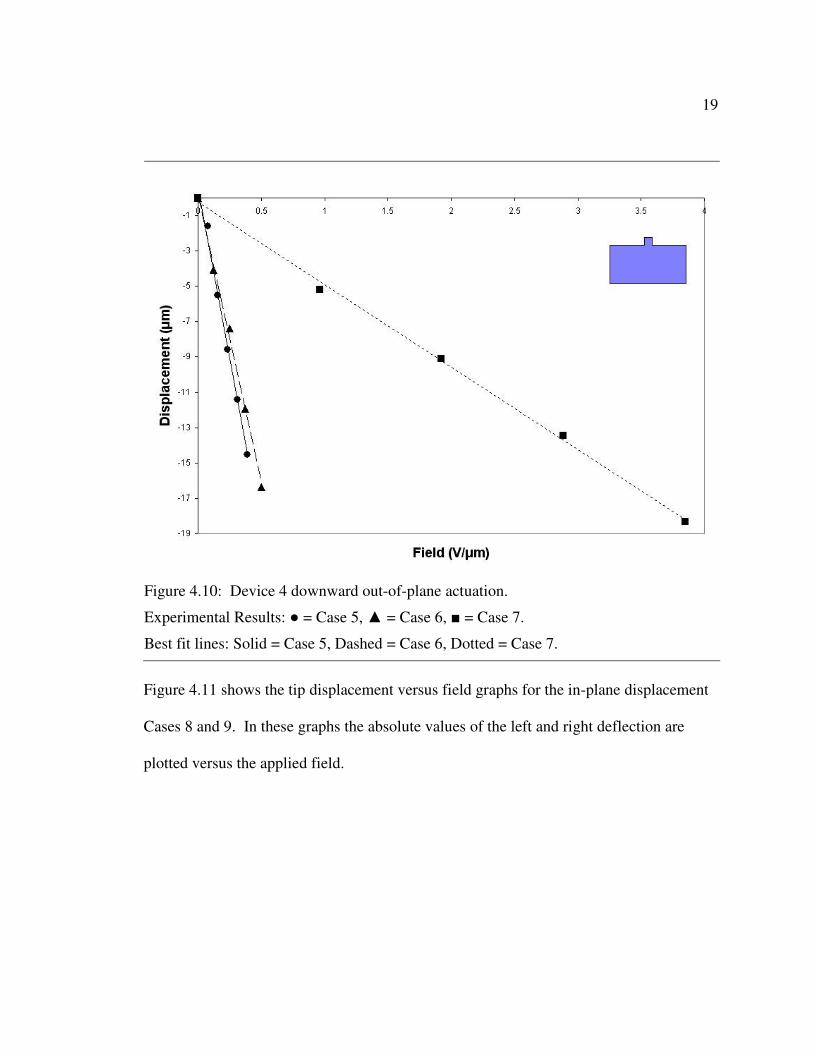
19
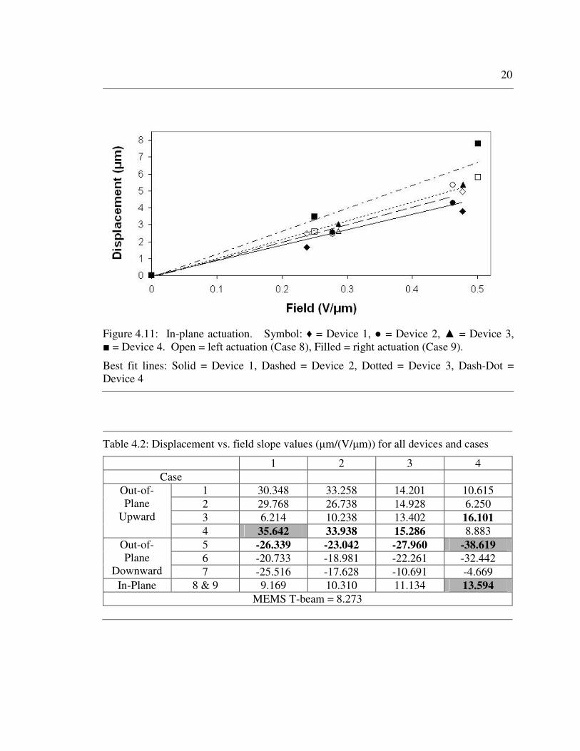
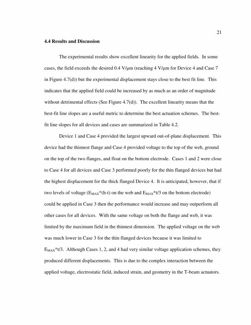
Figure 4.11 shows the tip displacement versus field graphs for the in-plane displacement
Cases 8 and 9. In these graphs the absolute values of the left and right deflection are
plotted versus the applied field.
Figure 4.10: Device 4 downward out-of-plane actuation.
Experimental Results: ● = Case 5, ▲ = Case 6, ■ = Case 7.
Best fit lines: Solid = Case 5, Dashed = Case 6, Dotted = Case 7.
20
Figure 4.11: In-plane actuation. Symbol: ♦ = Device 1, ● = Device 2, ▲ = Device 3, ■ = Device 4. Open = left actuation (Case 8), Filled = right actuation (Case 9).
Best fit lines: Solid = Device 1, Dashed = Device 2, Dotted = Device 3, Dash-Dot = Device 4
Table 4.2: Displacement vs. field slope values (µm/(V/µm)) for all devices and cases
1 2 3 4 Case
1 30.348 33.258 14.201 10.615 2 29.768 26.738 14.928 6.250 3 6.214 10.238 13.402 16.101
Out-of-Plane
Upward 4 35.642 33.938 15.286 8.883 5 -26.339 -23.042 -27.960 -38.619
6 -20.733 -18.981 -22.261 -32.442 Out-of-Plane
Downward 7 -25.516 -17.628 -10.691 -4.669 In-Plane 8 & 9 9.169 10.310 11.134 13.594
MEMS T-beam = 8.273
21
4.4 Results and Discussion
The experimental results show excellent linearity for the applied fields. In some
cases, the field exceeds the desired 0.4 V/µm (reaching 4 V/µm for Device 4 and Case 7
in Figure 4.7(d)) but the experimental displacement stays close to the best fit line. This
indicates that the applied field could be increased by as much as an order of magnitude
without detrimental effects (See Figure 4.7(d)). The excellent linearity means that the
best-fit line slopes are a useful metric to determine the best actuation schemes. The best-
fit line slopes for all devices and cases are summarized in Table 4.2.
Device 1 and Case 4 provided the largest upward out-of-plane displacement. This
device had the thinnest flange and Case 4 provided voltage to the top of the web, ground
on the top of the two flanges, and float on the bottom electrode. Cases 1 and 2 were close
to Case 4 for all devices and Case 3 performed poorly for the thin flanged devices but had
the highest displacement for the thick flanged Device 4. It is anticipated, however, that if
two levels of voltage (EMAX*(h-t) on the web and EMAX*t/3 on the bottom electrode)
could be applied in Case 3 then the performance would increase and may outperform all
other cases for all devices. With the same voltage on both the flange and web, it was
limited by the maximum field in the thinnest dimension. The applied voltage on the web
was much lower in Case 3 for the thin flanged devices because it was limited to
EMAX*t/3. Although Cases 1, 2, and 4 had very similar voltage application schemes, they
produced different displacements. This is due to the complex interaction between the
applied voltage, electrostatic field, induced strain, and geometry in the T-beam actuators.
22
Device 4 and Case 5 produced the largest downward out-of-plane displacement.
In this case, voltage was applied to the top of the flange, the bottom electrode was
grounded, and the web electrode floated. It is interesting to note that Case 7 in the thin
flanged Device 1 did not produce more displacement than Case 5 and 6. The web was
reverse biased, presumably leading to larger out-of-plane displacement than Cases 5 and
6. Again, the chose of floating or ground electrodes led to significantly different
performance due to the complex electromechanics of the T-beam actuator.
The maximum in-plane displacement occurred in Device 4. This device has the
thickest flange and hence more active material relative to the passive web. The best-fit
linear regression is fitted to both left and right actuation (4 data points). The differences
in right and left deflection arise from slightly different right and left flange widths during
fabrication.
Chapter 5
Conclusions & Future Work
This thesis shows that T-beam actuators demonstrate bimorph actuation in two
directions using a monolithic PZT structure. The T-beam actuators are fabricated using
simple dicing and electrode application. Selective application of voltage, float, and
ground to the four T-beam electrodes creates bending upward, downward, left, and right.
Applied voltage limits are postulated based on the maximum allowable field in the PZT
and minimum distances between the electrodes. The T-beam devices exhibit linear
displacement for applied voltages up to 0.4 V/µm. The slopes of the displacement versus
field best-fit lines are used to compare voltage application schemes. It is found that
thinner flanges produce more out-of-plane displacement and thicker flanges produce
more in-plane displacement. Reverse-biasing the inactive material was not found to
improve displacement.
T-beam actuators suffer from the same limitations as bi-morph actuators. Long
and thin beams are needed to produce large displacements. The fabricated T-beam
devices, having actuator lengths of ~19mm, provided displacements of only ~10-20µm
using upwards of 400V. For comparison, a 100µm thick MEMS fabricated T-beam (See
Appendix C and Figure 3.3), at only 8mm long, provided 21µm displacement at 270V,
despite having a low slope value in Table 4.2. Thus, using MEMS fabrication and thin
PZT has the potential to provide large displacements at low voltages.

24
Future work will continue to develop designs taking advantage of MEMS
fabrication. Testing the devices at higher field will also be necessary to maximize
actuator performance. Retesting these four devices and measuring the induced voltage on
the floating electrode would also be of interest. Modeling of the electromechanics of T-
beams has the potential to explain the counter-intuitive results observed in the
experiments.
Bibliography
1. Giurgiutiu, V., and Rogers, C.A., 1996. “Energy based comparison of solid state induced strain actuators”. Journal of Intelligent Material Systems and Structures, 7, January, pp. 4-14.
2. Giurgiutiu, V., Rogers, C.A., and Chaudhry, Z., 1997. “Design of displacement amplified induced-strain actuators for maximum energy output”. Journal of
Mechanical Design, 119, December, pp. 511-517.
3. Uchino, K., 2003. Micromechatronics. Marcel Dekker, New York.
4. Percin, G., 2001. “Micromachined piezoelectrically actuated flextensional transducers for high resolution printing and imaging”. IEEE Ultrasonics
Symposium, pp. 921-924.
5. Basak, S., Raman, A., and Garimella, S. V., 2005. “Dynamic response optimization of piezoelectrically excited thin resonant beams”. Journal of
Vibration and Acoustics, 127, pp. 18-27.
6. Wang, Q.-M., Du, X.-H., Xu, B., and Cross, L. E., 1999. “Electromechanical coupling and output efficiency of piezoelectric bending actuators”. IEEE Transactions on Ultrasonics, Ferroelectrics, and Frequency Control, 46(3), pp. 638-646.
7. Goyal, A., Cheong, J., and Tadigadapa, S. A., 2004. “Tin-based solder bonding for mems fabrication and packaging applications”. Journal of Micromechanics
and Microengineering, 14(6), June, pp. 819-825.
8. Cheong, J., Tadigadapa, S. A., and Rahn, C. D., 2005. “Fabrication and performance of a flextensional microactuator”. Journal of Micromechanics and
Microengineering, 15, pp. 1947-1955.
9. Gross, S. J., Tadigadapa, S. A., Jackson, T. N., Trolier-McKinstry, S., and Zhang, Q. Q., 2003. “Lead-zirconate-titanate based piezoelectric micromachined switch”. Applied Physics Letters, 83(1), July, pp. 174-176.
10. Berg, M., Hagedorn, P., and Gutschmidt, S., 2004. “On the dynamics of piezoelectric cylindrical shells”. Journal of Sound and Vibration, 274(1-2), July, pp. 91-109.
26
11. Kommepalli, H. K. R., Hirsh, A. D., Rahn, C. D., and Tadigadapa, S. A., 2008. “Piezoelectric T-beam microactuators”. Proceedings of ASME International
Design Engineering Technical Conferences, August, pp. 1-6.
12. Sitti, M., Campolo, D., Yan, J., Fearing, R. S., Su, T., Taylor, D., and Sands, T., 2001. “Development of PZT and PZN-PT based unimorph actuators for micromechanical flapping mechanisms”. IEEE Conference on Robotics and
Automation, May, pp. 3839-3846.
13. Conway, N. J., Traina, Z. J., and Kim, S.-G., 2007. “A strain amplifying piezoelectric MEMS actuator”. Journal of Micromechanics and
Microengineering, 17(2007), March, pp. 781-787.
14. Lee, T.-M., Seo, Y. H., Whang, K.-H., and Choi, D.-S., 2006. “Study on the lateral piezoelectric actuator with actuation range amplifying structure”. Trans
Tech Publications, Switzerland, December, pp. 1-4.
15. Seo, Y. H., Choi, D.-S., Lee, J.-H., Je, T.-J., and Whang, K.-H., 2005. “Laterally driven thin film PZT actuator with high-aspect-ratio silicon beam for stroke amplification”. Sensors and Actuators A, 127(2006), November, pp. 302-309.
16. Fang, H., Liu, L., and Ren, T., 2006. “Modeling and design optimization of large-deflection piezoelectric folded cantilever microactuators”. IEEE Transactions on Ultrasonics, Ferroelectrics, and Frequency Control, 53(1), January, pp. 237-240.
Appendix A
Complete Experimental Data
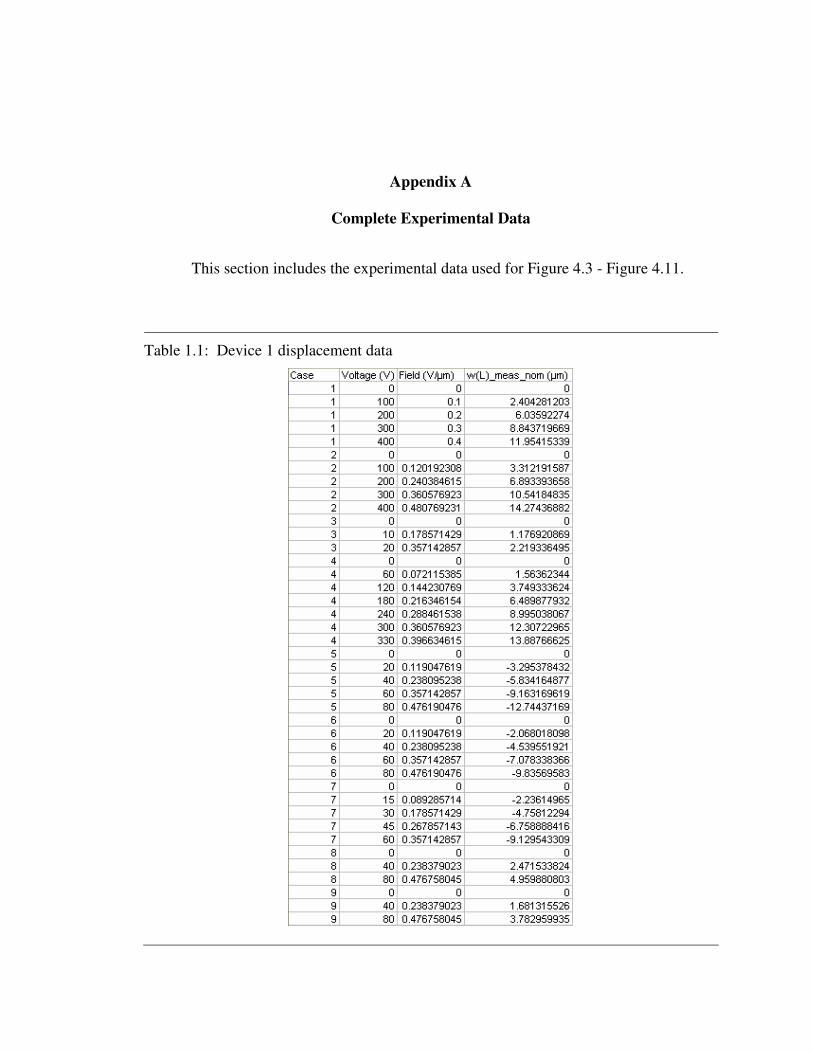
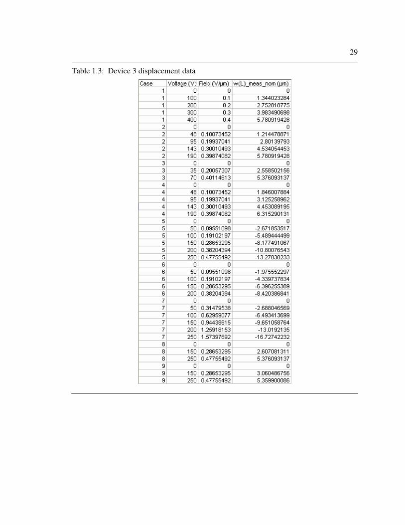
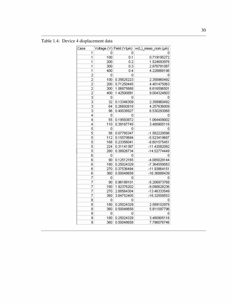
This section includes the experimental data used for Figure 4.3 - Figure 4.11.
Table 1.1: Device 1 displacement data
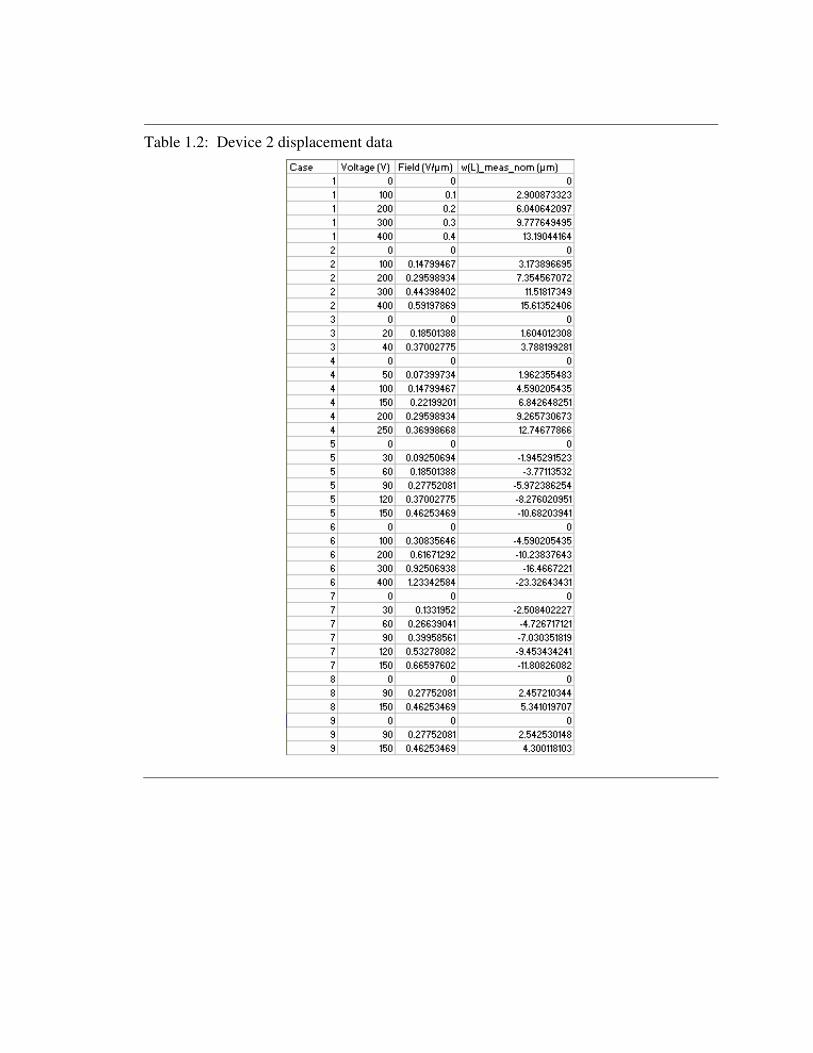
Table 1.2: Device 2 displacement data
29
Table 1.3: Device 3 displacement data
30
Table 1.4: Device 4 displacement data
Appendix B
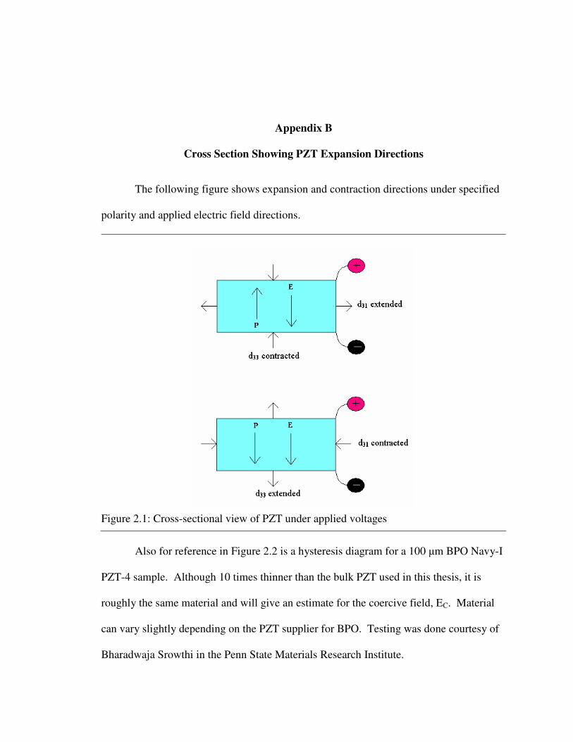
Cross Section Showing PZT Expansion Directions
The following figure shows expansion and contraction directions under specified
polarity and applied electric field directions.
Also for reference in Figure 2.2 is a hysteresis diagram for a 100 µm BPO Navy-I
PZT-4 sample. Although 10 times thinner than the bulk PZT used in this thesis, it is
roughly the same material and will give an estimate for the coercive field, EC. Material
can vary slightly depending on the PZT supplier for BPO. Testing was done courtesy of
Bharadwaja Srowthi in the Penn State Materials Research Institute.
Figure 2.1: Cross-sectional view of PZT under applied voltages
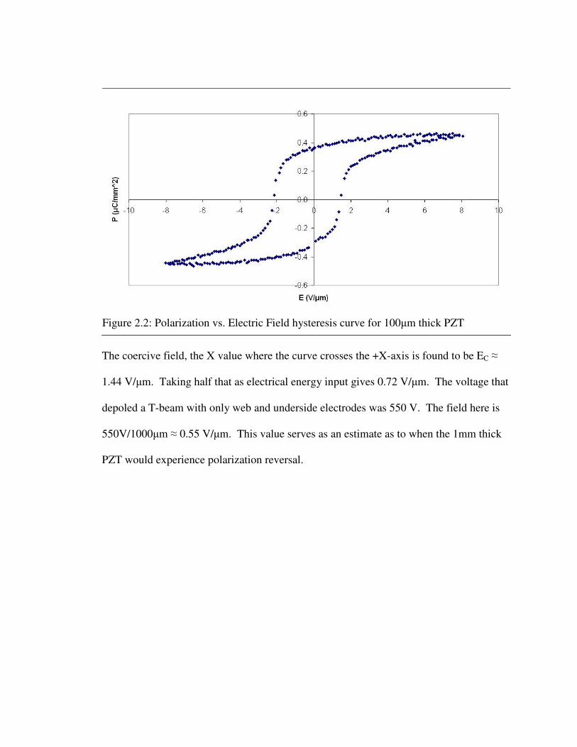
The coercive field, the X value where the curve crosses the +X-axis is found to be EC ≈
1.44 V/µm. Taking half that as electrical energy input gives 0.72 V/µm. The voltage that
depoled a T-beam with only web and underside electrodes was 550 V. The field here is
550V/1000µm ≈ 0.55 V/µm. This value serves as an estimate as to when the 1mm thick
PZT would experience polarization reversal.
Figure 2.2: Polarization vs. Electric Field hysteresis curve for 100µm thick PZT
Appendix C
Comparison with a MEMS Fabrication T-beam
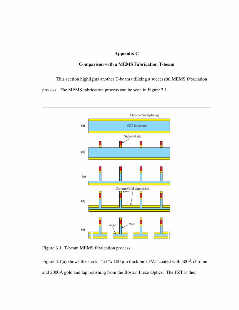
This section highlights another T-beam utilizing a successful MEMS fabrication
process. The MEMS fabrication process can be seen in Figure 3.1.
Figure 3.1(a) shows the stock 1”x1”x 100 µm thick bulk PZT coated with 500Å chrome
and 2000Å gold and lap polishing from the Boston Piezo Optics. The PZT is then
Figure 3.1: T-beam MEMS fabrication process
34
aligned and patterned leaving only the web electroded with chrome/gold. This web
electrode is then electroplated in a nickel solution with 18-22 µm Ni which acts as a hard
mask as shown in Figure 3.1(b). Figure 3.1(c) shows the results of the hour-long ICP-
RIE etch process. A maximum etch rate of 19-25 µm/hr of PZT is obtained using 2000
W of ICP power, 475 W of substrate power, 5 sccm of sulfur hexafluoride (SF6), and 50
sccm of argon (Ar) on the PZT substrate. The T-beams are then released using a dicing
saw. Figure 3.1(c,d) show additional fabrication steps to deposit flange electrodes, which
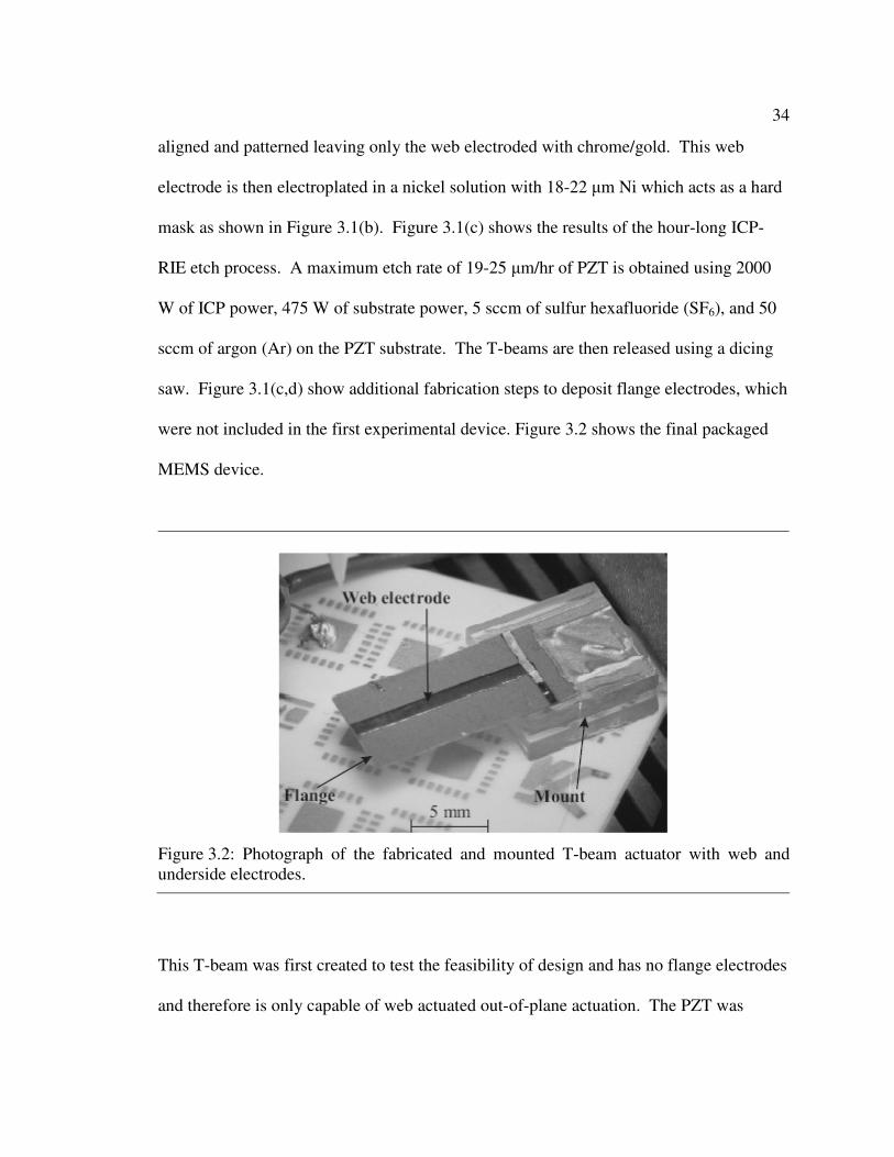
were not included in the first experimental device. Figure 3.2 shows the final packaged
MEMS device.
This T-beam was first created to test the feasibility of design and has no flange electrodes
and therefore is only capable of web actuated out-of-plane actuation. The PZT was
Figure 3.2: Photograph of the fabricated and mounted T-beam actuator with web and underside electrodes.
35
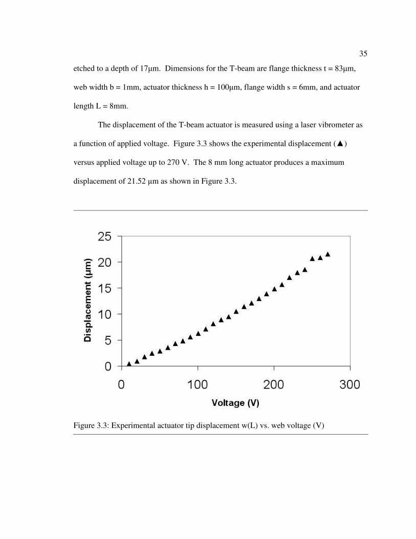
etched to a depth of 17µm. Dimensions for the T-beam are flange thickness t = 83µm,
web width b = 1mm, actuator thickness h = 100µm, flange width s = 6mm, and actuator
length L = 8mm.
The displacement of the T-beam actuator is measured using a laser vibrometer as
a function of applied voltage. Figure 3.3 shows the experimental displacement (▲)
versus applied voltage up to 270 V. The 8 mm long actuator produces a maximum
displacement of 21.52 µm as shown in Figure 3.3.
Figure 3.3: Experimental actuator tip displacement w(L) vs. web voltage (V)
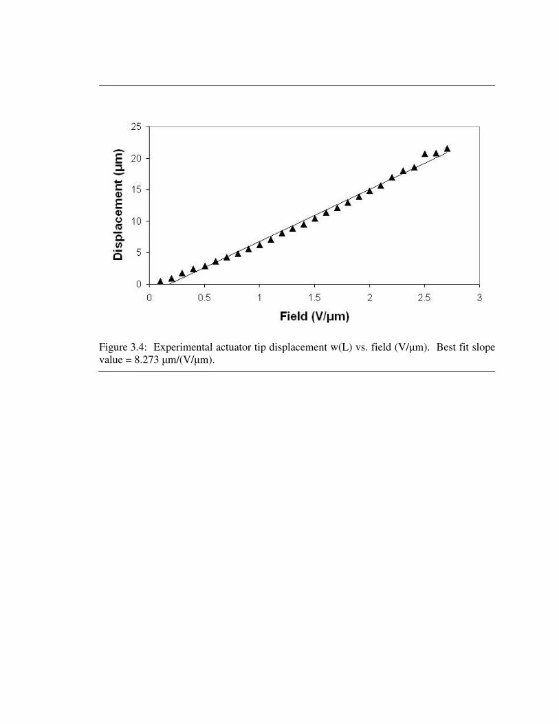
Figure 3.4: Experimental actuator tip displacement w(L) vs. field (V/µm). Best fit slope value = 8.273 µm/(V/µm).
Related Documents


