International Journal of Advances in Engineering & Technology, May 2012. ©IJAET ISSN: 2231-1963 411 Vol. 3, Issue 2, pp. 411-421 DESIGN AND SIMULATION OF MULTILEVEL BASED DSTATCOM P. Surendra Babu 1 and B.V. Sanker Ram 2 1 Department of Electrical and Electronics Engineering, VRS &YRN College of Engineering and Technology, Chirala, A.P, India 2 Department of Electrical and Electronics Engineering, JNTU College of Engineering, Hyderabad, A.P, India ABSTRACT This paper presents an investigation of five-Level Cascaded H – bridge (CHB) Inverter as Distribution Static Compensator (DSTATCOM) in Power System (PS) for compensation of reactive power and harmonics. The advantages of CHB inverter are low harmonic distortion, reduced number of switches and suppression of switching losses. The DSTATCOM helps to improve the power factor and eliminate the Total Harmonics Distortion (THD) drawn from a Non-Liner Diode Rectifier Load (NLDRL). The D-Q reference frame theory is used to generate the reference compensating currents for DSTATCOM while Proportional and Integral (PI) control is used for capacitor dc voltage regulation. A CHB Inverter is considered for shunt compensation of a 11 kV distribution system. Finally a level shifted PWM (LSPWM) and phase shifted PWM (PSPWM) techniques are adopted to investigate the performance of CHB Inverter. The results are obtained through Matlab/Simulink software package. KEYWORDS: DSTATCOM, Level shifted Pulse width modulation (LSPWM), Phase shifted Pulse width modulation (PSPWM), Proportional-Integral (PI) control, CHB multilevel inverter, D-Q reference frame theory. I. INTRODUCTION Modern power systems are of complex networks, where hundreds of generating stations and thousands of load centres are interconnected through long power transmission and distribution networks. Even though the power generation is fairly reliable, the quality of power is not always so reliable. Power distribution system should provide with an uninterrupted flow of energy at smooth sinusoidal voltage at the contracted magnitude level and frequency to their customers. PS especially distribution systems, have numerous non linear loads, which significantly affect the quality of power. Apart from non linear loads, events like capacitor switching, motor starting and unusual faults could also inflict power quality (PQ) problems. PQ problem is defined as any manifested problem in voltage/current or leading to frequency deviations that result in failure or maloperation of customer equipment. Voltage sags and swells are among the many PQ problems the industrial processes have to face. Voltage sags are more severe. During the past few decades, power industries have proved that the adverse impacts on the PQ can be mitigated or avoided by conventional means, and that techniques using fast controlled force commutated power electronics (PE) are even more effective. PQ compensators can be categorized into two main types. One is shunt connected compensation device that effectively eliminates harmonics. The other is the series connected device, which has an edge over the shunt type for correcting the distorted system side voltages and voltage sags caused by power transmission system faults. The STATCOM used in distribution systems is called DSTACOM (Distribution-STACOM) and its configuration is the same, but with small modifications. It can exchange both active and reactive power with the distribution system by varying the amplitude and phase angle of the converter voltage

Welcome message from author
This document is posted to help you gain knowledge. Please leave a comment to let me know what you think about it! Share it to your friends and learn new things together.
Transcript
International Journal of Advances in Engineering & Technology, May 2012.
©IJAET ISSN: 2231-1963
411 Vol. 3, Issue 2, pp. 411-421
DESIGN AND SIMULATION OF MULTILEVEL BASED
DSTATCOM
P. Surendra Babu1 and B.V. Sanker Ram
2
1Department of Electrical and Electronics Engineering, VRS &YRN College of Engineering
and Technology, Chirala, A.P, India 2Department of Electrical and Electronics Engineering, JNTU College of Engineering,
Hyderabad, A.P, India
ABSTRACT
This paper presents an investigation of five-Level Cascaded H – bridge (CHB) Inverter as Distribution Static
Compensator (DSTATCOM) in Power System (PS) for compensation of reactive power and harmonics. The
advantages of CHB inverter are low harmonic distortion, reduced number of switches and suppression of
switching losses. The DSTATCOM helps to improve the power factor and eliminate the Total Harmonics
Distortion (THD) drawn from a Non-Liner Diode Rectifier Load (NLDRL). The D-Q reference frame theory is
used to generate the reference compensating currents for DSTATCOM while Proportional and Integral (PI)
control is used for capacitor dc voltage regulation. A CHB Inverter is considered for shunt compensation of a
11 kV distribution system. Finally a level shifted PWM (LSPWM) and phase shifted PWM (PSPWM) techniques
are adopted to investigate the performance of CHB Inverter. The results are obtained through Matlab/Simulink
software package.
KEYWORDS: DSTATCOM, Level shifted Pulse width modulation (LSPWM), Phase shifted Pulse width
modulation (PSPWM), Proportional-Integral (PI) control, CHB multilevel inverter, D-Q reference frame
theory.
I. INTRODUCTION
Modern power systems are of complex networks, where hundreds of generating stations and
thousands of load centres are interconnected through long power transmission and distribution
networks. Even though the power generation is fairly reliable, the quality of power is not always so
reliable. Power distribution system should provide with an uninterrupted flow of energy at smooth
sinusoidal voltage at the contracted magnitude level and frequency to their customers. PS especially
distribution systems, have numerous non linear loads, which significantly affect the quality of power.
Apart from non linear loads, events like capacitor switching, motor starting and unusual faults could
also inflict power quality (PQ) problems. PQ problem is defined as any manifested problem in
voltage/current or leading to frequency deviations that result in failure or maloperation of customer
equipment. Voltage sags and swells are among the many PQ problems the industrial processes have to
face. Voltage sags are more severe. During the past few decades, power industries have proved that
the adverse impacts on the PQ can be mitigated or avoided by conventional means, and that
techniques using fast controlled force commutated power electronics (PE) are even more effective.
PQ compensators can be categorized into two main types. One is shunt connected compensation
device that effectively eliminates harmonics. The other is the series connected device, which has an
edge over the shunt type for correcting the distorted system side voltages and voltage sags caused by
power transmission system faults.
The STATCOM used in distribution systems is called DSTACOM (Distribution-STACOM) and its
configuration is the same, but with small modifications. It can exchange both active and reactive
power with the distribution system by varying the amplitude and phase angle of the converter voltage
International Journal of Advances in Engineering & Technology, May 2012.
©IJAET ISSN: 2231-1963
412 Vol. 3, Issue 2, pp. 411-421
with respect to the line terminal voltage. A multilevel inverter can reduce the device voltage and the
output harmonics by increasing the number of output voltage levels. There are several types of
multilevel inverters: cascaded H-bridge (CHB), neutral point clamped, flying capacitor [2-5]. In
particular, among these topologies, CHB inverters are being widely used because of their modularity
and simplicity. Various modulation methods can be applied to CHB inverters. CHB inverters can also
increase the number of output voltage levels easily by increasing the number of H-bridges. This paper
presents a DSTATCOM with a proportional integral controller based CHB multilevel inverter for the
harmonics and reactive power mitigation of the nonlinear loads. This type of arrangements have been
widely used for PQ applications due to increase in the number of voltage levels, low switching losses,
low electromagnetic compatibility for hybrid filters and higher order harmonic elimination.
II. DESIGN OF MULTILEVEL BASED DSTATCOM
2.1.PRINCIPLE OF DSTATCOM
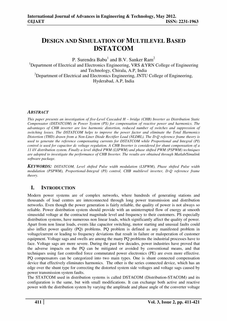
A D-STATCOM (Distribution Static Compensator), which is schematically depicted in Figure-1,
consists of a two-level Voltage Source Converter (VSC), a dc energy storage device, a coupling
transformer connected in shunt to the distribution network through a coupling transformer. The VSC
converts the dc voltage across the storage device into a set of three-phase ac output voltages. These
voltages are in phase and coupled with the ac system through the reactance of the coupling
transformer. Suitable adjustment of the phase and magnitude of the D-STATCOM output voltages
allows effective control of active and reactive power exchanges between the DSTATCOM and the ac
system. Such configuration allows the device to absorb or generate controllable active and reactive
power.
Figure 1 Schematic Diagram of a DSTATCOM
The VSC connected in shunt with the ac system provides a multifunctional topology which can be
used for up to three quite distinct purposes:
1. Voltage regulation and compensation of reactive power;
2. Correction of power factor
3. Elimination of current harmonics.
Here, such device is employed to provide continuous voltage regulation using an indirectly controlled
converter. As shown in Figure-1 the shunt injected current Ish corrects the voltage sag by adjusting the
voltage drop across the system impedance Zth. The value of Ish can be controlled by adjusting the
output voltage of the converter. The shunt injected current Ish can be written as,
Ish = IL – IS = IL – ( Vth – VL ) / Zth (1)
Ish /_η = IL /_- θ (2)
The complex power injection of the D-STATCOM can be expressed as,
Ssh = VL Ish* (3)
It may be mentioned that the effectiveness of the DSTATCOM in correcting voltage sag depends on
the value of Zth or fault level of the load bus. When the shunt injected current Ish is kept in quadrature
with VL, the desired voltage correction can be achieved without injecting any active power into the
system. On the other hand, when the value of Ish is minimized, the same voltage correction can be
achieved with minimum apparent power injection into the system.

International Journal of Advances in Engineering & Technology, May 2012.
©IJAET ISSN: 2231-1963
413 Vol. 3, Issue 2, pp. 411-421
2.2 Control for Reactive Power Compensation
The aim of the control scheme is to maintain constant voltage magnitude at the point where a sensitive
load under system disturbances is connected. The control system only measures the rms voltage at the
load point, i.e., no reactive power measurements are required. The VSC switching strategy is based on
a sinusoidal PWM technique which offers simplicity and good response. Since custom power is a
relatively low-power application, PWM methods offer a more flexible option than the fundamental
frequency switching methods favored in FACTS applications. Apart from this, high switching
frequencies can be used to improve on the efficiency of the converter, without incurring significant
switching losses.
Figure-2 PI control for reactive power compensation
The controller input is an error signal obtained from the reference voltage and the rms terminal
voltage measured. Such error is processed by a PI controller; the output is the angle δ, which is
provided to the PWM signal generator. It is important to note that in this case, of indirectly controlled
converter, there is active and reactive power exchange with the network simultaneously. The PI
controller processes the error signal and generates the required angle to drive the error to zero, i.e. the
load rms voltage is brought back to the reference voltage.
2.3 Control for Harmonics Compensation The Modified Synchronous Frame method is presented in [7]. It is called the instantaneous current component (id-iq) method. This is similar to the Synchronous Reference Frame theory (SRF) method. The transformation angle is now obtained with the voltages of the ac network. The major difference is that, due to voltage harmonics and imbalance, the speed of the reference frame is no longer constant. It varies instantaneously depending of the waveform of the 3-phase voltage system. In this method the compensating currents are obtained from the instantaneous active and reactive current components of the nonlinear load. In the same way, the mains voltages V(a, b, c) and the available currents il (a, b, c) in α-β components must be calculated as given by (4), where C is Clarke Transformation Matrix. However, the load current components are derived from a SRF based on the Park transformation, where ‘θ’ represents the instantaneous voltage vector angle (5). �������� = � ��� �������
(4)
�������� = � ���� ����−���� ����� �������� , � = � �−1 ���� (5)

International Journal of Advances in Engineering & Technology, May 2012.
©IJAET ISSN: 2231-1963
414 Vol. 3, Issue 2, pp. 411-421
FigureFigureFigureFigure----3333 Block diagram of SRF method Fig. 3 shows the block diagram SRF method. Under balanced and sinusoidal voltage conditions angle θ is a uniformly increasing function of time. This transformation angle is sensitive to voltage harmonics and unbalance; therefore dθ/dt may not be constant over a mains period. With transformation given below the direct voltage component is ��� ��!� = "#$%&'$(& � �) �*−�* �) �
(6) ��+)�+*� = "#$%&'$(& ��) −�*�* �) � ��+ �+!�
(7)
��,-./,0�,-./,1�,-./,+ � = �2 ��+)�+*�
(8) 2.4 Cascaded H-Bridge Multilevel Inverter
FigureFigureFigureFigure----4444 Circuit of the single cascaded H-Bridge Inverter Fig.4 shows the circuit model of a single CHB inverter configuration. By using single H-Bridge we
can get 3 voltage levels. The number of output voltage levels of CHB is given by 2n+1 and voltage
step of each level is given by Vdc/2n, where n is number of H-bridges connected in cascaded. The
switching table is given in Table 1. TableTableTableTable----1111 Switching table of single CHB inverter
Switches Turn ON Voltage Level
S1,S2 Vdc
S3,S4 -Vdc
S4,D2 0

International Journal of Advances in Engineering & Technology, May 2012.
©IJAET ISSN: 2231-1963
415 Vol. 3, Issue 2, pp. 411-421
Figure-5 Block diagram of 5-level CHB inverter model
The switching mechanism for 5-level CHB inverter is shown in table-2.
Table 2. Switching table for 5-level CHB Inverter
Switches Turn On Voltage Level
S1, S2 Vdc
S1,S2,S5,S6 2Vdc
S4,D2,S8,D6 0
S3,S4 -Vdc
S3,S4,S7,S8 -2Vdc
III. DESIGN OF SINGLE H-BRIDGE CELL
3.1. Device Current
The IGBT and DIODE currents can be obtained from the load current by multiplying with the
corresponding duty cycles. Duty cycle, d = ½(1+Kmsinωt), Where, m = modulation index K = +1 for
IGBT, -1 for Diode. For a load current given by
Iph = √2 I sin (wt – ф) (9)
Then the device current can be written as follows. ∴ � 456+4 = √88 � sin<=� − ∅?@ <1 + BC sin =�? (10)
The average value of the device current over a cycle is calculated as
�05D = 12F G √22 � sin<=� − ∅?@ <1 + BC sin =�? �=�H'II
=√2� � "8H + J .D cos M� (11)
The device RMS current can be written as
�N.O = P G 12F <√2� sin< =� − ∅??8 @ 12 @ <<1 + BC sin =�? �=�?H'II
International Journal of Advances in Engineering & Technology, May 2012.
©IJAET
416
= √2� #"D + J.QH cos M
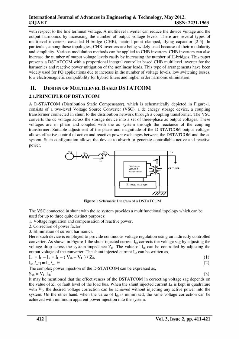
3.2 IGBT Loss Calculation:
IGBT loss can be calculated by the sum of switchin
can be calculated by,
Pon (IGBT) = Vceo * Iavg (igbt) + I2
rms (igbt)�05D <6D1R? = √2� � "8H + .D ���M�N.O <6D1R? = √2�#�"D + .QH ���MValues of Vceo and rceo at any junction temperature can be obtained from the
vs. Vce) of the IGBT as shown in Fig .6.
The switching losses are the sum of all turn
Esw = Eon + Eoff = a + bI + cIAssuming the linear dependence, switching energy
Esw = (a + bI + cI2) *
$ST$UVWHere VDC is the actual DC-Link voltage and V
Switching losses are calculated by summing up the switching energiesXOY = "2Z Σ\]OY<�?
Here ‘n’ depends on the switching frequency
Psw = "2Z Σ\< + �� + ��8? =
After considering the DC-Link voltage variations, switching losses of the IGBT can be written as
follows.
Psw (IGBT) = fsw �08 + 1H + +^&_ � ∗So, the sum of conduction and switching losses is the total losses given by
PT (IGBT) = Pon (IGBT) + Psw (IGBT)
3.3 Diode Loss Calculation:
The DIODE switching losses consist of its reverse recovery losses; the turn
negligible.
Erec = a + bI + cI2
Psw (DIODE) = fsw �08 + 1H + +^&_ � ∗So, the sum of conduction and switching losses gives the total DIODE looses
PT (DIODE) = Pon (DIODE) + Psw (DIODE)
International Journal of Advances in Engineering & Technology, May 2012.
Vol. 3, Issue 2, pp.
3.2 IGBT Loss Calculation:
IGBT loss can be calculated by the sum of switching loss and conduction loss. The conduction loss
rms (igbt) * rceo ���M�
���M�
at any junction temperature can be obtained from the output characteristics (Ic
vs. Vce) of the IGBT as shown in Fig .6.
Figure 6 IGBT output characteristics
The switching losses are the sum of all turn-on and turn-off energies at the switching events
= a + bI + cI2
Assuming the linear dependence, switching energy STUVW
Link voltage and Vnom is the DC-Link Voltage at which E
Switching losses are calculated by summing up the switching energies.
Here ‘n’ depends on the switching frequency. ? = "2Z �08 + 1H + +^&_ �
Link voltage variations, switching losses of the IGBT can be written as
� ∗ $ST$UVa
So, the sum of conduction and switching losses is the total losses given by
sw (IGBT)
3.3 Diode Loss Calculation:
The DIODE switching losses consist of its reverse recovery losses; the turn
� ∗ $ST$UVa
So, the sum of conduction and switching losses gives the total DIODE looses.
sw (DIODE)
International Journal of Advances in Engineering & Technology, May 2012.
ISSN: 2231-1963
Vol. 3, Issue 2, pp. 411-421
(12)
g loss and conduction loss. The conduction loss
(13)
(14)
(15)
output characteristics (Ic
off energies at the switching events
(16)
(17)
Link Voltage at which Esw is given.
(18)
(19)
Link voltage variations, switching losses of the IGBT can be written as
(20)
(21)
The DIODE switching losses consist of its reverse recovery losses; the turn-on losses are
(22)
(23)
(24)
International Journal of Advances in Engineering & Technology, May 2012.
©IJAET
417
The total loss per one switch (IGBT+DIODE) is the sum of one IGBT and DIODE loss.
PT = PT (IGBT) + Psw (DIODE)
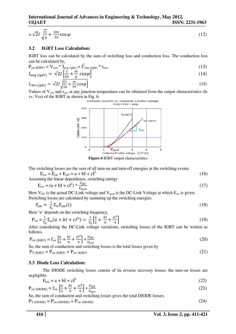
3.4 Thermal Calculations
The junction temperatures of the IGBT and DIODE are calculated based on the device power losses
and thermal resistances. The thermal resistance equivalent circuit for a module is shown in Fig
this design the thermal calculations are started with heat sink temperature as the reference
temperature. So, the case temperature from the model can be written as follows.
Tc = PT Rth (c-h) + Th
Here Rth(c-h) = Thermal resistance between case and heat sink
PT = Total Power Loss (IGBT + DIODE)
IGBT junction temperature is the sum of the case temperature and temperature raise due
losses in the IGBT.
Tj (IGBT) = PT (IGBT) Rth (j
The DIODE junction temperature is the sum of the case temperature and temperature raise due to the
power losses in the DIODE.
Tj (DIODE) = PT (DIODE) Rth (j-c) DIODE + T
The above calculations are done based on the average power losses computed over a cycle. So, the
corresponding thermal calculation gives the
calculated values close to the actual values, transient temperature values are to be added to the
average junction temperatures.
Figure 7
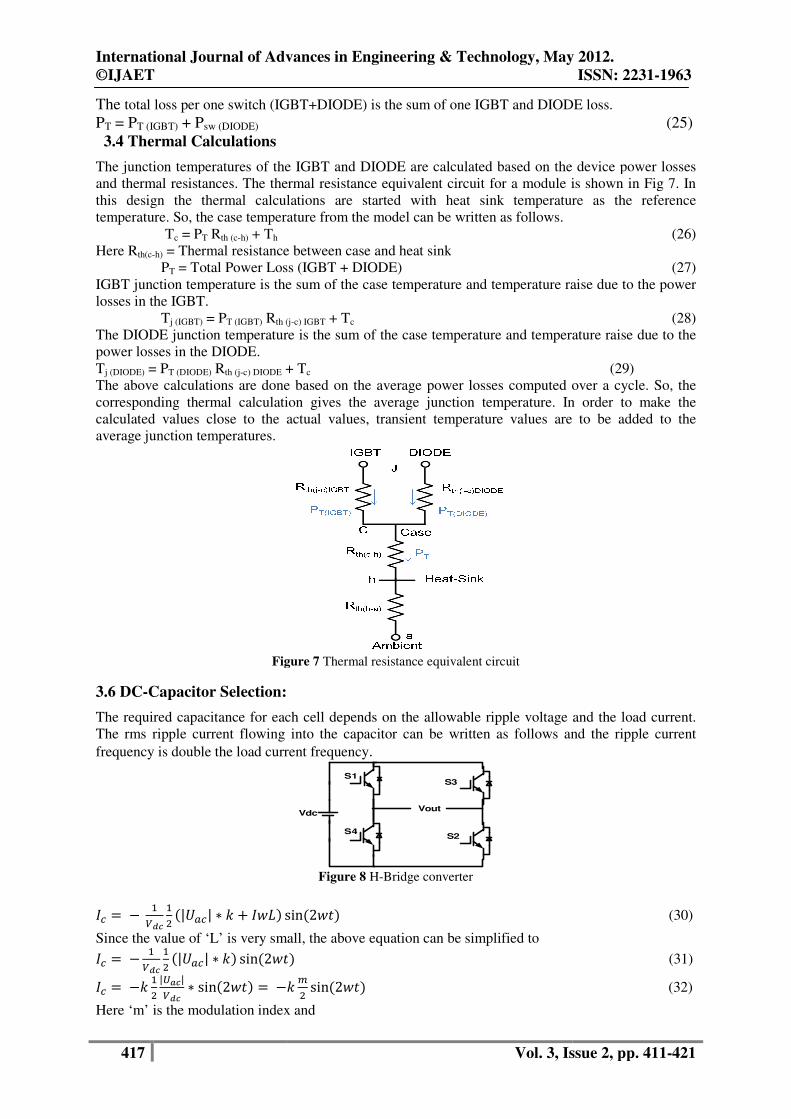
3.6 DC-Capacitor Selection:
The required capacitance for each cell depends on the allowable ripple voltage and the load current.
The rms ripple current flowing into the capacitor can be written as follows and the ripple current
frequency is double the load current frequency
�+ = − "$bc "8 <|e0+| ∗ B + �=f? sinSince the value of ‘L’ is very small, the above equation can be simplified to�+ = − "$bc "8 <|e0+| ∗ B? sin<2=��+ = −B "8 |ghc|$bc ∗ sin<2=�? = −Here ‘m’ is the modulation index and
International Journal of Advances in Engineering & Technology, May 2012.
Vol. 3, Issue 2, pp.
total loss per one switch (IGBT+DIODE) is the sum of one IGBT and DIODE loss.
The junction temperatures of the IGBT and DIODE are calculated based on the device power losses
and thermal resistances. The thermal resistance equivalent circuit for a module is shown in Fig
this design the thermal calculations are started with heat sink temperature as the reference
temperature. So, the case temperature from the model can be written as follows.
= Thermal resistance between case and heat sink
= Total Power Loss (IGBT + DIODE)
IGBT junction temperature is the sum of the case temperature and temperature raise due
th (j-c) IGBT + Tc
The DIODE junction temperature is the sum of the case temperature and temperature raise due to the
+ Tc
The above calculations are done based on the average power losses computed over a cycle. So, the
corresponding thermal calculation gives the average junction temperature. In order to make the
calculated values close to the actual values, transient temperature values are to be added to the
Figure 7 Thermal resistance equivalent circuit
Capacitor Selection:
The required capacitance for each cell depends on the allowable ripple voltage and the load current.
The rms ripple current flowing into the capacitor can be written as follows and the ripple current
frequency is double the load current frequency.
Vout
S3
S2S4
S1
Vdc
Figure 8 H-Bridge converter
? sin<2=�?
Since the value of ‘L’ is very small, the above equation can be simplified to =�? −B .8 sin<2=�?
modulation index and
International Journal of Advances in Engineering & Technology, May 2012.
ISSN: 2231-1963
Vol. 3, Issue 2, pp. 411-421
total loss per one switch (IGBT+DIODE) is the sum of one IGBT and DIODE loss.
(25)
The junction temperatures of the IGBT and DIODE are calculated based on the device power losses
and thermal resistances. The thermal resistance equivalent circuit for a module is shown in Fig 7. In
this design the thermal calculations are started with heat sink temperature as the reference
(26)
(27)
IGBT junction temperature is the sum of the case temperature and temperature raise due to the power
(28)
The DIODE junction temperature is the sum of the case temperature and temperature raise due to the
(29)
The above calculations are done based on the average power losses computed over a cycle. So, the
average junction temperature. In order to make the
calculated values close to the actual values, transient temperature values are to be added to the
The required capacitance for each cell depends on the allowable ripple voltage and the load current.
The rms ripple current flowing into the capacitor can be written as follows and the ripple current
(30)
(31)
(32)

International Journal of Advances in Engineering & Technology, May 2012.
©IJAET ISSN: 2231-1963
418 Vol. 3, Issue 2, pp. 411-421
�+/ = ijj R ; .8 �√2= C2w*∆V Vdc
C = ._Y "∆$∗$bc √2� (33)
3.7 PWM Techniques for CHB Inverter The most popular PWM techniques for CHB inverter are 1. Phase Shifted Carrier PWM (PSCPWM), 2. Level Shifted Carrier PWM (LSCPWM). 3.7.1. Phase Shifted Carrier PWM (PSCPWM)3.7.1. Phase Shifted Carrier PWM (PSCPWM)3.7.1. Phase Shifted Carrier PWM (PSCPWM)3.7.1. Phase Shifted Carrier PWM (PSCPWM)
FigFigFigFigureureureure 9999 phase shifted carrier PWM Fig 9 shows the Phase shifted carrier pulse width modulation. Each cell is modulated independently using sinusoidal unipolar pulse width modulation and bipolar pulse width modulation respectively, providing an even power distribution among the cells. A carrier phase shift of 180°/m (No. of levels) for cascaded inverter is introduced across the cells to generate the stepped multilevel output waveform with lower distortion. 3.7.2. Level Shifted Carrier PWM (LSCPWM):3.7.2. Level Shifted Carrier PWM (LSCPWM):3.7.2. Level Shifted Carrier PWM (LSCPWM):3.7.2. Level Shifted Carrier PWM (LSCPWM):
FigFigFigFigureureureure 10101010 Level shifted carrier PWM Fig 10 shows the Level shifted carrier pulse width modulation. Each cell is modulated independently
using sinusoidal unipolar pulse width modulation and bipolar pulse width modulation respectively,
providing an even power distribution among the cells. A carrier Level shift by 1/m (No. of levels) for
cascaded inverter is introduced across the cells to generate the stepped multilevel output waveform
with lower distortion.
IV. MATLAB/SIMULINK MODELING AND SIMULATION RESULTS
International Journal of Advances in Engineering & Technology, May 2012.
©IJAET ISSN: 2231-1963
419 Vol. 3, Issue 2, pp. 411-421
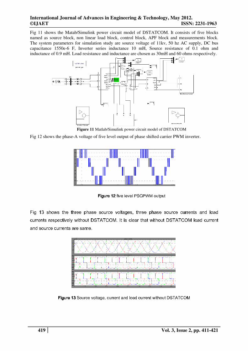
Fig 11 shows the Matab/Simulink power circuit model of DSTATCOM. It consists of five blocks
named as source block, non linear load block, control block, APF block and measurements block.
The system parameters for simulation study are source voltage of 11kv, 50 hz AC supply, DC bus
capacitance 1550e-6 F, Inverter series inductance 10 mH, Source resistance of 0.1 ohm and
inductance of 0.9 mH. Load resistance and inductance are chosen as 30mH and 60 ohms respectively.
Figure 11 Matlab/Simulink power circuit model of DSTATCOM
Fig 12 shows the phase-A voltage of five level output of phase shifted carrier PWM inverter.
FigFigFigFigureureureure 12121212 five level PSCPWM output Fig 13 shows the three phase source voltages, three phase source currents and load currents respectively without DSTATCOM. It is clear that without DSTATCOM load current and source currents are same.
FigFigFigFigureureureure 13131313 Source voltage, current and load current without DSTATCOM
International Journal of Advances in Engineering & Technology, May 2012.
©IJAET ISSN: 2231-1963
420 Vol. 3, Issue 2, pp. 411-421
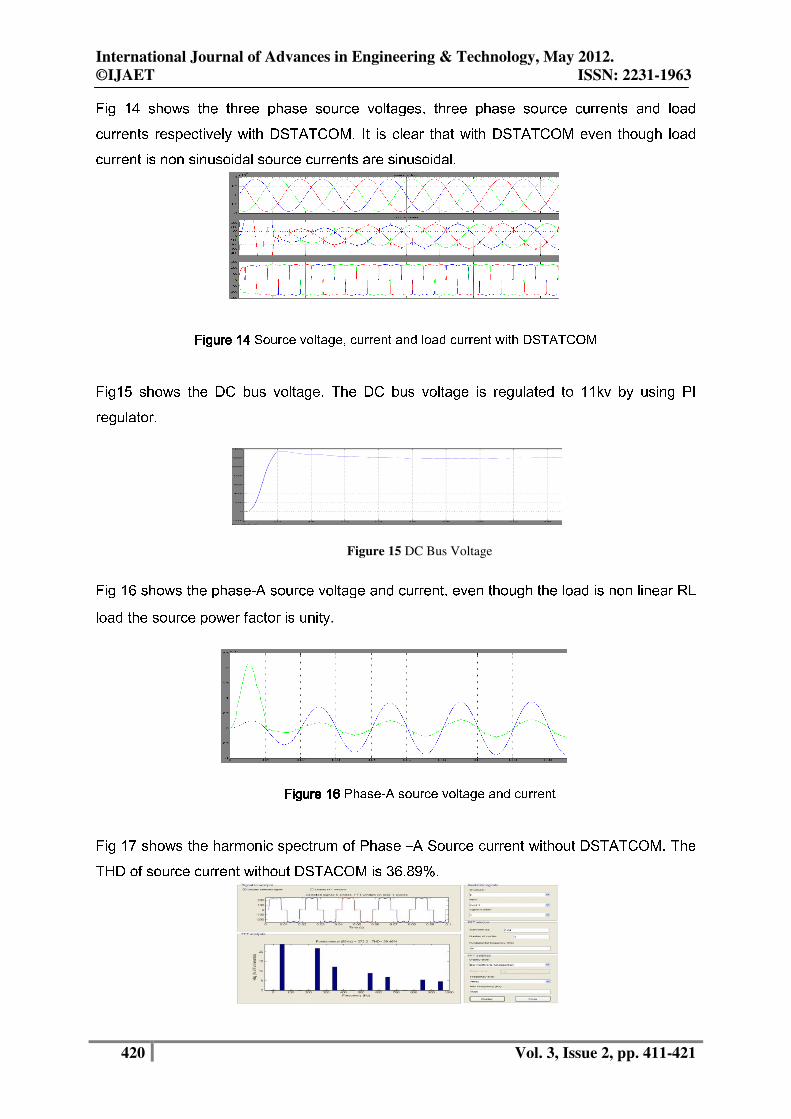
Fig 14 shows the three phase source voltages, three phase source currents and load currents respectively with DSTATCOM. It is clear that with DSTATCOM even though load current is non sinusoidal source currents are sinusoidal.
FigFigFigFigureureureure 14141414 Source voltage, current and load current with DSTATCOM Fig15 shows the DC bus voltage. The DC bus voltage is regulated to 11kv by using PI regulator.
Figure 15 DC Bus Voltage
Fig 16 shows the phase-A source voltage and current, even though the load is non linear RL load the source power factor is unity.
FigFigFigFigureureureure 16161616 Phase-A source voltage and current
Fig 17 shows the harmonic spectrum of Phase –A Source current without DSTATCOM. The THD of source current without DSTACOM is 36.89%.

International Journal of Advances in Engineering & Technology, May 2012.
©IJAET ISSN: 2231-1963
421 Vol. 3, Issue 2, pp. 411-421
Figure 17 Harmonic spectrum of Phase-A Source current without DSTATCOM
Fig 18 shows the harmonic spectrum of Phase –A Source current with DSTATCOM. The THD of source current without DSTACOM is 5.05%
Figure 18 Harmonic spectrum of Phase-A Source current with DSTATCOM
V. CONCLUSION
A DSTATCOM with five level CHB inverter is investigated. Mathematical model for single H-Bridge
inverter is developed which can be extended to multi H-Bridge. The source voltage , load voltage,
source current, load current, power factor simulation results under non-linear loads are presented.
Finally Matlab/Simulink based model is developed and simulation results are presented.
REFERENCES
[1] K.A Corzine, and Y.L Familiant, “A New Cascaded Multi-level H-Bridge Drive,” IEEE Trans.
Power.Electron., vol.17, no.1, pp.125-131. Jan 2002.
[2] J.S.Lai, and F.Z.Peng “Multilevel converters – A new bread of converters, ”IEEE Trans. Ind.Appli., vol.32,
no.3, pp.509-517. May/ Jun. 1996.
[3] T.A.Maynard, M.Fadel and N.Aouda, “Modelling of multilevel converter,” IEEE Trans. Ind.Electron.,
vol.44, pp.356-364. Jun.1997.
[4] P.Bhagwat, and V.R.Stefanovic, “Generalized structure of a multilevel PWM Inverter,” IEEE Trans. Ind.
Appln, Vol.1A-19, no.6, pp.1057-1069,
Nov./Dec..1983.
[5] J.Rodriguez, Jih-sheng Lai, and F Zheng peng, “Multilevel Inverters; A Survey of Topologies, Controls, and
Applications,” IEEE Trans. Ind. Electron., vol.49 , no4., pp.724-738. Aug.2002.
[6] Roozbeh Naderi, and Abdolreza rahmati, “Phase-shifted carrier PWM technique for general cascaded
inverters,” IEEE Trans. Power.Electron., vol.23, no.3, pp.1257-1269. May.2008.
Author:
P. Surendra Babu is currently working as Associate Professor & HOD, EEE in VRS &
YRN College of Engineering And Technology CHIRALA. He completed his B.tech in the
year 2002 at JNTU Anantapur. He completed his M.tech in the year 2007at JNTU
Hyderabad. He has over 10 years of teaching experience in various positions. His research
areas include Fact Devices ,Power Systems.
Related Documents


![Enhancement of Power Quality by Optimal Placement of ...harmonics, unbalance and voltage sag using DVR has been suggested in [12]. Placement of DSTATCOM for mitigation of voltage sag](https://static.cupdf.com/doc/110x72/5ed3304bf7f9301169375c90/enhancement-of-power-quality-by-optimal-placement-of-harmonics-unbalance-and.jpg)