Design and optimization of Schottky diodes in CMOS technology with application to passive RFID systems Auto-ID lab Adelaide

Design and optimization of Schottky diodes in CMOS technology with application to passive RFID systems Auto-ID lab Adelaide.
Dec 28, 2015
Welcome message from author
This document is posted to help you gain knowledge. Please leave a comment to let me know what you think about it! Share it to your friends and learn new things together.
Transcript

Design and optimization of Schottky diodes in CMOS
technology with application to passive RFID systems
Auto-ID lab Adelaide

Overview
• Introduction.• Design and layout of Schottky diode.• Modelling of designed SBD.• Applications.• Fabrication and measurements.• Conclusion.
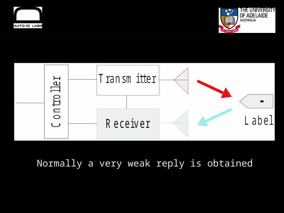
The General RFID Idea
Normally a very weak reply is obtained
The black spot
Example Applications
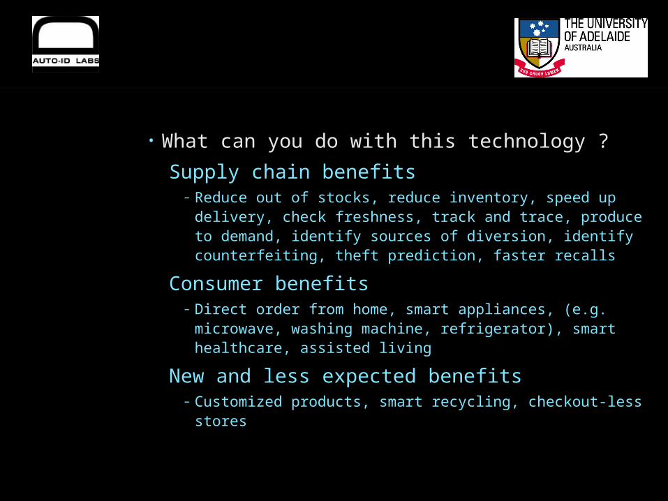
• What can you do with this technology ?
Supply chain benefits– Reduce out of stocks, reduce inventory, speed up
delivery, check freshness, track and trace, produce to demand, identify sources of diversion, identify counterfeiting, theft prediction, faster recalls
Consumer benefits– Direct order from home, smart appliances, (e.g.
microwave, washing machine, refrigerator), smart healthcare, assisted living
New and less expected benefits– Customized products, smart recycling, checkout-less
stores
Passive RFID
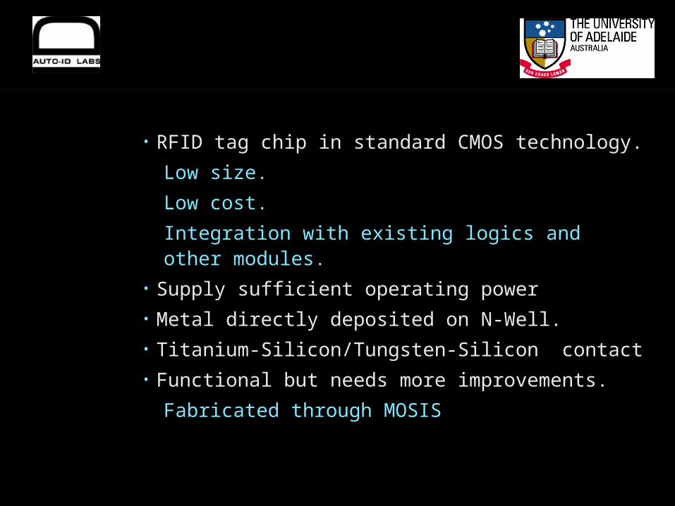
• RFID tag chip in standard CMOS technology.
Low size.
Low cost.
Integration with existing logics and other modules.
• Supply sufficient operating power• Metal directly deposited on N-Well.• Titanium-Silicon/Tungsten-Silicon contact• Functional but needs more improvements.
Fabricated through MOSIS

Cross Sectional view of SBD
• Design a diode structure to minimize series resistance of n-well.
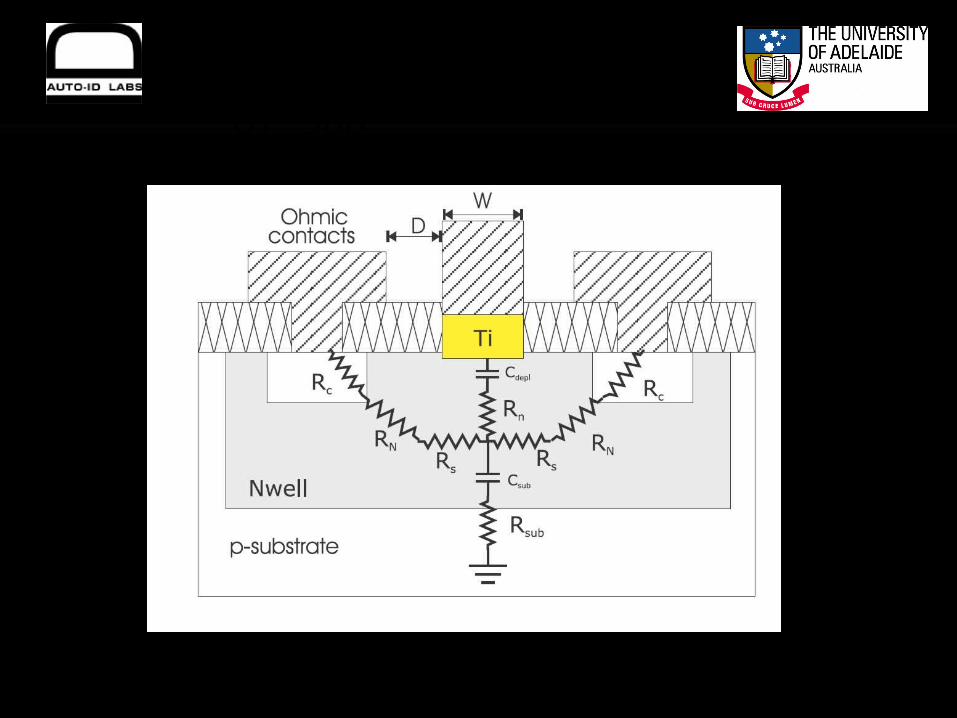
Cross Sectional view of SBD
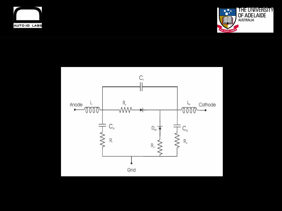
Equivalent circuit

Multi-finger Schottky contact
• Reducing the series resistanceIncreasing the perimeter
Decrease junction capacitance
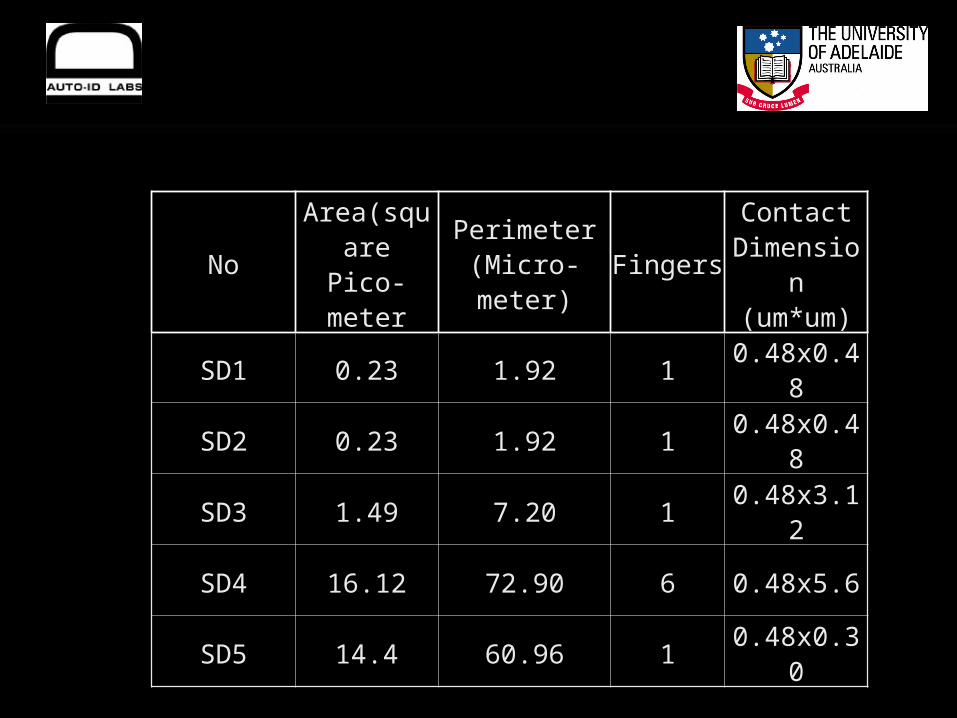
Prototyped SBD sizes
NoArea(squa
re Pico-meter
Perimeter (Micro-meter)
FingersContact
Dimension (um*um)
SD1 0.23 1.92 1 0.48x0.48
SD2 0.23 1.92 1 0.48x0.48
SD3 1.49 7.20 1 0.48x3.12
SD4 16.12 72.90 6 0.48x5.6
SD5 14.4 60.96 1 0.48x0.30
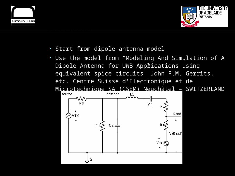
RFID Ant Model & Matching
• Start from dipole antenna model• Use the model from “Modeling And Simulation of A Dipole
Antenna for UWB Applications using equivalent spice circuits” John F.M. Gerrits, etc. Centre Suisse d'Electronique et de Microtechnique SA (CSEM) Neuchâtel – SWITZERLAND
+VTX-
Rs
R1 C2
C1 Rl
Rr
L1
+Vrx-
Rrad
+
V(Rrad)
-
0
source antenna

Matching and Optimal Input Level
• Equivalent circuit of RFID chip
• Vrx value for 73 (half wavelength dipole) radiation resistance at 150uW input
• 50 resistor voltage swing
Rs jXs
VuWRPV rpprx 296.0731502222)(
VuW
RR
RRPV
rload
loadrppload
120.05073
507315022
22)(

Matching and Optimal Input Level (Cont.)
• Quality factor of the RFID circuit (Serial configuration)
• Maximum voltage swing across the RFID chip• 150uW input would have a 0.7V Vp-p input
No other rectifier structure will work except Schottky diode rectifier structure
• Hard to decrease the input capacitance to increase the Q
Rs
XsQ
QRR
RRPV
sr
srpp
22

Rectifier circuit (SBD application)

SBD Rectifier layout
Measurement Plan
• Discrete SBD testGSD probing pads for de-embeddingS parametersDC parameters
• SBD rectifier testInput impedanceMatching circuit/boardAntennaReader/Signal generator and
PA+Antenna; Optimised tag

Discrete SBD Test

Prototype Reader

Future Work
• Test and extract the model parameters• Validating the SBD model• Improve the quality factor of the SBD• Increase reverse direction breakdown
voltage by guard ring (fabricated version dose not have)
• Improve efficiency by reducing parasitic capacitance
• Better impedance matching capabilities

Q&A
• Thank You
Related Documents