Design and optical characterization of photonic crystal lasers with organic gain material This article has been downloaded from IOPscience. Please scroll down to see the full text article. 2010 J. Opt. 12 065003 (http://iopscience.iop.org/2040-8986/12/6/065003) Download details: IP Address: 195.176.20.45 The article was downloaded on 19/08/2010 at 13:37 Please note that terms and conditions apply. View the table of contents for this issue, or go to the journal homepage for more Home Search Collections Journals About Contact us My IOPscience

Welcome message from author
This document is posted to help you gain knowledge. Please leave a comment to let me know what you think about it! Share it to your friends and learn new things together.
Transcript

Design and optical characterization of photonic crystal lasers with organic gain material
This article has been downloaded from IOPscience. Please scroll down to see the full text article.
2010 J. Opt. 12 065003
(http://iopscience.iop.org/2040-8986/12/6/065003)
Download details:
IP Address: 195.176.20.45
The article was downloaded on 19/08/2010 at 13:37
Please note that terms and conditions apply.
View the table of contents for this issue, or go to the journal homepage for more
Home Search Collections Journals About Contact us My IOPscience

IOP PUBLISHING JOURNAL OF OPTICS
J. Opt. 12 (2010) 065003 (8pp) doi:10.1088/2040-8978/12/6/065003
Design and optical characterization ofphotonic crystal lasers with organic gainmaterialK Baumann1,4, T Stoferle1, N Moll1, G Raino1, R F Mahrt1,5,T Wahlbrink2, J Bolten2 and U Scherf3
1 IBM Research–Zurich, Saumerstrasse 4, 8803 Ruschlikon, Switzerland2 Advanced Microelectronic Center Aachen, AMO GmbH, Otto-Blumenthal Strasse 25,52074, Germany3 Makromolekulare Chemie, Fachbereich C-Mathematik und Naturwissenschaften,Bergische Universitat Wuppertal, Gauss-Strasse 20, 42119 Wuppertal, Germany
E-mail: [email protected]
Received 18 February 2010, accepted for publication 5 May 2010Published 10 June 2010Online at stacks.iop.org/JOpt/12/065003
AbstractWe present a design concept for an optimized surface-emitting laser with two-dimensionalfeedback structure and organic gain material. The basic laser structure consists of an array ofholes within a thin film of Ta2O5. The optical properties of such feedback structures areinvestigated theoretically and experimentally. Combining first-order with second-order photonicstructures leads to a higher quality factor of the feedback structure, resulting in a lower laserthreshold and/or a much smaller footprint of the laser.
Keywords: photonic-crystal laser, organic gain material
(Some figures in this article are in colour only in the electronic version)
1. Introduction
Novel and innovative hardware concepts and devices arerequired because today’s electrical technologies will soon befacing physical limits and the demand for high bandwidth fordata transmission is still rapidly increasing. However, reachingthis performance ceiling could be postponed significantly byapplying optical interconnects on short distances, such as oncard-to-card, on-card, and ultimately on-chip scales. To meetthese new challenges, novel laser devices are of the utmostimportance. Such devices should offer a low lasing threshold,a small-footprint, a significant decrease of processing costs,improved packaging opportunities, great flexibility for possiblegain materials, and CMOS back-end-of-the-line compatibility.Organic gain materials are ideal candidates for realizing suchnovel photonic devices [1–4].
In recent years, organic semiconductor materials haveattracted increasing interest owing to their excellent optical
4 Present address: Institute for Quantum Electronics, ETH Zurich,Schafmattstrasse 16, 8093 Zurich, Switzerland.5 Author to whom any correspondence should be addressed.
properties and their great potential for display, sensing, andsolar-cell applications. Furthermore, these materials exhibitlow lasing thresholds and a spectrally broad gain, enablingthe emission wavelength to be tuned across the entire visiblespectrum [1–7]. Methyl-substituted ladder-type poly-para-phenylene (MeLPPP) has been proven to be among thematerials with the highest optical gain, about 2000 cm−1 [8].
Typical resonator designs for organic lasers reportedso far consist of linear and circular distributed feedback(DFB) [8–10] as well as microring [11] and microcavity [2, 12]structures, enabling optical pumping. The feedback in DFBstructures relies on the index contrast (�n) between the gainmaterial and the glass substrate [13–16]. Typical �n valuesrange from 0.2 to 0.3. Increasing the index contrast wouldincrease the effect of the periodic structures and consequentlythe optical feedback. Therefore, we have designed andfabricated a vertical surface-emitting organic laser structurebased on a layer of high-index tantalum pentoxide (Ta2O5) thatexhibits a reduced lasing threshold. The feedback structureconsists of a square lattice of holes etched into the Ta2O5 layer.By doing so we increased the index contrast by employing a
2040-8978/10/065003+08$30.00 © 2010 IOP Publishing Ltd Printed in the UK & the USA1

J. Opt. 12 (2010) 065003 K Baumann et al
thin high-index film as the photonic crystal layer. Additionally,we enclose a second-diffraction-order vertically emitting laserlattice by mirrors to reflect light that otherwise is lost due toleakage back into the active region. Therefore, more light isconfined within the second-order feedback region, resultingin a considerably reduced lasing threshold. This allows theconstruction of much smaller devices exhibiting ultra-smallfootprints. The mirrors are designed as first-diffraction-orderphotonic structures exhibiting a bandgap centered at the lasingwavelength. Note that these structures exhibit no vertical out-coupling. As the mirrors are integrated into the same planarTa2O5 layer as the second-order lasing structure the only freedesign parameters left are the lattice constant and the radii ofthe holes forming the structure.
The paper is organized as follows: in section 2,we briefly describe the simulation methods followed bythe work specification in order to achieve an optimizedsecond-order feedback structure starting from a square latticeof holes. Subsequently, laser threshold characteristicsfor structures with different feedback length have beeninvestigated experimentally. In section 3 we describe in detailthe novel mixed-order design. Here, by means of modelingwe focus on the optimization of the structure by varyingthe number of first- and second-order periods as well as thedistance between them. The numerical results were verifiedby optical experiments carried out on samples fabricatedaccording to the optimized design. Finally, in section 4 wesummarize our results and finish with a conclusion.
2. Simulation and design of second-order laserstructures
2.1. Simulation methods
Photonic band structures can be employed in a similar wayto electronic band structures in solid-state physics, namely,to present the behavior of photons in a periodic structure,a so-called photonic crystal. To calculate the photonicband structures, we used the MIT Photonic Bands (MPB)program, which computes the fully vectorial eigenmodes ofMaxwell’s equations with periodic boundary conditions bypreconditioned conjugate-gradient minimization of the blockRayleigh quotient in a plane-wave basis [17].
Three-dimensional (3D) calculations performed usingMPB yield accurate eigenmodes of the electromagnetic fieldwithin the full 3D structure. Monitoring the energy of themode in the waveguide provides a criterion to distinguishbetween the desired eigenmodes and vacuum modes. In3D calculations, true transverse-electric (TE) and transverse-magnetic (TM) modes do not exist, which poses an additionalissue. The modes can, however, show even or odd symmetrywith respect to the lateral symmetry plane of the 3D structure.If the structure has no lateral symmetry plane, for instance ifthe upper cladding is a different material from the substrate,even-like and odd-like modes, meaning that a mode hasa predominantly even or odd symmetry, can exist [14].In addition, 2D calculations are performed using MPB,which yield the eigenmodes of a periodic structure that has
features only in the XY plane. The main advantage of 2Dcalculations is that, compared with 3D calculations, they arevery fast. However, the limitation to the XY plane demandsan approximate effective dielectric constant of the photonicstructure in the vertical (Z -) direction, resulting in a qualitativedescription of the eigenmodes.
To obtain the temporal behavior of the photonic structure,a finite difference time domain (FDTD) algorithm [18], namelyMEEP [19], is used. The FDTD algorithm discretizesMaxwell’s equations and evaluates them on a spatial grid ofpoints. Therefore the actual propagation of the electromagneticwave in the structure is modeled. The geometry with dielectricconstants has to be specified and forms the computationaldomain. In contrast to MPB, which only supports periodicboundary conditions, MEEP accepts other boundary types, forexample, the absorbing boundary conditions important for auseful characterization of a real device.
2.2. Design of second-order laser structures
In recent publications, Harbers et al [14–16] reported on avertical surface-emitting organic laser structure with a high-index TiO2 2D photonic crystal layer that exhibits a lowerlasing threshold than an otherwise similar structure withoutthe high-index layer. However, because of the difficultmanufacturing process for amorphous TiO2 of high opticalquality, we used Ta2O5 as an alternative material in thiswork. It exhibits negligible absorbance in the visible andnear-infrared spectral range [20], shows low scattering losses,and is compatible with CMOS technology. The completematerial stack consists of Si, SiO2, structured Ta2O5 andMeLPPP as the gain material. The first design is based ona second-order feedback structure in which light is coupledout perpendicularly to the photonic crystal plane. We choosea square lattice of circular holes to account for a low-endmanufacturing process. Silicon is transparent for wavelengthsbeyond λ = 1.2 μm, whereas the gain material (MeLPPP)emits at λ ≈ 500 nm, ruling out silicon as the substrate.Instead, SiO2 with its low refractive index (n ≈ 1.45) and itsnegligible absorption in the visible range is used. Therefore,a 1.8 μm-thick layer of SiO2 is thermally grown on top of thesilicon wafer to prevent leakage into the silicon substrate.
Beyond this basic configuration, four geometry parame-ters can be adjusted, as can be inferred from figure 1, wherea vertical and a lateral cross sections of the structure aredisplayed. The parameters are the thickness of the Ta2O5 layer,h, the radius of the holes in the Ta2O5 layer, r , the thicknessof the MeLPPP layer, H (note that this thickness also includesthe Ta2O5 layer because the gain material penetrates into theholes of the Ta2O5 layer), and the lattice constant, a. In thispaper, the dimensions (a), frequencies (c/a) and wavevectors(2π/a) are given in units of the lattice constant a because of thescale invariance of Maxwell’s equations. The basic parameterset (H = 0.7a, h = 0.1a and r = 0.35a) stems from a recentpublication [14] and was chosen as starting point. A full 3Dband structure for this parameter set calculated in the frequencydomain is shown in figure 2. The points �, X and M are pointsof high symmetry in the irreducible Brillouin zone. Because
2

J. Opt. 12 (2010) 065003 K Baumann et al
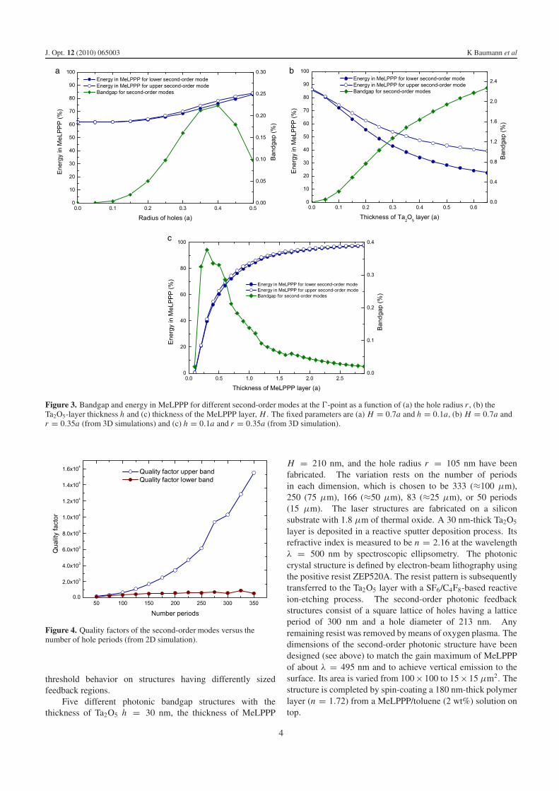
Figure 1. (a) Vertical cross section of the photonic crystal unit cell, showing the design parameters H, h, r and a. (b) Lateral cross section ofthe photonic crystal.
the size of the bandgap is proportional to the coupling of thetwo counter-propagating modes, a larger bandgap gives rise toa stronger coupling which reduces the device size and/or thelasing threshold. Another important quantity is the fraction offield energy confined within the MeLPPP gain layer, becauseonly this part of the field can be amplified. Therefore, thebandgap and the energy confined in the MeLPPP are the twobasic criteria determining the final geometry of the devicestructure. However, there is no simultaneous optimum for thesetwo basic parameters for the same device geometry. Hence, theinfluence of each parameter on the bandgap and the energy inMeLPPP will be discussed. Figure 3(a) shows the bandgap andenergy in MeLPPP for the second-order modes at the �-pointas a function of the hole radius in Ta2O5. Here, the thicknessof the Ta2O5 layer, h, and the thickness of the MeLPPP layer,H , are kept constant, whereas the hole radius r is varied inthe calculation. The blue curves show the energy in MeLPPPfor the second-order modes at the upper and the lower edge ofthe bandgap. In addition, the extracted second-order bandgapis displayed. By increasing the radius of the holes the totalfraction of Ta2O5 in the unit cell decreases and is replacedby MeLPPP. This reflects the observed increase of energyin MeLPPP. The bandgap has a maximum approximately at0.35a–0.4a. Therefore, choosing a radius of 0.35a yieldsa high energy in MeLPPP and a large bandgap. Next, thethickness of the Ta2O5 layer h is varied while keeping Hand r constant (figure 3(b)). Increasing the thickness of theTa2O5 layer results in a stronger corrugation and therefore alarger bandgap, but a higher fraction of the optical mode isconcentrated within the Ta2O5 layer, decreasing the amount ofenergy in the gain material. Again there is no distinct optimumto yield the ideal thickness of the Ta2O5 layer, but a value of0.1a seems to be a good compromise between the bandgapand the energy within MeLPPP. Increasing the thickness ofthe MeLPPP gain layer concomitantly increases the amount ofenergy in the MeLPPP, as can be deduced from figure 3(c).
The energy in MeLPPP is very low at the maximum of thebandgap (figure 3(c)). Therefore, as a compromise we chose Hto be 0.7a, where at least 70% of energy is confined within theMeLPPP gain material. The lattice constant a is determinedby the desired lasing wavelength of the mode. For the second-order structure discussed, a value of a = 300 nm centers the
Figure 2. Band diagram of the photonic crystal laser structure from3D calculations (H = 0.7a, r = 0.35a and h = 0.1a). The modes atthe �-point are relevant for second-order DFB lasing.
frequency of the mode close to the gain maximum of MeLPPP.Subsuming the above mentioned yields the following set ofparameters: H = 0.7a = 210 nm, h = 0.1a = 30 nm, andr = 0.35a = 105 nm. In figure 4 the quality factors for thetwo second-order modes designed according the parametersworked out above are displayed. The quality factor of theupper band is noticeably higher and increases superlinearlywith increasing device length. This behavior accounts forthe coupled-wave picture: for an infinitely long device, theamplitudes of the two coupled counter-propagating waves thatform a mode are equal. In the lower band, the light that iscoupled out of each running wave interferes constructively. Incontrast, for the upper band, a nonzero phase shift of π isobserved, which leads to destructive interference. The uppermode therefore does not couple light out for infinite structures,whereas the lower band does. This leads to a significantlyhigher quality factor Q for the upper band, even for finitedevice length.
Taking into account that the pump threshold for lasing isinversely proportional to the Q factor, the design optimizationdescribed above can be tested by measuring the lasing
3
J. Opt. 12 (2010) 065003 K Baumann et al
a b
c
Figure 3. Bandgap and energy in MeLPPP for different second-order modes at the �-point as a function of (a) the hole radius r , (b) theTa2O5-layer thickness h and (c) thickness of the MeLPPP layer, H . The fixed parameters are (a) H = 0.7a and h = 0.1a, (b) H = 0.7a andr = 0.35a (from 3D simulations) and (c) h = 0.1a and r = 0.35a (from 3D simulation).
Figure 4. Quality factors of the second-order modes versus thenumber of hole periods (from 2D simulation).
threshold behavior on structures having differently sizedfeedback regions.
Five different photonic bandgap structures with thethickness of Ta2O5 h = 30 nm, the thickness of MeLPPP
H = 210 nm, and the hole radius r = 105 nm have beenfabricated. The variation rests on the number of periodsin each dimension, which is chosen to be 333 (≈100 μm),250 (75 μm), 166 (≈50 μm), 83 (≈25 μm), or 50 periods(15 μm). The laser structures are fabricated on a siliconsubstrate with 1.8 μm of thermal oxide. A 30 nm-thick Ta2O5
layer is deposited in a reactive sputter deposition process. Itsrefractive index is measured to be n = 2.16 at the wavelengthλ = 500 nm by spectroscopic ellipsometry. The photoniccrystal structure is defined by electron-beam lithography usingthe positive resist ZEP520A. The resist pattern is subsequentlytransferred to the Ta2O5 layer with a SF6/C4F8-based reactiveion-etching process. The second-order photonic feedbackstructures consist of a square lattice of holes having a latticeperiod of 300 nm and a hole diameter of 213 nm. Anyremaining resist was removed by means of oxygen plasma. Thedimensions of the second-order photonic structure have beendesigned (see above) to match the gain maximum of MeLPPPof about λ = 495 nm and to achieve vertical emission to thesurface. Its area is varied from 100 ×100 to 15 ×15 μm2. Thestructure is completed by spin-coating a 180 nm-thick polymerlayer (n = 1.72) from a MeLPPP/toluene (2 wt%) solution ontop.
4

J. Opt. 12 (2010) 065003 K Baumann et al
We optically characterized the fabricated structures bymeans of optically pumping with a regenerative amplifiersystem in conjunction with an optical parametric amplifieremitting at a wavelength of 440 nm with a repetition rate of1 kHz and pulse duration of 120 fs full width half maximum.The excitation light is focused onto a spot with 20 μm2 as1/e2 diameter. The emitted light is detected by means of a0.5 m spectrograph coupled to a liquid-nitrogen-cooled charge-coupled-device camera. The measurements are performed atroom temperature and in a vacuum of 10−2 mbar to precludephoto-oxidation processes. By tilting the sample and detectingthe emission through a small aperture, the band structurecan be scanned experimentally in the direction from the �
point to the X point. A 3D photonic band calculation ofthe second-order feedback structure, with a lattice constant of300 nm, including the refractive index dispersion of MeLPPPand Ta2O5 shows excellent agreement between theory andexperiment [21]. The observed additional intensity modulationis due to an interference effect stemming from the layeredstructure on top of the silicon substrate, which we confirmedby a transfer-matrix calculation [22].
Figure 5(a) shows the experimentally measured emissionspectra of the photonic crystal laser below and above the lasingthreshold. For comparison, a MeLPPP photoluminescencespectrum without feedback structure is shown. Here, theinhomogeneously broadened S1 → S0 (0–0) transition around467 nm is followed by a distinct vibronic progression. Probingthe emission on the feedback structure exhibits a pronouncedbroad peak around 495 nm. Compared with the neat MeLPPPfilm, the feedback structure increases the vertically outcoupledemission in this wavelength range. The narrow dip (Braggdip) observed around 495 nm results from the small photonicbandgap. It is worth mentioning that the enhanced emissionobserved is not due to a modification of the spontaneousemission (Purcell effect), which has been tested by means oftime resolved emission spectroscopy (the radiative lifetime isnot modified by the presence of the photonic structure). Theenhancement here is due to an enhanced vertical out-couplingresulting from the design of the structure (second-order Braggstructure). The emission spectrum completely changes uponincreasing the pump power above a certain threshold: a narrowlaser emission close to the Bragg dip emerges [21]. Measuringthe laser line shown in figure 5(a) with a high resolution setup(theoretical resolution of 0.04 nm) a linewidth of 0.22 nm fullwidth half maximum has been observed.
Figure 5(b) (dotted lines) displays the emission intensityas a function of the pump energy for differently sized devices(variation of the number of feedback periods) [21]. For eachstructure, the mode with the lowest threshold is displayed. Theemission intensity at a specific wavelength that corresponds tothe lasing mode is plotted. A strong influence of the devicesize on the lasing threshold is observed, resulting from opticallosses at the device edge, which increase for smaller devices.This behavior agrees with the calculations, and is due to thedecrease of the quality factor resulting from the smaller numberof feedback periods.
Next, to reduce the optical losses occurring at the edgeof the feedback region and therefore increase the Q-factor
a
b
Figure 5. (a) shows the emission spectrum below and above thelasing threshold. The laser device consists of a 100 × 100 μm2
second-order photonic feedback structure. For comparison, also aspectrum from a device without feedback structure is shown.(b) Comparison of the feedback structures with and withoutfirst-order mirror rim. The change in the slope of the measuredemission intensities as a function of the pump power is a signature ofthe lasing threshold.
by simultaneously reducing the lasing threshold, the second-order feedback structure is surrounded by a first-order photoniccrystal structure designed as a mirror that reflects the leakedlight back into the second-order feedback region. In whatfollows these structures are named mixed-order structures.
3. Design and optical characterization ofmixed-order structures
In order to minimize the complexity in the fabrication processwe make use of first-order photonic crystal structures directlyintegrated in the Ta2O5 layer. The first-order structures aredesigned to function as mirrors which do not couple lightout perpendicular to the surface. The geometry of the first-order mirror region is tuned in such a way that the centerof its bandgap matches the lasing wavelength defined by thesecond-order feedback region to achieve the highest possiblereflectivity. As the first-order mirror is integrated into thesame Ta2O5 layer as the second-order lasing region itself, theonly free parameters are the radius of the holes and the lattice
5

J. Opt. 12 (2010) 065003 K Baumann et al
Figure 6. Scanning electron microscope image of the Ta2O5
photonic feedback structure without MeLPPP coating. Thesecond-order feedback region is enclosed by a first-order mirror rim.
constant. Choosing a lattice constant of 150 nm, the magnitudeof the bandgap does not vary much over a fair range of holeradii. By increasing the hole radii the center wavelength ofthe bandgap shifts to lower wavelengths due to the higher totalfraction of MeLPPP, allowing the adjustment of the bandgaparound the lasing wavelength of the second-order structures.Holes with a radius of 50 nm for the mirror rim have beenchosen for the structures under investigation.
Samples according to the specifications discussed abovehave been prepared according to the method described above.Here, the mirror rim consist of 55 periods, whereas the sizeof the second-order region was varied, i.e., 333 (≈100 μm),250 (75 μm), 166 (≈50 μm), 83 (≈25 μm), and 50 periods(15 μm), the same as for the second-order-only structures.Figure 6 shows a scanning electron microscope image of atypical structure fabricated.
Figure 5(b) shows a plot of the emission intensity versusthe pump pulse energy for the mixed-order structures andthe second-order-only structures for comparison. Lasing hasbeen observed for both types of devices. However, both the
25 × 25 and the 15 × 15 μm2 second-order structures withoutmirrors exhibited no lasing at all. In contrast, all mixed-orderphotonic feedback structures, even the smallest one, showedlasing with a considerably reduced lasing threshold comparedto that of their second-order counterparts without mirrors.Within the mixed-order structures the mirror rim reflects thepropagating laser mode back into the second-order photonicfeedback structure, therefore enhancing the propagation lengthand thus satisfying the requirements of a certain interactionlength for lasing. It is worth mentioning that the 15 × 15 μm2
device has a lower threshold than the 50 × 50 μm2 device.This probably points towards a different lasing mechanism, asobserved in first-order distributed feedback structures, whichalso exhibit low lasing thresholds. However, the slope of theemission versus pump energy curve, which is a good indicationof the amount of light coupled out, is found to be similar in allstructures measured. The directional emission characteristicand therefore the emission cone can be inferred from theemission spectrum measured as a function of tilting angles, andis well below 2◦ [21].
In addition the influence of the mirror width (i.e.,the number of first-order periods) on a small second-orderphotonic crystal lasing region with fixed size (50 feedbackperiods) is examined by 2D FDTD calculations. The Q-factorincreases with an increasing number of mirror periods, asshown in figure 7(a). From the calculation it turns out thatthe upper band exhibits a distinctly higher Q-factor than thelower one. To quantify the effect of the mirrors, figure 7(b)shows the Q-factor of the upper band for second-order-onlydevices and that of mirror-enclosed devices. Additionally, theenhancement of the Q-factor is displayed. It turns out that theinfluence of the mirrors is stronger for smaller devices dueto the fact that the amount of light lost at the edges of thedevice increases for smaller devices. The larger the second-order region, the smaller is the impact of the mirrors. Basedon these considerations, several devices have been fabricated.The thickness of the Ta2O5 and the MeLPPP are chosen tobe 30 nm and 210 nm, respectively. The hole radius inthe second-order region is 105 nm with a lattice constant
ab
Figure 7. (a) Quality factor for different modes of a 50 period second-order region enclosed by first-order mirrors (2D simulation).(b) Comparison of the quality factors for the upper band for a second-order device with and without a 55 period mirror rim (2D simulation).The lines serve as a guide to the eye.
6

J. Opt. 12 (2010) 065003 K Baumann et al
Figure 8. Emission intensity versus pump energy for devices withdifferent numbers of first-order mirror periods. For this experimentthe pump spot diameter is about 20 μm.
of 300 nm, whereas the hole radius in the first-order regionis 50 nm with a lattice constant of 150 nm. In the firstset of samples the second-order region was held constant(250 periods ∼= 75 μm) and the first-order rim was variedfrom n = 5 to 100. Optical characterization was done with thesame setup as for the second-order structures without mirrors.Increasing the number of mirror rim periods results in a higherreflectivity and therefore in a higher Q-factor. Because thelasing threshold is proportional to the Q-factor, the thresholdshould decrease with increasing mirror rim. Figure 8 displaysthe emission intensity versus the number of first-order periodsfor devices having a fixed number of second-order feedbackperiods (250 periods). A distinct dependence of the lasingthreshold and on the slope efficiency is observed. However,because inaccuracies during the fabrication process may leadto defects and therefore loss channels, one should aim for an‘as small as possible’ mirror thickness in the quest for small-footprint devices.
Taking into account that light which is reflected back intothe structure from the first-order mirror rim has to be phase-matched with the mode that exists in the second-order feedbackregion, the spacing between the first-order and the second-order structure is crucial, too. Here, the spacing d is definedby the additional space between the two different structures.A spacing of zero corresponds to the first-order region startingat the first unoccupied lattice point of the second-order lattice(figure 9(a)). Figure 9(b) shows the Q-factor of the upperband-edge modes: the quality factor for each band grows toan individual maximum. However, it can be inferred fromthe data displayed that the Q-factor and, therefore, the lasingthreshold depends on the spacing between first- and second-order structures.
Based on the theoretical predictions we have fabricatedsamples with different spacing between the first-order rim andthe second-order feedback structure. By varying the distanced over 2/3 of the lattice constant a in steps of 50 nm, a clearthreshold dependence can be observed (see figure 10). Theinset of figure 10 displays the normalized emission intensity
0.0
2.0x10⁴
4.0x10⁴
6.0x10⁴
8.0x10⁴
Period n
{
a)
b)
Figure 9. (a) Scheme for defining the spacing parameter d betweenfirst- and second-order regions and the number of mirror periods.(b) Quality factors as a function of the spacing between 55 mirrorperiods and 33 second-order periods. Only the highest Q-factors ofthe upper band-edge modes are plotted (2D simulation). The increaseof the first curve after the maximum is probably due to numericalinstabilities.
Figure 10. Lasing threshold dependence for devices having differentdistances (d) between the second-order feedback region andfirst-order mirror rim. For this experiment the pump spot diameter isabout 20 μm. The inset shows the normalized emission intensityversus the spacing between the second-order feedback region and thefirst-order mirror rim. The solid line serves as a guide to the eye.
versus the spacing at a given excitation density above thethreshold. The solid line serves as guide for the eye. Asexpected from the 2D modeling the normalized emissionefficiency varies according to the constructive/destructiveinterference of the back-reflected light. The interference leadsto a variation of the Q-factor and consequently to a variation inthe lasing threshold, as observed in the experiment. All in all,
7

J. Opt. 12 (2010) 065003 K Baumann et al
the Q-factors of the second-order modes are greatly enhancedby first-order mirrors and therefore lasing thresholds shoulddecrease compared to second-order-only structures.
When using the mixed-order approach, all structuresprovide the interaction length needed for lasing, thanks to themirror effect resulting from the first-order structure. Therefore,one can decrease the area of the vertical-emitting laser byapproximately one order of magnitude, and still work aroundthe same lasing threshold compared to the second-order-onlystructures.
4. Conclusion
In summary, we have investigated mixed-order two-dimensional photonic crystal laser structures based on a thinfilm of high-index Ta2O5 in combination with a high-gainorganic polymer. The mixed-order structures are designedand optimized by means of FDTD simulations. We showedthat in terms of lasing threshold and in device footprint themixed-order structures are superior to the second-order-onlystructures. Such small-footprint structures are key componentsof future integrated photonic devices for both communicationand sensing applications. The concept shown can easilybe extended towards other geometries, e.g. circular-gratingstructures as well as linear-grating feedback structures.
Acknowledgments
The authors are indebted to D Caimi and B Mazenauerfor sample preparation, and gratefully acknowledge financialsupport from the EU under the ‘OLAS-project’ (FP6-015034).US gratefully acknowledges financial support from the GermanBMBF (OLAS-consortium).
References
[1] Burroughes J H, Bradley D D C, Brown A R, Marks R N andMackay K 1990 Light emitting diodes based on conjugatedpolymers Nature 347 539
[2] Tessler N, Denton G J and Friend R H 1996 Lasing fromconjugated-polymer microcavities Nature 382 695
[3] Giessen H, Wegmann G, Hertel D and Mahrt R F 1998 Atunable blue-green laser from a solid conjugated polymerPhys. Status Solidi b 206 437
[4] Scherf U, Riechel S, Lemmer U and Mahrt R F 2001Conjugated polymers: lasing and stimulated emission Curr.Opin. Solid State Mater. Sci. 5 143
[5] Heliotis G, Xia R, Bradley D D C, Turnbull G A,Samuel I D W, Andrews P and Barnes W L 2003 Blue,surface emitting, distributed feedback polyfluorene lasersAppl. Phys. Lett. 83 2118
[6] Nakanotani H, Sasabe H and Adachi C 2005 Low lasingthreshold in organic distributed feedback solid state lasers
using bisstyrylbenzene derivative as active material Proc.SPIE 5937 59370W
[7] Notomi M, Suzuki H and Tanamura T 2001 Directional lasingoscillation of two-dimensional organic photonic crystallasers at several photonic band gaps Appl. Phys. Lett.78 1325
[8] Bauer C, Giessen H, Schnabel B, Kley E-B, Schmitt C,Scherf U and Mahrt R F 2001 A surface emitting circulargrating polymer laser Adv. Mater. 13 1161
[9] Riechel S, Kallinger C, Lemmer U, Feldmann J, Gombert A,Wittwer V and Scherf U 2000 A nearly diffraction limitedsurface emitting conjugated polymer laser utilizing atwo-dimensional photonic band structure Appl. Phys. Lett.77 2310
[10] Karnutsch C, Pflumm C, Heliotis G, deMello J C,Bradley D D C, Wang J, Weimann T, Haug V, Gartner C andLemmer U 2007 Improved organic semiconductor lasersbased on mixed-order distributed feedback resonator designAppl. Phys. Lett. 90 131104
[11] Frolov S V, Fujii A, Chinn D, Vardeny Z V, Yoshino K andGregory R V 1998 Cylindrical microlasers and light emittingdevices from conducting polymers Appl. Phys. Lett. 72 2811
[12] Koschorreck M, Gehlhaar R, Lyssenko V G, Swoboda M,Hoffmann M and Leo K 2005 Dynamics of a high-Qvertical-cavity organic laser Appl. Phys. Lett. 87 181108
[13] Mekis A, Dodabalapur A, Slusher R and Joannopoulos J D2000 Two-dimensional photonic crystal couplers forunidirectional light output Opt. Lett. 25 942
[14] Harbers R, Strasser P, Caimi D, Mahrt R F, Moll N,Offrein B J, Erni D, Bachtold W and Scherf U 2005Enhanced feedback in organic photonic-crystal lasers Appl.Phys. Lett. 87 151121
[15] Harbers R, Moll N, Mahrt R F, Erni D and Bachtold W 2005Enhancement of the mode coupling in photonic-crystal-based organic lasers J. Opt. A: Pure Appl. Opt. 7 S230–4
[16] Harbers R, Strasser P, Caimi D, Mahrt R F, Moll N, Erni D,Bachtold W, Offrein B J and Scherf U 2006 Enhancedfeedback and experimental band mapping of organicphotonic-crystal lasers J. Opt. A: Pure Appl. Opt. 8 S273–7
[17] Johnson S G and Joannopoulos J D 2001 Block-iterativefrequency-domain methods for Maxwell’s equations in aplanewave basis Opt. Express 8 173
[18] Kunz K S and Luebbers R J 1993 The Finite Difference TimeDomain Method for Electromagnetics (Boca Raton, FL:CRC Press)
[19] Oskooi A F, Roundy D, Ibanescu M, Bermel P,Joannopoulos J D and Johnson S G 2010 MEEP: A flexiblefree-software package for electromagnetic simulations bythe FDTD method Comput. Phys. Commun. 181 687
[20] Wahlbrink T, Bolten J, Mollenhauer T, Kurz H, Baumann K,Moll N, Stoferle T and Mahrt R F 2008 Fabrication andcharacterization of Ta2O5 photonic feedback structuresMicroelectron. Eng. 85 1425
[21] Baumann K, Stoferle T, Moll N, Mahrt R F, Wahlbrink T,Bolten J, Moormann C and Scherf U 2007 Organicmixed-order photonic crystal lasers with ultrasmall footprintAppl. Phys. Lett. 91 171108
[22] Baumann K 2007 Lasing and control of the emission throughdefects in photonic-crystal structures Master ThesisTU Munich, Germany
8
Related Documents