DESIGN AND IMPLEMENTATION OF SYNCHRONOUS BUCK CONVERTER BASED PV ENERGY SYSTEM FOR BATTERY CHARGING APPLICATIONS NIKHIL SARAOGI (107EE017) M.V. ASHWIN KUMAR (107EE020) SRIHARSHA RAMINENI (107EE041) Department of Electrical Engineering National Institute of Technology Rourkela

Welcome message from author
This document is posted to help you gain knowledge. Please leave a comment to let me know what you think about it! Share it to your friends and learn new things together.
Transcript
DESIGN AND IMPLEMENTATION OF SYNCHRONOUS
BUCK CONVERTER BASED PV ENERGY SYSTEM FOR
BATTERY CHARGING APPLICATIONS
NIKHIL SARAOGI (107EE017)
M.V. ASHWIN KUMAR (107EE020)
SRIHARSHA RAMINENI (107EE041)
Department of Electrical Engineering
National Institute of Technology Rourkela
- 2 -
DESIGN AND IMPLEMENTATION OF SYNCHRONOUS
BUCK CONVERTER BASED PV ENERGY SYSTEM FOR
BATTERY CHARGING APPLICATIONS
A Thesis submitted in partial fulfillment of the requirements for the degree of
Bachelor of Technology in “Electrical Engineering”
By
NIKHIL SARAOGI (107EE017)
M.V. ASHWIN KUMAR (107EE020)
SRIHARSHA RAMINENI (107EE041)
Department of Electrical Engineering
National Institute of Technology
Rourkela-769008 (ODISHA)
May-2011
- 3 -
DESIGN AND IMPLEMENTATION OF SYNCHRONOUS
BUCK CONVERTER BASED PV ENERGY SYSTEM FOR
BATTERY CHARGING APPLICATIONS
A Thesis submitted in partial fulfillment of the requirements for the degree of
Bachelor of Technology in “Electrical Engineering”
By
NIKHIL SARAOGI (107EE017)
M.V. ASHWIN KUMAR (107EE020)
SRIHARSHA RAMINENI (107EE041)
Under guidance of
Prof. B.CHITTI BABU
Department of Electrical Engineering
National Institute of Technology
Rourkela-769008 (ODISHA)
May-2011

- 4 -
DEPARTMENT OF ELECTRICAL ENGINEERING
NATIONAL INSTITUTE OF TECHNOLOGY, ROURKELA
ODISHA, INDIA-769008
CERTIFICATE
This is to certify that the thesis entitled “Design and Implementation of Synchronous Buck
Converter Based PV Energy System for Battery Charging Applications”, submitted by
Nikhil Saraogi (Roll. No. 107EE017), M.V. Ashwin Kumar (Roll. No. 107EE020) and
Sriharsha Ramineni (Roll. No. 107EE041) in partial fulfilment of the requirements for the
award of Bachelor of Technology in Electrical Engineering during session 2010-2011 at
National Institute of Technology, Rourkela. A bonafide record of research work carried out by
them under my supervision and guidance.
The candidates have fulfilled all the prescribed requirements.
The Thesis which is based on candidates‟ own work, have not submitted elsewhere for a
degree/diploma.
In my opinion, the thesis is of standard required for the award of a bachelor of technology degree
in Electrical Engineering.
Place: Rourkela
Dept. of Electrical Engineering Prof. B.Chitti Babu
National institute of Technology Assistant Professor
Rourkela-769008

a
ACKNOWLEDGEMENTS
On the submission of our thesis entitled “Design and Implementation of Synchronous Buck
Converter Based PV Energy System for Battery Charging Applications”, we would like to
extend our gratitude & our sincere thanks to our supervisor Prof. B.Chitti Babu, Asst.
Professor, Department of Electrical Engineering for his constant motivation and support during
the course of our work in the last one year. We truly appreciate and value his esteemed guidance
and encouragement from the beginning to the end of this thesis. His knowledge and company at
the time of crisis would be remembered lifelong.
We are very thankful to Dr. S.R. Samantaray for his valuable suggestions and comments during
this project period.
We are very thankful to our teachers Dr. B.D.Subudhi, Prof. S.Routa and Prof. A.K.Panda for
providing solid background for our studies and research thereafter. They have great sources of
inspiration to us and we thank them from the bottom of our hearts.
At last but not least, we would like to thank the staff of Electrical engineering department for
constant support and providing place to work during project period. We would also like to extend
our gratitude to our friends who are with us during thick and thin.
Nikhil Saraogi
M.V. Ashwin Kumar
Sriharsha Ramineni
B.Tech (Electrical Engineering)

b
Dedicated to
Our beloved parents
i
ABSTRACT
The Photo Voltaic (PV) energy system is a very new concept in use, which is gaining
popularity due to increasing importance to research on alternative sources of energy over
depletion of the conventional fossil fuels world-wide. The systems are being developed to extract
energy from the sun in the most efficient manner and suit them to the available loads without
affecting their performance.
In this project, synchronous buck converter based PV energy system for portable
applications; especially low power device applications such as charging mobile phone batteries
are considered. Here, the converter topology used uses soft switching technique to reduce the
switching losses which is found prominently in the conventional buck converter, thus efficiency
of the system is improved and the heating of MOSFETs due to switching losses reduce and the
MOSFETs have a longer life. The DC power extracted from the PV array is synthesized and
modulated by the converter to suit the load requirements. Further, the comparative study between
the proposed synchronous buck converter and the conventional buck converter is analysed in
terms of efficiency improvement and switching loss reduction.
The proposed system is simulated in the MATLAB-Simulink environment and the
practical implementation of the proposed converter is done to validate the theoretical results.
Open-loop control of synchronous buck converter based PV energy system is realised through
ICs and experimental results were observed.
ii
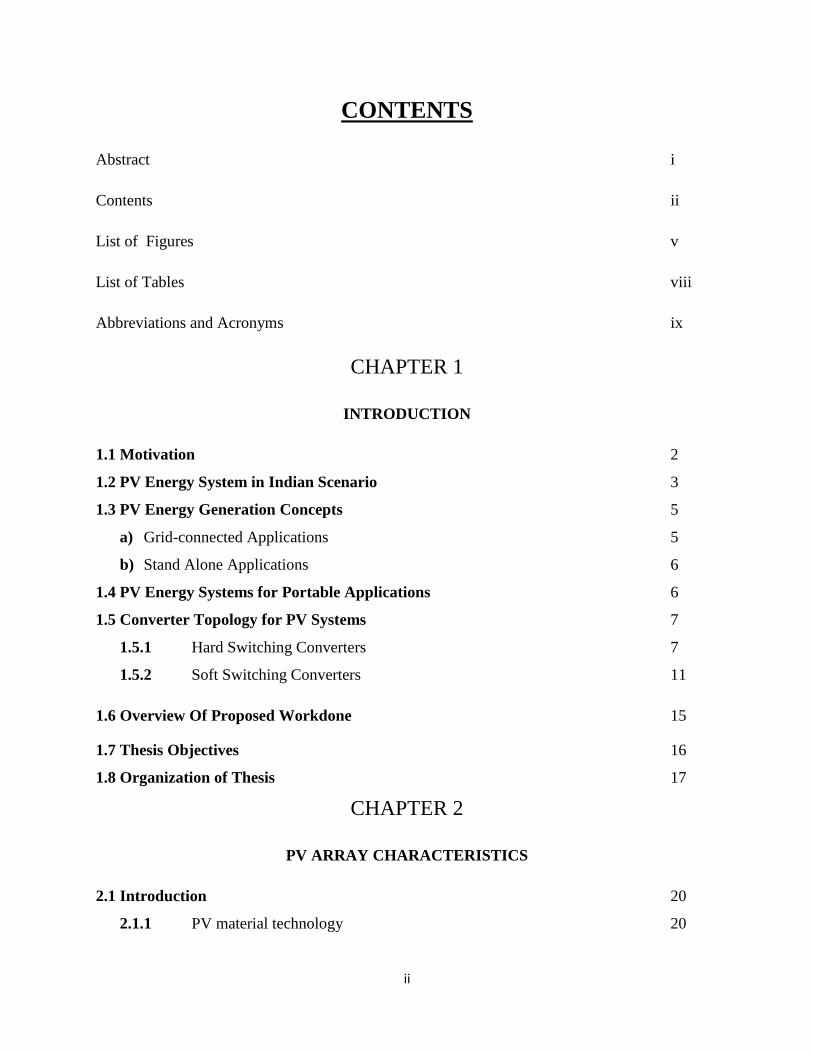
CONTENTS
Abstract i
Contents ii
List of Figures v
List of Tables viii
Abbreviations and Acronyms ix
CHAPTER 1
INTRODUCTION
1.1 Motivation 2
1.2 PV Energy System in Indian Scenario 3
1.3 PV Energy Generation Concepts 5
a) Grid-connected Applications 5
b) Stand Alone Applications 6
1.4 PV Energy Systems for Portable Applications 6
1.5 Converter Topology for PV Systems 7
1.5.1 Hard Switching Converters 7
1.5.2 Soft Switching Converters 11
1.6 Overview Of Proposed Workdone 15
1.7 Thesis Objectives 16
1.8 Organization of Thesis 17
CHAPTER 2
PV ARRAY CHARACTERISTICS
2.1 Introduction 20
2.1.1 PV material technology 20
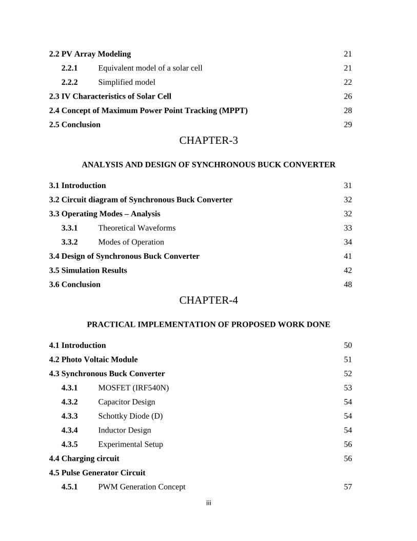
iii
2.2 PV Array Modeling 21
2.2.1 Equivalent model of a solar cell 21
2.2.2 Simplified model 22
2.3 IV Characteristics of Solar Cell 26
2.4 Concept of Maximum Power Point Tracking (MPPT) 28
2.5 Conclusion 29
CHAPTER-3
ANALYSIS AND DESIGN OF SYNCHRONOUS BUCK CONVERTER
3.1 Introduction 31
3.2 Circuit diagram of Synchronous Buck Converter 32
3.3 Operating Modes – Analysis 32
3.3.1 Theoretical Waveforms 33
3.3.2 Modes of Operation 34
3.4 Design of Synchronous Buck Converter 41
3.5 Simulation Results 42
3.6 Conclusion 48
CHAPTER-4
PRACTICAL IMPLEMENTATION OF PROPOSED WORK DONE
4.1 Introduction 50
4.2 Photo Voltaic Module 51
4.3 Synchronous Buck Converter 52
4.3.1 MOSFET (IRF540N) 53
4.3.2 Capacitor Design 54
4.3.3 Schottky Diode (D) 54
4.3.4 Inductor Design 54
4.3.5 Experimental Setup 56
4.4 Charging circuit 56
4.5 Pulse Generator Circuit
4.5.1 PWM Generation Concept 57
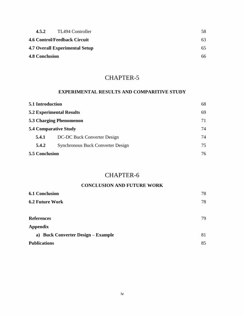
iv
4.5.2 TL494 Controller 58
4.6 Control/Feedback Circuit 63
4.7 Overall Experimental Setup 65
4.8 Conclusion 66
CHAPTER-5
EXPERIMENTAL RESULTS AND COMPARITIVE STUDY
5.1 Introduction 68
5.2 Experimental Results 69
5.3 Charging Phenomenon 71
5.4 Comparative Study 74
5.4.1 DC-DC Buck Converter Design 74
5.4.2 Synchronous Buck Converter Design 75
5.5 Conclusion 76
CHAPTER-6
CONCLUSION AND FUTURE WORK
6.1 Conclusion 78
6.2 Future Work 78
References 79
Appendix
a) Buck Converter Design – Example 81
Publications 85
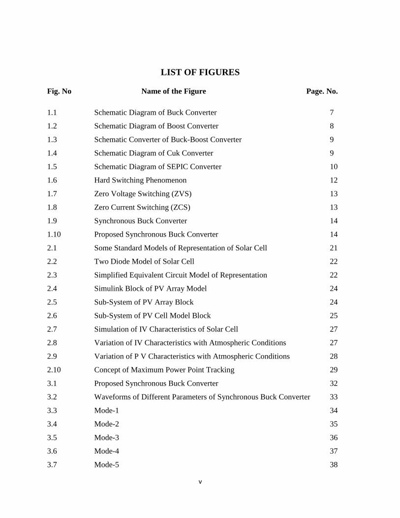
v
LIST OF FIGURES
Fig. No Name of the Figure Page. No.
1.1 Schematic Diagram of Buck Converter 7
1.2 Schematic Diagram of Boost Converter 8
1.3 Schematic Converter of Buck-Boost Converter 9
1.4 Schematic Diagram of Cuk Converter 9
1.5 Schematic Diagram of SEPIC Converter 10
1.6 Hard Switching Phenomenon 12
1.7 Zero Voltage Switching (ZVS) 13
1.8 Zero Current Switching (ZCS) 13
1.9 Synchronous Buck Converter 14
1.10 Proposed Synchronous Buck Converter 14
2.1 Some Standard Models of Representation of Solar Cell 21
2.2 Two Diode Model of Solar Cell 22
2.3 Simplified Equivalent Circuit Model of Representation 22
2.4 Simulink Block of PV Array Model 24
2.5 Sub-System of PV Array Block 24
2.6 Sub-System of PV Cell Model Block 25
2.7 Simulation of IV Characteristics of Solar Cell 27
2.8 Variation of IV Characteristics with Atmospheric Conditions 27
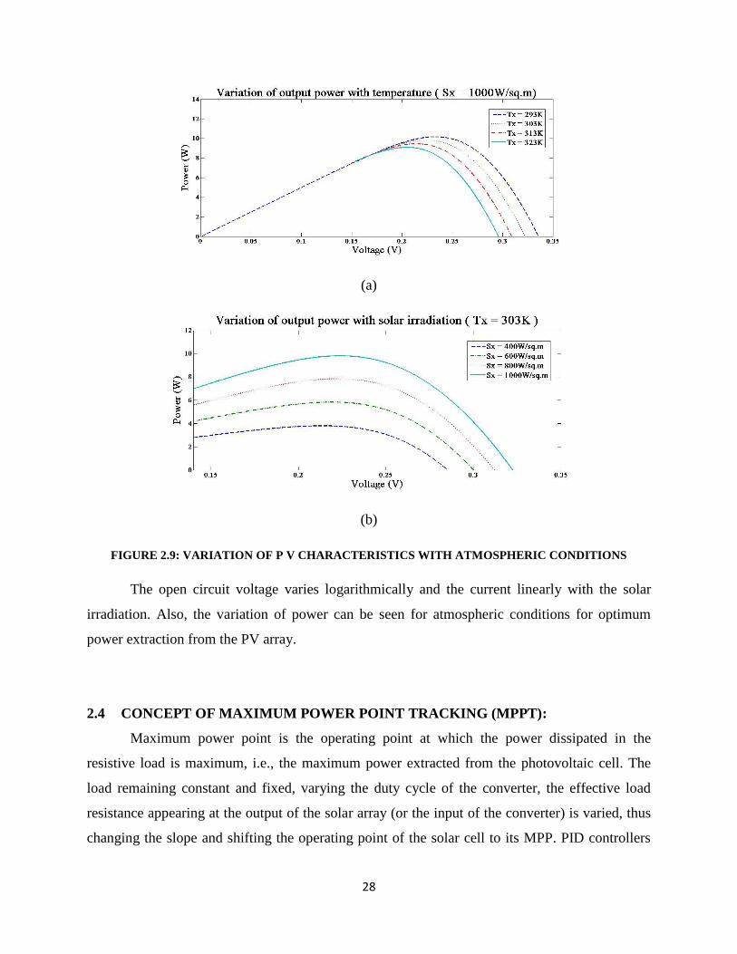
2.9 Variation of P V Characteristics with Atmospheric Conditions 28
2.10 Concept of Maximum Power Point Tracking 29
3.1 Proposed Synchronous Buck Converter 32
3.2 Waveforms of Different Parameters of Synchronous Buck Converter 33
3.3 Mode-1 34
3.4 Mode-2 35
3.5 Mode-3 36
3.6 Mode-4 37
3.7 Mode-5 38
vi
3.8 Mode-6 39
3.9 Mode-7 40
3.10 Mode-8 41
3.11 Over All Diagram of Synchronous Buck Converter
With Feed Back 43
3.12 Internal Circuit of the Sub System 43
3.13 Response of Current flowing through MOSFET „S‟ 44
3.14 Response of Voltage across MOSFET „S‟ 44
3.15 Response of Current flowing through MOSFET „S1‟ 45
3.16 Response of Voltage across MOSFET „S1‟ 45
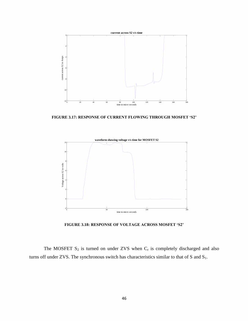
3.17 Response of Current flowing through MOSFET „S2‟ 46
3.18 Response of Voltage across MOSFET „S2‟ 46
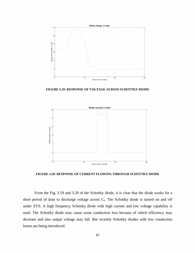
3.19 Response of Voltage across Schottky Diode 47
3.20 Response of Current flowing through Schottky Diode 47
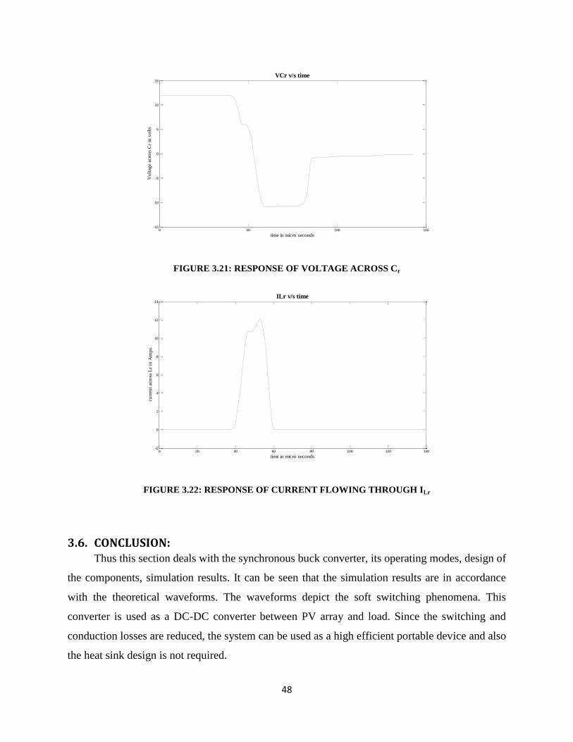
3.21 Response of Voltage across Cr 48
3.22 Response of Current flowing through Ilr 48
4.1 Functional Block Diagram of the PV Energy System 50
4.2 Practical IV Characteristics of the PV Array 51
4.3 Photograph of the Solar Array 52
4.4 Topology of Synchronous Buck Converter 52
4.5 Pin Configuration of IRF540N 53
4.6 Diagram of the Inductor 54
4.7 Practical Model of Synchronous Buck Converter 56
4.8 Circuit Diagram of the Charging Circuit 56
vii
4.9 Generation of PWM Pulse 58
4.10 TL494 Functional Block Diagram 59
4.11 Generation of S1_Pulse Using TL494 61
4.12 Generation of S2_Pulse Using TL494 61
4.13 Master-Slave Drives Using a Single Oscillator Clock 62
4.14 Simulink Block Diagram of Synchronous Pulse Generator 63
4.15 Internal Circuit Diagram of Synchronous Pulse Generator 64
4.16 Overall Circuit Diagram of Pulse Generator 65
4.17 Overall Circuit Diagram of Synchronous Buck Converter 65
4.18 Photograph of the Circuit Made 66
5.1 Complete Experimental Setup for Proposed Work Done 68
5.2 Comparison of Saw Tooth and Control Voltage 69
5.3 Gate Pulse for MOSFET S1 69
5.4 Gate Pulse for MOSFET S2 70
5.5 Gate Pulse for MOSFET S 70
5.6 Output Voltage of DC-DC Buck Converter 71
5.7 Battery Current Vs Time 71
5.8 Battery Voltage Vs Time 72
5.9 Solar Irradiation Vs Time 73
5.10 Temperature Vs Time 73
5.11 Converter Efficiency Comparison 76
viii
LIST OF TABLES
Table. No. Name of the Table Page. No.
1.1 Distribution of Power Generation in India from Different Sources 3
1.2 Hard Switching DC-DC Converter Topologies 11
4.1 Sequence of Switching Operation 62
5.1 Parameters for Design 74
5.2 DC-DC Buck Converter Design 74
5.3 Proposed Synchronous Buck Converter Design 75
ix
ABBREVIATIONS AND ACRONYMS
MNRE - Ministry of New and Renewable Energy
NVVN - NTPC Vidyut Vyapar Nigam
IREDA - Indian Renewable Energy Development Agency
PVA - Photo Voltaic Array
AC - Alternating Current
DC - Direct Current
SPV - Solar Photo Voltaic
MOSFET - Metal Oxide Semiconductor Field Effect Transistor
SEPIC - Single Ended Primary Inductor Converter
PWM - Pulse Width Modulation
EMI - Electro Magnetic Interference
ZVS - Zero Voltage Switching
ZCS - Zero Current Switching
MATLAB - MATrix LABoratory
MPP(T) - Maximum Power Point (Tracking)
PID - Proportional, Integral and Derivative
DSSC - Dye Sensitized Solar Cell
CPV - Concentrated Photo Voltaic
IC - Integrated Circuit
DIP - Dual Inline Package
LED - Light Emitting Diode
SMPS - Switched Mode Power Supply

1
CHAPTER 1
Introduction
2
1.1 MOTIVATION:
The demand for energy is increasing particularly in developing countries like India and
China. Unfortunately, the existing fossil reserves that fuel the conventional power is depleting at
high rate. The unavailability of fossil fuel and increased demand for energy has pushed us
towards finding alternative sources of energy. There are many alternative sources of energy such
as solar, wind, ocean thermal, tidal, biomass, geo-thermal, nuclear energy etc.
The abundance of solar energy present everywhere makes it readily available than any
other source of energy that can be feasibly extracted and utilised. This solar energy can be
converted into electricity with the help of solar panel that are made up of silicon photovoltaic
cells. This ready availability can be utilised opportunistically for portable applications [1]-[2].
Rural India constitutes the major portion of the population which has very limited access to
electricity. Since designing low cost high efficiency solution to generate power in rural areas is
easier with PV systems than most of the other systems available, the project is aimed at
developing low power energy systems for portable applications such as mobile charging, solar
lamps, etc. for use in rural areas.
But owing to the high cost of the production of such panels, and further, small efficiency
delivered by the panels make it a poor competitor in the energy market as a major source of
power generation. However, it is better than the conventional sources of energy when
particularly used for portable power consumption. Also, the technology used to make
photovoltaic cells is improving in efficiency with reduction in costs. Further, the government is
promoting the usage of solar cell by paying attractive feed-in tariff.
Thus, for portable low power applications such as mobile charging, the overall cost can
be reduced by improving the efficiency of the overall system. Since the efficiency of the solar
cell is fixed by the manufacturer‟s technology, the efficiency can be improved by choosing a
converter designed specifically for such systems whose efficiency is higher than that of the
conventional converter designs. This allows smaller usage of solar cell area per watt required and
makes the system light and portable.
3
1.2 PV ENERGY SYSTEM IN INDIAN SCENARIO:
India imports more than 80% of its oil; hence it has a huge dependency on external
sources for development. With depleting fossil reserves worldwide, there has been a threat to
India‟s future energy security. Hence, the government of India is investing huge capital on
development of alternative sources of energy such as solar, small hydroelectric, biogas and wind
energy systems apart from the conventional nuclear and large hydroelectric systems [3].
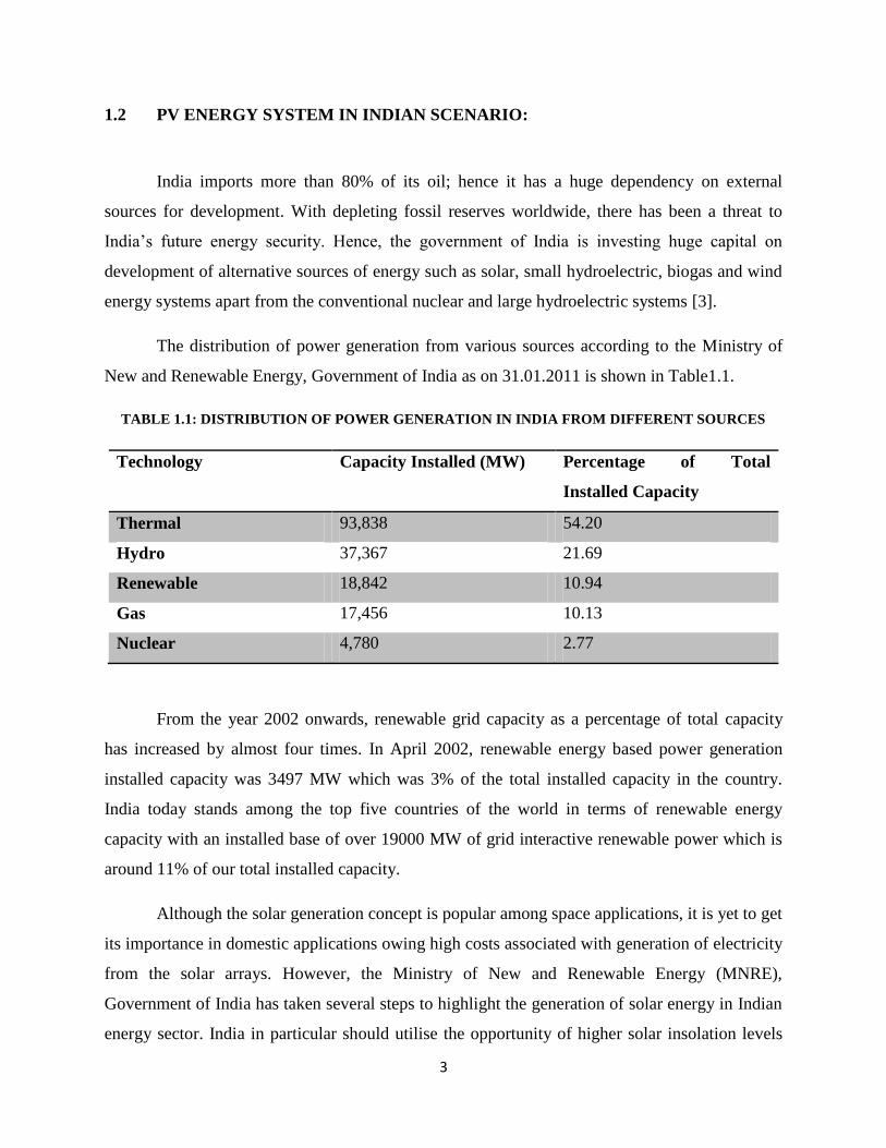
The distribution of power generation from various sources according to the Ministry of
New and Renewable Energy, Government of India as on 31.01.2011 is shown in Table1.1.
TABLE 1.1: DISTRIBUTION OF POWER GENERATION IN INDIA FROM DIFFERENT SOURCES
Technology Capacity Installed (MW) Percentage of Total
Installed Capacity
Thermal 93,838 54.20
Hydro 37,367 21.69
Renewable 18,842 10.94
Gas 17,456 10.13
Nuclear 4,780 2.77
From the year 2002 onwards, renewable grid capacity as a percentage of total capacity
has increased by almost four times. In April 2002, renewable energy based power generation
installed capacity was 3497 MW which was 3% of the total installed capacity in the country.
India today stands among the top five countries of the world in terms of renewable energy
capacity with an installed base of over 19000 MW of grid interactive renewable power which is
around 11% of our total installed capacity.
Although the solar generation concept is popular among space applications, it is yet to get
its importance in domestic applications owing high costs associated with generation of electricity
from the solar arrays. However, the Ministry of New and Renewable Energy (MNRE),
Government of India has taken several steps to highlight the generation of solar energy in Indian
energy sector. India in particular should utilise the opportunity of higher solar insolation levels
4
than most of the countries in the world to harness solar energy. The estimated potential of solar
power that can be harnessed on the surface is 50MW/sq.km.
The ministry of new and renewable energy has given focus mainly of wind power
generation as it is more economical on a large scale production of electricity. However, solar is a
popular substitute where wind energy has to be transmitted over long distances from generation
site to the consumers.
The Indian solar market primarily consisted of solar water heaters, solar cookers, etc.
With improved technology of solar cells, there has been a rise in the consumption of this energy
system in various organisations such as Indian railways. The railways are using them for
electrification of tracks, manned level crossings, canteens, etc. The modern architectural designs
make provision for photovoltaic cells and necessary circuitry for independent power generation
with aesthetic design.
The current contribution of solar energy power generation through photovoltaic systems
is 37.66MW (up to 31.03.2011). The estimated power generation from solar was set by MNRE
as 200MW by the end of 2011. The MNRE has approved Jawaharlal Nehru National Solar
Mission, whose resolution is to develop and deploy the solar energy technologies in the country
to achieve parity with the grid tariff by 2022. To achieve the target of 20 GW by 2022, the
mission is focussed on increasing the production of grid-connected solar energy of 1000MW by
2013. The Ministry issued guidelines for (i) new grid projects through NVVN, (ii) small grid
projects through IREDA, (iii) off-grid solar applications; and (iv) technical performance and
domestic content requirements of solar projects, to operationalize the Solar Mission. Projects
under each of the separate schemes have been sanctioned for implementation, leading to capacity
addition of more than 17 MWp during the year and sanction of 804 MW of grid connected
projects and 32 MW of off-grid projects.
Hence, as the first step, the mission is focussed on promoting off-grid power generation
for homes which reduces the dependency on the grid. The solar energy developers will be
bundled with the conventional power in the form of bundled energy transmission. The proposed
solar power generation for the year 2011-2012 is set by the mission at 150MW.
5
Thus, various projects are taken all over the country by MNRE and the state government
departments such as Maharashtra Energy Development Agency to harness solar power through
photovoltaic cell systems and solar thermal systems. The financial assistance to such projects is
being promoted by the government through Indian Renewable Energy Development Agency
(IREDA), a public sector company with a motto “ENERGY FOR EVER”.
A low power stand-alone solar generation system of capacity of 250KWh per month
would cost around Rs.5 lakhs (as per taxes in year 2010-11). The present cost of electricity
generation from solar thermal and solar photovoltaic energy systems is 15.31 and 17.91 per
unit, respectively as fixed by Central Electricity Regulatory Commission.
1.3 PV ENERGY GENERATION CONCEPTS:
1.3.1 Grid-Connected Applications:
In this mode of solar power generation, the solar arrays are used in huge capacities of the
order of MW to generate bulk power at the solar farms, which is coupled through an inverter to
the grid and feeds in power that synchronises with the conventional power in the grid. The grid
connected solar power operates at 33KV and at 50 Hz frequency through inverter systems,
whereas the solar farms generate the average power output of about 5MW each. Owing to very
high power generation, the batteries are not used to store power as in case of isolated power
generation for economic concerns. 53 grid-connected solar projects were selected up to the end
of 2010 comprising of total capacity of 704MW.
NTPC Vidyut Vyapar Nigam (NVVN), the trading subsidiary of NTPC, was identified as
the implementing agency for grid connected solar power generation. NVVN was allowed to
purchase solar power from the project developers and bundle with power from the cheaper
unallocated quota of the Government of India (Ministry of Power) out of the NTPC coal based
stations and selling this “bundled” power to Distribution Utilities. NVVN invited Expressions of
Interest in August, 2010 to select 150 MW of Solar PV projects and 470 MW solar thermal
projects, which yielded huge response by way of an offer of more than 5,000 MW.
6
1.3.2 Stand Alone Applications:
This mode of energy generation from solar consists of systems which are not connected
to the grid, i.e. off-grid applications (captive power). It is done especially in the north-eastern
states and several districts of Rajasthan, where there is scarce of electricity from the conventional
sources. These stand-alone systems have a solar array, coupled with a power conditioning
devices such as an inverter that converts the power from DC to AC to suit the load requirements
such as home power and a battery to store the solar energy harnessed during the day to consume
it in the absence of solar energy. These decentralised systems of PV array operate at below
33KV and 50Hz through the inverter. However, the larger capacities of the order of KW usually
sell the power to grid and get paid with attractive tariff. The heating systems concentrate the sun
rays on heating water which can be used for cooking, washing, power generation, etc.
About 8.2 lakhs solar lanterns, 6.7 lakhs solar home lighting systems, 1.2 lakhs solar
street lighting systems, 7,495 solar water pumping systems, stand-alone and grid connected solar
photovoltaic (SPV) power plants of about 4MWp capacity, about 3.97 million square meter solar
water heater collector area and 6.39 lakhs solar cookers have been distributed/installed in the
country, as on 31.01.2011.
1.4 PV ENERGY SYSTEMS FOR PORTABLE APPLICATIONS:
This energy generation system consists mostly of capacities below 100W. They have a
huge range of applications ranging from powering calculators, educational toys, solar lamps,
traffic signals, mobile chargers, etc. They are usually made up of poly crystalline material of
solar cells due to their higher energy density over a small area and fits in the portable
applications. However, this system is not highly commercialised due to battery technology
required to store the power generated and high cost of poly crystalline silicon solar cells. They
generally use lithium ion batteries [4] to store energy due to its high energy capacity and light in
weight. These systems come handy when power is required on move and has a potential to
revolutionise the current era of electronics with free power on move. The simple mobile charger
based on PV energy system consists of a small solar module generally made of poly crystalline
7
silicon, connected to the electrical load through a buck/boost converter for regulation of voltage
at the load end [5]. This regulation is usually done using a feedback loop that senses the output
voltage and tries to keep it at the desired output voltage required.
1.5 CONVERTER TOPOLOGY FOR PV SYSTEMS:
1.5.1 Hard Switching Converters:
a. Introduction:
Hard Switching converters comprise of those converters which obeys the conventional
switching phenomenon. While the switch is turned ON, the voltage across the switch tends to
decrease and the current across the switch tends to increase. This results in some switching
losses. Alike to turning ON, when the switch is turned OFF, the current through the switch
tends to decrease and the voltage across its terminals tends to increase. This too results in
switching losses.
There are several topologies [6] of these conventional hard switching converters of which we
discuss mainly 6 types of converters:
i. Buck Converter
ii. Boost Converter
iii. Buck – Boost Converter
iv. Ćuk Converter
v. SEPIC Converter
i. Buck Converter:
FIGURE 1.1: SCHEMATIC DIAGRAM OF BUCK CONVERTER
8
Buck Converter is also known as Step-down Converter. When the MOSFET switch is ON,
the voltage across the load is Vs. The current flowing through the load is same as shown in the
diagram. When the MOSFET switch is turned off, the current through the load is in the same
direction as mentioned but the voltage across the load is zero. The power is flowing from source
to load. Therefore, the average voltage across the load is less than the source voltage, which is
determined by the duty cycle of the pulse provided to the MOSFET switch.
The inductor is used to smoothen the load current and make it a DC current and, the
capacitor is used to reduce the ripples of the output voltage and supply a steady voltage.
ii. Boost Converter:
FIGURE 1.2: SCHEMATIC DIAGRAM OF BOOST CONVERTER
Boost Converter is a DC-DC converter for which output voltage is greater than input
voltage. When the MOSFET switch is ON, the current through the inductor increases and the
inductor starts to store energy. When the MOSFET switch is closed, the energy stored in the
inductor starts dissipating. The current from the voltage source and the inductor flows through
the fly back Diode D to the load. The Voltage across the load is greater than the input voltage
and is dependent on the rate of change of the inductor current.
Thus the average voltage across the load is greater than the input voltage and is
determined with help of the duty cycle of the gate pulse to the MOSFET switch.
9
iii. Buck-Boost Converter:
FIGURE 1.3: SCHEMATIC CONVERTER OF BUCK-BOOST CONVERTER
Buck-Boost Converter is a DC -to- DC Converter of which output voltage is either
greater than or less than the input voltage. When the MOSFET switches are ON, the input
voltage is across the inductor. Thus the inductor starts accumulating energy. When the MOSFET
switches are OFF, the energy stored in the inductor is supplied to the load and the capacitor.
Therefore the output voltage can be varied based on the duty cycle of the gate pulse to the
MOSFET switches. Buck – Boost converter behaves both as a buck and a boast converter
depending of the duty cycle of the pulse.
iv. Ćuk Converter:
FIGURE 1.4: SCHEMATIC DIAGRAM OF CUK CONVERTER
10
Same as the Buck – Boost Converter, Cuk converter output voltage is either greater than
or less than the input voltage. But, the main energy storage element is capacitor unlike the
inductor in other converters. Capacitor is alternately connected to the input and the output thus
transferring the electrical energy. When the MOSFET switch is OFF, the capacitor is charged by
the input voltage through the inductor, L1. When the MOSFET switch is ON, the energy stored
in the capacitor discharges to the load through the output inductor, L2.
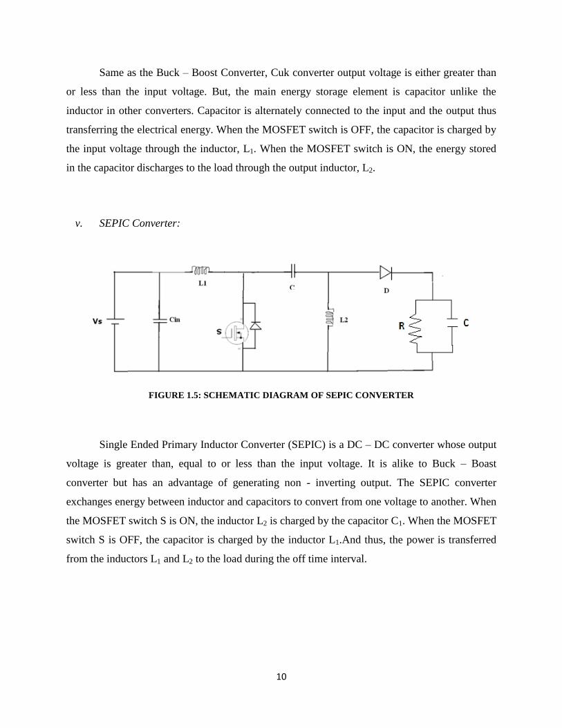
v. SEPIC Converter:
FIGURE 1.5: SCHEMATIC DIAGRAM OF SEPIC CONVERTER
Single Ended Primary Inductor Converter (SEPIC) is a DC – DC converter whose output
voltage is greater than, equal to or less than the input voltage. It is alike to Buck – Boast
converter but has an advantage of generating non - inverting output. The SEPIC converter
exchanges energy between inductor and capacitors to convert from one voltage to another. When
the MOSFET switch S is ON, the inductor L2 is charged by the capacitor C1. When the MOSFET
switch S is OFF, the capacitor is charged by the inductor L1.And thus, the power is transferred
from the inductors L1 and L2 to the load during the off time interval.
11
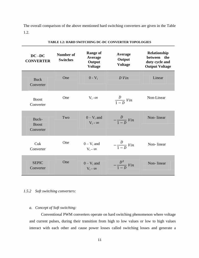
The overall comparison of the above mentioned hard switching converters are given in the Table
1.2.
TABLE 1.2: HARD SWITCHING DC-DC CONVERTER TOPOLOGIES
DC –DC
CONVERTER
Number of
Switches
Range of
Average
Output
Voltage
Average
Output
Voltage
Relationship
between the
duty cycle and
Output Voltage
Buck
Converter
One
0 - Vi
Linear
Boost
Converter
One
Vi -
Non-Linear
Buck-
Boost
Converter
Two
0 – Vi and
Vi -
Non- linear
Cuk
Converter
One
0 – Vi and
Vi -
Non- linear
SEPIC
Converter
One
0 – Vi and
Vi -
Non- linear
1.5.2 Soft switching converters:
a. Concept of Soft switching:
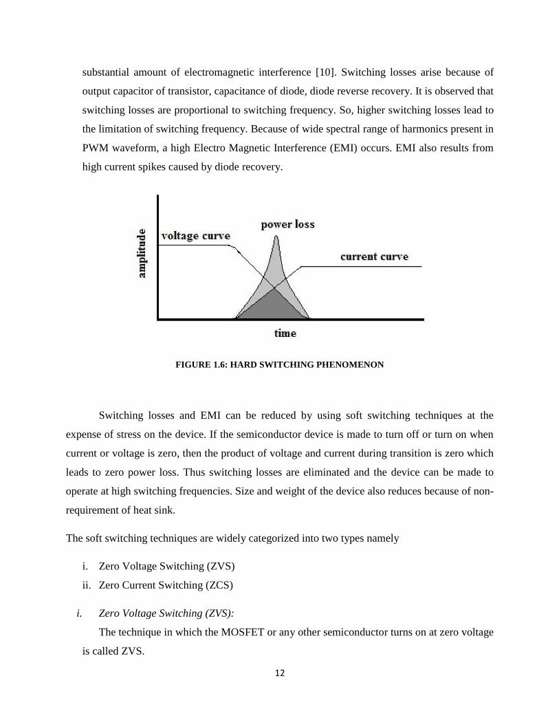
Conventional PWM converters operate on hard switching phenomenon where voltage
and current pulses, during their transition from high to low values or low to high values
interact with each other and cause power losses called switching losses and generate a
12
substantial amount of electromagnetic interference [10]. Switching losses arise because of
output capacitor of transistor, capacitance of diode, diode reverse recovery. It is observed that
switching losses are proportional to switching frequency. So, higher switching losses lead to
the limitation of switching frequency. Because of wide spectral range of harmonics present in
PWM waveform, a high Electro Magnetic Interference (EMI) occurs. EMI also results from
high current spikes caused by diode recovery.
FIGURE 1.6: HARD SWITCHING PHENOMENON
Switching losses and EMI can be reduced by using soft switching techniques at the
expense of stress on the device. If the semiconductor device is made to turn off or turn on when
current or voltage is zero, then the product of voltage and current during transition is zero which
leads to zero power loss. Thus switching losses are eliminated and the device can be made to
operate at high switching frequencies. Size and weight of the device also reduces because of non-
requirement of heat sink.
The soft switching techniques are widely categorized into two types namely
i. Zero Voltage Switching (ZVS)
ii. Zero Current Switching (ZCS)
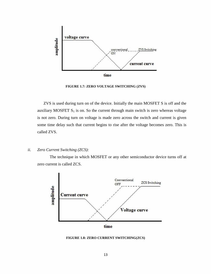
i. Zero Voltage Switching (ZVS):
The technique in which the MOSFET or any other semiconductor turns on at zero voltage
is called ZVS.
13
FIGURE 1.7: ZERO VOLTAGE SWITCHING (ZVS)
ZVS is used during turn on of the device. Initially the main MOSFET S is off and the
auxiliary MOSFET S1 is on. So the current through main switch is zero whereas voltage
is not zero. During turn on voltage is made zero across the switch and current is given
some time delay such that current begins to rise after the voltage becomes zero. This is
called ZVS.
ii. Zero Current Switching (ZCS):
The technique in which MOSFET or any other semiconductor device turns off at
zero current is called ZCS.
FIGURE 1.8: ZERO CURRENT SWITCHING(ZCS)
14
ZCS is used during turn off of the device. Initially the device is conducting. So the
current passing through the device is not zero and the voltage across the device is zero. In the
ZCS condition, current is made zero and the voltage is made to rise only after the current
becomes zero. Thus there is no power loss during turn off of the device.
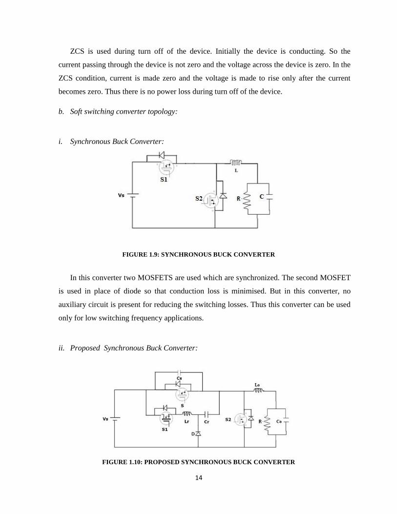
b. Soft switching converter topology:
i. Synchronous Buck Converter:
FIGURE 1.9: SYNCHRONOUS BUCK CONVERTER
In this converter two MOSFETS are used which are synchronized. The second MOSFET
is used in place of diode so that conduction loss is minimised. But in this converter, no
auxiliary circuit is present for reducing the switching losses. Thus this converter can be used
only for low switching frequency applications.
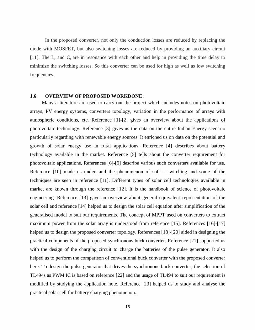
ii. Proposed Synchronous Buck Converter:
FIGURE 1.10: PROPOSED SYNCHRONOUS BUCK CONVERTER
15
In the proposed converter, not only the conduction losses are reduced by replacing the
diode with MOSFET, but also switching losses are reduced by providing an auxiliary circuit
[11]. The Lr and Cr are in resonance with each other and help in providing the time delay to
minimize the switching losses. So this converter can be used for high as well as low switching
frequencies.
1.6 OVERVIEW OF PROPOSED WORKDONE:
Many a literature are used to carry out the project which includes notes on photovoltaic
arrays, PV energy systems, converters topology, variation in the performance of arrays with
atmospheric conditions, etc. Reference [1]-[2] gives an overview about the applications of
photovoltaic technology. Reference [3] gives us the data on the entire Indian Energy scenario
particularly regarding with renewable energy sources. It enriched us on data on the potential and
growth of solar energy use in rural applications. Reference [4] describes about battery
technology available in the market. Reference [5] tells about the converter requirement for
photovoltaic applications. References [6]-[9] describe various such converters available for use.
Reference [10] made us understand the phenomenon of soft – switching and some of the
techniques are seen in reference [11]. Different types of solar cell technologies available in
market are known through the reference [12]. It is the handbook of science of photovoltaic
engineering. Reference [13] gave an overview about general equivalent representation of the
solar cell and reference [14] helped us to design the solar cell equation after simplification of the
generalised model to suit our requirements. The concept of MPPT used on converters to extract
maximum power from the solar array is understood from reference [15]. References [16]-[17]
helped us to design the proposed converter topology. References [18]-[20] aided in designing the
practical components of the proposed synchronous buck converter. Reference [21] supported us
with the design of the charging circuit to charge the batteries of the pulse generator. It also
helped us to perform the comparison of conventional buck converter with the proposed converter
here. To design the pulse generator that drives the synchronous buck converter, the selection of
TL494s as PWM IC is based on reference [22] and the usage of TL494 to suit our requirement is
modified by studying the application note. Reference [23] helped us to study and analyse the
practical solar cell for battery charging phenomenon.

16
1.7 THESIS OBJECTIVES:
The following objectives are hopefully to be achieved at the end of the project.
1) To study the solar cell model and observe its characteristics.
2) To study the proposed synchronous DC-DC buck converter and its operation.
3) To study the pulse generation and regulation of the controller output through feedback.
4) To study the comparison between the conventional DC-DC buck converter and the
proposed synchronous DC-DC buck converter in terms of efficiency improvement and
switching loss reduction.
5) To validate the experimental results obtained from the laboratory set-up and to analyse
the results with the simulated results in the MATLAB-Simulink Environment.
17
1.8 ORGANISATION OF THESIS:
The thesis is organised into six chapters including the chapter of introduction. Each
chapter is different from the other and is described along with the necessary theory required to
comprehend it.
Chapter2 deals with PV Array Characteristics and its modelling. First, the solar cell is
described and various material technologies available for construction of solar cells are seen. The
equivalent mathematical modelling of the solar cell is made after studying various
representations and simplification is made for our purpose. The IV characteristics curve for the
equivalent model is studied in MATLAB-Simulink environment using the equation
corresponding to that model. Also, the concept of MPPT is studied theoretically to understand
the role of converter in extracting the maximum power from the solar array with the help of
MPPT controller. The IV characteristics of solar cell are obtained and including the effect of
temperature and ambient solar insolation, the variation in the IV characteristics are studied.
Chapter3 describes the design of synchronous buck converter and analysis of its
operation. The concept of synchronous buck converter is understood and the topology of
synchronous buck converter used is shown. The modes of operation of the topology of the
converter used are studied. The theoretical waveforms of voltage and current across various
components are drawn to get a better understanding of the modes of operation. The equations
corresponding to these modes of operation are analysed for designing the components of the
synchronous buck converter. The values of resonant inductor, capacitor and the selection of
MOSFET are made depending on these values so that proper operation is possible. Finally, the
simulation results that represent the characteristics of the synchronous buck converter are
simulated in the MATLAB-Simulink environment using the calculated values of the components
in the converter.
Chapter4 shows the practical implementation of the converter obtained from the
simulated model. The basic blocks required in the actual model are first studied. They are first
divided into five blocks for convenience. They are PV module, Synchronous buck converter
module, charging circuit module, pulse generator module, feedback control module and the load.
18
PV module deals with study of an actual solar cell and analyse its characteristics. Synchronous
buck converter module deals with designing of resonant inductor and capacitor and the
characteristics of the MOSFET used in practical design is studied. The charging circuit module
tells about the type of battery used and the method of charging the battery which drives the pulse
generator circuit. The pulse generator module gives the picture of the generator circuit deigned
for generating the required pulses for operation using TL-494s. The Simulink model of PID
control is studied here for feedback control. Then, the overall experimental setup is charted out
for open loop configuration of the converter.
Chapter5 presents the experimental results of the pulse generator output for driving the
synchronous buck converter. The output voltage and current waveforms for a conventional buck
converter is also shown. The charging phenomenon of the PV module used is studied to know
the output voltage, current and power from the module over a long period of time of the day. The
charging phenomenon is studied for different configurations. Then, a comparative study is made
on the theoretical efficiency of synchronous buck converter with that of the conventional buck
converter.
Chapter6 concludes the work performed so far. The possible limitations in proceeding
research towards this work are discussed. The future work that can be done in improving the
current scenario is mentioned. The future potential along the lines of this work is also discussed.

19
CHAPTER 2
PV ARRAY
CHARACTERISTICS
20
2.1 INTRODUCTION:
The PV cell is made up of silicon PN junction (hetero junction) where the N-junction is
exposed to the incident solar radiation. The flow of current from the solar cell is due to electrons
displaced from the PN junction by the incident photons of solar irradiation. The junction reverse
voltage determines the total voltage output from the cell. Usually, the amount of solar power
from a single chip is very small of the order of milli-watts. Hence the solar cells are usually
connected in series and parallel combinations to build up voltage and current respectively. Thus
it gives rise to the desired output voltage delivering he required load current.
The performance of the solar cell depends on the manufacturing material used, fabrication
techniques implemented, atmospheric conditions and load demand. The performance is usually
studied by measuring the output characteristics graph of the PV cell over different temperatures
and solar insolation levels.
2.1.1 PV Material Technology:
Solar cell materials are the deciding factors for efficiency, energy density, manufacturing
cost, output cost, etc. initially, the solar cells were manufactured using germanium compounds
and copper sulphides. Later on, the focus shifted towards making silicon solar cells [12].
Mono crystalline silicon cells were layers of pure silicon whose efficiency was less (about
17%) and cost is more due to process of extraction of pure silicon. They are improved in
efficiency by using multi crystalline silicon ingots. There is also relatively less popular range of
silicon cells called amorphous silicon cells where the amorphous structure of silicon is deposited
on the substrate and doping agents are added to it. They are flexible cells in the form of silicon
ribbon whose efficiency is very less (less than 10%) compared to its crystalline counterparts.
Smaller and more efficient thin film solar modules are made using poly crystalline materials
using different materials whose cost is relatively lesser and work for longer periods.
21
To reduce the dependency on silicon for high manufacturing costs, compromise is made on
the efficiency but at very low costs of construction using new materials. They are dye-sensitized,
organic and nano materials used in the place of silicon but with reduced efficiency (about 5-
10%). Dye-sensitized solar cells (DSSCs) are photo electrochemical cells consisting of a photo
electrode, a redox electrolyte and a counter electrolyte. It is more a photosynthetic cell which is
solid- liquid for operation. In the sensitization process, photosensitizers adsorbed onto the
semiconductor surface absorb visible light and excited electrons are injected into the conduction
band of the semiconductor electrodes. Dye-sensitized oxide semiconductor photoelectrodes have
been used for photo electrochemical cells. The photo electrode generally used is TiO2 due to its
easy construction and non-toxicity and Ru complex is used as its photo sensitizer. The efficiency
of DSSC is found out to be about 10%.
Also, rather than changing material used for construction i.e., silicon, the focus has also
shifted towards making efficient structure of the casing to focus maximum solar irradiation on
the silicon area using focussing lenses and glass. This reduces the area of silicon required to
generate same amount of power, thus reducing the overall cost of the cell. This category of cells
is called Concentrated Photo Voltaic Cells. However, CPV cells require high degree of accuracy
in tracking the solar rays and tracking system is a bit expensive on the downside.
2.2. PV ARRAY MODELLING:
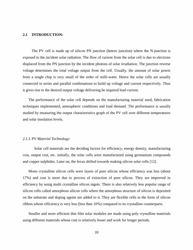
2.2.1 Equivalent model of a solar cell:
FIGURE 2.1: SOME STANDARD MODELS OF REPRESENTATION OF SOLAR CELL
22
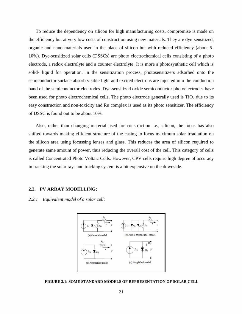
The simplest equivalent representation of a solar cell [13] consists of a photocurrent
source, whose value depends on the solar insolation. A diode in parallel with current source is
taken into account as the solar cell behaves like a diode in darkness or in absence of light. A
series resistance is included to take into account the internal losses due to the current flow. A
shunt resistance in parallel with the photocurrent source is considered for the leakage current to
the ground.
A more accurate model of a solar cell includes another diode in parallel with the photo
current source to account the non-resistive path during recombination of electron hole pair in the
depletion region of the solar cell. But generally, this effect is negligible and thus, is usually not
accounted for to simplify the calculations.
FIGURE 2.2:TWO DIODE MODEL OF SOLAR CELL
2.2.2 Simplified model:
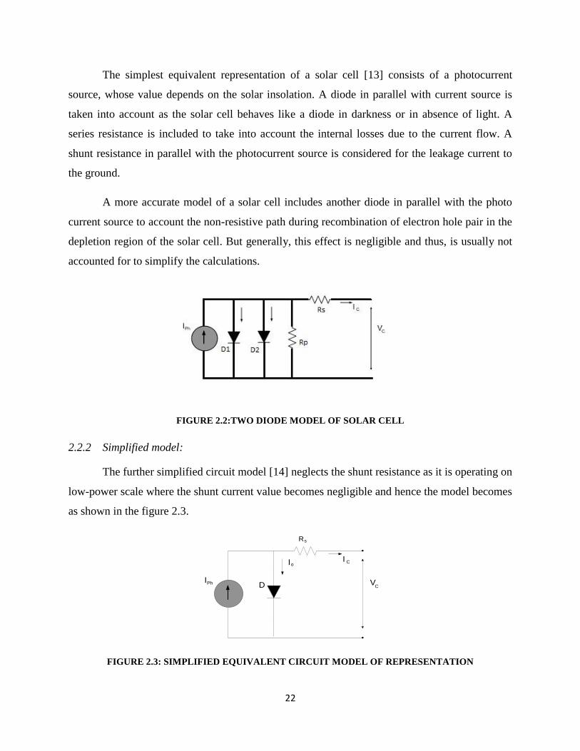
The further simplified circuit model [14] neglects the shunt resistance as it is operating on
low-power scale where the shunt current value becomes negligible and hence the model becomes
as shown in the figure 2.3.
IoI C
IPh
Rs
VCD
FIGURE 2.3: SIMPLIFIED EQUIVALENT CIRCUIT MODEL OF REPRESENTATION
23
The voltage equation for solar cell for the given simplified circuit becomes as in equation (1).
(
) (1)
Where,
: Cell output voltage
A: curve fitting factor (=1)
k: Boltzmann‟s constant (=1.38x10⁻²³
J/K)
Tc: reference temperature (=293K)
e: electron charge (=1.602x10⁻¹⁹
C)
Rs: series resistance of the cell (=0.001A)
Io: reverse saturation current of diode (=0.0002A)
I‟ph: photocurrent, which is a function of temperature and irradiation.
Icell: load current drawn from a single cell.
The benchmark reference output photocurrent (Iph) of 5A obtained at a temperature (Tc)
of 200C and solar irradiation (Sc) of 100W/m
2 is used. The modeling of the simplified equation
of a single solar cell is performed in Simulink environment as shown here.
The overall block diagram of the solar cell can be seen with input values of temperature
Tx and solar irradiation Sx , Number of cells in series Ns and parallel Np in the solar panel. The
output voltage from the PVA model is sent to the load and corresponding set of data of voltage
and current output from the solar panel is measured.
24
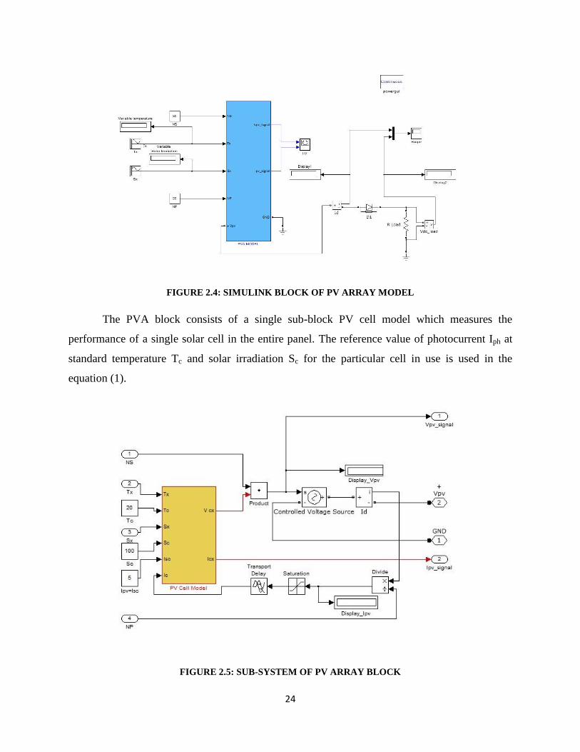
FIGURE 2.4: SIMULINK BLOCK OF PV ARRAY MODEL
The PVA block consists of a single sub-block PV cell model which measures the
performance of a single solar cell in the entire panel. The reference value of photocurrent Iph at
standard temperature Tc and solar irradiation Sc for the particular cell in use is used in the
equation (1).
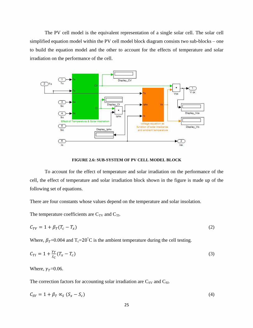
FIGURE 2.5: SUB-SYSTEM OF PV ARRAY BLOCK
25
The PV cell model is the equivalent representation of a single solar cell. The solar cell
simplified equation model within the PV cell model block diagram consists two sub-blocks – one
to build the equation model and the other to account for the effects of temperature and solar
irradiation on the performance of the cell.
FIGURE 2.6: SUB-SYSTEM OF PV CELL MODEL BLOCK
To account for the effect of temperature and solar irradiation on the performance of the
cell, the effect of temperature and solar irradiation block shown in the figure is made up of the
following set of equations.
There are four constants whose values depend on the temperature and solar insolation.
The temperature coefficients are CTV and CTI.
(2)
Where, =0.004 and Tc= C is the ambient temperature during the cell testing.
(3)
Where, =0.06.
The correction factors for accounting solar irradiation are CSV and CSI.
(4)
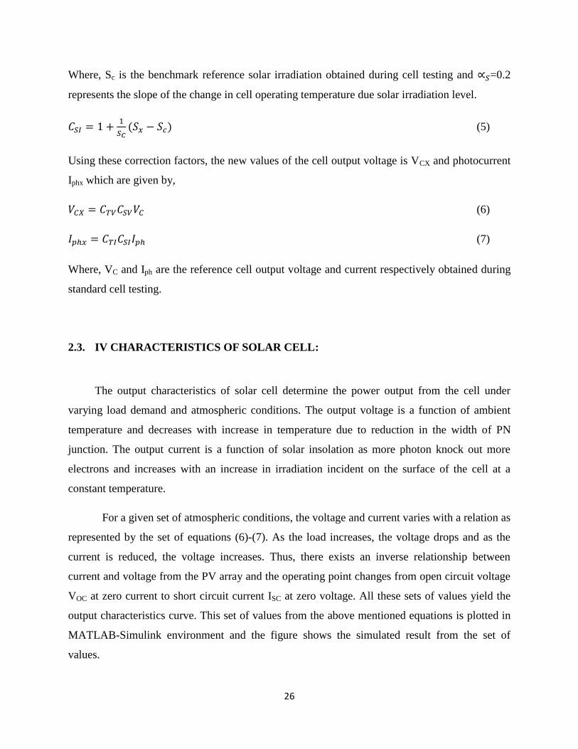
26
Where, Sc is the benchmark reference solar irradiation obtained during cell testing and =0.2
represents the slope of the change in cell operating temperature due solar irradiation level.
(5)
Using these correction factors, the new values of the cell output voltage is VCX and photocurrent
Iphx which are given by,
(6)
(7)
Where, VC and Iph are the reference cell output voltage and current respectively obtained during
standard cell testing.
2.3. IV CHARACTERISTICS OF SOLAR CELL:
The output characteristics of solar cell determine the power output from the cell under
varying load demand and atmospheric conditions. The output voltage is a function of ambient
temperature and decreases with increase in temperature due to reduction in the width of PN
junction. The output current is a function of solar insolation as more photon knock out more
electrons and increases with an increase in irradiation incident on the surface of the cell at a
constant temperature.
For a given set of atmospheric conditions, the voltage and current varies with a relation as
represented by the set of equations (6)-(7). As the load increases, the voltage drops and as the
current is reduced, the voltage increases. Thus, there exists an inverse relationship between
current and voltage from the PV array and the operating point changes from open circuit voltage
VOC at zero current to short circuit current ISC at zero voltage. All these sets of values yield the
output characteristics curve. This set of values from the above mentioned equations is plotted in
MATLAB-Simulink environment and the figure shows the simulated result from the set of
values.
27
FIGURE 2.7: SIMULATION OF IV CHARACTERISTICS OF SOLAR CELL
Also, the variation of the characteristics can be seen for varying sets of temperature and
solar irradiation. Whereas, the dominant effect of increasing cell‟s temperature is the linear
decrease in the open circuit voltage, reducing the cell‟s efficiency. However, the cell output
current increases slightly with increase in the cell temperature.
(a)
(b)
FIGURE 2.8: VARIATION OF IV CHARACTERISTICS WITH ATMOSPHERIC CONDITIONS
28
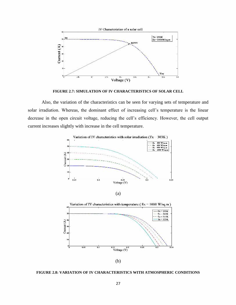
(a)
(b)
FIGURE 2.9: VARIATION OF P V CHARACTERISTICS WITH ATMOSPHERIC CONDITIONS
The open circuit voltage varies logarithmically and the current linearly with the solar
irradiation. Also, the variation of power can be seen for atmospheric conditions for optimum
power extraction from the PV array.
2.4 CONCEPT OF MAXIMUM POWER POINT TRACKING (MPPT):
Maximum power point is the operating point at which the power dissipated in the
resistive load is maximum, i.e., the maximum power extracted from the photovoltaic cell. The
load remaining constant and fixed, varying the duty cycle of the converter, the effective load
resistance appearing at the output of the solar array (or the input of the converter) is varied, thus
changing the slope and shifting the operating point of the solar cell to its MPP. PID controllers
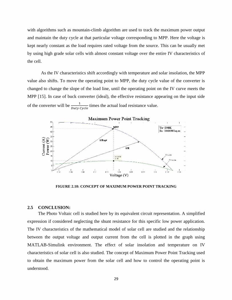
29
with algorithms such as mountain-climb algorithm are used to track the maximum power output
and maintain the duty cycle at that particular voltage corresponding to MPP. Here the voltage is
kept nearly constant as the load requires rated voltage from the source. This can be usually met
by using high grade solar cells with almost constant voltage over the entire IV characteristics of
the cell.
As the IV characteristics shift accordingly with temperature and solar insolation, the MPP
value also shifts. To move the operating point to MPP, the duty cycle value of the converter is
changed to change the slope of the load line, until the operating point on the IV curve meets the
MPP [15]. In case of buck converter (ideal), the effective resistance appearing on the input side
of the converter will be
times the actual load resistance value.
FIGURE 2.10: CONCEPT OF MAXIMUM POWER POINT TRACKING
2.5 CONCLUSION:
The Photo Voltaic cell is studied here by its equivalent circuit representation. A simplified
expression if considered neglecting the shunt resistance for this specific low power application.
The IV characteristics of the mathematical model of solar cell are studied and the relationship
between the output voltage and output current from the cell is plotted in the graph using
MATLAB-Simulink environment. The effect of solar insolation and temperature on IV
characteristics of solar cell is also studied. The concept of Maximum Power Point Tracking used
to obtain the maximum power from the solar cell and how to control the operating point is
understood.
30
CHAPTER 3
Analysis and Design of
Synchronous Buck Converter
31
3.1 INTRODUCTION:
Synchronous buck converter finds its major use in low power applications as a rectifier
because of its high efficiency and low consumption of area. The name synchronous buck
converter is derived from the concept of synchronizing the pulses of MOSFET S and S1 by using
resonance of Lr and Cr [16]. It is also called as synchronous rectifier. It is a DC-DC converter
which gives high efficiency because of its reduced conduction and switching losses. The
conduction losses can be reduced by replacing the diode with a low resistance path provided by
the MOSFET. In order to reduce the switching losses, the auxiliary inductor and capacitor
operate in resonance with each other, thus giving it the name resonant converter. The soft
switching techniques employed for smooth transition of voltage and current through the
MOSFET are Zero Voltage Switching (ZVS) and Zero Current Switching (ZCS). The switching
losses and Electromagnetic Interference (EMI) occurs only during switch on and switch off cases
of the synchronous buck converter. Three different non ideal commutation phenomena are
proposed when MOSFETS are used as power switches [17].
1) The surge current resulted from the reverse recovery current of the freewheeling diode
flows through MOSFET during turn on period. This is the dominant part of EMI and
switching loss.
2) The parasitic drain – source capacitance of the MOSFET discharges during the turn ON
process. This mechanism has to be reduced by resonant converter phenomenon or by
active snubbers.
3) During turn OFF, there is a fast increase in Drain- Source voltage which is the source for
EMI.
32
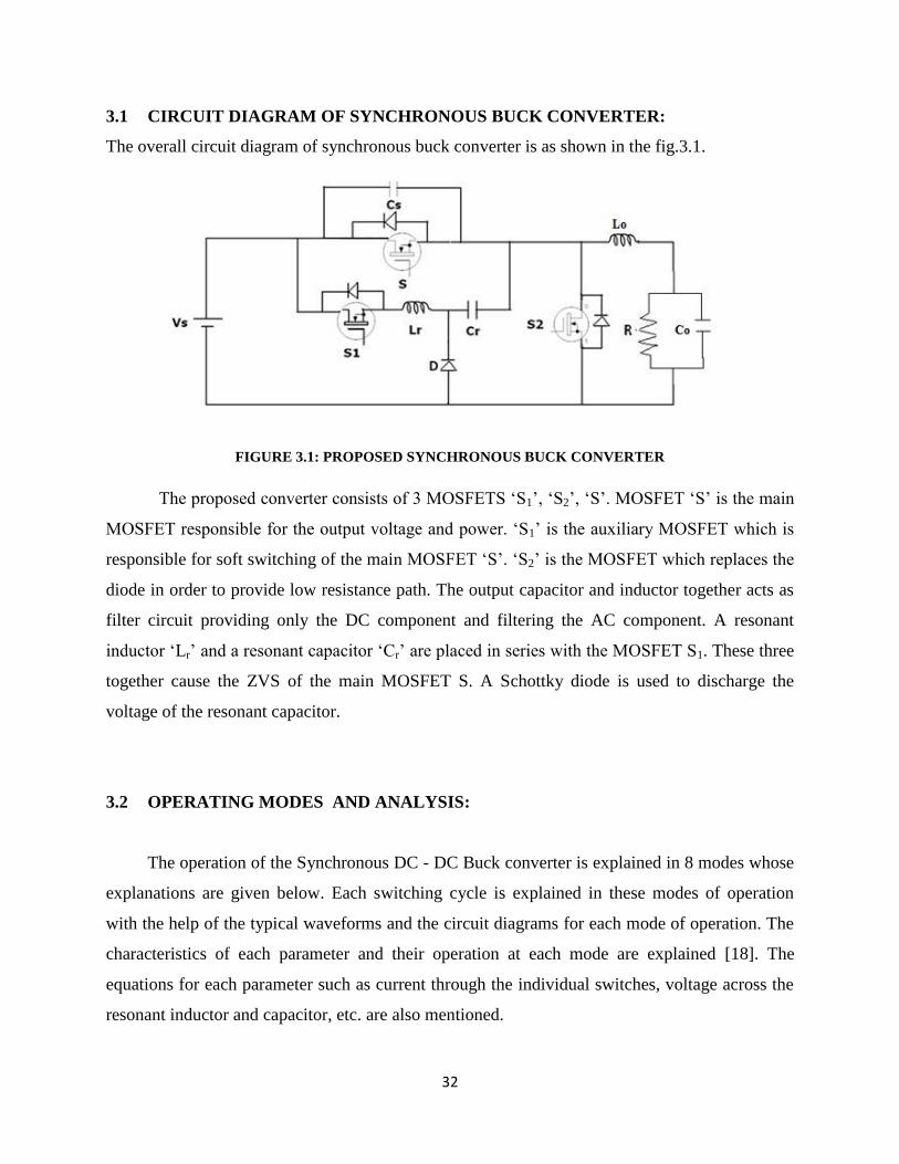
3.1 CIRCUIT DIAGRAM OF SYNCHRONOUS BUCK CONVERTER:
The overall circuit diagram of synchronous buck converter is as shown in the fig.3.1.
FIGURE 3.1: PROPOSED SYNCHRONOUS BUCK CONVERTER
The proposed converter consists of 3 MOSFETS „S1‟, „S2‟, „S‟. MOSFET „S‟ is the main
MOSFET responsible for the output voltage and power. „S1‟ is the auxiliary MOSFET which is
responsible for soft switching of the main MOSFET „S‟. „S2‟ is the MOSFET which replaces the
diode in order to provide low resistance path. The output capacitor and inductor together acts as
filter circuit providing only the DC component and filtering the AC component. A resonant
inductor „Lr‟ and a resonant capacitor „Cr‟ are placed in series with the MOSFET S1. These three
together cause the ZVS of the main MOSFET S. A Schottky diode is used to discharge the
voltage of the resonant capacitor.
3.2 OPERATING MODES AND ANALYSIS:
The operation of the Synchronous DC - DC Buck converter is explained in 8 modes whose
explanations are given below. Each switching cycle is explained in these modes of operation
with the help of the typical waveforms and the circuit diagrams for each mode of operation. The
characteristics of each parameter and their operation at each mode are explained [18]. The
equations for each parameter such as current through the individual switches, voltage across the
resonant inductor and capacitor, etc. are also mentioned.
33
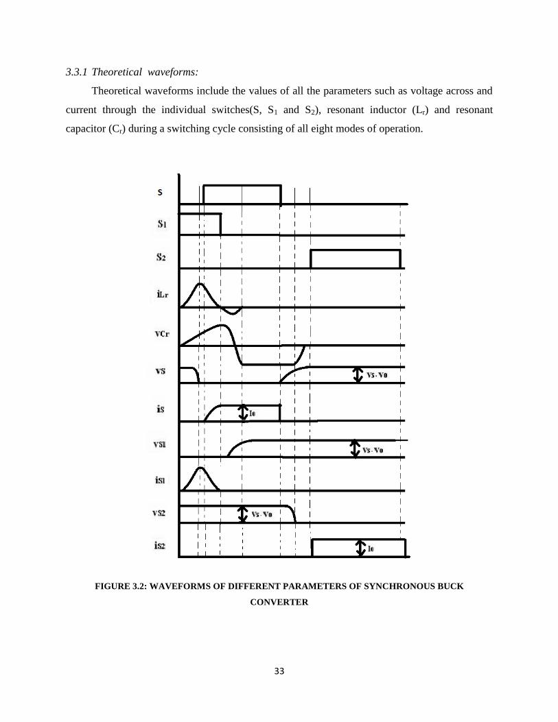
3.3.1 Theoretical waveforms:
Theoretical waveforms include the values of all the parameters such as voltage across and
current through the individual switches(S, S1 and S2), resonant inductor (Lr) and resonant
capacitor (Cr) during a switching cycle consisting of all eight modes of operation.
FIGURE 3.2: WAVEFORMS OF DIFFERENT PARAMETERS OF SYNCHRONOUS BUCK
CONVERTER
34
3.3.2 Modes of Operation:
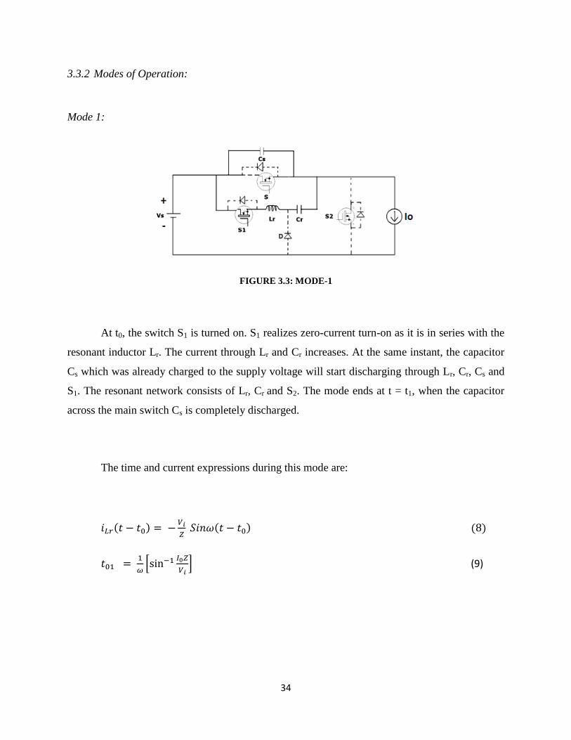
Mode 1:
FIGURE 3.3: MODE-1
At t0, the switch S1 is turned on. S1 realizes zero-current turn-on as it is in series with the
resonant inductor Lr. The current through Lr and Cr increases. At the same instant, the capacitor
Cs which was already charged to the supply voltage will start discharging through Lr, Cr, Cs and
S1. The resonant network consists of Lr, Cr and S2. The mode ends at t = t1, when the capacitor
across the main switch Cs is completely discharged.
The time and current expressions during this mode are:
(8)
*
+ (9)
35
Mode 2:
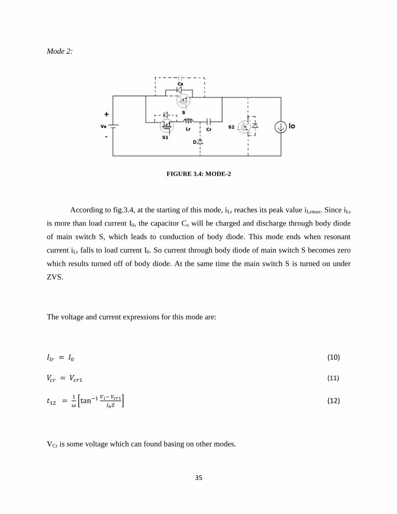
FIGURE 3.4: MODE-2
According to fig.3.4, at the starting of this mode, iLr reaches its peak value iLrmax. Since iLr
is more than load current I0, the capacitor Cs will be charged and discharge through body diode
of main switch S, which leads to conduction of body diode. This mode ends when resonant
current iLr falls to load current I0. So current through body diode of main switch S becomes zero
which results turned off of body diode. At the same time the main switch S is turned on under
ZVS.
The voltage and current expressions for this mode are:
(10)
(11)
*
+ (12)
VCr is some voltage which can found basing on other modes.
36
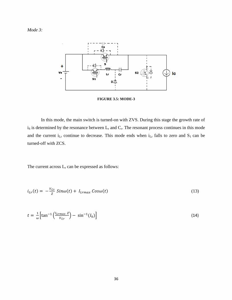
Mode 3:
FIGURE 3.5: MODE-3
In this mode, the main switch is turned-on with ZVS. During this stage the growth rate of
iS is determined by the resonance between Lr and Cr. The resonant process continues in this mode
and the current iLr continue to decrease. This mode ends when iLr falls to zero and S1 can be
turned-off with ZCS.
The current across Lr can be expressed as follows:
(13)
* (
) + (14)
37
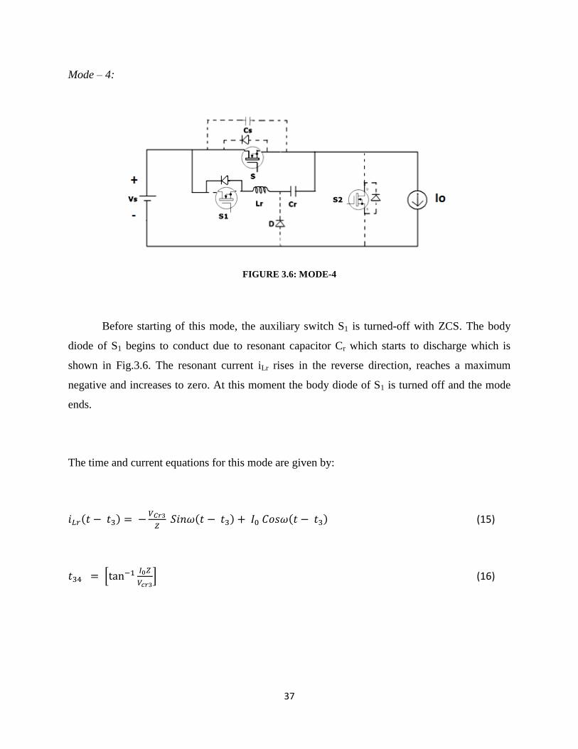
Mode – 4:
FIGURE 3.6: MODE-4
Before starting of this mode, the auxiliary switch S1 is turned-off with ZCS. The body
diode of S1 begins to conduct due to resonant capacitor Cr which starts to discharge which is
shown in Fig.3.6. The resonant current iLr rises in the reverse direction, reaches a maximum
negative and increases to zero. At this moment the body diode of S1 is turned off and the mode
ends.
The time and current equations for this mode are given by:
(15)
*
+ (16)
38
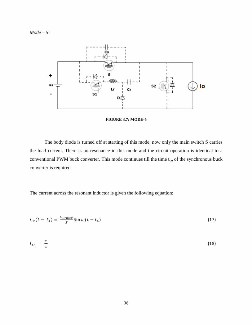
Mode – 5:
FIGURE 3.7: MODE-5
The body diode is turned off at starting of this mode, now only the main switch S carries
the load current. There is no resonance in this mode and the circuit operation is identical to a
conventional PWM buck converter. This mode continues till the time ton of the synchronous buck
converter is required.
The current across the resonant inductor is given the following equation:
(17)
(18)
39
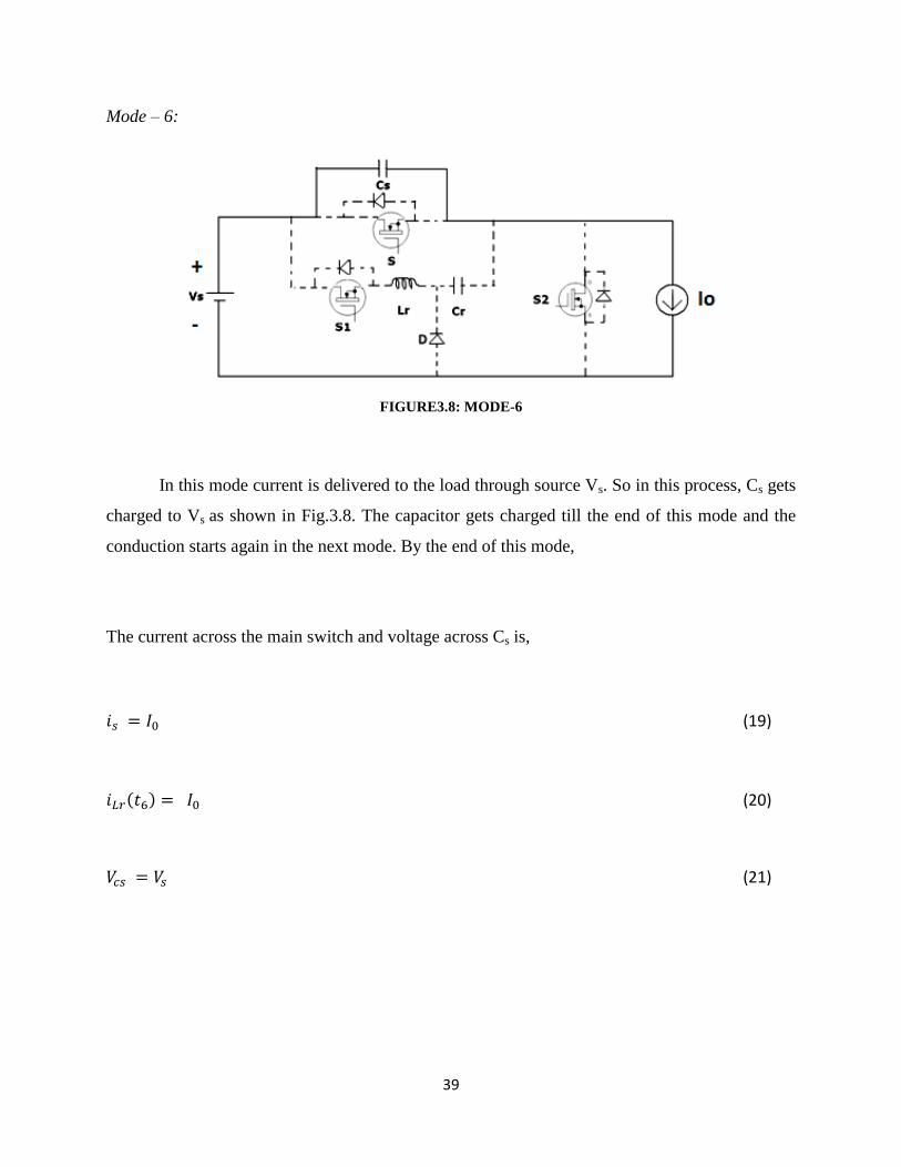
Mode – 6:
FIGURE3.8: MODE-6
In this mode current is delivered to the load through source Vs. So in this process, Cs gets
charged to Vs as shown in Fig.3.8. The capacitor gets charged till the end of this mode and the
conduction starts again in the next mode. By the end of this mode,
The current across the main switch and voltage across Cs is,
(19)
(20)
(21)

40
Mode – 7:
FIGURE 3.9: MODE-7
At starting of this mode, the main switch S is turned off with ZVS. The Schottky diode D
starts conducting. The resonant energy stored in the capacitor Cr starts discharging to the load
through the high frequency Schottky diode D for a very short period of time, hence body – diode
conduction losses and drop in output voltage is too low. This mode finishes when Cr is fully
discharged.
The voltage across Cr is given as follows:
(22)
41
Mode – 8:
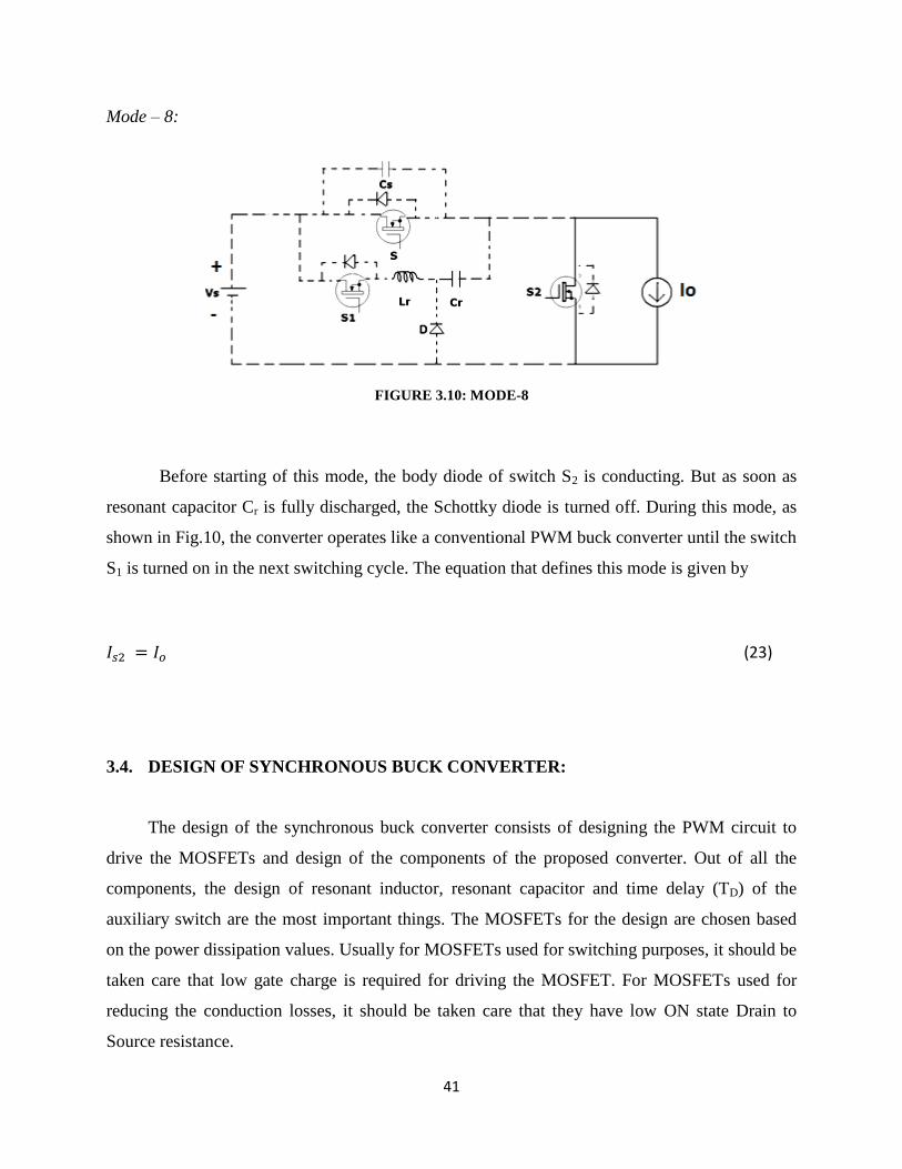
FIGURE 3.10: MODE-8
Before starting of this mode, the body diode of switch S2 is conducting. But as soon as
resonant capacitor Cr is fully discharged, the Schottky diode is turned off. During this mode, as
shown in Fig.10, the converter operates like a conventional PWM buck converter until the switch
S1 is turned on in the next switching cycle. The equation that defines this mode is given by
(23)
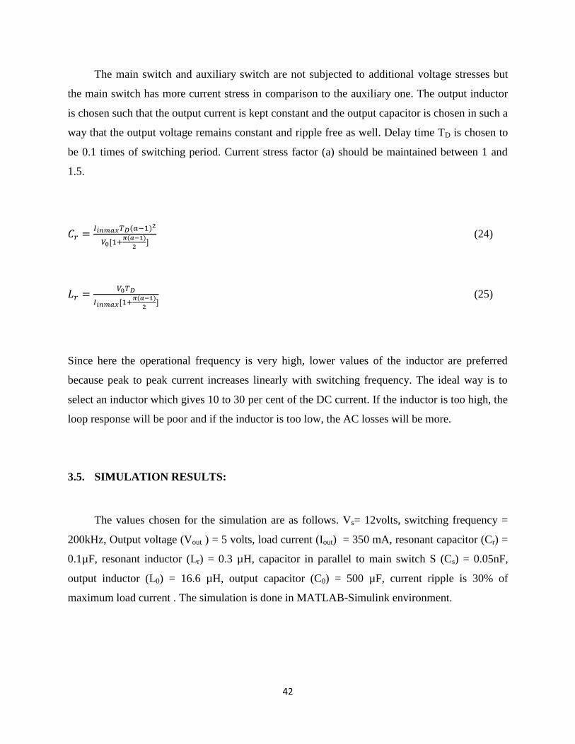
3.4. DESIGN OF SYNCHRONOUS BUCK CONVERTER:
The design of the synchronous buck converter consists of designing the PWM circuit to
drive the MOSFETs and design of the components of the proposed converter. Out of all the
components, the design of resonant inductor, resonant capacitor and time delay (TD) of the
auxiliary switch are the most important things. The MOSFETs for the design are chosen based
on the power dissipation values. Usually for MOSFETs used for switching purposes, it should be
taken care that low gate charge is required for driving the MOSFET. For MOSFETs used for
reducing the conduction losses, it should be taken care that they have low ON state Drain to
Source resistance.
42
The main switch and auxiliary switch are not subjected to additional voltage stresses but
the main switch has more current stress in comparison to the auxiliary one. The output inductor
is chosen such that the output current is kept constant and the output capacitor is chosen in such a
way that the output voltage remains constant and ripple free as well. Delay time TD is chosen to
be 0.1 times of switching period. Current stress factor (a) should be maintained between 1 and
1.5.
(24)
(25)
Since here the operational frequency is very high, lower values of the inductor are preferred
because peak to peak current increases linearly with switching frequency. The ideal way is to
select an inductor which gives 10 to 30 per cent of the DC current. If the inductor is too high, the
loop response will be poor and if the inductor is too low, the AC losses will be more.
3.5. SIMULATION RESULTS:
The values chosen for the simulation are as follows. Vs= 12volts, switching frequency =
200kHz, Output voltage (Vout ) = 5 volts, load current (Iout) = 350 mA, resonant capacitor (Cr) =
0.1µF, resonant inductor (Lr) = 0.3 µH, capacitor in parallel to main switch S (Cs) = 0.05nF,
output inductor (L0) = 16.6 µH, output capacitor (C0) = 500 µF, current ripple is 30% of
maximum load current . The simulation is done in MATLAB-Simulink environment.
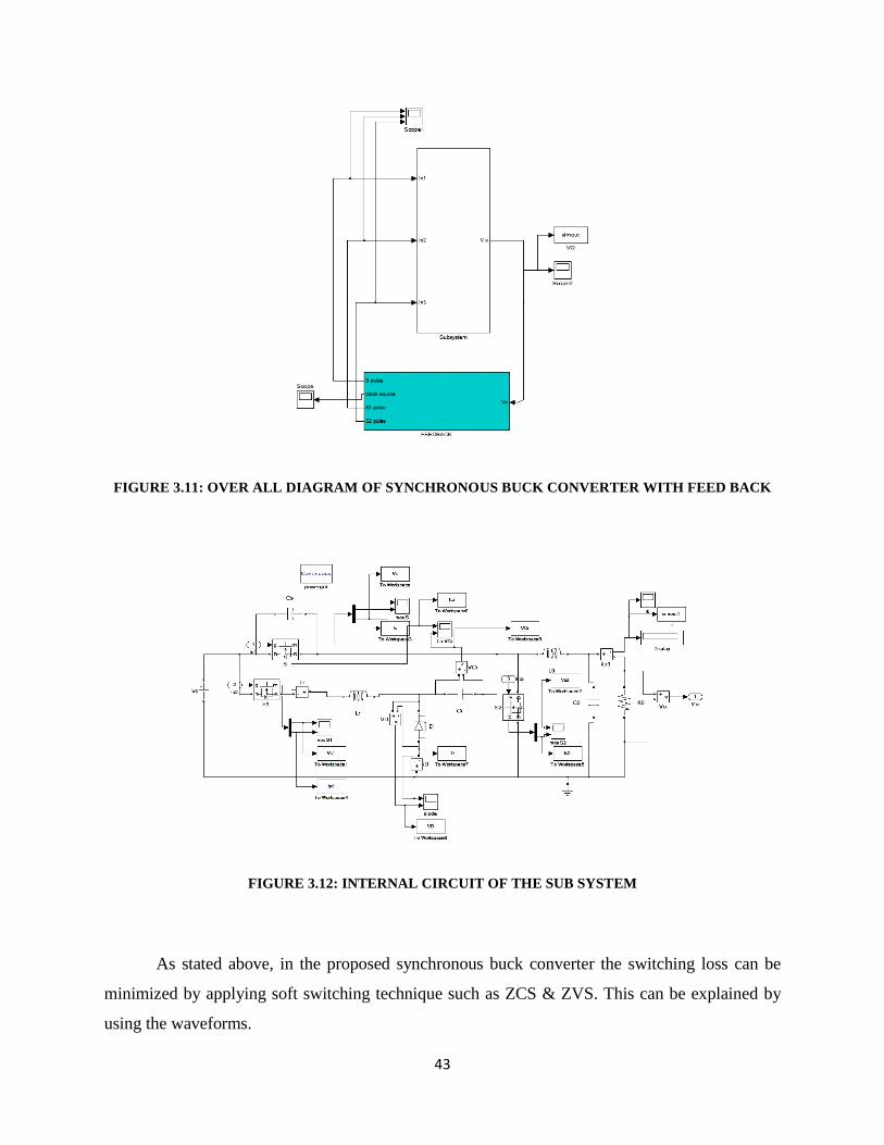
43
FIGURE 3.11: OVER ALL DIAGRAM OF SYNCHRONOUS BUCK CONVERTER WITH FEED BACK
FIGURE 3.12: INTERNAL CIRCUIT OF THE SUB SYSTEM
As stated above, in the proposed synchronous buck converter the switching loss can be
minimized by applying soft switching technique such as ZCS & ZVS. This can be explained by
using the waveforms.

44
FIGURE 3.13: RESPONSE OF CURRENT FLOWING THROUGH MOSFET ‘S’
FIGURE 3.14: RESPONSE OF VOLTAGE ACROSS MOSFET ‘S’
From the Fig. 3.13 and 3.14, it is clear that the MOSFET S is turned on through ZVS,
when the voltage across capacitor CS is zero. The voltage limit is not exceeded, but some current
stress is observed for a short period of time. The main switch is also turned off through ZVS.
0 10 20 30 40 50 600
2
4
6
8
10
12
14
Cu
rren
t ac
ross
MO
SF
ET
S i
n A
mp
s
time in micro seconds
waveform showing current v/s time across MOSFET S
0 50 100 1500
2
4
6
8
10
12
14
vo
ltag
e ac
ross
MO
SF
ET
S
time in micro seconds
waveform showing voltage v/s time for MOSFET S
45
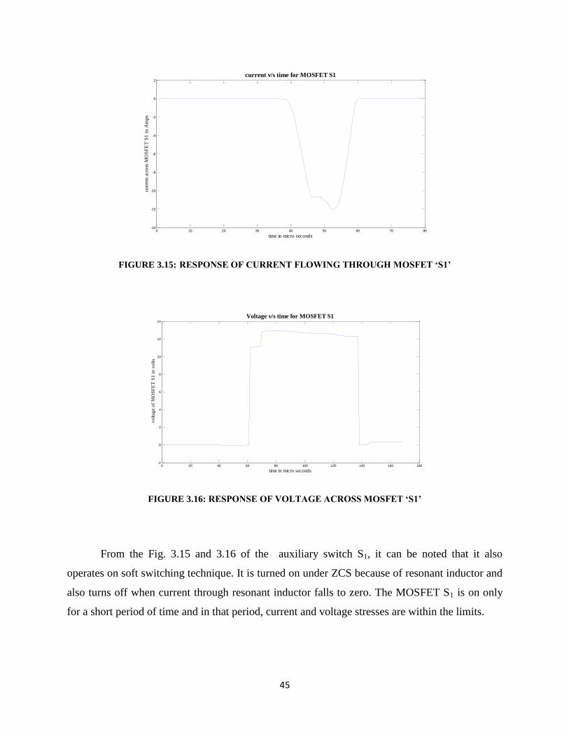
FIGURE 3.15: RESPONSE OF CURRENT FLOWING THROUGH MOSFET ‘S1’
FIGURE 3.16: RESPONSE OF VOLTAGE ACROSS MOSFET ‘S1’
From the Fig. 3.15 and 3.16 of the auxiliary switch S1, it can be noted that it also
operates on soft switching technique. It is turned on under ZCS because of resonant inductor and
also turns off when current through resonant inductor falls to zero. The MOSFET S1 is on only
for a short period of time and in that period, current and voltage stresses are within the limits.
0 10 20 30 40 50 60 70 80-14
-12
-10
-8
-6
-4
-2
0
2
curr
ent
acro
ss M
OS
FE
T S
1 i
n A
mp
s
time in micro seconds
current v/s time for MOSFET S1
0 20 40 60 80 100 120 140 160 180-2
0
2
4
6
8
10
12
14
Voltage v/s time for MOSFET S1
vo
ltag
e o
f M
OS
FE
T S
1 i
n v
olt
s
time in micro seconds
46
FIGURE 3.17: RESPONSE OF CURRENT FLOWING THROUGH MOSFET ‘S2’
FIGURE 3.18: RESPONSE OF VOLTAGE ACROSS MOSFET ‘S2’
The MOSFET S2 is turned on under ZVS when Cr is completely discharged and also
turns off under ZVS. The synchronous switch has characteristics similar to that of S and S1.
0 20 40 60 80 100 120 140 160 180-12
-10
-8
-6
-4
-2
0
time in micro seconds
curr
ent
acro
ss S
2 i
n A
mp
s
current across S2 v/s time
0 50 100 150-2
0
2
4
6
8
10
12
Vo
ltag
e ac
ross
S2
in
vo
lts
time in micro seconds
waveform showing voltage v/s time for MOSFET S2
47
FIGURE 3.19: RESPONSE OF VOLTAGE ACROSS SCHOTTKY DIODE
FIGURE 3.20: RESPONSE OF CURRENT FLOWING THROUGH SCHOTTKY DIODE
From the Fig. 3.19 and 3.20 of the Schottky diode, it is clear that the diode works for a
short period of time to discharge voltage across Cr. The Schottky diode is turned on and off
under ZVS. A high frequency Schottky diode with high current and low voltage capability is
used. The Schottky diode may cause some conduction loss because of which efficiency may
decrease and also output voltage may fall. But recently Schottky diodes with low conduction
losses are being introduced.
0 50 100 150-5
0
5
10
15
20
25
Vo
ltag
e ac
ross
dio
de
in v
olt
s
time in micro seconds
Diode voltage v/s time
0 50 100 150-2
0
2
4
6
8
10
time in micro seconds
Dio
de
curr
ent
in A
mp
s
Diode current v/s time
48
FIGURE 3.21: RESPONSE OF VOLTAGE ACROSS Cr
FIGURE 3.22: RESPONSE OF CURRENT FLOWING THROUGH ILr
3.6. CONCLUSION: Thus this section deals with the synchronous buck converter, its operating modes, design of
the components, simulation results. It can be seen that the simulation results are in accordance
with the theoretical waveforms. The waveforms depict the soft switching phenomena. This
converter is used as a DC-DC converter between PV array and load. Since the switching and
conduction losses are reduced, the system can be used as a high efficient portable device and also
the heat sink design is not required.
0 50 100 150-15
-10
-5
0
5
10
15
time in micro seconds
Vo
ltag
e ac
ross
Cr
in v
olt
s
VCr v/s time
0 20 40 60 80 100 120 140-2
0
2
4
6
8
10
12
14
curr
ent
acro
ss L
r in
Am
ps
time in micro seconds
ILr v/s time
49
CHAPTER 4
Practical Implementation of
Proposed Work Done
50
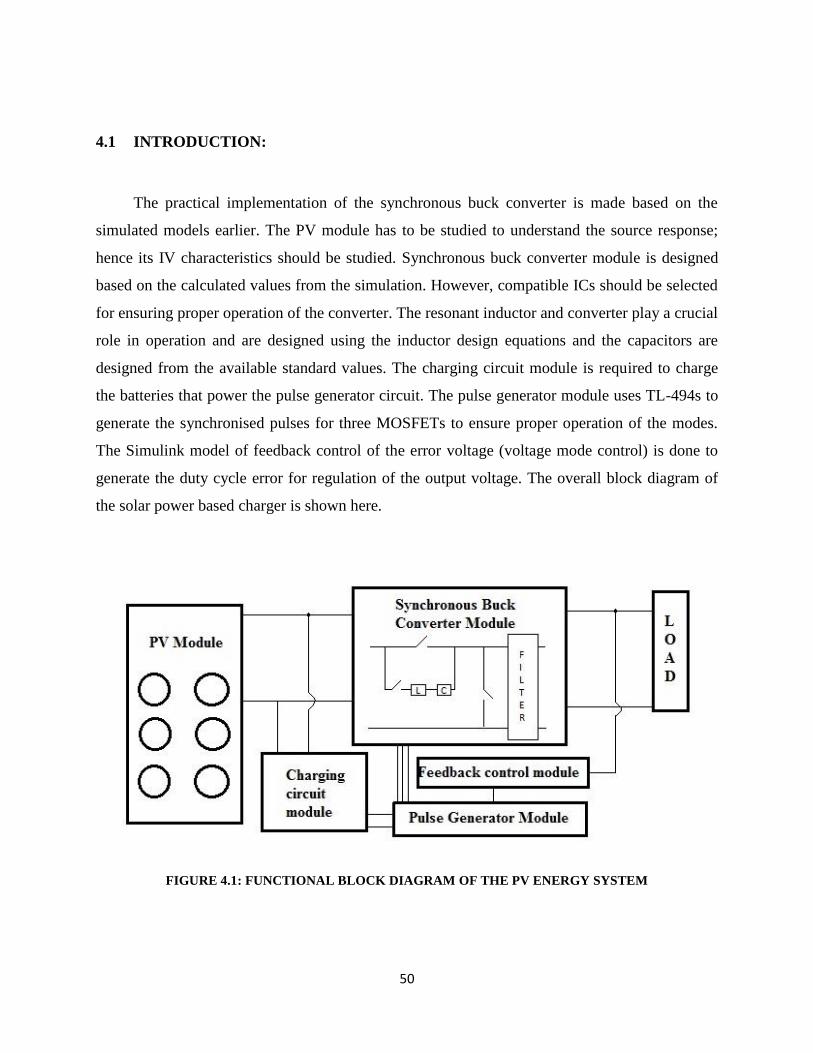
4.1 INTRODUCTION:
The practical implementation of the synchronous buck converter is made based on the
simulated models earlier. The PV module has to be studied to understand the source response;
hence its IV characteristics should be studied. Synchronous buck converter module is designed
based on the calculated values from the simulation. However, compatible ICs should be selected
for ensuring proper operation of the converter. The resonant inductor and converter play a crucial
role in operation and are designed using the inductor design equations and the capacitors are
designed from the available standard values. The charging circuit module is required to charge
the batteries that power the pulse generator circuit. The pulse generator module uses TL-494s to
generate the synchronised pulses for three MOSFETs to ensure proper operation of the modes.
The Simulink model of feedback control of the error voltage (voltage mode control) is done to
generate the duty cycle error for regulation of the output voltage. The overall block diagram of
the solar power based charger is shown here.
FIGURE 4.1: FUNCTIONAL BLOCK DIAGRAM OF THE PV ENERGY SYSTEM
51
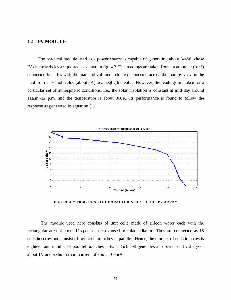
4.2 PV MODULE:
The practical module used as a power source is capable of generating about 3-4W whose
IV characteristics are plotted as shown in fig. 4.2. The readings are taken from an ammeter (for I)
connected in series with the load and voltmeter (for V) connected across the load by varying the
load from very high value (about 5K) to a negligible value. However, the readings are taken for a
particular set of atmospheric conditions, i.e., the solar insolation is constant at mid-day around
11a.m.-12 p.m. and the temperature is about 300K. Its performance is found to follow the
response as generated in equation (1).
FIGURE 4.2: PRACTICAL IV CHARACTERISTICS OF THE PV ARRAY
The module used here consists of unit cells made of silicon wafer each with the
rectangular area of about 11sq.cm that is exposed to solar radiation. They are connected as 18
cells in series and consist of two such branches in parallel. Hence, the number of cells in series is
eighteen and number of parallel branches is two. Each cell generates an open circuit voltage of
about 1V and a short circuit current of about 100mA.
52
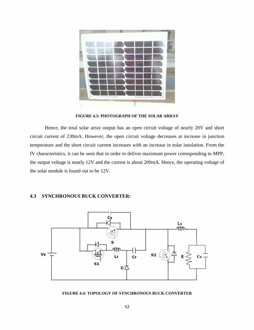
FIGURE 4.3: PHOTOGRAPH OF THE SOLAR ARRAY
Hence, the total solar array output has an open circuit voltage of nearly 20V and short
circuit current of 230mA. However, the open circuit voltage decreases at increase in junction
temperature and the short circuit current increases with an increase in solar insolation. From the
IV characteristics, it can be seen that in order to deliver maximum power corresponding to MPP,
the output voltage is nearly 12V and the current is about 200mA. Hence, the operating voltage of
the solar module is found out to be 12V.
4.3 SYNCHRONOUS BUCK CONVERTER:
FIGURE 4.4: TOPOLOGY OF SYNCHRONOUS BUCK CONVERTER
53
Synchronous Buck Converter Circuit consists of MOSFETs, inductor, capacitors, diode and
power supply. MOSFET used is IRF540N. It is a highly fast switching Integrated switch.
Inductor is coiled around a ferrite core. The circuit is as built such that getting the desired set of
switching pulse from the driving circuit; it steps down the voltage with lower switching loss by
using soft switching techniques as mentioned before. The diode (1N4007) in the conventional
buck converter is replaced with a Schottky diode as the forward voltage drop is less in the
Schottky diode and thus the power loss due to diode is also less. The input voltage to the
synchronous buck converter is 12 volts, and the desired output voltage and current is 3 volts and
500mA, which is attained by varying the duty cycle of switching pulse of switch S.
4.3.1 MOSFET (IRF540N):
MOSFET used in the synchronous buck converter is IRF540N. It is an N-channel
enhancement type power field effect transistor [18]. Three MOSFETs are used for each
switch S, S1 and S2. IRF540N is a highly fast switching Integrated circuit. As the MOSFET
can operate at high frequencies thus the output voltage is a steady DC voltage. The on- state
drain to source resistance is very low for this MOSFET. Thus, the power loss due to the drain
to source resistance is also very low. It also consists of an inherent body diode which helps in
the operation of MOSFET in the reverse direction also. This body diode also helps in the
operation of soft switching techniques in the synchronous buck converter.
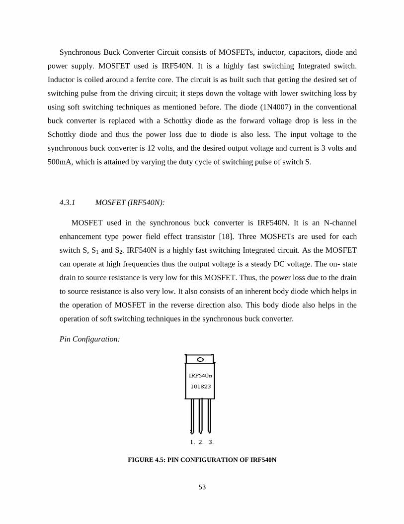
Pin Configuration:
FIGURE 4.5: PIN CONFIGURATION OF IRF540N
54
Pin -1 – Gate – In this pin the gate pulse is input to the MOSFET.
Pin -2 – Drain – In this pin the voltage VCC is supplied, which is positive with respect to the
source.
Pin -3 – Source – In this pin ground is connected through a load.
4.3.2 Capacitor Selection:
Two capacitors are used in the synchronous buck converter. Capacitor Cs of value is used
across the MOSFET S and the capacitor Cr is used in series with the inductor Lr. Cs is used to
close the MOSFET switch S with Zero Voltage switching (ZVS) and the capacitor Cr is used
to open the MOSFET switch S1 with zero current switching (ZCS). Ceramic capacitors are
used to get the desired value of capacitance and the circuit is completed as shown.
4.3.3 Schottky Diode (D) (1N5711):
Schottky Diode used in the synchronous buck converter discharges the resonant capacitor
Cr. This helps in the operation of Zero Voltage Switching of switch S2. The diode in the buck
converter is replaced by the Schottky diode [20] as the forward voltage drop during
conduction is less than that in the conventional Diode (1N4007). Thus the power loss due to
the diode is also very less and hence it enhances the efficiency. The low forward voltage drop
and fast switching makes it ideal for the circuit. The rated frequency of operation is 1 MHz
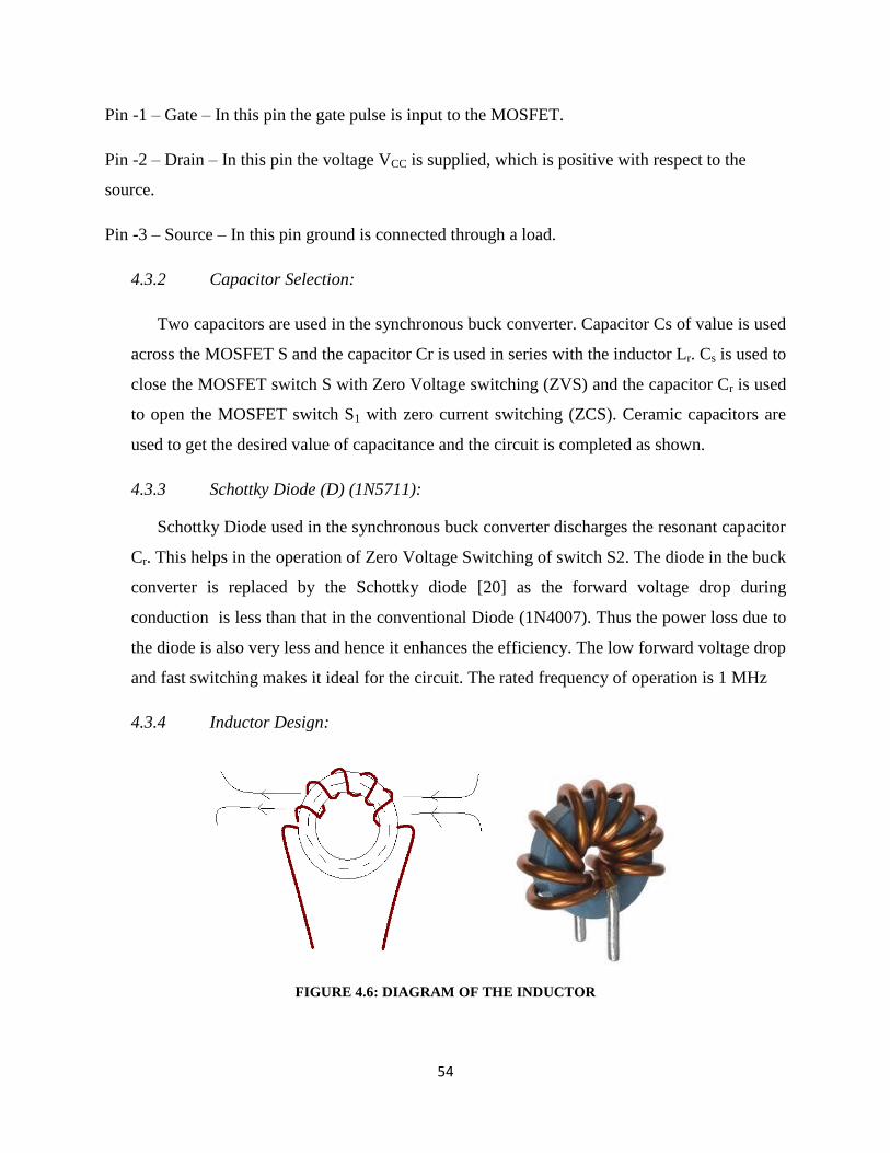
4.3.4 Inductor Design:
FIGURE 4.6: DIAGRAM OF THE INDUCTOR
55
Inductor of inductance 0.16 f is designed for the synchronous buck converter. The
inductor Lr with the help of capacitor Cr builds the resonance which helps in the operation of soft
switching techniques such as Zero Voltage Switching (ZVS) and Zero Current Switching (ZCS).
The on state resistance of the inductor causes a power loss which is relatively lower than other
losses. The inductor is designed using a ferrite core and coated copper windings [20].
The inductor of a specific value is designed by coiling coated copper windings across the
ferrite core. The inductance of a metallic core inductor depends on several factors such as
permeability of the material, number of turns, cross-section and the average length of the coil.
And this can be expressed in an equation as follows:
(26)
For the following parameters of the inductor,
The permeability of the core,
Number of the turns, N = 6
Average Coil Area, A = 0.00015 m2
Average length of the coil, l = 0.00001 m
The calculated value of Inductance of the inductor (in Henry) is:
56
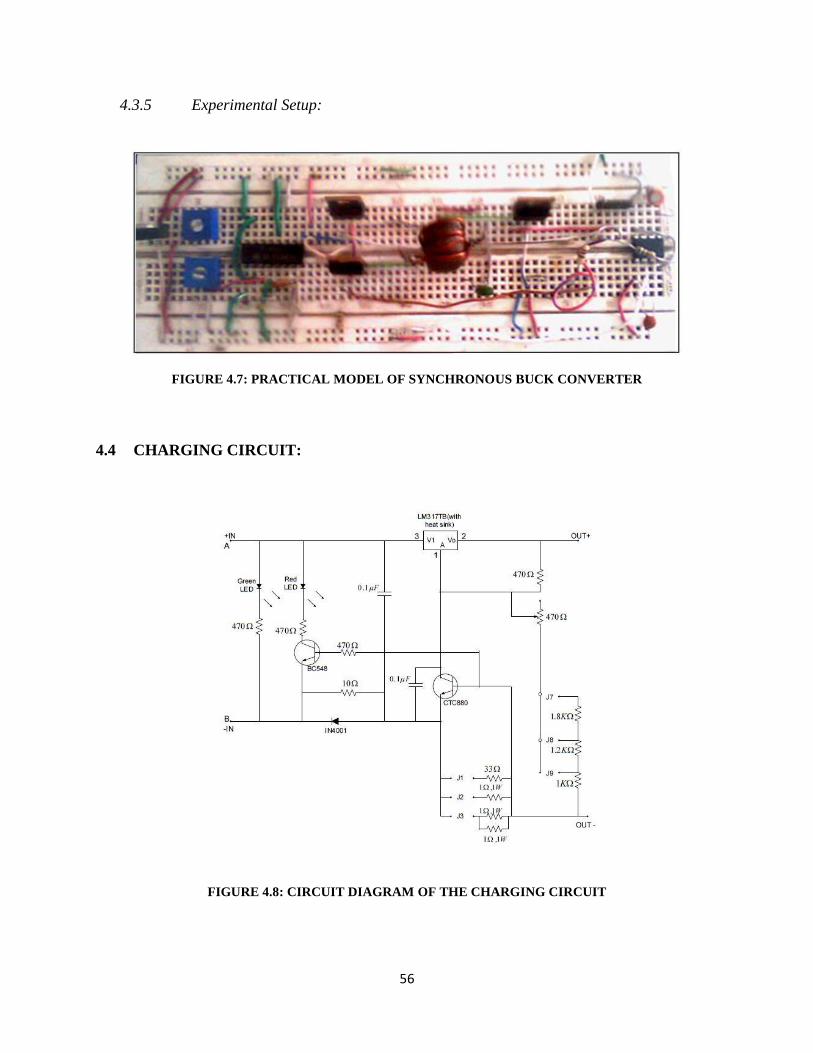
4.3.5 Experimental Setup:
FIGURE 4.7: PRACTICAL MODEL OF SYNCHRONOUS BUCK CONVERTER
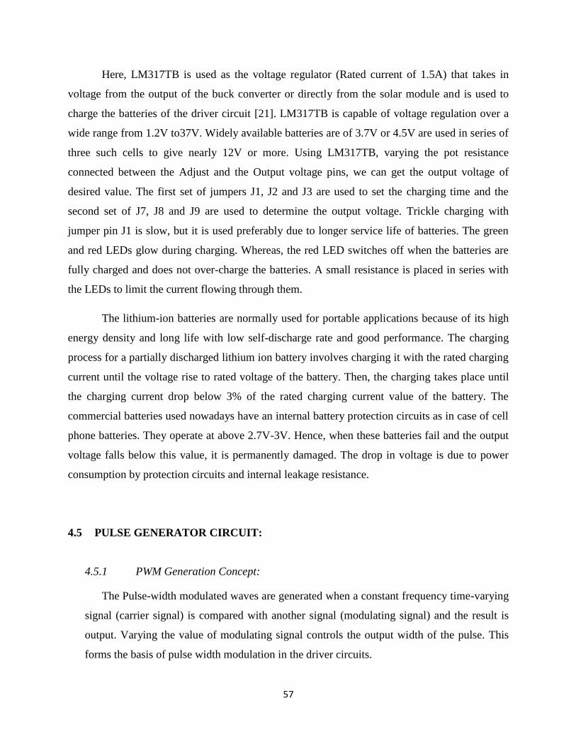
4.4 CHARGING CIRCUIT:
FIGURE 4.8: CIRCUIT DIAGRAM OF THE CHARGING CIRCUIT
57
Here, LM317TB is used as the voltage regulator (Rated current of 1.5A) that takes in
voltage from the output of the buck converter or directly from the solar module and is used to
charge the batteries of the driver circuit [21]. LM317TB is capable of voltage regulation over a
wide range from 1.2V to37V. Widely available batteries are of 3.7V or 4.5V are used in series of
three such cells to give nearly 12V or more. Using LM317TB, varying the pot resistance
connected between the Adjust and the Output voltage pins, we can get the output voltage of
desired value. The first set of jumpers J1, J2 and J3 are used to set the charging time and the
second set of J7, J8 and J9 are used to determine the output voltage. Trickle charging with
jumper pin J1 is slow, but it is used preferably due to longer service life of batteries. The green
and red LEDs glow during charging. Whereas, the red LED switches off when the batteries are
fully charged and does not over-charge the batteries. A small resistance is placed in series with
the LEDs to limit the current flowing through them.
The lithium-ion batteries are normally used for portable applications because of its high
energy density and long life with low self-discharge rate and good performance. The charging
process for a partially discharged lithium ion battery involves charging it with the rated charging
current until the voltage rise to rated voltage of the battery. Then, the charging takes place until
the charging current drop below 3% of the rated charging current value of the battery. The
commercial batteries used nowadays have an internal battery protection circuits as in case of cell
phone batteries. They operate at above 2.7V-3V. Hence, when these batteries fail and the output
voltage falls below this value, it is permanently damaged. The drop in voltage is due to power
consumption by protection circuits and internal leakage resistance.
4.5 PULSE GENERATOR CIRCUIT:
4.5.1 PWM Generation Concept:
The Pulse-width modulated waves are generated when a constant frequency time-varying
signal (carrier signal) is compared with another signal (modulating signal) and the result is
output. Varying the value of modulating signal controls the output width of the pulse. This
forms the basis of pulse width modulation in the driver circuits.
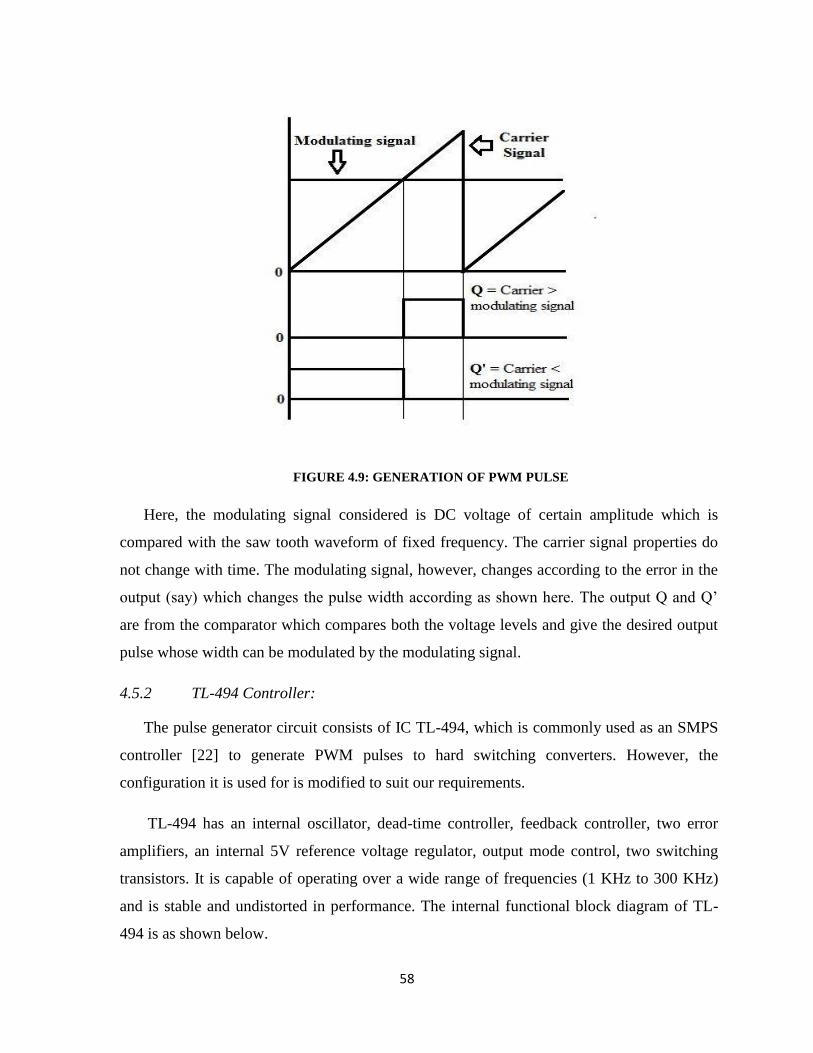
58
FIGURE 4.9: GENERATION OF PWM PULSE
Here, the modulating signal considered is DC voltage of certain amplitude which is
compared with the saw tooth waveform of fixed frequency. The carrier signal properties do
not change with time. The modulating signal, however, changes according to the error in the
output (say) which changes the pulse width according as shown here. The output Q and Q‟
are from the comparator which compares both the voltage levels and give the desired output
pulse whose width can be modulated by the modulating signal.
4.5.2 TL-494 Controller:
The pulse generator circuit consists of IC TL-494, which is commonly used as an SMPS
controller [22] to generate PWM pulses to hard switching converters. However, the
configuration it is used for is modified to suit our requirements.
TL-494 has an internal oscillator, dead-time controller, feedback controller, two error
amplifiers, an internal 5V reference voltage regulator, output mode control, two switching
transistors. It is capable of operating over a wide range of frequencies (1 KHz to 300 KHz)
and is stable and undistorted in performance. The internal functional block diagram of TL-
494 is as shown below.
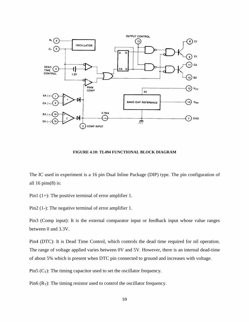
59
FIGURE 4.10: TL494 FUNCTIONAL BLOCK DIAGRAM
The IC used in experiment is a 16 pin Dual Inline Package (DIP) type. The pin configuration of
all 16 pins(8) is:
Pin1 (1+): The positive terminal of error amplifier 1.
Pin2 (1-): The negative terminal of error amplifier 1.
Pin3 (Comp input): It is the external comparator input or feedback input whose value ranges
between 0 and 3.3V.
Pin4 (DTC): It is Dead Time Control, which controls the dead time required for nil operation.
The range of voltage applied varies between 0V and 5V. However, there is an internal dead-time
of about 5% which is present when DTC pin connected to ground and increases with voltage.
Pin5 (CT): The timing capacitor used to set the oscillator frequency.
Pin6 (RT): The timing resistor used to control the oscillator frequency.

60
Pin7 (GND): The common ground of TL-494 that is connected to the source ground terminal.
Pin8 (C1): The collector terminal of switching transistor 1.
Pin9 (E1): The emitter terminal of switching transistor 1.
Pin10 (E2): The emitter terminal of switching transistor 2.
Pin11 (C2): The collector terminal of switching transistor 2.
Pin12 (VCC): The positive voltage supply to power the IC.
Pin13 (Output control): The mode of output from the two switching transistors 1 and 2 is
controlled by setting high or low value at this input. When it is grounded, the transistors operate
in parallel. When it is set high to VREF, the transistors operate in push-pull fashion.
Pin14 (VREF): The output of 5V used for comparators is taken from this pin which is connected
internally to 5V internal voltage regulator.
Pin15 (2-): The negative terminal of error amplifier 2.
Pin16 (2+): The positive terminal of error amplifier 2.
The configuration used to generate a single PWM pulse from TL-494 is as follows.
The frequency of operation of TL494 is given by
. For 200 KHz operation, the values chosen
for RT and CT are 5K and 1KpF respectively. There are two different configurations possible for
getting a PWM pulse. One is control over rising edge and the other is control over falling edge of
the pulse.
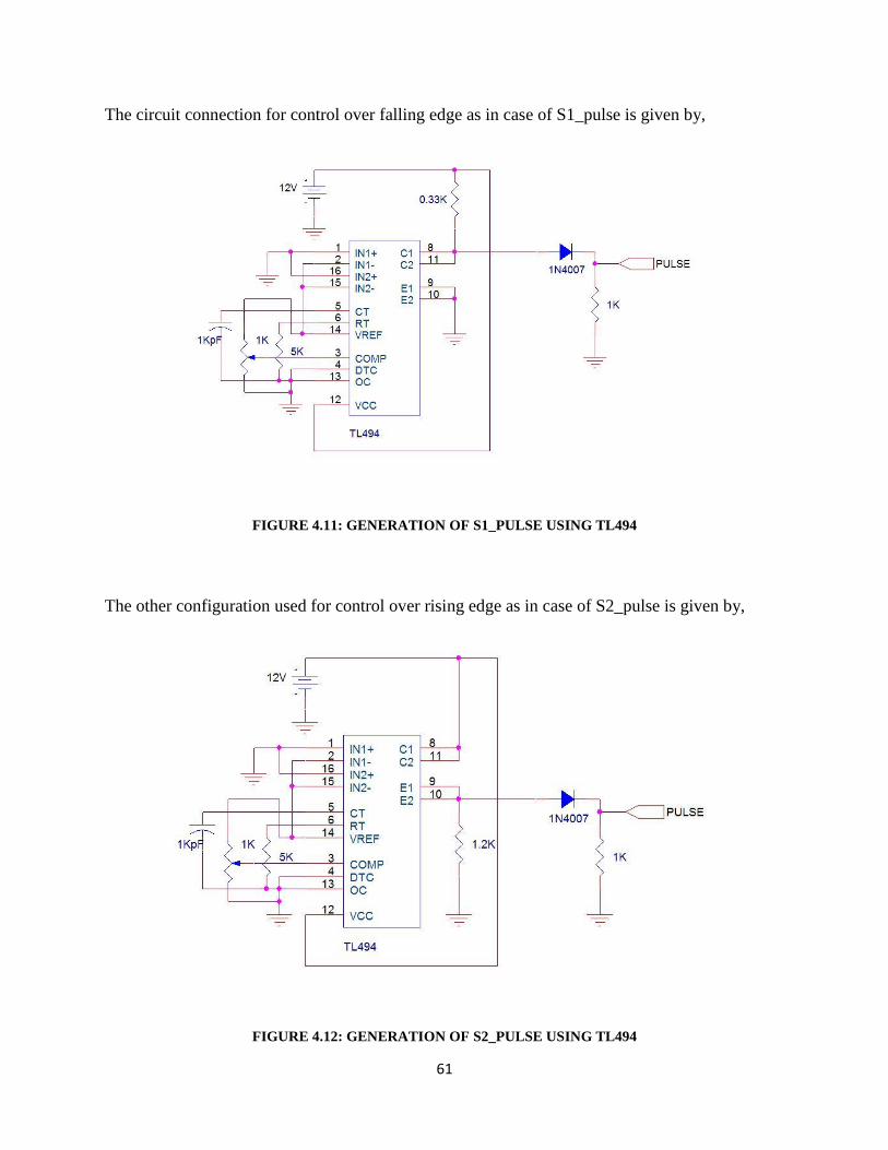
61
The circuit connection for control over falling edge as in case of S1_pulse is given by,
FIGURE 4.11: GENERATION OF S1_PULSE USING TL494
The other configuration used for control over rising edge as in case of S2_pulse is given by,
FIGURE 4.12: GENERATION OF S2_PULSE USING TL494
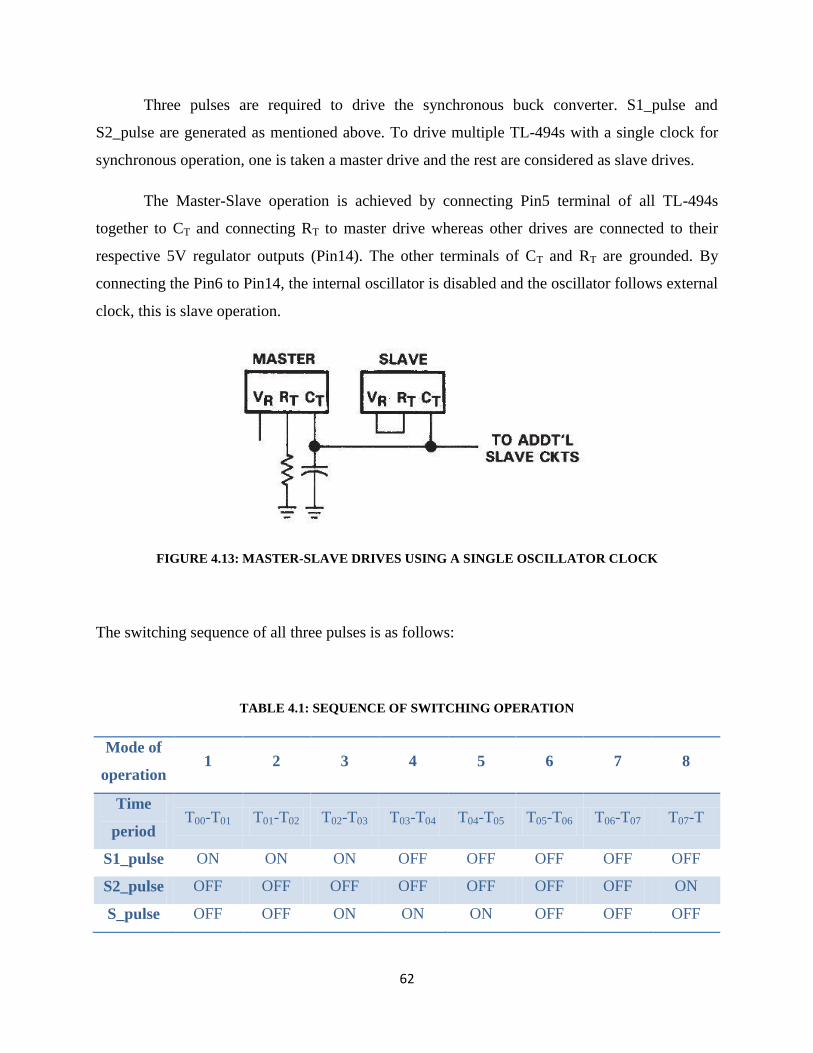
62
Three pulses are required to drive the synchronous buck converter. S1_pulse and
S2_pulse are generated as mentioned above. To drive multiple TL-494s with a single clock for
synchronous operation, one is taken a master drive and the rest are considered as slave drives.
The Master-Slave operation is achieved by connecting Pin5 terminal of all TL-494s
together to CT and connecting RT to master drive whereas other drives are connected to their
respective 5V regulator outputs (Pin14). The other terminals of CT and RT are grounded. By
connecting the Pin6 to Pin14, the internal oscillator is disabled and the oscillator follows external
clock, this is slave operation.
FIGURE 4.13: MASTER-SLAVE DRIVES USING A SINGLE OSCILLATOR CLOCK
The switching sequence of all three pulses is as follows:
TABLE 4.1: SEQUENCE OF SWITCHING OPERATION
Mode of
operation 1 2 3 4 5 6 7 8
Time
period T00-T01 T01-T02 T02-T03 T03-T04 T04-T05 T05-T06 T06-T07 T07-T
S1_pulse ON ON ON OFF OFF OFF OFF OFF
S2_pulse OFF OFF OFF OFF OFF OFF OFF ON
S_pulse OFF OFF ON ON ON OFF OFF OFF
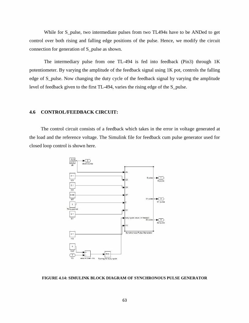
63
While for S_pulse, two intermediate pulses from two TL494s have to be ANDed to get
control over both rising and falling edge positions of the pulse. Hence, we modify the circuit
connection for generation of S_pulse as shown.
The intermediary pulse from one TL-494 is fed into feedback (Pin3) through 1K
potentiometer. By varying the amplitude of the feedback signal using 1K pot, controls the falling
edge of S_pulse. Now changing the duty cycle of the feedback signal by varying the amplitude
level of feedback given to the first TL-494, varies the rising edge of the S_pulse.
4.6 CONTROL/FEEDBACK CIRCUIT:
The control circuit consists of a feedback which takes in the error in voltage generated at
the load and the reference voltage. The Simulink file for feedback cum pulse generator used for
closed loop control is shown here.
FIGURE 4.14: SIMULINK BLOCK DIAGRAM OF SYNCHRONOUS PULSE GENERATOR
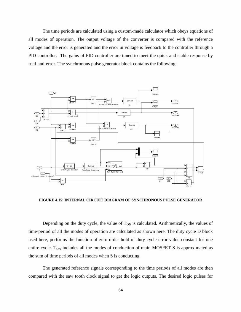
64
The time periods are calculated using a custom-made calculator which obeys equations of
all modes of operation. The output voltage of the converter is compared with the reference
voltage and the error is generated and the error in voltage is feedback to the controller through a
PID controller. The gains of PID controller are tuned to meet the quick and stable response by
trial-and-error. The synchronous pulse generator block contains the following:
FIGURE 4.15: INTERNAL CIRCUIT DIAGRAM OF SYNCHRONOUS PULSE GENERATOR
Depending on the duty cycle, the value of TON is calculated. Arithmetically, the values of
time-period of all the modes of operation are calculated as shown here. The duty cycle D block
used here, performs the function of zero order hold of duty cycle error value constant for one
entire cycle. TON includes all the modes of conduction of main MOSFET S is approximated as
the sum of time periods of all modes when S is conducting.
The generated reference signals corresponding to the time periods of all modes are then
compared with the saw tooth clock signal to get the logic outputs. The desired logic pulses for
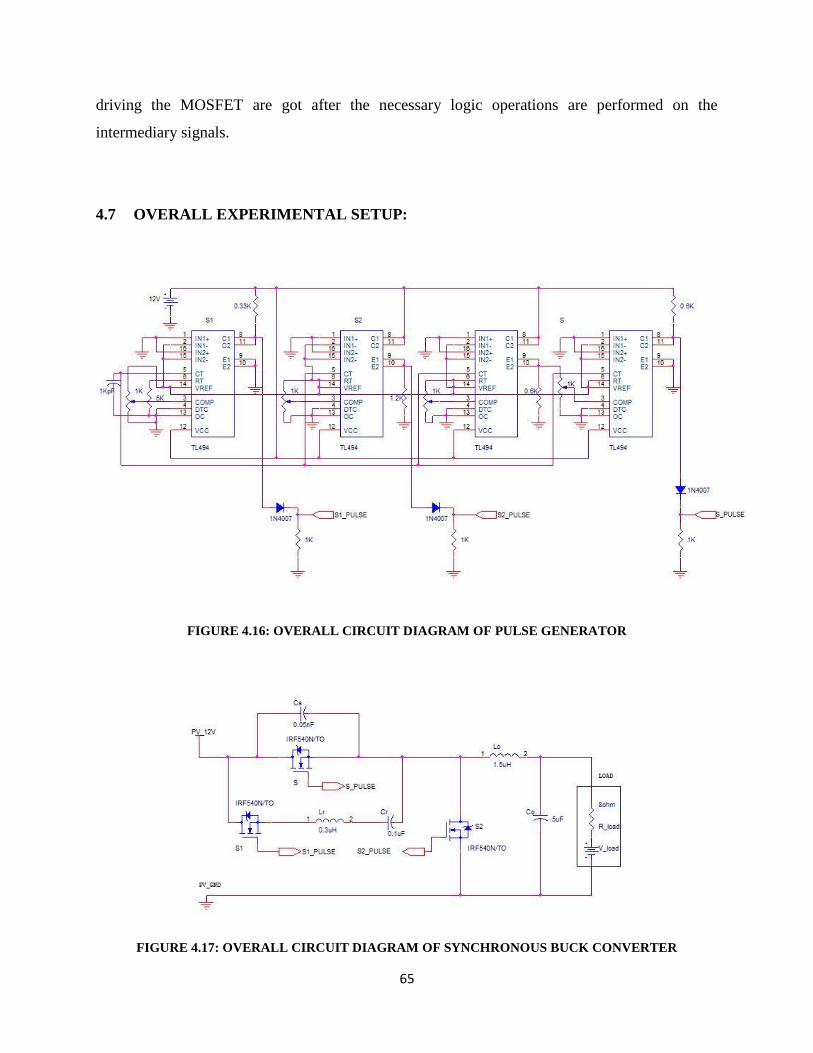
65
driving the MOSFET are got after the necessary logic operations are performed on the
intermediary signals.
4.7 OVERALL EXPERIMENTAL SETUP:
FIGURE 4.16: OVERALL CIRCUIT DIAGRAM OF PULSE GENERATOR
FIGURE 4.17: OVERALL CIRCUIT DIAGRAM OF SYNCHRONOUS BUCK CONVERTER
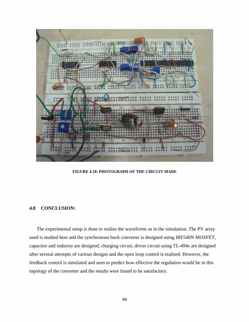
66
FIGURE 4.18: PHOTOGRAPH OF THE CIRCUIT MADE
4.8 CONCLUSION:
The experimental setup is done to realise the waveforms as in the simulation. The PV array
used is studied here and the synchronous buck converter is designed using IRF540N MOSFET,
capacitor and inductor are designed, charging circuit, driver circuit using TL-494s are designed
after several attempts of various designs and the open loop control is realised. However, the
feedback control is simulated and seen to predict how effective the regulation would be in this
topology of the converter and the results were found to be satisfactory.
67
CHAPTER 5
Experimental Results and
Comparative Study
68
5.1 INTRODUCTION:
Experimental results are the most important part as it helps to validate the model of a
project with the simulation results. It also ensures the proper working of the model. It helps to
have a comparative study among different converter topologies.
In this chapter, the experiment results of the conventional buck converter have been
provided. It also includes the voltage pulse output of the driving circuit. The Digital Signal
Oscilloscope output includes the saw tooth voltage waveform and the pulse for driving gate of
each of the MOSFET switches. The Solar irradiation and temperature and Photo voltaic array
voltage, current values are noted against time. The mentioned notification are plotted and
presented. It helps us to determine the characteristics of the photovoltaic with respect to the solar
temperature and solar irradiation. At last, a comparative study between the conventional buck
converter and synchronous buck converter is presented. This comparative study also determines
the overall efficiency of the conventional buck converter and the synchronous buck converter. It
helps to compare between the buck converter and the synchronous buck converter.
FIGURE 5.1: COMPLETE EXPERIMENTAL SETUP FOR PROPOSED WORK DONE
69
5.2 EXPERIMENTAL RESULTS:
FIGURE 5.2: COMPARISON OF SAW TOOTH AND CONTROL VOLTAGE
The fig. 5.2 shows the pulse generation phenomenon. The reference signal is compared
with the saw tooth input and gate pulse is generated.
FIGURE 5.3: GATE PULSE FOR MOSFET S1
The gate pulse S1 is produced by comparing the clock with a reference signal, to generate
the ON for a time t02, which can be seen in fig. 5.3.
70
FIGURE 5.4: GATE PULSE FOR MOSFET S2
As it can be seen from the fig.5.4, the gate pulse for MOSFET S2 is obtained by
comparing the reference signal with the clock signal, to generate the pulse for time period t7-t8.
FIGURE 5.5: GATE PULSE FOR MOSFET S
Fig. 5.5 shows the resultant output gate pulse for MOSFET S. The Main Switch „S‟ is ON during
the period t2-t5. This is achieved by AND operation on two intermediary pulses, each of which
controls a rising and a falling edge of the pulse. It can be seen here that S pulse is OFF during t02.
Also, the pulse is off during t5-t8. In the remaining time, it is ON. For open loop control, it can
also be generated by feeding back the intermediary signal from one comparator into the feedback
input of the other comparator through a potentiometer.
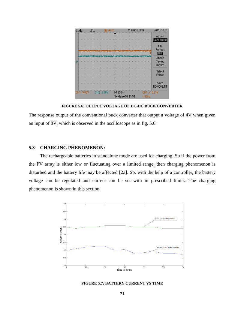
71
FIGURE 5.6: OUTPUT VOLTAGE OF DC-DC BUCK CONVERTER
The response output of the conventional buck converter that output a voltage of 4V when given
an input of 8V, which is observed in the oscilloscope as in fig. 5.6.
5.3 CHARGING PHENOMENON:
The rechargeable batteries in standalone mode are used for charging. So if the power from
the PV array is either low or fluctuating over a limited range, then charging phenomenon is
disturbed and the battery life may be affected [23]. So, with the help of a controller, the battery
voltage can be regulated and current can be set with in prescribed limits. The charging
phenomenon is shown in this section.
FIGURE 5.7: BATTERY CURRENT VS TIME
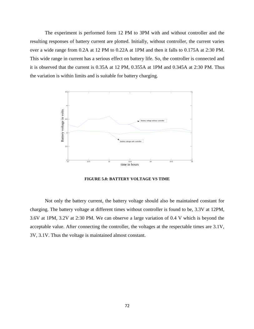
72
The experiment is performed form 12 PM to 3PM with and without controller and the
resulting responses of battery current are plotted. Initially, without controller, the current varies
over a wide range from 0.2A at 12 PM to 0.22A at 1PM and then it falls to 0.175A at 2:30 PM.
This wide range in current has a serious effect on battery life. So, the controller is connected and
it is observed that the current is 0.35A at 12 PM, 0.355A at 1PM and 0.345A at 2:30 PM. Thus
the variation is within limits and is suitable for battery charging.
FIGURE 5.8: BATTERY VOLTAGE VS TIME
Not only the battery current, the battery voltage should also be maintained constant for
charging. The battery voltage at different times without controller is found to be, 3.3V at 12PM,
3.6V at 1PM, 3.2V at 2:30 PM. We can observe a large variation of 0.4 V which is beyond the
acceptable value. After connecting the controller, the voltages at the respectable times are 3.1V,
3V, 3.1V. Thus the voltage is maintained almost constant.
12 12.5 13 13.5 14 14.5 152
2.5
3
3.5
4
4.5
time in hours
Bat
tery
vo
ltag
e in
vo
lts
Battery voltage without controller
Battery voltage with controller
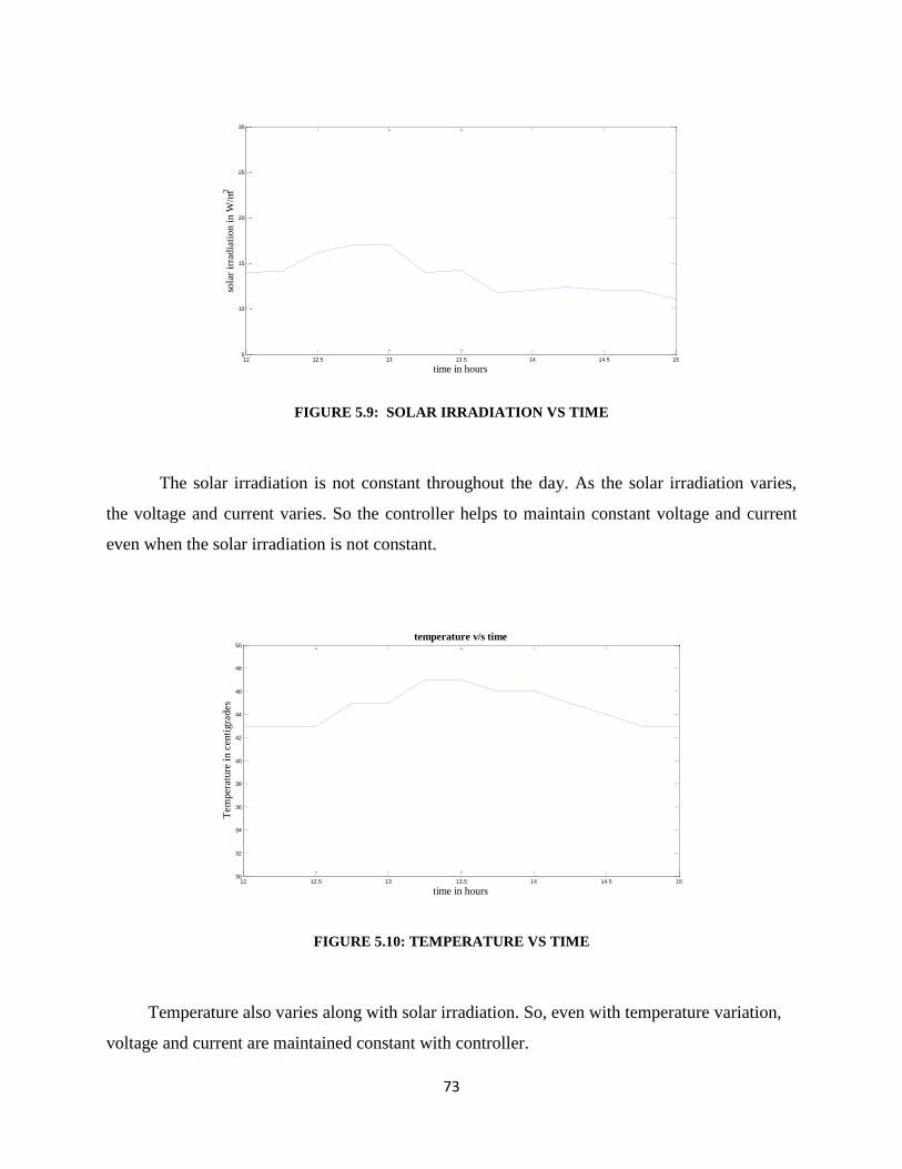
73
FIGURE 5.9: SOLAR IRRADIATION VS TIME
The solar irradiation is not constant throughout the day. As the solar irradiation varies,
the voltage and current varies. So the controller helps to maintain constant voltage and current
even when the solar irradiation is not constant.
FIGURE 5.10: TEMPERATURE VS TIME
Temperature also varies along with solar irradiation. So, even with temperature variation,
voltage and current are maintained constant with controller.
12 12.5 13 13.5 14 14.5 155
10
15
20
25
30
sola
r ir
rad
iati
on
in
W/m
2
time in hours
12 12.5 13 13.5 14 14.5 1530
32
34
36
38
40
42
44
46
48
50
time in hours
Tem
pera
ture
in c
enti
gra
des
temperature v/s time
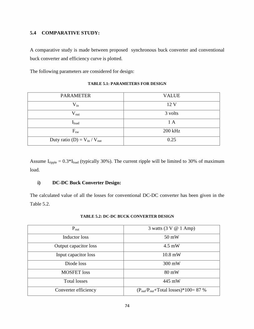
74
5.4 COMPARATIVE STUDY:
A comparative study is made between proposed synchronous buck converter and conventional
buck converter and efficiency curve is plotted.
The following parameters are considered for design:
TABLE 5.1: PARAMETERS FOR DESIGN
PARAMETER VALUE
Vin 12 V
Vout 3 volts
Iload 1 A
Fsw 200 kHz
Duty ratio (D) = Vin / Vout 0.25
Assume Iripple = 0.3*Iload (typically 30%). The current ripple will be limited to 30% of maximum
load.
i) DC-DC Buck Converter Design:
The calculated value of all the losses for conventional DC-DC converter has been given in the
Table 5.2.
TABLE 5.2: DC-DC BUCK CONVERTER DESIGN
Pout 3 watts (3 V @ 1 Amp)
Inductor loss 50 mW
Output capacitor loss 4.5 mW
Input capacitor loss 10.8 mW
Diode loss 300 mW
MOSFET loss 80 mW
Total losses 445 mW
Converter efficiency (Pout/Pout+Total losses)*100= 87 %
75
Here 60 % of total losses are mainly due to diode forward voltage drop (0.4 V).The converter
efficiency can be raised if the diode‟s forward voltage drop will be lowered. The overall design
of DC-DC buck converter will be shown in Appendix (a).
ii) Synchronous Buck Converter Design:
For the same design parameters, the calculated values of all the losses have been tabulated in 5.3.
TABLE 5.3: PROPOSED SYNCHRONOUS BUCK CONVERTER DESIGN
Pout 3 watts (3 V @ 1 A)
N-channel MOSFET with Rds (on) 0.0044 Ώ
Conduction loss Id2*Rds (on)*(1-D) = 15 mW
Main MOSFET (S) loss 10 mW
Resonant capacitor (Cr) loss 10 mW
Resonant Inductor (Lr) loss 50 mW
Output capacitor loss (Co) 4.5 mW
MOSFET (S1+S2) loss 75 mW
Diode (D) loss 5 mW
Output Inductor (L0) loss 20 mW
Total Losses 190 mW
Converter efficiency (3/3+0.190)*100= 94 %
From the above design consideration of both conventional buck and synchronous buck
converter, we found that the efficiency of synchronous buck converter is more than that of
conventional buck converter for same output power rating. The relevant graphical representation
is shown in fig 5.11.
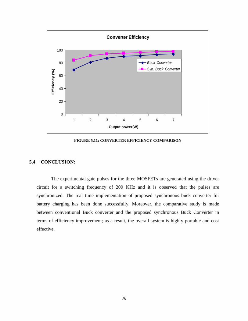
76
FIGURE 5.11: CONVERTER EFFICIENCY COMPARISON
5.4 CONCLUSION:
The experimental gate pulses for the three MOSFETs are generated using the driver
circuit for a switching frequency of 200 KHz and it is observed that the pulses are
synchronized. The real time implementation of proposed synchronous buck converter for
battery charging has been done successfully. Moreover, the comparative study is made
between conventional Buck converter and the proposed synchronous Buck Converter in
terms of efficiency improvement; as a result, the overall system is highly portable and cost
effective.
Converter Efficiency
0
20
40
60
80
100
1 2 3 4 5 6 7
Output power(W)
Eff
icie
ncy (
%)
Buck Converter
Syn. Buck Converter
77
CHAPTER 6
Conclusion and Future work
78
6.1 CONCLUSION:
The PV energy systems that are available in the market are known and the feasibility of
portable charging systems is analysed. The PV array model is simulated and check with the
practical model to check its characteristics. The high efficiency synchronous buck converter
is studied and is simulated in MATLAB-Simulink environment with PV array to know the
characteristics of the converter. Further, the real time implementation of proposed
synchronous buck converter for battery charging has been done successfully. Moreover, the
comparative study is made between conventional Buck converter and the proposed
synchronous Buck Converter in terms of efficiency improvement; as a result, the overall
system is highly portable and cost effective.
6.2 FUTURE WORK:
The converter designed in this project operates at 200 KHz. However, for faster
response at higher frequencies with easily customisable control, FPGA implementation can
be made and can be integrated with micro controller control for more stability in output at
various conditions. Such low cost systems with less error due to digital operation can be used
to operate low power high current devices and also the isolated house power can be managed
with these microcontroller based systems which has an added advantage of flexibility and
ability to interact with other devices. Thus the freedom to get electricity anywhere and the
adaptability of micro controllers to suit many conditions easily can be exploited to make such
portable systems in an effective and user-friendly manner.
79
REFERENCES
[1] S. Rahmam, M. A. Khallat, and B. H. Chowdhury, “A discussion on the Diversity in
the Applications of Photo-Voltaic System,” IEEE Trans., Energy Conversion, vol. 3,
pp. 738–746, Dec. 1988.
[2] J.P. Benner and L. Kazmerski, “Photovoltaic gaining greater visibility,” IEEE
Spectrum., vol. 29, no. 9, pp. 34–42, Sep. 1999.
[3] MNRE 2010-11 annual report. Ministry of New and Renewable Energy, Government
of India. [Online] 2011.http:// www.mnre.gov.in/annualreport/ 2010_11_ English /
content.htm.
[4] lithium-ion battery. wikipedia. [Online]
https://secure.wikimedia.org/wikipedia/en/wiki/Lithium-ion_battery.
[5] F.Blaabjerg, Z. Chen, and S. B. Kjaer, “Power Electronics as Efficient Interface in
Dispersed Power Generation Systems,” IEEE Trans., Power Electron., vol. 19, no. 5,
pp. 1184–1194, Sep. 2004.
[6] M.B.Patil, V.Ramanarayanan, V.T.Ranganathan, “DC – DC Conversion Basics”, 1st
Edition, Narosa Series in Power and Energy Systems, 2009.
[7] M.Nagao and K. Harada, “Power Flow of Photovoltaic System using Buck-Boost
PWM Power Inverter,”Proc. Of IEEE International Conference on Power Electronics
and Drives System. PEDS’97, vol. 1, pp. 144–149,1997
[8] J.P.Lee, B.D. Min, T.J. Kim, D.W.Yoo, and J.Y.Yoo,”Design and Control of Novel
Topology for Photo-Voltaic DC/DC Converter with High Efficiency under Wide Load
Ranges.” Journal of Power Electronics., vol.9. no.2, pp.300-307, Mar, 2009.
[9] E.Achille, T. Martiré, C. Glaize, and C. Joubert, “Optimized DC-AC Boost
Converters for Modular Photo-Voltaic Grid-Connected Generators,” Proc. IEEE
ISIE’04, pp. 1005–1010,2004
[10] Marian K. Kazimierczuk, “Pulse-width Modulated DC–DC Power Converters”.
Wright State University, Dayton, Ohio, USA : John Wiley and Sons, Ltd. ISBN: 978-
0-470-77301-7
[11] H.Bodur and A.Faruk Bakan,”A new ZCT-ZVT-PWM DC-DC converter,” IEEE
Trans. Power Electron., vol. 9, no.3, pp 676-684.
[12] Antonio Luque, Steven Hegedus, [ed.], “Handbook of Photovoltaic Science and
Engineering”. s.l. : John wiley & sons ltd. ISBN: 0-471-49196-9.
80
[13] Tsai, Huan-Liang, Tu, Ci-Siang and Su, Yi-Jie, “Development of Generalized
Photovoltaic Model Using MATLAB/SIMULINK” Proc. of the World Congress on
Engineering and Computer Science 2008 WCECS 2008, October 22 - 24, 2008, San
Francisco, USA. ISBN: 978-988-98671-0-2.
[14] H. Altas, A. M. Sharaf, “A photovoltaic array simulation model for MATLAB-
Simulink GUI Environment,” Proc. Of International Conference on Clean Electrical
Power, ICCEP’07, May 21-23, 2007, Capri, Italy.
[15] Coelho, Roberto F., Concer, Filipe and Martins, Denizar C “A Study of the basic
DC-DC coverters applied in maximum power point Tracking ”. Proc. Of International
Brazilian Power Electronics Conference 2009,COBEP 2009,Oct-2009, pp.673-678.
[16] Panda, A.K., Aroul, K., "A Novel Technique to Reduce the Switching Losses in a
Synchronous Buck Converter," Proc. of International Conference of Power
Electronics, Drives and Energy Systems 2006. PEDES '06. Pp.1-5.
[17] Tseng, Ching-Jung and Chen, Chern-Lin, “ Novel ZVT-PWM Converters with
Active Snubbers”. IEEE Transactions On Power Electronics, Vol. 13, No. 5,
September 1998. Pp. 861 – 869.
[18] IRF540n datasheet (Online) http://pdf1.alldatasheet.com/datasheet-Pdf / view /68172
/ IRF /IRF540N.html.
[19] Schottky diode datasheet by SGS Thomson Microelectronics (Online)
http://www.datasheetcatalog.org/datasheet/SGSThomsonMicroelectronics/mXtwxqw.
pdf.
[20] Vencislav Cekov Valchev, Alex Van den Bossche. “Inductor and Transformer
design for power electronics“ , Special Indian Edition, Tailor & Fransis
Publishers.2010.
[21] Kaarthik R Sudharshan, et all, “Modeling, Simulation and Implementation of low
power PhotoVoltaic Energy Conversion System”, B.Tech Thesis, NIT Rourkela, May-
2010.
[22] Texas Instruments Designing Switching Voltage Regulators with TL494 -
application report.
[23] Kalaitzakis, E. Koutroulis and K. s.l. : “Novel battery charging regulation system
for. “ IEEE Proc.-Electr. Power Appl., Vol. 151, No. 2,, 2004. doi:10.1049/ip-
epa:20040219.

81
APPENDIX
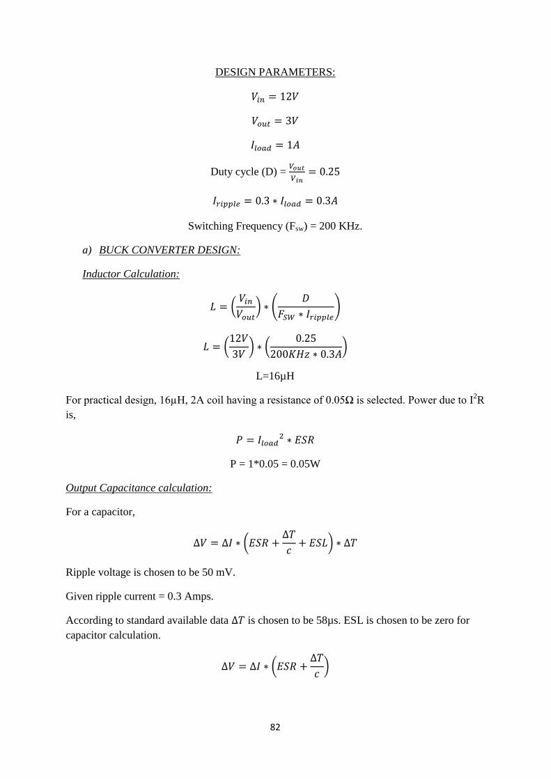
82
DESIGN PARAMETERS:
Duty cycle (D) =
Switching Frequency (Fsw) = 200 KHz.
a) BUCK CONVERTER DESIGN:
Inductor Calculation:
(
) (
)
(
) (
)
L=16µH
For practical design, 16µH, 2A coil having a resistance of 0.05Ω is selected. Power due to I2R
is,
P = 1*0.05 = 0.05W
Output Capacitance calculation:
For a capacitor,
(
)
Ripple voltage is chosen to be 50 mV.
Given ripple current = 0.3 Amps.
According to standard available data is chosen to be 58µs. ESL is chosen to be zero for
capacitor calculation.
(
)
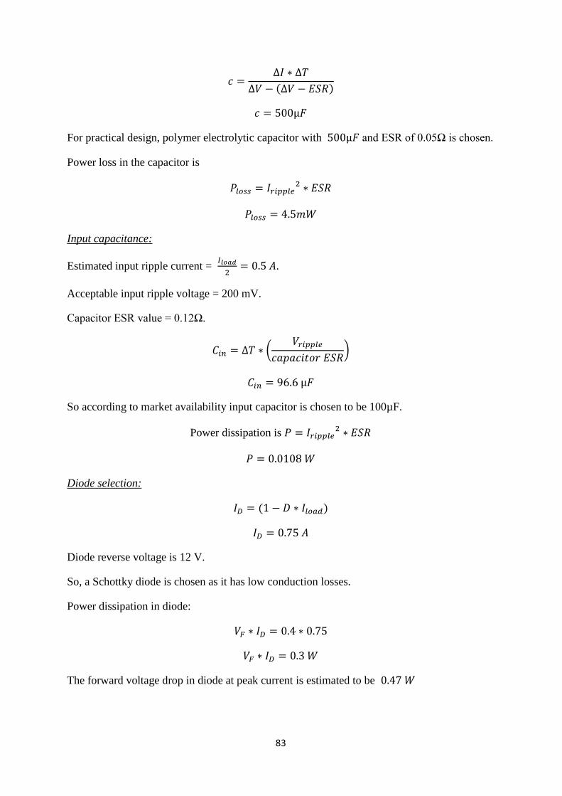
83
For practical design, polymer electrolytic capacitor with and ESR of 0.05Ω is chosen.
Power loss in the capacitor is
Input capacitance:
Estimated input ripple current =
.
Acceptable input ripple voltage = 200 mV.
Capacitor ESR value = 0.12Ω.
(
)
So according to market availability input capacitor is chosen to be 100µF.
Power dissipation is
Diode selection:
Diode reverse voltage is 12 V.
So, a Schottky diode is chosen as it has low conduction losses.
Power dissipation in diode:
The forward voltage drop in diode at peak current is estimated to be
84
MOSFET Selection:
An N-channel MOSFET with input voltage 12 V, 1 Amp load current,
and switching frequency = 200KHz. of the MOSFET is 0.02Ω.
Conduction loss =
Conduction loss = 5mW.
(
)
Buck converter efficiency:
Power output = 3W (3V@1A)
Input capacitor loss = 0.0108 W
Output capacitor loss = 4.5 mW
Diode loss = 300mW
Inductor loss = 0.05 W
MOSFET loss = 75mW
Total loss = 440mW.
Here diode losses are almost 60 percent of total losses, because of forward voltage drop of 0.4
volts. Here diode commutation is independent of MOSFET switching. So this is called
“ASYNCHRONOUS BUCK CONVERTER”.

85
PAPERS PUBLISHED:
1. B.Chitti Babu, S.R.Samantaray, Nikhil Saraogi, M.V. Ashwin Kumar, R.
Sriharsha and S.Karmakar ,”Synchronous Buck Converter based PV Energy
System for Portable Applications”, Proc., of 2011 IEEE Students’ Technology
Symposium, TECHSYM 2011. ISBN: 978-1-4244-8942-8.
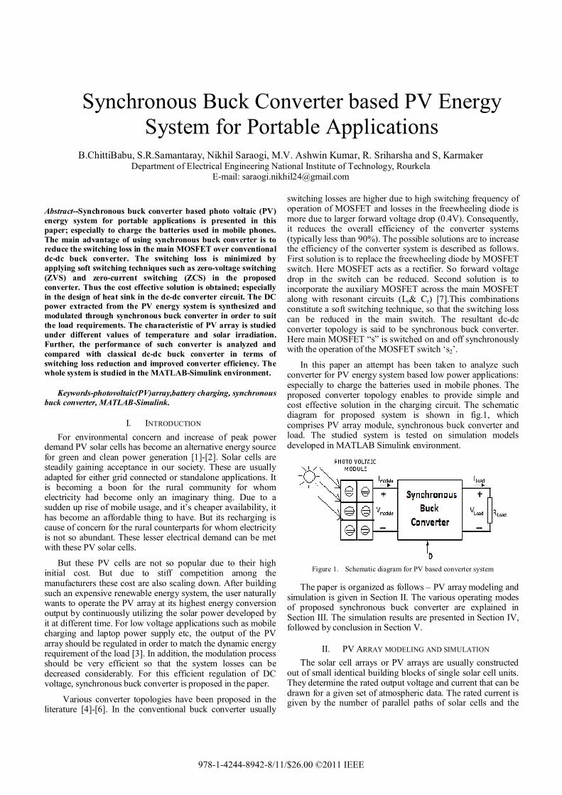
Abstract--Synchronous buck converter based photo voltaic (PV) energy system for portable applications is presented in this paper; especially to charge the batteries used in mobile phones. The main advantage of using synchronous buck converter is to reduce the switching loss in the main MOSFET over conventional dc-dc buck converter. The switching loss is minimized by applying soft switching techniques such as zero-voltage switching (ZVS) and zero-current switching (ZCS) in the proposed converter. Thus the cost effective solution is obtained; especially in the design of heat sink in the dc-dc converter circuit. The DC power extracted from the PV energy system is synthesized and modulated through synchronous buck converter in order to suit the load requirements. The characteristic of PV array is studied under different values of temperature and solar irradiation. Further, the performance of such converter is analyzed and compared with classical dc-dc buck converter in terms of switching loss reduction and improved converter efficiency. The whole system is studied in the MATLAB-Simulink environment.
Keywords-photovoltaic(PV)array,battery charging, synchronous buck converter, MATLAB-Simulink.
I. INTRODUCTION
For environmental concern and increase of peak power demand PV solar cells has become an alternative energy source for green and clean power generation [1]-[2]. Solar cells are steadily gaining acceptance in our society. These are usually adapted for either grid connected or standalone applications. It is becoming a boon for the rural community for whom electricity had become only an imaginary thing. Due to a sudden up rise of mobile usage, and it’s cheaper availability, it has become an affordable thing to have. But its recharging is cause of concern for the rural counterparts for whom electricity is not so abundant. These lesser electrical demand can be met with these PV solar cells.
But these PV cells are not so popular due to their high initial cost. But due to stiff competition among the manufacturers these cost are also scaling down. After building such an expensive renewable energy system, the user naturally wants to operate the PV array at its highest energy conversion output by continuously utilizing the solar power developed by it at different time. For low voltage applications such as mobile charging and laptop power supply etc, the output of the PV array should be regulated in order to match the dynamic energy requirement of the load [3]. In addition, the modulation process should be very efficient so that the system losses can be decreased considerably. For this efficient regulation of DC voltage, synchronous buck converter is proposed in the paper.
Various converter topologies have been proposed in the literature [4]-[6]. In the conventional buck converter usually
switching losses are higher due to high switching frequency of operation of MOSFET and losses in the freewheeling diode is more due to larger forward voltage drop (0.4V). Consequently, it reduces the overall efficiency of the converter systems (typically less than 90%). The possible solutions are to increase the efficiency of the converter system is described as follows. First solution is to replace the freewheeling diode by MOSFET switch. Here MOSFET acts as a rectifier. So forward voltage drop in the switch can be reduced. Second solution is to incorporate the auxiliary MOSFET across the main MOSFET along with resonant circuits (Lr& Cr) [7].This combinations constitute a soft switching technique, so that the switching loss can be reduced in the main switch. The resultant dc-dc converter topology is said to be synchronous buck converter. Here main MOSFET “s” is switched on and off synchronously with the operation of the MOSFET switch ‘s2’.
In this paper an attempt has been taken to analyze such converter for PV energy system based low power applications: especially to charge the batteries used in mobile phones. The proposed converter topology enables to provide simple and cost effective solution in the charging circuit. The schematic diagram for proposed system is shown in fig.1, which comprises PV array module, synchronous buck converter and load. The studied system is tested on simulation models developed in MATLAB Simulink environment.
Figure 1. Schematic diagram for PV based converter system
The paper is organized as follows – PV array modeling and simulation is given in Section II. The various operating modes of proposed synchronous buck converter are explained in Section III. The simulation results are presented in Section IV, followed by conclusion in Section V.
II. PV ARRAY MODELING AND SIMULATION
The solar cell arrays or PV arrays are usually constructed out of small identical building blocks of single solar cell units. They determine the rated output voltage and current that can be drawn for a given set of atmospheric data. The rated current is given by the number of parallel paths of solar cells and the
Synchronous Buck Converter based PV Energy System for Portable Applications
B.ChittiBabu, S.R.Samantaray, Nikhil Saraogi, M.V. Ashwin Kumar, R. Sriharsha and S, Karmaker Department of Electrical Engineering National Institute of Technology, Rourkela
E-mail: [email protected]
978-1-4244-8942-8/11/$26.00 ©2011 IEEE
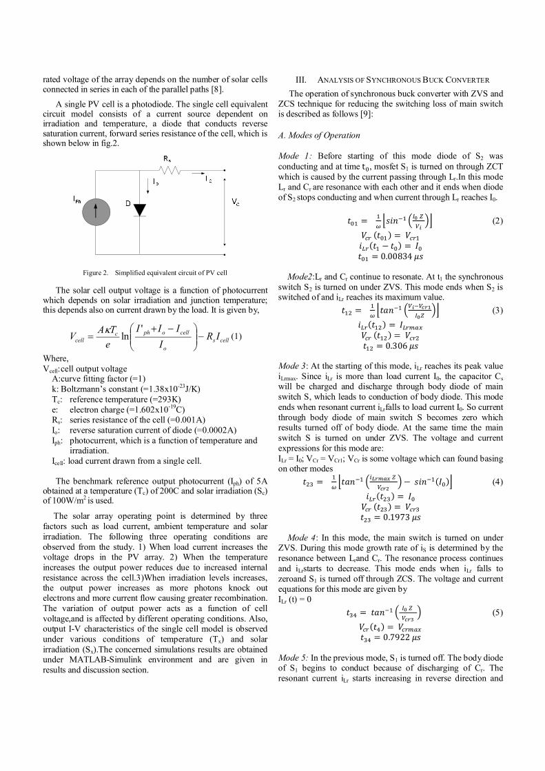
rated voltage of the array depends on the number of solar cells connected in series in each of the parallel paths [8].
A single PV cell is a photodiode. The single cell equivalent circuit model consists of a current source dependent on irradiation and temperature, a diode that conducts reverse saturation current, forward series resistance of the cell, which is shown below in fig.2.
Figure 2. Simplified equivalent circuit of PV cell
The solar cell output voltage is a function of photocurrent which depends on solar irradiation and junction temperature; this depends also on current drawn by the load. It is given by,
cells
o
cellophccell IR
I
III
e
TAV
'ln
(1)
Where, Vcell: cell output voltage
A:curve fitting factor (=1) k: Boltzmann’s constant (=1.38x10⁻²³J/K) Tc: reference temperature (=293K) e: electron charge (=1.602x10⁻¹⁹C) Rs: series resistance of the cell (=0.001A) Io: reverse saturation current of diode (=0.0002A) Iph: photocurrent, which is a function of temperature and
irradiation. Icell: load current drawn from a single cell.
The benchmark reference output photocurrent (Iph) of 5A
obtained at a temperature (Tc) of 200C and solar irradiation (Sc) of 100W/m2 is used.
The solar array operating point is determined by three factors such as load current, ambient temperature and solar irradiation. The following three operating conditions are observed from the study. 1) When load current increases the voltage drops in the PV array. 2) When the temperature increases the output power reduces due to increased internal resistance across the cell.3)When irradiation levels increases, the output power increases as more photons knock out electrons and more current flow causing greater recombination. The variation of output power acts as a function of cell voltage,and is affected by different operating conditions. Also, output I-V characteristics of the single cell model is observed under various conditions of temperature (Tx) and solar irradiation (Sx).The concerned simulations results are obtained under MATLAB-Simulink environment and are given in results and discussion section.
III. ANALYSIS OF SYNCHRONOUS BUCK CONVERTER
The operation of synchronous buck converter with ZVS and ZCS technique for reducing the switching loss of main switch is described as follows [9]:
A. Modes of Operation Mode 1: Before starting of this mode diode of S2 was conducting and at time t, mosfet S1 is turned on through ZCT which is caused by the current passing through Lr.In this mode Lr and Cr are resonance with each other and it ends when diode of S2 stops conducting and when current through Lr reaches I0.
=
(2)
() = ( − ) = = 0.00834
Mode2:Lr and Cr continue to resonate. At t1 the synchronous switch S2 is turned on under ZVS. This mode ends when S2 is switched of and iLr reaches its maximum value.
=
(3)
() = () = = 0.306
Mode 3: At the starting of this mode, iLr reaches its peak value iLrmax. Since iLr is more than load current I0, the capacitor Cs
will be charged and discharge through body diode of main switch S, which leads to conduction of body diode. This mode ends when resonant current iLrfalls to load current I0. So current through body diode of main switch S becomes zero which results turned off of body diode. At the same time the main switch S is turned on under ZVS. The voltage and current expressions for this mode are: ILr = I0; VCr = VCr1; VCr is some voltage which can found basing on other modes
=
− () (4)
() = () = = 0.1973
Mode 4: In this mode, the main switch is turned on under
ZVS. During this mode growth rate of iS is determined by the resonance between Lrand Cr. The resonance process continues and iLrstarts to decrease. This mode ends when iLr falls to zeroand S1 is turned off through ZCS. The voltage and current equations for this mode are given by ILr (t) = 0
=
(5)
() = = 0.7922
Mode 5: In the previous mode, S1 is turned off. The body diode of S1 begins to conduct because of discharging of Cr. The resonant current iLr starts increasing in reverse direction and
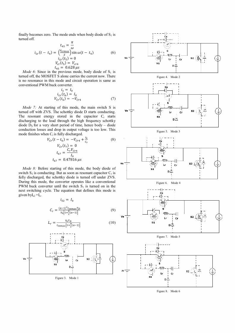
finally becomes zero. The mode ends when body diode of S1 is turned off.
=
( − ) =
sin ( − ) (6)
() = 0 () =
= 0.628 Mode 6: Since in the previous mode, body diode of S1 is
turned off, the MOSFET S alone carries the current now. There is no resonance in this mode and circuit operation is same as conventional PWM buck converter.
= () =
() = − (7)
Mode 7: At starting of this mode, the main switch S is turned off with ZVS. The schottky diode D starts conducting. The resonant energy stored in the capacitor Cr starts discharging to the load through the high frequency schottky diode DS for a very short period of time, hence body – diode conduction losses and drop in output voltage is too low. This mode finishes when Cr is fully discharged.
( − ) = − +
(8)
() = 0
=
= 0.47816
Mode 8: Before starting of this mode, the body diode of switch S2 is conducting. But as soon as resonant capacitor Cr is fully discharged, the schottky diode is turned off under ZVS. During this mode, the converter operates like a conventional PWM buck converter until the switch S1 is turned on in the next switching cycle. The equation that defines this mode is given byIs2 =Io.
=
=()
()
(9)
=
()
(10)
Figure 3. Mode 1
Figure 4. Mode 2
Figure 5. Mode 3
Figure 6. Mode 4
Figure 7. Mode 5
Figure 8. Mode 6
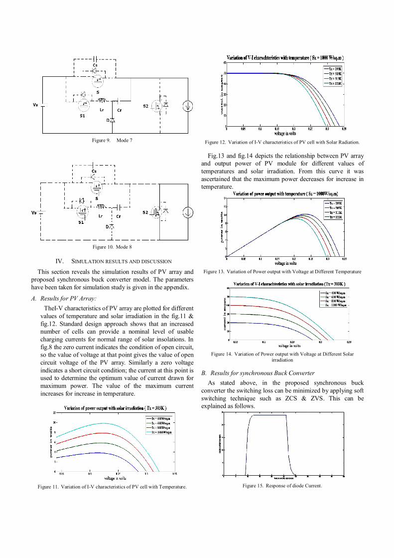
Figure 9. Mode 7
Figure 10. Mode 8
IV. SIMULATION RESULTS AND DISCUSSION
This section reveals the simulation results of PV array and proposed synchronous buck converter model. The parameters have been taken for simulation study is given in the appendix.
A. Results for PV Array:
TheI-V characteristics of PV array are plotted for different values of temperature and solar irradiation in the fig.11 & fig.12. Standard design approach shows that an increased number of cells can provide a nominal level of usable charging currents for normal range of solar insolations. In fig.8 the zero current indicates the condition of open circuit, so the value of voltage at that point gives the value of open circuit voltage of the PV array. Similarly a zero voltage indicates a short circuit condition; the current at this point is used to determine the optimum value of current drawn for maximum power. The value of the maximum current increases for increase in temperature.
Figure 11. Variation of I-V characteristics of PV cell with Temperature.
Figure 12. Variation of I-V characteristics of PV cell with Solar Radiation.
Fig.13 and fig.14 depicts the relationship between PV array and output power of PV module for different values of temperatures and solar irradiation. From this curve it was ascertained that the maximum power decreases for increase in temperature.
Figure 13. Variation of Power output with Voltage at Different Temperature
Figure 14. Variation of Power output with Voltage at Different Solar
irradiation
B. Results for synchronous Buck Converter
As stated above, in the proposed synchronous buck converter the switching loss can be minimized by applying soft switching technique such as ZCS & ZVS. This can be explained as follows.
Figure 15. Response of diode Current.
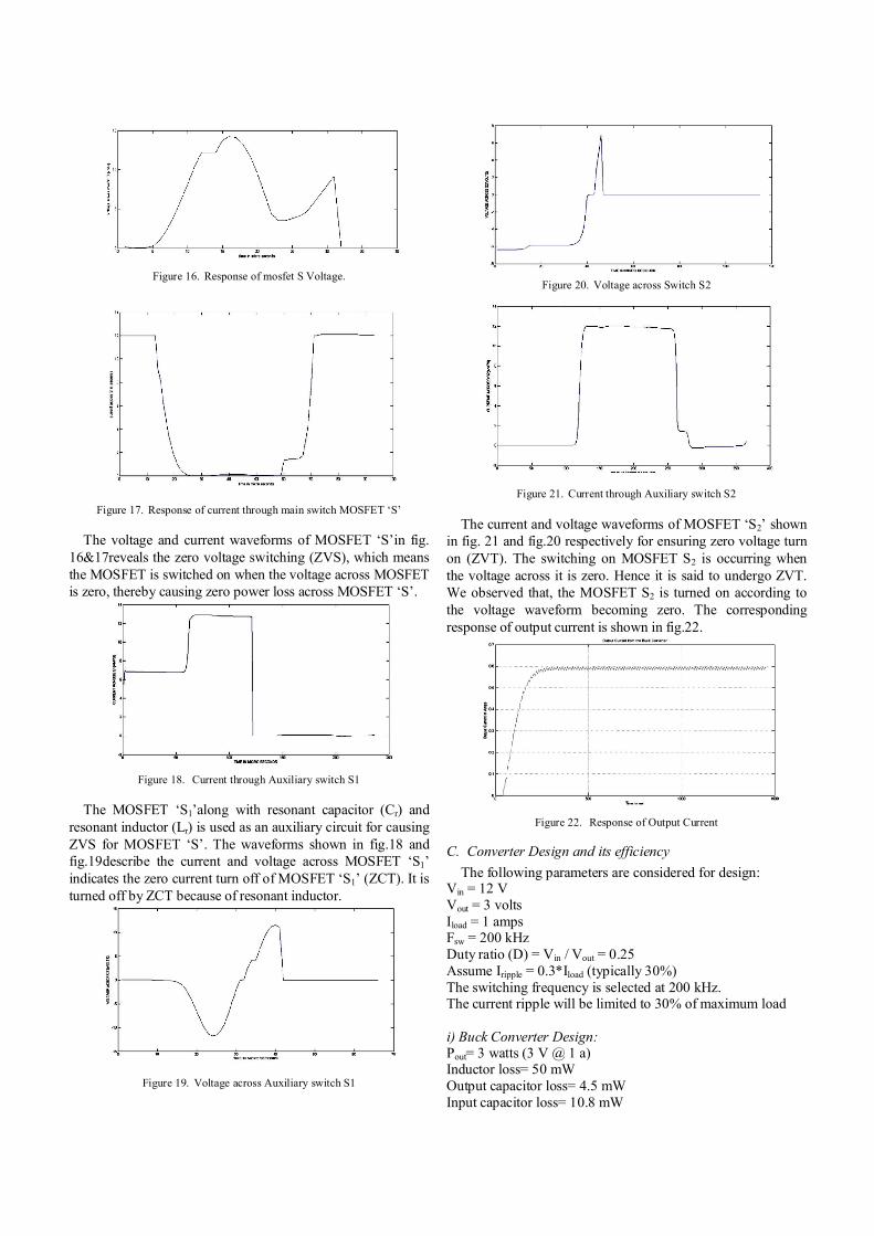
Figure 16. Response of mosfet S Voltage.
Figure 17. Response of current through main switch MOSFET ‘S’
The voltage and current waveforms of MOSFET ‘S’in fig. 16&17reveals the zero voltage switching (ZVS), which means the MOSFET is switched on when the voltage across MOSFET is zero, thereby causing zero power loss across MOSFET ‘S’.
Figure 18. Current through Auxiliary switch S1
The MOSFET ‘S1’along with resonant capacitor (Cr) and resonant inductor (Lr) is used as an auxiliary circuit for causing ZVS for MOSFET ‘S’. The waveforms shown in fig.18 and fig.19describe the current and voltage across MOSFET ‘S1’ indicates the zero current turn off of MOSFET ‘S1’ (ZCT). It is turned off by ZCT because of resonant inductor.
Figure 19. Voltage across Auxiliary switch S1
Figure 20. Voltage across Switch S2
Figure 21. Current through Auxiliary switch S2
The current and voltage waveforms of MOSFET ‘S2’ shown in fig. 21 and fig.20 respectively for ensuring zero voltage turn on (ZVT). The switching on MOSFET S2 is occurring when the voltage across it is zero. Hence it is said to undergo ZVT. We observed that, the MOSFET S2 is turned on according to the voltage waveform becoming zero. The corresponding response of output current is shown in fig.22.
Figure 22. Response of Output Current
C. Converter Design and its efficiency
The following parameters are considered for design: Vin = 12 V Vout = 3 volts Iload = 1 amps Fsw = 200 kHz Duty ratio (D) = Vin / Vout = 0.25 Assume Iripple = 0.3*Iload (typically 30%) The switching frequency is selected at 200 kHz. The current ripple will be limited to 30% of maximum load i) Buck Converter Design: Pout= 3 watts (3 V @ 1 a) Inductor loss= 50 mW Output capacitor loss= 4.5 mW Input capacitor loss= 10.8 mW
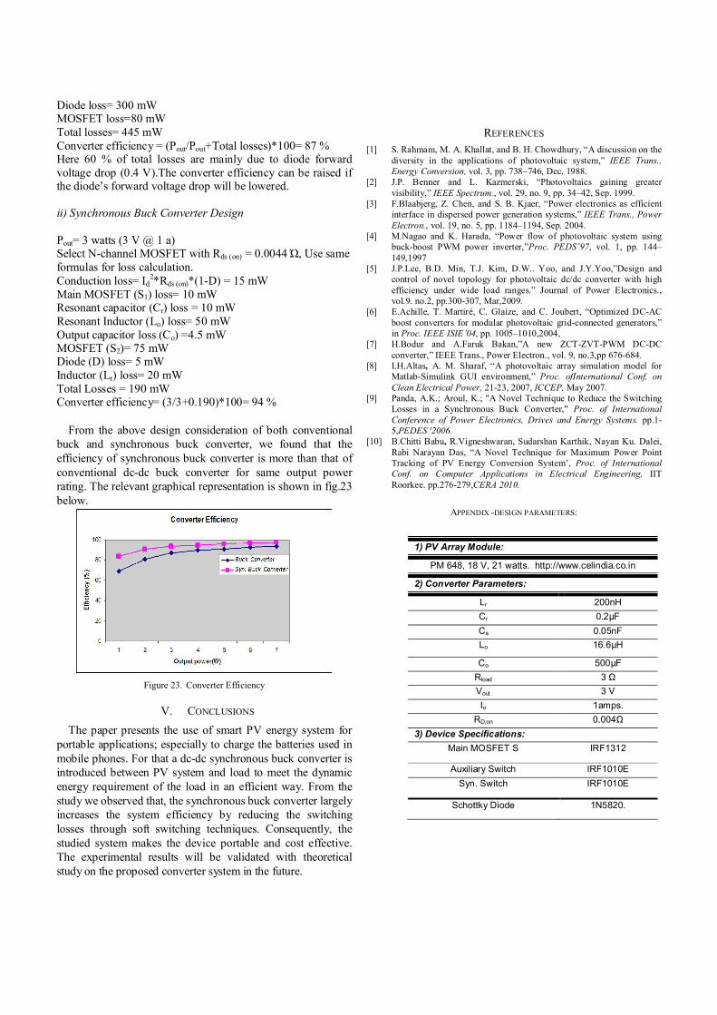
Diode loss= 300 mW MOSFET loss=80 mW Total losses= 445 mW Converter efficiency = (Pout/Pout+Total losses)*100= 87 % Here 60 % of total losses are mainly due to diode forward voltage drop (0.4 V).The converter efficiency can be raised if the diode’s forward voltage drop will be lowered. ii) Synchronous Buck Converter Design Pout= 3 watts (3 V @ 1 a) Select N-channel MOSFET with Rds (on) = 0.0044 Ώ, Use same formulas for loss calculation. Conduction loss= Id
2*Rds (on)*(1-D) = 15 mW Main MOSFET (S1) loss= 10 mW Resonant capacitor (Cr) loss = 10 mW Resonant Inductor (Lo) loss= 50 mW Output capacitor loss (Co) =4.5 mW MOSFET (S2)= 75 mW Diode (D) loss= 5 mW Inductor (Lr) loss= 20 mW Total Losses = 190 mW Converter efficiency= (3/3+0.190)*100= 94 %
From the above design consideration of both conventional buck and synchronous buck converter, we found that the efficiency of synchronous buck converter is more than that of conventional dc-dc buck converter for same output power rating. The relevant graphical representation is shown in fig.23 below.
Figure 23. Converter Efficiency
V. CONCLUSIONS
The paper presents the use of smart PV energy system for portable applications; especially to charge the batteries used in mobile phones. For that a dc-dc synchronous buck converter is introduced between PV system and load to meet the dynamic energy requirement of the load in an efficient way. From the study we observed that, the synchronous buck converter largely increases the system efficiency by reducing the switching losses through soft switching techniques. Consequently, the studied system makes the device portable and cost effective. The experimental results will be validated with theoretical study on the proposed converter system in the future.
REFERENCES
[1] S. Rahmam, M. A. Khallat, and B. H. Chowdhury, “A discussion on the diversity in the applications of photovoltaic system,” IEEE Trans., Energy Conversion, vol. 3, pp. 738–746, Dec. 1988.
[2] J.P. Benner and L. Kazmerski, “Photovoltaics gaining greater visibility,” IEEE Spectrum., vol. 29, no. 9, pp. 34–42, Sep. 1999.
[3] F.Blaabjerg, Z. Chen, and S. B. Kjaer, “Power electronics as efficient interface in dispersed power generation systems,” IEEE Trans., Power Electron., vol. 19, no. 5, pp. 1184–1194, Sep. 2004.
[4] M.Nagao and K. Harada, “Power flow of photovoltaic system using buck-boost PWM power inverter,”Proc. PEDS’97, vol. 1, pp. 144–149,1997
[5] J.P.Lee, B.D. Min, T.J. Kim, D.W.. Yoo, and J.Y.Yoo,”Design and control of novel topology for photovoltaic dc/dc converter with high efficiency under wide load ranges.” Journal of Power Electronics., vol.9. no.2, pp.300-307, Mar,2009.
[6] E.Achille, T. Martiré, C. Glaize, and C. Joubert, “Optimized DC-AC boost converters for modular photovoltaic grid-connected generators,” in Proc. IEEE ISIE’04, pp. 1005–1010,2004,
[7] H.Bodur and A.Faruk Bakan,”A new ZCT-ZVT-PWM DC-DC converter,” IEEE Trans., Power Electron., vol. 9, no.3,pp 676-684.
[8] I.H.Altas, A. M. Sharaf, “A photovoltaic array simulation model for Matlab-Simulink GUI environment,” Proc. ofInternational Conf. on Clean Electrical Power, 21-23, 2007, ICCEP, May 2007.
[9] Panda, A.K.; Aroul, K.; "A Novel Technique to Reduce the Switching Losses in a Synchronous Buck Converter," Proc. of International Conference of Power Electronics, Drives and Energy Systems. pp.1-5,PEDES '2006.
[10] B.Chitti Babu, R.Vigneshwaran, Sudarshan Karthik, Nayan Ku. Dalei, Rabi Narayan Das, “A Novel Technique for Maximum Power Point Tracking of PV Energy Conversion System’, Proc. of International Conf. on Computer Applications in Electrical Engineering, IIT Roorkee. pp.276-279,CERA 2010.
APPENDIX -DESIGN PARAMETERS:
1) PV Array Module:
PM 648, 18 V, 21 watts. http://www.celindia.co.in
2) Converter Parameters:
Lr 200nH
Cr 0.2µF
Cs 0.05nF
Lo 16.6µH
Co 500µF
Rload 3 Ω
Vout 3 V
Io 1amps.
RD,on 0.004Ω
3) Device Specifications:
Main MOSFET S IRF1312
Auxiliary Switch IRF1010E
Syn. Switch IRF1010E
Schottky Diode 1N5820.
Related Documents