DESIGN AND IMPLEMENTATION OF AUTOMATIC PHASE CHANGER By Md Atiqul Islam B.Sc., Khulna University of Engineering & Technology, Khulna, Bangladesh, 2008 A project report presented to Ryerson University in partial fulfillment of the requirements for the degree of Master of Engineering in the program of Electrical and Computer Engineering Toronto, Ontario, Canada, 2017 © Md Atiqul Islam, 2017

Welcome message from author
This document is posted to help you gain knowledge. Please leave a comment to let me know what you think about it! Share it to your friends and learn new things together.
Transcript

DESIGN AND IMPLEMENTATION OF AUTOMATIC PHASE CHANGER
By
Md Atiqul Islam
B.Sc., Khulna University of Engineering & Technology, Khulna, Bangladesh, 2008
A project report
presented to Ryerson University
in partial fulfillment of the
requirements for the degree of
Master of Engineering
in the program of
Electrical and Computer Engineering
Toronto, Ontario, Canada, 2017
© Md Atiqul Islam, 2017

ii
AUTHOR'S DECLARATION
I hereby declare that I am the sole author of this project. This is a true copy of the project, including any
required final revisions.
I authorize Ryerson University to lend this project to other institutions or individuals for the purpose of
scholarly research.
I further authorize Ryerson University to reproduce this project by photocopying or by other means, in total
or in part, at the request of other institutions or individuals for the purpose of scholarly research.
I understand that my project may be made electronically available to the public.

iii
DESIGN AND IMPLEMENTATION OF AUTOMATIC PHASE CHANGER
Md Atiqul Islam
Master of Engineering
Electrical and Computer Engineering Ryerson University, Toronto, 2017
ABSTRACT
Simulation of an Automatic Phase Changer (APC) circuit was performed in this project. The simulation
was carried out using Proteus 8. Automatic Phase Changer (APC) automatically changes the phase as the
name suggests. In three phase power system 3 inputs of APC circuit are connected to three phases of the
system and its three outputs are connected to three different loads. These three loads always need their
normal rated voltage for proper operation. Results observed that if voltage of any phase goes below the
nominal rating the loads may malfunction. Here, Automatic Phase Changer comes into action. When a
phase voltage goes below its nominal rating, APC provides correct level of voltage to the load connected to
that phase.
KEYWORDS: Relay, Switch, Comparator, Phase Changer, Automatic

iv
ACKNOWLEDGEMENTS
I would like to express my deepest appreciation to all those who provided me the possibility to complete
this report. A special gratitude goes to my project Supervisor, Professor. Vadim Geurkov, whose
suggestions and encouragement, helped me to a lot to conduct my project especially in writing this report.
Furthermore, I would also like to acknowledge with much appreciation the crucial role of all staff of Ryerson
University – Toronto, Canada, who gave the permission to use all required equipment and the necessary
materials to complete the task in laboratory room. Special thanks goes to Md Golam Kibria; Post-Doctoral
Fellow, Department of Electrical and Computer Engineering, University of Toronto to who helped me to
assemble the parts and gave suggestion about the task. Last but not least, many thanks go to the external
supervisor of the project, Professor Dr. Andy Ye, Associate Professor, Department of Electrical and
Computer Engineering who have invested his effort to evaluate this project report and gave important
suggestions regarding project circuit. I would like to appreciate the guidance given by other teachers as well
as the panels especially during project presentation that helped me to improve the presentation skills through
their valuable comments and advices.

v
To my Loved Ones

vi
TABLE OF CONTENTS
AUTHOR'S DECLARATION ...................................................................................................................... ii
ABSTRACT ................................................................................................................................................. iii
ACKNOWLEDGEMENTS ......................................................................................................................... iv
LIST OF TABLES ....................................................................................................................................... vi
LIST OF FIGURES ..................................................................................................................................... vi
CHAPTER 1
1.1 Introduction ............................................................................................................................................. 1
1.2 Advantage over Traditional Method ....................................................................................................... 1
1.3 Objective of this Work ............................................................................................................................ 1
1.3.1 Primary objectives ............................................................................................................................... 2
1.3.2 Secondary Objectives ........................................................................................................................... 2
1.4 Overview of this Project ......................................................................................................................... 2
CHAPTER 2
Modeling of Automatic Phase Changer ........................................................................................................ 3
2.1 Necessity of Automatic Phase Changer .................................................................................................. 3
2.2 Circuit Description and Analysis ............................................................................................................ 3
2.3 Block Diagram ........................................................................................................................................ 5
2.4 Summary ................................................................................................................................................. 6
CHAPTER 3
Main Components Feature ............................................................................................................................ 7
3.1 Introduction ............................................................................................................................................. 7
3.2 Diode ....................................................................................................................................................... 7
3.3 Zener Diode ............................................................................................................................................ 9
3.3.1 Zener Region ...................................................................................................................................... 10
3.4 BJT ........................................................................................................................................................ 11
3.4.1 PNP Transistor ................................................................................................................................... 11
3.4.2 NPN Transistor .................................................................................................................................. 12
3.5 Operational Amplifier ........................................................................................................................... 13
3.5.1 Characteristic of an ideal Op-amp (741IC) ........................................................................................ 14
3.5.2 Properties of an ideal Op-amp (741IC) .............................................................................................. 15
3.5.3 Practical Op-amp Circuit ................................................................................................................... 15
3.5.3.1 Voltage Follower (Buffer) .............................................................................................................. 15
3.5.3.2 Inverting Amplifier ......................................................................................................................... 16

vii
3.5.3.3 Non-inverting Amplifier ................................................................................................................. 16
3.5.3.4 Summing Amplifier ........................................................................................................................ 17
3.5.3.5 Comparator ..................................................................................................................................... 17
3.6 Using 741 Op-amp as a comparator ...................................................................................................... 18
3.7 Transformer........................................................................................................................................... 19
3.7.1 Transformer cores .............................................................................................................................. 20
3.7.2 Classification of transformer .............................................................................................................. 21
3.7.3 Step-up transformer ........................................................................................................................... 22
3.7.4 Step-down Transformer ..................................................................................................................... 23
3.8 Relay ..................................................................................................................................................... 24
3.8.1 Pin Configuration of Relay ................................................................................................................ 25
3.8.2 Working principle of Relay................................................................................................................ 26
3.9 Specific work of Transformer, Diode, Capacitor, Zener Diode, Op-amp, BJT and Relay in the main
circuit .......................................................................................................................................................... 27
3.10. Summary ............................................................................................................................................ 28
CHAPTER 4
Simulation and Result ................................................................................................................................. 29
4.1 Introduction ........................................................................................................................................... 29
4.2 Electronic Simulation Software: Proteus 8 Professional ...................................................................... 29
4.3 Simulation of the APC circuit ............................................................................................................... 30
4.3.1 All three phases have nominal voltage ratings (120V, 60 Hz) .......................................................... 30
4.3.2 Any one phase has voltage below the nominal rating (<120V) ......................................................... 31
4.3.3 Any two phases have voltage below the nominal rating (<120V) ..................................................... 33
4.4 Results of Simulation ............................................................................................................................ 37
4.5 Summary ............................................................................................................................................... 38
CHAPTER 5
Conclusion and Future Directions............................................................................................................... 39
5.1 Limitation of this study ......................................................................................................................... 39
5.2 Conclusions ........................................................................................................................................... 39
5.3 Directions for the future work ............................................................................................................... 40
Appendix A ....................................................................................................................................41
Datasheet of the Chips used in the circuit ................................................................................................... 41
REFERENCES ........................................................................................................................................... 46

vi
LIST OF TABLES
Table 4. 1: Results from the simulation for each possible situation. .......................................................... 37

vi
LIST OF FIGURES
Figure 2. 1: Automatic Phase Changer. [3] ................................................................................................... 4
Figure 2. 2: Block Diagram of Automatic Phase Changer. [4] ..................................................................... 5
Figure 3. 1: Diode [5] .................................................................................................................................... 7
Figure 3. 2: Diode in Forward Bias Condition [7] ........................................................................................ 8
Figure 3. 3: Diode in Reverse Bias Condition [7] ......................................................................................... 8
Figure 3. 4: Diode Characteristics [5] ........................................................................................................... 9
Figure 3. 5: Zener Diode [5] ....................................................................................................................... 10
Figure 3. 6: Zener Regions [5] .................................................................................................................... 10
Figure 3. 7: BJT [5] ..................................................................................................................................... 11
Figure 3. 8: PNP Transistor [10] ................................................................................................................. 12
Figure 3. 9: NPN Transistor [9] .................................................................................................................. 13
Figure 3. 10: 741 IC [5] .............................................................................................................................. 13
Figure 3. 11: Pin Configuration of 741 IC [6] ............................................................................................ 14
Figure 3. 12: Voltage Follower [14] ........................................................................................................... 15
Figure 3. 13: Inverting Amplifier [5] .......................................................................................................... 16
Figure 3. 14: Non-inverting Amplifier [5] .................................................................................................. 16
Figure 3. 15: Summing Amplifier [11] ....................................................................................................... 17
Figure 3. 16: comparator [15] ..................................................................................................................... 17
Figure 3. 17: Op-amp comparator circuit [15] ............................................................................................ 19
Figure 3. 18: Transformer [16] ................................................................................................................... 20
Figure 3. 19: Transformer core [16]............................................................................................................ 21
Figure 3. 20: Step-up Transformer [17] ...................................................................................................... 23
Figure 3. 21: Step-down transformer [18] .................................................................................................. 24
Figure 3. 22: Relay [19] .............................................................................................................................. 25

vii
Figure 3. 23: Pin configuration of Relay [20] ............................................................................................. 25
Figure 3. 24: Relay Design [20] .................................................................................................................. 26
Figure 3. 25: Diode Rectification ................................................................................................................ 27
Figure 3. 26: Capacitor acting as a filter. .................................................................................................... 27
Figure 4. 1: Wiring the Automatic Phase Changer Circuit in Proteus 8 Professional................................ 29
Figure 4. 2: Voltage and current rating for phase – 1 (Upper) and voltage across load – 1 (L1, A bulb) for
this phase. 31
Figure 4. 3: Current through phase-3 when phase voltage is 117V (Upper). Voltage across load-3 (L3, A
bulb) is 84.4V (Rms value of 120V) (Lower). .................................................................................... 32
Figure 4. 4: Current through phase-1 is 7.06A (2×3.52A) because this phase also supplies load-3 as well
as load-1. 33
Figure 4. 5: Current through phase-2 is 0A and phase-2 voltage (V2) is 117V. ........................................ 34
Figure 4. 6: Voltage across load-2 (L2) is 84.3 V (rms value of 120V). ................................................... 34
Figure 4. 7: Current of phase-3 is 0A and voltage of phase-3 (V3) is 117V. ............................................. 35
Figure 4. 8: Voltage across load-3 (L3) is 84.3 V (rms value of 120V). .................................................... 35
Figure 4. 9: Current through phase-1 is 10.5A and phase-1 voltage (V1) is 120V. ................................... 36
Figure 4. 10: Voltage across load-1 (L1) is 84.4V (Rms value of 120V). ................................................. 36

1
CHAPTER 1
Introduction
1.1 Introduction
Power instability and phase failure has become a serious problem in the developing countries like
Bangladesh and Nigeria to improve their socio economic condition [2]. Almost all of the
companies; Industrial, commercial and also domestic loads are run by the public power supply
which associates different problems for example: imbalances among the phases, phase failure or
sometimes complete power shut down occurs due to various types of technical problems occurred
in the power generation, transmission and distribution system [3]. Most of the power consumers
use single phase equipment for operational purpose which is greatly affected if there is unbalance
voltages, under voltages or over voltages. A significant amount of time would be required for
manual switch over operation and as a result, serious trouble could be associated with the machines
or in the production process. Moreover, a standby manpower would always be required to change
over the supply voltage line. To overcome these challenges, Automatic phase changing system
could be implemented. Here, an Automatic Phase Changer circuit has been simulated.
1.2 Advantage over Traditional Method
Automatic phase changer finds wide application in modern world. During earlier days, if there was
any power failure in any one of three phases occurs, it was required to switch to the available phase
manually. By implementing automatic phase changer it automatically shifts to the phase where
correct voltage is available. It can be used in residences, small offices, buildings etc. Automatic
phase changer is a circuit of very compact design. This circuit is very cost effective. It is very easy
to install too. Low maintenance is required for this circuit.
1.3 Objective of this Work
In three-phase applications, if low voltage is occurred in any one or two phases then to maintain
normal voltage for the equipment this circuit can play an effective role. However, a proper-rating
fuse needs to be used in the input lines (R, Y and B) of each phase. The circuit provides correct
voltage in the same power supply lines through relays from the other phase where correct voltage
is available.

2
1.3.1 Primary objectives
The primary objective is to make the automatic phase changer circuit which will work for under
voltage fault in a three phage system and to show that by using this circuit, intensity & amplitude
of voltage in the load side will remain the same before the fault occur.
1.3.2 Secondary Objectives
The secondary objective is to show the simulation & to prove theoretically that the automatically
phase change circuit actually works for over voltage fault.
1.4 Overview of this Project
Chapter 2 discusses about the circuit diagram and explains the working principle of the Automatic
Phase Changer (APC). Chapter 3 discusses about the main components used in the APC circuit.
Simulation and its results are discussed in chapter 4. Chapter 5 discusses about main part of our
project – implementation and results. Results are shown in tables. In the final chapter conclusion,
the limitations of this circuit and future scopes are mentioned.

3
CHAPTER 2
Modeling of Automatic Phase Changer
2.1 Necessity of Automatic Phase Changer
In three phase power supply line voltage can be dropped or risen from the rated voltage supplied
in any phase for various causes. The reasons for voltage fluctuation are discussed below in brief.
Voltage rise: In case of transmission line is charged on no load- due to its capacitive effect
(Ferranti effect) voltage gets rise at receiving end more than that rated voltage.
Voltage drop: Due to active power loss or resistance of the line, IR drop occurs which result in
getting less voltage at the receiving end which is less than the rated voltage. Another reason for
voltage drop is that if heavy load is applied all of a sudden, voltage drop occurs.
Automatic Phase Changer circuit can provide nominal voltage to the emergency loads with the
help of healthy line. In the next portion, the principle of circuit operation is going to be described.
2.2 Circuit Description and Analysis
It is possible to supply current of correct voltage level in all the phases with this through relays if
proper voltage is available in any phase. Using it all the equipment can be operated smoothly when
correct voltage is available on a single phase in the building. The circuit is made mainly using a
comparator, transformer, transistor and relay. Three identical sets of the circuit, one each for three
phases, are used.

4
Figure 2. 1: Automatic Phase Changer. [3]
From Figure 2.1, when 120V is given to the input side of each of the transformers X1, X2 and X3.
It turns in 12Vdc in the output side of the transformers. The diodes D1, D2, D3, D4, D5, and D6
are used here to rectify the sinusoidal signal to dc signal. In this circuit seven capacitors (C1, C2,
C3, C4, C5, C6, and C7) are used. Capacitor C1, C2, C3, and C4 makes the output signal of
transformer smooth to make exact 12V dc. Whereas other capacitors (which are connected to relay
in parallel) make some delay to connect the correct line to load safely through relay. When the
12V dc voltage goes across R1 resistor some voltage gets dropped. In this circuit IC1, IC2 and IC3
work as comparator; those are 741 Op-amps. The voltage taken from the voltage divider circuit of
resistor R1 and preset resistor VR1; where, VR1 is used to set the reference voltage according to
the requirement is applied at non-inverting pin 3 of operational amplifier IC1. The reference
voltage at inverting pin 2 is fixed to 5.1V through a zener diode ZD1. The voltage at non-inverting
pin 3 remains high at the normal condition. So the output of the comparator remains 12 V. As a
result the pnp transistor remains off. When any of the input phase voltage gets below 120 V the
voltage in pin 2 gets high then the non-inverting pin 3 and the output of the comparator goes low.
As a result the pnp transistor starts conducting current and relay RL1 energizes and load L1 is

5
disconnected from phase ‘R’ and connected to phase ‘Y’ through relay RL2. Similarly, the auto
phase-change of the remaining two phases ‘Y’ and phase ‘B’ can be explained.
2.3 Block Diagram
Figure 2. 2: Block Diagram of Automatic Phase Changer. [4]
There are 3 phases ‘R’, ‘Y’ and ‘B’ in three phase power supply line. From the block diagram of
Figure 2.2, step down transformer steps down the phase voltage at level which can be used for
biasing the electronic circuit. Then the voltage gets rectified and filtered by using diode and
capacitor to get smooth dc voltage. The voltage then bias the Op-Amp which works as a

6
comparator. Op-Amp senses the problem and activates or deactivates the relay. So, the phase
which voltage is below the 120 V gets connected to the other stabilized phase voltage by the relay.
And the whole system gets stabilized.
2.4 Summary
After simulating the whole circuit one or two phase voltages have been changed from the three
phase power supply and equal load voltages was obtained in the output. In the next chapter, it will
be described about the components used in the circuit.

7
CHAPTER 3
Main Components Feature
3.1 Introduction
In this chapter it will be discussed about Diode, Zener Diode, BJT, Op-amp, characteristic and
properties of Op-amp, Practical Op-amp circuit, Op-amp as comparator, Transformer, step- up and
step down transformer, Relay, working principle of relay and their specific work in the circuit.
3.2 Diode
A Diode is an electronic component with two-terminals and asymmetric conductance; it has low
resistance to current flow in one direction, and high resistance in the other. The semiconductor
diode is created by simply joining an n-type and p-type material together, just the joining of one
material with a majority carrier of electrons to one with a majority carrier of holes. Diodes are
physically very small in size and control small current up to about 100mA. Diodes generally have
a silver or black band at one end of their body to help identify which end is its cathode terminal.
Figure 3.1 shows a diode.
Figure 3. 1: Diode [5]
To obtain forward bias or “on” condition is it is needed to be applied positive potential to the p-
type material and the negative potential to the n-type material. Forward bias refers to the
application of voltage across the device such that the electric field at the junction is reduced. The

8
arrow in the symbol of diode points in the direction of conventional current flow through the diode.
That mean the diode will only conduct if a positive supply is connected to the Anode (A) terminal
and a negative supply is connected to the Cathode (K) terminal, thus only allowing current to flow
through the forward direction only. Forward bias will act like a short circuit switch. Figure 3.2
shows the diode in forward bias condition.
Figure 3. 2: Diode in Forward Bias Condition [7]
If an external potential of V volts is applied across p-n junction such that the position terminal is
connected to the n-type material and the negative terminal is connected to the p-type material. In
reverse bias the diode will block any current flowing through it and instead will act like an open
switch. Figure 3.3 shows diode reverse bias condition.
Figure 3. 3: Diode in Reverse Bias Condition [7]
Diodes will block any and all current flowing into the reverse direction, or just act like a short
circuit if current flow is forward. The most important diode characteristic is its current-voltage (I-
V) relationship. Figure 3.4 shows the I-V characteristic curve of diode. This defines what the
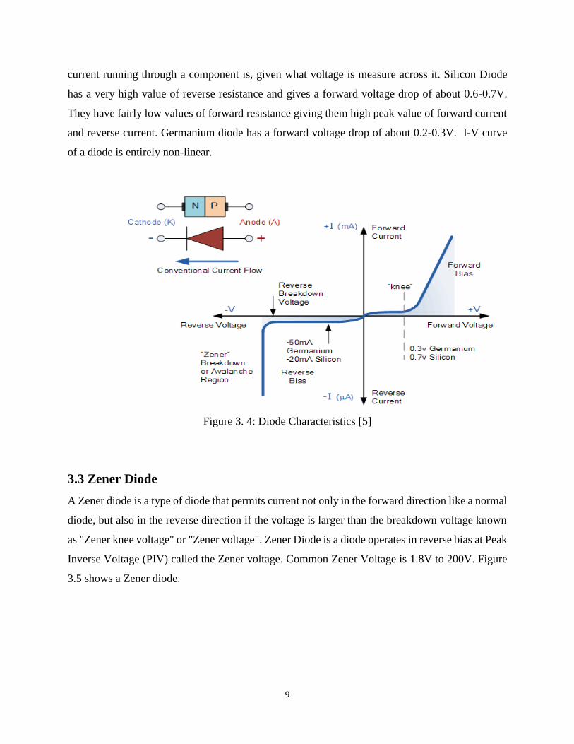
9
current running through a component is, given what voltage is measure across it. Silicon Diode
has a very high value of reverse resistance and gives a forward voltage drop of about 0.6-0.7V.
They have fairly low values of forward resistance giving them high peak value of forward current
and reverse current. Germanium diode has a forward voltage drop of about 0.2-0.3V. I-V curve
of a diode is entirely non-linear.
Figure 3. 4: Diode Characteristics [5]
3.3 Zener Diode
A Zener diode is a type of diode that permits current not only in the forward direction like a normal
diode, but also in the reverse direction if the voltage is larger than the breakdown voltage known
as "Zener knee voltage" or "Zener voltage". Zener Diode is a diode operates in reverse bias at Peak
Inverse Voltage (PIV) called the Zener voltage. Common Zener Voltage is 1.8V to 200V. Figure
3.5 shows a Zener diode.

10
Figure 3. 5: Zener Diode [5]
3.3.1 Zener Region
o The Diode is in the reverse biased condition.
o At some point the reverse biased voltage is so large the diode breaks down.
o The reverse current increases dramatically.
o This maximum voltage is called avalanche breakdown voltage & the current is called
avalanche current. Figure 3.6 shows the Zener Region.
Figure 3. 6: Zener Regions [5]

11
3.4 BJT
A Bipolar Junction Transistor (BJT) is a kind of transistor which operates through the contact of
two types of semiconductor. BJT s can be used as amplifier, switch or in oscillators. BJT has three
terminal connections to three doped semiconductor region. BJT is a three layer semi-conductor
device consisting of either two n-type or one p-type layer of material or two p-types and one n-
type layer of material. The former is called an NPN transistor and the latter is called PNP transistor.
In an NPN transistor, a thin and lightly doped p-type material is sandwiched between two thinker
n-type materials. While in a PNP transistor, a thin and lightly doped n-type material is sandwiched
between two thick p-type materials. Figure 3.7 shows NPN and PNP transistor.
(a) (b)
Figure 3. 7: BJT [5]
3.4.1 PNP Transistor
• The majority carriers in the emitter p-type material are holes.
• The base-emitter junction is forward biased to the majority carriers and the holes cross the
junction and appear in the base region.
• The base region is very thin and is only lightly doped with electrons so although some
electron-hole pairs are formed, many holes are left in the base region.

12
• The base-collector junction is reverse biased to electrons in the base region and holes in
the collector region, but forward biased to holes in the base region; these holes are attracted
by the negative potential at the collector terminal.
A large proportion of the holes in the base region cross the base-collector junction into the collector
region, creating a collector current; conventional current flow is in the direction of holes
movement. Figure 3.8 sows a PNP transistor.
Figure 3. 8: PNP Transistor [10]
3.4.2 NPN Transistor
• The majority carriers in the n-type emitter material are electron.
• The base-emitter junction is forward biased to these majority carriers and electron cross
the junction and appears in the base region.
• The property of base region is that it is very thin having lightly doped with holes, As a
result, a portion of recombination is occurred with holes but many electrons are found in
the base region.
• The base collector junction is reverse biased to hole in the base region and electrons in the
collector region, but is forward biased to electron in the base region, these electron are
attracted by the positive potential at the collector terminal.
• A large proportion of the electrons in the base region cross the base-collector junction into
the collector region, creating a collector current. Figure 3.9 shows a NPN transistor.

13
Figure 3. 9: NPN Transistor [9]
3.5 Operational Amplifier
An operational amplifier or op-amp is a high gain differential amplifier with high input
impendence and low output impedance. Op-amp is used to provide voltage amplitude changes
(amplitude & polarity), oscillator, filter circuit, comparator & many types of instrumentation
circuit. An op-amp contains a number of differential amplitude stages to achieve a very high
voltage gain. An operational amplifier is a DC coupled high gain electronic voltage amplifier with
a differential input and, usually a single ended output. An op-amp produces an output voltage that
is typically hundreds of thousands times larger than the voltage difference between its input
terminals. Figure 3.10 shows a 741 IC.
Figure 3. 10: 741 IC [5]

14
Among the available iintegrated circuit, operational amplifier is probably the most versatile. It is
very cheap especially keeping in mind the fact that it contains several hundred components. The
most common Op-amp is the 741 & it is used in much circuit. The op-amp is a linear amplifier
with an amazing variety of uses. Its main purpose is to amplify a weak signal. The 741 integrated
circuit looks like any other ‘chip’. However, it is a general purpose OP-AMP. It is required only
to know the basic information about its operation and use. The diagram opposite shows the pins
of the 741 OP-AMP. The important pins are 2, 3 and 6 because these represent inverting, non-
inverting and voltage out. Notice the triangular diagram that represents an Op-Amp integrated
circuit. Figure 3.11 shows the pin configuration of 741 IC.
Figure 3. 11: Pin Configuration of 741 IC [6]
3.5.1 Characteristic of an ideal Op-amp (741IC)
o Infinity gain.
o Infinity Bandwidth.
o Infinity Input impedance (between the two input terminals and from each terminal to
ground).
o Infinity output current drive capabilities.
o Zero output impedance.
o Zero input voltage offset.
o Zero input current.
o Common Mode Rejection Ratio (CMRR).
o The Slew Rate.

15
3.5.2 Properties of an ideal Op-amp (741IC)
o Infinite Open Loop gain
▪ The gain without feedback
▪ Equal to differential gain
o Infinite Input impedance
▪ Input current is almost 0A
▪ m-A input current in low-grade op-amp
o Zero Output Impedance
▪ act as perfect internal voltage source
▪ No internal resistance
▪ Output impedance in series with load
▪ Reducing output voltage to the load
▪ Practically, Rout ~ 20-100 W
3.5.3 Practical Op-amp Circuit
For having various operating characteristics, op-amp can be connected in a large number of
circuits. In this section, it will be covered few of the most common of these circuit connections.
3.5.3.1 Voltage Follower (Buffer)
The voltage follower circuit, as shown in figure 3.12, provides a gain of unity (1) with no polarity
or phase reversal. From the equivalent circuit (figure 3.12) it is clear that
Figure 3. 12: Voltage Follower [14]

16
3.5.3.2 Inverting Amplifier
The most widely used constant-gain amplifier is inverting amplifier, as shown in figure 3.13. The
output is obtained by multiplying the input by a fixed or constant gain, set by the input resistor R1
and feedback resistor Rf. This output also being inverted from the input. We can write,
Figure 3. 13: Inverting Amplifier [5]
3.5.3.3 Non-inverting Amplifier
The connection of figure 3.14 has shown an op-amp circuit that works as a non-inverting amplifier
or constant –gain multiplier. The voltage across R1 is Vin. This must be equal to the output voltage,
through a voltage divided of R1 and R2. The resulting relation will be
Figure 3. 14: Non-inverting Amplifier [5]

17
3.5.3.4 Summing Amplifier
Probably the most used of the op-amp is the summing amplifier circuit shown in figure 3.15. The
circuit shows a three input summing amplifier circuit. We can express the output voltage in terms
of the input as
Figure 3. 15: Summing Amplifier [11]
3.5.3.5 Comparator
A comparator is an electronic device which is used to compare two voltage or current and sends a
digital signal as output indicating which one is larger. The result of this comparator is indicated by
output voltage. Owing to its extremely large open-loop gain, op-amp has become an extremely
sensitive device for verifying its input with zero. In figure 3.16 if V1>V2 the output is driven to
the positive supply voltage and if V2<V1 it is driven to the negative supply voltage. The switching
time for - to + is limited by the slew rate of the op-amp. Figure 3.16 has shown a comparator.
Figure 3. 16: comparator [15]

18
3.6 Using 741 Op-amp as a comparator
There are several reasons to use op-amps as comparators. Some are technical, one is purely
economic. Op- amps are manufactured as single devices, but also as duals and quads, two or four
op amps on a single chip. Duals and quads are less costly and require less space on the board
resulting more economical solution. It is economical to use the spare op amp in a quad as a
comparator rather than buying an additional comparator, but this is not a good design practice. For
clean fast switching, ccomparators are desired but often these have worse dc parameters than many
op amps. So it may be convenient to use an op-amp as a comparator in applications requiring low
Vos, low IB, and wide CMR. Where high speed is important, it is never recommended to use an
op amp as a comparator. 741 IC can be used as a comparator and an amplifier. The difference
between the two the two is small but significant. Even if used a comparator the 741 still detects
weak signal so that they can be recognized more easily. A comparator is such a circuit in which
two input voltages are compared. One voltage is called the reference voltage (Vref) and the other
is called the input voltage (Vin). A comparator may be the perfect solution in which case two
voltage signals are to be compared and need to be distinguished which one is stronger. As, the
basic building block is also formed by it which one is required for non-sinusoidal waveform
generators or relaxation oscillators, in regarding over relaxation oscillators it deserves priority. We
have studied that when the op-amp is used in open-loop configuration (or without feedback) any
input signal (differential or single) which even slightly exceeds zero drives the output into
saturation because of very high open-loop voltage gain (nearly infinity) of op-amp. It means that
the application of a small differential input signal of appropriate polarity causes the output to
switch to its either saturation. Thus op-amp comparator is a circuit with two inputs and one output.
The two inputs can be compared with each other i.e. one of them can be considered a reference
voltage, Vref.

19
Figure 3. 17: Op-amp comparator circuit [15]
Figure 3.17 shows a 741 op-amp comparator circuit. When Vin rises above or falls below Vref the
output changes polarity (+ becomes -). Positive is sometimes called HIGH. Negative is sometimes
called LOW.[15]
3.7 Transformer
Transformer is an electrical device which is used to change the voltage level of ac electrical
through magnetic field action. It consists of two or more coils of wire wrapped around a common
ferromagnetic core. These coils are not directly connected. The only connection is when the coils
are the common magnetic flux present within the core. A constant-voltage transformer (Figure
3.18) consists essentially of three parts: the primary coil which carries the alternating current from
the supply lines, the core of magnetic material in which is produced an alternating magnetic flux,
and the secondary coil in which is generated an EMF by the change of magnetism in the core which
it surrounds. Sometimes, transformer consists of only one winding, which acts as both primary and
secondary coils. The high-tension winding is composed of many turns of relatively fine copper
wire, well insulated to withstand the voltage impressed on it. The low-tension winding is composed
of relatively few turns of heavy copper wire capable of carrying considerable current at a low
voltage.

20
Figure 3. 18: Transformer [16]
The primary winding is the winding of the transformer which is connected to the source of power.
It may be either the high- or the low voltage winding, depending upon the application of the
transformer. Power is delivered to the load through the secondary winding of the transformer. It may be
either the high- or the low-voltage winding, depending upon the application of the transformer.
Windings are wounded upon the core which acts as a magnetic circuit. The high-tension winding
is the one which is rated for the higher voltage. The low-tension winding is the one which is rated
for the lower voltage.
3.7.1 Transformer cores
All transformer cores are made up of stacks of sheet-steel punching firmly clamped together.
Figure 3.19 showing one method of assembling and clamping of the sheets. Sometimes the
laminations are coated with a thin varnish to reduce eddy- current losses. When the laminations
are not coated with varnish, a sheet of insulating paper is inserted between lamination at regular
intervals. Figure 3.19 shows a transformer core.

21
Figure 3. 19: Transformer core [16]
In the new type of core construction a continuous strip of silicon steel is consisted. This core is
wounded by insulated coils and this is tightly fixed using spot welding at the end. These types of
construction reduce the cost of manufacture and reduce the power loss in the core due to eddy-
currents.
3.7.2 Classification of transformer
• According to method of cooling
o Self-air–cooled (dry type)
o Air-blast–cooled (dry type)
o Liquid-immersed, self-cooled
o Oil-immersed, combination self-cooled and air-blast
o Oil-immersed, water-cooled
o Oil-immersed, forced-oil–cooled
o Oil-immersed, combination self-cooled and water-cooled
• According to insulation between windings
o Windings insulated from each other
o Autotransformers
• According to number of phases
o Single-phase
o Poly-phase

22
• According to method of mounting
o Pole and platform
o Subway
o Vault
o Special
• According to purpose
o Constant-voltage
o Variable-voltage
o Current
o Constant-current
• According to service
o Large power
o Distribution
o Small power
3.7.3 Step-up transformer
A step-up transformer is used to higher up voltage level from primary to secondary. On a step-up
transformer there are more turns on the secondary coil than the primary coil. A step-up transformer
increased input voltage in a circuit. A transformer is simple passive device created from wound
coils of wire on two separate circuits.
Construction it with fewer wire coil on the output as compared to the input, the output voltage is
increased proportionally. Figure 3.20 shows a step-up transformer.

23
Figure 3. 20: Step-up Transformer [17]
3.7.4 Step-down Transformer
A step-down transformer has less turns on the secondary coil that the primary coils. The induced
voltage across the secondary coil is less than the applied voltage across the primary coil or in other
words the voltage is “stepped-down”. When a transformer’s secondary voltage is lower than the
primary voltage, the transformer is called step-down transformer. This type of transformer steps
down the voltage exposed to it. A step-down transformer is one so connected that the delivered
voltage is less than that supplied, the actual transformer may be the same in one case as in the
other.
24
Figure 3. 21: Step-down transformer [18]
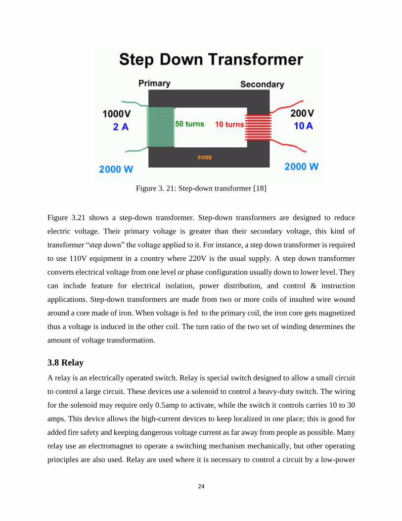
Figure 3.21 shows a step-down transformer. Step-down transformers are designed to reduce
electric voltage. Their primary voltage is greater than their secondary voltage, this kind of
transformer “step down” the voltage applied to it. For instance, a step down transformer is required
to use 110V equipment in a country where 220V is the usual supply. A step down transformer
converts electrical voltage from one level or phase configuration usually down to lower level. They
can include feature for electrical isolation, power distribution, and control & instruction
applications. Step-down transformers are made from two or more coils of insulted wire wound
around a core made of iron. When voltage is fed to the primary coil, the iron core gets magnetized
thus a voltage is induced in the other coil. The turn ratio of the two set of winding determines the
amount of voltage transformation.
3.8 Relay
A relay is an electrically operated switch. Relay is special switch designed to allow a small circuit
to control a large circuit. These devices use a solenoid to control a heavy-duty switch. The wiring
for the solenoid may require only 0.5amp to activate, while the switch it controls carries 10 to 30
amps. This device allows the high-current devices to keep localized in one place; this is good for
added fire safety and keeping dangerous voltage current as far away from people as possible. Many
relay use an electromagnet to operate a switching mechanism mechanically, but other operating
principles are also used. Relay are used where it is necessary to control a circuit by a low-power
25
signal or where several circuits must be controlled by one signal. The first relays were used in long
distance telegraph circuit, repeating the signal coming from one Circuit and re-transmitting it to
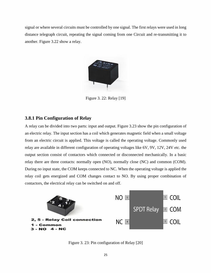
another. Figure 3.22 show a relay.
Figure 3. 22: Relay [19]
3.8.1 Pin Configuration of Relay
A relay can be divided into two parts: input and output. Figure 3.23 show the pin configuration of
an electric relay. The input section has a coil which generates magnetic field when a small voltage
from an electric circuit is applied. This voltage is called the operating voltage. Commonly used
relay are available in different configuration of operating voltages like 6V, 9V, 12V, 24V etc. the
output section consist of contactors which connected or disconnected mechanically. In a basic
relay there are three contacts: normally open (NO), normally close (NC) and common (COM).
During no input state, the COM keeps connected to NC. When the operating voltage is applied the
relay coil gets energized and COM changes contact to NO. By using proper combination of
contactors, the electrical relay can be switched on and off.
Figure 3. 23: Pin configuration of Relay [20]
26
3.8.2 Working principle of Relay
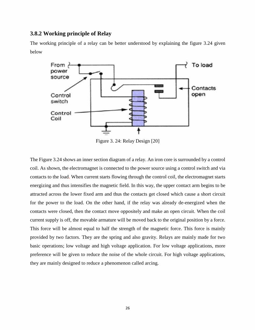
The working principle of a relay can be better understood by explaining the figure 3.24 given
below
Figure 3. 24: Relay Design [20]
The Figure 3.24 shows an inner section diagram of a relay. An iron core is surrounded by a control
coil. As shown, the electromagnet is connected to the power source using a control switch and via
contacts to the load. When current starts flowing through the control coil, the electromagnet starts
energizing and thus intensifies the magnetic field. In this way, the upper contact arm begins to be
attracted across the lower fixed arm and thus the contacts get closed which cause a short circuit
for the power to the load. On the other hand, if the relay was already de-energized when the
contacts were closed, then the contact move oppositely and make an open circuit. When the coil
current supply is off, the movable armature will be moved back to the original position by a force.
This force will be almost equal to half the strength of the magnetic force. This force is mainly
provided by two factors. They are the spring and also gravity. Relays are mainly made for two
basic operations; low voltage and high voltage application. For low voltage applications, more
preference will be given to reduce the noise of the whole circuit. For high voltage applications,
they are mainly designed to reduce a phenomenon called arcing.

27
3.9 Specific work of Transformer, Diode, Capacitor, Zener Diode, Op-amp,
BJT and Relay in the main circuit
o Transformer:
The main power supply of any phase is stepped down by a 120V AC primary to 12V-0-
12V, 300mA secondary step-down transformer to deliver 12V, 300mA which gives the
operating voltage of the op-amp.
o Diode:
The main power supply is stepped down by the transformer to deliver 12V, 300mA, which
is rectified by the diode. The diode chaps of the negative voltage and gives a 12V dc output.
Figure3.25 has shown the diode rectification.
Figure 3. 25: Diode Rectification
o Capacitor:
The capacitor will work as a filter. It will filter the 12V dc output and give smoother 12V
dc output. Figure 3.26 shows capacitor acting as a filter.
Figure 3. 26: Capacitor acting as a filter.

28
o Op-amp:
The 741 op-amp will work as a comparator. It will compare the voltage in pin 2 & pin 3.
The voltage at non-inverting pin 3 of the op-amp is taken from the voltage divider circuit
of resister R1 and preset resister VR1 of the variable resistor. The reference voltage at
inverting pin 2 is fixed to 5.1V through zener diode. Till the supply voltage in one phase is
120V the voltage at non-inverting pin 3 will be higher then 5.1V at the reference voltage
at pin 2, then the output pin 6 will also be high and PNP will remain OFF. If the reference
voltage at pin 2 is higher the voltage at pin 2 then PNP will be ON.
o Zener Diode:
Zener diode is use as a reference voltage which is 5.1V at inverting pin 2. If the reference
voltage on the zener diode will higher than the voltage at pin 3 then PNP will ON.
o BJT:
In the main circuit a PNP transistor is used. If the voltage at non-inverting pin 3 is high
then 5.1V at the reference voltage at pin 2, then the output pin 6 will be high and PNP will
remain OFF. So the relay will remain de-energized, as soon as the reference voltage at pin
2 is higher the voltage at pin 2 then PNP will be ON and the relay will energizes.
o Relay:
If the PNP does not conduct then the relay (RL1) will remain de-energized and phase will
supplies power to the load so relay will remain in normally close (N/C) position. As soon
as PNP is ON then relay (RL1) will energizes and load will be disconnected from phase
and connected to the next phase thorough the next relay (RL2).
3.10. Summary
A very short description of diode, Zener diode, BJT, Op-amp, transformer Relay is given and there
specific work in the circuit is also discussed in this chapter. Those devices are very essential part
of the circuit. Capacitor and Resister are also part of the main circuit but there description is not
given in this chapter. This chapter gives the clear idea of what are the main devices use in the main
circuit and there work.

29
CHAPTER 4
Simulation and Result
4.1 Introduction
Simulating a circuit behavior before actually building it can greatly improve design efficiency by
making faulty designs known as such, and providing insight into the behavior of electronic circuit
design. Our Automatic Phase Changer (APC) circuit has been simulated before implementation to
see how it may operate and what types of fault may occur in practical hardware level. Proteus 8
Professional simulation software is used for simulation here.
4.2 Electronic Simulation Software: Proteus 8 Professional
Proteus is a software for electronic circuit simulation, schematic capture and printed circuit board
(PCB) design. It is developed by Labcenter Electornics. Proteus 8 Professional version has an
enriched component library and many features which help designer to design and analyze a circuit
easily. The figure 4.1 below is shows the design procedure of Automatic Phase Changer circuit in
Proteus. [12]
Figure 4. 1: Wiring the Automatic Phase Changer Circuit in Proteus 8 Professional.

30
4.3 Simulation of the APC circuit
In the simulation three different ac voltage sources of rating Peak Voltage = 120V, Frequency =
60Hz are used as three phase power supply. Doing this allows to increase or decrease the voltage
of any power supply line easily. At the load side three bulbs are used as load for three phase supply.
Fuse of current rating 12A is used in each phase as a protective device. Voltmeters and Ammeters
are used at the places where it is necessary to take the voltage and current for analysis.
As it is described that this circuit works for single and double phase fault or voltage down the
nominal rating at any one or two phases when other phase has correct level of voltage. Therefore,
the simulation has been done under three conditions as follows:
a) All three phases have nominal voltage ratings (120V, 60 Hz)
b) Any one phase has voltage below the nominal rating (<120V, 60 Hz)
c) Any two phases have voltage below the nominal rating (<120V, 60 Hz)
In the all three conditions above loads must get correct level of voltages for their perfect operation.
But at least one supply line must have nominal voltage to supply correct voltage to the others. The
three probable conditions are examined by simulation.
4.3.1 All three phases have nominal voltage ratings (120V, 60 Hz)
When all three power supply lines have correct level of voltage, there is no problem. Then it was
obtained 84.6V (rms value of 120V) in the voltmeter across the loads. The figure 4.2 shows the
current and voltage ratings at the normal condition for one phase. Other two phases have same
ratings as well.

31
Figure 4. 2: Voltage and current rating for phase – 1 (Upper) and voltage across load – 1 (L1, A
bulb) for this phase.
It is seen from the figure 4.2 that in the normal condition each phase carries 3.52A currents for the
load of a bulb of 25W. But practically for various devices current rating may vary. Hence, fuse
12A rated fuses have been used.
4.3.2 Any one phase has voltage below the nominal rating (<120V)
Now it will be observed what happens when any of the power supply lines has voltage less than
the nominal voltage. For example, in the simulation it was made the voltage of phase-3 117V
(<120V). The rms value of 117V is 82.73V, but voltage across the load-3 (L3, A bulb) is still
84.6V which is the rms value of 120V. This implies, the circuit is working properly and load-3 is
getting correct voltage level from the healthy power supply line. Figure 4.3 below shows the
current through phase-3 and voltage across load-3.

32
Figure 4. 3: Current through phase-3 when phase voltage is 117V (Upper). Voltage across load-3
(L3, A bulb) is 84.4V (Rms value of 120V) (Lower).
From the figure 4.3 it is observed that the current through the phase-3 is 0A that means the phase
is disconnected from the load. The load-3 is now getting correct voltage from phase-1. Since phase-
1 is now connected to load-1 as well as load-2 the current through this phase is increased two times
the normal current. So in this condition current through phase-1 is 7.04A (2×3.52A). Figure 4.4
shows this in the simulation below.

33
Figure 4. 4: Current through phase-1 is 7.06A (2×3.52A) because this phase also supplies load-3
as well as load-1.
In this case, it is assumed that phase-3 is faulty. But if phase-1 or phase- 2 gets affected same result
will occur. When phase-1 get affected it gets correct voltage from phase-2 and when phase-2 get
affected it gets correct voltage from phase-3 as we have seen from the main circuit diagram.
4.3.3 Any two phases have voltage below the nominal rating (<120V)
In this section, it will be examined a case where any two phases have voltage below the nominal
rating. Let phase-1 is unaffected and phase-2 & phase-3 have voltage less than 120V (For the
simulation, it was made the affected phase voltage 117V). In this situation since phase-2 and phase-
3 both are affected, phase-1 carries all currents for three loads. So, Current through phase-1 is
10.5A (3×3.52A). It can be observed from the simulation that all three phases have correct level
of voltage under this condition. Therefore, circuit is working properly in simulation. Figure 4.5 to
4.10 show the relevant voltage and current ratings below.

34
Figure 4. 5: Current through phase-2 is 0A and phase-2 voltage (V2) is 117V.
Figure 4. 6: Voltage across load-2 (L2) is 84.3 V (rms value of 120V).

35
Figure 4. 7: Current of phase-3 is 0A and voltage of phase-3 (V3) is 117V.
Figure 4. 8: Voltage across load-3 (L3) is 84.3 V (rms value of 120V).

36
Figure 4. 9: Current through phase-1 is 10.5A and phase-1 voltage (V1) is 120V.
Figure 4. 10: Voltage across load-1 (L1) is 84.4V (Rms value of 120V).

37
4.4 Results of Simulation
The Automatic phase changer circuit may have been observed under three conditions. Results of
each condition are given in table 4.1 below. It was selected 117V as the voltage under the nominal
voltage of 120V because 117V is the maximum voltage for which the circuit considers the supply
line as a faulty line.
Table 4. 1: Results from the simulation for each possible situation.
Situation Phase Voltage (V)
(RMS Voltage)
Current (A) (For
a load of 25W
bulb)
Load voltage
(V) (RMS)
Normal
condition. All the
three phases have
correct ratings.
Phase-1
120 (84.4) 3.52 84.4
Phase-2
120 (84.8) 3.52 84.4
Phase-3
120 (84.8) 3.52 84.4
Phase-3 below
120V
Phase-1
117 (82.7) 0.00 84.4
Phase-2
120 (84.8) 7.05 84.4
Phase-3
120 (84.8) 3.52 84.4
Phase-2 & Phase-
3 below 120V
Phase-1
120 (84.8) 10.5 84.4
Phase-2
117 (82.7) 0.00 84.4
Phase-3 117 (82.7) 0.00 84.4

38
4.5 Summary
From the table 4.1 of simulation result it is observed that when one or two phases have voltage
below 120V the three phase loads always get correct voltages (120V, 84.4V rms) at their terminals
if anyone of three phases is healthy. So, three phase loads or the devices which must be connected
to correct voltage can be connected to three phase lines through this Automatic Phase Changer
circuit. Therefore, it can be said that this simulation is successful.

39
CHAPTER 5
Conclusion and Future Directions
5.1 Limitation of this study
• Currently, this circuit is not workable for over voltage protection.
• During under voltage problem any one of the three phase lines takes the loads of another
on or two lines. If total power of the loads exceeds the power being supplied from that line,
the unnecessary loads needs to be removed from the line. Otherwise voltage may go down
further.
• Therefore, for proper working of this circuit without creating any problem in power system,
it needs to be used three loads of whose total power demand is less than single phase
power capacity.
• This Automatic Phase Changer Circuit works for only emergency loads, which needs
almost nominal voltage to operate.
5.2 Conclusions
The Automatic Phase Changer (APC) is a circuit which changes the phase automatically. Thus it
can find its application in household, hospital and even in industry for emergency loads. From
simulation, the APC circuit has been observed effective and workable. The simulation was done
using Proteus 8 Professional simulation software. Here, it has been used 120V, 60Hz (rms value
is 84.8 V) as rated nominal phase voltage. In the simulation, when peak voltage of any phase falls
down to 117V or less load of that phase was to be connected to next normal phase by the circuit.
The Automatic Phase Changer circuit has some drawbacks as every circuit can have. Otherwise,
it is an applicable circuit for the power system. This circuit further can be improved.

40
5.3 Directions for the future work
This circuit demands future work to improve it. This circuit was made only for under voltage
protection. It can also be implemented for over voltage protection. Microcontroller can be used
instead of Op-amp which will increase the robustness of the circuit. Now, when under voltage
problem occurs only a phase which has normal voltage takes the loads of another one or two phase.
This may arise power overloading problem. In future, there is a scope for automatically shedding
the unnecessary loads from the working line to be included in this project..

41
Appendix A
Datasheet of the Chips used in the circuit

42

43

44

45

46
REFERENCES
1. Khairul A. and Husnain-Al-Bustam (2011), “Power Crisis & Its Solution Through Renewable
Energy in Bangladesh.” Journal of Selected Areas in Renewable and Sustainable Energy”. 1-15
2. Adedokun, G. and Osunpidan, I.B. (2010). Panacea to Epileptic Power Supply in Nigeria. The
Pacific Journal of Science and Technology. 11, 164-170 www.akamaiuniversity.us/PJST.htm.
International Journal of Engineering and Technology Research Vol. 2, No. 4, April 2014, pp. 1 -
15, ISSN: 2327 - 0349 (Online) Available online at www.ijeatr.org
3. Muhammad Ajmal P. “Automatic Phase Changer.”
4. Adedokun, G. and Osunpidan, I.B. (2010). Panacea to Epileptic Power Supply in Nigeria. The
Pacific Journal of Science and Technology. 11, 164-170 www.akamaiuniversity.us/PJST.htm.
International Journal of Engineering and Technology Research Vol. 2, No. 4, April 2014, pp. 1 -
15, ISSN: 2327 - 0349 (Online) Available online at www.ijeatr.org
5. Electronic Devices and Circuit Theory, Robert L. Boylestad and Louis Nashelsky, 10th Edition.
6. Operational Amplifiers and Linear Integrated Circuits, Sixth Edition, Robert F. Coughlin and
Frederick F. Driscoll.
7. Marston, R.M. Diode, transistor & FET circuits manual, Oxford ; Boston : Newnes, 1991
8. Josef Lutz · Heinrich Schlangenotto · Uwe Scheuermann · Rik De Doncker
Semiconductor Power Devices Physics, Characteristics, Reliability
9. Getreu, I.: Modeling the Bipolar Transistor. http://www.lulu.com
10. Bardeen, J., Brattain, W.H.: The transistor, a semi-conductor triode. Phys. Rev. 84(2), 230–
231 (1948)
CrossRef.
11. Marvin Onabajo • Jose Silva-Martinez
Analog Circuit Design for Process Variation-Resilient Systems-on-a-Chip
12. Bennett, Stuart.
A history of control engineering, 1800-1930
IEE control engineering series, 1979

47
13. Koop, Alan Richard.
Fundamentals of relay circuit design, 1965.
14. S. Vlassis and G. Raikos “Bulk-driven differential voltage follower”
ELECTRONICS LETTERS 3rd December 2009 Vol. 45 No. 25
15. Ashfaqur Rahman, Student Member, IEEE, Sajib Roy, Robert Murphree, Student Member,
IEEE, Ramchandra Kotecha, Student Member, IEEE, Kyle Addington, Affan Abbasi, Student
Member, IEEE, Homer A. Mantooth, Fellow, IEEE, Anthony Matt Francis, Member, IEEE, Jim
Holmes, and Jia Di, Senior Member, IEEE
“High-Temperature SiC CMOS Comparator and Op-Amp for Protection Circuits in Voltage
Regulators and Switch-Mode Converters”
IEEE JOURNAL OF EMERGING AND SELECTED TOPICS IN POWER ELECTRONICS,
VOL. 4, NO. 3, SEPTEMBER 2016
16. Heathcote, Martin J, “J and P Transformer Book - A Practical Technology of the Power
Transformer (13th Edition).”
17. McLyman, Wm. T.” Transformer and Inductor Design Handbook (4th Edition),” DATE 2011
18. Bertrand Poulin , Robert M. Del Vecchio , Pierre T. Feghali , Rajendra Ahuja , and Dilipkumar
M. Shah
“Transformer Design Principles,” Chapter 1
19. Anthony F. Sleva.
Protective relay principles, Boca Raton: CRC Press, c2009.
20. Warrington, Albert Russell van Cortlandt.
Protective Relays: their theory and practice, 1968.
Related Documents


![Embeddy_ [1] How to Install Proteus 7](https://static.cupdf.com/doc/110x72/544fb053b1af9f1c168b466f/embeddy-1-how-to-install-proteus-7.jpg)

