This content has been downloaded from IOPscience. Please scroll down to see the full text. Download details: IP Address: 103.27.8.43 This content was downloaded on 24/11/2015 at 15:10 Please note that terms and conditions apply. Design and development of a surface micro-machined push–pull-type true-time-delay phase shifter on an alumina substrate for Ka-band T/R module application View the table of contents for this issue, or go to the journal homepage for more 2012 J. Micromech. Microeng. 22 125006 (http://iopscience.iop.org/0960-1317/22/12/125006) Home Search Collections Journals About Contact us My IOPscience

Welcome message from author
This document is posted to help you gain knowledge. Please leave a comment to let me know what you think about it! Share it to your friends and learn new things together.
Transcript

This content has been downloaded from IOPscience. Please scroll down to see the full text.
Download details:
IP Address: 103.27.8.43
This content was downloaded on 24/11/2015 at 15:10
Please note that terms and conditions apply.
Design and development of a surface micro-machined push–pull-type true-time-delay phase
shifter on an alumina substrate for Ka-band T/R module application
View the table of contents for this issue, or go to the journal homepage for more
2012 J. Micromech. Microeng. 22 125006
(http://iopscience.iop.org/0960-1317/22/12/125006)
Home Search Collections Journals About Contact us My IOPscience
IOP PUBLISHING JOURNAL OF MICROMECHANICS AND MICROENGINEERING
J. Micromech. Microeng. 22 (2012) 125006 (20pp) doi:10.1088/0960-1317/22/12/125006
Design and development of a surfacemicro-machined push–pull-typetrue-time-delay phase shifter on analumina substrate for Ka-band T/Rmodule applicationSukomal Dey and Shiban K Koul
Centre for Applied Research in Electronics (CARE), Indian Institute of Technology Delhi, Hauz Khas,New Delhi 110016, India
E-mail: [email protected]
Received 17 May 2012, in final form 19 September 2012Published 26 October 2012Online at stacks.iop.org/JMM/22/125006
AbstractA radio frequency micro-electro-mechanical system (RF-MEMS) phase shifter based on thedistributed MEMS transmission line (DMTL) concept towards maximum achievable phaseshift with low actuation voltage with good figure of merit (FOM) is presented in this paper.This surface micro-machined analog DMTL phase shifter demonstrates low powerconsumption for implementation in a Ka-band transmit/receive (T/R) module. Thepush–pull-type switch has been designed and optimized with an analytical method andvalidated with simulation, which is the fundamental building block of the design of atrue-time-delay phase shifter. Change in phase has been designed and optimized in push andpull states with reference to the up-state performance of the phase shifter. The workingprinciple of this push–pull-type DMTL phase shifter has been comprehensively worked out. Athorough detail of the design and performance analysis of the phase shifter has been carriedout with various structural parameters using commercially available simulation tools withreference to a change in phase shift and has been verified using a system level simulation. Thephase shifter is fabricated on the alumina substrate, using a suspended gold bridge membranewith a surface micromachining process. Asymmetric behaviour of push–pull bridgeconfiguration has been noted and a corresponding effect on mechanical, electrical and RFperformances has been extensively investigated. It is demonstrated 114◦ dB−1 FOM over0–40 GHz band, which is the highest achievable FOM from a unit cell on an alumina substratereported so far. A complete phase shifter contributes to a continuous differential phase shift of0◦–360◦ over 0–40 GHz band with a minimum actuation voltage of 8.1 V which is the highestachievable phase shift with the lowest actuation voltage as per till date on the aluminasubstrate with good repeatability and return loss better than 11.5 dB over 0–40 GHz band.
(Some figures may appear in colour only in the online journal)
1. Introduction
Development of a radio frequency (RF) micro-electro-mechanical systems (MEMS) phase shifter has greatlyimproved the performance with its low-loss and less-
measurable inter-modulation distortion in phased-arrayradars, satellite communication systems and measurementinstruments. The RF-MEMS phase shifter has been anestablished technology in the transmit–receive (T/R) modulewith a good power-aperture product, and with associated
0960-1317/12/125006+20$33.00 1 © 2012 IOP Publishing Ltd Printed in the UK & the USA
J. Micromech. Microeng. 22 (2012) 125006 S Dey and S K Koul
long-range detection capability for years [1]. It has proved to bean optimal solution in commercial as well as engineering trade-offs with RF-MEMS capacitive switches which demonstrateslow cost, lower parasitic, low power and higher linearitycompared to contemporary solid state devices. Although theswitching speed of MEMS devices may not be comparable tothe FET or p–i–n diode switches, the MEMS devices havebetter performance in terms of isolation and insertion loss atmillimetre-wave frequencies [1]. Utilizing these switches intrue-time-delay (TTD) phase shifters can drastically reduceloss, and thus can significantly reduce the cost and weight fora phased-array antenna where thousands of phase shifters aremounted on the T/R module. TTD refers to the invariance oftime delay with frequency and demonstrates a high-rangeresolution in the form of ultra-wideband radar waveformswithout frequency scanning or beam squinting [2, 3].
A diode loaded transmission line has been used for avariety of applications, both nonlinear [4, 5] and linear [6, 7].In the linear regime, a diode loaded line behaves like asynthetic transmission line where phase velocity changes withapplied voltage and can, therefore, be used as TTD elementsin prototype phased arrays. TTD phase shifters are designedusing the switched-line principle or the distributed loadedline principle. In comparison with the switched line, thedistributed phase shifter gives wideband performance, goodaspect ratio and works well at high frequency. Distributedloaded line TTD phase shifters can be realized analogously ordigitally, and in smaller form factors, which is important in asubarray level. Analog phase shifters are biased with a singlebias line, whereas digital phase shifters require a parallel busalong with complex routing schemes at the subarray level.Devices such as phase arrays often require high isolation inphase control, which often leads to a large and lossy digitalphase shifter system. In addition, using an analog phase shifterin the subarray level avoids large phase quantization errors,which deteriorate the effective isotropically radiated powerand beam-pointing accuracy, and elevate the sidelobe level ofan electronically scanned array [8, 9]. In this work an analogDMTL TTD phase shifter has been chosen for a phased-arrayapplication.
In general, this device consists of a coplanar waveguide(CPW) line that is periodically loaded with MEMS bridges.CPW-based phase shifters are uniplanar as only one side of thesubstrate is used, eliminating the need for a via-hole processand simplifying the fabrication and integration process withother components. When a single analog control bias voltageis applied to the centre conductor, the bridges will be pulledcloser to the centre conductor, which in turn increases theloading capacitance on the distributed line, besides varying thepropagation characteristics and decreasing the phase velocityof the DMTL. The resulting change in the phase velocity ofthe DMTL produces the TTD phase shifts.
Many research groups have endeavoured the subject ofphase shift per decibel noise figure (NF) with better returnloss in the TTD phase shifter. The DMTL design has beendemonstrated from the X- to W-band. Rebeiz [10] was amongthe first who proposed and studied the MEMS distributed phaseshifter. Later, further improvements in the phase shifter were
presented [11–14]. A 1-bit low-loss phase shifter was achievedwith 180◦ at 25 GHz and 270◦ at 35 GHz [11]. In [14], thephase shifter was approximately 240◦ dB−1 at 35 GHz with areturn loss better than 10 dB from 10 to 35 GHz. McFeetors andOkoniewski [15] had presented a DMTL analog phase shifterwith enhanced tuning where 225◦ dB−1 has been achieved at40 GHz. In [16] a DMTL phase shifter has been developedusing a saw-shaped CPW where 20 dB return loss has beenobtained with a 90◦ phase shift at 10 GHz. In [17] a symmetrictoggle MEMS varactor, designed by Rangra et al [18], wasused to obtain a 360◦ phase shift at 35 GHz with a return lossof 15 dB. In [19] an analog slotline TTD had been presentedwith 28.2◦ dB−1 and 59.2◦ cm−1 at 10 GHz. Prior studies havedealt with the structure design of the phase shifters in orderto improve phase shift per decibel NF. However, they havenot been extensive and the dependence of mechanical andelectrical properties on various structural parameters is still anactive area of research. Earlier all these phase shifters reportedso far have experienced high actuation voltage. To achieve highphase shift per decibel NF at high frequency with low actuationvoltage is still an active area of research. Furthermore, for anydevice to be used in a practical application it must be reliableas per life cycle concern.
Phase shift is linearly proportional to the applied bias.To improve the reliability of the TTD phase shifter, it isalways desirable to operate an MEMS bridge within a limitof instability where the electrostatic force becomes equalto restoring force of the MEMS bridge. So, it is alwaysrecommended to actuate an MEMS bridge within a pull-inlimit. To implement the maximum amount of phase shiftwith the minimum amount of insertion loss and the widerbandwidth, the height of the MEMS bridge is always controlledwithin the 2–5 μm range. This leads to high actuation voltage,since the conventional design approach for a phase shift changeis the adjustment of the height of the MEMS bridges. However,the displacement of the bridge’s height is limited for a certainfrequency application and the capacitance ratio (Cr) is small,leading to a small phase shift. In order to increase Cr, aninsulation layer is coated on the centre conductor under thebridges to implement the high capacitance in the down state.In complementary, in order to maintain an acceptable matchingover a wide band, it is recommended not to overload thetransmission line with an excessively large MEMS capacitancein the down state. However, many research groups have usedthe centre conductor as a bottom electrode of the bridge,and to pull the bridge completely down onto the layer onthe dielectric, dielectric charging is required. It can cause theswitch to either remain stuck after the removal of the actuationvoltage or to fail the contact under the application of the pull-in voltage. It degrades the lifetime of the phase shifter as thelifetime is a function of the applied voltage and the contactquality between the bridge and the dielectric. The prior studyof the TTD phase shifter has dealt with the maximum amountof phase shift with the minimum amount of insertion loss withhigh actuation voltage (>25 V). To use this TTD phase shifterin a phased array for the T/R module as shown in figure 1, oneneeds a charge pump. However, charge pumps do not adaptwell to the particularily high load of RF-MEMS for its limited
2

J. Micromech. Microeng. 22 (2012) 125006 S Dey and S K Koul
ΦSPDT SPDT
TX RX
Phase shifter VGA
LNA PA
T/R switch Antenna
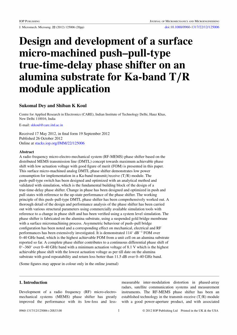
Figure 1. Schematic of the T/R module, where the phase shifter isconnected between two SPDT switches.
slew rates and require longer settling time. Furthermore, thecharge pump has a limited choice for Vout versus Vin and it canbe noisy.
Our work focuses on developing the maximum amountof phase shift with the minimum amount of actuation voltagealong with the improvement on return loss characteristics ofthe TTD phase shifter. Improvement on actuation voltage andswitching time is always an active area of research in MEMSdevices. Switching time is not an important issue in the phaseshifter application if it operates within the pull-in limit. Butlow actuation voltage sometimes affects the device reliability.This work attempts to address these points with a thoroughdetailed analysis of the TTD phase shifter with low actuationvoltage and complete phase shift along with good return losscharacteristics.
In this work, we present the detailed development ofthe MEMS bridge with parametric optimization. Structurallyit is similar to the one in [18, 20]; however, the workingprinciple of this kind of push–pull-type bridge has beencomprehensively worked out which is the fundamentalbuilding block in our TTD phase shifter. A systematicanalytical design methodology has been presented andthe performance evaluation has been carried out on thepush–pull MEMS bridge. The electrostatic-based actuationscheme is used to actuate the MEMS bridge. Completeelectromechanical modelling with parametric optimizationhas been carried out and the theoretical results have beenverified with simulation. The main objective of this work is tomodify the travel range of the overlapping area between theMEMS bridge and the centre conductor. Here, phase shiftingaction has been carried out in three states. These are pull-up, up and pull-down states. A differential phase shift hasbeen obtained with an effective phase difference betweenpull-up and pull-down states. We present a thorough detaileddevelopment of the push–pull-type TTD phase shifter withthe design modelling and complete fabrication process. A Ka-band distributed MEMS phase shifter on a ceramic substratehas been designed, fabricated and tested in this paper. The gold-based surface micromachining process is used to fabricate thisdevice.
The layout of this paper is as follows. The generaloperating principle of the push–pull-type MEMS bridge
followed by the detailed analytical design approach and itsvalidation with the help of simulation have been furnished insection 2. A thorough analytical performance estimation of thephase shifter has been presented in section 3. Details of thefabrication process followed by performance characterizationon the fabricated circuits have been discussed in the subsequentsections.
2. Operating principle: design and simulation
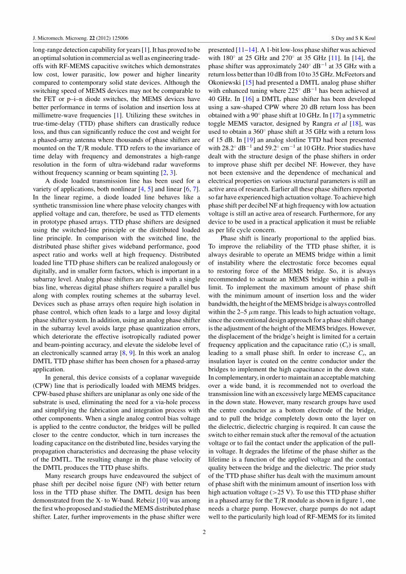
The proposed micro-electro-mechanical push–pull bridgeworks on the principle of electrostatic actuation. The MEMSbridge exploits torsional anchor springs and the third electrodeto mechanically restore the off-state of the bridge in caseof any on-state stiction. There are two fixed electrodes onthe substrate. One is the push electrode and the other is thepull electrode. When this pull voltage is eliminated and pushvoltage is applied, as shown in figure 2(b), the central partis lifted upwards. In the other state, when voltage is appliedto the pull electrode as shown in figure 2(c), the central partof the beam moves down. Such a membrane is composed ofdifferent parts: the central part acting on the mobile plate ofthe variable capacitor, two mobile electrodes implementingthe toggling performance and two levers connected with thecentral parts and mobile electrodes. Actuation is carried outwith the electrostatic torque (Te) and the restoring torque (Tr)with a function of the rotation angle (θ ).
The bridge can be pushed up or down by applying voltageon two couples of fixed electrodes, which are symmetric withrespect to the central transmission line underneath the contactbeam as shown in figure 2(a).
Many researchers had performed a dynamic analysisof this symmetric push–pull bridge. This bridge works ona principle of tortional micro actuator. Plotz et al [21–23]studied on the electrostatic tortional RF-MEMS switch withlow actuation voltage with experimental results, theory andsimulation approaches. The electrostatic tortional mirror isinvestigated from experiment and theory in [24–26]. Hah et al[27] first studied the dynamic analysis of the push–pull bridgewhere actuation was carried out with two tortional springsand one leverage. Rangra [28] had performed a completestructural analysis of this push–pull-type MEMS bridge withfour torsional springs and two leverages and named it thesymmetric toggle switch. Furthermore, Solazzi [29] modifiedand performed a dynamic analysis as per actuation voltageconcern on this symmetric toggle switch. In all these analyses,actuation was carried out with a moment balance equationwith the electrostatic torque (Te) and the restoring torque (Tr)with a function of the rotation angle (θ ). However, above-mentioned research works on the push–pull-type bridge didnot consider the stress, van der Waals (vdW) and Casimireffects due to simplicity of the analysis. In this work, thesimplified two-degree-of-freedom (2DOF) model is appliedto study the actuation mechanism of the push–pull bridgewith the influence of vdW and Casimir torques along withelectrostatic and restoring torques. The influence of torques ona critical tilting angle has been comprehensively worked outto obtain the accurate analytic model of actuation voltage. The
3
J. Micromech. Microeng. 22 (2012) 125006 S Dey and S K Koul
(b)
Push voltage (Vpush)
Pull voltage (Vpull)
(a)
(c)
Fixed electrode
Mobile electrode Contact
beam
Anchor
Torsion spring
Transmission line
θ
θ
fe fvdw
fcas
fcas
fvdw
fvdw fcas
fe fcas fvdw
fR
fR
Vpush
Vpull
Lever
air gap
normal state (Vpush = Vpull = 0)
normal state (Vpush = Vpull = 0)
line of symmetry
line of symmetry
Figure 2. Schematic of (a) top surface of the push–pull-type MEMSbridge. (b) Beam lifted upward due to the push voltage. (c) Beamsnaps down due to the pull voltage. θ defines a rotation angle of thebridge; f cas, f vdw, fe and fR are the Casimir, vdW, electrostatic andrestoring forces, respectively. Dotted line beam indicates the normalstate of the mobile plate under the zero-bias condition.
dynamic study of this electrostatic tortional push–pull bridgehas been subdivided into two sections. In section I, actuationvoltage has been obtained with a quasi-static assumption
where inertia and damping effects are neglected followedby an electromechanical simulation with lumped parametermodelling in the Saber platform. The effects of all torques onactuation voltage under step voltage and modulated voltageresponses have been analytically investigated in section II.
2.1. Section I: quasi-static approximation
The schematic of the push–pull bridge is shown in figure 1. Thecontact of the beam is suspended with two levers physically.The levers are connected with a mobile electrode, which rotatesaround an axis of torsion springs. One end of the torsionspring is anchored with the substrate. There are four fixedelectrodes on the substrate. The rightmost two electrodes arepush electrodes and other two are pull electrodes, as shown infigure 2(a). When voltage is applied to the pull electrodes, acontact beam moves down to make contact with a signal line,as shown in figure 2(c). When this pull voltage is eliminatedand push voltage is applied, as shown in figure 2(b), the contactis lifted upwards. Our objective is to use this bridge in phaseshifting operation where the effective gap height has beenincreased with push voltage (Vpush), and leads to high loadedimpedance. Pull voltage (Vpull) has been applied within thepull-in range.
The analytic model of this 2DOF approximation hasbeen worked out under infinite spring bending stiffness witha pure rotational movement for one half of this symmetricmodel; it is considered only the balance of moments affectingthe membrane rotation with respect to the anchor points.Membrane deflection has been defined in terms of rotation byθ . When the Vpush voltage is applied between the electrodes,an electrostatic attracting force between them will produce anelectrostatic torque (Te), under the action of which the mobileplate will tilt. For a given bias voltage (Vbias), the distributedelectrostatic force (Fe) is
dFe(x)
dx= ε0wme
Vbias
(g0 − θx), (1)
where wme is the mobile electrode width, g0 is the effective gapbetween the mobile electrode and the fixed electrode and x isthe distance from the anchor points according to the referencesystem used in figure 2(a). The following assumption has beensupposed to simplify the analysis:
(i) Residual stress in the mobile plate is ignored.(ii) Error derived from a nonhomogeneous distribution of
charge, after the mobile electrode deflects, is ignored.(iii) Fringing field effect is ignored.(iv) Small deflection is assumed.
The electrostatic torque (Tr) is expressed using a smallangle approximation (lme � g0, sin θ ≈ θ ) in (2) as follows[27]:
Te(θ ) = ε0V 2biaswme
2θ2
⎡⎢⎢⎢⎢⎢⎢⎣
lmeθ
g0−lmeθ+tdεd
+ ln
⎛⎜⎝ g0−lmeθ+
tdεd
g0−(lme−lfe )θ+tdεd
⎞⎟⎠
− (lme−lfe )θ
g0−(lme−lfe )θ+tdεd
⎤⎥⎥⎥⎥⎥⎥⎦
Te(θ ) = ε0V 2biaswme
2θ2(m), (2)
4

J. Micromech. Microeng. 22 (2012) 125006 S Dey and S K Koul
mel
fel
mew
few
ll
tsl
tsw
tst
lw
dt
Figure 3. Three-dimensional model of the push–pull MEMS bridge.
where lme is the mobile electrode length, lfe is the length of thefixed electrode and td and εd are the thickness and dielectricconstant of the insulator, respectively, as shown in figure 3.
When voltage is applied to the push electrodes, theinteraction between the tip of the mobile electrode and thefixed electrode employs a fairly general Lennard–Jones force,whereas McCarthy et al [30] consider a linear spring-likeforce. This new force has an attractive component, called vdWforce (long-range force), and a repulsive component, calledCasimir force (short range force), which has been proved tobe of fundamental importance in MEMS devices [31]. Theseforces allow predicting quickly and with a good approximationthe dynamic response of the system, with bouncing included.Bouncing can introduce severe damage to the mobile electrodeand fixed electrode interface by mechanical hammering andelectrical arching affecting the durability of the system andpossibly leading to the permanent adhesion–stiction [32].
When two plates of a torsional actuator are parallel(θ = 0), the vdW and Casimir forces on the left of the fixed axisequal their counterpart on the right. The resultant torque forceon both sides of the fixed axis is zero. When mobile platestilt with actuation voltage on the push electrode, the vdW andCasimir forces on one side of the fixed axis will not be equalto their counterpart on another side, and the resultant of vdWand Casimir torques is not equal to zero.
When the mobile electrode rotates anti-clockwise an angleθ , the vdW differential forces acting on parallel differentialplates with width wme and infinitesimal length dr on bothsides of the torsional beam are given as follows [33]:
dFLvdW = Awme
6π
dr
(g0 + rθ )3, dFR
vdW = Awme
6π
dr
(g0 + rθ )3,
(3)
where A = π2αρ2 is the Hamarker constant (assumed to be2 × 10−19 J), ρ is the volume density of material and α is theconstant character in the interaction between two atoms.
The torque of these vdW differential forces to the fixedtorsional beam is as follows [33]:
MvdW =∫ lme
0r(dFL
vdW − dFRvdW
)= Awme
12π
1
θ2
[g0 + 2lmeθ
(g0 + lmeθ )2+ −g0 + 2lmeθ
(−g0 + lmeθ )2
]
MvdW = Awme
12πθ2(n). (4)
Casimir torque can be derived as follows [33]:
Mcasimir = π2�cwme
1440
1
θ2
[−g0 + 3lmeθ
(g0 − lmeθ )3+ g0 + 3lmeθ
(g0 + lmeθ )3
]
Mcasimir = π2�cwme
1440θ2(p), (5)
where � is Planck’s constant divided by 2π , which is equalto 1.055 × 10⁻³⁴ J s, and c is the speed of light and equals3 × 108 m s−1.
When the mobile electrodes rotate around the tortionalspring, a restoring torque will be produced due to the elasticrestoring torque of the beam, which can be simplified as aflexure spring with torsional stiffness K.
Restoring moments of the torsional bridge is given by
Mr = MA + MB = MA + FB lfe, (6)
where lfe is the fixed electrode length, MA is the reactionmoment at the anchor under the electric field, and FA and FB
are the reaction forces at the anchors and lever, respectively.Reaction moments at the anchor are given as follows [29]:
MA = 2Ktθ, (7)
where Kt is defined as [29]
Kt = C1E
2(1 − ν)
wtst3ts
lts, (8)
where wts, tts and lts are the width, thickness and length of thetorsional spring, and E and ν are the effective Young modulusand Poisson ratio of membrane material, respectively. Theconstant C1 depends on the wts/tts ratio and it is called thetorsion coefficient. For a rectangular-shaped beam if wts/tts >
10, C1 is equal to 0.33. For wts/tts ≈ 5, C1 is equal to0.25 [29].
The reaction force due to the lever can be demonstratedto be [28]
FB = 2
l2l
EIlθ, (9)
where Il = w3ltl/12;wl , tl and ll are the width, thickness and
length of the lever beam.Rearranging together equations (6)–(9), the spring
stiffness of the beam can be determined as follows [28]:
K = 2
l2l
EIl lfe + 2kt . (10)
In the push–pull-type torsional MEMS actuator, the vdWand Casimir torques are dependent not only on the separationbetween two surfaces but also on the rotation angle. Thedifference of two dimensionless torques exists when theseparation gap is in nanoscale, and the effects of these torquesget larger with a decrement of the gap in the presence of theactuation bias. For a small dimensionless gap, the difference isnot so sensitive to the rotation angle. It is negligible unless therotation angle is large enough. So we will study the influenceof all kinds of torques on the pull-in effect on the push–pull torsional MEMS bridge. From this model, the followingequation of motion can be derived by the classical second-orderlinear differential equation using a small angle approximation,
Iθ + bθ + kθ = Me + MvdW + Mcasimir, (11)
5
J. Micromech. Microeng. 22 (2012) 125006 S Dey and S K Koul
where I is the mass moment of inertia about the centre ofrotation and b is the damping coefficient of the mobile plate.Now using the quasi-static assumption (
..
θ = .
θ = 0), thefollowing moment balance equation describing the voltagerequired for a given equilibrium position is obtained:
Me + MvdW + Mcasimir − kθ = 0. (12)
By comparing equations (2), (4), (5) and (9) with (12), theactuation voltage is obtained as follows:
Vbias =√
2θ3
ε0wme
(K
m
)− S
where S = A
πε0
( n
m
)+ π2
�c
720ε0
( p
m
). (13)
The expressions for m, n and p have been mentioned in(2), (4) and (5), respectively.
The values of constant critical rotation angle and pull-involtage are dependent on the size of the structure. The constantvalue of critical rotation angle has been proved in [29] and thevalue is 0.4404. The critical angle does not remain constant buttends to be constant with the increase of the gap. An effect dueto vdW and Casimir torques on the critical angle is negligible.By numerically calculating the maximum of (13), the point ofinstability (pull-in) is found to be
θ∗ ≈ 0.4404θ0, (14)
where θ0 is the maximum rotation angle (θ0 ≈ g0/lme). Thepull-in voltage (Vpi) associated with this point is obtained as
Vpi =√
0.1708g30
ε0wmel3me
(K
m
)− S
where S = 0.0279A
g0ε0m+ 27.978�c
ε0g20m
. (15)
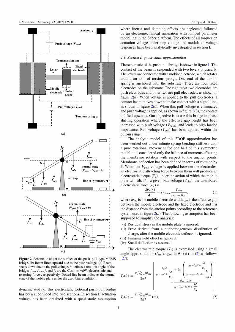
When the bias voltage is small, there exists a solution.However, above a threshold voltage, (15) cannot be solved.It means that the mobile electrode is abruptly pulled downto touch the fixed electrode at the threshold voltage. Figure 4shows the analytic relation between the applied voltage and therotation angle. Here, the maximum Vpush voltage is Vpi; at thisvoltage, the mobile electrode directly touches the rightmostfixed electrode, and the contact beam is lifted upwards. In thiswork, the pull voltage (Vpull) is always lower than Vpush becausethe bridge actuates within the pull-in limit.
The rotation angle θ defines a maximum range (�g) alongout of plane (z-axis) where the mobile plate can move up anddown without incurring in a sudden snap through. In this rangethe moment balance equation (12) is still valid. The maximumdisplacement from the zero-bias position allowed before thesnap through is given as follows [28]:
�g =(
lme + ll3
)g0
lfe. (16)
The initial design parameters and material properties ofthe MEMS push–pull bridge are briefed in tables 1 and 2,respectively. Figure 4 shows the calculated relation betweenthe applied push bias and the rotation angle.
Figure 4. Calculated rotation angle versus the applied push bias.Circle indicates the point of rotation angle after which applied pushvoltage gets almost constant with the increment of rotation angle.
Table 1. Designed dimension of the micro-machined push–pullactuator.
Parameter Value (μm)
Fixed electrode length, lfe 90Fixed electrode width, wfe 230Mobile electrode length, lme 200Mobile electrode width, wme 230Lever length, ll 85Lever width, wl 20Length of the torsional spring, lts 190Width of the torsional spring, wts 15Thickness of the torsional spring, tts 1.25Thickness of lever, tt 1.25
Table 2. Material properties of the push–pull-type MEMS bridge.
Layer for the mobile plate and fixed plate GoldThickness of the layer and the plate, tme 1.25 μmInitial distance between the fixed and 2.5 μmthe mobile electrode, g0
Conductivity of the plate material 4.1 × 10⁷ S m−1a
Density of the plate material, ρ 19 300 kg m−3
Young’s modulus of the plate material, E 45 GPaa
Poisson’s ratio of the plate material, υ 0.41a
Sheet resistance of fixed plate 0.025 /a
Sheet resistance of mobile plate 0.02 /a
Dielectric layer SiO2
Dielectric thickness, td 0.5 μmRelative permittivity of dielectric, εd 4a
aProcess defined.
The primary design of the push–pull bridge has beencarried out analytically using equations (2)–(16). The staticsolution of the equations is used for determining deviceparameters and the dynamic response for the bridge. Thedesign is followed by validation using simulation in the SaberArchitect in the CoventorWare platform [34].
2.1.1. Design validation using simulation. After thedimensions of the beams are obtained from the analytical
6
J. Micromech. Microeng. 22 (2012) 125006 S Dey and S K Koul
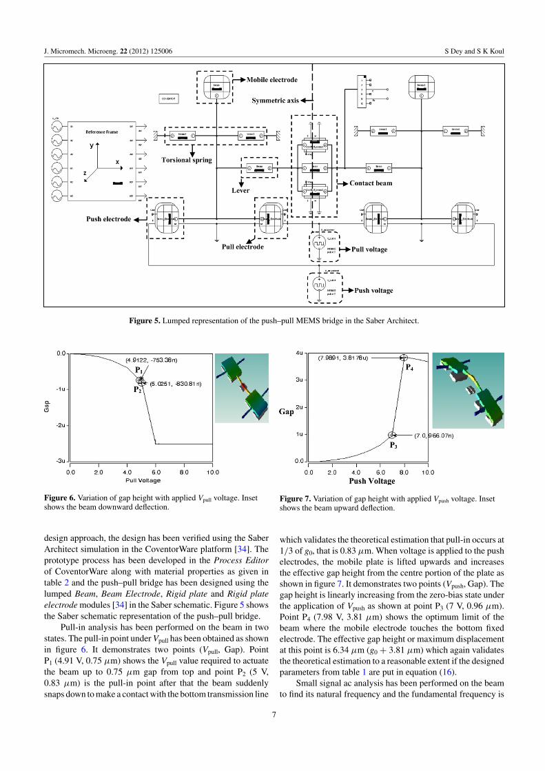
Figure 5. Lumped representation of the push–pull MEMS bridge in the Saber Architect.
Figure 6. Variation of gap height with applied Vpull voltage. Insetshows the beam downward deflection.
design approach, the design has been verified using the SaberArchitect simulation in the CoventorWare platform [34]. Theprototype process has been developed in the Process Editorof CoventorWare along with material properties as given intable 2 and the push–pull bridge has been designed using thelumped Beam, Beam Electrode, Rigid plate and Rigid plateelectrode modules [34] in the Saber schematic. Figure 5 showsthe Saber schematic representation of the push–pull bridge.
Pull-in analysis has been performed on the beam in twostates. The pull-in point under Vpull has been obtained as shownin figure 6. It demonstrates two points (Vpull, Gap). PointP1 (4.91 V, 0.75 μm) shows the Vpull value required to actuatethe beam up to 0.75 μm gap from top and point P2 (5 V,0.83 μm) is the pull-in point after that the beam suddenlysnaps down to make a contact with the bottom transmission line
Figure 7. Variation of gap height with applied Vpush voltage. Insetshows the beam upward deflection.
which validates the theoretical estimation that pull-in occurs at1/3 of g0, that is 0.83 μm. When voltage is applied to the pushelectrodes, the mobile plate is lifted upwards and increasesthe effective gap height from the centre portion of the plate asshown in figure 7. It demonstrates two points (Vpush, Gap). Thegap height is linearly increasing from the zero-bias state underthe application of Vpush as shown at point P3 (7 V, 0.96 μm).Point P4 (7.98 V, 3.81 μm) shows the optimum limit of thebeam where the mobile electrode touches the bottom fixedelectrode. The effective gap height or maximum displacementat this point is 6.34 μm (g0 + 3.81 μm) which again validatesthe theoretical estimation to a reasonable extent if the designedparameters from table 1 are put in equation (16).
Small signal ac analysis has been performed on the beamto find its natural frequency and the fundamental frequency is
7

J. Micromech. Microeng. 22 (2012) 125006 S Dey and S K Koul
Figure 8. Vibration spectrum of the beam. It shows that thefundamental frequency of the beam is 4.86 kHz.
obtained at 4.86 kHz. Figure 8 shows the vibration spectrumof the push–pull bridge.
3. Modelling and optimization of TTD
3.1. Design equation
The model for a TTD unit cell has three operating states, push,up and pull states. In the up state, the model is comprisedof a transmission line of length s, with a capacitor to grounddue to the shunt bridge (Cup) and impedance is Zup. In the pushstate, the central part of the beam is lifted upwards under Vpush,and leads to an increased loaded impedance (Zlpush) with lowcapacitance (Cpush). In the pull state, the bridge moves downwithin the pull-in limit, up to a gap height of 0.75 μm fromthe zero-bias state, and leads to a decreased loaded impedance(Zlpull) with high capacitance (Cpull).
The impedance for each state of the unit cell is given asfollows [10]:
Zup =√√√√ sLt
sCt + CupZpush =
√sLt
sCt + Cpush
Zpull =√
sLt
sCt + Cpull, (17)
where Lt and Ct are the per unit length inductance andcapacitance. These are given as [10]
Ct =√
εeff
cZ0, Lt = CtZ
20 (18)
in which εeff is the effective dielectric constant of thetransmission line, Z0 is the unloaded line impedance and cis the free space velocity.
In order to maintain acceptable matching over a wideband,it is always recommendable not to overload the transmissionline with an excessively large MEMS capacitance. In thiscircuit, a saw-shaped centre conductor is used at the placewhere the MEMS bridge is built to reduce the overlapping
area, which leads to the reduction of down-state impedance asshown in figure 9.
Cpush, Cup and Cpull can be obtained by a parallel plateapproximation, and are given as follows:
Cpush = ε0wcbW1
g1 + tdεr
+ Cf Cup = ε0wcbW1
g0 + tdεr
+ Cf
Cpull = ε0wcbW1
g2 + tdεr
+ Cf . (19)
The TTD phase shifter has a cutoff frequency calledthe Bragg frequency (fB) [7] near the point where almosttotal reflection occurs and impedance becomes zero with nopower transfer. For this reason, the Bragg frequency shouldbe considered carefully to determine the upper operationalfrequency limit.
The Bragg frequency for the unit cell is given as follows[10]:
fB = [π√
sLt (sCt + Cb)]−1, (20)
where Cb is the bridge capacitance. wcb is the width of thecontact beam and Cf is the fringing capacitance which is0.34 times the parallel plate capacitance. g1 is the maximumtravel range when the beam is lifted upwards under Vpush andg2 is the effective gap from top or the zero-bias state, withinthe pull-in range (considered to be 0.75 μm in this work) underVpull.
The spacing (s) and bridge capacitance (Cb) (three states:push, up and pull) of the shunt beam are then calculated byrearranging (17) and given as follows:
s = c(π fB
√εeff
)−1, Cpush = s
[Lt
Z2push
− Ct
],
Cup = s
[Lt
Z2up
− Ct
], Cpull = s
[Lt
Z2pull
− Ct
]. (21)
It is seen from (21) that s is inversely proportional tof B and the εeff of the substrate.
Using (17)–(21), the phase constants in each state (βpush,βpull) and the net phase shift (�φ) are derived as follows:
βpush = 360
2πsω
[√LtCt
(1 + Cpush
Ct
)]
βpull = 360
2πsω
[√LtCt
(1 + Cpull
Ct
)]
�φ = βpush − βpull
= 360
2πsω
[√LtCt
(1 + Cpush
Ct
)]−
√LtCt
(1 + Cpull
Ct
).
(22)
In the push state, the centre beam is lifted upwards sothe phase constant (βpush) decreases due to smaller loadingcapacitance (Cpush), and leads to high loaded impedance(Zpush). The centre beam gets a downward deflection in the pullstate, which leads to higher phase constant (βpull) due to higherloading capacitance (Cpull) with low loaded impedance (Zpull).
8

J. Micromech. Microeng. 22 (2012) 125006 S Dey and S K Koul
Figure 9. Layout of complete TTD phase shifter. Inset shows the saw-shaped CPW. Complete area of the phase shifter is 8.5 mm2.
Therefore, the difference in phase constants (�φ) between thetwo states increases.
The total travel range (TTR) of the push–pull TTD phaseshifter is given as follows:
TTR (μm) = g1 + g2 = 3.81 + 0.75 = 4.56. (23)
The capacitance ratio (Cr) of the push–pull-type MEMSbridge is given as follows:
Cr = Cpull
Cpush. (24)
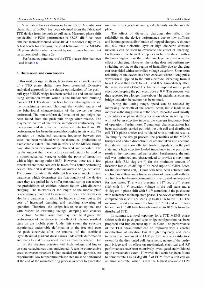
The first phase of our work focuses on the developmentof a unit cell of the phase shifter. The second phase dealswith the repetition of the unit cell with a constant spacing tomake a complete TTD phase shifter. The layout of the DMTLTTD phase shifter has been made in the CoventorWare layouteditor platform where 11 unit cells are periodically placed witha 780 μm spacing as shown in figure 10.
4. Fabrication
The process of push–pull TTD phase shifter starts with a0.025′′ thick alumina substrate polished on both sides. Therelative permittivity of the substrate is 9.8 with a loss tangentof 0.0001 at 1 MHz. The masks that are used for the process areE-beam-write chrome masks. The alumina substrate is used inthis work because of its following properties:
(1) Good mechanical strength(2) Good heat conductivity and fire resistance(3) Good corrosion and wear resistance(4) Very good electric insulation(5) Good surface with high smoothness and less porosity(6) Stable in very high temperature and corrosive chemical.
The characteristic of substrate materials (Al2O3) is givenin table 3.
The fabrication process requires six masks and consistsof the following steps as shown in figure 10.
Step 1. After the RCA cleaning of the wafer, the first layerof chromium (Cr) is deposited and patterned using the lift-offtechnique. This layer is used to make electrical biasing in thecircuit by mask 1.
Step 2. A 0.3 μm of silicon oxide (SiO2) is deposited usingplasma enhanced chemical vapour deposition (PECVD) andpatterned. RIE is employed to pattern the oxide and removethe patterning of photo-resists. This is a passivation layer anddeposited on the last layer (Cr) by mask 2. The sheet resistanceof this layer is 0.025 /sq.
Step 3. An evaporated 400 A chromium/100 nm goldbilayer is deposited as a seed layer. A photo-resist mould Figure 10. Schematic view of micro-fabrication process steps.
9
J. Micromech. Microeng. 22 (2012) 125006 S Dey and S K Koul
(a) (b) (c)
(d) (e) (f )
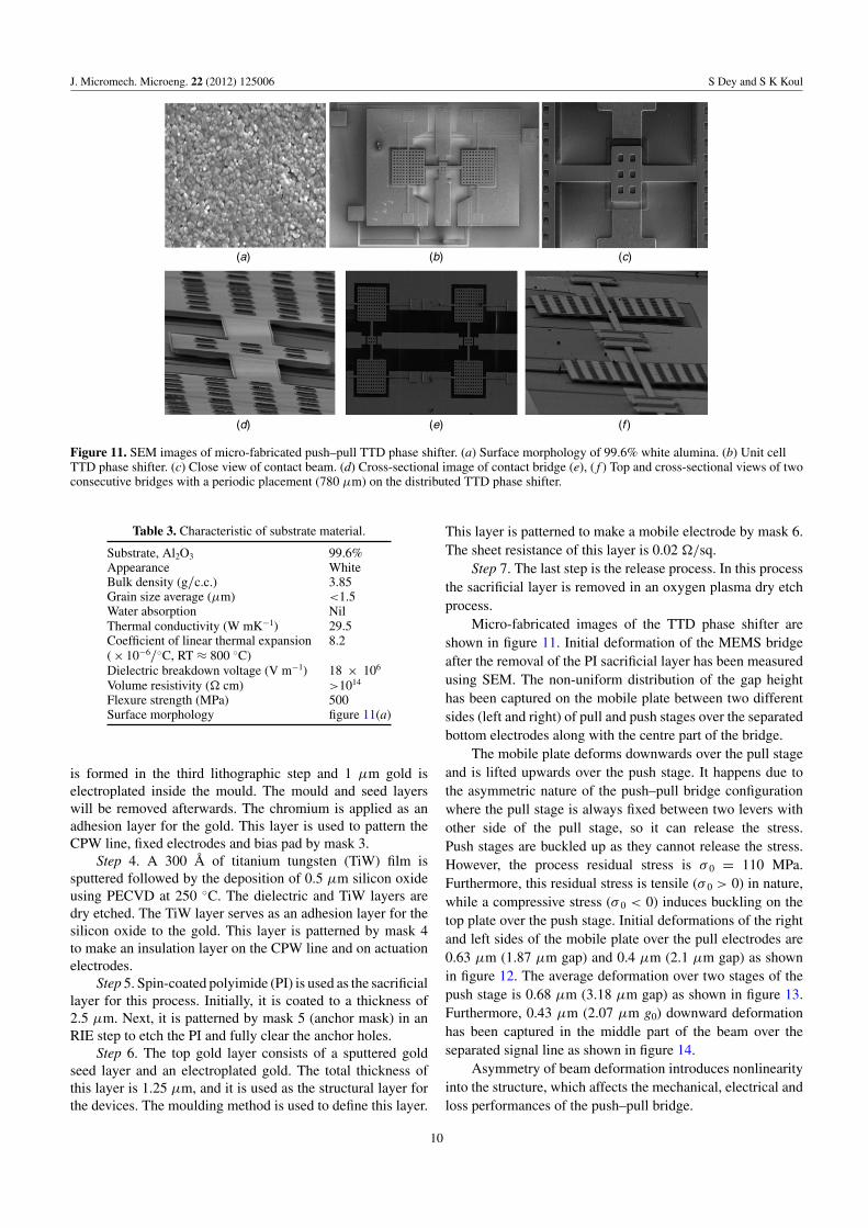
Figure 11. SEM images of micro-fabricated push–pull TTD phase shifter. (a) Surface morphology of 99.6% white alumina. (b) Unit cellTTD phase shifter. (c) Close view of contact beam. (d) Cross-sectional image of contact bridge (e), ( f ) Top and cross-sectional views of twoconsecutive bridges with a periodic placement (780 μm) on the distributed TTD phase shifter.
Table 3. Characteristic of substrate material.
Substrate, Al2O3 99.6%Appearance WhiteBulk density (g/c.c.) 3.85Grain size average (μm) <1.5Water absorption NilThermal conductivity (W mK−1) 29.5Coefficient of linear thermal expansion 8.2( × 10−6/◦C, RT ≈ 800 ◦C)Dielectric breakdown voltage (V m−1) 18 × 106
Volume resistivity ( cm) >1014
Flexure strength (MPa) 500Surface morphology figure 11(a)
is formed in the third lithographic step and 1 μm gold iselectroplated inside the mould. The mould and seed layerswill be removed afterwards. The chromium is applied as anadhesion layer for the gold. This layer is used to pattern theCPW line, fixed electrodes and bias pad by mask 3.
Step 4. A 300 A of titanium tungsten (TiW) film issputtered followed by the deposition of 0.5 μm silicon oxideusing PECVD at 250 ◦C. The dielectric and TiW layers aredry etched. The TiW layer serves as an adhesion layer for thesilicon oxide to the gold. This layer is patterned by mask 4to make an insulation layer on the CPW line and on actuationelectrodes.
Step 5. Spin-coated polyimide (PI) is used as the sacrificiallayer for this process. Initially, it is coated to a thickness of2.5 μm. Next, it is patterned by mask 5 (anchor mask) in anRIE step to etch the PI and fully clear the anchor holes.
Step 6. The top gold layer consists of a sputtered goldseed layer and an electroplated gold. The total thickness ofthis layer is 1.25 μm, and it is used as the structural layer forthe devices. The moulding method is used to define this layer.
This layer is patterned to make a mobile electrode by mask 6.The sheet resistance of this layer is 0.02 /sq.
Step 7. The last step is the release process. In this processthe sacrificial layer is removed in an oxygen plasma dry etchprocess.
Micro-fabricated images of the TTD phase shifter areshown in figure 11. Initial deformation of the MEMS bridgeafter the removal of the PI sacrificial layer has been measuredusing SEM. The non-uniform distribution of the gap heighthas been captured on the mobile plate between two differentsides (left and right) of pull and push stages over the separatedbottom electrodes along with the centre part of the bridge.
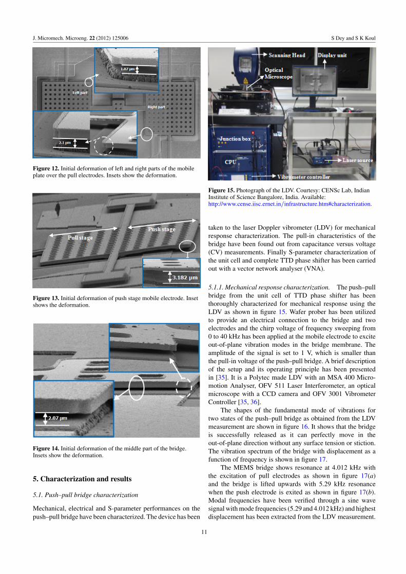
The mobile plate deforms downwards over the pull stageand is lifted upwards over the push stage. It happens due tothe asymmetric nature of the push–pull bridge configurationwhere the pull stage is always fixed between two levers withother side of the pull stage, so it can release the stress.Push stages are buckled up as they cannot release the stress.However, the process residual stress is σ 0 = 110 MPa.Furthermore, this residual stress is tensile (σ 0 > 0) in nature,while a compressive stress (σ 0 < 0) induces buckling on thetop plate over the push stage. Initial deformations of the rightand left sides of the mobile plate over the pull electrodes are0.63 μm (1.87 μm gap) and 0.4 μm (2.1 μm gap) as shownin figure 12. The average deformation over two stages of thepush stage is 0.68 μm (3.18 μm gap) as shown in figure 13.Furthermore, 0.43 μm (2.07 μm g0) downward deformationhas been captured in the middle part of the beam over theseparated signal line as shown in figure 14.
Asymmetry of beam deformation introduces nonlinearityinto the structure, which affects the mechanical, electrical andloss performances of the push–pull bridge.
10
J. Micromech. Microeng. 22 (2012) 125006 S Dey and S K Koul
Figure 12. Initial deformation of left and right parts of the mobileplate over the pull electrodes. Insets show the deformation.
Figure 13. Initial deformation of push stage mobile electrode. Insetshows the deformation.
Figure 14. Initial deformation of the middle part of the bridge.Insets show the deformation.
5. Characterization and results
5.1. Push–pull bridge characterization
Mechanical, electrical and S-parameter performances on thepush–pull bridge have been characterized. The device has been
Figure 15. Photograph of the LDV. Courtesy: CENSc Lab, IndianInstitute of Science Bangalore, India. Available:http://www.cense.iisc.ernet.in/infrastructure.htm#characterization.
taken to the laser Doppler vibrometer (LDV) for mechanicalresponse characterization. The pull-in characteristics of thebridge have been found out from capacitance versus voltage(CV) measurements. Finally S-parameter characterization ofthe unit cell and complete TTD phase shifter has been carriedout with a vector network analyser (VNA).
5.1.1. Mechanical response characterization. The push–pullbridge from the unit cell of TTD phase shifter has beenthoroughly characterized for mechanical response using theLDV as shown in figure 15. Wafer prober has been utilizedto provide an electrical connection to the bridge and twoelectrodes and the chirp voltage of frequency sweeping from0 to 40 kHz has been applied at the mobile electrode to exciteout-of-plane vibration modes in the bridge membrane. Theamplitude of the signal is set to 1 V, which is smaller thanthe pull-in voltage of the push–pull bridge. A brief descriptionof the setup and its operating principle has been presentedin [35]. It is a Polytec made LDV with an MSA 400 Micro-motion Analyser, OFV 511 Laser Interferometer, an opticalmicroscope with a CCD camera and OFV 3001 VibrometerController [35, 36].
The shapes of the fundamental mode of vibrations fortwo states of the push–pull bridge as obtained from the LDVmeasurement are shown in figure 16. It shows that the bridgeis successfully released as it can perfectly move in theout-of-plane direction without any surface tension or stiction.The vibration spectrum of the bridge with displacement as afunction of frequency is shown in figure 17.
The MEMS bridge shows resonance at 4.012 kHz withthe excitation of pull electrodes as shown in figure 17(a)and the bridge is lifted upwards with 5.29 kHz resonancewhen the push electrode is exited as shown in figure 17(b).Modal frequencies have been verified through a sine wavesignal with mode frequencies (5.29 and 4.012 kHz) and highestdisplacement has been extracted from the LDV measurement.
11

J. Micromech. Microeng. 22 (2012) 125006 S Dey and S K Koul
(a)
(b)
Figure 16. Snapshot of the fundamental mode of vibration of thebeam in two states. It clearly shows that the beam end freely movesin the out-of-plane direction under the actuation of (a) pushelectrodes and (b) pull electrodes.
It ensures about the first mode of vibration of the push–pullbridge. Mode 2 has been observed at 31 kHz from both thestates as shown in figure 17.
The difference in the resonance frequencies between pushand pull states is due to stretching of the lever length underexcitation. In the push–pull bridge, the gap height is larger thanthe bridge thickness (tb), so that the maximum deflection at themiddle point is larger than tb, considering the invalidity of asmall deflection. In the push stage, the beam moves up withthe elongation of the effective length of the leverage due to anelectrostatic effect, which leads to an increase in the effectivespring constant (KeffPush) in the overall structure. It introducesless damping and shifts the resonance frequency ( f 0 Push) at ahigher level. On the other hand in the pull state, the centralpart of the beam bends down with negligible increment of theeffective spring constant (KeffPull) with high damping and leadsto a decrease of resonance frequency ( f 0 Pull).
The effect of stress also influences the variation ofresonance frequencies in the design of the push–pull bridge dueto the stress-stiffening effect. The structure bends downwardswith tensile stress and bends upwards with compressive stress.The structure exhibits an out-of-plane instability, since the
(a)
(b)
Figure 17. Vibration spectrum of the push–pull bridge. (a) Pull state shows a resonance at 4.012 kHz. (b) Push state shows a resonance peakat 5.29 kHz.
12

J. Micromech. Microeng. 22 (2012) 125006 S Dey and S K Koul
Table 4. Mechanical performance of the push–pull bridge.
Parameter Value
Push state resonance, f 0 5.29 kHzPull state resonance, f 0 4.01 kHzPush states f max and f -3dB 5.76 and 4.114 kHzPull states f max and f -3dB 4.28 and 3.97 kHzPush state Q factor 1.4Pull state Q factor 1.07
thickness of the suspended structure is much less than the otherdimensions. A compressive stress induces buckling in the topplate (figure 13) over the push electrode when the stress higherthan the critical stress (Euler buckling criterion) leads to theeffect on the overall effective spring constant of the structurewith a non-uniform force profile, which deviates the resonancefrequency with beam stretching. Under excitation, nonlinearityof the electrostatic attraction force causes a variation of thefundamental natural frequency of the structure between thetwo states due to the effect of spring softening. KeffPush andKeffPull between the two states have been found to be 8.305and 6.589 N m−1, respectively. The quality factor of thepush–pull bridge has been obtained from the measuredvibration spectrum of figure 17 for both the states. Themaximum frequency ( f max) and −3 dB frequency ( f −3dB)values have been captured with both states from the vibrationspectrum of LDV measurement as shown in figure 17. Thequality factor (Q) can be expressed as
Q = fmax
f−3dB. (25)
The mechanical performance of the push–pull bridge issummarized in table 4.
Spring softening and damping influence the variation ofresonance frequency between the two states which has beenproved up to a reasonable limit by equations (26)–(29). Themeasured quality factors at push (Qpush) and pull (Qpull) stagesare 1.4 and 1.07, respectively (table 4). So, the overall dampingcoefficient (b) can be estimated as follows:
b = 1
2Q. (26)
The natural frequency (fn) of the structure between the twostates can be found from the measured resonance frequencies( f o) and b, given by the formula
fn = f0√1 − 2b2
. (27)
Furthermore the natural frequency of the structure can bedefined as
fn =√
Keff
m, (28)
where m is assumed to be constant throughout the analysis.By equating equations (27) and (28), the condition for
resonance frequency deviation between the push and pull stateshas been derived and shown as follows:√
KeffPush
Keffpull=
(f0 Push
f0 Pull
)√1 − 2b2
Pull
1 − 2b2Push
, (29)
Figure 18. Snapshot of one mode of vibration under the in-planeand out-of-plane bending motion. Inset shows the lateral motion ofspring.
Table 5. Effecting parameter for a resonance frequency deviation.
Parameter Value
Push state damping coefficient, bpush 0.357Pull state damping coefficient, bpull 0.467Push state spring constant (KeffPush) 8.305 N m−1
Pull state spring constant (KeffPush) 6.589 N m−1
where bpull and bpush are the damping at the pull and pushstages. To validate equation (29), all effecting parameters havebeen listed in table 5.
Using the parameters listed in tables 4 and 5, the right-and left-hand sides of equation (29) are found to be 1.122and 1.147, which validates the prior assumptions of frequencydeviation with 2.1% tolerance. The limit of tolerance isquite reasonable as the test condition includes unavoidableenvironmental perturbations, damping and mobile plate non-uniformities which are difficult to consider in the simulationof the effective spring constant (Keff) using the HarmonicEManalysis in the Coventor ware software platform.
Deflection of the beam occurs due to the torsional motionof four springs as one part of the structure (either push orpull) gets actuated at a time. Due to the twisting nature ofthe beam, the structure deflects vertically with out-of-planebending motion under excitation which has been extractedfrom LDV and at the same instant a horizontal part of the beamdeflection is also introduced at the same resonance frequency,causing in-plane bending motion in the overall structure.
Deflection of the beam is not always necessary due to onlyelectrostatic attraction force between the push or pull electrodeand mobile plate; the fringing field can attract any other partof the beam, which leads to a lateral motion. So, the push–pull bridge configuration undergoes in-plane and out-of-planebending motion under excitation at the same mode frequency.In-plane bending motion has been observed at the part of thetortional springs which is connected to the mobile plate andout-of-plane bending motion occurs at the central part of thebridge as shown in figure 18.
5.1.2. Electrical characterization. Electrical characteriza-tion of the push–pull bridge has been carried out using anAgilent 4284A LCR meter with a probe station [37]. Figure 19
13

J. Micromech. Microeng. 22 (2012) 125006 S Dey and S K Koul
Figure 19. Photograph of the Agilent 4284A LCR meter with theprobe station. The probe station (inset), interfacing computer, LCRmeter and the probes are marked. Probe station is kept in the shutter.Display unit is not shown. Courtesy: CENSc Lab, Indian Institute ofScience Bangalore, India. Available:http://www.cense.iisc.ernet.in/infrastructure.htm#characterization.
shows the photograph of the setup used for characterizing theswitch. It contains a display unit and the probe station alongwith the LCR meter. The pull-in effect of the structure hasbeen performed using a dc probe station manufactured bySus-Microtec. Characterization has been carried out with twostates: push and pull states.
Effect on the pull stage. To measure the C–V characteristicsfor the pull state, the bottom fixed electrodes have beengrounded and the required voltage sweep from 0 to 10 V hasbeen applied to the top suspended or mobile electrode using theprobes. A small ac signal of 5 MHz has been imposed on thedc actuation voltage to measure the capacitance. Open circuitoffset measurement corrections were made before recordingthe capacitance values.
Three steps of capacitance variation have been observedin the pull state as shown in figure 20. Initial deformation ofthe mobile plate introduces asymmetry on the bridge actuationover the separated bottom electrodes. It has been observed thatinitial deformation of the mobile electrode with respect to thebottom fixed pull electrode is not equal between two stages.Downward deformation on the left part of the mobile plateover the pull electrode is more compared to the other side asshown in figure 12.
Capacitance variation on the left side of the pull electrodeis more compared to the other part at the same voltageexcitation for the asymmetric gap height. Due to this, asudden change in capacitance variation has been observedwith a voltage variation from 2 to 2.1 V as shown instep 1, figure 20. The bridge reaches the point of instabilitywith voltage variation from 4.2 to 4.4 V and after that (>4.5 V)it completely snaps down as shown in step 2. The non-uniformdistribution of the gap height over the mobile plate along withthe effect of stress-stiffing leads to two-step pull-in as defined
Figure 20. CV variations under the pull state.
by steps 2 and 3. The non-uniformity may depend on thedifferent positions of the dielectric–membrane contact points,and on the non-uniformity of the dielectric–membrane gap.One explanation of this voltage shift would be the effect ofdielectric charging during step 3, as the bottom electrode isinsulated with dielectric. Due to the high electric field, thelaterally inhomogeneous distribution of charge can be injectedin the dielectric. The trap charges change the electric field andlead to shift the C–V curve to step 3 with a built-in voltage.This built-in voltage is proportional to the amount of charge,and to the distance between the trapped charge and the fixedbottom pull electrodes. The primary effect of such a trappedcharge is to shift the whole C–V characteristic towards positiveof the voltage axis due to negative charge induction into thedielectric layer. However, there is another possible explanationof shifting the C–V curve from step 2 to step 3 which is thereduction of the gap due to the mechanical degradation of thesprings when the bridge is stressed. So, the narrowing effectof the C–V curve at step 3 can be avoided with controlledactuation voltage up to the point of instability (<4.4 V).
Effect on the push stage. In the push state, the mobileelectrode moves up with the applied bias. It has been observedthat the mobile plate is lifted up 0.68 μm from the initialgap height (2.5 μm) over the push electrode (figure 13). Avoltage sweep from 0 to 17 V has been imposed on the mobileelectrode with reference to the fixed ground electrodes. Anotable decrement of capacitance has been captured throughthe LCR meter, as the effective gap height is increased withthe applied dc bias.
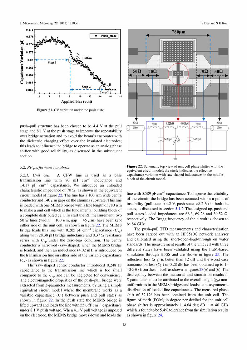
The non-uniform profile of the beam introduces a veryslow change in capacitance variation with a voltage variationup to 8.1 V, as shown in step 1, figure 21. Once it reaches 8.2 V(point A), the beam encounters with the point of instabilitywith a sudden decrement of capacitance (step 2). The bridgemoves up completely (point B) with 15 V of the actuationbias followed by constant capacitance variation up to 17 Vas shown in figure 21. The point of instability (pull-in) of the
14
J. Micromech. Microeng. 22 (2012) 125006 S Dey and S K Koul
Figure 21. CV variation under the push state.
push–pull structure has been chosen to be 4.4 V at the pullstage and 8.1 V at the push stage to improve the repeatabilityover bridge actuation and to avoid the beam’s encounter withthe dielectric charging effect over the insulated electrodes;this leads to influence the bridge to operate as an analog phaseshifter with good reliability, as discussed in the subsequentsection.
5.2. RF performance analysis
5.2.1. Unit cell. A CPW line is used as a basetransmission line with 70 nH cm−1 inductance and14.17 pF cm−1 capacitance. We introduce an unloadedcharacteristic impedance of 70 , as shown in the equivalentcircuit model of figure 22. The line has a 100 μm wide centreconductor and 140 μm gaps on the alumina substrate. This lineis loaded with one MEMS bridge with a line length of 780 μmto make a unit cell which is the fundamental building block ofa complete distributed cell. To start the RF measurement, two50 lines (width = 100 μm, gap = 45 μm) have been kepteither side of the unit cell, as shown in figure 22. The MEMSbridge loads this line with 0.205 pF cm−1 capacitance (Cup)along with 28.38 pH bridge inductance and 0.37 resistanceseries with Cup under the zero-bias condition. The centreconductor is narrowed (saw-shaped) when the MEMS bridgeis loaded, and then an inductance (4.02 nH) is introduced onthe transmission line on either side of the variable capacitance(Cr) as shown in figure 22.
The saw-shaped centre conductor introduced 0.248 fFcapacitance to the transmission line which is too smallcompared to the Cup and can be neglected for convenience.The electromagnetic properties of the push–pull bridge wereextracted from S-parameter measurements, by using a simpleequivalent circuit model where the membrane works as avariable capacitance (Cr) between push and pull states asshown in figure 22. In the push state the MEMS bridge islifted upward and loads the line with 55.6 fF cm−1 capacitanceunder 8.1 V push voltage. When 4.1 V pull voltage is imposedon the electrode, the MEMS bridge moves down and loads the
Figure 22. Schematic top view of unit cell phase shifter with theequivalent circuit model; the circle indicates the effectivecapacitance variation with saw-shaped inductances in the middleblock of the circuit model.
line with 0.589 pF cm−1 capacitance. To improve the reliabilityof the circuit, the bridge has been actuated within a point ofinstability (pull state <4.2 V, push state <8.2 V) in both thestates, as discussed in section 5.1.2. The designed up, push andpull states loaded impedances are 66.3, 69.28 and 39.52 ,respectively. The Bragg frequency of the circuit is chosen tobe 84 GHz.
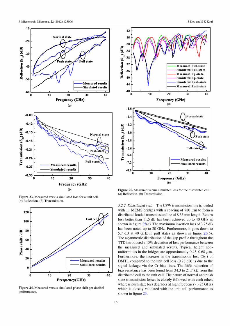
The push–pull TTD measurements and characterizationhave been carried out with an HP8510C network analyserand calibrated using the short-open-load-through on waferstandards. The measurement results of the unit cell with threedifferent states have been validated using the FEM-basedsimulation through HFSS and are shown in figure 23. Thereflection loss (S11) is better than 12 dB and the worst casetransmission loss (S21) of 0.28 dB has been obtained up to 1–40 GHz from the unit cell as shown in figures 23(a) and (b). Thediscrepancy between the measured and simulation results inS-parameters must be attributed to the overall height (g0) non-uniformities in the MEMS bridges and leads to the asymmetricdistribution of loaded line capacitances. The measured phaseshift of 32.12◦ has been obtained from the unit cell. Thefigure of merit (FOM) in degree per decibel for the unit cellphase shifter is approximately 114.64 deg dB−1 at 40 GHzwhich is found to be 5.4% tolerance from the simulation resultsas shown in figure 24.
15
J. Micromech. Microeng. 22 (2012) 125006 S Dey and S K Koul
(a)
(b)
Figure 23. Measured versus simulated loss for a unit cell.(a) Reflection, (b) Transmission.
Figure 24. Measured versus simulated phase shift per decibelperformance.
(a)
(b)
Figure 25. Measured versus simulated loss for the distributed cell.(a) Reflection. (b) Transmission.
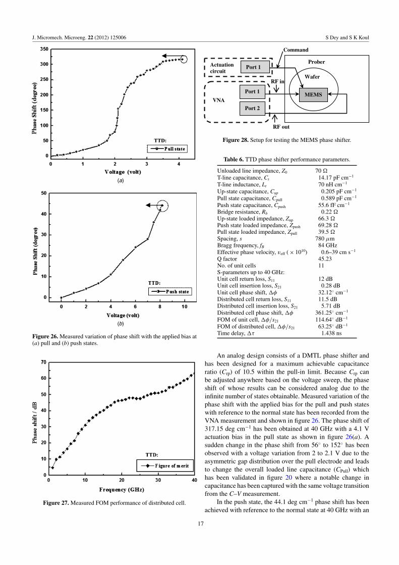
5.2.2. Distributed cell. The CPW transmission line is loadedwith 11 MEMS bridges with a spacing of 780 μm to form adistributed loaded transmission line of 8.35 mm length. Returnloss better than 11.5 dB has been achieved up to 40 GHz asshown in figure 25(a). The maximum insertion loss of 3.75 dBhas been noted up to 20 GHz. Furthermore, it goes down to5.7 dB at 40 GHz in pull states as shown in figure 25(b).The asymmetric distribution of the gap profile throughout theTTD introduced a 15% deviation of loss performance betweenthe measured and simulated results. Typical height non-uniformities in the bridges are approximately 0.43–0.68 μm.Furthermore, the increase in the transmission loss (S21) ofDMTL compared to the unit cell loss (0.28 dB) is due to thesignal leakage via the Cr bias lines. The 36% reduction ofbias resistance has been found from 34.3 to 21.7 k from thedistributed cell to the unit cell. The nature of normal and pushstate transmission losses is closely followed with each other,whereas push state loss degrades at high frequency (>25 GHz)which is closely validated with the unit cell performance asshown in figure 23.
16
J. Micromech. Microeng. 22 (2012) 125006 S Dey and S K Koul
(a)
(b)
Figure 26. Measured variation of phase shift with the applied bias at(a) pull and (b) push states.
Figure 27. Measured FOM performance of distributed cell.
MEMS
Wafer
Actuation circuit
Port 1
Port 1
Port 2 VNA
RF in
RF out
Prober
Command
Figure 28. Setup for testing the MEMS phase shifter.
Table 6. TTD phase shifter performance parameters.
Unloaded line impedance, Z0 70
T-line capacitance, Ct 14.17 pF cm−1
T-line inductance, Lt 70 nH cm−1
Up-state capacitance, Cup 0.205 pF cm−1
Pull state capacitance, Cpull 0.589 pF cm−1
Push state capacitance, Cpush 55.6 fF cm−1
Bridge resistance, Rb 0.22 Up-state loaded impedance, Zup 66.3 Push state loaded impedance, Zpush 69.28 Pull state loaded impedance, Zpull 39.5 Spacing, s 780 μmBragg frequency, fB 84 GHzEffective phase velocity, veff ( × 1010) 0.6–39 cm s−1
Q factor 45.23No. of unit cells 11S-parameters up to 40 GHz:Unit cell return loss, S11 12 dBUnit cell insertion loss, S21 0.28 dBUnit cell phase shift, �φ 32.12◦ cm−1
Distributed cell return loss, S11 11.5 dBDistributed cell insertion loss, S21 5.71 dBDistributed cell phase shift, �φ 361.25◦ cm−1
FOM of unit cell, �φ/s21 114.64◦ dB−1
FOM of distributed cell, �φ/s21 63.25◦ dB−1
Time delay, �τ 1.438 ns
An analog design consists of a DMTL phase shifter andhas been designed for a maximum achievable capacitanceratio (Crp) of 10.5 within the pull-in limit. Because Crp canbe adjusted anywhere based on the voltage sweep, the phaseshift of whose results can be considered analog due to theinfinite number of states obtainable. Measured variation of thephase shift with the applied bias for the pull and push stateswith reference to the normal state has been recorded from theVNA measurement and shown in figure 26. The phase shift of317.15 deg cm−1 has been obtained at 40 GHz with a 4.1 Vactuation bias in the pull state as shown in figure 26(a). Asudden change in the phase shift from 56◦ to 152◦ has beenobserved with a voltage variation from 2 to 2.1 V due to theasymmetric gap distribution over the pull electrode and leadsto change the overall loaded line capacitance (CPull) whichhas been validated in figure 20 where a notable change incapacitance has been captured with the same voltage transitionfrom the C–V measurement.
In the push state, the 44.1 deg cm−1 phase shift has beenachieved with reference to the normal state at 40 GHz with an
17
J. Micromech. Microeng. 22 (2012) 125006 S Dey and S K Koul
8.1 V actuation bias as shown in figure 26(b). A continuousphase shift of 0–360◦ has been obtained from the fabricatedTTD device from the push to pull state. Measured phase shiftper decibel or FOM performance of 63.25◦ dB−1 has beenobtained from distributed cell at 40 GHz as shown in figure 27.A test bench for verifying the joint behaviour of the MEMS-RF phase shifters when actuated by our circuits has been setup as described in figure 28.
Performance parameters of the TTD phase shifter has beenlisted in table 6.
6. Discussion and conclusions
In this work, design, analysis, fabrication and characterizationof a TTD phase shifter have been presented. Extensiveanalytical approach for the design optimization of the push–pull-type MEMS bridge has been carried out and consolidatedusing simulation results which is the fundamental bulidingblock of TTD. The device has been fabricated using the surfacemicromachining process. Thorough the detailed analysis ofthe behavioural characterization of the device has beenperformed. The non-uniform deformation of gap height hasbeen found from the push–pull bridge after release. Theassymetric nature of the device introduced nonlinearity intothe system, and its effect on mechanical, electrical and RFperformances has been discussed thoroughly in this work. Thedeviation on mechanical resonance frequency between twostates has been validated with the theoretical predictions toa reasonable extent. The pull-in effects of the MEMS bridgehave also been experimentally observed and reported. Theresults suggest that the structure can indubitably be used asa micromechanical varactor within the point of instabilitywith a high tuning ratio (10.5). However, there are a fewaspects where more care can be taken for a better performingdevice. The first is definitely the assymetric bridge actuation.The non-uniformity of the different layers is an indeterminateparameter which determines the functionality of the deviceonce they are pulled in. A stiffer torsional spring can reducethe probabilities of sticition-induced failure with dielectriccharging. The thickness or the length of the mobile plateis accordingly modified to increase stiffness. The width canalso be a parameter to adjust for higher stiffness, but at thecost of increased damping and resulting slowering ofoperation. Therefore, the design has to be an optimal onewith respect to switching voltage, damping and chancesof stiction. Another issue that may lead to degrade theperformance of the device is the effect of intrinsic residualstess on the mobile plate. Under this stress, the structureexperiences undesirable deformation at the free end overthe push electrode after the removel of the sacrificiallayer. Residual gradient stress causes undesirable deformationand leads to make suspended beam extreamlly warped. Dueto this, the structure actuates with high voltage and higherup-state capacitances than anticipated. A tensile-compressivestress converter structure is then needed for this purpose. Anexperimental low temperature release step must be performedat the end of the manufacturing process in order to guarantee
minimal stress gradient and good planarity on the mobileplate.
The effect of dielectric charging also affects thereliability on the device performance due to low stiffnessand inhomogeneous distribution of trapped charges. A thinner(0.1–0.2 μm) dielectric layer or high dielectric constantmaterials can be used to overcome the effect of charging.Furthermore, mechanical stoppers can be introduced with athickness higher than the underpass layer to overcome theeffect of charging. However, the bridge does not perform anyswitching action, so the region of instability due to chargingcan be avoided with a controlled voltage waveform. Short-termreliability of the device has been checked where a long pulsewaveform is applied to the pull electrode, sweeping from 0to 4.1 V and then back to −4.1 and 0 V. Immediately after,the same interval of 0–8.1 V has been imposed on the pushelectrode, keeping the pull electrodes at 0 V. This process wasthen repeated for a longer time (about 4 h) and almost constantbridge actuation behaviour has been noted.
During the tuning range, speed can be reduced byincreasing the width of the central beam, but it leads to anincrease in the sluggishness of the beam. Reported work mostlyconcentrates on phase shifting operation where switching timewill not be an effective issue at the concern frequency bandof operation. Furthermore, S-parameter characterization hasbeen extinsively carried out with the unit cell and distributedcell TTD phase shifter and validated with simulated results.To simplify the design process, the parasitics of the MEMSbridges and certain discontinuities are not taken into account.It is shown that a low effective loaded impedance in the pullstate and a high effective loaded impedance in the push stateresult in the maximum �φ per section. Furthermore, the unitcell was optimized and characterized to provide a maximumphase shift (32.1 deg cm−1) for the minimum amount ofinsertion loss (0.28 dB) up to Ka-band (up to 40 GHz). Later,for the distributed cell, 11 unit cells have been actuated withcontinuous voltage and a linear variation of phase shift with theapplied bias has been experimentally investigated and reportedfor two states. This work presents a 317 deg cm−1 phaseshift with 4.1 V actuation voltage in the pull state and a44 deg cm−1 phase shift with 8.1 V actuation in the push statewith resference to the up-state phase. The device contributes acomplete phase shift (≈ 360◦) up to 40 GHz to the TTD. Themeasured worst case insertion loss of 5.7 dB and return lossbetter than 11.5 dB have been obtained up to 40 GHz from thedistributed TTD.
In summary, a novel topology for a TTD MEMS phaseshifter with the push–pull-type bridge configuration has beenproposed and implemented up to 40 GHz. The performanceof the TTD phase shifter can be improved with a carefulmodification of insertion loss at high frequency, and leadsto provide improvement on FOM performance to a satifactoryextent for the distributed cell. Assymetric nature of the push–pull bridge and its effect on mechanical, electrical and RFperformances have been extensively investigated and validatedup to a reasonable extent. However, this work has been foundto demonstrate 114.64 deg dB−1 of FOM from a unit cell onalumina substrate, which is still the highest acievable FOM
18
J. Micromech. Microeng. 22 (2012) 125006 S Dey and S K Koul
at 40 GHz from a unit cell, reported so far. Furthermore, tothe best of our knowledge, the proposed device demostratescomplete differential phase shift of 0◦–360◦ up to 40 GHz witha minimum actuation voltage of 8.1 V with good repeatibility,reported so far. The power handling and linearity performanceof this device should be included in future work.
Acknowledgments
The authors would like to express their profound gratitudeto Navakanta Bhat and their research groups at the Centrefor Nanoscience and Engineering, Indian Institute of ScienceBangalore, for their help in characterizing the devices usingtheir facilities. The authors also thank National Programmeon Micro and Smart Systems (NPMASS), Govt. of India forsetting up MEMS design lab and RF characterization facilitiesat the Centre for Applied Research in Electronics, IndianInstitute of Technology Delhi, India.
References
[1] Maciel J J, Slocum J F, Smith J K and Turtle J 2007 MEMSelectronically steerable antennas for fire control radarsIEEE Aerosp. Electron. Syst. Mag. 22 17–20
[2] Lee J J, Quan C and Pierce B M 2004 Low-cost 2-Delectronically scanned array with compact CTS feed andMEMS phase shifters US Patent Specification 6677899
[3] Skolnik M I 2005 Introduction to Radar Systems 3rd edn (NewYork: McGraw-Hill)
[4] Rodwell M J W, Kamegawa M, Yu R, Case M, Carman Eand Giboney K S 1991 GaAs nonlinear transmission linesfor picosecond pulse generation and millimeter-wavesampling IEEE Trans. Microw. Theory Tech.39 1194–204
[5] Rodwell M J W et al 1994 Active and nonlinear wavepropagation devices in ultrafast electronics andoptoelectronics Proc. IEEE 82 1035–59
[6] Zhang W M, Hsia R P, Liang C, Song G, Domier C Wand Luhmann N C Jr 1996 Novel low-loss delay line forbroadband phased antenna array applications IEEE Microw.Guid. Wave Lett. 6 395–7
[7] Nagra A S and York R A 1999 Monolithic GaAs phase shifterwith low insertion loss and continuous 0–360_ phase shiftat 20 GHz IEEE Microw. Guid. Wave Lett. 9 31–33
[8] Brookner E 1991 Practical Phased Array Antenna Systems(Norwood, MA: Artech House)
[9] Mailloux R J 2005 Phased Array Antenna Handbook(Norwood, MA: Artech House)
[10] Rebeiz G M 2003 RF MEMS: Theory, Design and Technology(New York: Wiley)
[11] Borgioli A, Liu Y, Nagra A S and York R A 2000 Low-lossdistributed MEMS phase shifter IEEE Microw. Guid. WaveLett. 10 7–9
[12] Hayden J S and Rebeiz G M 2000 Low-loss cascadableMEMS distributed x-band phase shifters IEEE Microw.Guid. Wave Lett. 10 142–4
[13] Hayden J S, Malczewski A, Kleber J, Goldsmith C Land Rebeiz G M 2001 2 and 4-bit DC-18 GHz microstripMEMS distributed phase shifters Proc. IEEE MTT-S Int.Microwave Symp. Digest (Phoenix, AZ) pp 219–22
[14] Lakshminarayanan B and Weller T 2002 Distributed MEMSphase shifters on silicon using tapered impedance unit cellsProc. IEEE MTT-S Int. Microwave Symp. Digest (Seattle,WA) pp 1237–40
[15] McFeetors G and Okoniewski M 2006 Distributed MEMSanalog phase shifter with enhanced tuning IEEE Microw.Wirel. Compon. Lett. 16 34–6
[16] Wu Q, Tang K, Feng Z-R, Sun F-L and Li L-W 2007 A DMTLphase shifter using insulation layer and saw-shaped CPWIEEE Proc. Asia Pacific Microwave Conf. pp 1–4
[17] Solazzi F, Farinelli P and Sorrentino R 2010 Design ofdistributed MEMS transmission line based on toggleMEMS varactors PhD Thesis International DoctorateSchool in Information and Communication Technologies,University of Trento, Italy
[18] Rangra K, Margesin B, Lorenzelli L, Giacomozzi F, Collini C,Zen M, Soncini G, del Tin L and Gaddi R 2005 Symmetrictoggle switch—a new type of RF MEMS switch fortelecommunication applications: design and fabricationSensors Actuators A 123–124 505–14
[19] Van Caekenberghe K and Vaha-Heikkila T 2008 An analog RFMEMS slotline true-time-delay phase shifter IEEE Trans.Microw. Theory Tech. 56 2151–9
[20] Satter R, Plotz F, Fattinger G and Wachutka G 2002 Modelingof an electrostatics torsional actuator: demonstratedwith an RF MEMS switch Sensors Actuators A97–98 337–46
[21] Plotz F, Michaelis S, Aigner R, Timme H-J, Binder Jand Noe R 2002 A low-voltage torsional actuator forapplication in RF-microswitches Sensors Actuators A92 312–7
[22] Plotz F, Michaelis S, Fattinger G, Aigner R and Noe R 2001Performance and dynamics of a RF MEMS switch Proc.11th Int. Conf. Solid-State Sensors and Actuators (Munich,Germany) pp 1560–3
[23] Plotz F, Michaelis S, Aigner R, Timme H-J, Binder Jand Noe R 2000 A low-voltage torsional actuator forapplication in RF-microswitches Proc. Eurosensors XIV(Copenhagen, Denmark) pp 297–300
[24] Toshiyoshi H and Fujita H 1996 Electrostatic microtorsionmirrors for an optical switch matrix J. Microelectromech.Syst. 5 231–7
[25] Zhang X M, Chau F S, Quan C, Lam Y L and Liu A Q 2001 Astudy of the static characteristics of a torsional micromirrorSensors Actuators A 90 73–81
[26] Jaecklin V P, Linder C, de Rooij N F, Moret J Mand Vailleamier R 1994 Line-addressable torsionalmicromirrors for light modulator arrays Sensors ActuatorsA 41–42 324–9
[27] Hah D, Yoon E and Hong S 2000 A low-voltage actuatedmicromachined microwave switch using torsion springs andleverage IEEE Trans. Microw. Theory Tech. 48 157–60
[28] Rangra K J 2005 Electrostatic low actuation voltageRF-MEMS switches for telecommunications PhDDissertation Department of Information andCommunication Technology, University of Trento, Italy
[29] Solazzi F 2010 Novel design solutions for high reliabilityRF-MEMS switch PhD Dissertation InternationalDoctorate School in Information and CommunicationTechnologies, University of Trento Italy
[30] McCarthy B, Adams G, McGruer N and Potter D 2002 Adynamic model, including contact bounce, of anelectrostatically actuated microswitch J. Microelectromech.Syst. 11 276–83
[31] Delrio F W, De Boer M P, Knapp J A, Reedy E D Jr,Clews P J and Dunn M L 2005 The role of van der Waalsforces in adhesion micromachined surfaces Nature Mater.4 629–34
[32] Huang J M, Liew K M, Wong C H, Rajendran S, Tan M Jand Liu A Q 2001 Mechanical design and optimization ofcapacitance micromachined switches Sensors Actuators A93 273–85
19

J. Micromech. Microeng. 22 (2012) 125006 S Dey and S K Koul
[33] Guo J-G and Zhao Y-P 2004 Influence of van der Waalsand Casimir forces on electrostatic torsionalactuators J. Microelectromech. Syst.13 1027–35
[34] Coventorware ARCHITECT version 2008 Reference: MEMSand microsystems system-level design Coventor, Inc,March 2008 www.coventor.com
[35] Pandey A K and Pratap R 2007 Effect of flexural modes onsqueeze film damping in MEMS cantilever resonatorsJ. Micromech. Microeng. 17 2475–84
[36] www.polytec.com[37] Agilent 4284A/4285A Precision LCR meter family; 20 Hz to
1 MHz 75 kHz to 30 MHz Technical overviewcp.literature.agilent.com/litweb/pdf/5952-1431.pdf
20
Related Documents