University of South Florida Scholar Commons Graduate eses and Dissertations Graduate School 2003 Design and development of a silicon carbide chemical vapor deposition reactor Mahew T. Smith University of South Florida Follow this and additional works at: hp://scholarcommons.usf.edu/etd Part of the American Studies Commons is esis is brought to you for free and open access by the Graduate School at Scholar Commons. It has been accepted for inclusion in Graduate eses and Dissertations by an authorized administrator of Scholar Commons. For more information, please contact [email protected]. Scholar Commons Citation Smith, Mahew T., "Design and development of a silicon carbide chemical vapor deposition reactor" (2003). Graduate eses and Dissertations. hp://scholarcommons.usf.edu/etd/1480

Welcome message from author
This document is posted to help you gain knowledge. Please leave a comment to let me know what you think about it! Share it to your friends and learn new things together.
Transcript

University of South FloridaScholar Commons
Graduate Theses and Dissertations Graduate School
2003
Design and development of a silicon carbidechemical vapor deposition reactorMatthew T. SmithUniversity of South Florida
Follow this and additional works at: http://scholarcommons.usf.edu/etd
Part of the American Studies Commons
This Thesis is brought to you for free and open access by the Graduate School at Scholar Commons. It has been accepted for inclusion in GraduateTheses and Dissertations by an authorized administrator of Scholar Commons. For more information, please contact [email protected].
Scholar Commons CitationSmith, Matthew T., "Design and development of a silicon carbide chemical vapor deposition reactor" (2003). Graduate Theses andDissertations.http://scholarcommons.usf.edu/etd/1480

Design And Development Of A Silicon Carbide Chemical Vapor Deposition Reactor
by
Matthew T. Smith
A thesis submitted in partial fulfillment of the requirements for the degree of
Master of Science in Chemical Engineering Department of Chemical Engineering
College of Engineering University of South Florida
Co-Major Professor: John Wolan, Ph.D. Co-Major Professor: Stephen E. Saddow, Ph.D.
Andrew Hoff, Ph.D.
Date of Approval: November 6, 2003
Keywords: epitaxy, epitaxial, microelectronics, vacuum, crystal growth
© Copyright 2003 , Matthew T. Smith

ACKNOWLEDGMENTS
Many faculty, staff, and students have contributed towards the successful development of
this thesis work. I wish to express my sincere gratitude to all who have contributed towards
this endeavor and especially my advisors, Professors Stephen Saddow and John Wolan,
who gracefully and professionally have been true friends to me. My special thanks go out
to Professor Saddow whose dedication to the development of my professional skills was
tireless and selfless. Professor Saddow should also be acknowledged as the primary
contributor to virtually all aspects of this thesis including the reactor design and the
guidance in bringing the process to an experimental state. Professor John Wolan inspired
me to pursue graduate studies and supported this project with his intense knowledge of
chemical engineering and focus on educational excellence. Thomas Schatner’s control
system design and technical support was very much appreciated during the initial stages of
this project. The support of the NNRC staff (Robert Tufts, Richard Everly, and Jay Bieber)
should also be acknowledged for the laboratory training and technical input they provided
during the course of this work. I also wish to give special mention to my lovely wife,
Annemarie, who has always encouraged me to pursue greater things in life. This work was
supported by the DURINT program administered by the Office of Naval Research under
Grant N00014-0110715 administered by C. E. C. Wood.

i
TABLE OF CONTENTS
LIST OF TABLES iii
LIST OF FIGURES iv
ABSTRACT vi
CHAPTER 1: INTRODUCTION 1
1.1 Silicon Carbide Overview 1
1.2 SiC Polytypism 3
1.3 Epitaxy on Off-Axis Substrates 5
1.4 Epitaxial Growth Overview 6
1.4.1 SiC CVD Review 11
1.4.2 In-Situ Doping of Epitaxial Layers 12
1.4.3 Recent Trends in SiC CVD 13
1.5 Organization of Thesis 14
CHAPTER 2: CHEMICAL VAPOR DEPOSITION 16
2.1 CVD Theory 16
2.1.1 Fluid Mechanics 18
2.1.2 Transport Phenomena 20
2.1.3 Surface Kinetics and Equilibrium 23
2.2 SiC CVD Epitaxial Growth Chemistry 27
2.3 Summary 35
CHAPTER 3: CVD SYSTEM DEVELOPMENT 36
3.1 APCVD SiC System 36
3.1.1 APCVD Tube Design 37

ii
3.1.2 Susceptor Development 38
3.1.3 Processing Hazardous Gases 42
3.2 LPCVD SiC System 46
3.2.1 Basic Design Considerations 47
3.2.2 Computational Fluid Dynamic Simulations 50
3.2.3 Pressure Control 54
3.2.4 Line Selection 55
3.2.5 Pump Selection 56
3.2.6 System Installation 58
3.3 Hot-Wall 59
3.4 Summary 61
CHAPTER 4: RESULTS AND CONCLUSIONS 63
4.1 Experimental Results 63
4.1.1 APCVD Homoepitaxy 63
4.1.2 APCVD Characterization 64
4.2 LPCVD System Validation 67
4.3 Summary 67
4.4 Future Work 68
REFERENCES 70
APPENDICES 75
APPENDIX A: VACUUM DESIGN CALCULATIONS 76

iii
LIST OF TABLES
Table 1.1
Properties of SiC polytypes vs. other common semiconductors at STP.
3
Table 2.1
Probable specious exhibited during SiC CVD using silane and propane precursors in a hydrogen carrier gas.
33

iv
LIST OF FIGURES
Figure 1.1
The stacking sequence of the three most common SiC polytypes. 4
Figure 1.2
Illustration of a cross section of off-axis “vicinal” 6H-SiC substrate which exposes a high density of steps.
6
Figure 1.3 Generic process flow diagram of a vertical CVD system.
10
Figure 2.1 Diagram of the horizontal cold-wall CVD reactor designed at USF.
17
Figure 2.2 Mass transport and diffusion in a horizontal CVD system.
17
Figure 2.3 Control of deposition uniformity in a horizontal cold-wall CVD reactor with (a) the susceptor parallel to gas flow, (b) and a tilted susceptor.
22
Figure 2.4 Steps and terraces on an off-axis substrate play a large role in surface growth and catalysis due to kinks and surface defects.
24
Figure 2.5 Schematic of reactant adsorption on the growth surface in CVD.
25
Figure 2.6 Typical morphological problems resulting from CVD chemistry.
30
Figure 2.7 Illustration of the competing etch and growth mechanisms on an off-axis “vicinal” 6H-SiC substrate.
32
Figure 2.8 Temperature and gas mole fraction just above a susceptor surface as determined by Lofgren et al for a hot-wall SiC LPCVD reactor.
34
Figure 3.1 Block flow diagram of the APCVD system at USF which preceded the LPCVD design. 37
Figure 3.2
Schematic representation of graphite susceptor under active heating and cooling.
39
Figure 3.3
Material is machined out of the underside of the susceptor.
40
Figure 3.4 Diagram of the gas handling system.
45

v
Figure 3.4 Block diagram of the LPCVD system at USF.
46
Figure 3.6 Main parameters in sizing a vacuum system.
50
Figure 3.7 Mesh for CFD calculations as performed by Timothy Fawcett. 51
Figure 3.8 Temperature profile CFD simulation for APCVD and LPCVD cold-wall system.
52
Figure 3.9 8 slm APCVD velocity profile CFD simulation for system with new endcap.
52
Figure 3.10 30 slm and 100 mBar LPCVD velocity profile CFD simulation.
53
Figure 3.11 10 slm and 100 mBar LPCVD velocity profile CFD simulation.
53
Figure 3.12 The pressure control loop.
55
Figure 3.13 Pump performance curve for the RV8 BOC Edwards oil-sealed mechanical pump.
57
Figure 3.14 Pump performance curve for the QDP40 BOC Edwards dry pump.
58
Figure 3.15 Diagram of the plumbing exhaust system.
59
Figure 3.16 10 slm and 150 Torr hot-wall LPCVD velocity profile CFD simulation.
60
Figure 3.17 20 slm and 150 Torr hot-wall LPCVD velocity profile CFD simulation.
61
Figure 3.18 Researchers monitoring USF CVD reactor during growth.
62
Figure 4.1 SEM micrograph of an epitaxial cross-section.
65
Figure 4.2 Doping profiles determined by CV/IV measurements.
66
Figure 4.3 Linear regression analysis of average doping densities for various Si/C ratios.
66
Figure 4.4 Author proudly standing in front of USF CVD reactor. 69

vi
DESIGN AND DEVELOPMENT OF A SIC CHEMICAL VAPOR DEPOSITION
REACTOR
Matthew T. Smith
ABSTRACT
The goal of this thesis is to present the design and development of a chemical
vapor deposition reactor for the growth of high quality homoepitaxy silicon carbide films
for electronic device applications. The work was performed in the Nanomaterials and
Nanomanufacturing Research Center at the University of South Florida from 8/2001 –
5/2003.
Chemical vapor deposition (CVD) is the technique of choice for SiC epitaxial
growth. Epitaxial layers are the building blocks for use in various semiconductor device
applications. This thesis reports on a SiC epitaxy process where a carrier gas (hydrogen)
is saturated with reactive precursors (silane and propane) which are then delivered to a
semiconductor substrate resting on a RF induction heated SiC coated graphite susceptor.
Growth proceeds via a series of heterogeneous chemical reactions with several steps,
including precursor adsorption, surface diffusion and desorbtion of volatile by-products.
The design and development of a reactor to make this process controlled and
repeatable can be accomplished using theoretical and empirical tools. Fluid flow
modeling, reactor sizing, low-pressure pumping and control are engineering concepts that

vii
were explored. Work on the design and development of an atmospheric pressure cold-
wall CVD (APCVD) reactor will be presented. A detailed discussion of modifications to
this reactor to permit hot-wall, low-pressure CVD (LPCVD) operation will then be
presented. The consequences of this process variable change will be discussed as well as
the necessary design parameters. Computational fluid dynamic (CFD) calculations,
which predict the flow patterns of gases in the reaction tube, will be presented. Feasible
CVD reactor design that results in laminar fluid flow control is a function of the prior
mentioned techniques and will be presented.

1
CHAPTER 1
INTRODUCTION
1.1 Silicon Carbide Overview
Silicon Carbide (SiC) has long been considered a material of choice for high
temperature, power, voltage, and frequency applications. This is related to its wide band
gap (2.9 eV for the 6H-SiC polytype), high saturation drift velocity (2 x 107 cm/s), and
high breakdown field (2.5 x 10⁶ V/cm). SiC shows great potential, in many applications,
for replacing the existing semiconductor technologies of Si and GaAs, which cannot
tolerate high temperatures and chemically hostile environments. In addition, SiC exhibits
several impressive physical characteristics. These include a high thermal conductivity
(4.9 W/cm K), chemical inertness and optical transparency depending on the doping. The
usefulness of SiC has grown beyond power electronics applications and is being
developed for use in gas sensing [1] and other novel applications directly related to the
development of supporting technologies.
Although mankind has known of SiC for over 100 years, its recent expansion into
the market place has made it an increasingly interesting research material within the past
10-15 years. The development of the optoelectronics industry has created a niche for SiC
substrates and consequently has kept the material at the forefront of the scientific
community. SiC is well lattice matched to many III-nitride compound semiconductor
materials commonly used in the optoelectronics field and thus can be used as an excellent
conducting substrate material. This allows direct integration of the epitaxial layers to the
device substrate unlike the more commonly used α-sapphire insulating substrate.

2
Recent SiC technical development has led to the success of current state-of-the-art
devices.
High brightness and ultra bright blue and green InGaN-based LEDs, microwave
metal-semiconductor field-effect transistors (MESFETs) on seminsulating 4H-SiC, 19-
kV p-i-n diodes fabricated on SiC epitaxial layers, and thyristors are examples of existing
devices that have emerged [2] as well as gas sensing technologies [3].
Porous SiC (PSC) is another area of recent focus for SiC device technology.
Many interesting properties of this material have been discovered and reported on while
many challenges lie ahead on the CVD front. This thesis reports on epitaxy studies
performed on porous SiC which is interesting from an electronic device and materials
stand point. The improvement of device epitaxial layers grown on PSC substrates and a
decrease in recombination centers observed by photoluminescence has been the most
compelling evidence that the altered structure of these epitaxial layers might result in
device improvements [4]. Also, the research of epitaxy on PSC material is of obvious
importance in gas sensing applications due to the catalytic effect that surface area has on
gas adsorption and desorbtion [5]. Epitaxy and characterization on type I PSC (smaller
pores) and type II PSC (larger pores) will be reported.
The progress of SiC is, however, limited by the high defect density of the
substrate and challenges in the material processing steps necessary for full-scale
production. Bulk growth is perhaps the most problematic step as micropipes plague even
the best commercial substrates. The micropipes are hexagonal voids that extend through
the substrate parallel to the c-axis. The micropipe propagates into epitaxial layers when
they are grown since the terminating surface provides a growth template. Most theories of

3
micropipe formation are based on Frank’s Theory [6], which suggests that a micropipe is
formed via a super-screw dislocation with a large Burger’s vector. A micropipe is
essentially a conglomeration of elementary screw dislocations that are common in SiC
substrates. Despite the micropipe problems, commercial substrates are commonly
available in 2” and 3” are already in production.
The status of SiC is still generally considered to be an emerging material with
great potential. While there are many challenges to overcome, epitaxy of SiC is no longer
in the infancy stage. Thick, high-quality epitaxial layers have been grown for use in
devices and are continually being improved. Epitaxy of SiC is reported on in this thesis as
well as the design and development of the processing tool, a horizontal CVD reactor.
Table 1.1: Properties of SiC polytypes vs. other common semiconductors at STP [7].
Parameter Si GaAs 3C-SiC 4H-SiC 6H-SiC
Band Gap (eV) 1.12 1.42 2.4 3.26 3.02
Breakdown Field @ 1017 cm-3 (MV/cm)
0.6 0.6 ~1.5 3 3.2
Electron Mobility @ 1017 cm-3 (cm2/V-s)
1100 6000 800 1000 400
Saturated Drift Velocity (106 cm/s) 10 8 25 20 20
Thermal Conductivity (W/cm-K) 1.5 0.5 5.0 4.9 4.9
Hole mobility @ 1016 cm-3 (cm2/V-s)
420 320 40 115 90
1.2 SiC Polytypism
One of the most important properties of SiC is the wide variety of polytypes that
the material exhibits (>200). Polytypism is the phenomena when a material can arrange
it’s atoms in different periodic structures such that the stacking arrangement can take on

4
different forms. The primary focus of this study is 4H and 6H-SiC, while 3C-SiC growth
studies on Si are being performed at USF [8]. The number (i.e. – 4 and 6) represents the
number of atomic layers required to repeat the stacking sequence while the letter
represents the lattice configuration (H = hexagonal, C = cubic). The advantage of this
polytypism phenomena lies in the fact that band gap energy varies from one polytype to
another making it possible to slightly tailor the electrical and optical properties of the
material based on an engineered crystalline structure.
Figure 1.1: The stacking sequence of the three most common SiC polytypes [9].
The stacking sequence of a substrate guides crystal growth since monolayers
growing in the same orientation that the surface terminates is favorable. A crystal is made
up of periodic stacks of layers where there has to be some “memory” in order to guide
additional atoms during growth. Memory effects can be explained by considering that the
A B C
C B
C
A
B
3C
A
C
A B
C
A
B
6H
C
A
B
A
C
A
B
A
4H
[1100] [1120]
[0001]
c-axis
a-axis

5
energy of dissimilar lattice sites differs. These energies are super positioned ranging deep
into the crystal. This superposition originates from the elementary tetrahedral structures
stacking on each other, which causes interactions between the successive stacks and thus
rotation occurs.
1.3 Epitaxy on Off-Axis Substrates
The concept of using an off-axis substrate to select a specific epitaxial polytype
originates from the nature of step-flow epitaxy [10]. In epitaxial growth, specific stacking
sequences may be accomplished by using an off-axis substrate that is cut at an angle
which exposes the desired stacking (i.e., atomic) planes. The resulting surfaces are called
vicinal and lower their energies to form steps and terraces. It is the intentional
introduction of misorientation, resulting in a high density of surface steps, which provides
a superior growth surface [11]. Intuitively the step height should be that of the unit cell,
however, this has been empirically shown not to be true. The steps are actually quite
larger, which S. Tyc [12] attributed to a process known as “step-bunching.” During the
growth process dislocations pin the steps which then coalesce into large “macro” steps
and become bunched. This phenomenon offers an explanation as to why step heights are
actually larger in 4H-SiC material which contradicts the fact that the 4H-SiC unit cell is
smaller along the c-axis direction. Step-bunching behaves quite differently for each
polytype and thus the observed steps are, in fact, larger for 4H-SiC than for 6H-SiC.
Takahashi et al [13] determined post-epitaxy macro steps to be 700-2000nm wide and
10-50nm high for 4H-SiC while 6H-SiC was 600-1300nm wide and 10-30nm high. The
actual mechanisms for how steps aid in epitaxy will be discussed in Chapter 2. The reader

6
should observe that the substrates are cut at different angles to expose steps that are
characteristic of the crystalline structure in the bulk (Fig. 1.2).
Figure 1.2: Illustration of a cross section of off-axis “vicinal” 6H-SiC substrate which
exposes a high density of steps [12].
1.4 Epitaxial Growth Overview
Many epitaxial growth methods have been used in the thin films industry
including liquid phase epitaxy (LPE), molecular beam epitaxy (MBE), and chemical
vapor deposition (CVD). The basic idea is to deposit a uniform epitaxial layer that has the
electronic properties required for the device. This epitaxial layer functions as part of a
circuit where it may interact with other components integrated on the device. The
deposition and characterization of epitaxial layers via CVD will be discussed in greater
detail in chapters 2 and 4, respectively. The method of choice for a specific application is
a function of film growth rate, purity, and uniformity. Specific growth techniques offer
advantages and disadvantages over their counterparts. CVD shows great promise in the
SiC industry due to the relatively low capital, operational, and maintenance expenses,
while offering a high-throughput system that demonstrates repeatability and uniformity of
the film.
3.5º
[0001]
[1100] [1120]

7
LPE uses a means of contacting a liquid solution (liquid melt) to the substrate.
Supersaturation of the solid surface in contact with the liquid causes the deposition of the
liquid onto the solid [14]. The basic requirements for LPE are a means of contacting and
removing the solution from the substrate. Several configurations of this process have
been achieved including a rocker method and a linear sliding boat assembly which drags
the substrate across the liquid surface and then wipes off the excess [15]. An advantage of
LPE is the high growth rates reported while major disadvantages are the lack of film
uniformity and repeatability. The large number of defects associated with LPE makes it a
limited processing tool and does not produce the high quality epitaxy expected in
semiconductor manufacturing although applications are being developed to use LPE as a
means to fill micropipes [16]. It has been shown that micropipes in SiC wafers may be
reduced during LPE [17]. The general observation is that the channel of the micropipe,
originating from SiC substrate, becomes smaller during LPE. The layer required to
accomplish this is generally thick. During thick layer growth, the formation of other
defects is possible and may defeat the purpose of micropipe reduction. Step bunching,
related to high growth rates, can be a source of these defects in LPE. If a thick layer is
required to close micropipes, the height of the steps can also be a disastrous problem for
subsequent processing. The main idea of using LPE is to fill the micropipes inside the
micropipe channel first, and then use other epitaxial growth methods to fabricate devices.
Saddow et al have proven this is possible using CVD after LPE [17]. The filling process
takes place inside the micropipe channel and the epitaxial growth on a flat surface may be
negligible [17].

8
Molecular beam epitaxy (MBE) is an epitaxial growth method that is well
established for growth of compound semiconductors such as GaN, GaAs, and AlGaAs
[16]. MBE allows for very precise growth of epitaxy due to the ultra-high-vacuum
(UHV) conditions (pressure < 10-9 Torr) inside the growth chamber. The chemical
components are delivered to the substrate through a physical deposition process in a
UHV chamber. Source elements are heated in effusion or Knudsen cells located in the
chamber. Out-gassing produced by the heat and the resulting molecular flux of the source
material toward the substrate surface is very well controlled and has few molecular
collisions. Flux is controlled by heating elemental sources in effusion cells which then
exhibit a vapor pressure and a known evaporation rate occurs. Evaporated molecules
eventually make their way to the substrate via molecular transport and adsorb onto the
surface. Transport phenomenon for this is easily controlled due to the UHV conditions
but this equipment can be capital intensive which make it unreasonable for most SiC
applications. More importantly, growth rates are very slow and requires very high
temperatures which make MBE basically a low throughput research tool for SiC growth
applications.
CVD is a process where one or more gaseous species reacts on a solid surface
where one of the reaction products is a solid phase material. The several steps that must
occur in every CVD reaction include: precursor transport to the surface, adsorption or
chemisorption, heterogeneous catalyzed surface reaction(s), desorbtion of volatile
byproducts, and finally transport of reaction by-products from the surface [18]. The rate
at which the process proceeds from the initial to the final state will depend on chemical
kinetics and fluid dynamic transport. An analysis of the fluid dynamics will be presented

9
in Chapter 3 for the USF CVD reactor and a more detailed discussion of the reaction
engineering of the system is provided in Chapter 2.
The basic idea of CVD is to flow precursors (gases that contain reactants) in a
carrier gas through a heated reaction area where the previously mentioned steps occur.
Several variations of CVD systems exist [19] including horizontal and vertical [19]
orientations, hot-wall and cold-wall, and numerous other variations which are beyond the
scope of this thesis. Horizontal CVD reactors are proven to provide quality epitaxy at
relatively low cost but with limited throughput. Hot-wall and cold-wall refers to the
temperature of the walls adjacent to where the reacting gas stream flow. The temperature
of the walls greatly influences particle nucleation in the reaction area thus a hot-wall
system is desirable where particle nucleation is a concern. The susceptor element in high
temperature systems (1000ºC -1800ºC) is generally heated through RF induction heating,
although resistance heating elements are sometimes useful.

10
Figure 1.3: Generic process flow diagram of a vertical CVD system [20].
In the mid-1970’s it was realized that low-pressure CVD (LPCVD) processing
could have advantages over atmospheric pressure systems. By reducing the pressure, it
was found that the diffusion coefficient was sufficiently enhanced such that deposition
became surface or reaction rate controlled [19]. The opposite is true for a higher-pressure
system (atmospheric) where the effective growth rate tends to be mass transport limited.
Furthermore, a low-pressure system is conducive to preventing gas-phase precipitation.
In this event, a reaction occurs both in the gas phase above as well as at the substrate
growth surface. The gas phase reaction produces unintentional deposition (“particle
rain”) of relatively large particles which causes non-uniformity in the epitaxial film and
poor surface morphology [19]. An example of this phenomenon exists when using Si
based precursors, such as silane, where Si droplet formation is problematic and known to
be a device killer.

11
1.4.1 SiC CVD Review
CVD is the current research and industrial standard for SiC epitaxial growth.
Some obvious device driven motivations for CVD are growth of multi-layered structure
(e.g. - superlattices), excellent control over dopants, integration of heterostructures, and
the ability to produce abrupt junctions. This review will focus on SiC epitaxial growth on
SiC substrates. CVD has been an integral tool in the development of the devices
mentioned. Over the last 10-20 years significant work has been done to develop the best
CVD process for SiC. Perhaps the best examples of SiC CVD progress are the
commercially available reactors made by Epigress® [21] among others. The design of
these reactors stems from pioneering work in the Si industry which led the way for SiC
researchers to adapt Si designs for a more robust system necessary for SiC growth.
In the mid-1980s it was discovered that epitaxy could be performed successfully
on off-axis 6H-SiC substrates. Smooth morphology was achieved over a wide range of
growth conditions between 1450ºC -1500ºC [22]. Prior to this development high
temperatures (>2000ºC) were required to produce the crystalline structures with a modest
amount of polycrystalline inclusions [24]. The high density of surface steps in 6H-SiC
material serve as a template for growth to proceed. This discovery made growth on off-
axis cut and polished substrates standard.
Work done by Olle Kordina et al [10] in the early 1990’s is perhaps the most
comprehensive work on SiC CVD to date. The aim of this work was to produce SiC
material suitable for power devices including the growth of thick 4H-SiC material. 4H-
SiC was realized to be more suited for device applications because of its superior
electrical properties versus 6H-SiC (Table 1.1). A novel hot-wall LPCVD system was

12
developed and optimized which is now the model for most SiC CVD reactors. In this
system, the susceptor is supported by a carbon foam insulation material which encases
the susceptor. The insulation severely reduces radiation losses from the intensely hot
susceptor (1600ºC – 1800ºC typically) and provides an environment that decreases the
particle nucleation in the gas phase. Elemental Si, produced from cracking precursors due
to high reaction temperatures, has the potential to form Si droplets. Unintentional
incorporation of Si droplets into the SiC epitaxial film is one of the most deleterious
defects that severely inhibit device performance. These droplets can be significantly
reduced by employing a low pressure system which shifts the phase equilibrium to the
gas phase, thus preventing droplet formation. The optimal pressure range for operation
was determined by Kordina et al to be 100-300 mBar [10]. Growth rates in hot-wall
LPCVD reactors have been reported as high as 50 µm/h although 10 µm/h is more
common for device quality material. Lower growth rates, which are less prone to the
formation of defects, consistently produce surfaces with good morphology and can be
controlled by adjusting the partial pressure of the precursors in the reaction area [10].
1.4.2 In-Situ Doping of Epitaxial Layers
A powerful dopant control technique known as site competition epitaxy was
realized to be extremely valuable in the early 1990s by D.J. Larkin et al [23]. This
technique enabled a much wider range of repeatable doping densities than was previously
observed. Successful dopant control with this technique is based on appropriately
adjusting the flow of precursors to control dopant incorporation into substitutional SiC
lattice sites. Since SiC is the only compound in the Si-C equilibrium system, adjusting the
Si/C mass ratio will enable the SiC to be grown while other atoms (i.e., dopants) in the

13
system compete with Si and C for lattice sites. The model for site-competition epitaxy
suggests that C out competes N for C sites and Si out competes Al for Si sites [24]. This
thermodynamic relationship allows the epi-grower to alter the Si/C mass ratio to
effectively allow the incorporation of process dopants or impurities into the film.
Doping of SiC has proven to be challenging because the mechanical strength does
not allow for diffusion as a means to selectively dope an area. Epitaxial layers can be
doped during growth but ion implantation is required to define drain and source wells,
junction isolation regions, etc. Ion implantation techniques have been successful but ion
activation results in crystal damage as this process must be carried out at high
temperatures (~1600ºC) [25]. Ion implanted SiC that is annealed typically results in the
out-gassing of Si atoms which causes poor morphology to result due to so called step-
bunching. Work done by Saddow et al [26] prevents the destruction of surface
morphology by using a high temperature anneal with a Si overpressure in a CVD reactor.
This process decreases the concentration gradient between the process gas and the
implanted material thus the driving force for Si out-gassing is reduced. The reactor
developed in this thesis has been equipped to perform these implant annealing
experiments although the focus of this work has been CVD process development.
1.4.3 Recent Trends in SiC CVD
Heteroepitaxy of 3C-SiC on Si substrates is gaining momentum in the power
electronics field. Although the properties of 3C-SiC on Si are currently not as favorable
as 4H and 6H-SiC, this technique offers the use of Si substrates which do not have the
high defect density of SiC substrates. A wide band gap epitaxial layer on Si enables
device design for high-power electronics using the well established Si substrates. In the

14
late 1980s, APCVD had been used for this application but large nonuniformity in
thickness and growth protrusions were reported [27]. With the increasing number of
reactor configurations being developed, researchers have begun to overcome these
challenges. Takahashi et al [28] have reported significant morphological improvements
by utilizing LPCVD. The race to perfect this process and push 3C-SiC into the market
place is on-going with 3C-SiC growth studies taking place at USF [8] among others.
1.5 Organization of Thesis
The main thrust of this thesis is the design and development of a horizontal
LPCVD reactor for the growth of SiC epitaxial layers. The development of this design
was performed over several years where the APCVD design originated at Mississippi
State University from Saddow et al [29-30] which constitutes the first point of this thesis
work. An improved design of this APCVD system was constructed at USF in the fall of
2001. The ultimate goal of this work is to fabricate a horizontal cold-wall LPCVD reactor
that would eventually permit a hot-wall reactor to be established. The future work will be
discussed in Chapter 4.
The argument for LP operation is well justified due to potentially higher growth
rates, superior film uniformity, and improved repeatability compared to atmospheric
pressure operation. In Chapter 2 it will be shown that CVD theory points toward this
conclusion. Modification of an APCVD reactor to LP operation not only requires
hardware changes, but also requires process changes to create favorable fluid dynamics
and growth rates. In this thesis we report on the fluid flow modeling, reactor sizing, low-
pressure pumping and the control system(s) needed to realize a cold-wall LPCVD
system.

15
The motivation for this thesis should be evident in the potential for SiC devices
and sensors. CVD is an ideal, and indeed critical, tool for the deposition of uniform SiC
epitaxial layers. The progress already made in SiC CVD, combined with the on-going
development of new SiC devices, is sufficient motivation for the design and development
of a SiC LPCVD reactor at USF. Reaction engineering of this system including CVD
theory and chemistry (Chapter 2), system design and development (Chapter 3), and
finally validation (Chapter 4), will be discussed.

16
CHAPTER 2
CHEMICAL VAPOR DEPOSITION
2.1 CVD Theory
The focus of this thesis was the development of a horizontal cold-wall LPCVD
capability at USF, with future plans for a hot-wall upgrade. Thus the theoretical concepts
required to perform this work will be presented in this chapter. CVD is not a new
technology and pioneers in this field have set the stage for step-by-step improvement of
reactor types and process conditions. Although highly complex analytical tools are now
available and used to refine processes, empirical design methods are widely used to
develop CVD processes. The use of theory to provide a starting point for trial and error
reactor development is a valuable tool to understand and implement. Transport
phenomena and kinetics are the backbone of CVD theory and the optimal conditions for
CVD reactions are based on an understanding of these concepts.
Figure 2.1 shows a cross-section schematic view of the cold-wall CVD reactor at
USF. As briefly discussed in Chapter 1, the events that must happen for a CVD reaction
to occur can be broken down into the following: reactant gases are transported into the
reactor in a carrier gas, reactant species diffuse through a boundary layer above the
growth surface, the species are transported to the surface via diffusion, a reaction takes
place on the surface where one of the products is a deposited solid, gaseous by-products
are transported away from the surface, and finally are diffused away via the boundary
layer [20]. Since the gas flows are continuous, the film thickness will increase over time.

17
An imperative driver for this theoretical discussion is the need for uniform fluid
flow and thermal conditions in the reaction area. Epitaxial layers must be uniform with
respect to thickness and impurities (dopants) in order to be useful in microelectronic
devices. The need for abrupt p-n junctions for these devices with a high yield per wafer is
an important area for SiC processing. The main factors effecting nonuniformity in
epitaxy are fluid mechanics, transport phenomena, and kinetics.
Figure 2.1: Diagram of the horizontal cold-wall CVD reactor designed at USF.
Figure 2.2: Mass transport and diffusion in a horizontal CVD system.
Laminar Flow Gas Vectors gradually
decrease due to resistances of layers
Susceptor
Velocity approaches zero near surface resulting in
stagnant layer
Surface Reaction
Gas Inlet
Exhaust
Boat
Susceptor
RF Coil
Cooling Jacket

18
2.1.1 Fluid Mechanics
Gas flow dynamics contribute greatly towards epitaxial layer uniformity since
successful uniform mass transport of precursors and reaction by-products is dependent on
consistent flow conditions. Laminar flow is required in CVD to ensure an even cooling
load and controllable transport phenomena in the reaction area. Measures must be taken
to avoid turbulent flow, which can result in radical changes in precursor concentration
and cooling loads with respect to time and position. Laminar flow is achieved when the
fluid flows in smooth planes stacked onto each other. The planes of flow do not mix and
the only mechanism for species to travel from one plane to another is diffusion [31].
Because of the resistance of the surrounding surfaces, a velocity distribution of the planes
is observed where vmax is generally in the center of the reactor and v = 0 at the reactor
boundaries. The so called “boundary layer” is the region where the velocity changes from
that of the bulk gas to zero. The boundary layer is generally defined as the locus of
distances over which ninety-nine percent of the disruptive effects occur [35] and is
indicated in Fig 2.2 for reference.
The orientation of the boundary layer with respect to the susceptor surface
originates from the drag that the susceptor exerts on the gas flow. The boundary layer
would be very thin in the absence of obstacles and therefore a more uniform velocity
profile is observed. The flow is disrupted by the drag caused by the hot susceptor and
consequently the velocity is reduced near the susceptor surface [11]. This reduction in
velocity increases along the length of the susceptor and the boundary layer becomes
gradually thicker.

19
Large temperature gradients are present in the area above the susceptor in a cold-
wall system which may cause disturbances. These disturbances result from the heating of
gases which causes buoyancy [29] where the less dense fluid tends to rise. Rough
estimates of laminar conditions can be made from analyzing certain dimensionless
numbers such as Reynolds, Grashof, and Rayliegh numbers [29]. Arriving at laminar
flow with suitable reactor geometry is very complex and is made easier by employing
computational fluid dynamics (CFD) calculations.
The CFD work reported in this thesis, which was used as a theoretical basis for
optimal design of the reaction chamber geometry based on mass flow rates was
performed by T. Fawcett of the USF SiC group [32]. CFD can be carried out in many
different ways; the most popular, and the method used in this study, being through finite
element method techniques [33]. As the name implies, the finite element method
involves dividing the fluid volume into predefined points that form a grid; then the three
governing conservation equations (mass, energy, and momentum [34]) can be solved for
each point given a set of boundary and initial conditions. The ability to easily change
boundary conditions, and analyze the geometry of the reactor via simulation, vastly aids
in optimizing the hardware design. CFD simulations aide in finding optimum operating
and geometrical reactor conditions when going from atmospheric pressure to low-
pressure operation. The ultimate goal is maintaining laminar flow with minimal back
mixing. Results of the CFD simulations performed during this thesis will be discussed
later in Chapter 3.

20
2.1.2 Transport Phenomena
In a horizontal CVD reactor, precursors in a carrier gas are continuously
introduced to the gas inlet where they ideally enter a laminar flow region. The gas state is
in equilibrium far away from the heat source and in a nonequilibrium state near it. The
transition from equilibrium to nonequilibrium occurs over the boundary layer and is
determined by viscosity, diffusion, gas-phase kinetics, thermal conductivity, and
diffusion coefficients [31]. Transport of gas species between laminar layers is the subject
of intensive investigation since no reaction can take place without this action.
Before considering the theoretical mechanisms for growth, it is constructive to
understand the concept of the two rate limiting regimes for CVD reactions. These are the
mass transport and the surface-reaction limited regimes. As the pressure and/or surface
reaction rate of the system decreases, there can be a large flux of reacting species at the
surface. This can be thought of as an over supply condition where reactants are waiting to
be consumed thus making this regime surface-reaction limited (transport controlled). The
surface-reaction limited regime generally occurs when the reaction rate is low compared
to the rate of species transport to the growth surface. At the other extreme, mass transport
limited (surface-reaction controlled), a lack of reactants may be present at the surface and
reaction kinetics would have little effect on the overall growth rate [20] making mass
transport the rate limiting step. It is favorable to be in the mass transport limited regime
since the consumption of reactants can be easily controlled by pressure and temperature.
A reduction in pressure would increase diffusion coefficients [35] thus increasing the flux
of reactants to the surface where they react quickly. Alternatively, a slight change in
temperature would have little effect on the rate in the mass transport limited case thus

21
temperature nonuniformity is not as significant as in the surface-reaction limited case.
Transport limitation makes it possible for the subsequent growth and uniformity to be
more selective than the surface-reaction limited regime.
The transport of the gaseous reactants, as well as the reaction by-products,
through the boundary layer is analogous to thin film diffusion where each side of the film
is diluted to saturated with solute. This diffusion is governed by traditional mass transfer
thin film theory where the concentration gradient is the driving force [35]. Diffusion in
real systems is a result of molecular vibration and convection due to the diffusion of mass
through the system. The solute (gaseous specious other than the carrier gas) diffuses from
the fixed higher concentrated solution to the fixed less concentrated solution. Because the
reactants are consumed at the surface, the accumulation in the flow planes is zero and the
process is in steady state. Steady state transport means that the initial and final
concentrations of the solute are independent of time. Physically, this suggests that the
volumes of the adjacent solutions must be much greater than the film where the transport
occurs [36].
As previously mentioned, the boundary layer gradually becomes thicker along the
susceptor thus the transport rate is a function of position. The thicker boundary layer
creates a stack of films with gradually decreasing velocity. Transport must occur through
this buffer layer making it more difficult for mass transport to occur downstream since
there are less turbulent fluctuations. A depletion of reactants may also observed
downstream since the gas mixture is initially saturated with precursors and becomes less
saturated as the reactants are consumed. These factors indicate that growth rates should
be higher closer to the reactor inlet. A method that is widely used to manipulate the
22
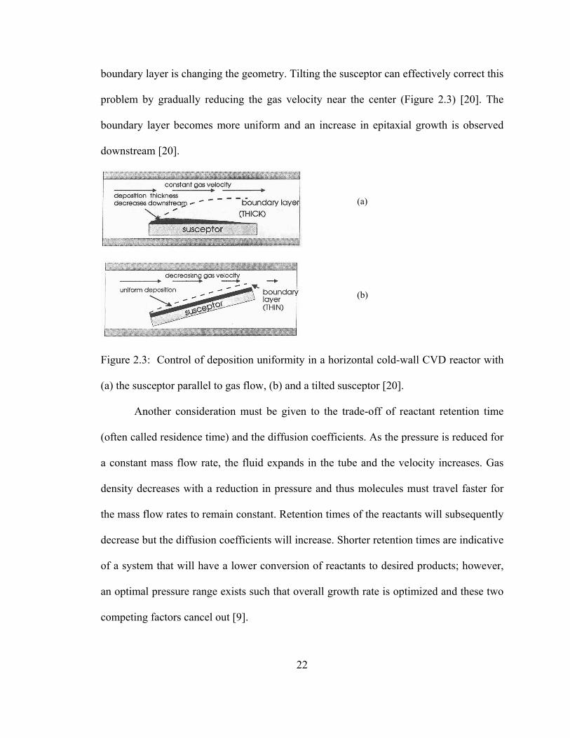
boundary layer is changing the geometry. Tilting the susceptor can effectively correct this
problem by gradually reducing the gas velocity near the center (Figure 2.3) [20]. The
boundary layer becomes more uniform and an increase in epitaxial growth is observed
downstream [20].
Figure 2.3: Control of deposition uniformity in a horizontal cold-wall CVD reactor with
(a) the susceptor parallel to gas flow, (b) and a tilted susceptor [20].
Another consideration must be given to the trade-off of reactant retention time
(often called residence time) and the diffusion coefficients. As the pressure is reduced for
a constant mass flow rate, the fluid expands in the tube and the velocity increases. Gas
density decreases with a reduction in pressure and thus molecules must travel faster for
the mass flow rates to remain constant. Retention times of the reactants will subsequently
decrease but the diffusion coefficients will increase. Shorter retention times are indicative
of a system that will have a lower conversion of reactants to desired products; however,
an optimal pressure range exists such that overall growth rate is optimized and these two
competing factors cancel out [9].
(b)
(a)
23
2.1.3 Surface Kinetics and Equilibrium
The mechanisms by which CVD reactions occur are similar to heterogeneous
catalysis where gaseous reactants adsorb onto a solid surface and then react to form a
new surface. The kinetic rate law for this type of reaction is very complex, due to the
many steps involved, making the ideal design equations difficult to implement [5].
Arriving at a rate law is beyond the scope of this thesis but an understanding of the
concepts that affect the kinetics would be helpful. Transportation of the solute species to
a point near the surface was discussed in the previous section but one should understand
that this is not directly associated with the actual catalyzed heterogeneous surface
reaction but only a necessary function for the reaction steps to occur. When reactive
species approach the surface, adsorption takes place which is characteristic of a
heterogeneous surface reaction. Two types of adsorption that are possible are physical
adsorption and chemisorption.
In physical adsorption, van der Waals forces tend to play the biggest role. Van der
Waals forces are weak but act over a long range where the energy released is on the order
of the enthalpy of condensation [37]. When a molecule interacts with the surface its
energy dissipates as a result of friction and eventually settles onto the surface. This is
analogous to a ball bouncing on a surface and eventually coming to a rest after its kinetic
energy has been spent. The molecule maintains its identity in physical adsorption since
there is not sufficient energy to break bonds [37]. Physical absorption may also take place
in CVD, such as large particle deposition, but is generally considered undesirable in
microelectronics epitaxy and lengths are taken to avoid this absorption mechanism.

24
The type of adsorption that takes place for catalyzed heterogeneous surface
reactions, and the one that is considered to be the dominant part of the rate of the surface
reaction, is chemisorption. In chemisorption, the adsorbed molecule is held onto the
surface by valance forces resulting from surface defects. The electronic structure of the
adsorbed molecule is perturbed, causing it to be reactive [5]. The key to SiC CVD is Si
atom surface mobility since transport of atoms to the surface is required to grow a film.
Off-axis substrates in SiC epitaxy play a critical role in this process due to the irregular
surface it provides. A step may have defects of its own known as kinks. When an atom or
molecule comes into contact with a terrace it bounces across it under the influence of
intermolecular potential and may come to a step or a corner formed by a kink [37] which
effectively lowers the activation energy of the growth process. The activation energy is
the energy required to force the slowest reaction step (adsorption for SiC epitaxy [9]) that
limits growth to proceed. The species has a higher probability of interacting with more
surfaces in step-flow epitaxy and may become adsorbed.
Figure 2.4: Steps and terraces on an off-axis substrate play a large role in surface growth
and catalysis due to kinks and surface defects.
Step
TerraceKink Molecule

25
Once a molecule has been adsorbed onto the surface a number of different
reactions could occur to form the desired product [38]. Taylor [39] suggested that the
reaction is not catalyzed over the entire surface but only at certain active sites resulting
from surface irregularities such as chemisorbed molecules. The surface reaction could be
a single-site mechanism in which only the adsorbed molecule is involved. Alternatively,
the surface reaction may be a dual-site mechanism where the adsorbed molecule interacts
with another site to form the desired product. This second site may be occupied or the
reactant will actually interact with both sites. Lastly, the reaction could take place
between an adsorbed molecule and a molecule in the gas phase. The actual mechanism
for any surface reaction is possibly a combination of the three possibilities although each
one has a different rate law [5].
Figure 2.5: Schematic of reactant adsorption on the growth surface in CVD. Once a
molecule has been adsorbed onto the surface (a) a single site mechanism, (b) a dual site
mechanism, or (c) a single site with a gas phase interaction could occur.
(a)
(b)
(c)

26
The last step for a heterogeneous surface reaction is the desorbtion of the by-
products. This is much the same as the adsorption process except in reverse. The by-
product no longer has valance forces holding it in place and become loosely bound to the
surface by van der Waals forces [37]. These by-products are thus highly volatile and
readily release from the surface and they desorb. The by-products are then transported,
via diffusion through the boundary layer, enter the gas stream and are then swept
downstream to the reactor vent. The adsorption, surface reaction, and desorbtion steps are
all critical steps to epitaxy and the operator can use the knowledge of these phenomena to
understand and improve the growth process.
It has been argued that a low pressure system would effectively increase growth
rates due to the larger diffusion coefficients making it a reaction-rate limited growth
regime. Forethought should also be given to any possible negative effects a reduction of
pressure would have on the kinetics. Partial pressure of the gases are decreased with an
overall reduction in pressure making them factors in the ability of the gas to reach the
surface and react successfully. Although the kinetics of this system described in this
thesis have yet to be worked out, surface reactions in high temperature CVD typically
take place very quickly compared to mass transport making it unlikely that a reduction of
pressure would have a significant effect on the overall reaction rate. Careful weight
should be given to the factors previously mentioned when selecting operating parameters
but it can not be clearly stated what the rate limiting SiC CVD steps are until a careful
kinetics and mass transport study is completed. It has been empirically observed that
growth rates are indeed optimized in a lower pressure SiC CVD system [11], most likely
due to increased mass transport through the boundary layer.

27
An important aspect of step flow epitaxy is that it encourages lateral growth.
Molecules tend to migrate towards surface steps and kinks where catalytic reactions take
place. This means that three-dimensional growths are inhibited since a molecule migrates
across the surface until it hits a defect or step thus epitaxial layers want to grow one step
at a time and thus form a two-dimensional film. If the ideal step height existed, the
epitaxy would take place one monolayer at a time. SiC growth is, however, prone to
defects including screw dislocations, particle nucleation, growth pits, etc., particularly
when growth rates are high [2], leading to three-dimensional growths which are highly
undesirable. Suitable process chemistry can be used to suppress poor morphology
resulting from these defects and it has been demonstrated for sometime that growth on
off-axis substrates suppresses three-dimensional nucleation.
2.2 SiC CVD Epitaxial Growth Chemistry
SiC CVD chemistry is quite complex due to the large number of possible
reactions and side reactions. Fortunately an analysis of growth is greatly aided by general
knowledge even as the specifics are difficult to know for certain. SiC CVD chemistry is
compounded to a great extent by the high temperatures required, the number of possible
precursors, and the carrier gas which have implications with regards to the materials in
the reactor as well as the epitaxy. This discussion will focus on derogatory results, related
to chemistry, which have been observed during the course of SiC CVD development.
Chapter one detailed the use of a Si/C ratio to control doping by using the site-
competition effect [23]. There are, however, additional chemistry issues related to this
ratio which we will now discuss. A low Si/C ratio is desirable not only to achieve low n-
type doping levels, but also for preferable surface morphology. The chemistry of surface

28
morphology can be classified into three types: C rich, Si rich, and moderate (Si and C
flux being comparable). Although there have been many types of precursors used to grow
SiC films, silane (SiH4) and propane (C3H8) are the sources of Si and C used in most
systems and the system at USF. Under moderate conditions a more stoichiometric
deposition is observed where morphological defects are less prone to occur. Si richness is
perhaps the most common problematic case due to the lower decomposition ratio of
C3H8. Cracking patterns reveal the existence of Si and SiH2 due to cracked SiH4 while
carbonaceous species such CH4, C2H2, C2H4, etc. result from cracked C3H8 [40-41]. This
suggests that Si species are preferably absorbed on the reactor surfaces thus encouraging
a Si rich growth surface. Si rich conditions tend to produce three-dimensional particle
nucleation because of the polymerization and subsequent deposition of elemental Si [9].
Si rich growth conditions can be inhibited during the growth cycle by decreasing the Si/C
ratio and by introducing SiH4 only when C3H8 is in equilibrium. C rich growth has been
discussed in relation to graphite decomposition in the susceptor and Si desorbtion in
process heating. Typical C rich morphological defects include graphitization and wavy or
stripe-like morphology.
The effect that a low-pressure system has on chemistry relates to prevention of
gas-phase precipitation. In this effect, a reaction occurs in the gas phase and subsequently
at the substrate growth surface. The unintentional deposition of these relatively large
particles causes nonuniformity in the epitaxial film and poor surface morphology [18]. As
discussed, thermal cracking of silane leads to elemental Si in the system that has the
potential to form Si clusters known as Si droplets. Gas phase nucleation takes place by a
polymerization leading to the formation of particles ranging in size up to approximately

29
300Å [42]. Another negative effect of this phenomenon is that severe depletion of Si in
the vapor phase limits the amount of Si available for a surface reaction. A reduction in
overall pressure would reduce the partial pressure of Si making it less reactive in the gas
phase and shifts the phase equilibrium of the system to prevent vapor condensation [9].
Indeed it was with this anticipated benefit that this thesis research was undertaken.
An excess of C from the susceptor during growth can change the Si/C ratio in the
system significantly. The excess C can cause two problems; graphitization leading to
morphological defects in extreme cases and lack of dopant control via site-competition
due to an excess of uncontrolled C in the gas stream. This problem has been observed in
the USF reactor where freshly exposed graphite, due to SiC-coating cracks on the
susceptor, was obvious visually and resulted in poor morphology during growth runs
where this was observed. Although SiC coated susceptors are capable of producing high-
quality epitaxy, graphite exposure due to wear of the coating is a continuous problem in
these systems and must be carefully monitored.
The lifetime of the susceptors and quality of the epitaxy has been indicated to be
improved by applying a tantalum carbide (TaC) coating on the graphite surface [43] since
this coating is more durable than the conventional SiC coating used during these
preliminary experiments. Poly-crystalline growth on the back-side of the substrate is
observed when the SiC coatings are used as the coating transfers to the substrate during
growth thus making a TaC coating even more desirable for homoepitaxy application
(since TaC is a dissimilar material it does not transfer to the substrate and no poly-
crystalline film is grown on the backside). TaC coatings may not be used when using Si
substrates for 3C-SiC epitaxy because any residual Ta that did not form TaC during the

30
coating process forms a low temperature eutectic with Si at the temperatures required for
3C-SiC growth [8].
The discussion in Section 2.1.3 regarding adsorption and desorbtion has
implications regarding the surface chemistry. The solid-vapor equilibrium that exists is
highly dependent on temperature thus precautions must be taken when ramping the
temperature to growth conditions prior to introducing the precursors [11]. The vapor
pressure of a heated SiC surface has incongruent vapor pressures due to Si and C atoms
existing in equilibrium at the surface (note that the lattice can be thought of as 2
interdependent Si and C sub-lattices, each with their own vapor pressures). Si is the lower
vapor pressure substance which will readily evaporate in the absence of a C etching gas
or a lack of Si overpressure. This incongruent vapor pressure may result in two
disastrous effects: graphitization of the surface or formation of Si droplets leading to
morphological defects during the subsequent growth process. The later is a result of the C
removal rate being higher than Si when a C etching gas is used such as hydrogen. A small
amount of hydrocarbon or a Si etching gas introduced during the heating/etching process
has been shown to adequately prevent morphological problems associated with Si
droplets [44-45].
Figure 2.6: Typical morphological problems resulting from CVD chemistry.
(a) (b)

31
The carrier gas for most SiC CVD systems is hydrogen. Several factors are
involved with this choice including its ability to prevent graphitization during the heating
process. Hydrogen is used as a carrier because a comparatively larger stoichiometric SiC
deposition area is obtained, which is presumably due to the ability of hydrogen to inhibit
the formation of radical species [46]. Additionally, hydrogen is economical and is
available in ultra-high-purity (99.999% pure). There are, however, some drawbacks to
using this gas. Etch rates of the graphite susceptor increases exponentially with
temperature in the presence of pure hydrogen [47].
It has been observed that a hydrogen carrier gas influences the etch rate of SiC
during the growth process and will produce gaseous hydrocarbons and free Si [48]. Since
the reaction that produces a SiC deposition is an equilibrium reaction, the reverse is
possible and is governed by Le Châtelier’s principle[49]. When a chemical system in a
state of equilibrium is disturbed, it retains equilibrium by undergoing a net reaction that
reduces the effect of the disturbance. The presence of pure hydrogen in the hot system
may cause a decomposition reaction of the substrate. This decomposition is the basis for
the etching process that is common in SiC CVD to remove surface material that may be
“damaged” from prior processing steps (such as polishing). Additionally, the equilibrium
present in the system during growth has a net growth rate which is the growth rate minus
the etch rate.

32
Figure 2.7: Illustration of the competing etch and growth mechanisms on an off-axis
“vicinal” 6H-SiC substrate.
The numerous possible gas and surface chemical specious, along with the possible
surface reactions, further emphasize the state of equilibria of the system. In order for a
reaction to take place the reactants must proceed to a lower energy state to form products.
This energy change is known as the free-energy change of the reaction, or ∆Gr°, which
varies as a function of the type of reactants, the molar ratio of the reactants, temperature,
and pressure [18]. One can assess the feasibility of a reaction occurring by solving the
related equations [20] and obtaining a value for ∆Gr°. The reaction is said to favor the
reactants if ∆Gr° is positive, favor the products if ∆Gr° is negative, and be at equilibrium
when it is equal to zero. This assessment is only valid if the reaction contains the major
species that exist at equilibrium. Table 2.1 lists the common species that may exist in the
system which was determined by Lofgren et al [50] by modeling the likely
decomposition and surface reactions.
3.5º
[0001]
[1100] [1120]
Direction of Etching Direction of Growth

33
Table 2.1: Probable specious exhibited during SiC CVD using silane and propane
precursors in a hydrogen carrier gas [50].
Gas Phase Specious Surface and Bulk Specious
C-Containing Si Containing Other Surface Bulk
C Si H C C CH Si2 H2 CH Si CH2 Si3 Si CH3 SiH SiH CH4 SiH2 SiH2 C2H SiH3 HCa C2H2 SiH4 HSib C2H3 Si2H2 C2H4 Si2H3 a H atom adsorbed at a C site C2H5 H2SiSiH2 b H atom adsorbed at a Si site C2H6 H3SiSiH C3H2 Si2H5 H2CCCH Si2H6 C3H4 Si3H8 CH2CHCH2 C3H6 i-C3H7 n-C3H7 C3H8
As previously discussed, the carrier gas is initially saturated with precursors and
becomes less saturated as reactants are consumed thus depleting the driving force for
transport along the length of the reaction area. The result of this is often seen as dopant
nonuniformity as the impurities can out compete the Si and C atoms when they are
depleted [23]. Work done by Koshka et al [51], using CFD simulations coupled with
experimental validation, confirms a depletion of reactants along the length of the
susceptor in a horizontal cold-wall CVD reactor indicating a mass transport limited
regime. An analysis of the experiments shows growth rate uniformity, surface

34
morphology, and doping uniformity where highly dependent on placement of the sample
with respect to the susceptor area [51] due to altered chemistry at different positions. The
practical consideration which comes out of this study is the need for consistent substrate
placement on the susceptor. The operator must place substrates consistently in order to
perform repeatable growth studies.
As the precursors enter the heated area, decomposition and consumption occurs
resulting in a distribution that is further effected by fluid dynamics. The mole fractions of
the possible species along the susceptor length are useful in refining growth processes
and susceptor design. Since the mole fractions are indicative of the growth rate and
uniformity of the system, this type of modeling represents some of the latest advances in
CVD chemistry.
Figure 2.8: Temperature and gas mole fraction just above a susceptor surface as
determined by Lofgren et al [50] for a hot-wall SiC LPCVD reactor.

35
2.3 Summary
CVD operation and design involves an understanding of fluid dynamics, kinetics,
and transport phenomena. The complexities of these concepts make CVD growth a
challenging area which can be analyzed with experimental and analytical tools. Process
refinements can be performed on a regular basis using empirical observation coupled
with experimental validation. More complicated areas, such as fluid dynamics, are better
approached through CFD simulations to design the geometry of the reactor.

36
CHAPTER 3
CVD SYSTEM DEVELOPMENT
3.1 APCVD SiC System
It has been stated that the manipulation of process parameters and reactor
geometry can be used to control the growth of epitaxial layers of SiC. The essential
components needed to construct a CVD reactor can be selected and/or designed and
constructed with planning and careful attention to engineering principles. The system
must be designed to be fail-safe with equipment that can handle the extreme environment
of SiC processing, especially the high growth temperatures (>1600°C) and highly
reactive gases such as silane and hydrogen. The primary components that one must
consider are the same for all CVD reactors, namely the gas handling system, reaction
vessel, susceptor, RF delivery and coil design (for inductively heated systems), automatic
process control, and an exhaust package.
The AP design was largely the result of previous work conducted on a nearly
identical system by members of our group [30]. Distinctions exist between the previous
design and the USF system but the basic components of a horizontal reactor capable of
epitaxy on up to a 2 inch substrate still is the same. The main ideas carried over from the
other reactor are the control system design and essential instrumentation required to
monitor the process. A programmable logic controller (PLC) and microprocessor were
designed and constructed to allow fail-safe safe operation of gases, purging of the vessel,
gas metering, and temperature control.

37
Figure 3.1: Block flow diagram of the APCVD System at USF [30] which preceded the
LPCVD design to be discussed in Section 3.2.
3.1.1 APCVD Tube Design
The APCVD tube design was performed by Burke, Schattner, and Saddow [29-30] at
Mississippi State University for a CVD system similar to the one at USF. The essential
element that must preface any CVD reaction tube design is the basic diameter it must be
to accommodate the substrate on which the epitaxial layer is to be grown. 75mm SiC
wafers are now commercially available, although growth on 50mm substrates is still the
commercial standard at this time. Typically the susceptor is designed slightly larger than
the substrate to ensure maximum temperature uniformity hence a 70mm wide susceptor,
to permit growth on a 50mm substrate, was used as the basis for specifying the tube inner
diameter (ID). Assuming the susceptor can be evenly heated and reactants can be
uniformly delivered to it, a tube ID slightly larger than the susceptor can be selected as a
first iteration step to sizing the reaction vessel. The diameter must be large enough so that
Microprocessor Control Unit
Programmable Logic Controller
Pyrometer
Gas Supply and Delivery
Control Console Reactor Cabinet
Cooling Water
Exhaust to Burn Box and Scrubber
Reaction Tube
RF Generator

38
the susceptor will have adequate spacing from the quartz tube wall. The overall length of
the tube can be roughly estimated based upon practical heat transfer considerations and
development of fluid flow regimes. This process of sizing the tube and selecting the
geometry often takes multiple attempts to optimize all parameters resulting in an iterative
process [29]. The iterations generally consists of choosing a carrier gas flow rate, analysis
of dimensionless number (Reynolds, Grashof, and Rayliegh), and finally a computer
simulation to confirm laminar flow in the susceptor area.
The final design selected for the USF APCVD reaction tube consists of a head tube
section, a water-cooled reaction tube, a quartz boat that supports the susceptor, and an
end cap. A 100 mm bore diameter was used with an overall length of 30 inches. The head
tube section permanently clamps onto the reactor housing and provides the quartz to
metal transition. The successive sections clamp onto the head tube sections using bake-o-
lite clamps with Viton o-rings for vacuum integrity. This design has been shown to
hold adequate vacuum for CVD (< 50 mTorr) but other designs, such as differentially
pumped double o-rings, are desirable to ensure maximum vacuum integrity. The main
body of the reaction tube is water cooled to reduce heat accumulation in the system and
provide cooling for the o-ring joints, which have a maximum operating temperature of
~150°C. The end cap then provides the transition from the reaction tube to the gas
exhaust system.
3.1.2 Susceptor Development
The methods of designing a susceptor with sufficient RF coupling range from
complex simulations to empirical observation coupled with practical considerations. The

39
desired result is a substrate that is heated uniformly. The basic idea of RF inductive
heating of a graphite susceptor is to use a RF generated magnetic field to couple onto the
graphite, which consequently produces eddy currents in the graphite which heats the
graphite through Ohmic (i.e., I2R) heating.
The convective cooling effects of the process gases and radiation from the
susceptor represent challenges in creating a susceptor that will heat uniformly and at the
desired temperature. Convective cooling occurs primarily at the topside of the susceptor
while radiation losses occur most intensely at the edges of the susceptor. Cooling can be
significantly greater at the front of the susceptor due to the cold finger of the inlet gases
extending into the hot region. With a practical assessment of these facts, one can
conclude that the majority of the RF power should distribute to the areas with the greatest
load (i.e. – the edges, top side, and front side).
Figure 3.2: Schematic representation of graphite susceptor under active heating and
cooling. Convective cooling occurs primarily at the topside of the susceptor while
radiation losses occur most intensely at the edges of the susceptor.
Process gas flow
Convective Cooling
Intense Radiation loss

40
These cooling effects can be overcome by shaping the susceptor’s geometry to
minimize their effects and by proper spacing of the RF coils. Increasing the amount of
graphite material in the areas of most intense cooling is a good approach to dealing with
these issues. More graphite mass translates into more RF coupling at those areas (in
addition to thermal mass) and thus the delivery of more power. In addition increasing the
thermal mass in these regions reduces the temperature dips associated with convective
cooling. It follows from Figure 3.2 that having more graphite material at the edges and
topside would deliver more coupling to the appropriate areas. This can be accomplished
by having the susceptor machined such that material is removed on the bottom side as
shown in Figure 3.3.
(a) (b)
Figure 3.3: Material is machined out of the underside of the susceptor (a) to deliver less
power to the areas that are subject to less cooling load and increase the thermal mass at
the edges and topside (b) where the cooling load is at a maximum.
To counteract the effects of the cold gas finger extending into the front area of the
susceptor, the RF coil design comes into play. A complete design of the coil is beyond

41
the scope of this thesis but a short discussion is necessary to understand the effects that
coil spacing has on power delivery. An ideal coil would have the turns placed as close
together as possible without touching. This is because the coil is basically a solenoid and
the magnetic flux from each coil adds to yield the resultant inductive field at the
susceptor. Thus any spacing in the coil represents power losses due to fringing flux lines
and this fact can be used to deliver more power to the front of the susceptor, where the
power is needed. Gradually increasing the coil spacing from front to back can increase
the temperature uniformity and counteract the cold gas finger effect. Properly designing a
coil in this manner will intentionally introduce power losses where needed and can
drastically improve uniformity. The turning and testing of several coils resulted in an
optimal design with the coil spacing as close as possible at the front of the growth zone
and slightly increasing spacing near the end. Professionally turned coils could further
optimize heat delivery and provide better specifications and should be considered in the
future if susceptor performance is found to be inadequate.
A standard method of testing temperature uniformity and calibrating heating
instrumentation in SiC CVD is the so-called Si melt test. Since the melting temperature
of Si is close to the growth temperature, one can use this to accurately define the
temperature uniformity of the susceptor near growth conditions. In this test, small pieces
of Si are placed on the graphite susceptor and then heated until melting of the Si pieces
(at 1410°C) are observed. Alternatively, the Si pieces could be placed on a SiC substrate
(on top of the susceptor) as to not damage the susceptor. An IR pyrometer is aimed at the
back edge of susceptor so one must determine the temperature error between the
measurement point (susceptor back edge) to the top side where growth takes place.

42
Basically, when the Si is observed to melt the surface temperature is exactly 1410°C. The
pyrometer temperature reading is then recorded and the difference (∆T) is noted.
Additionally, the temperature across the growth surface must be as uniform as possible so
several pieces of Si should be placed to measure and verify the uniformity. This
calibration is the most accurate developed but may produce some inaccuracy since
process temperature can be much higher or lower and ∆T is not constant except at
1410°C. However, this is a good starting point for CVD processing and is the accepted
standard for most SiC CVD growers.
Several melt tests were performed at USF for various susceptor arrangements and
specifications. The best design was observed to have a temperature gradient of less than
15°C along the reaction area, which is reasonable when compared to other research grade
CVD reactors that utilize similar power delivery systems[52]. The dimensions for this
design were 80mm x 70mm x 20mm with a groove of 60mm x 50mm x 5mm removed
from the bottom. All corners had a 5mm radius to prevent hot-spots (radiation losses) at
the corners.
3.1.3 Processing Hazardous Gases
Gas handling, exhaust, and tube sealing management are critical in CVD due to
the hazardous nature of the process gases. The hazardous process gases involved, namely
SiH4, make design and testing paramount to safe operation. Proper design must ensure
purging of all gas lines during start-up and shut-down to safely handle these process
gases. All seals and materials were selected to ensure maximum integrity and be versatile
enough for research grade use.

43
The manifold for gas distribution is capable of handing Ar, H2, C3H8 (97% H2),
SiH4 (97% H2), 3% N2 (97% H2), and an auxiliary gas for future work. The manifold
provides 3 basic functions: process gas to the reaction tube, purge gas to the reaction
tube, and process gas to the vent. The PLC and PC control these functions [30] by
outputting user input and ensuring fail-safe operation. The 2 basic modes of operation are
“process monitor” and “purge” mode. Venting of gases can be done in any mode but the
other functions are restricted. Process gases can only be active when the control system is
in “process mode” to avoid dumping flowing gas when the system is not properly
configured. The process and vent function meters, via mass flow controllers (MFC’s)
under PC control, the supply gas and directs it to the appropriate line via an isolation
valve that allows flow to either the vent or process manifold (or both). The isolation
valves are controlled by the user via the control system front panel which sends a signal
to the corresponding solenoid based on user input and internal safe operation checks. Gas
flow to the process manifold is also controlled by the PLC to ensure the reactor is in the
correct configuration, as stated above. The purging function can deliver Ar or H2 from the
gas manifold via a small section of stainless-steel line preceding the tube and
subsequently through the tube and exhaust system. Purging of Ar occurs automatically
when any interlock is compromised. The manifold was constructed of stainless steel
using VCR connections so that the system was modular (for maintenance and
modification purposes). Figure 3.4 is a diagram of the gas handling system, including the
manifold and should provide the reader with a more complete understanding of the
system.

44
The seals of all process lines should be selected and tested as rigorously as
possible. Even the tightest seals are subject to small leak rates due to pressure gradients.
A standard vacuum check should be performed whenever a seal is compromised such as
tube changing and routine maintenance. Alternatively, some lines are more appropriately
checked by holding high pressure for a prolonged time period (12-24 hours). The most
effective test used during the development was helium leak detection. This tool uses mass
spectroscopy, tuned for He, to analyze the molecular flow inside the vacuumed lines
being tested. The seals can be saturated with He by applying a small amount (~1 ml/min)
around the perimeter of the seal which, if a leak exists at that point, is then drawn into the
vacuum system and subsequently into the analyzer. Using this technique, a 10-8 Torr
partial pressure He leak was found. The only drawback to this test is that the vacuum
conditions required (<50 mTorr) do not necessarily represent the processing conditions.
Essentially this means that leak rates can radically change over different pressure
gradients and may not be found with the detector. However, since 50mTorr is below the
LPCVD process pressure, this represents a “worst case” scenario and likely is the best
means for securing many leaks in the system. A combination of the various methods can
be applied to ensure the integrity of the gas handling system.

45
Figure 3.4: Diagram of the gas handling system. The manifold is outlined by the dotted
line as shown.
SiH4 is pyroflouric even in dilute concentrations thus an explosive risk is
possible during all phases of processing with SiH4. Additionally, SiH4 tends to produce
SiOx particulates even with small amounts of O2 present, which may accumulate without
proper design and maintenance procedures. This residue can be from SiH4 reactivity with
oxygen that out-gasses from the quartz reaction tube or from small leaks in the process
lines. SiOx is an explosive risk in itself and must be eliminated whenever possible. For
these reasons, purging is absolute necessity in all lines that contact SiH4 before and after
use. A purge panel was salvaged and modified for the purpose of purging the main gas

46
line that goes from the SiH4 bottle to the isolation valve at the manifold. A standard Ar
purge is used to completely purge down the lines after use.
3.2 LPCVD SiC System
The design of the low-pressure system was implemented from June 2002 to
May 2003 by the author. The need to stay with the current trends in CVD as discussed in
Chapters 1 and 2 led to a horizontal low pressure reactor design. There are several
elements to this design such as tube modification, plumbing design, pressure control,
pump selection, and operation. Operation parameters are subject to frequent change as
new processes develop so the system was designed with maximum flexibility.
Figure 3.5: Block diagram of the LPCVD system developed during this thesis work.
The new components are the low-pressure exhausting system shown on right.
Microprocessor Control Unit
Programmable Logic Controller
Temperature Sensor
Gas Supply and Delivery
Control Console Reactor Cabinet
Pumping Package
Throttle Valve
Pressure Controller
Cooling Water
Pressure Transducer
Particulate Trap
Pump Exhaust to Burn Box and Scrubber
Dry Pump
Reaction Tube
Pressure Sensor
RF Generator

47
3.2.1 Basic Design Considerations
The design of a low-pressure pumping system may be arrived at by attention to
classic fluid flow design rules. Resistance of the fluid flowing against the pipe walls and
fittings is important in viscous flow regimes which are the operation parameters in this
version of LPCVD. Molecular flow is typically recognized to occur when pressures are
less than 50 mTorr, which is not the case for the USF LPCVD reactor except during
vessel purging. SiC LPCVD is conducted around 100 Torr. Therefore viscous fluid flow
design equations dominate most considerations here. However, the system is subject to
the molecular flow regime during initial pump downs to evacuate the vessel but this is
not a condition that occurs during LPCVD growth. The vacuum design must take into
consideration this most important function by estimating system pump down so that
proper pump selection can be made.
During a pumpdown from atmospheric conditions, the system passes through
different types of flow regimes. As pumpdown proceeds, flow begins as very turbulent
and transitions to laminar flow as the average velocity of molecules leaving the system
decreases. These types of regimes are viscous, with molecules dragging each other from a
short mean free path. As the pressure is reduced further, the mean free path lengthens and
the molecule collisions decrease brings the flow regime into molecular flow. The term
molecular flow is used to describe molecules transferring back and forth in a random
motion. The continuous force applied by the pump causes a pressure gradient and thus a
density gradient. This density gradient changes the volumetric flow throughout the
process lines but the mass flow rate will stay the same during steady state.

48
The mass flow rate is called the throughput (Q) and is a measure of the number
of molecules passing a given plane per unit time. The units Torr-liters per second
conventionally represent mass flow rate in vacuum systems which comes from the ideal
gas law (pressure times volume is a measure of a quantity of gas). Considering a general
system where gas is leaked in and subsequently pumped out one can see that the pressure
is different at different parts of the system. At steady state the pressure decreases from the
gas inlet to the reactor to the pump which is obviously the low pressure point of the
system. In this case the throughput is the same throughout the vacuum system since there
is no accumulation of the molecules along the vacuum path.
The volumetric flow rate at any point in the system is called the pumping speed
(S). The units of pumping speed are thus liters per second. The throughput is the same
throughout the system but the pumping speed is not since the gas is continuously
expanding as it flows towards the pump. The volumetric flow rate then increases as the
fluid moves closer to the pump. The pumping speed and throughput are related by Q =
SxP.
Selecting vacuum component and sizing lines involves analyzing fluid
resistance or the inverse (conductance) and can be determined by vacuum sizing
equations [53]. The pipe walls and various geometries the fluid may have to travel
through causes friction and thus resistance. With the obvious electrical analogy, the
resistance Z is defined as the proportionality constant between pressure drop and mass
flow and the inverse is the conductance C.
21 PPQC−
= [1]

49
In viscous flow regimes conductance can be further defined as
LPDCv
43000= , [2]
where P is the average pressure, in Torr, D is the tube diameter, in inches, and L is the
length, in inches. Assuming the fluid is dry air at 20°C the constant 3000 applies giving C
the units of liters per second. All of this is, of course, assuming the ideal gas law and
using Bernoulli’s equation to relate pressure difference.
The conductance and pumping speed have the same units but they are not
synonymous. Conductance is a property that expresses the amount of three dimensional
spaces while pumping speed is a property of position. The conductance of a fitting
describes the resistance to the fluid from the volumetric and surface area while a pumping
speed describes the mass flow rate for a given pressure. Calculating conductance is
essential to designing a vacuum system as a larger conductance is more desirable for
higher vacuum conditions. To arrive at a large conductance, large diameters and minimal
lengths should be incorporated. More collisions with the walls occur for more wall
surface area. In molecular flow, more collisions give the opportunity for a molecule to go
the wrong way; hence pumpdowns occur much more rapidly for higher conductance
systems.
The volumetric flow rate through the inlet of the pump is referred to as the
pumping speed of the pump, Sp. If a passage from the vacuum chamber to the pump is
known to be Ct, then the volumetric flow rate at the chamber, S1, is of interest for CVD.
Using S1 to be the desirable volumetric flow rate based on CFD simulations, one can size
and select lines and fitting to obtain Sp that is reasonable to select a pump.

50
Figure 3.6: Main parameters in sizing a vacuum system. S1 is the volumetric flow rate
exiting the chamber and Sp is the pumping speed at the pump. Ct is the total conductance
estimated through the lines and fittings that connect the chamber and the pump.
In SiC CVD deposition of SiOx is a reality that must be considered in all
components. A pleated paper particulate trap capable of capturing particles greater than 2
µm was evaluated to be the best option to remove as much SiOx as possible. The only
other option may be to heat the lines to reduce particulate accumulation. This filter was
placed about 20 inches downstream of the reaction tube to promote particulate trapping
upstream immediately from sensitive downstream instruments such as the pressure
transducer and throttle valve. Equilibrium will shift as the flowing fluid cools and SiOx
contamination is always a risk so one must select robust components that will tolerate
harsh service.
3.2.2 Computational Fluid Dynamics Simulations
The CFD simulations were performed by Timothy Fawcett of the USF SiC
group and were presented at the 2002 AIChE annual conference [54], which described
some of this thesis work. The theoretical discussion in section 2.1.1. was applied to this
project via simulations using FIDAP 6.0 [55]. The mesh used to solve for the input and
Chamber Pump
Ct
S1 Sp

51
output of finite cells is displayed in Figure 3.7. A fine grid was used in the reaction area
to maximize the accuracy of the analytical results shown in Figures 3.8-3.11. A
Temperature profile for the APCVD and LPCVD cold-wall systems indicates that the gas
is heated to desirable reaction temperatures only directly near the susceptor. An 8 slm
APCVD gas velocity profile with newly designed endcap for LPCVD is given in Figure
3.9 where laminar flow is evident in the reaction area. 30 slm and 100 mBar LPCVD
velocity profiles predicted an unstable region in the reactor in addition to the non-laminar
flow across the susceptor which indicates undesirable operating conditions as shown in
Figure 3.10. 10 slm and 100 mBar LPCVD velocity profile (see Figure 3.11) display
some back mixing, however, laminar flow in the reaction area makes these process
conditions feasible as a starting point to develop a process.
Figure 3.7: Mesh for CFD calculations as performed by Timothy Fawcett [54].
Dimensions are as follows: Tube bore – 100mm, tube length – 640 mm, gas inlet – ¼”,
gas outlet 40mm. Simulations performed using FIDAP 6.0.
Gas Inlet
Boat Susceptor
Cold Wall
Outlet

52
Figure 3.8: Temperature profile CFD simulation for APCVD and LPCVD cold-wall
system as performed by Tim Fawcett [54].
Figure 3.9: Eight slm APCVD Velocity profile CFD simulation for system with new
endcap as performed by Tim Fawcett [54]. Laminar flow is evident in the reaction area.
• P = 1 atm • Q = 8 SLM • Wall Temp = 60°C • Inlet Temp = 25°C • Susceptor Temp = 1600°C • Re = 365

53
Figure 3.10: Thirty slm and 100 mBar LPCVD velocity profile CFD simulation as
performed by Tim Fawcett [54]. An unstable region, in addition to the non-laminar flow
across the susceptor, indicates undesirable operation conditions.
Figure 3.11: Ten slm and 100 mBar LPCVD velocity profile CFD simulation as
performed by Tim Fawcett [54]. Although some back mixing is evident, laminar flow in
the reaction area make these process conditions feasible as a starting point.
• P = 100 mbar • Q = 10 SLM • Wall Temp = 60°C • Inlet Temp = 25°C • Susceptor Temp =
1600°C • Re = 15
A little bit of back mixing
• P = 100 mbar • Q = 30 SLM • Wall Temp = 60°C • Inlet Temp = 25°C • Susceptor Temp = 1600°C • Re = 46

54
3.2.3 Pressure Control
The first step in design is recognizing the instrumentation that must be
employed to provide desired functions. The target for this system is vessel evacuation
followed by pressure control in the 75-225 Torr range. Vessel evacuation was designed in
the APCVD system so that was kept functional by including a vent bypass to permit
APCVD operation after upgrade to LPCVD. However, pump selection has to address this
issue by providing a low ultimate vacuum for the reactor pump and purge processing
step. The control loop consists of a pressure transducer, control valve, and a pressure
controller which has been left out of the data acquisition loop for simplicity sake although
this option is left open for future work.
By far the easiest and cheapest way to accomplish pressure control is
purchasing a commercially available pressure controller. BOC Edwards model Barocel
600® was selected to provide maximum versatility in the range of 0-1000 Torr. This
model is corrosive resistant all stainless steel construction with a calibrated pressure
measurement when exhaust system temperature is between 15-80 °C. Cooling the piping
with various muffin fans was used to prevent the transducer element from accumulating
heat is excess of this temperature specification. The corresponding controller, BOC
Edwards Downstream Pressure Controller Model 1800®, is capable of proportional
control of valve position based on comparison of user input and the signal from the
transducer. The controller also will lock a desired valve position, provide a “soft start”,
and default to the last valve position if interrupted. The control valve selected, BOC
Edwards Butterfly Valve Model 1850®, is capable of controlling 15-37 slm which gives
versatility over the wide range of future process parameters.

55
Figure 3.12: The pressure control loop. Actual model numbers selected as shown.
3.2.4 Line Selection
The detailed calculation performed during this thesis are listed is Appendix A.
In this section the design procedure used to select the vacuum system components is
discussed and the reader is referred to the appendix for details. Line selection begins with
basic space considerations as well as selection of fittings and instrumentation required.
The reactor at USF had an area below the cabinet specifically to house vacuum
components thus line lengths were basically fixed within this volume. This leaves the line
diameter and the pumping speed as the only real variables to play with in the design
equations presented. The goal of weighing these variables is to minimize the pumping
speed while still have a practical line diameter to install. High conductance, with a small
line diameter compared to the line length (~8ft), results from the viscous fluid flow being
Pressure Transducer
(BOC Edwards
600)
Control Valve (BOC
Edwards 1850)
Pressure Controller
(BOC Edwards
1800)
Controller generates a
signal that is proportional to the error found by the pressure
sensor
The control valve makes an adjustment in conductance
Pressure signal is sent to
controller where it is compared
to setpoint
User Input

56
more significantly influenced by friction with flowing molecules than the walls.
Appropriate engineering for this situation would be to oversize slightly for any
unforeseen increased demand and 40mm hardware is well above a minimal conductance
range as per the calculations in Appendix A. NW40 hardware specifies 40mm diameter
so it was selected. Furthermore, valve selection for process requirements (15-37slm)
would permit NW40 connection to be used. The pump selection can then be made based
on the pumping speed calculated in Appendix A and considerations to the gases to be
processed.
3.2.5 Pump Selection
In the pressure ranges required for SiC LPCVD (75-225 Torr), there are two
types of pumps that may be used; Oil-sealed mechanical pumps, or the more state-of-the-
art dry pumps. Pumping of hot corrosive gases such as SiH4 can lead to precipitation of
hazardous SiOx on the contacted parts. Oil-sealed mechanical pumps have been
developed with purging capabilities as well as Fomblin® Oil (only needed if O2 is
present in system at high concentration or corrosive fluid) and filtration units to deal
with accumulation of SiOx. Dry pumps can more effectively deal with SiOx by
maintaining a high internal temperature and using interstage purging. Costs for each
pump can be carefully evaluated with attention not only to initial cost but maintenance
cost that will be incurred during its life. The initial cost for mechanical pumps is usually
lower than dry pumps for the same capacity but oil and maintenance costs over the
pump’s life can quickly accumulate.
The initial plan was to purchase a mechanical pump with minimal required
capacity to bring the process up, which was 76 l/m (2.6 CFM) per Appendix A. The RV8

57
BOC Edwards Mechanical Pump had adequate pumping speed specifications according
to the pump curve presented in Figure 3.13. Eventually, a QDP40 BOC Edwards Dry
Pump was available during the course of this project and was installed to very adequately
service this process. A pump curve for the QDP40 is presented in Figure 3.14.
As with any research project, numerous challenges were encountered which
forced changes to the initial design made. Initial sizing of the pump indicated that the
RV8 would be sufficient for initial processing and a larger capacity pump would be
purchased if needed to scale up the process. The flaw in this was the high operating
pressure (~100 Torr) caused viscous flow through the pump oil and the process gases
absorbed the oil subsequently draining the pump. While systems do exist to deal with this
problem, pump maintenance and oil costs quickly add to near the cost of a high capacity
dry pump so a dry pump was procured (BOC Edwards QDP40) and operation found to be
satisfactory for the LPCVD operation.
3.13: Pump performance curve for the BOC Edwards model RV8 oil-sealed mechanical
pump [56]. Note that P = 100Torr operation permits ~ 5CFM pumping speed which is
adequate for this LPCVD operation.

58
Figure 3.14: Pump performance curve for the BOC Edwards model QDP40 dry pump
[56]. Note P = 133 mBar = 100 Torr should result in ~20 CFM pumping capacity.
3.2.6 System Installation
The system installation was carried out from December 2002 to May 2003.
Exhaust and pressure control hardware were mounted under the reactor cabinet as the
APCVD design allowed for. NW40 flanges and fittings where used wherever possible to
permit ease of installation and maintenance. The pleated paper filter element has NW25
flanges but extremely high conductance at low vacuum as specified by the manufacturer
make the cost savings over the larger size worthy.

59
Figure 3.15: Diagram of the LPCVD plumbing exhaust system designed during the
course of this thesis. The rough and the vent1 lines are bypasses to allow AP operation
and pumpdowns as provided by AP design [30].
3.3 Hot-Wall
One of the planned system upgrades was to develop a hot-wall epi process
based on the work of Olle Kordina [43]. Dr. Kordina’s academic work [9] contributed
significantly toward the design of our eventual hot-wall hardware. The basic concept has
been discussed in Chapter 2 and components for the hot-wall system were procured near
the end of this thesis work. A hot-wall insert was designed using graphite foam as an
insulator and to suspend the susceptor element. Isothermal design of the susceptor
Pressure Controller
To Vent
PP
Filter
P
Reactor Exhaust
AP Vent Valve
AP Rough Valve
VAC/Vent Valve
N2 Purge
110V
Inlet Shaft Seal
Pump
208V
Thermister Interlocks
Motor Starter
On/Off PWR

60
assembly with minimal RF delivery is critical to this technique. A first iteration design
was made with the help of Dr. Kordina and simulations by T. Fawcett (see Figures 3.14
and 3.15).
RF delivery has to be considered to minimize coupling to the graphite foam and
maximize coupling to the susceptor in order to achieve isothermal heating of the reaction
area at high temperatures (up to 2000°C). A rectangular configuration for the reaction
area was not only detrimental to be optimum for fluid dynamics per Figures 3.16 and
3.17, but also for the susceptor design as well. A susceptor was procured to achieve an
isothermal design. The outside corners have a significant chamfer on them to reduce the
mass being heated and hotspots occurring close to the reaction tube walls. The two piece
design makes machining easier and has been indicated to increase coupling [9]. Testing
and further development of hot-wall is left for future work by Shailaja Rao and S.E.
Saddow of the USF SiC group.
Figure 3.16: 10 slm and 150 Torr hot-wall LPCVD velocity profile CFD simulation
performed by Tim Fawcett [54]. Laminar flow is predicted in the reaction area although
slight turbulence near the head of tube is also apparent.

61
Figure 3.17: 20slm and 150 Torr hot-wall LPCVD velocity profile CFD simulation as
performed by Tim Fawcett [54]. Laminar flow is still predicted in the reaction area with
more severe turbulence near the head of tube.
3.4 Summary
The system design and installation was a compilation of work performed at MSU
and USF. Extensive teamwork was used during the course of this project to utilize all
skills available to the team. The product of this work is a totally integrated control system
with extensive vacuum hardware and process transport. Analytical techniques were used
wherever feasible along with experienced input to develop a system capable of
performing SiC LPCVD. Experimental LPCVD growth trials are the next step in
evaluating this reactor design. APCVD runs were conducted while this reactor was being
further developed to have LP capabilities. Those results will be presented in Chapter 4
and LPCVD future work will be suggested in Chapter 4.

62
Figure 3.18: Researchers monitoring the USF CVD reactor during growth.

63
CHAPTER 4
RESULTS AND CONCLUSIONS
4.1 Experimental Results
The focus of this thesis was the design and development of a reactor capable of
SiC epitaxy thus some experimental validation should be reported. The initial
experiments performed in APCVD will be reported on and should serve as validation for
the overall system design. The discussion in Chapter 2 indicates that LPCVD validation
can be achieved through varying pressure, temperature, precursor and carrier gas flow
rates. Modifications of the reactor vessel and susceptor may also be necessary to achieve
fluid dynamics and/or a temperature profile conducive to uniform growth. Although these
items are directly linked to this thesis it is in the spirit of the team to pass this torch to
other students.
4.1.1 APCVD Homoepitaxy
Growth studies performed early during the course of development of this
reactor will be reported on in this section. Namely growth run numbers: USF-02-010,
USF-02-011, USF-02-012, USF-02-014, USF-02-015, USF-02-016, and USF-02-017.
Gas flow rates were determined based on past experience with this reactor design [17].
The growth temperature was set to 1600ºC and this was calibrated using a Si melt test
and by setting the backside susceptor temperature to 1390ºC. The carrier gas, 100% H2,
flow rate in these runs was 8 slm. 3% SiH4 (balance H2) was always 80 sccm which was
determined previously to have the appropriate saturation [17]. The flow rate of 3% C3H8

64
(balance H2) was varied in accordance with the site competition doping method explained
in Chapter 1 [23]. The Si/C ratio in the aforementioned runs was 0.13, 0.237, 0.11, 0.15,
0.18, 0.15 and 0.18, respectively. USF-02-016 and USF-02-017 were intentionally doped
with 20 sccm 1% N2 (balance H2) to confirm site competition doping was taking place
within the epitaxial layer. Growth time was 90 minutes in all cases. The samples were
taken from the same wafer which was 6H, n-type, off-axis, production grade from Cree.
The growth took place on the polished Si face. The samples were cut from this wafer
using a wafer saw into approximately 1cm x 1cm pieces.
The sample prep consisted of a 15 minute ultrasonic clean in Acetone,
immediately followed by a 15 minute ultrasonic clean in Isopropanol. A deionized water
rinse was carried out after the solvent cleans and followed by a 10 minute hot bath
(~75ºC) in sulfuric acid. Finally, a buffered oxide etch was performed prior to growth for
2-4 minutes. Rinsing with DI water took place before and after the oxide etch and the
sample was finally dried with a N2 so as not to leave water residue.
Two SiC-coated susceptors were used during the course of these runs that
measured 70mm x 80 x 20mm. They were tested to have approximately 5ºC variation
about the sample area. Each susceptor was conditioned for 90 minutes with a Si/C ratio of
0.15 to help ensure equilibria of the depositions during the runs.
4.1.2 APCVD Characterization
Three specific techniques were used to confirm that epitaxy took place. The first
method was optical inspection with a microscope at various magnifications. Image
capture was not available at the time of these experiments thus no data can be presented
here but the surface appeared specular which is typical of uniform epitaxy. Secondly, the

65
samples were cleaved and the cross-sections were analyzed in a scanning electron
microscope (SEM). Due to the inherent difficulty in cleaving SiC, only one sample
displayed an epitaxial layer that was clearly visible (USF-02-010) and is shown in Figure
4.1. Lastly, CV and IV measurements were taken to determine doping profiles and results
are shown in Figures 4.2-4.3.
Figure 4.1: Cross-section SEM micrograph of a post-growth cleaved sample, USF-02-
010. The epitaxial layer is cleary visible to be ~3 µm indicating a growth rate of ~2 µm/hr
for this 90 minute growth run.

66
Doping Density for various Si/C Mass Ratios
1E+15
1E+16
1E+17
1E+18
0 0.2 0.4 0.6 0.8 1
Depth (um)
Den
sity
(cm
^-3)
0.18 (doped) USF-02-017
0.18USF-02-015
0.24 USF-02-011
0.15USF-02-014
0.15 (doped) USF-02-016
0.11USF-02-010
0.13USF-02-010
Figure 4.2: Doping profiles determined by CV/IV measurements for the APCVD runs
performed during this thesis work to validate the process. The Si/C for each run is
indicated.
Doping Density vs Si/C Mass Ratio
1E+15
1E+16
1E+17
1E+18
1E+19
0 0.1 0.2 0.3 0.4 0.5 0.6 0.7
Si/C Mass Ratio
Dop
ing
Den
sity
(cm
^-3
unintentionally doped
intentionally doped
Figure 4.3: Linear regression analysis of average doping densities for various Si/C ratios.
This proves that the APCVD process developed during this thesis was consistent with the
site competition model.

67
4.2 LPCVD System Validation
System validation was made by performing heat and pressure control tests at
desirable carrier gas flow rates. Desirable flow rates can be defined as 15-37slm in the
pressure range of 75-225 Torr at growth temperature (~1600ºC). The system was
designed with these parameters, as discussed in Chapters 2 and 3, to provide maximum
versatility over the lifetime of the reactor. Modifications to this system would likely be
necessary to provide functionality outside of these parameters. The first LPCVD growth
run, which proved the system performance to be within the design specifications, was
conducted under the following process conditions: Run No. USF-03-072, P = 35 Torr, T
= 1580ºC, H2 = 10 slm, 3% SiH4 = 80 sccm, and 3% C3H8 = 80 sccm (Si/C = 0.30). The
result was a very nice single crystal epi layer also observed under the optical microscope.
Further growth studies are required to fully validate the system [8].
4.3 Summary
LPCVD system design and development was intended to produce repeatable
SiC epitaxy with doping control on substrates ranging in size of up to 2 inches while
having fail-safe operation and adequate process control. Growths rates are important
factors as well which should produce uniformity of epitaxial layers and doping densities.
A system capable of achieving such standards was developed for APCVD operation and
further developed for LPCVD. The LPCVD addition was designed and implemented with
the intention of refining epitaxy uniformity and increase growth rates.
The APCVD system was a reproduction of other systems designed by Dr.
Saddow [30] and required intensive work by this author, along with a supporting team, to
procure, install, and debug all hardware. Doping and growth rate control was

68
demonstrated by the 7 growth runs reviewed in this chapter as well as the numerous
hours of growth runs performed by the author, which included hydrogen etch runs as well
as APCVD growth runs. The growth runs performed subsequent to the 7 growth run
results illustrated in this chapter all produced similar results and is unnecessary to write
an extensive review of this work.
LPCVD validation consisted of demonstrating low-pressure control during
growth conditions. CFD simulations, performed by Tim Fawcett [54], give an indication
of desirable flow rates to achieve these improvements with a new end cap design
resulting from the authors design input. Growth studies are further required to fully
validate the reactor geometry.
4.4 Future Work
To fully validate the LPCVD system a full matrix of experiments should be
performed and subsequent characterization undertaken. It would be optimal to perform
these experiments on 2 inch wafers which are not a suitable option due to the high cost of
substrates. The shift in equilibria described in Chapter 3 should make it possible to
perform these studies over a wider range of Si/C ratios and achieve lower doping
densities and higher growth rates compared to APCVD.
LPCVD reactor validation and further development was performed after the
author left this section of the research group and moved on to other research areas within
the university. The initial focus of growth studies after LPCVD system completion
shifted to heteroepitaxy of 3C SiC on Si substrates [8]. With this change in focus also
comes a change in focus for future works and reactor validation. The complete validation

69
of the LPCVD system is detailed in the thesis of another member of the CVD growth
team [8]. The reader is referred to this work for further discussion along these lines.
Figure 4.4: Author proudly standing in front of USF CVD reactor.
70
REFERENCES [1] T. Fawcett, J.T. Wolan, R.L. Myers, J. Walker, and S.E. Saddow, "Hydrogen gas sensors using 3C-SiC/Si epitaxial layers," Late News Paper, International Conference on SiC and Related Materials (ICSCRM'03) 2003, Lyon, France, Oct. 6-10 2003. [2] A.R. Powell, L.B. Rowland, “SiC Materials – Progress, Status, and Potential Roadblocks,” Proceedings of the IEEE, Vol. 90, No. 6, June 2002. [3] J.G. Pope, “Solid State Hydrogen Gas Sensors Based on SiC,” MS Thesis, University of South Florida, July. 2003. [4] Stephen E. Saddow, Marina Mynbaeva and Mike MacMillan, "Porous SiC Technology," Chapter 8 in Silicon Carbide: materials, devices and applications , Editors: Zhe Chuan FENG and Jian H. ZHAO, as a volume of the book Series: Optoelectronic Properties of Semiconductors and Superlattices , Editor in chief: M. O. Manasreh, Publisher: Taylor and Francis Engineering, Jan. 2003.
[5] H.S. Fogler, Elements of Chemical Reaction Engineering, Prentice Hall, Upper Saddle River, NJ, 1999. [6] F.C. Frank, “Capillary Equilibrium of Dislocated Crystals,” Acta Crystal, Vol. 4, p. 497, 1950. [7] S.J. Pearton, Processing of Wide Band Gap Semiconductors, Norwich: Noyes Publications, 2000. [8] R. Myers, “Growth of 3C-SiC on Novel Substrates,” MS Thesis, University of South Florida, Dec. 2003. [9] O. Kordina. “Growth and Characterization of Silicon Carbide Power Device Material.” Dissertation. Department of Physics and Measurement Technology at Linkoping University, 1994. [10] H. Matsunami, K. Shibahara, N. Kuroda, W. Yoo, S. Nishino, “Amorphous and Crystalline Silicon Carbide,” Springer Proceedings in Physics, Vol. 34, pg. 34-39, 1989. [11] A. Ellison, “Silicon Carbide Growth by High Temperature CVD Techniques,” Dissertation No. 599, Dept. of Physics and Measurement Technology, Linkoping University, Sweden, 1999.

71
[12] S. Tyc, J. Physique I 4, 617, 1994. [13] K. Takahashi, M. Uchida, T. Yokogawa, O. Kusumoto, K. Yamashita, R. Miyanaga, M. Kitabattake, “Surface Morphology of SiC Epitaxial Layers Grown by Vertical Hot-Wall Type CVD,” Materials Science Forum, Vols. 389-393, pg. 243-246, 2002. [14] M. Syvajarvi, R.Yakimova, I.G. Ivanov, E. Janzen, “Growth of 4H-SiC from liquid phase Epitaxy,” Materials Science & Engineering B: Solid-State Materials for Advanced Technology, Vol. B46, No. 1-3, pg 329- 332, Apr 1997. [15] S. Mahajan, K.S. Sree Harsa, Principles of Growth and Processing of Semiconductors, McGraw Hill Inc. 1999. [16] V.A. Dimitriev, S.V. Rendakova, V.A. Ivantsov, and C.H. Carter, “Method for Reducing Micropipe Formation in the Epitaxial Growth of Silicon Carbide and the Resulting Structures,” U.S. Patent 5679153, Oct. 21, 1997. [17]T. E. Schattner, J. B. Casady, M. S. Mazzola, V. A. Dimitriev, S. V. Rentakova, and S. E. Saddow, "4H-SiC Device Scaling Development on Repaired Micropipe Substrates" Materials Science Forum Vols. 338-342 (2000) pp. 1203-1206, Trans Tech Publications, Switzerland. [18] A. Sherman, Chemical Vapor Deposition for Microelectronics, Principles, Technology, and Applications, Noyes Publications, Westwood, New Jersey, U.S.A. Copyright 1987. [19] M.R. Leys, “The Chimney Reactor, A Compilation of Results,” Philips Research Laboratories, Eindoven, the Netherlands, 1985. [20] H. Pierson. Handbook of Chemical Vapor Deposition. Norwich: Noyes Publications, 1999. [21] http://www.epigress.com/rammeny_ejjava.html [22] H.S. Kong, J.T. Glass, R.F. Davis, “Chemical Vapor Deposition and Characterization of 6H-SiC thin films on off-axis 6H-SiC Substrates,” Journal of Applied Physics, Vol. 64, No. 5, pg. 2672-2679, Sept., 1988. [23] D.J. Larkin, P.J. Neudeck, J.A. Powell, L.G. Matus, “Site-competition Epitaxy for Superior Silicon Carbide Electronics,” Applied Physics Letter, Vol. 65, No. 3, pg. 1659, Sept. 1994.

72
[24] W.J. Choyke, “The Physics and Chemistry of Carbides, Nitrides, and Borides,” NATO ASI Series E: Applied Sciences, edited by R. Freer, Vol. 85, pg. 1-111, Kluwer, Dordrecht, 1990. [25] M. Capano, S. Ryu, M.R. Meeoch, J.A. Cooper, and M.R. Buss, Journal of Electronic Materials, Vol. 27, No. 4, 1998. [26] S.E. Saddow, J. Williams, T. Isaacs-Smith, M.A. Capano, J.A. Cooper, M.S. Mazzola, A.J. Hsieh, J.B. Casady, “High Temperature Implant Activation in 4H and 6H-SiC in a Silane Ambient to Reduce Step Bunching,” Materials Science Forum, Vols. 338-342, pg. 901-904, 2000. [27] M. Shirohara et al, Journal of Applied Physics, Vol. 27, pg. L434, 1988. [28] T. Takahashi et al, “Surface Morphology of 3C-SiC Heteroepitaxial Layers Grown by LPCVD on Si Substrates,” Materials Science Forum, Vols. 264-268, pg. 207-210, 1998. [29] M.T. Burke, “Design and Simulation of a CVD Reaction Tube for Silicon Carbide Epitaxial Growth,” Department of Electrical and Computer Engineering, Mississippi State University, EE-4012, 1997. [30] T. Schattner, “Homoepitaxial Growth of 4H and 6H-SiC in a 75mm Reactor,” Masters Thesis, Mississippi State University, Mississippi, May 2000. [31] W.J. Thompson, Introduction to Transport Phenomena, Prentice Hall, Upper Saddle River, NJ, 2000. [32] T. Fawcett, Research Experience for Undergraduates Symposium, University of South Florida, December 2002. [33] R, Lohner, “Finite Elements Method in CFD,” International Journal for Numerical Methods in Engineering, Vol. 24, No. 9, pg. 1741-1756, Sep 1987. [34] J.R. Elliot, C.T. Lira, Introductory Chemical Engineering Thermodynamics, Prentice-Hall, Upper Sadle River, NJ, 1999. [35] A.L. Hines, R.N. Maddox, Mass Transfer: Fundamentals and Applications, Prentice-Hall, Upper Sadle River, NJ, 1985. [36] E.L. Cussler, Diffusion: Mass transfer in Fluid Systems, Cambridge University Press, Cambridge, UK, 1997. [37] P. Atkins. Physical Chemistry. W.H. Freeman and Company, New York, 1998.

73
[38] O. Levenspiel, Chemical Reaction Engineering, John Wiley and Sons, United States of America, 1999. [39] H.S. Taylor, Proc. R. Soc. London, A108, 105, 1928. [40] C.D. Stiriespring, J.C. Wormhoudt, Journal of Crystal Growth, Vol. 87, pg 481, 1988. [41] M.D. Allendorf, R.j. Kee, Journal of the Electrochemistry Society, Vol. 138, pg 841, 1991. [42] T.U.M.S. Murthy, N. Miyamoto, M. Shimbo, J. Nishizawa, Journal of Crystal Growth, Vol. 33, pg. 1-7, 1976. [43] O. Kordina, Personal consultation with Olle Kordina. [44] A.A. Burk, L.B. Rowland, Journal of Crystal Growth, Vol. 167, pg. 586-595, 1996. [45] H. Muller-Frumbhaar, T.W. Burkhardt, D.M. Knoll, Journal of Crystal Growth, Vol. 38, pg. 13-22, 1977. [46] M.D. Allendorf, Journal of the Electrochemical Society, Vol. 140, pg. 747-753, 1993. [47] T.L. Chu, R.B. Cambell, Journal of the Electrochemical Society, Vol. 112, pg. 955-956, 1965. [48] T.L. Chu, R.B. Cambell, Journal of the Electrochemical Society, Vol. 112, pg. 955, 1965. [49] M.S. Silberberg, Chemistry: The Molecular Nature of Matter, McGraw Hill, 2000. [50] P.M. Lofgren, W. Ji, C. Hallin, C.Y. Gu, “Modeling of Silicon Carbide Growth in a Hot-Wall CVD Process,” Journal of the Electrochemical Society, Vol. 147, pg. 164-175, 2000. [51] G. Melnychuk, Y. Koshka, S. Yingquan, M. Mazzola, C. U. Pittman, “Computational Modeling for the Development of CVD SiC Epitaxial Growth Processes,” European Conference on SiC and Related Materials ( ECSCRM'02 ), Linköping, Sweden, September 1 - 5, 2002. [52] D.J. Larkin, private communication.

74
[53] T. Gessert, R. Outlaw, H. Patton, “Fundamentals of Vacuum Technology,” AVS Short Course Program, Burlington, MA, 2002. [54] M.T. Smith, T. Fawcett, J. Wolan, S. Saddow, “Design and Development of a SiC LPCVD Reactor,” AIChE Annual Conference, Nov 2002. [55] http://www.fluent.com/software/req/nt.htm [56] http://www.bocedwards.com

75
APPENDICES

76
]/_[___]/_[int_int____
]/_[tan]_[
]_[]_[_
slpumpatspeedpumpingSslerestofpoatspeedpumpingS
slceconducCincheslenghtL
inchesDiameterDTorrpressureaverageP
p =====>=<
APPENDIX A: VACUUM DESIGN CALCULATIONS Molecular Flow Vacuum Design Calculations Assuming cool dry air is the fluid
LDP
C380 ><
=
16.096
57.110*5080 43
≈><
≈−
hardwareC
hardwaretubetotal CCC111
+=
24.6=totalC
Note: Conductance not of important for low vacuum in this system. Only Pumpdown times…
=
PP
SVt iln
lmmmmmmVVV hardwaretube 102400*)20(900*)50( 22 ≈+=+= ππ
With QDP40 Pump with speed approximated to 2.7 l/s (will change radically during pumpdown)
= −310*50
760ln7.2
10t
ondst sec34=
2436
610*5080 33
≈><
≈−
tubeC

77
]/_[___]/_[int_int____
]/_[tan]_[
]_[]_[_
slpumpatspeedpumpingSslerestofpoatspeedpumpingS
slceconducCincheslenghtL
inchesDiameterDTorrpressureaverageP
p =====>=<
Appendix A (continued)
Viscous Vacuum Design Calculations Assuming cool dry air is the fluid
LDP
C43000 ><
=
44
10*9.196
57.11003000≈
><≈hardwareC
hardwaretubetotal CCC111
+=
410*9.1=totalC
2211 VPVP =
2*10010*760 VslmTorr =
slmlV /26.1/762 ==
totalp CSS111
+=
410*9.111
25.11
+=pS
mlslS p /76/26.1 ==
74
10*136
61003000≈
><≈tubeC
Related Documents