PT6301 5 x 7 Dot Character x 20-Digit x 2-Line Display Controller/Driver with Character RAM Tel: 886-66296288‧Fax: 886-29174598‧ http://www.princeton.com.tw‧2F, 233-1, Baociao Road, Sindian, Taipei 23145, Taiwan DESCRIPTION The PT6301 is a 5 × 7 dot matrix type vacuum fluorescent display tube controller driver IC which displays characters, numerics and symbols of a maximum of 20 digits × 2 lines. Dot matrix vacuum fluorescent display tube drive signals are generated by serial data sent from a micro-controller. A display system is easily realized by internal ROM and RAM for character display. PT6301 has low power consumption since it is made by CMOS process technology. Custom codes are provided on customer’s request. FEATURES • Logic power supply (V DD ): 3.3V±10% or 5.0V±10% • VFD tube drive power supply (V DISP ): 30 to 60V • VFD driver output current(VFD driver output can be connected directly to the VFD tube. No pull-down resistor is required.) - Segment driver (SEGA1 to A35, SEGB1 to B35) Only one driver output is high: -5mA @ V DISP -4V (V DISP =50V, Tj=25℃) All the driver outputs are high: -350mA @ V DISP -4V (V DISP =50V, Tj=25℃) - Segment driver (ADA, ADB): -15mA @ V DISP -4V (V DISP =50V, Tj=25℃) - Grid driver (COM1 to 20): -40mA @ V DISP -4V (V DISP =50V, Tj=25℃) • Content of display SEGA1 to SEGA35 and ADA - CGROM_A 5 × 7 dots: 240 types (character data) - CGRAM_A 5 × 7 dots: 16 types (character data) - ADRAM_A 20 (display digit) × 1 bit (symbol data; can be used for a cursor.) - DCRAM_A 20 (display digit) × 8 bits (register for character data display) SEGB1 to SEGB35 and ADB - CGROM_B 5 × 7 dots: 240 types (character data) - CGRAM_B 5 × 7 dots: 16 types (character data) - ADRAM_B 20 (display digit) × 1 bit (symbol data; can be used for a cursor.) - DCRAM_B 20 (display digit) × 8 bits (register for character data display) • Display control function - Display digit: 1 to 20 digits - Display duty (brightness adjustment): 0/1024 to 960/1024 stages - All lights ON/OFF • 4 interfaces with microcontroller : DA, CS, CP, and RESET • Built-in oscillation circuit (external R & C) • Standby function Inhibiting the oscillator circuit provides low power consumption. • Built-in CIG testing circuit • Available in CIG package type

Welcome message from author
This document is posted to help you gain knowledge. Please leave a comment to let me know what you think about it! Share it to your friends and learn new things together.
Transcript
PT63015 x 7 Dot Character x 20-Digit x 2-Line
Display Controller/Driver with Character RAM
Tel: 886-66296288‧Fax: 886-29174598‧ http://www.princeton.com.tw‧2F, 233-1, Baociao Road, Sindian, Taipei 23145, Taiwan
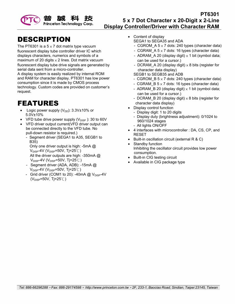
DESCRIPTION The PT6301 is a 5 × 7 dot matrix type vacuum fluorescent display tube controller driver IC which displays characters, numerics and symbols of a maximum of 20 digits × 2 lines. Dot matrix vacuum fluorescent display tube drive signals are generated by serial data sent from a micro-controller. A display system is easily realized by internal ROM and RAM for character display. PT6301 has low power consumption since it is made by CMOS process technology. Custom codes are provided on customer’s request.
FEATURES • Logic power supply (VDD): 3.3V±10% or
5.0V±10% • VFD tube drive power supply (VDISP ): 30 to 60V • VFD driver output current(VFD driver output can
be connected directly to the VFD tube. No pull-down resistor is required.) - Segment driver (SEGA1 to A35, SEGB1 to
B35) Only one driver output is high: -5mA @ VDISP-4V (VDISP=50V, Tj=25)
All the driver outputs are high: -350mA @ VDISP-4V (VDISP=50V, Tj=25)
- Segment driver (ADA, ADB): -15mA @ VDISP-4V (VDISP=50V, Tj=25)
- Grid driver (COM1 to 20): -40mA @ VDISP-4V (VDISP=50V, Tj=25)
• Content of display SEGA1 to SEGA35 and ADA - CGROM_A 5 × 7 dots: 240 types (character data)- CGRAM_A 5 × 7 dots: 16 types (character data) - ADRAM_A 20 (display digit) × 1 bit (symbol data;
can be used for a cursor.) - DCRAM_A 20 (display digit) × 8 bits (register for
character data display) SEGB1 to SEGB35 and ADB - CGROM_B 5 × 7 dots: 240 types (character data)- CGRAM_B 5 × 7 dots: 16 types (character data) - ADRAM_B 20 (display digit) × 1 bit (symbol data;
can be used for a cursor.) - DCRAM_B 20 (display digit) × 8 bits (register for character data display)
• Display control function - Display digit: 1 to 20 digits - Display duty (brightness adjustment): 0/1024 to
960/1024 stages - All lights ON/OFF
• 4 interfaces with microcontroller : DA, CS, CP, and RESET
• Built-in oscillation circuit (external R & C) • Standby function
Inhibiting the oscillator circuit provides low power consumption.
• Built-in CIG testing circuit • Available in CIG package type
PT6301
V1.2 2 March 2012
BLOCK DIAGRAM

PT6301
V1.2 3 March 2012
APPLICATION CIRCUIT
Notes: *1. The VDISP voltage depends on the fluorescent display tube used. Adjust the value of the constants R2 and ZD to the VDISP voltage used. *2. The value of R1 & C1 depend on PT6301 IC chip Supply voltage of VDD (R1=8.2KΩ, C1=39pF, when VDD=5V; R1=6.2KΩ, C1=39pF, when VDD=3.3V).
PT6301
V1.2 4 March 2012
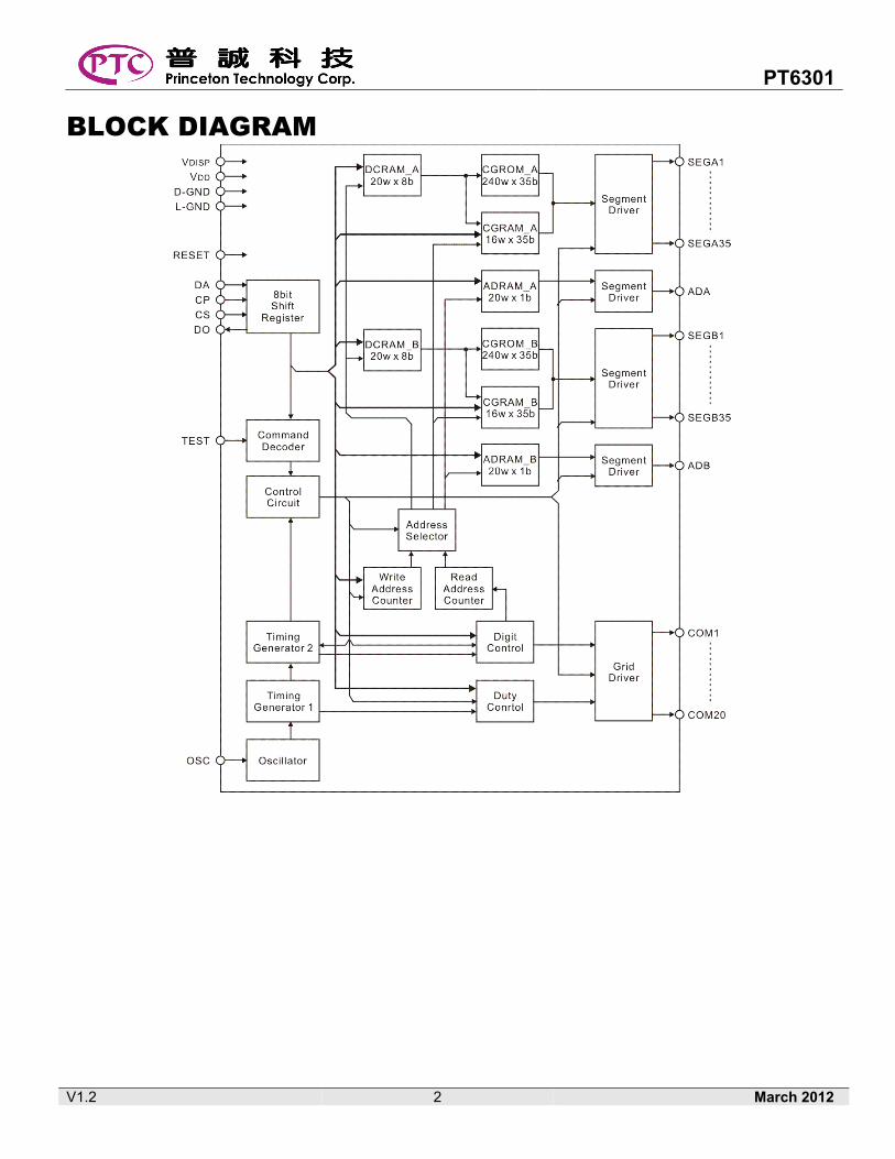
ORDER INFORMATION Valid Part Number Package Type Top Code
PT6301 CIG -
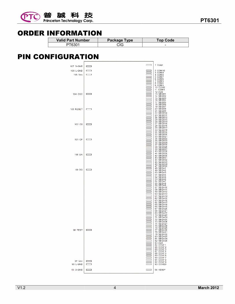
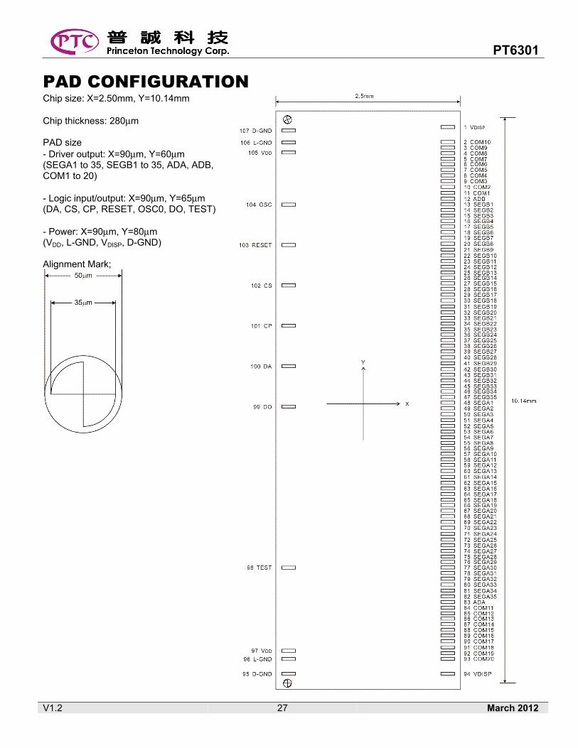
PIN CONFIGURATION
PT6301
V1.2 5 March 2012
PIN DESCRIPTION Pin Name I/O Description Pin No.
SEGA1 ~ SEGA35 O
VFD tube anode electrode drive output. Directly connected to fluorescent display tube and a pulldown resistor is not necessary. IOH > -5mA
48 ~ 82
SEGB1 ~ SEGB35 13 ~ 47
COM1 ~ COM20 O VFD tube grid electrode drive output. Directly connected to fluorescent display tube and a pulldown resistor is not necessary. IOH > -40mA
11 ~ 2, 84 ~ 93
ADA, ADB O VFD tube anode electrode drive output. Directly connected to fluorescent display tube and a pulldown resistor is not necessary. IOH > -15mA
83, 12
VDD
-
VDD, L-GND are power supplies for internal logic. VDISP, D-GND are power supplies for driving fluorescent tubes. Apply VDISP after VDD is applied. Use the same power supply for L-GND and D-GND.
97, 105 L-GND 96, 106 VDISP 1, 94
D-GND 95, 107
TEST I Test mode control pin “High” → Test mode enable “Low” → Test mode disable
98
DO O Data output pin for testing purpose only 99
DA I Serial data input (positive logic). Input from LSB.
100
CP I Shift clock input. Serial data is shifted on the rising edge of CP.
101
CS I Chip select input. Serial data transfer is disabled when CS pin is “H” level.
102
RESET I
Reset input. “Low” initializes all the functions. Initial status is as follows. • Address of each RAM ...address “00”H • Data of each RAM......... Content is undefined • Display digit....................20 digits • Brightness adjustment....0/1024 • All lights ON or OFF ......OFF mode
103
OSC I/O Oscillation connection An oscillator circuit is formed by connecting an external resistor and capacitor at this pin. See Application circuit
104
PT6301
V1.2 6 March 2012
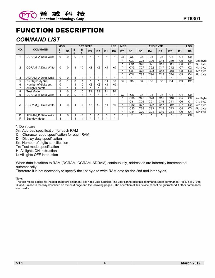
FUNCTION DESCRIPTION COMMAND LIST
NO. COMMAND MSB 1ST BYTE LSB MSB 2ND BYTE LSB B7
B6 B5
B4
B3 B2 B1 B0 B7 B6 B5 B4 B3 B2 B1 B0
1 DCRAM_A Data Write 0 0 0 1 * * * * C7 C6 C5 C4 C3 C2 C1 C0
2 CGRAM_A Data Write 0 0 1 0 X3 X2 X1 X0
* C30 C25 C20 C15 C10 C5 C0 2nd byte* C31 C26 C21 C16 C11 C6 C1 3rd byte* C32 C27 C22 C17 C12 C7 C2 4th byte* C33 C28 C23 C18 C13 C8 C3 5th byte* C34 C29 C24 C19 C14 C9 C4 6th byte
3 ADRAM_A Data Write 0 0 1 1 * * * * * * * * * * * C0 5 Display Duty Set 0 1 0 1 * * D1 D0 D9 D8 D7 D6 D5 D4 D3 D2 6 Number of digits set 0 1 1 0 K3 K2 K1 K0
7 All lights on/off 0 1 1 1 * * H L 8 Test Mode 1 0 0 0 T3 T2 T1 T0 9 DCRAM_B Data Write 1 0 0 1 * * * * C7 C6 C5 C4 C3 C2 C1 C0
A CGRAM_B Data Write 1 0 1 0 X3 X2 X1 X0
* C30 C25 C20 C15 C10 C5 C0 2nd byte* C31 C26 C21 C16 C11 C6 C1 3rd byte* C32 C27 C22 C17 C12 C7 C2 4th byte* C33 C28 C23 C18 C13 C8 C3 5th byte* C34 C29 C24 C19 C14 C9 C4 6th byte
B ADRAM_B Data Write 1 0 1 1 * * * * * * * * * * * C0 F Standby Mode 1 1 1 1 * * * *
*: Don’t care Xn: Address specification for each RAM Cn: Character code specification for each RAM Dn: Display duty specification Kn: Number of digits specification Tn: Test mode specification H: All lights ON instruction L: All lights OFF instruction When data is written to RAM (DCRAM, CGRAM, ADRAM) continuously, addresses are internally incremented automatically. Therefore it is not necessary to specify the 1st byte to write RAM data for the 2nd and later bytes. Note: The test mode is used for inspection before shipment. It is not a user function. The user cannot use this command. Enter commands 1 to 3, 5 to 7, 9 to B, and F alone in the way described on the next page and the following pages. (The operation of this device cannot be guaranteed if other commands are used.)
PT6301
V1.2 7 March 2012
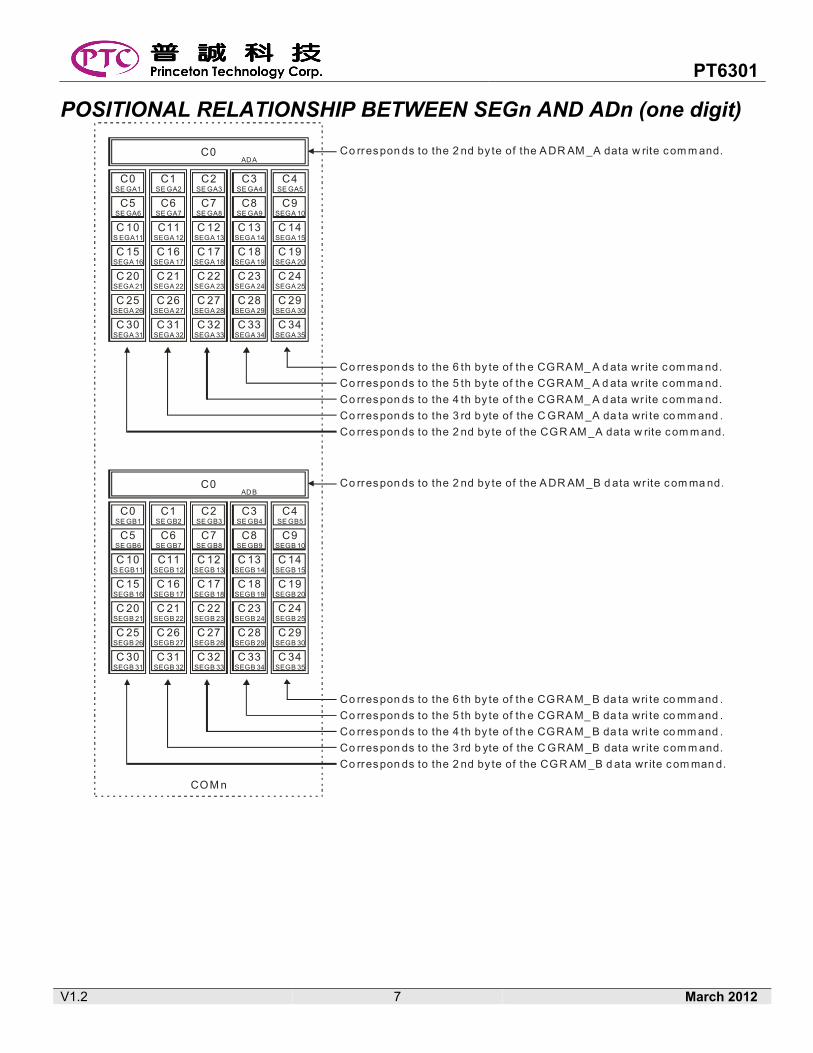
POSITIONAL RELATIONSHIP BETWEEN SEGn AND ADn (one digit)
C0SE GA1
C1SE GA2
C2SE GA3
C3SE GA4
C4SE GA5
C5SE GA6
C6SE GA7
C7SE GA8
C8SE GA9
C9SEGA 10
C 10S EGA11
C11SEGA 12
C 12SEGA 13
C 13SEGA 14
C 14SEGA 15
C 15SEGA 16
C 16SEGA 17
C 17SEGA 18
C 18SEGA 19
C 19SEGA 20
C 20SEGA 21
C 21SEGA 22
C 22SEGA 23
C 23SEGA 24
C 24SEGA 25
C 25SEGA 26
C 26SEGA 27
C 27SEGA 28
C 28SEGA 29
C 29SEGA 30
C 30SEGA 31
C 31SEGA 32
C 32SEGA 33
C 33SEGA 34
C 34SEGA 35
C0ADA
Co rrespon ds to the 2 nd by te of the A DR AM _A data w rite com m and.
Co rrespon ds to the 6 th by te of th e CGRA M_ A d ata wr ite c om ma nd.
Co rrespon ds to the 5 th by te of th e CGRA M_ A d ata wr ite c om ma nd.
Co rrespon ds to the 4 th by te of th e CGRA M_ A d ata wr ite c om ma nd.
Co rrespon ds to the 3 rd b yte of the C GRAM _A da ta wri te co mm and .
Co rrespon ds to the 2 nd by te of the CGR AM _A data w rite com m and.
C0SE GB1
C1SE GB2
C2SE GB3
C3SE GB4
C4SE GB5
C5SE GB6
C6SE GB7
C7SE GB8
C8SE GB9
C9SEGB 10
C 10S EGB11
C11SEGB 12
C 12SEGB 13
C 13SEGB 14
C 14SEGB 15
C 15SEGB 16
C 16SEGB 17
C 17SEGB 18
C 18SEGB 19
C 19SEGB 20
C 20SEGB 21
C 21SEGB 22
C 22SEGB 23
C 23SEGB 24
C 24SEGB 25
C 25SEGB 26
C 26SEGB 27
C 27SEGB 28
C 28SEGB 29
C 29SEGB 30
C 30SEGB 31
C 31SEGB 32
C 32SEGB 33
C 33SEGB 34
C 34SEGB 35
C0ADB
Co rrespon ds to the 2 nd by te of the A DR AM _B d ata wr ite c om ma nd.
Co rrespon ds to the 6 th by te of th e CGRA M_ B da ta wri te co mm and .
Co rrespon ds to the 5 th by te of th e CGRA M_ B da ta wri te co mm and .
Co rrespon ds to the 4 th by te of th e CGRA M_ B da ta wri te co mm and .
Co rrespon ds to the 3 rd b yte of the C GRAM _B data wr ite com m and.
Co rrespon ds to the 2 nd by te of the CGR AM _B d ata wr ite c om man d.
COM n
PT6301
V1.2 8 March 2012
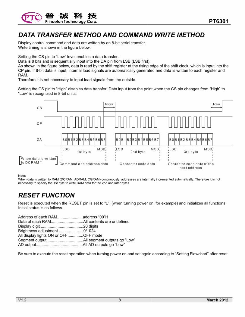
DATA TRANSFER METHOD AND COMMAND WRITE METHOD Display control command and data are written by an 8-bit serial transfer. Write timing is shown in the figure below. Setting the CS pin to “Low” level enables a data transfer. Data is 8 bits and is sequentially input into the DA pin from LSB (LSB first). As shown in the figure below, data is read by the shift register at the rising edge of the shift clock, which is input into the CP pin. If 8-bit data is input, internal load signals are automatically generated and data is written to each register and RAM. Therefore it is not necessary to input load signals from the outside. Setting the CS pin to “High” disables data transfer. Data input from the point when the CS pin changes from “High” to “Low” is recognized in 8-bit units.
Note: When data is written to RAM (DCRAM, ADRAM, CGRAM) continuously, addresses are internally incremented automatically. Therefore it is not necessary to specify the 1st byte to write RAM data for the 2nd and later bytes.
RESET FUNCTION Reset is executed when the RESET pin is set to “L”, (when turning power on, for example) and initializes all functions. Initial status is as follows. Address of each RAM.......................address “00”H Data of each RAM.............................All contents are undefined Display digit ......................................20 digits Brightness adjustment ......................0/1024 All display lights ON or OFF..............OFF mode Segment output.................................All segment outputs go “Low” AD output..........................................All AD outputs go “Low” Be sure to execute the reset operation when turning power on and set again according to “Setting Flowchart” after reset.
B 0 B 1 B 2 B 3 B 4 B 5 B 6 B 7
LS B M SB1s t by te
Co mm and a nd ad dress data
B 0 B 1 B 2 B 3 B 4 B 5 B 6 B 7
LS B M SB2n d by te
Ch arac te r c ode d ata
B 0 B 1 B 2 B 3 B 4 B 5 B 6 B 7
LS B M SB3rd by te
Cha rac ter co de da ta o f th e nex t add re ss
tDOF F tCS H
CS
CP
DA
W he n data is wr ittento DC RAM *
PT6301
V1.2 9 March 2012
DESCRIPTION OF COMMANDS AND FUNCTIONS 1 AND 9. DCRAM DATA WRITE (Write the character code of CGROM and CGRAM to DCRAM) DCRAM (Data Control RAM) has 20 address x 8-bit RAM to store character code of CGROM and CGRAM. Address 00H(0) to 13H(19) corresponds to COM1 to 20. The character code stored in DCRAM is CONVERTED TO A 5 x 7 dot matrix character pattern via CGROM or CGRAM. The DCRAM can store 20 characters. This command writes data from DCRAM address 00H. COMMAND FORMAT MSB LSB
Select DCRAM data write mode (RAM address is set to 00H automatically)
1st Byte (1st)
B7 B6 B5 B4 B3 B2 B1 B0
0/1 0 0 1 * * * * Note: 0: Select DCRAM_A, 1: Select DCRAM_B MSB LSB
Specifies character code of CGRAM and CGROM (written into DCRAM address 00H)
2nd Byte (2nd)
B7 B6 B5 B4 B3 B2 B1 B0
C7 C6 C5 C4 C3 C2 C1 C0 To specify the character code of CGROM and CGRAM continuously to the next address, specify only character code as follows. The address of DCRAM is automatically incremented.
MSB LSB Specifies character code of CGRAM and CGROM (written into DCRAM address 01H)
2nd Byte (3rd)
B7 B6 B5 B4 B3 B2 B1 B0C7 C6 C5 C4 C3 C2 C1 C0
MSB LSB
Specifies character code of CGRAM and CGROM (written into DCRAM address 02H)
2nd Byte (4th)
B7 B6 B5 B4 B3 B2 B1 B0C7 C6 C5 C4 C3 C2 C1 C0
: :
MSB LSB Specifies character code of CGRAM and CGROM (written into DCRAM address 13H)
2nd Byte (21th)
B7 B6 B5 B4 B3 B2 B1 B0
C7 C6 C5 C4 C3 C2 C1 C0
MSB LSB Specifies character code of CGRAM and CGROM (written into DCRAM address 00H)
2nd Byte (22th)
B7 B6 B5 B4 B3 B2 B1 B0C7 C6 C5 C4 C3 C2 C1 C0
C0 (LSB) to C7 (MSB): Character code of CGROM and CGRAM (8 bits 256 characters) *: Don’t care. COM POSITIONS AND DCRAM ADDRESSES
DCRAM address (HEX)
COM position DCRAM address
(HEX) COM position
00H COM1 0AH COM11 01H COM2 0BH COM12 02H COM3 0CH COM13 03H COM4 0DH COM14 04H COM5 0EH COM15 05H COM6 0FH COM16 06H COM7 10H COM17 07H COM8 11H COM18 08H COM9 12H COM19 09H COM10 13H COM20
PT6301
V1.2 10 March 2012
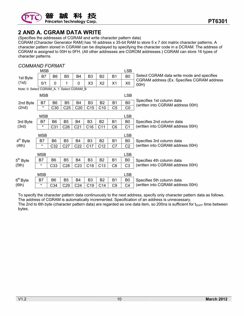
2 AND A. CGRAM DATA WRITE (Specifies the addresses of CGRAM and write character pattern data) CGRAM (Character Generator RAM) has 16 address x 35-bit RAM to store 5 x 7 dot matrix character patterns. A character pattern stored in CGRAM can be displayed by specifying the character code in a DCRAM. The address of CGRAM is assigned to 00H to 0FH. (All other addresses are CGROM addresses.) CGRAM can store 16 types of character patterns. COMMAND FORMAT MSB LSB
Select CGRAM data write mode and specifies CGRAM address (Ex. Specifies CGRAM address 00H)
1st Byte (1st)
B7 B6 B5 B4 B3 B2 B1 B0
0/1 0 1 0 X3 X2 X1 X0 Note: 0: Select CGRAM_A, 1: Select CGRAM_B
MSB LSB Specifies 1st column data (written into CGRAM address 00H) 2nd Byte
(2nd) B7 B6 B5 B4 B3 B2 B1 B0 * C30 C25 C20 C15 C10 C5 C0
MSB LSB
Specifies 2nd column data (written into CGRAM address 00H)
3rd Byte (3rd)
B7 B6 B5 B4 B3 B2 B1 B0 * C31 C26 C21 C16 C11 C6 C1
MSB LSB
Specifies 3rd column data (written into CGRAM address 00H)
4th Byte (4th)
B7 B6 B5 B4 B3 B2 B1 B0 * C32 C27 C22 C17 C12 C7 C2
MSB LSB
Specifies 4th column data (written into CGRAM address 00H)
5th Byte (5th)
B7 B6 B5 B4 B3 B2 B1 B0
* C33 C28 C23 C18 C13 C8 C3
MSB LSB Specifies 5th column data (written into CGRAM address 00H)
6th Byte (6th)
B7 B6 B5 B4 B3 B2 B1 B0 * C34 C29 C24 C19 C14 C9 C4
To specify the character pattern data continuously to the next address, specify only character pattern data as follows. The address of CGRAM is automatically incremented. Specification of an address is unnecessary. The 2nd to 6th byte (character pattern data) are regarded as one data item, so 200ns is sufficient for tDOFF time between bytes.
PT6301
V1.2 11 March 2012
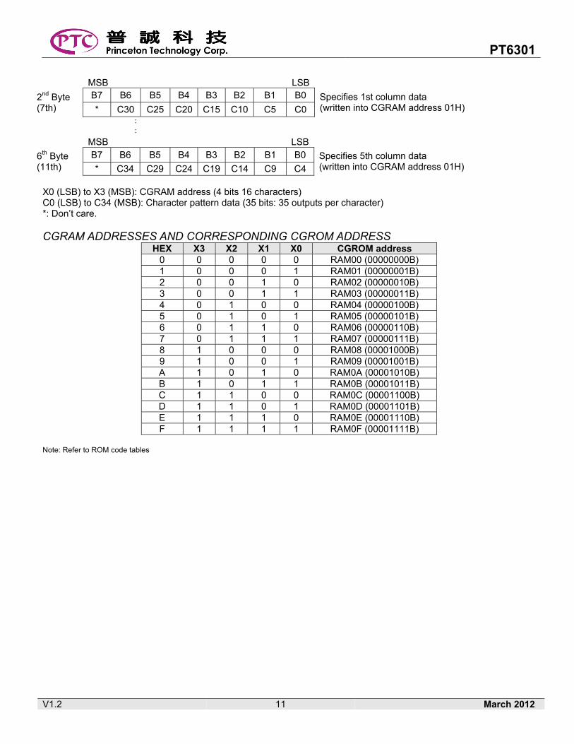
MSB LSB
Specifies 1st column data (written into CGRAM address 01H)
2nd Byte (7th)
B7 B6 B5 B4 B3 B2 B1 B0
* C30 C25 C20 C15 C10 C5 C0 : :
MSB LSB Specifies 5th column data (written into CGRAM address 01H)
6th Byte (11th)
B7 B6 B5 B4 B3 B2 B1 B0
* C34 C29 C24 C19 C14 C9 C4 X0 (LSB) to X3 (MSB): CGRAM address (4 bits 16 characters) C0 (LSB) to C34 (MSB): Character pattern data (35 bits: 35 outputs per character) *: Don’t care. CGRAM ADDRESSES AND CORRESPONDING CGROM ADDRESS
HEX X3 X2 X1 X0 CGROM address 0 0 0 0 0 RAM00 (00000000B) 1 0 0 0 1 RAM01 (00000001B) 2 0 0 1 0 RAM02 (00000010B) 3 0 0 1 1 RAM03 (00000011B) 4 0 1 0 0 RAM04 (00000100B) 5 0 1 0 1 RAM05 (00000101B) 6 0 1 1 0 RAM06 (00000110B) 7 0 1 1 1 RAM07 (00000111B) 8 1 0 0 0 RAM08 (00001000B) 9 1 0 0 1 RAM09 (00001001B) A 1 0 1 0 RAM0A (00001010B) B 1 0 1 1 RAM0B (00001011B) C 1 1 0 0 RAM0C (00001100B) D 1 1 0 1 RAM0D (00001101B) E 1 1 1 0 RAM0E (00001110B) F 1 1 1 1 RAM0F (00001111B)
Note: Refer to ROM code tables
PT6301
V1.2 12 March 2012
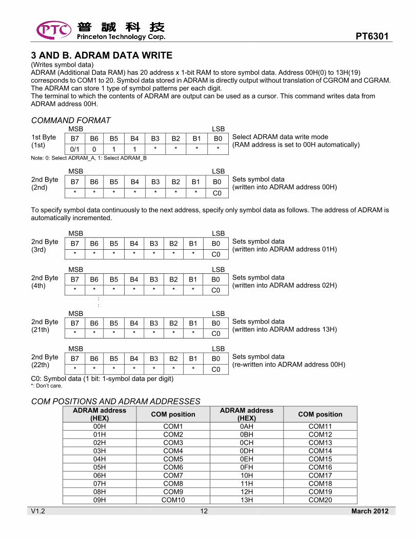
3 AND B. ADRAM DATA WRITE (Writes symbol data) ADRAM (Additional Data RAM) has 20 address x 1-bit RAM to store symbol data. Address 00H(0) to 13H(19) corresponds to COM1 to 20. Symbol data stored in ADRAM is directly output without translation of CGROM and CGRAM. The ADRAM can store 1 type of symbol patterns per each digit. The terminal to which the contents of ADRAM are output can be used as a cursor. This command writes data from ADRAM address 00H. COMMAND FORMAT MSB LSB
Select ADRAM data write mode (RAM address is set to 00H automatically)
1st Byte (1st)
B7 B6 B5 B4 B3 B2 B1 B0
0/1 0 1 1 * * * * Note: 0: Select ADRAM_A, 1: Select ADRAM_B MSB LSB
Sets symbol data (written into ADRAM address 00H)
2nd Byte (2nd)
B7 B6 B5 B4 B3 B2 B1 B0
* * * * * * * C0 To specify symbol data continuously to the next address, specify only symbol data as follows. The address of ADRAM is automatically incremented. MSB LSB
Sets symbol data (written into ADRAM address 01H)
2nd Byte (3rd)
B7 B6 B5 B4 B3 B2 B1 B0
* * * * * * * C0 MSB LSB
Sets symbol data (written into ADRAM address 02H)
2nd Byte (4th)
B7 B6 B5 B4 B3 B2 B1 B0
* * * * * * * C0 : : MSB LSB
Sets symbol data (written into ADRAM address 13H)
2nd Byte (21th)
B7 B6 B5 B4 B3 B2 B1 B0
* * * * * * * C0 MSB LSB
Sets symbol data (re-written into ADRAM address 00H)
2nd Byte (22th)
B7 B6 B5 B4 B3 B2 B1 B0
* * * * * * * C0 C0: Symbol data (1 bit: 1-symbol data per digit) *: Don’t care. COM POSITIONS AND ADRAM ADDRESSES
ADRAM address (HEX)
COM position ADRAM address
(HEX) COM position
00H COM1 0AH COM11 01H COM2 0BH COM12 02H COM3 0CH COM13 03H COM4 0DH COM14 04H COM5 0EH COM15 05H COM6 0FH COM16 06H COM7 10H COM17 07H COM8 11H COM18 08H COM9 12H COM19 09H COM10 13H COM20
PT6301
V1.2 13 March 2012
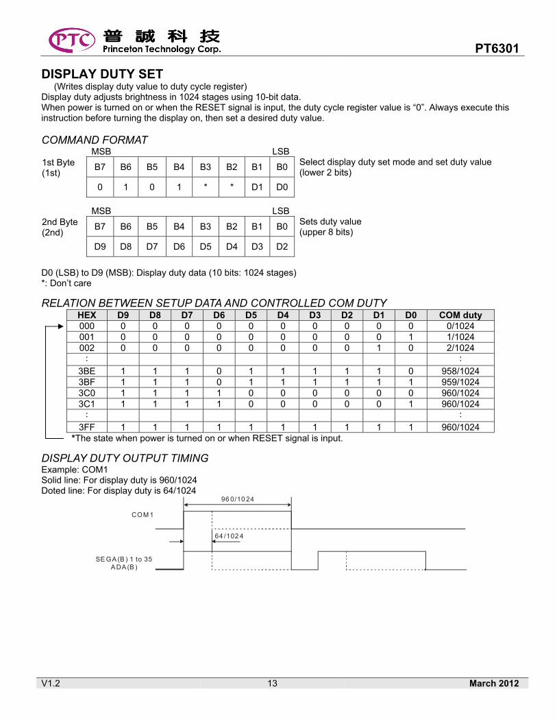
DISPLAY DUTY SET (Writes display duty value to duty cycle register) Display duty adjusts brightness in 1024 stages using 10-bit data. When power is turned on or when the RESET signal is input, the duty cycle register value is “0”. Always execute this instruction before turning the display on, then set a desired duty value. COMMAND FORMAT MSB LSB
Select display duty set mode and set duty value (lower 2 bits)
1st Byte (1st)
B7 B6 B5 B4 B3 B2 B1 B0
0 1 0 1 * * D1 D0
MSB LSB
Sets duty value (upper 8 bits)
2nd Byte (2nd)
B7 B6 B5 B4 B3 B2 B1 B0
D9 D8 D7 D6 D5 D4 D3 D2
D0 (LSB) to D9 (MSB): Display duty data (10 bits: 1024 stages) *: Don’t care
RELATION BETWEEN SETUP DATA AND CONTROLLED COM DUTY HEX D9 D8 D7 D6 D5 D4 D3 D2 D1 D0 COM duty 000 0 0 0 0 0 0 0 0 0 0 0/1024 001 0 0 0 0 0 0 0 0 0 1 1/1024 002 0 0 0 0 0 0 0 0 1 0 2/1024 : :
3BE 1 1 1 0 1 1 1 1 1 0 958/1024 3BF 1 1 1 0 1 1 1 1 1 1 959/1024 3C0 1 1 1 1 0 0 0 0 0 0 960/1024 3C1 1 1 1 1 0 0 0 0 0 1 960/1024 : :
3FF 1 1 1 1 1 1 1 1 1 1 960/1024 *The state when power is turned on or when RESET signal is input.
DISPLAY DUTY OUTPUT TIMING Example: COM1 Solid line: For display duty is 960/1024 Doted line: For display duty is 64/1024
96 0/10 24
64 /102 4
COM 1
SE GA (B ) 1 to 35A DA (B )
PT6301
V1.2 14 March 2012
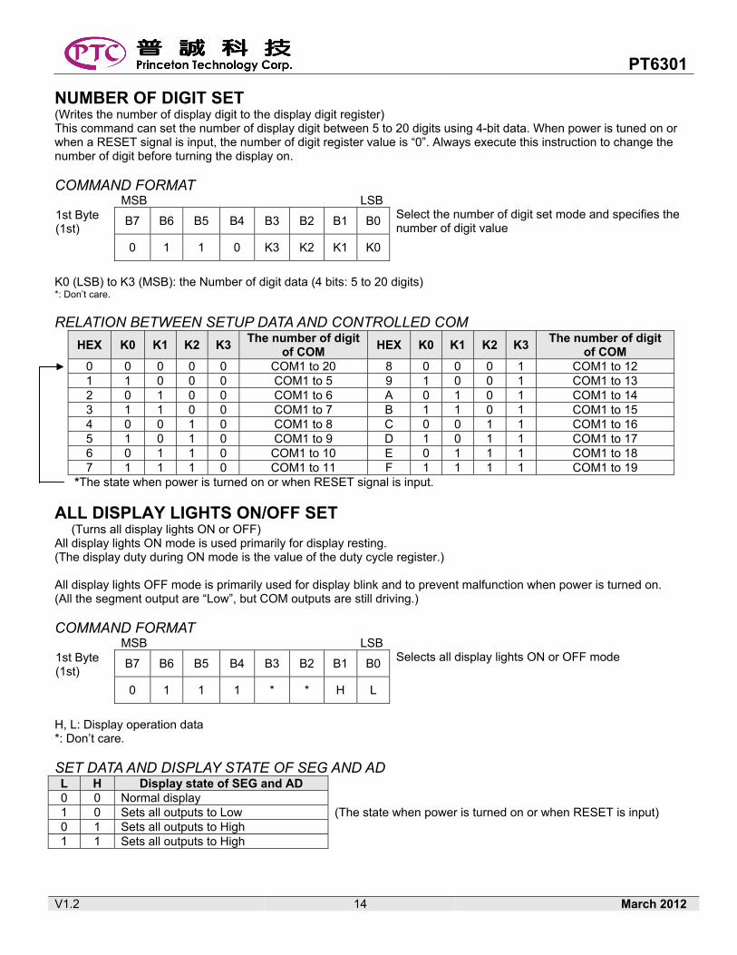
NUMBER OF DIGIT SET (Writes the number of display digit to the display digit register) This command can set the number of display digit between 5 to 20 digits using 4-bit data. When power is tuned on or when a RESET signal is input, the number of digit register value is “0”. Always execute this instruction to change the number of digit before turning the display on. COMMAND FORMAT MSB LSB
Select the number of digit set mode and specifies the number of digit value
1st Byte (1st)
B7 B6 B5 B4 B3 B2 B1 B0
0 1 1 0 K3 K2 K1 K0
K0 (LSB) to K3 (MSB): the Number of digit data (4 bits: 5 to 20 digits) *: Don’t care. RELATION BETWEEN SETUP DATA AND CONTROLLED COM
HEX K0 K1 K2 K3 The number of digit
of COM HEX K0 K1 K2 K3
The number of digit of COM
0 0 0 0 0 COM1 to 20 8 0 0 0 1 COM1 to 12 1 1 0 0 0 COM1 to 5 9 1 0 0 1 COM1 to 13 2 0 1 0 0 COM1 to 6 A 0 1 0 1 COM1 to 14 3 1 1 0 0 COM1 to 7 B 1 1 0 1 COM1 to 15 4 0 0 1 0 COM1 to 8 C 0 0 1 1 COM1 to 16 5 1 0 1 0 COM1 to 9 D 1 0 1 1 COM1 to 17 6 0 1 1 0 COM1 to 10 E 0 1 1 1 COM1 to 18 7 1 1 1 0 COM1 to 11 F 1 1 1 1 COM1 to 19
*The state when power is turned on or when RESET signal is input.
ALL DISPLAY LIGHTS ON/OFF SET (Turns all display lights ON or OFF) All display lights ON mode is used primarily for display resting. (The display duty during ON mode is the value of the duty cycle register.) All display lights OFF mode is primarily used for display blink and to prevent malfunction when power is turned on. (All the segment output are “Low”, but COM outputs are still driving.) COMMAND FORMAT MSB LSB
Selects all display lights ON or OFF mode 1st Byte (1st)
B7 B6 B5 B4 B3 B2 B1 B0
0 1 1 1 * * H L
H, L: Display operation data *: Don’t care. SET DATA AND DISPLAY STATE OF SEG AND AD L H Display state of SEG and AD 0 0 Normal display 1 0 Sets all outputs to Low (The state when power is turned on or when RESET is input) 0 1 Sets all outputs to High 1 1 Sets all outputs to High
PT6301
V1.2 15 March 2012
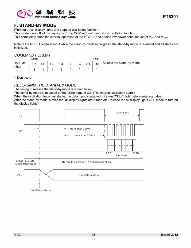
F. STAND-BY MODE (Turning off all display-lights and stopped oscillation function) This mode turns off all display-lights (fixing COM at “Low”) and stops oscillation function. This completely stops the internal operation of the PT6301 and attains low power consumption of VDD and VDISP. Note: If the RESET signal is input while the stand-by mode in progress, the stand-by mode is released and all states are initialized. COMMAND FORMAT MSB LSB
Selects the stand-by mode 1st Byte (1st)
B7 B6 B5 B4 B3 B2 B1 B0
1 1 1 1 * * * *
*: Don’t care. RELEASING THE STAND-BY MODE The timing to release the stand-by mode is shown below. The stand-by mode is released at the falling edge of CS. (The internal oscillation starts) When the oscillation becomes stable, the data input is enabled. (Return CS to “High” before entering data) After the stand-by mode is released, all display-lights are turned off. Release the all display-lights OFF mode to turn on the display-lights.
m ore th an 20 0ns
m ore th an 20 0ns
Sta nd-by sta te(Os ci lla tion s top)
OS C
Osci llati on s tar ts
CS
CP
Da ta inpu t
LS B M SBFirs t by te
No rm all y op eratio n (A ll ou tput are "Low ")
Osci llati on s tate
B0 B1 B2 B3 B4 B5 B6 B7
PT6301
V1.2 16 March 2012
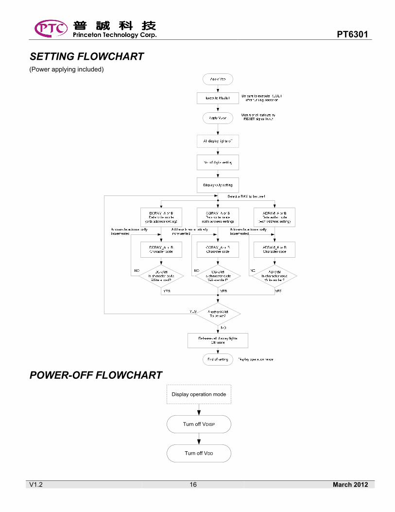
SETTING FLOWCHART (Power applying included)
POWER-OFF FLOWCHART
Display operation mode
Turn off VDISP
Turn off VDD
PT6301
V1.2 17 March 2012
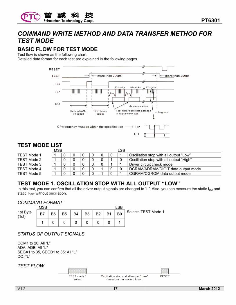
COMMAND WRITE METHOD AND DATA TRANSFER METHOD FOR TEST MODE BASIC FLOW FOR TEST MODE Test flow is shown as the following chart. Detailed data format for each test are explained in the following pages.
TEST MODE LIST MSB LSB TEST Mode 1 1 0 0 0 0 0 0 1 Oscillation stop with all output “Low” TEST Mode 2 1 0 0 0 0 0 1 0 Oscillation stop with all output “High” TEST Mode 3 1 0 0 0 0 0 1 1 Driver circuit check mode TEST Mode 4 1 0 0 0 0 1 0 0 DCRAM/ADRAM/DIGIT data output mode TEST Mode 5 1 0 0 0 0 1 0 1 CGRAM/CGROM data output mode
TEST MODE 1. OSCILLATION STOP WITH ALL OUTPUT “LOW” In this test, you can confirm that all the driver output signals are changed to “L”. Also, you can measure the static IDO and static IDISP without oscillation. COMMAND FORMAT MSB LSB
Selects TEST Mode 1 1st Byte (1st)
B7 B6 B5 B4 B3 B2 B1 B0
1 0 0 0 0 0 0 1
STATUS OF OUTPUT SIGNALS COM1 to 20: All “L” ADA, ADB: All “L” SEGA1 to 35, SEGB1 to 35: All “L” DO: “L” TEST FLOW
PT6301
V1.2 18 March 2012
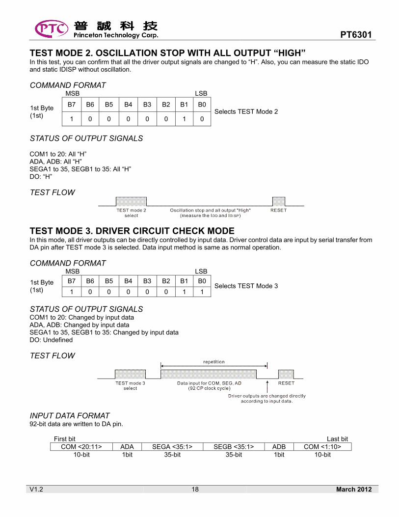
TEST MODE 2. OSCILLATION STOP WITH ALL OUTPUT “HIGH” In this test, you can confirm that all the driver output signals are changed to “H”. Also, you can measure the static IDO and static IDISP without oscillation. COMMAND FORMAT MSB LSB
Selects TEST Mode 2 1st Byte
(1st)
B7 B6 B5 B4 B3 B2 B1 B0
1 0 0 0 0 0 1 0
STATUS OF OUTPUT SIGNALS COM1 to 20: All “H” ADA, ADB: All “H” SEGA1 to 35, SEGB1 to 35: All “H” DO: “H” TEST FLOW
TEST MODE 3. DRIVER CIRCUIT CHECK MODE In this mode, all driver outputs can be directly controlled by input data. Driver control data are input by serial transfer from DA pin after TEST mode 3 is selected. Data input method is same as normal operation. COMMAND FORMAT MSB LSB
Selects TEST Mode 3 1st Byte
(1st) B7 B6 B5 B4 B3 B2 B1 B0
1 0 0 0 0 0 1 1 STATUS OF OUTPUT SIGNALS COM1 to 20: Changed by input data ADA, ADB: Changed by input data SEGA1 to 35, SEGB1 to 35: Changed by input data DO: Undefined TEST FLOW
INPUT DATA FORMAT 92-bit data are written to DA pin.
First bit Last bitCOM <20:11> ADA SEGA <35:1> SEGB <35:1> ADB COM <1:10>
10-bit 1bit 35-bit 35-bit 1bit 10-bit
PT6301
V1.2 19 March 2012
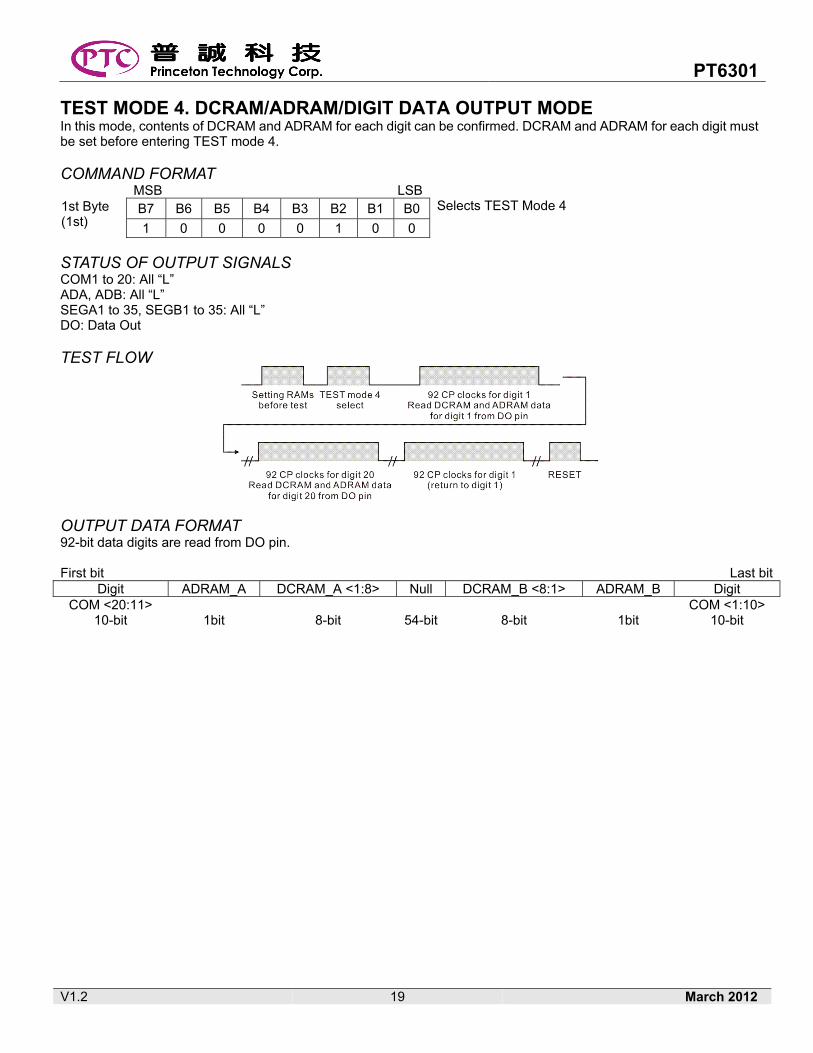
TEST MODE 4. DCRAM/ADRAM/DIGIT DATA OUTPUT MODE In this mode, contents of DCRAM and ADRAM for each digit can be confirmed. DCRAM and ADRAM for each digit must be set before entering TEST mode 4. COMMAND FORMAT MSB LSB
Selects TEST Mode 4 1st Byte (1st)
B7 B6 B5 B4 B3 B2 B1 B0
1 0 0 0 0 1 0 0 STATUS OF OUTPUT SIGNALS COM1 to 20: All “L” ADA, ADB: All “L” SEGA1 to 35, SEGB1 to 35: All “L” DO: Data Out TEST FLOW
OUTPUT DATA FORMAT 92-bit data digits are read from DO pin. First bit Last bit
Digit ADRAM_A DCRAM_A <1:8> Null DCRAM_B <8:1> ADRAM_B Digit COM <20:11> COM <1:10>
10-bit 1bit 8-bit 54-bit 8-bit 1bit 10-bit
PT6301
V1.2 20 March 2012
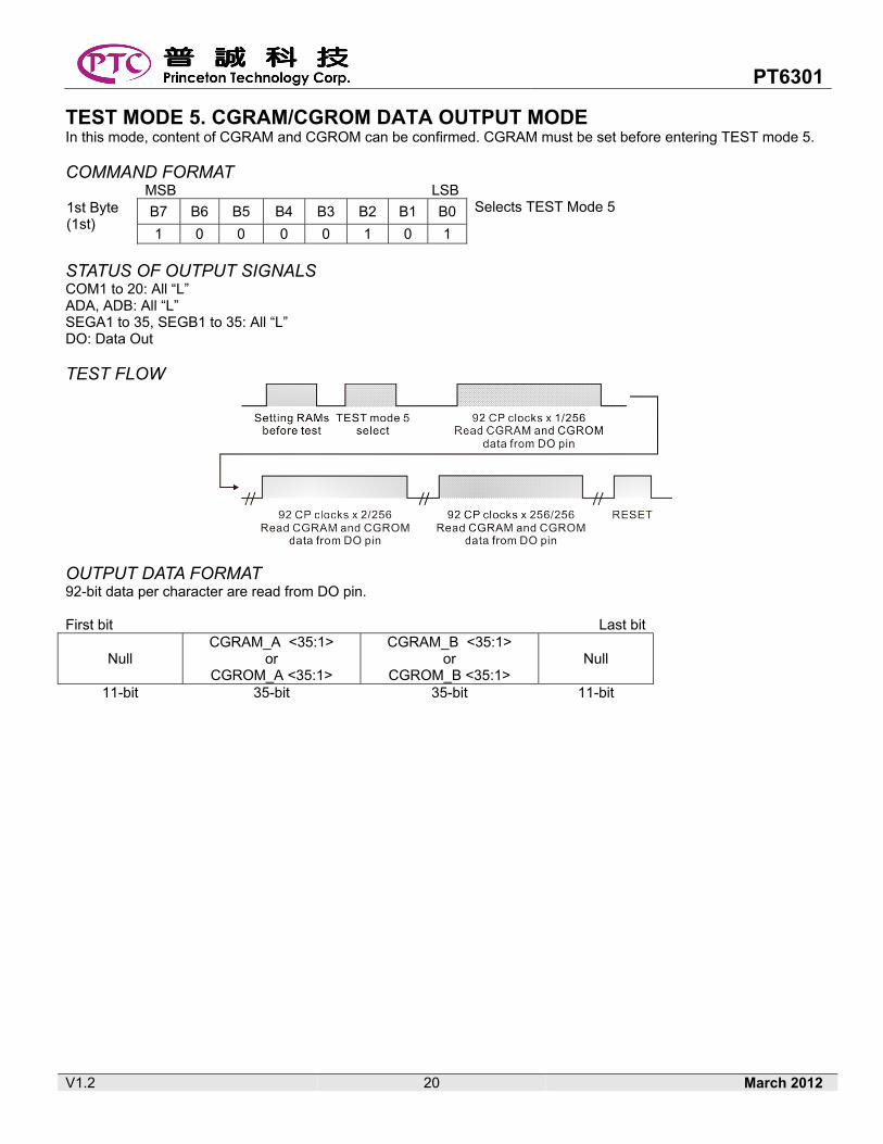
TEST MODE 5. CGRAM/CGROM DATA OUTPUT MODE In this mode, content of CGRAM and CGROM can be confirmed. CGRAM must be set before entering TEST mode 5. COMMAND FORMAT MSB LSB
Selects TEST Mode 5 1st Byte (1st)
B7 B6 B5 B4 B3 B2 B1 B0
1 0 0 0 0 1 0 1 STATUS OF OUTPUT SIGNALS COM1 to 20: All “L” ADA, ADB: All “L” SEGA1 to 35, SEGB1 to 35: All “L” DO: Data Out TEST FLOW
OUTPUT DATA FORMAT 92-bit data per character are read from DO pin. First bit Last bit
Null CGRAM_A <35:1>
or CGROM_A <35:1>
CGRAM_B <35:1> or
CGROM_B <35:1> Null
11-bit 35-bit 35-bit 11-bit
PT6301
V1.2 21 March 2012
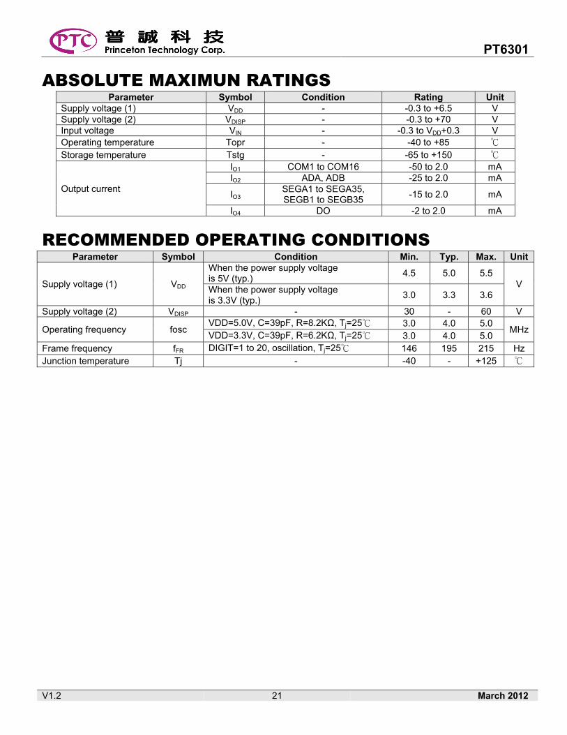
ABSOLUTE MAXIMUN RATINGS Parameter Symbol Condition Rating Unit
Supply voltage (1) VDD - -0.3 to +6.5 V Supply voltage (2) VDISP - -0.3 to +70 V Input voltage VIN - -0.3 to VDD+0.3 V Operating temperature Topr - -40 to +85
Storage temperature Tstg - -65 to +150
Output current
IO1 COM1 to COM16 -50 to 2.0 mA IO2 ADA, ADB -25 to 2.0 mA
IO3 SEGA1 to SEGA35, SEGB1 to SEGB35
-15 to 2.0 mA
IO4 DO -2 to 2.0 mA
RECOMMENDED OPERATING CONDITIONS Parameter Symbol Condition Min. Typ. Max. Unit
Supply voltage (1) VDD
When the power supply voltage is 5V (typ.)
4.5 5.0 5.5 V
When the power supply voltage is 3.3V (typ.)
3.0 3.3 3.6
Supply voltage (2) VDISP - 30 - 60 V
Operating frequency fosc VDD=5.0V, C=39pF, R=8.2KΩ, Tj=25 3.0 4.0 5.0
MHzVDD=3.3V, C=39pF, R=6.2KΩ, Tj=25 3.0 4.0 5.0
Frame frequency fFR DIGIT=1 to 20, oscillation, Tj=25 146 195 215 Hz Junction temperature Tj - -40 - +125
PT6301
V1.2 22 March 2012
DC CHARACTERISTICS (Unless otherwise specified, VDD=5.0V±10%, VDISP=30 to 60V, Tj=-40 to +125)
Parameter Symbol Applied Pin Condition Min. Typ. Max. UnitHigh level input voltage
VIH *1 - 0.8VDD - - V
Low level input voltage
VIL *1 - - - 0.2VDD V
High level input current
IIH *1 VDO=VIN=5.0V -1.0 - +1.0 μA
Low level input current
IIL *1 VDO=5.0V, VIN=0.0V -1.0 - +1.0 μA
High level output voltage
VOH1 COM1 to 20 VDISP=50V, IOH1=-40mA, Tj=25 VDISP-4 - - V VOH2 ADA, ADB VDISP=50V, IOH2=-15mA, Tj=25 VDISP-4 - - V
VOH3 SEGA1 to 35,SEGB1 to 35
VDISP=50V, IOH3=-5mA, Tj=25 VDISP-4 - - V
VOH4 DO VDD=5.0V, IOH4=-400μA VDD-0.3 - - V Low level output voltage
VOL1 *2 VDISP=50V, IOL1=+1mA,Tj=25 - - 2.0 V VOL2 DO VDD=5.0V, IOL2=+400μA - - 0.3 V
Current consumption (1)
IDO1 VDD VDD=5.0V, fosc=4.0MHz - - 6 mAIDISP1
VDISP fosc=4.0MHz,
no load
All output lights on - - 1 mA
IDISP2 All output lights off
(Typ: Tj=25) (Max. Tj=85)
- 1.0 15.0 μA
Current consumption (2)
IDD VDD Stand-by mode (Typ.: Tj=25) (Max. Tj=85)
- 1.0 1.0 μA
IDISP VDISP - 1.0 10.0 μA
(Unless otherwise specified, VDD=3.3V±10%, VDISP=30 to 60V, Tj=-40 to +125)
Parameter Symbol Applied Pin Condition Min. Typ. Max. UnitHigh level input voltage
VIH *1 - 0.8VDD - - V
Low level input voltage
VIL *1 - - - 0.2VDD V
High level input current
IIH *1 VDO=VIN=3.3V -1.0 - +1.0 μA
Low level input current
IIL *1 VDO=3.3V, VIN=0.0V -1.0 - +1.0 μA
High level output voltage
VOH1 COM1 to 20 VDISP=50V, IOH1=-40mA, Tj=25 VDISP-4 - - V VOH2 ADA, ADB VDISP=50V, IOH2=-15mA, Tj=25 VDISP-4 - - V
VOH3 SEGA1 to 35, SEGB1 to 35
VDISP=50V, IOH3=-5mA, Tj=25 VDISP-4 - - V
VOH4 DO VDD=3.3V, IOH4=-400μA VDD-0.3 - - V Low level output voltage
VOL1 *2 VDISP=50V, IOL1=+1mA,Tj=25 - - 2.0 V VOL2 DO VDD=3.3V, IOL2=+400μA - - 0.3 V
Current consumption (1)
IDO1 VDD VDD=3.3V, fosc=4.0MHz - - 4 mA
IDISP1
VDISP fosc=4.0MHz
no load
All output lights on - - 1 mA
IDISP2 All output lights off
(Typ: Tj=25) (Max. Tj=85)
- 1.0 15.0 μA
Current consumption (2)
IDD VDD Stand-by mode (Typ.: Tj=25) (Max. Tj=85)
- 1.0 1.0 μA
IDISP VDISP - 1.0 10.0 μA
Notes: 1. *1=CS, CP, DA, RESET 2. *2=SEGA1 to 35, SEGB1 to 35, ADA, ADB, COM1 to 20
PT6301
V1.2 23 March 2012
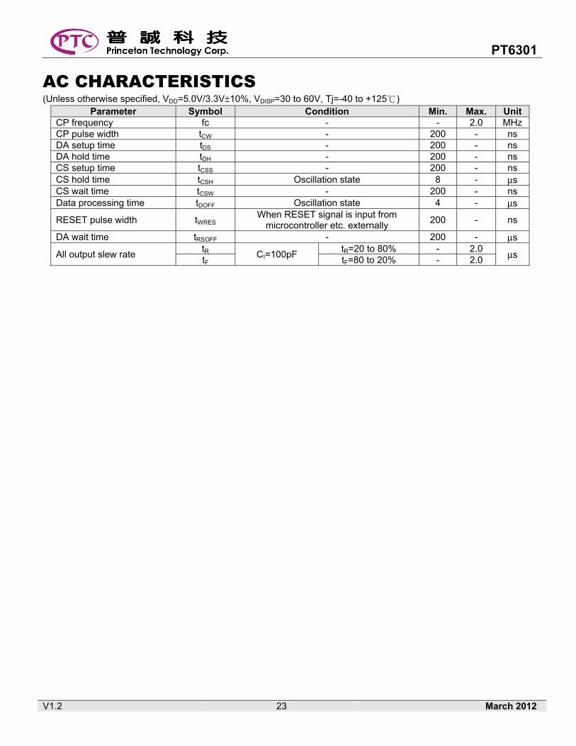
AC CHARACTERISTICS (Unless otherwise specified, VDD=5.0V/3.3V±10%, VDISP=30 to 60V, Tj=-40 to +125)
Parameter Symbol Condition Min. Max. UnitCP frequency fc - - 2.0 MHzCP pulse width tCW - 200 - ns DA setup time tDS - 200 - ns DA hold time tDH - 200 - ns CS setup time tCSS - 200 - ns CS hold time tCSH Oscillation state 8 - μs CS wait time tCSW - 200 - ns Data processing time tDOFF Oscillation state 4 - μs
RESET pulse width tWRES When RESET signal is input from
microcontroller etc. externally 200 - ns
DA wait time tRSOFF - 200 - μs
All output slew rate tR
CI=100pF tR=20 to 80% - 2.0 μs
tF tF=80 to 20% - 2.0
PT6301
V1.2 24 March 2012
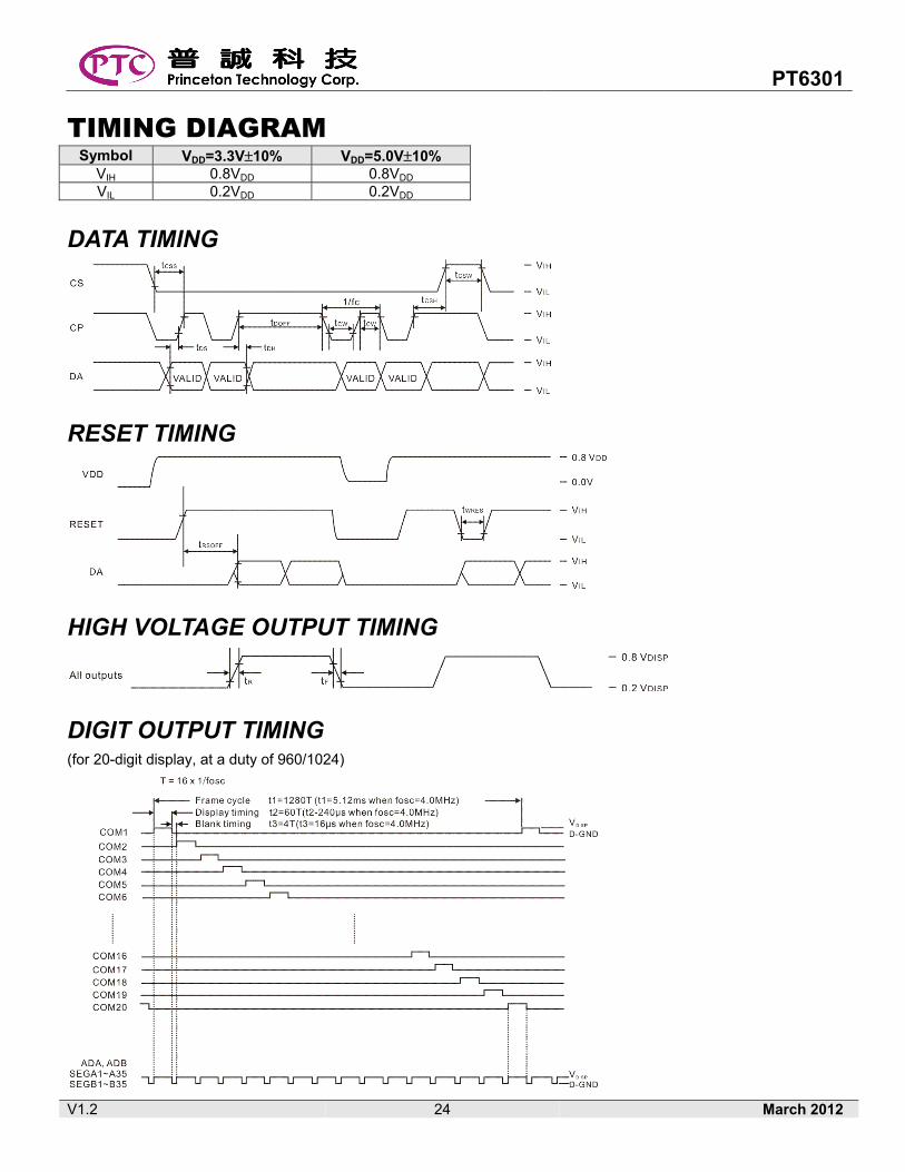
TIMING DIAGRAM Symbol VDD=3.3V±10% VDD=5.0V±10%
VIH 0.8VDD 0.8VDD VIL 0.2VDD 0.2VDD
DATA TIMING
RESET TIMING
HIGH VOLTAGE OUTPUT TIMING
DIGIT OUTPUT TIMING (for 20-digit display, at a duty of 960/1024)
PT6301
V1.2 25 March 2012
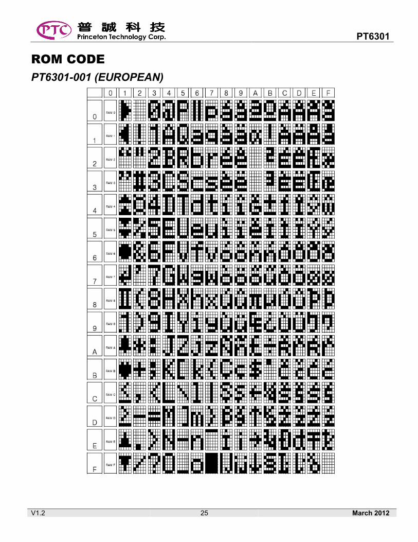
ROM CODE PT6301-001 (EUROPEAN)
PT6301
V1.2 26 March 2012
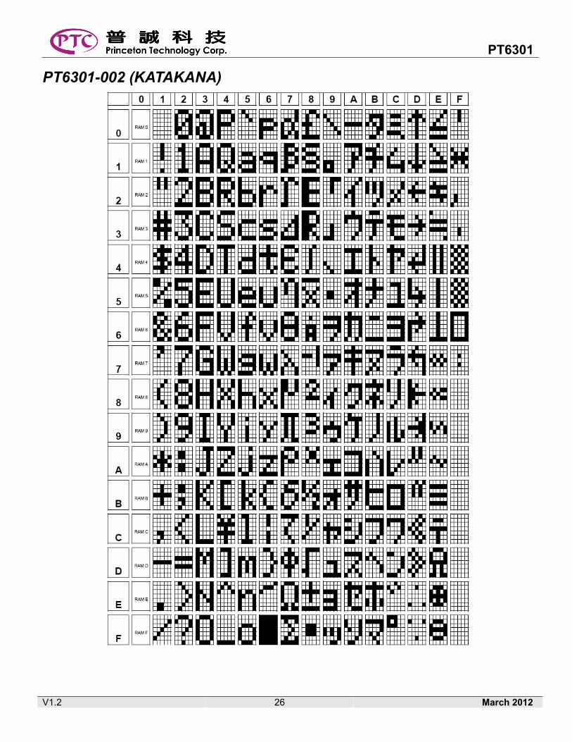
PT6301-002 (KATAKANA)
PT6301
V1.2 27 March 2012
PAD CONFIGURATION Chip size: X=2.50mm, Y=10.14mm Chip thickness: 280μm PAD size - Driver output: X=90μm, Y=60μm (SEGA1 to 35, SEGB1 to 35, ADA, ADB, COM1 to 20) - Logic input/output: X=90μm, Y=65μm (DA, CS, CP, RESET, OSC0, DO, TEST) - Power: X=90μm, Y=80μm (VDD, L-GND, VDISP, D-GND) Alignment Mark;
PT6301
V1.2 28 March 2012
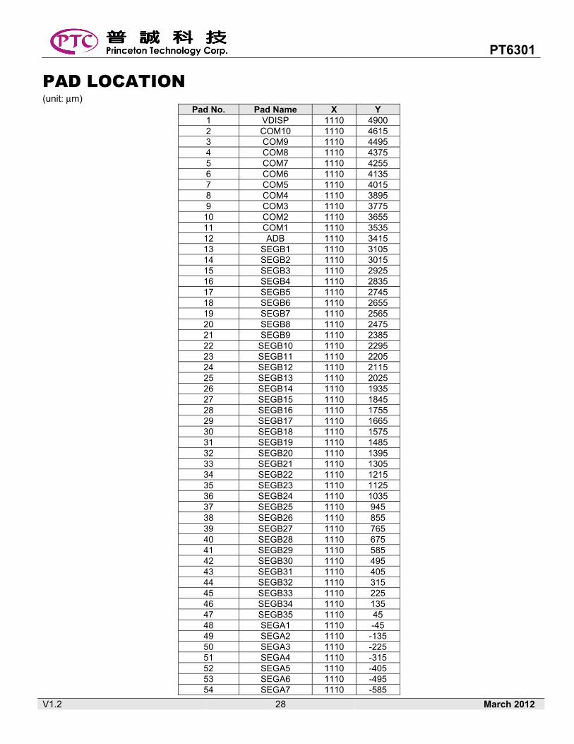
PAD LOCATION (unit: μm)
Pad No. Pad Name X Y 1 VDISP 1110 4900 2 COM10 1110 4615 3 COM9 1110 4495 4 COM8 1110 4375 5 COM7 1110 4255 6 COM6 1110 4135 7 COM5 1110 4015 8 COM4 1110 3895 9 COM3 1110 3775
10 COM2 1110 3655 11 COM1 1110 3535 12 ADB 1110 3415 13 SEGB1 1110 3105 14 SEGB2 1110 3015 15 SEGB3 1110 2925 16 SEGB4 1110 2835 17 SEGB5 1110 2745 18 SEGB6 1110 2655 19 SEGB7 1110 2565 20 SEGB8 1110 2475 21 SEGB9 1110 2385 22 SEGB10 1110 2295 23 SEGB11 1110 2205 24 SEGB12 1110 2115 25 SEGB13 1110 2025 26 SEGB14 1110 1935 27 SEGB15 1110 1845 28 SEGB16 1110 1755 29 SEGB17 1110 1665 30 SEGB18 1110 1575 31 SEGB19 1110 1485 32 SEGB20 1110 1395 33 SEGB21 1110 1305 34 SEGB22 1110 1215 35 SEGB23 1110 1125 36 SEGB24 1110 1035 37 SEGB25 1110 945 38 SEGB26 1110 855 39 SEGB27 1110 765 40 SEGB28 1110 675 41 SEGB29 1110 585 42 SEGB30 1110 495 43 SEGB31 1110 405 44 SEGB32 1110 315 45 SEGB33 1110 225 46 SEGB34 1110 135 47 SEGB35 1110 45 48 SEGA1 1110 -45 49 SEGA2 1110 -135 50 SEGA3 1110 -225 51 SEGA4 1110 -315 52 SEGA5 1110 -405 53 SEGA6 1110 -495 54 SEGA7 1110 -585
PT6301
V1.2 29 March 2012
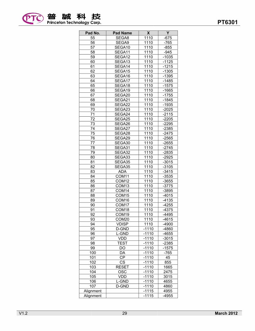
Pad No. Pad Name X Y 55 SEGA8 1110 -675 56 SEGA9 1110 -765 57 SEGA10 1110 -855 58 SEGA11 1110 -945 59 SEGA12 1110 -1035 60 SEGA13 1110 -1125 61 SEGA14 1110 -1215 62 SEGA15 1110 -1305 63 SEGA16 1110 -1395 64 SEGA17 1110 -1485 65 SEGA18 1110 -1575 66 SEGA19 1110 -1665 67 SEGA20 1110 -1755 68 SEGA21 1110 -1845 69 SEGA22 1110 -1935 70 SEGA23 1110 -2025 71 SEGA24 1110 -2115 72 SEGA25 1110 -2205 73 SEGA26 1110 -2295 74 SEGA27 1110 -2385 75 SEGA28 1110 -2475 76 SEGA29 1110 -2565 77 SEGA30 1110 -2655 78 SEGA31 1110 -2745 79 SEGA32 1110 -2835 80 SEGA33 1110 -2925 81 SEGA35 1110 -3015 82 SEGA35 1110 -3105 83 ADA 1110 -3415 84 COM11 1110 -3535 85 COM12 1110 -3655 86 COM13 1110 -3775 87 COM14 1110 -3895 88 COM15 1110 -4015 89 COM16 1110 -4135 90 COM17 1110 -4255 91 COM18 1110 -4375 92 COM19 1110 -4495 93 COM20 1110 -4615 94 VDISP 1110 -4900 95 D-GND -1110 -4860 96 L-GND -1110 -4655 97 VDD -1110 -3015 98 TEST -1110 -2385 99 DO -1110 -1575
100 DA -1110 -765 101 CP -1110 45 102 CS -1110 855 103 RESET -1110 1665 104 OSC -1110 2475 105 VDD -1110 3015 106 L-GND -1110 4655 107 D-GND -1110 4860
Alignment -1115 4955 Alignment -1115 -4955
PT6301
V1.2 30 March 2012
IMPORTANT NOTICE Princeton Technology Corporation (PTC) reserves the right to make corrections, modifications, enhancements, improvements, and other changes to its products and to discontinue any product without notice at any time. PTC cannot assume responsibility for use of any circuitry other than circuitry entirely embodied in a PTC product. No circuit patent licenses are implied. Princeton Technology Corp. 2F, 233-1, Baociao Road, Sindian, Taipei 23145, Taiwan Tel: 886-2-66296288 Fax: 886-2-29174598 http://www.princeton.com.tw
Related Documents
![AKD4425A-SA English Manual - Asahi Kasei Microdevices · AKD4425A-SA has a digital audio interface ... C24 (short) C29 2.2n R21 (short) + C28 (short) R16 470 J1 ... [Read] commands.](https://static.cupdf.com/doc/110x72/5b1b921a7f8b9a28258eb031/akd4425a-sa-english-manual-asahi-kasei-microdevices-akd4425a-sa-has-a-digital.jpg)