DEM 16227 SYH-LY Product Specification 16.08.2017 Display Elektronik GmbH DEM 16227 SYH-LY LCD MODULE Product Specification Version: 2

Welcome message from author
This document is posted to help you gain knowledge. Please leave a comment to let me know what you think about it! Share it to your friends and learn new things together.
Transcript
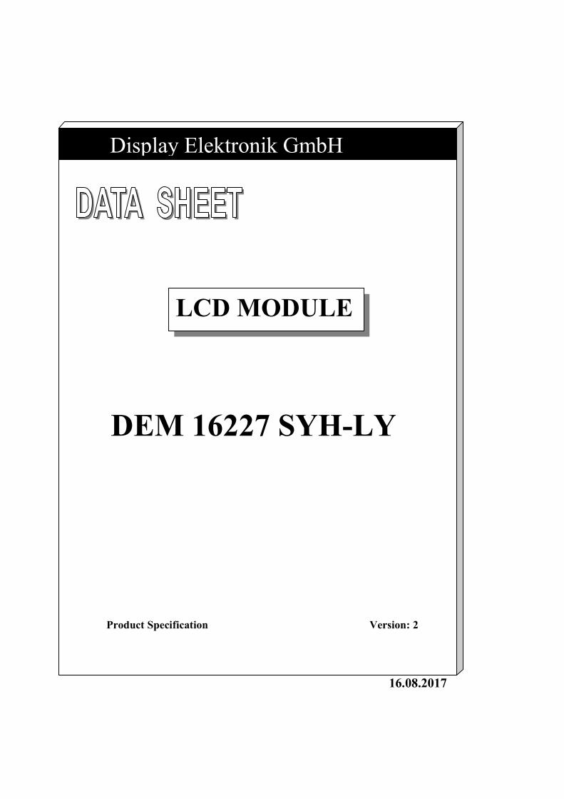
DEM 16227 SYH-LY Product Specification
16.08.2017
Display Elektronik GmbH
DEM 16227 SYH-LY
LCD MODULE
Product Specification Version: 2
DEM 16227 SYH-LY Product Specification
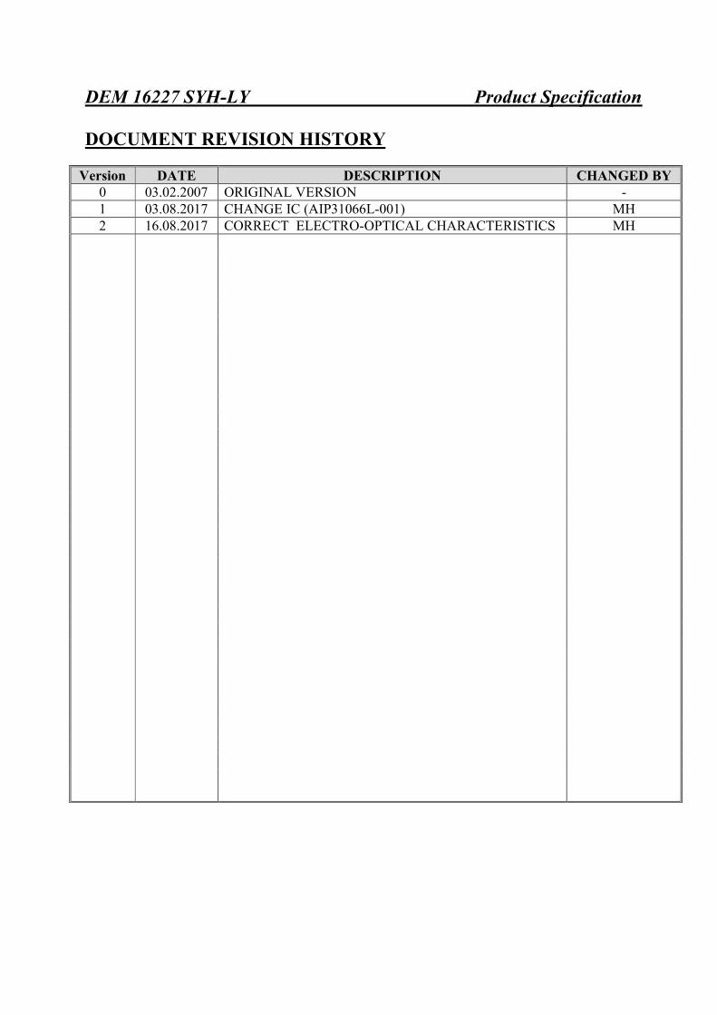
DOCUMENT REVISION HISTORY
Version DATE DESCRIPTION CHANGED BY 0 03.02.2007 ORIGINAL VERSION - 1 03.08.2017 CHANGE IC (AIP31066L-001) MH 2 16.08.2017 CORRECT ELECTRO-OPTICAL CHARACTERISTICS MH
DEM 16227 SYH-LY Product Specification
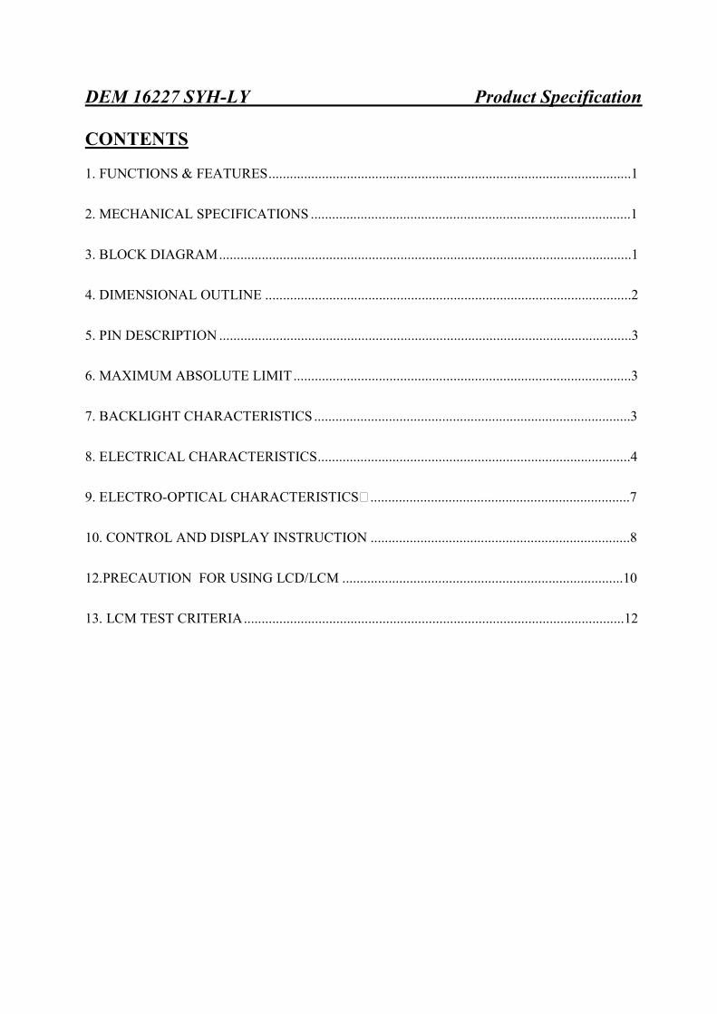
CONTENTS 1. FUNCTIONS & FEATURES ......................................................................................................1
2. MECHANICAL SPECIFICATIONS ..........................................................................................1
3. BLOCK DIAGRAM ....................................................................................................................1
4. DIMENSIONAL OUTLINE .......................................................................................................2
5. PIN DESCRIPTION ....................................................................................................................3
6. MAXIMUM ABSOLUTE LIMIT ...............................................................................................3
7. BACKLIGHT CHARACTERISTICS .........................................................................................3
8. ELECTRICAL CHARACTERISTICS ........................................................................................4
9. ELECTRO-OPTICAL CHARACTERISTICS .........................................................................7
10. CONTROL AND DISPLAY INSTRUCTION .........................................................................8
12.PRECAUTION FOR USING LCD/LCM ...............................................................................10
13. LCM TEST CRITERIA ...........................................................................................................12
DEM 16227 SYH-LY Product Specification
VERSION: 2 PAGE: 1
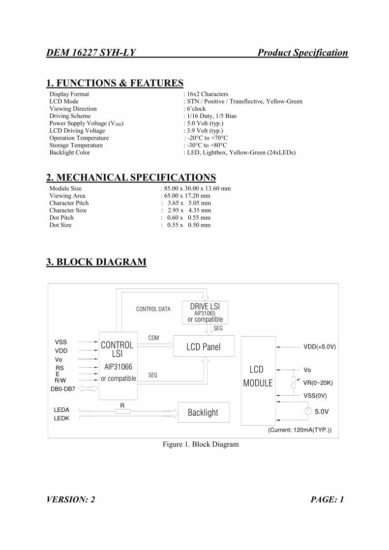
1. FUNCTIONS & FEATURES Display Format : 16x2 Characters LCD Mode : STN / Positive / Transflective, Yellow-Green Viewing Direction : 6’clock Driving Scheme : 1/16 Duty, 1/5 Bias Power Supply Voltage (VDD) : 5.0 Volt (typ.) LCD Driving Voltage : 3.9 Volt (typ.) Operation Temperature : -20°C to +70°C Storage Temperature : -30°C to +80°C Backlight Color : LED, Lightbox, Yellow-Green (24xLEDs)
2. MECHANICAL SPECIFICATIONS Module Size : 85.00 x 30.00 x 13.60 mm Viewing Area : 65.00 x 17.20 mm Character Pitch : 3.65 x 5.05 mm Character Size : 2.95 x 4.35 mm Dot Pitch : 0.60 x 0.55 mm Dot Size : 0.55 x 0.50 mm
3. BLOCK DIAGRAM
5.0V
VoLCD
LCD Panel
MODULEVSS(0V)
VR(0~20K)
VDD(+5.0V)COM
CONTROL DATA
SEG
LSI CONTROL
AIP31066Vo
ERS
LEDK
DB0-DB7
LEDA
R/W
VSSVDD
Backlight
SEG
DRIVE LSIAIP31065
(Current: 120mA(TYP.))
R
or compatible
or compatible
Figure 1. Block Diagram
DEM 16227 SYH-LY Product Specification
VERSION: 2 PAGE: 2
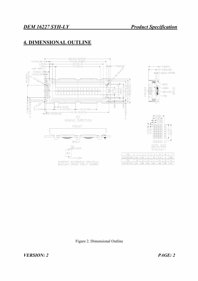
4. DIMENSIONAL OUTLINE
Figure 2. Dimensional Outline
DEM 16227 SYH-LY Product Specification
VERSION: 2 PAGE: 3
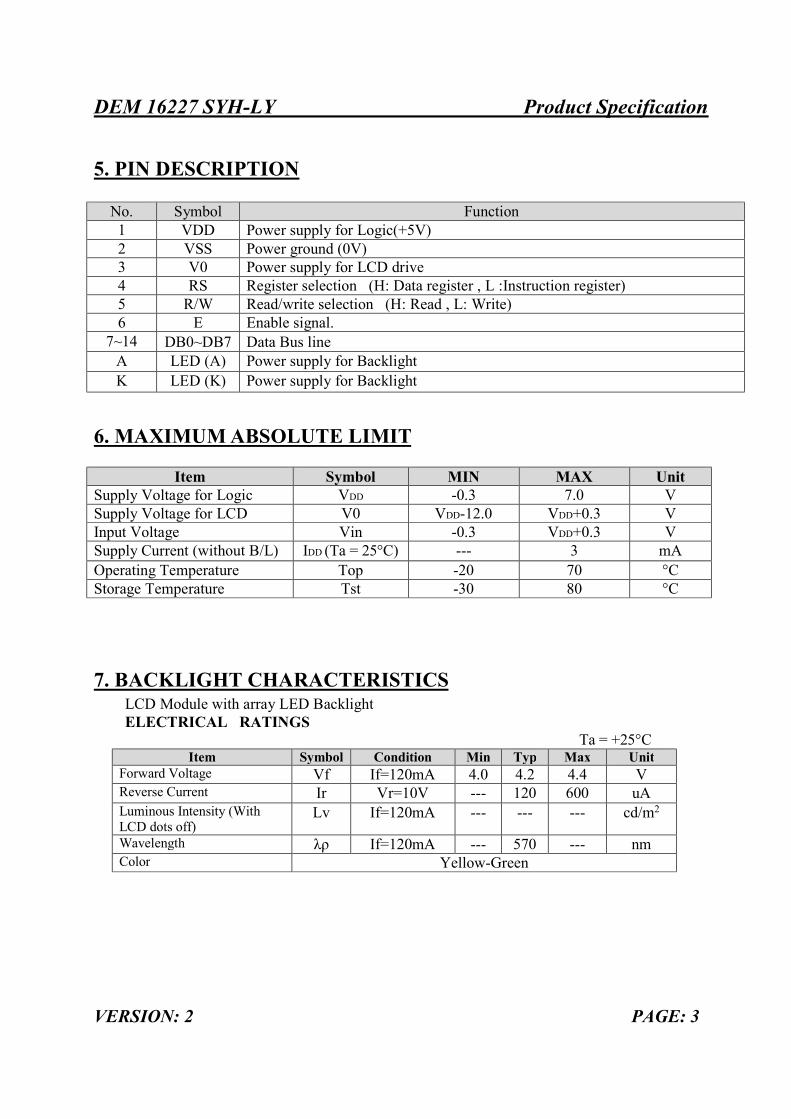
5. PIN DESCRIPTION
No. Symbol Function 1 VDD Power supply for Logic(+5V) 2 VSS Power ground (0V) 3 V0 Power supply for LCD drive 4 RS Register selection (H: Data register , L :Instruction register) 5 R/W Read/write selection (H: Read , L: Write) 6 E Enable signal.
7~14 DB0~DB7 Data Bus line A LED (A) Power supply for Backlight K LED (K) Power supply for Backlight
6. MAXIMUM ABSOLUTE LIMIT
Item Symbol MIN MAX Unit Supply Voltage for Logic VDD -0.3 7.0 V Supply Voltage for LCD V0 VDD-12.0 VDD+0.3 V Input Voltage Vin -0.3 VDD+0.3 V Supply Current (without B/L) IDD (Ta = 25°C) --- 3 mA Operating Temperature Top -20 70 °C Storage Temperature Tst -30 80 °C
7. BACKLIGHT CHARACTERISTICS LCD Module with array LED Backlight ELECTRICAL RATINGS
Ta = +25°C Item Symbol Condition Min Typ Max Unit
Forward Voltage Vf If=120mA 4.0 4.2 4.4 V Reverse Current Ir Vr=10V --- 120 600 uA Luminous Intensity (With LCD dots off)
Lv If=120mA --- --- --- cd/m2
Wavelength λρ If=120mA --- 570 --- nm Color Yellow-Green
DEM 16227 SYH-LY Product Specification
VERSION: 2 PAGE: 4
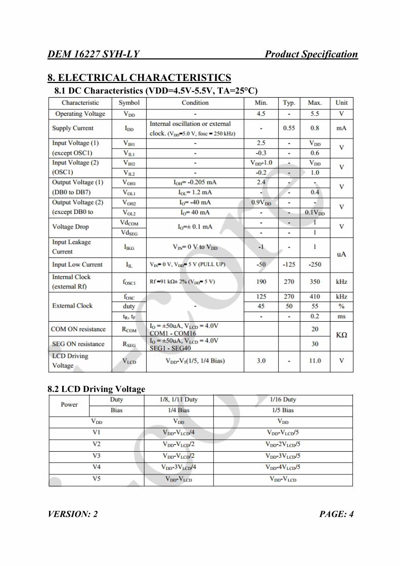
8. ELECTRICAL CHARACTERISTICS 8.1 DC Characteristics (VDD=4.5V-5.5V, TA=25°C)
8.2 LCD Driving Voltage
DEM 16227 SYH-LY Product Specification
VERSION: 2 PAGE: 5
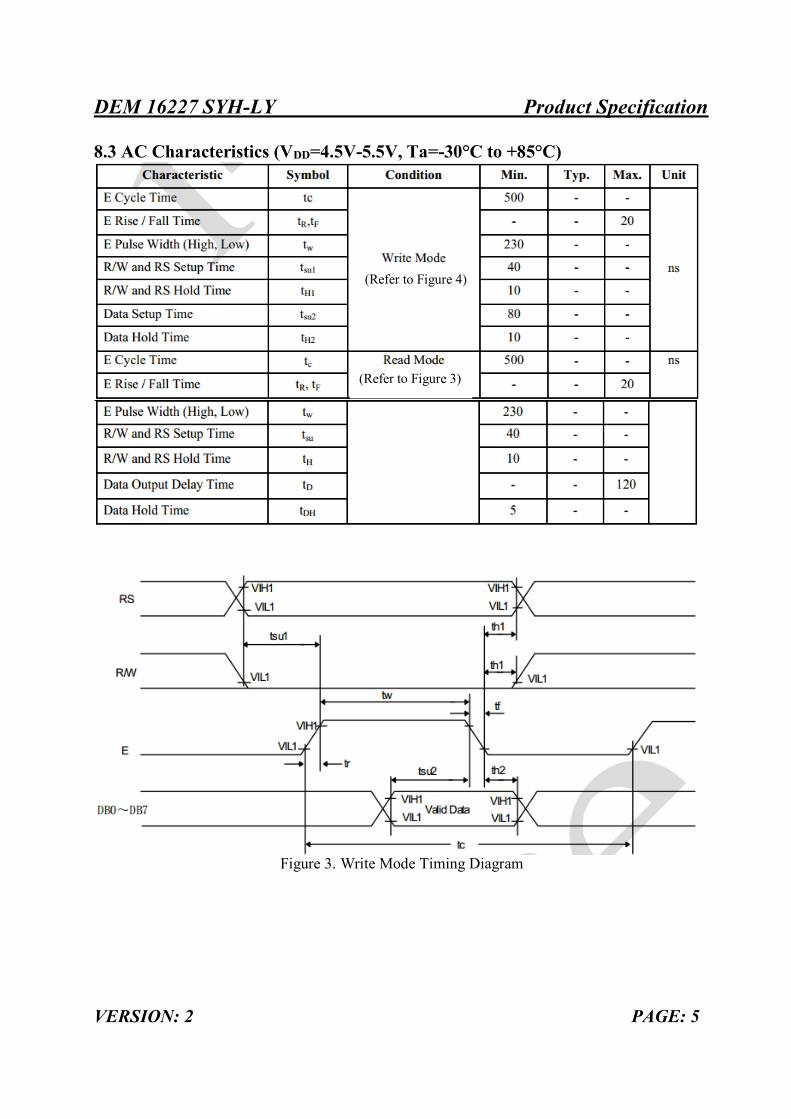
8.3 AC Characteristics (VDD=4.5V-5.5V, Ta=-30°C to +85°C)
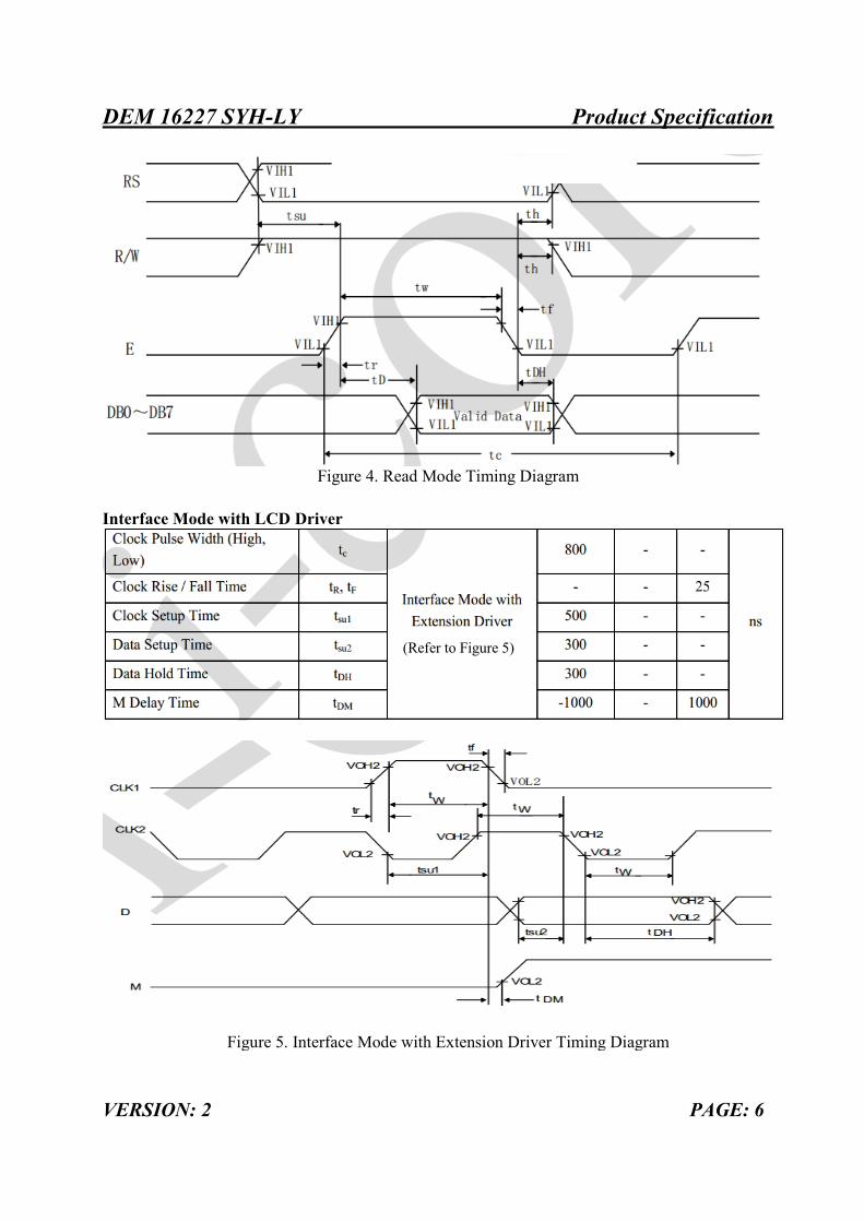
Figure 3. Write Mode Timing Diagram
(Refer to Figure 3)
(Refer to Figure 4)
DEM 16227 SYH-LY Product Specification
VERSION: 2 PAGE: 6
Figure 4. Read Mode Timing Diagram Interface Mode with LCD Driver
Figure 5. Interface Mode with Extension Driver Timing Diagram
(Refer to Figure 5)
DEM 16227 SYH-LY Product Specification
VERSION: 2 PAGE: 7
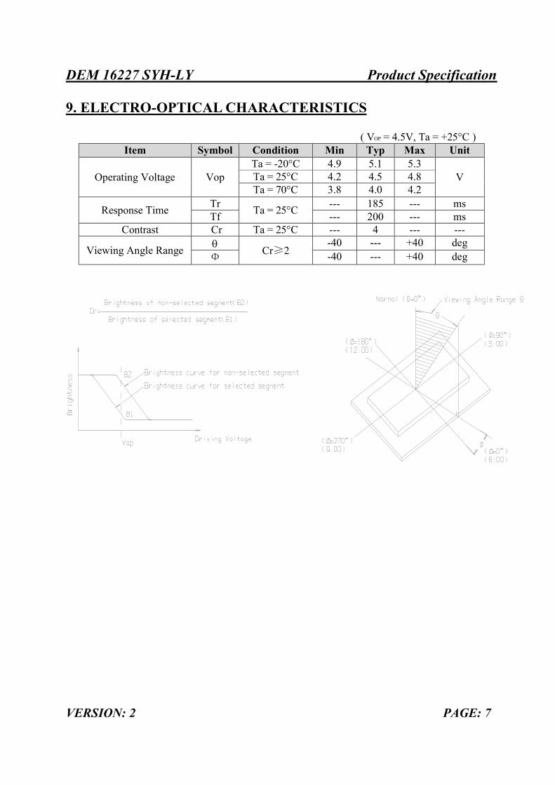
9. ELECTRO-OPTICAL CHARACTERISTICS ( VOP = 4.5V, Ta = +25°C )
Item Symbol Condition Min Typ Max Unit
Operating Voltage
Vop
Ta = -20°C 4.9 5.1 5.3 V Ta = 25°C 4.2 4.5 4.8
Ta = 70°C 3.8 4.0 4.2
Response Time Tr Ta = 25°C --- 185 --- ms Tf --- 200 --- ms
Contrast Cr Ta = 25°C --- 4 --- ---
Viewing Angle Range θ Cr≥2 -40 --- +40 deg
Ф -40 --- +40 deg
DEM 16227 SYH-LY Product Specification
VERSION: 2 PAGE: 8
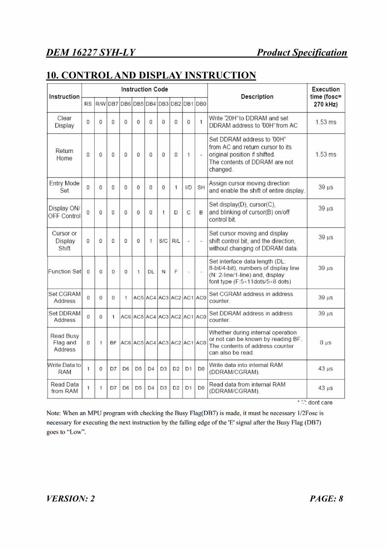
10. CONTROL AND DISPLAY INSTRUCTION
DEM 16227 SYH-LY Product Specification
VERSION: 2 PAGE: 9
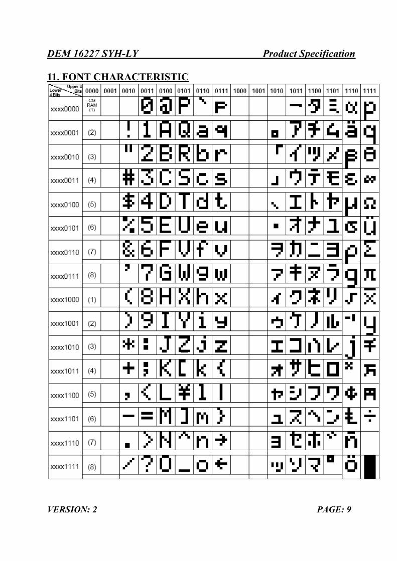
11. FONT CHARACTERISTIC
DEM 16227 SYH-LY Product Specification
VERSION: 2 PAGE: 10
12. PRECAUTION FOR USING LCD/LCM LCD/LCM is assembled and adjusted with a high degree of precision. Do not attempt to make any alteration or modification. The followings should be noted.
General Precautions: l LCD panel is made of glass. Avoid excessive mechanical shock or applying strong pressure
onto the surface of display area. l The polarizer used on the display surface is easily scratched and damaged. Extreme care
should be taken when handling. To clean dust or dirt off the display surface, wipe gently with cotton, or other soft material soaked with isopropyl alcohol or ethyl alcohol, do not use water, ketone or aromatics and never scrub hard.
l Do not tamper in any way with the tabs on the metal frame. l Do not made any modification on the PCB without consulting DISPLAY. l When mounting a LCM, make sure that the PCB is not under any stress such as bending or
twisting. Elastomer contacts are very delicate and missing pixels could result from slight dislocation of any of the elements.
l Avoid pressing on the metal bezel, otherwise the elastomer connector could be deformed and lose contact, resulting in missing pixels and also cause rainbow on the display.
l Be careful not to touch or swallow liquid crystal that might leak from a damaged cell. Any liquid crystal adheres to skin or clothes, wash it off immediately with soap and water.
Static Electricity Precautions:
7. CMOS-LSI is used for the module circuit; therefore operators should be grounded whenever he/she comes into contact with the module.
8. Do not touch any of the conductive parts such as the LSI pads; the copper leads on the PCB and the interface terminals with any parts of the human body.
9. Do not touch the connection terminals of the display with bare hand; it will cause disconnection or defective insulation of terminals.
10. The modules should be kept in anti-static bags or other containers resistant to static for storage.
11. Only properly grounded soldering irons should be used. 12. If an electric screwdriver is used, it should be grounded and shielded to prevent sparks. 13. The normal static prevention measures should be observed for work clothes and working
benches. 14. Since dry air is inductive to static, a relative humidity of 50-60% is recommended. Soldering Precautions:
1. Soldering should be performed only on the I/O terminals. 2. Use soldering irons with proper grounding and no leakage. 3. Soldering temperature:300±5℃ 4. Soldering time: 2 to 3 second. 5. Use eutectic solder with resin flux filling. 6. If flux is used, the LCD surface should be protected to avoid spattering flux. 7. Flux residue should be removed.
DEM 16227 SYH-LY Product Specification
VERSION: 2 PAGE: 11
Operation Precautions:
1. The viewing angle can be adjusted by varying the LCD driving voltage Vo. 2. Since applied DC voltage causes electro-chemical reactions, which deteriorate the display,
the applied pulse waveform should be a symmetric waveform such that no DC component remains. Be sure to use the specified operating voltage.
3. Driving voltage should be kept within specified range; excess voltage will shorten display life.
4. Response time increases with decrease in temperature. 5. Display color may be affected at temperatures above its operational range. 6. Keep the temperature within the specified range usage and storage. Excessive temperature and humidity could cause polarization degradation, polarizer peel-off or generate bubbles. 7. When storing the LCD modules, avoid exposure to direct sunlight or to the light of
fluorescent lamps. For long-term storage, the temperature should be 0°C~40°C, and the relative humidity should be kept 40%~60%.
Limited Warranty
DISPLAY LCDs and modules are not consumer products, but may be incorporated by DISPLAY’s customers into consumer products or components thereof, DISPLAY does not warrant that its LCDs and components are fit for any such particular purpose. 1. The liability of DISPLAY is limited to repair or replacement on the terms set forth below.
DISPLAY will not be responsible for any subsequent or consequential events or injury or damage to any personnel or user including third party personnel and/or user. Unless otherwise agreed in writing between DISPLAY and the customer, DISPLAY will only replace or repair any of its LCD which is found defective electrically or visually when inspected in accordance with DISPLAY general LCD inspection standard . (Copies available on request)
2. No warranty can be granted if any of the precautions state in handling liquid crystal display above has been disregarded. Broken glass, scratches on polarizer mechanical damages as well as defects that are caused accelerated environment tests are excluded from warranty.
3. In returning the LCD/LCM, they must be properly packaged; there should be detailed description of the failures or defect.
DEM 16227 SYH-LY Product Specification
VERSION: 2 PAGE: 12
13. LCM TEST CRITERIA 1.Objective
The LCM test criteria are set to formalize DISPLAY’s LCM quality standards with reference to those of the customer for inspection, release and acceptance of finished LCM products in order to guarantee the quality required by the customer.
2.Scope The criteria are applicable to all the LCM products manufactured by DISPLAY.
3.Equipments for Inspection
Electrical testing machines, vernier calipers, ampere meter, multi-meter, microscopes, anti-static
wrist straps, finger cots, labels, tri-phase thermal shock chamber, constant temperature and
humidity chamber, high-low temperature experimenting box, refrigerators, constant voltage power
supply (DC) , desk Lamps, etc.
4.Sampling Plan and Reference Standards
4.1.1 Sampling plan: Refer to National Standard GB/T2828.1-2012/ISO2859-1:1999,level II of normal levels:
4.1.2 GB/T 2828.1---2012/ISO2859-1:1999 Sampling check procedure in count.
4.1.3 GB/T 18910 Standard for LCM parts. 4.1.4 GB/T24213-2008 Basic Environmental Test Procedures for Electrical and Electronic Products.。 4.1.5 IPC-A-610E Acceptability of Electronic Assemblies
5.Inspection Conditions and Inspection Reference
5.1 Cosmetic inspection: shall be done normally at 23±5°C of the ambient temperature and
45~75%RH of relative humidity, under the ambient luminance between 500lux~1000lux and
at the distance of 30cm apart between the inspector’s eyes and the LCD panel and normally
in reflected light. For backlight LCMs, cosmetic inspection shall be done under the ambient
luminance less than 100lux with the backlight on.
Product Category
Consumer Electronics Non-consumer
Electronics Industrial Automobile
AQL MA=0.4 MI=1.5 MA=0.4 MI=1.0 MA=0.25 MI=0.65 MA=0.15MI=0.40
DEM 16227 SYH-LY Product Specification
VERSION: 2 PAGE: 13
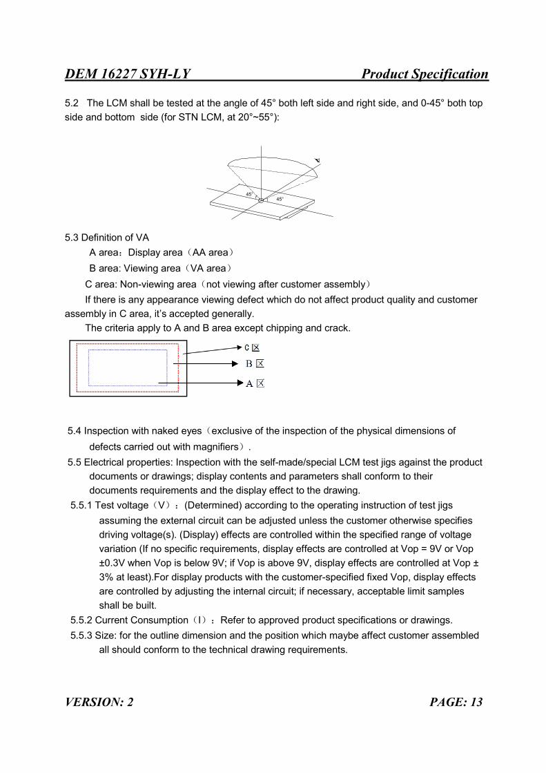
5.2 The LCM shall be tested at the angle of 45° both left side and right side, and 0-45° both top side and bottom side (for STN LCM, at 20°~55°):
5.3 Definition of VA A area:Display area(AA area) B area: Viewing area(VA area)
C area: Non-viewing area(not viewing after customer assembly) If there is any appearance viewing defect which do not affect product quality and customer
assembly in C area, it’s accepted generally. The criteria apply to A and B area except chipping and crack.
5.4 Inspection with naked eyes(exclusive of the inspection of the physical dimensions of
defects carried out with magnifiers). 5.5 Electrical properties: Inspection with the self-made/special LCM test jigs against the product
documents or drawings; display contents and parameters shall conform to their documents requirements and the display effect to the drawing.
5.5.1 Test voltage(V):(Determined) according to the operating instruction of test jigs assuming the external circuit can be adjusted unless the customer otherwise specifies driving voltage(s). (Display) effects are controlled within the specified range of voltage variation (If no specific requirements, display effects are controlled at Vop = 9V or Vop ±0.3V when Vop is below 9V; if Vop is above 9V, display effects are controlled at Vop ± 3% at least).For display products with the customer-specified fixed Vop, display effects are controlled by adjusting the internal circuit; if necessary, acceptable limit samples shall be built.
5.5.2 Current Consumption(I):Refer to approved product specifications or drawings. 5.5.3 Size: for the outline dimension and the position which maybe affect customer assembled
all should conform to the technical drawing requirements.
45°45°
DEM 16227 SYH-LY Product Specification
VERSION: 2 PAGE: 14
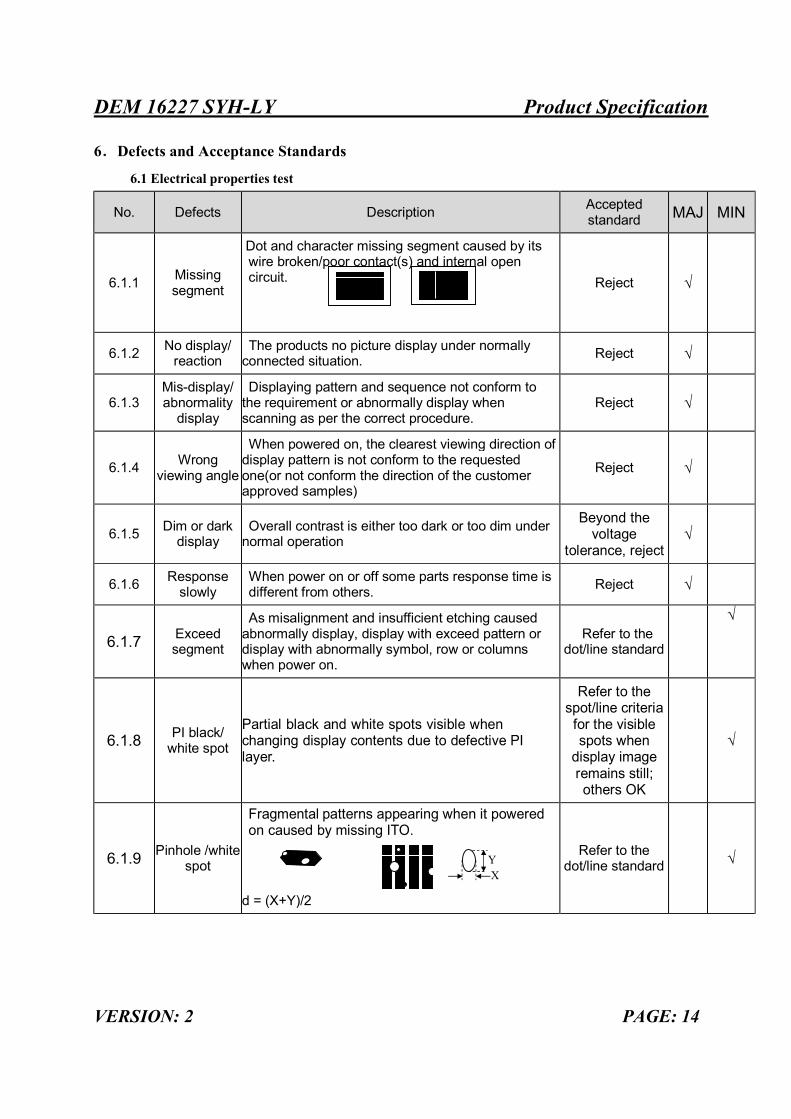
6.Defects and Acceptance Standards
6.1 Electrical properties test
No. Defects Description Accepted standard MAJ MIN
6.1.1 Missing segment
Dot and character missing segment caused by its wire broken/poor contact(s) and internal open circuit.
Reject √
6.1.2 No display/ reaction
The products no picture display under normally connected situation. Reject √
6.1.3 Mis-display/ abnormality
display
Displaying pattern and sequence not conform to the requirement or abnormally display when scanning as per the correct procedure.
Reject √
6.1.4 Wrong viewing angle
When powered on, the clearest viewing direction of display pattern is not conform to the requested one(or not conform the direction of the customer approved samples)
Reject √
6.1.5 Dim or dark display
Overall contrast is either too dark or too dim under normal operation
Beyond the voltage
tolerance, reject √
6.1.6 Response slowly
When power on or off some parts response time is different from others. Reject √
6.1.7 Exceed segment
As misalignment and insufficient etching caused abnormally display, display with exceed pattern or display with abnormally symbol, row or columns when power on.
Refer to the dot/line standard
√
6.1.8 PI black/ white spot
Partial black and white spots visible when changing display contents due to defective PI layer.
Refer to the spot/line criteria
for the visible spots when
display image remains still; others OK
√
6.1.9 Pinhole /white spot
Fragmental patterns appearing when it powered on caused by missing ITO.
d = (X+Y)/2
Refer to the dot/line standard √ Y
X
DEM 16227 SYH-LY Product Specification
VERSION: 2 PAGE: 15
6.1.10 Pattern
distortion
The pattern displayed width is either wider, narrower or deformed than the specified, caused by its misalignment and resulting in unwanted heave(s) or missing:|Ia-Ib|≤1/4W(W is the normal width)
|Ia-Ib|>1/4W,
Reject √
6.1.11 Voltage
When normally working the bias between measured voltage and designed voltage is more than ±4% (if at or below 5V, inspect at the tolerance of +/-0.2V)
Reject √
6.1.12 High current The current of LCD is higher than the standard one. Reject √ 6.2 LCD appearance defect: 6.2.1 Dot and line defects (defined within VA, spots out of VA do not account)
NO. Items Average diameter (d)
Acceptable quantity
MAJ MIN VA≤600mm2
600mm2<VA≤5000mm2
5000mm2 <VA≤20000
mm2
6.2.1.1
Spot defects
(black spot, foreign material, nick, scratches,
including LC with wrong orientation)
d≤0.10 Not counted Not counted Not counted
√
0.10<d≤0.20 3 3 4
0.20<d≤0.25 0 1
0.25<d≤0.30 0 0 1
0.30<d≤0.40 0 0 0
0.40<d 0 0 0
6.2.1.2
Line defects (scratches and linear foreign
materials) Line length=L Line width=W
W≤0.01 Not counted Not counted
Not counted
√
L≤2.0,W≤0.02 2 3
L≤3.0,W≤0.03 1 2 3
L≤3.0,W≤0.05 0 1 2
Note: when W>0.1mm it can regard as spot defect.
6.2.1.3
Polarizer with air bubble or
convex-concave dots defect
W
d≤0.15 Not counted
Not counted Not counted
√ 0.15<d≤0.3 2 3 3
DEM 16227 SYH-LY Product Specification
VERSION: 2 PAGE: 16
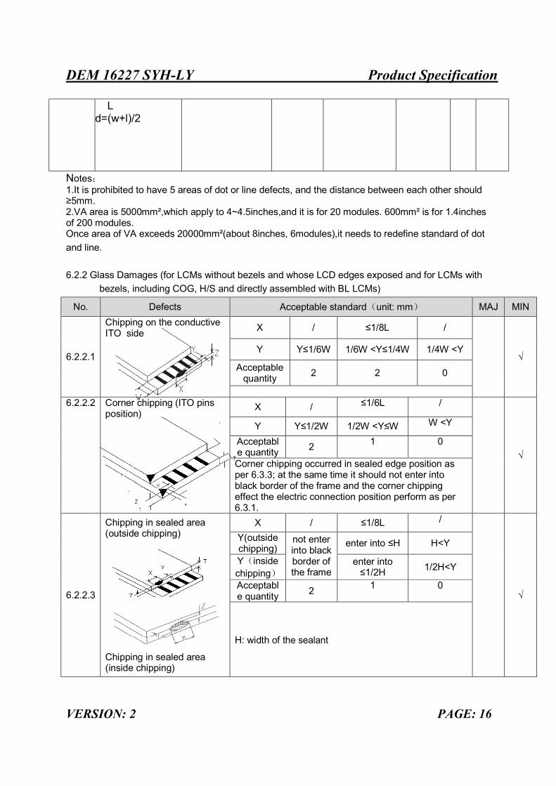
L d=(w+l)/2
Notes: 1.It is prohibited to have 5 areas of dot or line defects, and the distance between each other should ≥5mm. 2.VA area is 5000mm²,which apply to 4~4.5inches,and it is for 20 modules. 600mm² is for 1.4inches of 200 modules. Once area of VA exceeds 20000mm²(about 8inches, 6modules),it needs to redefine standard of dot and line. 6.2.2 Glass Damages (for LCMs without bezels and whose LCD edges exposed and for LCMs with
bezels, including COG, H/S and directly assembled with BL LCMs)
No. Defects Acceptable standard(unit: mm) MAJ MIN
6.2.2.1
Chipping on the conductive ITO side X / ≤1/8L /
√ Y Y≤1/6W 1/6W <Y≤1/4W 1/4W <Y
Acceptable quantity 2 2 0
6.2.2.2 Corner chipping (ITO pins
position)
X / ≤1/6L /
√
Y Y≤1/2W 1/2W <Y≤W W <Y
Acceptable quantity 2 1 0
Corner chipping occurred in sealed edge position as per 6.3.3; at the same time it should not enter into black border of the frame and the corner chipping effect the electric connection position perform as per 6.3.1.
6.2.2.3
Chipping in sealed area (outside chipping)
Chipping in sealed area (inside chipping)
X / ≤1/8L /
√
Y(outside chipping)
not enter into black border of the frame
enter into ≤H H<Y
Y(inside chipping)
enter into ≤1/2H 1/2H<Y
Acceptable quantity 2 1 0
H: width of the sealant
DEM 16227 SYH-LY Product Specification
VERSION: 2 PAGE: 17
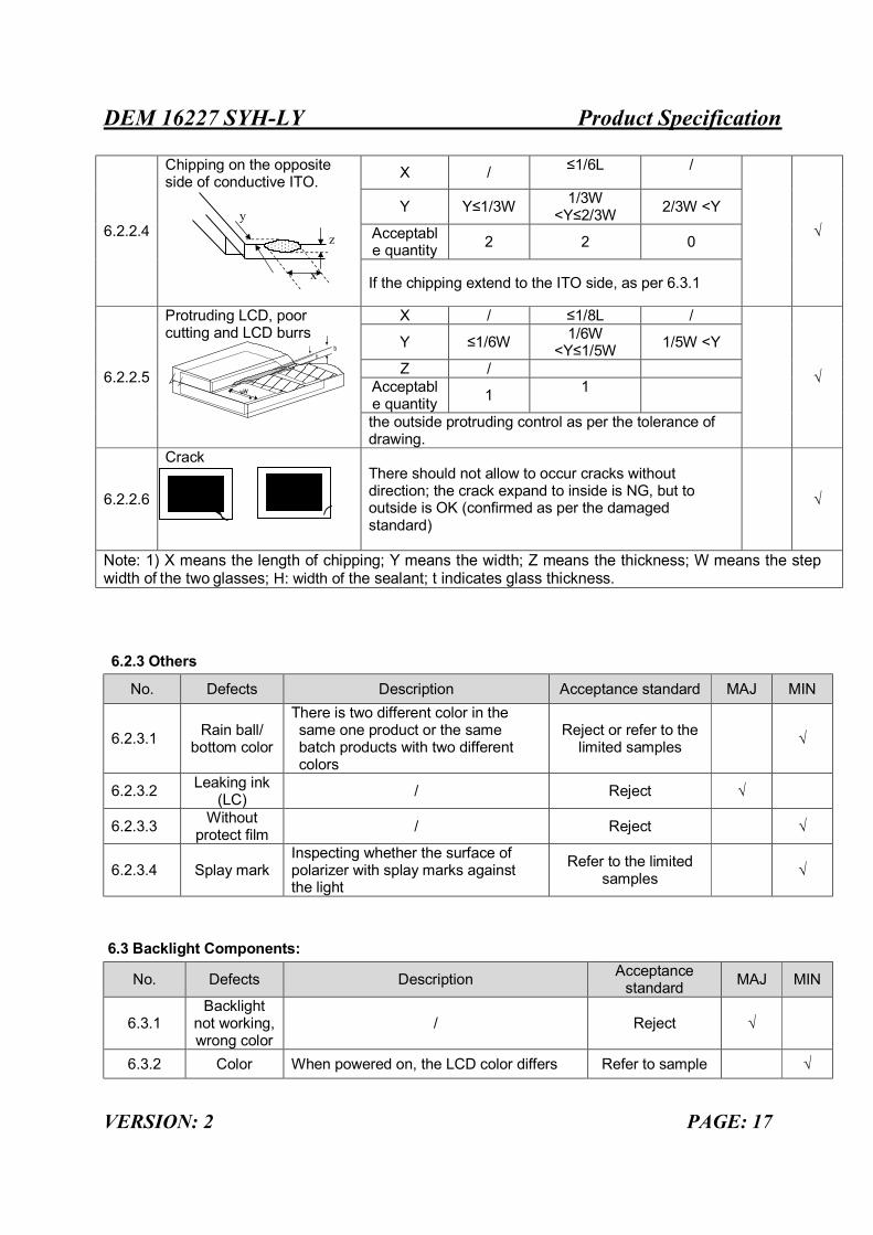
6.2.2.4
Chipping on the opposite side of conductive ITO.
X / ≤1/6L /
√ Y Y≤1/3W 1/3W
<Y≤2/3W 2/3W <Y
Acceptable quantity 2 2 0
If the chipping extend to the ITO side, as per 6.3.1
6.2.2.5
Protruding LCD, poor cutting and LCD burrs
X / ≤1/8L /
√
Y ≤1/6W 1/6W <Y≤1/5W 1/5W <Y
Z / Acceptable quantity 1 1
the outside protruding control as per the tolerance of drawing.
6.2.2.6
Crack
There should not allow to occur cracks without direction; the crack expand to inside is NG, but to outside is OK (confirmed as per the damaged standard)
√
Note: 1) X means the length of chipping; Y means the width; Z means the thickness; W means the step width of the two glasses; H: width of the sealant; t indicates glass thickness.
6.2.3 Others
No. Defects Description Acceptance standard MAJ MIN
6.2.3.1 Rain ball/ bottom color
There is two different color in the same one product or the same batch products with two different colors
Reject or refer to the limited samples √
6.2.3.2 Leaking ink (LC) / Reject √
6.2.3.3 Without protect film / Reject √
6.2.3.4 Splay mark Inspecting whether the surface of polarizer with splay marks against the light
Refer to the limited samples √
6.3 Backlight Components:
No. Defects Description Acceptance standard MAJ MIN
6.3.1 Backlight
not working, wrong color
/ Reject √
6.3.2 Color When powered on, the LCD color differs Refer to sample √
b
w
b
w
x
z
y
DEM 16227 SYH-LY Product Specification
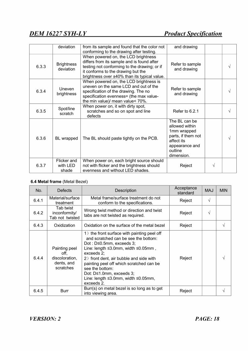
VERSION: 2 PAGE: 18
deviation from its sample and found that the color not conforming to the drawing after testing.
and drawing
6.3.3 Brightness deviation
When powered on, the LCD brightness differs from its sample and is found after testing not conforming to the drawing; or if it conforms to the drawing but the brightness over ±40% than its typical value.
Refer to sample and drawing √
6.3.4 Uneven brightness
When powered on, the LCD brightness is uneven on the same LCD and out of the specification of the drawing. The no specification evenness= (the max value- the min value)/ mean value< 70%.
Refer to sample and drawing √
6.3.5 Spot/line scratch
When power on, it with dirty spot, scratches and so on spot and line defects
Refer to 6.2.1 √
6.3.6 BL wrapped The BL should paste tightly on the PCB.
The BL can be allowed within 1mm wrapped parts, if them not affect its appearance and outline dimension.
√
6.3.7 Flicker and with LED
shade
When power on, each bright source should not with flicker and the brightness should evenness and without LED shades.
Reject √
6.4 Metal frame (Metal Bezel)
No. Defects Description Acceptance standard MAJ MIN
6.4.1 Material/surface treatment
Metal frame/surface treatment do not conform to the specifications. Reject √
6.4.2 Tab twist
inconformity/ Tab not twisted
Wrong twist method or direction and twist tabs are not twisted as required. Reject √
6.4.3 Oxidization Oxidation on the surface of the metal bezel Reject √
6.4.4
Painting peel off,
discoloration, dents, and scratches
1)the front surface with painting peel off and scratched can be see the bottom:
Dot : D≤0.5mm, exceeds 3; Line: length ≤3.0mm, width ≤0.05mm , exceeds 2; 2)front dent, air bubble and side with painting peel off which scratched can be see the bottom: Dot: D≤1.0mm, exceeds 3; Line: length ≤3.0mm, width ≤0.05mm, exceeds 2.
Reject √
6.4.5 Burr Burr(s) on metal bezel is so long as to get into viewing area. Reject √
DEM 16227 SYH-LY Product Specification
VERSION: 2 PAGE: 19
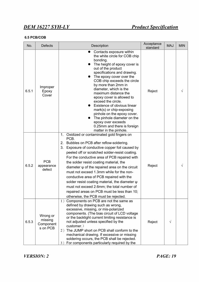
6.5 PCB/COB
No. Defects Description Acceptance standard MAJ MIN
6.5.1 Improper
Epoxy Cover
l Contacts exposure within the white circle for COB chip bonding.
l The height of epoxy cover is out of the product specifications and drawing.
l The epoxy cover over the COB chip exceeds the circle by more than 2mm in diameter, which is the maximum distance the epoxy cover is allowed to exceed the circle.
l Existence of obvious linear mark(s) or chip-exposing pinhole on the epoxy cover.
l The pinhole diameter on the epoxy over exceeds 0.25mm and there is foreign matter in the pinhole.
Reject √
6.5.2 PCB
appearance defect
1. Oxidized or contaminated gold fingers on PCB.
2. Bubbles on PCB after reflow-soldering. 3. Exposure of conductive copper foil caused by
peeled off or scratched solder-resist coating. For the conductive area of PCB repaired with the solder resist coating material, the diameter ψ of the repaired area on the circuit must not exceed 1.3mm while for the non-conductive area of PCB repaired with the solder resist coating material, the diameter ψ must not exceed 2.6mm; the total number of repaired areas on PCB must be less than 10; otherwise, the PCB must be rejected.
Reject √
6.5.3
Wrong or missing
Components on PCB
1) Components on PCB are not the same as defined by drawing such as wrong, excessive, missing, or mis-polarized components. (The bias circuit of LCD voltage or the backlight current limiting resistance is not adjusted unless specified by the customer.)
2) The JUMP short on PCB shall conform to the mechanical drawing. If excessive or missing soldering occurs, the PCB shall be rejected.
3) For components particularly required by the
Reject √
DEM 16227 SYH-LY Product Specification
VERSION: 2 PAGE: 20
customer and specified in the mechanical drawing and/or component specifications, their specifications must conform to those of the suppliers; otherwise they shall be rejected.
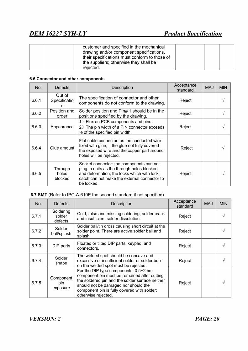
6.6 Connector and other components
No. Defects Description Acceptance standard MAJ MIN
6.6.1 Out of
Specification
The specification of connector and other components do not conform to the drawing. Reject √
6.6.2 Position and order
Solder position and Pin# 1 should be in the positions specified by the drawing. Reject √
6.6.3 Appearance 1)Flux on PCB components and pins. 2)The pin width of a PIN connector exceeds ½ of the specified pin width.
Reject √
6.6.4 Glue amount
Flat cable connector: as the conducted wire fixed with glue, if the glue not fully covered the exposed wire and the copper part around holes will be rejected.
Reject √
6.6.5 Through
holes blocked
Socket connector: the components can not plug-in units as the through holes blocked and deformation; the locks which with lock catch can not make the external connector to be locked.
Reject √
6.7 SMT (Refer to IPC-A-610E the second standard if not specified)
No. Defects Description Acceptance standard MAJ MIN
6.7.1 Soldering
solder defects
Cold, false and missing soldering, solder crack and insufficient solder dissolution. Reject √
6.7.2 Solder ball/splash
Solder ball/tin dross causing short circuit at the solder point. There are active solder ball and splash.
Reject √
6.7.3 DIP parts Floated or tilted DIP parts, keypad, and connectors. Reject √
6.7.4 Solder shape
The welded spot should be concave and excessive or insufficient solder or solder burr on the welded spot must be rejected.
Reject √
6.7.5 Component
pin exposure
For the DIP type components, 0.5~2mm component pin must be remained after cutting the soldered pin and the solder surface neither should not be damaged nor should the component pin is fully covered with solder; otherwise rejected.
Reject √
DEM 16227 SYH-LY Product Specification
VERSION: 2 PAGE: 21
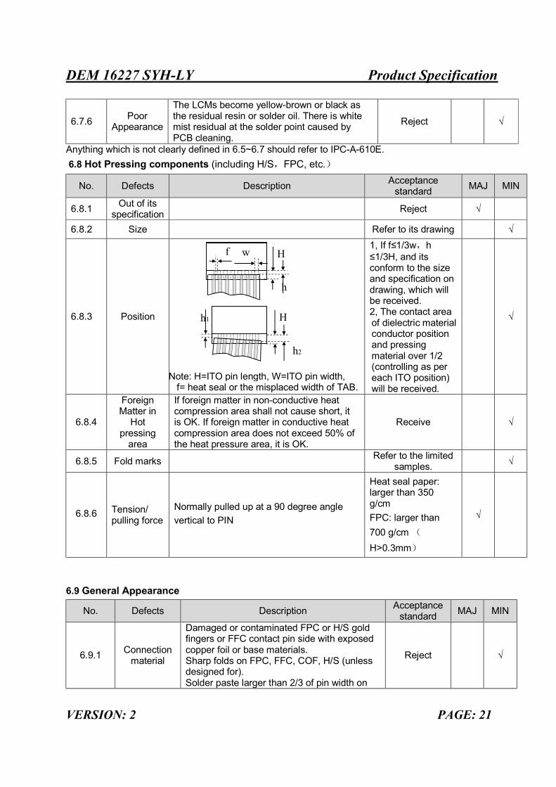
6.7.6 Poor Appearance
The LCMs become yellow-brown or black as the residual resin or solder oil. There is white mist residual at the solder point caused by PCB cleaning.
Reject √
Anything which is not clearly defined in 6.5~6.7 should refer to IPC-A-610E. 6.8 Hot Pressing components (including H/S,FPC, etc.)
No. Defects Description Acceptance standard MAJ MIN
6.8.1 Out of its specification Reject √
6.8.2 Size Refer to its drawing √
6.8.3 Position
Note: H=ITO pin length, W=ITO pin width,
f= heat seal or the misplaced width of TAB.
1, If f≤1/3w,h ≤1/3H, and its conform to the size and specification on drawing, which will be received. 2, The contact area of dielectric material conductor position and pressing material over 1/2 (controlling as per each ITO position) will be received.
√
6.8.4
Foreign Matter in
Hot pressing
area
If foreign matter in non-conductive heat compression area shall not cause short, it is OK. If foreign matter in conductive heat compression area does not exceed 50% of the heat pressure area, it is OK.
Receive √
6.8.5 Fold marks Refer to the limited samples. √
6.8.6 Tension/ pulling force
Normally pulled up at a 90 degree angle vertical to PIN
Heat seal paper: larger than 350 g/cm FPC: larger than 700 g/cm (H>0.3mm)
√
6.9 General Appearance
No. Defects Description Acceptance standard MAJ MIN
6.9.1 Connection material
Damaged or contaminated FPC or H/S gold fingers or FFC contact pin side with exposed copper foil or base materials. Sharp folds on FPC, FFC, COF, H/S (unless designed for). Solder paste larger than 2/3 of pin width on
Reject √
w f H
h
h2
H h1
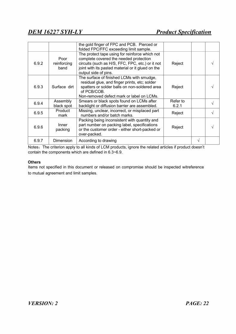
DEM 16227 SYH-LY Product Specification
VERSION: 2 PAGE: 22
the gold finger of FPC and PCB. Pierced or folded FPC/FFC exceeding limit sample.
6.9.2 Poor
reinforcing band
The protect tape using for reinforce which not complete covered the needed protection circuits (such as H/S, FFC, FPC, etc.) or it not joint with its pasted material or it glued on the output side of pins.
Reject √
6.9.3 Surface dirt
The surface of finished LCMs with smudge, residual glue, and finger prints, etc; solder spatters or solder balls on non-soldered area of PCB/COB.
Non-removed defect mark or label on LCMs.
Reject √
6.9.4 Assembly black spot
Smears or black spots found on LCMs after backlight or diffusion barrier are assembled.
Refer to 6.2.1 √
6.9.5 Product mark
Missing, unclear, incorrect, or misplaced part numbers and/or batch marks. Reject √
6.9.6 Inner packing
Packing being inconsistent with quantity and part number on packing label, specifications or the customer order - either short-packed or over-packed.
Reject √
6.9.7 Dimension According to drawing √ Notes:The criterion apply to all kinds of LCM products, ignore the related articles if product doesn’t contain the components which are defined in 6.3~6.9. Others Items not specified in this document or released on compromise should be inspected witreference to mutual agreement and limit samples.
DEM 16227 SYH-LY Product Specification
VERSION: 2 PAGE: 23
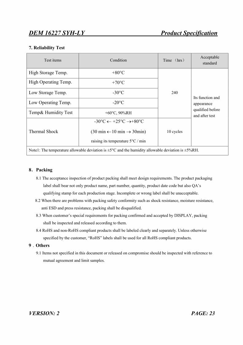
7. Reliability Test
Test items Condition Time (hrs) Acceptable
standard
High Storage Temp. +80°C
240 Its function and appearance qualified before and after test
High Operating Temp. +70°C
Low Storage Temp. -30°C
Low Operating Temp. -20°C
Temp& Humidity Test +60°C, 90%RH
Thermal Shock
-30°C ← +25°C →+80°C
(30 min ←10 min → 30min)
raising its temperature 5°C / min
10 cycles
Note1: The temperature allowable deviation is ±5°C and the humidity allowable deviation is ±5%RH.
8.Packing
8.1 The acceptance inspection of product packing shall meet design requirements. The product packaging
label shall bear not only product name, part number, quantity, product date code but also QA’s
qualifying stamp for each production stage. Incomplete or wrong label shall be unacceptable.
8.2 When there are problems with packing safety conformity such as shock resistance, moisture resistance,
anti ESD and press resistance, packing shall be disqualified.
8.3 When customer’s special requirements for packing confirmed and accepted by DISPLAY, packing
shall be inspected and released according to them.
8.4 RoHS and non-RoHS compliant products shall be labeled clearly and separately. Unless otherwise
specified by the customer, “RoHS” labels shall be used for all RoHS compliant products.
9.Others
9.1 Items not specified in this document or released on compromise should be inspected with reference to
mutual agreement and limit samples.
Related Documents


![TME-DC [ ] - Sew Many Parts, Inc. of Contents z TME-DC GENERAL VIEW z TME-DC FRAME … CD-1 z TME-DC TABLE … CD-2-1 z TME-DC AUTO SUB TABLE …](https://static.cupdf.com/doc/110x72/5b1d28797f8b9add7f8b64eb/tme-dc-sew-many-parts-inc-of-contents-z-tme-dc-general-view-z-tme-dc-frame.jpg)


