Welcome message from author
This document is posted to help you gain knowledge. Please leave a comment to let me know what you think about it! Share it to your friends and learn new things together.
Transcript


Delhi - 1100922009
DIGITAL LOGIC ANDCOMPUTER ORGANIZATION
V. RAJARAMANHonorary Professor
Supercomputer Education and Research CentreIndian Institute of Science, Bangalore
T. RADHAKRISHNANProfessor of Computer Science and Software Engineering
Concordia UniversityMontreal, Canada

DIGITAL LOGIC AND COMPUTER ORGANIZATIONV. Rajaraman and T. Radhakrishnan
© 2006 by PHI Learning Private Limited, Delhi. All rights reserved. No part of this book may bereproduced in any form, by mimeograph or any other means, without permission in writing fromthe publisher.
ISBN-978-81-203-2979-9
The export rights of this book are vested solely with the publisher.
Third Printing … … … April, 2009
Published by Asoke K. Ghosh, PHI Learning Private Limited, Rimjhim House, 111 PatparganjIndustrial Estate, Delhi-110092 and Printed by Rajkamal Electric Press, B-35/9, G.T. Karnal RoadIndustrial Area, Delhi-110033.
iii
Preface xi
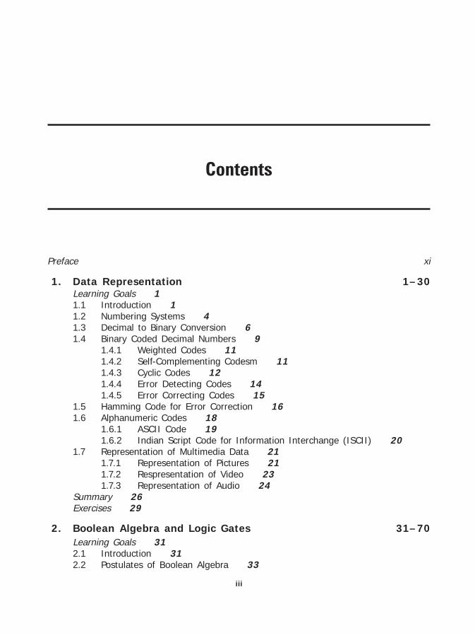
1. Data Representation 1–30Learning Goals 11.1 Introduction 11.2 Numbering Systems 41.3 Decimal to Binary Conversion 61.4 Binary Coded Decimal Numbers 9
1.4.1 Weighted Codes 111.4.2 Self-Complementing Codesm 111.4.3 Cyclic Codes 121.4.4 Error Detecting Codes 141.4.5 Error Correcting Codes 15
1.5 Hamming Code for Error Correction 161.6 Alphanumeric Codes 18
1.6.1 ASCII Code 191.6.2 Indian Script Code for Information Interchange (ISCII) 20
1.7 Representation of Multimedia Data 211.7.1 Representation of Pictures 211.7.2 Respresentation of Video 231.7.3 Representation of Audio 24
Summary 26Exercises 29
2. Boolean Algebra and Logic Gates 31–70Learning Goals 312.1 Introduction 312.2 Postulates of Boolean Algebra 33
Contents

iv Contents
2.3 Basic Theorems of Boolean Algebra 342.3.1 Duality Principle 352.3.2 Theorems 352.3.3 Precedence of Operators 372.3.4 Venn Diagram 37
2.4 Boolean Functions and Truth Tables 392.5 Canonical Forms for Boolean Functions 402.6 Binary Operators and Logic Gates 442.7 Simplifying Boolean Expressions 492.8 Veitch-Karnaugh Map Method 52
2.8.1 Four Variable Karnaugh Map 562.8.2 Incompletely Specified Function 59
2.9 Quine-McCluskey Procedure 602.10 Conclusions 67Summary 68Exercises 69
3. Combinatorial Switching Circuits 71–128Learning Goals 713.1 Introduction 713.2 Combinatorial Circuit Design Procedure 723.3 Integrated NAND-NOR Gates 81
3.3.1 CMOS Transistor Gates 823.3.2 NAND-NOR Gates with CMOS Transistors 85
3.4 Open Drain and Tri-state Gates 923.4.1 Wired AND Gate 943.4.2 Driving a Bus from Many Sources 953.4.3 Tri-state Gates 95
3.5 Realization of Boolean Expressions Using NAND/NOR Gates 973.6 Combinatorial Circuits Commonly Used in Digital Systems 1013.7 Design of Combinatorial Circuits with Multiplexers 1083.8 Programmable Logic Devices 117
3.8.1 Realization with FPLAs 1183.8.2 Realization with PALs 121
Summary 125Exercises 126
4. Sequential Switching Circuits 129 –188Learning Goals 1294.1 Introduction 1294.2 A Basic Sequential Circuit 1324.3 Types of Sequential Circuits 1344.4 Flip-Flops 1374.5 Counters 147
4.5.1 A Binary Counter 1474.5.2 Synchronous Binary Counter 148

Contents v
4.6 Modelling Sequential Circuits—Finite State Machines 1504.7 Synthesis of Synchronous Binary Counters 153
4.7.1 Modulo-5 Counter 1534.7.2 Modulo-10 Counter 1564.7.3 Generation of Control Signals 1584.7.4 Controlled Counter 160
4.8 Synthesizing General Sequential Circuits 1624.8.1 Synthesizing a Moore Machine 1624.8.2 Synthesizing a Mealy Machine 163
4.9 Shift Registers 1644.10 Modelling, Analysis and Design of Sequential Circuits 1684.11 Implementation of Sequential Circuits with MSIs 180Summary 185Exercises 187
5. Arithmetic and Logic Unit 189 –240Learning Goals 1895.1 Introduction 1895.2 Binary Addition 1905.3 Binary Subtraction 1915.4 Complement Representation of Numbers 1945.5 Addition/Subtraction of Numbers in 1’s Complement Notation 1955.6 Addition/Subtraction of Numbers in Two’s Complement Notation 1975.7 Binary Multiplication 1995.8 Multiplication of Signed Numbers 2025.9 Binary Division 2065.10 Integer Representation 2105.11 Floating Point Representation of Numbers 210
5.11.1 Binary Floating Point Numbers 2135.11.2 IEEE Standard Floating Point Representation 216
5.12 Floating Point Addition/Subtraction 2215.12.1 Floating Point Multiplication 2235.12.2 Floating Point Division 223
5.13 Floating Point Arithmetic Operations 2245.14 Logic Circuits for Addition/Subtraction 226
5.14.1 Half- and Full-Adder Using Gates 2265.14.2 A Four-bit Adder 2295.14.3 MSI Arithmetic Logic Unit 232
5.15 A Combinatorial Circuit for Multiplication 235Summary 237Exercises 239
6. Application of Sequential Circuits 241–263Learning Goals 2416.1 Introduction 2416.2 Algorithmic State Machine 242

vi Contents
6.3 Algorithmic Representation of ASM Charts 2496.4 Designing Digital Systems Using ASM Chart 2526.5 Floating Point Adder 258Summary 261Exercises 262
7. Computer Systems—Multiple Views 264 –276Learning Goals 2647.1 Introduction 2647.2 A Layered View of a Computer System 265
7.2.1 Hardware Level 2667.2.2 Machine and Assembly Language Levels 2677.2.3 Higher Level Language 2687.2.4 Operating System Level 2697.2.5 Application Level: Loading a Machine Language Program 270
7.3 Performance Measures 273Summary 274Exercises 275
8. Basic Computer Organization 277–316Learning Goals 2778.1 Introduction 2778.2 Memory Organization of SMAC (S1) 2788.3 Instruction and Data Representation 2798.4 CPU Organization 2818.5 Input/Output for SMAC 2828.6 Programming SMAC with Instruction Set S1 2828.7 Instruction Set S2 and SMAC+ 2848.8 Organization of SMAC+ 2878.9 Assembling the Program into Machine Language Format 2938.10 Simulation of SMAC+ 2948.11 Program Execution and Tracing 2968.12 Expanding the Instruction Set Further 2988.13 Vector Operations and Indexing 3008.14 Stacks 3028.15 Modular Organization and Developing Large Programs 3058.16 Enhanced Architecture—SMAC++ 310
8.16.1 Modifications in the Instruction Formats for SMAC++ 3128.17 Conclusions 313Summary 314Exercises 314
9. Central Processing Unit 317–349Learning Goals 3179.1 Introduction 3179.2 Operation Code Encoding and Decoding 319

Contents vii
9.3 Instruction Set and Instruction Formats 3229.3.1 Instruction Set 3229.3.2 Instruction Format 324
9.4 Addressing Modes 3279.4.1 Base Addressing 3289.4.2 Segment Addressing 3299.4.3 PC Relative Addressing 3309.4.4 Indirect Addressing 3309.4.5 How to Encode Various Addressing Modes 331
9.5 Register Sets 3329.6 Clocks and Timing 3349.7 CPU Buses 3369.8 Dataflow, Data Paths and Microprogramming 3399.9 Control Flow 3449.10 Summary of CPU Organization 347Summary 348Exercises 348
10. Memory Organization 350 –399Learning Goals 35010.1 Introduction 35010.2 Memory Parameters 35110.3 Semiconductor Memory Cell 353
10.3.1 Dynamic Memory Cell 35310.3.2 Static Memory Cell 35410.3.3 Writing Data in Memory Cell 35510.3.4 Reading the Contents of Cell 356
10.4 IC Chips for Organization of RAMs 35710.5 2D Organization of Semiconductor Memory 35810.6 2.5D Organization of Memory Systems 36010.7 Dynamic Random Access Memory 36310.8 Error Detection and Correction in Memories 36610.9 Read Only Memory 36610.10 Dual-Ported RAM 36910.11 Enhancing Speed and Capacity of Memories 37010.12 Program Behaviour and Locality Principle 37110.13 A Two-Level Hierarchy of Memories 37410.14 Cache in Memory Organization 37610.15 Design and Performance of Cache Memory System 38510.16 Virtual Memory—Another Level in Hierarchy 387
10.16.1 Address Translation 38810.16.2 Page Replacement 39010.16.3 Page Fetching 39310.16.4 Page Size 393

viii Contents
10.16.5 How to Make Address Translation Faster 39410.16.6 Page Table Size 395
Summary 396Exercises 398
11. Input-Output Devices 400–433Learning Goals 40011.1 Introduction 40011.2 Video Display Terminal Characteristics 40111.3 Cathode Ray Tube Display 402
11.3.1 Colour Display Tube 40411.4 Raster-Scan Display Device 40511.5 Raster-Scan Display Processing Unit 40611.6 Flat Panel Display 408
11.6.1 Principles of Operation of Liquid Crystal Displays 40911.7 Input Devices 41011.8 Hard Copy Output Units 412
11.8.1 Inkjet Printer 41311.8.2 Laser Printers 41411.8.3 Line Printers 414
11.9 Hard Disk Drives 41511.9.1 Redundant Array of Inexpensive Disks (RAID) 420
11.10 Floppy Disk Drives 42211.11 Compact Disk Read Only Memory (CDROM) 422
11.11.1 Digital Versatile Disk Read Only Memory (DVD-ROM) 42411.11.2 CD-R (Recordable CD-ROM or Write Once CD-ROM—WOROM) 425
11.12 Magnetic Tape Drives 42511.12.1 Ultrium Cartridge Tape Drive 42511.12.2 Digital Audio Tapes (DAT) 426
Summary 427Exercises 430
12. Input-Output Organization 434–479Learning Goals 43412.1 Introduction 43412.2 Device Interfacing 43612.3 Overview of I/O Methods 43812.4 Program Controlled Data Transfer 44012.5 Interrupt Structures 442
12.5.1 Single Levesl Interrupt Processing 44312.5.2 Handling Multiple Interrupts 445
12.6 Interrupt Controlled Data Transfer 44612.6.1 Software Polling 44612.6.2 Bus Arbitration 44712.6.3 Daisy Chaining 44712.6.4 Vectored Interrupts 448

Contents ix
12.6.5 Multiple Interrupt Lines 44912.6.6 VLSI Chip Interrupt Controller 45012.6.7 Programmable Peripheral Interface Unit 451
12.7 DMA Based Data Transfer 45212.8 Input/Output (I/O) Processors 45712.9 Bus Structure 458
12.9.1 Structure of a Bus 45812.9.2 Types of Bus 45912.9.3 Bus Transaction Type 45912.9.4 Timings of Bus Transactions 45912.9.5 Bus Arbitration 462
12.10 Some Standard Buses 46312.11 Serial Data Communication 466
12.11.1 Asynchronous Serial Data Communication 46612.11.2 Asynchronous Communication Interface Adapter (ACIA) 46712.11.3 Digital Modems 468
12.12 Local Area Networks 46912.12.1 Ethernet Local Area Network—Bus Topology 47012.12.2 Ethernet Using Star Topology 47312.12.3 Wireless LAN 47412.12.4 Client-Server Computing Using LAN 475
Summary 476Exercises 478
13. Case Study of a Real Computer System 480–496Learning Goals 48013.1 Introduction 48013.2 Viewing Pentium as a Member of a Family of Computers 48113.3 Memory System View 48213.4 The Programmer’s View of Pentium Processor 484
13.4.1 General Registers: EAX, EBX, ECX, EDX 48613.4.2 Pointers and Index Registers: ESP, EBP, ESI, EDI 48713.4.3 Segment Registers: CS, DS, SS, ES, FS, GS 48713.4.4 Program Flow Control Registers: EIP and EFLAGS 487
13.5 Instruction Format 48813.6 Instruction Set View 490
13.6.1 Classes of Instructions 49013.7 Interconnecting the Components into a Computer System 493Summary 496Exercises 496
Appendix A Suggested Hardware Lab Experiments 497–502Appendix B Decision Table Terminology 503–504References 505–506Index 507–513

Digital Logic And Computer Organization
Publisher : PHI Learning ISBN : 9788120329799 Author : RAJARAMAN,V., T. RADHAKRISHNAN
Type the URL : http://www.kopykitab.com/product/7409
Get this eBook
25%OFF
Related Documents