Clemson University TigerPrints All Dissertations Dissertations 12-2016 Defects in Graphene: Electrochemical, Magnetic, and Optical Properties Jingyi Zhu Clemson University, [email protected] Follow this and additional works at: hps://tigerprints.clemson.edu/all_dissertations is Dissertation is brought to you for free and open access by the Dissertations at TigerPrints. It has been accepted for inclusion in All Dissertations by an authorized administrator of TigerPrints. For more information, please contact [email protected]. Recommended Citation Zhu, Jingyi, "Defects in Graphene: Electrochemical, Magnetic, and Optical Properties" (2016). All Dissertations. 1809. hps://tigerprints.clemson.edu/all_dissertations/1809

Welcome message from author
This document is posted to help you gain knowledge. Please leave a comment to let me know what you think about it! Share it to your friends and learn new things together.
Transcript

Clemson UniversityTigerPrints
All Dissertations Dissertations
12-2016
Defects in Graphene: Electrochemical, Magnetic,and Optical PropertiesJingyi ZhuClemson University, [email protected]
Follow this and additional works at: https://tigerprints.clemson.edu/all_dissertations
This Dissertation is brought to you for free and open access by the Dissertations at TigerPrints. It has been accepted for inclusion in All Dissertations byan authorized administrator of TigerPrints. For more information, please contact [email protected].
Recommended CitationZhu, Jingyi, "Defects in Graphene: Electrochemical, Magnetic, and Optical Properties" (2016). All Dissertations. 1809.https://tigerprints.clemson.edu/all_dissertations/1809

i
DEFECTS IN GRAPHENE: ELECTROCHEMICAL, MAGNETIC, AND OPTICAL PROPERTIES
______________________________________________________
A Dissertation Presented to
the Graduate School of Clemson University
______________________________________________________
In Partial Fulfillment of the Requirements for the Degree
Doctor of Philosophy Physics
______________________________________________________
by Jingyi Zhu
December 2016 ______________________________________________________
Accepted by:
Dr. Apparao M. Rao, Committee Chair Dr. Jian He
Dr. Shiou-Jyh Hwu Dr. Mark E. Roberts

ii
ABSTRACT
Graphene has attracted tremendous attention due to its unique properties, such as
its two-dimensional structure, zero-band-gap, and linear dispersion relation of its electronic
band structure, which are all very interesting from a fundamental standpoint. In addition,
its ultra-light weight, high surface area, exceptional electrical and thermal conductivities,
as well as robust mechanical strength portends huge potential in diverse applications.
Defects in the otherwise perfectly hexagonal lattice of graphene lead to lattice symmetry
breaking, and the emergence of new fundamental properties of graphene. Therefore, to
understand the role of defects in graphene and further to control the fundamental
characteristics of graphene through quantity and configuration of defects (or defect-
engineering), it is essential to develop effective synthesis methods. This thesis describes
such synthesis methods and the role of controlled defects on the electrochemical, magnetic,
as well as the optical properties of graphene.
Following the first two introductory Chapters, in Chapter 3 I describe the effects of
vacancies and dopants on the electrochemical properties of graphene. Carbon is an
excellent electrode material in high-energy and high-power density supercapacitors (SCs)
due to its economic viability, high-surface area, and high stability. Although graphene has
high theoretical surface area, and hence high double layer capacitance, the net amount of
energy stored in graphene-SCs is much below the theoretical limits due to two inherent
bottlenecks: i) their low quantum capacitance, and ii) limited ion-accessible surface area.
We demonstrate that properly designed defects in graphene effectively mitigates these

iii
bottlenecks by drastically increasing the quantum capacitance and opening new channels
to facilitate ion diffusion in the otherwise inaccessible interlayer gallery space in few layer
graphene. Our results support the emergence of a new energy paradigm in SCs with 150%
enhancement in double layer capacitance beyond the theoretical limit. Furthermore, we
demonstrate defect engineering in graphene foams as an example of prototype bulk SCs
with energy densities of 500% higher than the state-of-the-art commercial SCs without
compromising the power density.
Chapter 4 focuses on the magnetic properties of graphene when a dopant, such as a
sulfur atom, is incorporated into the hexagonal framework of graphene. Bulk graphite is
diamagnetic in nature, however, graphene is known to exhibit either a paramagnetic
response or weak ferromagnetic ordering. Although many groups have attributed this
magnetism in graphene to defects or presence of unintentional magnetic impurities,
compelling evidence to pinpoint origin of magnetism in graphene was lacking. To address
this issue, we systematically studied the influence of entropically necessary intrinsic
defects (e.g., vacancies, edges) and extrinsic dopants (e.g., S-dopants) on the magnetic
properties of graphene. We found that the saturation magnetization of graphene decreased
upon sulfur doping suggesting that S-dopants demagnetized vacancies and edges. Our
density functional theory calculations provided evidence for: i) intrinsic defect
demagnetization by the formation of covalent bonds between S-dopant and
edges/vacancies concurring with the experimental results, and ii) a net magnetization from
only zig-zag edges, suggesting that the contradictory conclusions on graphene magnetism
reported in the literature may stem from the magnetic properties due to different defect-

iv
types. Interestingly, we observed peculiar local maxima in the temperature dependent
magnetizations that suggest the coexistence of different magnetic phases within the same
graphene samples.
Finally, in Chapter 5, we demonstrated the relation between defects in graphene
and a Raman feature – the so-called G* band which is present at 2450 cm-1. Although most
of the prominent Raman features in graphene are well understood within the double
resonance (DR) picture, the origin of the G* band still remains unclear. We performed
detailed Raman studies of mechanically exfoliated and chemical vapor deposited single-
and few-layer graphene using multiple laser excitations to unravel the origin of G* band.
Our study concludes that the G* band arises from a combination of transverse optical (iTO)
and longitudinal acoustic (LA) phonons, and its asymmetric lineshape is due to the presence
of two different time-order phonon processes. As detailed in Chapter 5, we attribute the
lower (/higher) frequency sub-peak to an LA-first (/iTO-first) process. Such time-ordered
processes are necessary to rationalize the dispersion of the G* band sub-peak frequencies
with respect to the excitation energy. Our study also shows that defects in graphene induce
new scattering channels and thereby weaken both the time-ordered combination modes.
Finally, we also discuss that the effect of layer stacking on the structure of the G* band and
attribute its increasing asymmetry to multiple processes between electronic sub-bands,
similar to the physics that is responsible for the G’ band in multi-layer graphene.

v
DEDICATION
I dedicate my work to the memories of my dearest mom, Wenfeng Zhu, for bringing me to
the world, for the moral, intellectual and physical education she has given me, for her
unconditional love, support, and all the things she has done for me throughout my life.
I dedicate this work to my beloved father, Xisheng Dai, without whose encouragement and
support none of my success would be possible.
I also dedicate this work to my fiancé, Min Zhang and his family for their understanding
and accompanying during all my difficult times. I would like to take this opportunity to
extend my sincere gratitude towards all my family and friends for their help and guidance.

vi
ACKNOWLEDGEMENTS
I would like to express my sincere appreciation to my advisor, Dr. Apparao M. Rao,
for providing me the great opportunity of working in his research group. His inspiration,
guidance and encouragement has motivated me to overcome all the obstacles and
accomplish my goal in these years. It would be impossible to complete this thesis without
the insights and motivations from Dr. Ramakrishna Podila. I cannot count that how many
discussions we’ve had for designing the experiments, analyzing the results and editing the
manuscripts. I thank Dr. Jian He and Dr, Rahul Rao, for their valuable guidance and input
on the magnetic and the Raman spectroscopy projects. Thanks for Dr. Malcolm Skove for
his suggestions on my research, oral presentations and English writing. Also, I would like
to thank the group of Dr. Mark Roberts for their help and collaboration on the
electrochemistry porjects. I express my gratitude to the group of Dr. Anurag Srivastava
(ABV-Indian Institute of Information Technology and Management), the group of Dr. John
Wilkins (Ohio State University), the group of Dr. Anvar Zakhidov (The University of
Texas at Dallas), Dr. Paola Ayala, and Dr. Ye Lin for their collaborations on theoretical
calculations and sample measurements. Many thanks to my dissertation committee
members Dr. Shiou-Jyh Hwu, Dr. Jian He, and Dr. Mark Roberts.
I would not have completed this dissertation without the support of my colleagues:
Drs. Mehmet Karakaya, Deepika Saini and Sriparna Bhattacharya for their introduction
and help of the equipments, techniques and material synthesis, Anthony Childress for his
important help of sample preparation, and all my present and past lab mates at Clemson

vii
Nanomaterials Institute (Herbert Behlow, Lakshman Ventrapragada, Yongchang Dong,
Sai Mallineni, Fengjiao Liu, Achyut Raghavendra, Wren Gregory, Bishwambhar
Senguptafor, Longyu Hu, Xueying Ge, Prakash Parajuli and Joseph Denison) for their
encouragement and support.
I have to appreciate my aunts – Qingqiu Dai and Wennan Zhu, my uncle –
Jingsheng Dai, my cousins – Hui Jin, Xing Jin, Zhenhao Hou, Xiaofeng Chen, Zhengyue
Dai and their families. My gratitude to them for taking great care of my parents, for being
always treating me as their child or sister, for their endless help and encouragements. I am
always feeling be loved and getting spiritual support from all of you.
Finally, I would like to thank all my friends in China and US. Thank to my best
friend Dr. Xueyan He for her encouragement during my PhD life. Particularly, thanks to
my roommate Yamin Liu and her parents, Song and Milan, Tianhong, Yang Gao, Lin Li
and Dan Du, Tianwei and Shasha, Menghan and Yufei, Zhe Zhang, Lin Wang, Xiaoyu
(Bella), Fanchen, Yamei and Chuanchang for making my life in Clemson memorable.

viii
TABLE OF CONTENTS
Page
TITLE PAGE ....................................................................................................................... I
ABSTRACT ....................................................................................................................... II
DEDICATION .................................................................................................................... V
ACKNOWLEDGEMENTS .............................................................................................. VI
TABLE OF CONTENTS ............................................................................................... VIII
LIST OF TABLES ............................................................................................................ XI
LIST OF FIGURES ......................................................................................................... XII
CHAPTER
1. DEFECTS IN GRAPHENE .................................................................................. 1
1.1. Introduction to graphene ................................................................................ 2 1.1.1. Structure of graphene .......................................................................... 2 1.1.2. Defects of graphene ............................................................................. 6
1.2. Synthesis of graphene .................................................................................... 7 1.3. The use of graphene in energy storage devices ............................................. 9
1.3.1. Supercapacitors ................................................................................... 9 1.3.2. Graphene as an ideal electrode material ............................................ 12 1.3.3. Limitation of graphene in application of energy storage devices ..... 13
2. CHARACTERIZATION TECHNIQUES ........................................................... 21
2.1. Electrochemistry Characterization .............................................................. 21 2.1.1. Potentiostat and electrochemistry cell setup ..................................... 21 2.1.2. Cyclic Voltammetry .......................................................................... 24 2.1.3. Charge-discharge ............................................................................... 28 2.1.4. Electrochemical impedance spectroscopy ......................................... 32
2.2. Raman Spectroscopy ................................................................................... 38 2.2.1. Introduction of Raman ...................................................................... 38 2.2.2. Phonon dispersion in graphene ......................................................... 41 2.2.3. Double-resonance process in graphene ............................................. 44

ix
Table of Contents (Continued)
Page
3. ROLE OF DEFECTS AND DOPANTS ON THE ELECTROCHEMICAL PROPERTIES OF GRAPHENE ......................................................................... 48
3.1. Introduction ................................................................................................. 48 3.2. Experiment and Calculation Methods ......................................................... 50
3.2.1. Calculation methods .......................................................................... 50 3.2.2. Synthesis of N-doped few-layer graphene and graphene foam ......... 50 3.2.3. Structural and electrochemical characterizations .............................. 53
3.3. Effects of ion etching induced defects and type of electrolytes on electrochemical properties of graphene ......................................................... 54
3.3.1. Identification of best-suited electrolyte ............................................. 54 3.3.2. Experimental validation of ion-pore size resonance effects .............. 57
3.4. Effects of N-doping on electrochemical properties of graphene ................. 60 3.4.1. N-doping for improved power and energy density ........................... 60 3.4.2. Characterization of N-doped FLG structures .................................... 63 3.4.3. Electrochemical characterization of N-doped FLG .......................... 68
3.5. Realization of high energy and power densities SC devices with defect-engineered graphene electrode ...................................................................... 72
3.6. Conclusions ................................................................................................. 76
4. ROLE OF DEFECTS AND DOPANTS ON THE MAGNETIC PROPERTIES OF S-DOPED GRAPHENE ................................................................................ 78
4.1. Introduction ................................................................................................. 78 4.2. Experiment and calculation methods ........................................................... 80
4.2.1. Synthesis of S-doped graphene ......................................................... 80 4.2.2. Charcterization of structure and magnetic properties ....................... 83 4.2.3. Calculation methods .......................................................................... 84
4.3. Magnetic properties of pristine and S-doped graphene nanoplatelets ......... 85 4.4. Spin-polarized DFT calculations ................................................................. 93 4.5. Conclusions ............................................................................................... 101

x
Table of Contents (Continued)
Page
5. ROLE OF DEFECTS AND DOPANTS ON THE RAMAN SPECTROSCOPY OF GRAPHENE ................................................................................................ 102
5.1. Introduction ............................................................................................... 102 5.2. Experiments and Characterization Methods .............................................. 106 5.3. G*-band of graphene and the time-ordered scattering process ................. 108 5.4. Dependence of G*-bands on defects and temperature .............................. 117 5.5. Conclusions ............................................................................................... 125
6. SUMMARY AND FUTURE WORK ............................................................... 126
APPENDIX ......................................................................................................................128
REFERENCES ................................................................................................................130

xi
LIST OF TABLES
Table Page
4.2.1 Elemental composition of grade M GnPs. Source: XG Sciences materials safety data sheet. ............................................................................... 81
4.3.1 The value of saturated magnetization MS, remnant magnetization Mr and coercivity Hc for pristine, 1.5 wt.% and 3.0 wt.% S doped GnPs under 5 K and 300 K obtained from hysteresis loops. The non-monotonic variation of MS could result from sample-to-sample variations, and does not affect our conclusion that S-dopants demagnetized GnP samples. ............................................................... 87
4.3.2 ICP-MS analysis of pristine and doped graphene showed only ppb levels of Fe contained in all samples ruling out Fe impurities as a possible cause for the observed magnetic response. ................................. 88

xii
LIST OF FIGURES
Figure Page
1.1.1 (a) Bulk graphite is composed of Van der Waals bonded graphene layers, and the black dots within each layer represent the carbon atoms. (b) The honeycomb lattice of graphene. The grey and black colored dots represent the two inequivalent sublattices in the honeycomb lattice. The two unit vectors of graphene are represnted by the dash arrows. The top and bottom egdes represent the armchair edges (green), while the edges on the sides (red) represent the zigzag edges. ......................................................... 3
1.1.2 a) The first Brillouin zone of graphene. b) The electronic dispersion for graphene in the first Brillouin zone. [2] ...................................... 5
1.3.1 The schematic illustration of (a) conventional parallel plate capacitor, (b) the charging/discharging process in a supercapacitor. ................................................................................................. 10
1.3.2 A Ragone plot of the specific energy and specific power densities of energy storage devices. The overarching goal is increase both the energy density and power density of any of the storage device to match that of gasoline. [20] ......................................................................... 11
1.3.3 a) A schematic of a 2D transistor. b) A positive VG causes the conduction band minimum to be lowered by eVG. ........................................... 14
1.3.4 a) The expected and the actual dependence of the area charge density in the channel as a function of gate voltage. b) Schematic of the circuit that has quantum capacitance and the electrostatic capacitance connected in series. c) In EDLC the quantum capacitance and the double layer capacitance are connected in series. ................................................................................................................ 16
2.1.1 a) A picture of Gamry Reference 3000AE potentiostat. b) Simplified schematic of a potentiostat. (Figure source: Gamry instruments website) ........................................................................................ 22
2.1.2 Schematics for a) two-electrode cell setup, b) three-electrode cell setup. ................................................................................................................ 23

xiii
List of Figures (Continued)
Figure Page
2.1.3 a) Three cycles of the time dependent applied voltage in a typical cyclic voltammetry study. The voltage is scanned in range of 0 – 1.2 V with a scan rate of 100 mV/s. b) A cyclic voltammogram is the plot of the response current at the working electrode to the applied excitation potential. A cyclic voltammogram over one charge-discharge cycle of a 6 F commercial electric double layer capacitor is shown. ........................................................................................... 25
2.1.4 a) A cyclic voltammogram of 10 mM K3Fe(CN)6 at a Pt working electrode in aqueous 0.1 M NaCl solution. b) Schematics of the reduction/oxidation process of species from electrolyte during CV. (Figure from Ref. [28]) ............................................................................. 27
2.1.5 Charge-discharge curve of an EDLC device with two symmetric electrodes made of multiwall carbon nanotubes in 1 M HClO4 aqueous electrolyte. Current density: 50 A/g. .................................................. 29
2.1.6 Charge-discharge curves of a Li-ion coin-cell battery (half cell) with lithium iron phosphate as cathode material and Li metal as the anode. Electrolyte: 1 M LiPF6 in 1:1 Ethylene carbonate and diethyl carbonate organic solvent. Schematic shows the measurement setup for the cell. ........................................................................ 31
2.1.7 a) Phase shift between current and applied AC voltage in a non-linear system. b) In an EIS measurement, a small AC perturbation dV is applied. The AC current response of the circuit is phase shifted relative to that of dV, which results in the ellipitical shape shown in the panel b. The brown dash line clearly shows the non-linear current dependence to the DC voltage. However, when the investigated voltage range V is small enough (in range of dV), the DC current vs voltage curve can be considered as pseudo-linear. c, d) EIS may be present in two forms: c) Bode plot and d) Nyquist plot. ..................................................................................................... 33
2.1.8 a) Schematic of Randles cell circuit. b) Theoretical Nyquist plot for Randels cell. ............................................................................................... 35

xiv
List of Figures (Continued)
Figure Page
2.1.9 a) Schematic of Randles cell circuit including Warburg impedance. b) A Nyquist plot of a multiwall carbon nanotube electrode. The diagonal response whcih appears at the low frequency end of the semicircle is due to ion diffusion. Electrolyte: 1 M TEABF4 in acetonitrile. ........................................................ 36
2.2.1 a) A schematic of incident light interacting with molecules, which results in elastic and inelastic scattering. b) Processes of Stokes and anti-Stokes scattering. .................................................................... 39
2.2.2 Raman spectrum of sulfur with exciting laser wavelength 1064 nm. The peaks with positive/negative Raman shift are from Stokes/anti-Stokes scattering. It can be seen that the (i) frequency positions of the anti-Stokes peaks are symmetric to those of the Stokes peaks, and (ii) intensity of anti-Stokes peaks are much weaker compared to the Stokes peaks. ............................................................. 40
2.2.3 a) Brillouin zone of graphene in which the center point Γ is the point where momentum is zero. b) The phonon dispersion relation of graphene. [48] ................................................................................. 42
2.2.4 a) Raman spectrum of a CVD grown single layer graphene at room temperature, the laser wavelength is 532 nm. b) Schematic of the Raman process for the G-band in graphene. .......................................... 43
2.2.5 a, b) The intervalley double-resonance picture of a) G’-band, b) D-band. c) The intravalley double-resonance picture of the D’-band. ................................................................................................................. 45
3.2.1 Schematic of the CVD setup for the growth of pristine and N-doped graphene. The inset figure shows the pyridinic, pyrrolic, and graphitic configurations in which nitrogen atoms are incorporated into the graphene lattice. ............................................................. 52

xv
List of Figures (Continued)
Figure Page
3.3.1 The interaction of electrolyte ions with defect-induced pores. (a) Defect-induced pores in FLG open otherwise inaccessible surface area by transporting electrolyte ions (e.g., tetraethylammonium (TEA+)) to inter-layer gallery space. Density functional theory calculations showed that the intercalation of TEA+ is more favorable (b) compared to tetra-n-butylammonium (TBA+) (c). In (b) and (c) gray, blue, and white spheres represent carbon, nitrogen, and hydrogen atoms, respectively. ..................................................................................................... 56
3.3.2 Structure of bilayer graphene before and after optimization. .......................... 57
3.3.3 The experimental validation of DFT results. (a) Transmission electron microscopy (TEM) images of the nanopores created in FLG by exposure to Ar+ ions for 2 min (power varied from 0 - 120 W). (b) The change in total measured capacitance (Cmeas= (Cdl
-1+CQ-1)-1) as a function of defect densities (measured by ID/IG
ratio, where ID and IG represent the integrated areas of the Raman D- and G-bands, respectively) for FLG samples in the presence of: i) 0.25 M tetraethylammonium tetrafluoroborate (TEABF4) in acetonitrile (blue dots and solid line), ii) tetrabutylammonium hexafluorophosphate (TBAPF6) in acetonitrile (red squares and dash line). Inset: ID/IG as a function of the Ar+ plasma power shows a near linear dependence. ...................................................................... 59

xvi
List of Figures (Continued)
Figure Page
3.4.1 Nyquist plots of electrochemical impedance spectroscopy (EIS) for pristine FLG, Ar+ plasma etched FLG, and N3 (or pyrrolic N-doped graphene) measured from 0.1 Hz to 100 kHz. Electrolyte: 0.25 M tetraethylammonium tetrafluoroborate (TEABF4) in acetonitrile. Inset: Magnified Nyquist plots for the high frequency region. It can be seen that the plasma etched FLG has slightly higher equivalent series resistance (indicated by the first intercept of the Nyquist plots on the real axis[76]) and interfacial charge transfer resistance (represented by the radius of the semi-circle at the high frequency region) from the high frequency region. Interestingly, the slope of data in the low frequency region, which depends on the electrolyte diffusion resistance (Warburg resistance Rw), is different for all three samples.[77,78] The higher slope indicates better ion diffusion within the electrodes.[56,79] Clearly, the plasma etched samples exhibit high Warburg resistance, which could be attributed to the tortuous diffusion path of ionic species through defect-induced pores. However, sample N3 exhibits lower Rw due to the presence of N-dopants in the pyrrolic configuration....................................................... 61
3.4.2 The influence of N-doping on the electronic density of states. (a) A schematic of different N-dopant configurations in graphene. The black and red spheres represent the carbon and nitrogen atoms, respectively. (b) The electron density of states (DOS) for pristine, graphitic, pyridinic, and pyrrolic graphene (5x5 unit cells) derived from the density functional theory. The DOS at the Fermi level (0 eV) is negligible for pristine graphene while it is very high for pyrrolic graphene........................................................................ 63
3.4.3 X-ray photoelectron spectroscopy for pristine and N-doped graphene, a) C 1s line, and b) N 1s line. .......................................................... 65
3.4.4 The D and D’-bands for pristine and N-doped few layer graphene (grown using chemical vapor deposition) at excitations a) 532 nm and b) 633 nm. The D and D′ bands are intense for samples N2 and N3 (non-graphitic doping configuration). The D band for N1 (graphitic doping configuration) is, however, relatively less intense. ............................................................................................................. 66

xvii
List of Figures (Continued)
Figure Page
3.4.5 The 2D-band for pristine and N-doped few layer graphene (grown using chemical vapor deposition) at excitations a) 532 nm and b) 633 nm. The vertical lines in both panels serve as a guide to the eye. The electron-phonon-renormalization upon doping leads to a net down-shift in the 2D-band peak position for samples with a non-graphitic doping configuration. The traces below each spectrum indicate the deconvoluted peaks used for fitting. Clearly, sample N1 retains intense peaks in 2D-band with little downshift at both excitations. .................................................................. 67
3.4.6 N doping leads to increased capacitance. (a) Cyclic voltammetry (CV) curves (normalized by scan rate = 1000 mV/s) for pristine and different N-doped FLG obtained in 0.25 M tetraethyl ammonium tetrafluoroborate (TEABF4) in acetonitrile. b) The total value of Cmeas for different FLG structures derived from (a). .......................................................................................................................... 69
3.4.7 The change in total measured capacitance (Cmeas) as a function of Ar+ plasma power for FLG, Ar annealed FLG and Ar-ACN annealed FLG in the presence of 0.25 M tetraethylammonium tetrafluoroborate (TEABF4) in acetonitrile. The numbers 1-4 denote FLGs treated by plasma power of 0, 12, 28, 50 W respectively, prior to annealing or electrochemical measurements. Inset: The ratio of intensity of D-band to the intensity of G-band (ID/IG) as a function of plasma power. ............................. 70
3.4.8 X-ray photoelectron spectroscopy for (a, b) Ar-ACN annealed FLG treated by 50 W Ar+ plasma etching, and (c, d) pristine and N-doped GFs. We estimated the N-dopant concentrations in our samples to be ~2.5 at. %. .................................................................................. 71
3.5.1 N-doped graphene foam-based coin cells with high-energy and power-densities. (a) Cyclic voltammetry (CV) curves (normalized by scan rate = 1000 mV/s) for pristine, PGF and NGF coin cell devices obtained in 0.25 M tetraethyl ammonium tetrafluoroborate (TEABF4) in acetonitrile (ACN). (b) Ragone plot comparing the performance of GF coin cell devices with 0.25 M TEABF4-ACN electrolytes to conventional supercapacitors, Li-thin film batteries, and other energy storage devices. [80,82] .................... 73

xviii
List of Figures (Continued)
Figure Page
3.5.2 The charge–discharge characteristics of N-doped GF coin cells at 5 mA/cm2. .................................................................................................... 74
3.5.3 Graphene foam-based pouch cells for realistic applications. (a-d) Photographs showing flexible and compact graphene foam based pouch cells with high form factor and (e, f) high cycle stability. The pouch cells showed only an insignificant drop in total capacitance <4% after 10,000 cycles and can be used for practical applications such as LED lighting (g, h). ......................................................... 75
4.2.1 Scanning electron micrographs of grade M GnPs XG Sciences, Inc. (a) Bulk powder, and (b) Single platelet. Source: XG Sciences materials safety data sheet. ................................................................ 81
4.2.2 Schematic of the synthesis purcedure for preparing S-doped graphene. .......................................................................................................... 82
4.3.1 M-H curves for graphitic nanoplatelets (after accounting for the background diamagnetism) with various S doping concentration measured at (a) 300 K, and (b) 5 K. The insets show the as-measured M-H data. ......................................................................................... 87
4.3.2 (a) X-ray photoelectron spectra (XPS) recorded for the C 1s line with a photon excitation energy of 1486.6 eV for pristine, 1 wt.% S, 1.5 wt.% S as well as 3 wt.% S GnPs .(b) XPS recorded for the S 2p line with a photon excitation energy of 1486.6 eV.(c) Micro-Raman spectra of pristine and S doped GnPs. The solid traces below each spectrum represent the deconvoluted fits. (d) The ID/IG values for pristine and S doped GnPs. ..................................................... 89
4.3.3 Temperature dependent ZFC-FC data for (a) pristine GnPs, (b)1.5 wt.% S GnPs, (c) 3 wt.% S GnPs in 10 - 10000 Oe. The down pointing arrows are S-dopant induced antiferromagnetic features as discussed in the text. ...................................................................... 91
4.3.4 ZFC-FC curves for pristine GnPs ranging from 3 to 300 K. Inset: Inverse susceptibility vs. temperature from the FC data (soild black squares), shows linear behavior with a negative Curie – Weiss temperature ~ -179 K, indicating the presence of some antiferromagnetic domains. .............................................................................. 93

xix
List of Figures (Continued)
Figure Page
4.4.1 Magnetic structures in graphene and their local spin density plots: (a) mono-vacancy, (b) two ferromagnetically interacting mono-vacancies, (c) cluster of three vacancies, (d) clusters of six vacancies, and (e) zigzag edges. Up and down local spin densities are represented by circles with red and blue shades, respectively. The magnitude of local moment is represented proportionally to log10 (radius). The net magnetic moment of each structure is (a) 1.38, (b) 2.91, (c) 0.99, and 0.00 μB for (d) and (e). ........................................ 94
4.4.2 Optimized bond structures of graphene doped with a sulfur atom (a) occupying a vacant substitutional site, (b) bridging two carbon atoms along the zigzag edge, (c) partial double-bonding with a single carbon atom along zigzag edge, (d) bridging two carbon atoms on the same hexagonal ring along armchair edge, and (e) bridging two carbon atoms on different hexagonal rings along armchair edge. ........................................................................................ 96
4.4.3 Demagnetization effect of sulfur in graphene with vacancies. In (a), two ferromagnetically interacting mono-vacancies are gradually demagnetized by successive additions of two sulfur atoms. Similarly, local magnetic moments of clusters of vacancies are quenched by attached sulfur atoms in (b) and (c). ..................... 98
4.4.4 Demagnetization effect of sulfur in zigzag edges of graphene. Regardless of the type of bond, about 2 μB of reduction per sulfur atom in the total magnetic moment of the zigzag edge is observed. ........................................................................................................................ 100
5.2.1 (a) Optical microscope (50 x magnification) image of the mechanically exfoliated graphene flakes (have parts with one, two and few layers) on 280 nm SiO2/Si substrate studied in this chapter. (b) Raman spectra of the mechanically exfoliated SLG, BLG, FLG used in this study in the D, G and G’ band regions. (Both (a) and (b) are acquired from Ref. [52])............................................... 107
5.3.1 Raman spectra in the G* band region for (a) SLG, (b) BLG, and (c) FLG, collected with laser excitations from 1.96 to 3.81 eV. All spectra have been normalized with respect to the G band intensities and the G* band fitted with Voigt lineshapes. .............................. 109

xx
List of Figures (Continued)
Figure Page
5.3.2 (a) Plot of the dispersion of the G* band peak frequencies against laser energies for SLG, BLG and FLG. The peak dispersions of all the sub-peaks are shown. (b) Frequencies of the G* band sub-peaks plotted on the phonon dispersion of graphene in the frequency range from 1800-2800 cm-1. The positions of all the G* band sub-peaks suggest the origin of the G* band is due to scattering from iTO and LA phonons (iTOLA branch) at K-Γ direction. ........................................................................................................ 111
5.3.3 (a) Schematic of outer (pink arrow)/inner (black arrow) processes involving electrons on the K- /K-M direction and phonons on the K-M/K- (blue/red arrow, respectively) direction. The green (orange) cycles show the triangularly distorted contours mapped by the electronic momentum (/ ′) vectors around the K (/K’) point. .............................................................................................................. 113
5.3.4 (a) and (b) The schematic of inner DR processes, labeled as LA-first in (a) and iTO-first in (b). (c) Dispersion of the iTO and LA phonons along the K- direction. (Data obtained from Ref. [48]) The frequency of LA phonon is lower than that of iTO and the difference increases with increasing laser energy. Inset: frequency difference between the iTO and LA phonons along the K- direction as a function of laser energy. (d) Frequency difference between the low- and high-frequency sub-peaks Δω in the G* band from SLG, plotted against excitation laser energy (red dots). The red crosses represents theoretical calculated Δω for each laser energy using Eq. 5.3 and graphene phonon dispersion relation from Ref. [48]. ................................................................. 115
5.4.1 Plot of the intensity (normalized to the G band intensity) of the high-frequency sub-peak and the low-frequency sub peak in the G* band against ID/IG ratios for several CVD-grown and mechanically exfoliated SLG samples. The dotted line is a general guide to the eye. The inset shows that the intensity ratio of the high-frequency to low-frequency sub-peaks decreases with increasing defects due to the presence of additional defect-scattering mechanisms. .................................................................................. 119

xxi
List of Figures (Continued)
Figure Page
5.4.2 (a) The intensity ratio of the high-frequency to low-frequency sub-peaks decreases with increasing temperature. (b) Plots of the dispersion of the G* band sub-peak frequencies against temperature for mechanically exfoliated SLG. (c) The temperature dependence of frequency difference between the high-frequency and low-frequency G* band sub-peaks. (d) The temperature dependence of the FWHM of G* band sub-peaks. .................... 121

1
CHAPTER 1
DEFECTS IN GRAPHENE
Carbon nanomaterials, such as graphene, have attracted tremendous attention since
their discovery. Garphene‘s unique properties, such as its one atom thickness, two-
dimensional (2D) structure, zero energy band-gap, and the linear dispersion of its electronic
band structure makes it a fundamentally important material. In addition, its ultra-light
weight, high surface area per unit mass, exceptional electrical and thermal conductivities,
as well as robust mechanical strength which stems from its covlent bonds makes graphene
an ideal material for diverse applications. Several synthesis techniques have been reported
for the growth of graphene, which include mechanical exfoliation, electric arc discharge,
pulsed laser deposition, chemical exfoliation, chemical vapor deposition, etc. Usually, as-
synthesized graphene contain defects, which lead to symmetry breaking and the
emeregence of graphene’s novel electronic, magnetic and transport properties. For example,
substitutional chemical doping is one way of introducing an electronic bandgap in
otherwise semimetallic graphene. Therefore, tuning the fundamental properties of
graphene by controlling the quantity and configuration of its defects, or in other words
defect-engineering, is a growing research topic in carbon science and engineering. In this
chapter, I briefly describe the structure-property relation in graphene in the presence and
absence of defects, followed with an overview of the synthesis method to elucidate how
controlled defects can be incorporated into the 2D lattice of graphene. A few applications
and the limitation of graphene are also discussed.
2
1.1. Introduction to graphene
1.1.1. Structure of graphene
Elemental carbon has the unique ability to form covalently connected bulk and
nanostructured materials with varying sp hybridized bonding states. While graphite and
diamond represent the sp2 and sp3 hybridized bulk forms of carbon, carbon nanotubes and
fullerenes represent nanostructured forms of carbon with intermediate hybridization spx,
where 2 < x < 3. Graphene, which is the most recent and widely studied form of
nanostructured carbon, is a single sheet of carbon atoms that is isolated from the graphite
bulk material. In other words, any of the shaded 2D sheets that compose graphite (Fig.
1.1.1a), when isolated from the bulk, acquire a new form, known as graphene (Fig. 1.1.1b).
In each layer, the carbon atoms are sp2 bonded and arranged in hexagonal lattice, as shown
in Fig. 1.1.1b. The hexagonal lattice of graphene can be viewed as two inequivalent
sublattices with two inequivalent atoms in a unit cell. Similar to graphite, in bi-layer or few
layered graphene (BLG/FLG), the only force holding the layers together is the van der
Waals force. In the in-plane hexagonal lattice the distance between neighboring carbon
atoms is 1.42 Å.[1]

3
Figure 1.1.1: (a) Bulk graphite is composed of Van der Waals bonded graphene layers,
and the black dots within each layer represent the carbon atoms. (b) The honeycomb lattice

4
of graphene. The grey and black colored dots represent the two inequivalent sublattices in
the honeycomb lattice. The two unit vectors of graphene are represnted by the dash arrows.
The top and bottom egdes represent the armchair edges (green), while the edges on the
sides (red) represent the zigzag edges.
Each carbon atom in graphene forms three σ-bonds with its neighboring carbon
atoms, which ensures graphene’s high in-plane mechanical strength. The fourth bond of
the carbon atom is a π-bond which is oriented perpendicular to the plane of graphene. The
π-bonds hybridize together with σ-bonds into a sp2 hybridized state and provide free
electrons that move within the layer resulting in the excellent electron mobility of graphene.

5
Figure 1.1.2: a) The first Brillouin zone of graphene. b) The electronic dispersion for
graphene in the first Brillouin zone. [2]

6
The first Brillouin zone (BZ) of graphene is hexagonal (Figure 1.1.2a). At the
corner it has two inequivalent points – K and K’. The Γ point denotes the center of the BZ,
and the mid-point between the K and K’ points is the M point. Figure 1.1.2b shows the
electronic dispersion for graphene in the first BZ. Interestingly, its valence and conduction
bands touch at the K and K’ points, which makes graphene a semiconductor with a zero-
band gap (or a semi-metal). In addition, unlike normal semiconductors, which usually
exhibit a parabolic dispersion, graphene exhibits a linear energy band dispersion near the
corners of its BZ (highlighted in Figure 1.1.2b). The linear dispersion leads to “massless”
carriers in graphene, and results in an ultrahigh electron mobility.
1.1.2. Defects of graphene
Graphene is a host to several defects that are either intrinsic or extrinsic in nature.
Intrinsic defects in graphene include the: i) Stone-Wales defect, which results from the
lattice reconstruction and the formation of non-hexagonal rings in graphene, ii) vacancies,
which arises from the removal of one or more carbon atoms from the honeycomb lattice,
and iii) adatoms, by bonding extra carbon atoms to the lattice.[3] Usually vacancies and
adatoms accompany locally reconstruction within the lattice. Irradiation with electrons or
ions is effective for creating point defects in graphene.[4,5] Other types of intrinsic defects
include the armchair and zigzag edges (cf. Fig. 1.1.1). Graphene when doped with foreign
atoms such as N,[6,7] B,[7] S,[8] or F[9] results in the creation of extrinsic defects in
graphene. In some cases, the dopant can be incorporated into the hexagonal lattice in

7
different configurations. For instance, N can be substitutionally doped in the so-called
graphitic, pryridinic and pyrrolic configurations [10]. The defect configuration caused by
the dopant can be controlled to some extent through the synthesis parameters. [10,11]
The presence of defects in graphene should not be viewed as a performance limiter.
In general, the literature is replete with examples which demosntrate enhanced materials
properties due ot the presence of specific defects. For example, specific types of dopants
in graphene render it n-type or p-type characteristics. Therefore, to understanding the role
of defects, and to elicit enhanced materials properties, synthesis methods to incorporate the
right kind of defects in graphene are essential. In the following chapters, we will discuss
the role of defects in graphene’s electrochemical, magnetic and optical properties, and
demonstrate how defect-engineered graphene are promoting practical applications.
1.2. Synthesis of graphene
Graphene was first synthesized in the lab by mechanically cleaving it from graphite
flakes using the infamous Skotch tape method.[10] Since then, much progress has been
achieved in the synthesis of single-layer graphene (SLG) as well as few-layer graphene
(FLG). These synthesis methods include liquid phase exfoliation,[12] arc discharge,[13]
reduction of graphene oxide,[14] and chemical vapor deposition (CVD). Among these
methods, the mechanical cleavage method produces graphene with highest quality, and in
Chapter 5 we will discuss their optical properties. However, the downside of the
mechanical exfoliation method is its low productivity. On the other hand, owing to its

8
simplicity and high productivity, thermal CVD has been widely adopted for growing high
quality graphene. Transition metal substrates such as Ni [15], Ru [16], and Cu [17] are
ideal for the CVD growth of graphene. In the CVD method, the metal substrates are
exposed to a hydrocarbon gas such as methane or acetylene. At high substrate temperatures
(~ 1000 oC), the metal absorbs carbon upto its saturation point, which is typically less than
1 at.% at 1000 oC.[18,19] During the cooling cycle when the CVD reactor is turned off, the
solubility of carbon in the metal substrate decreases, causing them to precipitate from the
surface of the metal which forms a thin carbon layer, or graphene. Another advantage of
CVD is the ease with which defects can be introduced into the honeycomb lattice of
graphene during synthesis. In Chapter 3, I will discuss defect-engineered CVD grown
graphene, and the role of defects in optimizing the electrochemcial properties of graphene
for use as electrodes in energy storage devices.
Besides the CVD method, liquid phase exfoliation is another technique that is fairly
simple and yields large quantity of graphene. In Chapter 4, I will describe the liquid
exfoliation method and elucidate the effect of doping on the magnetic properties of
graphene.

9
1.3. The use of graphene in energy storage devices
1.3.1. Supercapacitors
Supercapacitors (or ultracapacitors) are electrical energy storage devices, similar to
batteries and capacitors. A conventional capacitor consists of two parallel conductive
electrodes (usually metal) separate by a dielectric material, as shown in Fig. 1.3.1a. The
capacitance of a conventional capacitor is calculated as:
, (1.1)
where A is the area of the conductive metal electrode, ε is the permittivity of the dielectric
material, and d is the distance between the two electrodes, which usually equals to the
thickness of the dielectric material. While batteries stores or release large amount of charge
through chemical reactions, it takes a long time to charge or discharge them, and hence
batteries deliver less power. Capacitors, on the other hand, could be charged at much higher
rate as they store charge electrostatically, and thus are capable of delivering high power.
However, capacitors store much less charge than present batteries.

10
Figure 1.3.1: The schematic illustration of (a) conventional parallel plate capacitor, (b) the
charging/discharging process in a supercapacitor.
Supercapacitors are different from parallel-plate capacitors. They consist of two
conductive electrodes with electrolyte between them (instead of dielectric materials) as
illustrated in Fig. 1.3.1b. An ion-permeable separator is usually placed in between the
electrodes to prevent an electric short. When a voltage bias is applied to the electrodes,
ions in the electrolyte move towards thr respective electrodes to form the electric double
layers, i.e., the positive ions electrostatically adhere at the electrode/electrolyte interface of
the negatively charged electrode, and vise versa. The total capacitance of the
supercapacitor involves the capacitance of both electric double layers at the two electrodes,
which forms two individual capacitors Cpositive and Cnegative. Thus, the supercapacitors are
also defined as an electrical double layer capacitor (EDLC), and the total capacitance is
calculated as:

11
∙ . (1.2)
In the case of symmetric EDLC, Ctotal is usually half of the value of the capacitance
on each electrode. Typically, the electrode materials of supercapacitors are highly porous,
which provides more accessible surface area for ions and consequently have higher A in
Eq. 1.1. In addition, due to the low d in each electrical double layer (~ diameter of ions),
supercapacitors exhibits over 1000 times higher capacitance, and thus store much more
charge than conventional capacitors.
Figure 1.3.2: A Ragone plot of the specific energy and specific power densities of energy
storage devices. The overarching goal is to increase both the energy density and power
density of any of the storage device to match that of gasoline. [20]

12
In the Ragone plot (Fig. 1.3.2), it is clear that while supercapacitors exhibit higher energy
density than capacitors, they also posses larger power density than batteries. Therefore,
supercapacitors are energy storage devices that fill the gap between batteries and capacitors,
and are attracting tremendous interest from researchers as well as industry.
1.3.2. Graphene as an ideal electrode material
Elemental carbon is the most suitable electrode material in supercapacitors because
of its high specific surface area, light weight, good electric conductivity, and chemical
stability. Many manifestations of carbon materials have been investigated as electrode
materials for supercapacitors, e.g., activated carbon, carbon nanotubes, graphene, carbon
fibres, etc. Because of its facile scalable production and highly porous structure, most
supercapacitor manufacturers use electrodes made of activated carbon. The specific surface
area of activated carbon usually ranges from 1000 – 2000 m2 g-1, allowing them to exhibit
phenomenal electrical double layer capacitance.[21–24] However, the amorphous nature
of activated carbon and the non-uniform pore size distribution (consist of micropores (<2
nm), mesopores (2–50 nm), and macropores (>50 nm)) leads to its poor electrical
conductivity.[21,22] In addition, the need of an electrically conducting binder to coat
activated carbon powders on to metal current collector (e.g., aluminum ribbons) results in
a further increase in the internal resistance of the electrodes. Lastly, it should be noted that
the microporisity (pore size < 2 nm), which lends high specific surface area to the activated

13
carbon, limits the number of ions from the electrolyte that can reach the metal
electrode.[25] All of the above factors adversely affect the performance of activated
carbon based electrodes in supercapacitors.
Graphene has a theoretical specific surface area ~ 2630 m2 g-1 as all atoms are on
its surface, and can potentially yield a capacitance of 550 F g-1. Owing to their high
electrolyte accessibility, good electric conductivity and large specific surface area,
graphene is considered as a promising electrode material for supercapacitors.[26]
1.3.3. Limitation of graphene in application of energy storage devices
One of the most important limitations of graphene comes from its limited electron
density of states (DOS) at the Fermi level, which is related to a quantity called quantum
capacitance (QC). Another limitation of graphene is its ion accessibility as explained below.
Quantum capacitance
The concept of QC was first introduced by Serge Luryi, who is an electrical
engineer by profession.[27] The 2D transistor (Fig. 1.3.3a) in which the channel is a
semiconductor can best explain the concept of QC. The two ends of the channel are
electrically connected to the source and drain with the source being grounded and the drain
held at a voltage VD. The current I is measured as a function of VD to determine the
conductivity in the channel, and furthermore to derive the carrier concentration in the
channel. In addition, a gate voltage VG can be applied on top of the channel to tune the

14
Fermi level of the semiconductor (or the channel). Typically, an insulator is placed between
the channel and the power supply (VG) to ensure that no current flows across the insulator;
VG merely impresses a potential on the cairriers present in the channel. A positive VG causes
the conduction band minimum to be lowered by eVG as shown in Fig. 1.3.3b. It is also
equivalent to saying that the Fermi level (EF) of the semiconductor is raised by the positive
gate voltage.
Figure 1.3.3: a) A schematic of a 2D transistor. b) A positive VG causes the conduction
band minimum to be lowered by eVG.

15
Under this condition, the transistor conducts and if the thickness of the
semiconductor is small (less than 10 nm), the electron motion is confined only in the x-y
plane (2D electron gas) and the DOS of these electrons can be described as
DOS . (1.3)
Here refers to the effective mass of the electrons. The areal density of the electrons in
the channel is
DOS . (1.4)
In Eq. 1.4, is the energy at the conduction band minimum, E is the
energy of the highest level to which electrons fill under a given VG, and is the Fermi-
Dirac distribution function:
. (1.5)
Assume that ~1 and combining Eqs. 1.4 and 1.5, we get:
. (1.6)
Therefore, it is expected that the areal electron density of the channel changes
linearly with the gate voltage with a slope of
. (1.7)

16
However, the experimentally observed slope, which represents a measure of how
much the potential inside the channel changes for an applied gate voltage, is always lower
than the value calculated from Eq. 1.7 (see Fig. 1.3.4a). The reason is because the channel
is not an insulator since the Fermi level lies in the conduction band (cf. Fig. 1.3.3b), and
to add an extra electron requires extra energy (called the charging energy) as there are a lot
of electrons already present in the conduction band. Thus, the potential that is applied on
the channel is not exactly equal to VG, but less than VG.
Figure 1.3.4: a) The expected and the actual dependence of the area charge density in the
channel as a function of gate voltage. b) Schematic of the circuit that has quantum
capacitance and the electrostatic capacitance connected in series. c) In EDLC the quantum
capacitance and the double layer capacitance are connected in series.

17
Thus the reduced potential in the channel is due to the electrons present in the
channel. In Fig. 1.3.3a, as an insulator is present above the channel, and the charge in the
channel has induced a capacitor due to the insulator. The areal electrostatic capacitance Cins
across the insulator could be written in form of the parallel plate capacitor:
, (1.8)
where is of the dielectric constant of the insulator and d refers to the thickness of the
insulating layer.
So the actual potential that is applied to the channel is:
. (1.9)
Therefore, we should replace the term in Eq. 1.7, and consequently rewrite the
equation of the slope:
, (1.10)
. (1.11)
Combining Eqs. 1.10 and 1.11:
1 . (1.12)

18
Define a quantity CQ that:
DOS . (1.13)
We get the relation:
. (1.14)
Clearly, has the dimensions of capacitance. Therefore, the system could be
understand in a way that, the voltage is applied on a capacitor with capacitance of
, which is similar to a circuit with two capacitors with capacitance values and
connected in series (see Fig. 1.3.4b), where is defined as the quantum capacitance.
The portions of the voltage that are applied on the electrostatic capacitor and the quantum
capacitance, depends on the ratio of to . According to Eq. 1.13, is proportional
to DOS. When the channel has low DOS, is small and the corresponding impedance is
high, resulting in a high voltage drop across , and vice versa.
In electrochemical systems, such as EDLCs and batteries, one can consider the total
voltage Vtotal applied across the working electrode and the electrolyte as the gate voltage.
Similar to the voltage applied on the electrostatic capacitance , only a portion of the
voltage is applied at the surface of the electrode, between the electrons or holes in the
electrode and the ions outside of the electrode. The quantum capacitance of the

19
electrode has taken away the rest part of the voltage. It could be also suitable to express the
total capacitance of an electrode in the EDLC as follows:
. (1.15)
Here Cdl is the double layer capacitance at the surface of the electrode. From Eq.
1.15 it is clear that a higher gives rise of higher . Therefore, to achieve the
maximum performance of an EDLC device, the voltage drop across the quantum
capacitance is needed. Hence, it is expected that, a material with higher quantum
capacitance , could be more suitable for the electrode in EDLC devices. However, as
introduced previously, pristine graphene is a two dimentional, zero band gap
semiconductor, with DOS equals to zero at its Fermi level. Hence, pristine graphene has a
limited value of , which is considered as one of its bottlenecks for application in EDLCs.
In Chapter 3, we will discuss the tuning of the DOS in graphene through methods of defect-
engineering, such as introducing vacancies and doping, to improve the electrochemical
performance of graphene.
Ion accessibility
For ease of synthesis, most graphene materials that are used in supercapacitors are
FLG. The interlayer spacing in FLG is ~ 0.37 nm, which limits the accessibility of most
kinds of ions. Therefore, although SLG has a high surface area ~ 2630 m2g-1, in FLG with
average 5-6 layers, the area of ion accessible surface is reduced by more than 5 orders. The
effective way to solve the limitation could be to i) find an optimized electrolyte whose ions

20
can readily access the interlayer spaces, or ii) create more pathways for the ions to enter
into the interlayer spaces. Details of overcoming these limitations through defect-
engineering is discussed in Chapter 3.

21
CHAPTER 2
CHARACTERIZATION TECHNIQUES
2.1. Electrochemistry Characterization
2.1.1. Potentiostat and electrochemistry cell setup
In this thesis, the electrochemisty characterizations were carried out by a Gamry
Reference 3000AE potentiostat (Fig. 2.1.1a). Potentiostats are instruments which control
the voltage difference between a working electrode and a reference electrode in the
electrochemical cell by injecting current through the counter electrode. The potentiostat is
attached to a electrochemical cell using working, working sense, counter, and reference
electrode leads, in which the potential of the cell is measured between reference and
working sense leads (see Fig. 2.1.1b). The current flow through the refernece and working
sense electrodes are kept in minimum. The current flow through the cell is measured
between the working and the counter electrodes.

22
Figure 2.1.1: a) A picture of Gamry Reference 3000AE potentiostat. b) Simplified
schematic of a potentiostat. (Figure source: Gamry instruments website)
A typical electrochemistry cell setup in electrochemistry measurements consists
electrodes and electrolyte. The common designations for electrodes in the measurement
are: working, reference and counter electrode. The working electrode is the electrode being
studied in the experiment. The counter electrode is the other electrode which completes the
current path in the cell. Reference electrodes serve as experimental potential reference.
During the measurement, the reference electrodes should hold a constant potential.
The simplest cell setup is the two-electrode setup, in which the working current and
sence leads in the potentiostat are connected to the working electrode, and the leads for
reference and counter are connected together to the second electrode (Fig. 2.1.2a). A
common EDLC device is a symmetric two-electrode cell, in which the two electrodes have
same size, structure and electrochemistry properties.

23
Figure 2.1.2: Schematics for a) two-electrode cell setup, b) three-electrode cell setup.
A two-electrode cell is good for measuring the performance of electrochemistry-
energy devices, where the whole cell voltage is significant. However, for studying the
electrochemical property of an electrode material, this cell setup has its limitations. In the
two-electrode setup, there is a current flow through the counter electrode, which also serves
as the reference, so it is not held at a constant potential and results in more complex data,
and corresponding analysis. Therefore, a three-electrode setup is commonly utilized in
electrochemistry characterizations.
In three-electrode cell setup, the Reference lead of the potentiostat is separated from
the counter and connected to a standard reference electrode. The advantage of three-
electrode setup is it measures the potential and current of half of the cell – only the working

24
electrode. Figure 2.1.2b shows the schematic of the three-electrode setup. The voltage of
the working electrode is measured by a voltmeter in the potentiostat against the reference
electrode, that is independent of the changes that may occurs on the counter electrode. This
isolation allows for the study of a specific reaction with more accuracy. An ideal reference
electrode should have little or no current flow through it which does not affect its potential.
In this thesis, we used silver/silver chloride (Ag/AgCl) reference electrode for aqueous
electrolyte, and silver/silver nitrate (Ag/Ag+) reference electrode for non-aqueous
electrolyte. The current is flowing through the working and counter electrodes and is
monitored by the potentiostat. The counter electode in three-electrode cell is usually a good
conductor which is chemically inerd in the electrolyte. We used a plantium mesh as counter
electrodes in all the three-electrode measurements in this thesis.
2.1.2. Cyclic Voltammetry
Cyclic Voltammetry (CV) is a widely used electrochemical measurement technique
for evaluating the performance of supercapacitors. In a CV measurement, an applied dc
voltage is ramped linearly as function of time across the electrode whose electrochemical
properties are being investigated (defined as “working electrode”) and the reference
electrode.
The current that flow through the electrochemical cell is recorded and plotted as a
function of the applied voltage. As an example, Fig. 2.1.3a depicts the time dependence of
the applied voltage in range of 0-2 V (2-0 V) at a scan rate of 100 mV/s during the charging

25
(discharging) cycle. A typical cyclic voltammogram of an electric double layer capacitor
(EDLC) using two electrode setup with two symmetric activated carbon electrodes is
shown in Fig. 2.1.3b.
Figure 2.1.3: a) Three cycles of the time dependent applied voltage in a typical cyclic
voltammetry study. The voltage is scanned in range of 0 – 1.2 V with a scan rate of 100
mV/s. b) A cyclic voltammogram is the plot of the response current at the working
electrode to the applied excitation potential. A cyclic voltammogram over one charge-
discharge cycle of a 6 F commercial electric double layer capacitor is shown.
A nearly rectangular shaped voltammogram connotes the absence of red-ox
chemical reactions during the CV measurement. The total charge Q that passes through the
working electrode in one complete CV scan can be calculated by the following equation:
/ , (2.1)

26
where I is the current, V is the voltage and v is the set value of the scan rate for the CV
measurement. It is clear that is the area enclosed by the voltammogram. Therefore,
one can further determine the capacitance of the measured EDLC cell as
∆ . (2.2)
Here in Eq. 2.2, is corresponds to the voltage range of CV, and it is multiplied
by 2 due to the fact that the voltage is swept back and forth in a complete CV scan.
Besides its utility in gauging performanace of capacitors, CV is in general an
important tool for studying electrochemical reactions. Often one finds one or more peaks
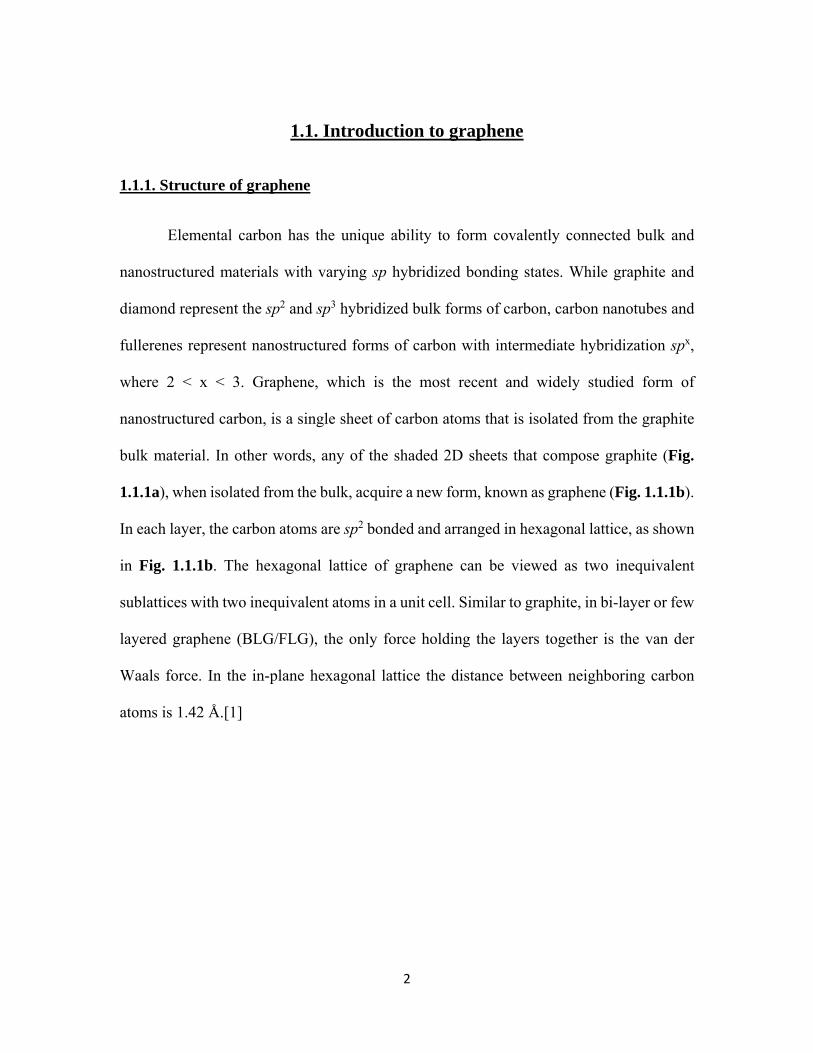
superimposed on the rectangular shaped EDLC response. Fig. 2.1.4a shows a
voltammogram of 10mM K3Fe(CN)6 in aqueous 0.1 M NaCl solution at a Pt working
electrode, the cell setup is three electrode with a Pt counter and an Ag/AgCl reference
electrode. These peaks are signature of charge transfer reactions between the working
electrode and the electrolyte, which occurs at the surface of the electrode.
27
Figure 2.1.4: a) A cyclic voltammogram of 10 mM K3Fe(CN)6 at a Pt working electrode
in aqueous 0.1 M NaCl solution. b) Schematics of the reduction/oxidation process of
species from electrolyte during CV. (Figure from Ref. [28])
Since in a three electrode setup, the reference electrode has a constant makeup, its
potential is fixed. Therefore, any changes in the cell are ascribed to the working electrode.
We say that we observe or control the potential of the working electrode with respect to
the reference, and that is equivalent to controlling the energy of the electrons within the
working electrode. In Fig. 2.1.4a, the potential of the working electrode is first raised from
-0.2 to 0.6 V, or the voltage is swept in the positive direction which reduces the energy of
the electrons, i.e., the Fermi level of the working electrode is lowered. As shown in Fig.
2.1.4b, at a particular potential, the Fermi level of the working electrode reaches the value
of the highest occupied molecular orbitals (HOMO) of species A in the electrolyte, and
electrons will transfer from A to the electrode, resulting in an oxidation of A to A+ as well
as the appearance of peak in the current signal. Similarly, when the potential is driven

28
negatively from 0.6 to -0.2 V, the Fermi level of the working electrode increases and
matches with the lowest unoccupied molecular orbitals (LUMO). At this potential
reduction species A is reduced from A+ to A and is accompanied by the appearance of a
valley in CV. In the example of Fig. 2.1.4a, the species A/A+ refers to Fe(CN)64-/Fe(CN)6
3-.
The peak/valley in CV correspond to one reduction/oxidation reaction, and is defined as a
redox couple. A redox couple in CV provides a lot of information for studying
electrochemical reactions, such as determining the formal reduction potential and the
reversibility of the reaction, calculating the equilibrium ratio, predicting the possible
reaction as well as the intermediate reaction states, etc. [29] Therefore, CV has been widely
used in the characterization of pseudocapacitors,[30] batteries,[31] biomolecular
interactions,[32,33], etc.
2.1.3. Charge-discharge
In a charge-discharge measurement, the electrochemical cell is galvanostatically
cycled at a fixed current density between the highest and the lowest voltage limits. It is a
method which has been widely used to determine the cycle-life as well as capacitance (or
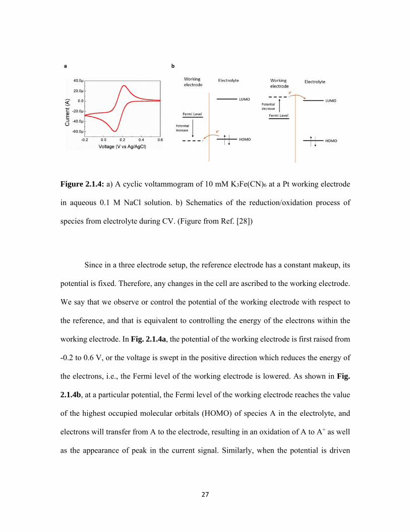
capacity) of EDLCs or batteries.[31] A typical charge-discharge curve of an EDLC device
in a two electrode setup with two symmetric carbon electrodes is presented in Fig. 2.1.5.
29
Figure 2.1.5: Charge-discharge curve of an EDLC device with two symmetric electrodes
made of multiwall carbon nanotubes in 1 M HClO4 aqueous electrolyte. Current density:
50 A/g.
In a system with no electrochemical reaction, the voltage increases/decreases
linearly with time during the charge/discharge process. The specific capacitance of the
EDLC device can be calculated from the slope of the discharge curve:
| | , (2.3)
where I is the discharge current density.

30
It is noteworthy that a voltage drop ΔV between the end of the charge cycle and the
beginning of the discharge cycle may be present. This voltage drop can be used to calculate
the equivalent series resistance (ESR) of the cell as
∆ /∆ . (2.4)
In the equation ∆ is the change of current density from charge
to discharge.
From Eqs. 2.3 and 2.4, the energy density E as well as power density P of the EDLC
can be estimated from the charge-discharge results as
, (2.5)
. (2.6)

31
Figure 2.1.6: Charge-discharge curves of a Li-ion coin-cell battery (half cell) with lithium
iron phosphate as cathode material and Li metal as the anode. Electrolyte: 1 M LiPF6 in
1:1 Ethylene carbonate and diethyl carbonate organic solvent. Schematic shows the
measurement setup for the cell.
Figure 2.1.6 shows a charge-discharge curve of a Li-ion battery with lithium iron
phosphate as cathode material and Li metal as the anode. In the schematic shown in Fig.
2.1.6, a fixed current density is applied and the voltage is measured as shown. Due to the
electrochemical reaction, the voltage of the cell does not change linearly with time. The
plateaus on the charge/discharge curves corresponding to the oxidation/reduction of the
ions at the cathode. The charging/discharging capacity of the battery is calculated by
multiplying the fully charge/discharge time by the applied current density. It is also simple

32
to calculate the energy density E and power density P from the charge/discharge curves of
a battery as
, (2.7)
/ . (2.8)
In the Eq. 2.8, with a fixed current density, V denotes the nominal voltage which
is measured at the midpoint between fully charged and fully discharged states. Q is the
capacity which the battery delivers, and t is the time used to fully discharge the battery.
2.1.4. Electrochemical impedance spectroscopy
When a circuit consists of elements which are not purely Ohmic, the current
response does not change linearly with applied voltage due to the phase shift, and hence
the system is non-linear (Fig. 2.1.7a). The impedance of the non-linear system is in a
complex form, and frquency dependent. Electrochemical impedance spectroscopy (EIS) is
a powerful tool to accurately unravel the non-linear processes and to study the dynamics
of the electrochemical cells.

33
Figure 2.1.7: a) Phase shift between current and applied AC voltage in a non-linear system.
b) In an EIS measurement, a small AC perturbation dV is applied. The AC current response
of the circuit is phase shifted relative to that of dV, which results in the ellipitical shape
shown in the panel b. The brown dash line clearly shows the non-linear current dependence
to the DC voltage. However, when the investigated voltage range V is small enough (in
range of dV), the DC current vs voltage curve can be considered as pseudo-linear. c, d) EIS
may be present in two forms: c) Bode plot and d) Nyquist plot.

34
EIS measurements are usually carried out by applying a small AC perturbation
signal with a fixed applied DC voltage to an electrochemical cell. The frequency of the
perturbation signal is changed and the current through the cell is recorded. The amplitude
of the AC signal is small enough so that the response of the cell can be considered as
pseudo-linear (see Fig. 2.1.7b). As shown in Fig. 2.1.7a, for an electric circuit with
complex form of impedance ", the response of its current, I sin ,
exhibits a phase-shift relative to the applied voltage signal sin . It can be seen
from Eq. 2.9 that both the real and the imaginary parts of the impedance are frequency
dependent and can be written in the form of Eq. 2.10 as
, (2.9)
" cos sin . (2.10)
EIS typically has two output formats, while the Bode plots consist of two plots of
the magnitude of impedance versus frequency as well as the phase angle versus
frequency, the Nyquist plot is a plot of " versus ′ (see Figs. 2.1.7c and d). An EDLC
cell can be simply modeled by the Randles cell circuit (schematic in Fig. 2.1.8a).

35
Figure 2.1.8: a) Schematic of Randles cell circuit. b) Theoretical Nyquist plot for Randels
cell.
In Fig. 2.1.8a, the element RΩ refers for the uncompensated resistance contributed
by the wires, connections, resistance from the electrode materials as well as the solution.
Cdl is the double layer capacitance and Rp is the polarization resistance attributed by the
transition resistance between the electrode and the electrolyte. The impedance of the
Randles cell is expressed as
, (2.11)
from which it follows that
, (2.12)

36
" . (2.13)
Clearly from Eqs. 2.12 and 2.13, the Nyquist plot of the Randles cell is a semicircle
as shown in Fig. 2.1.8b. In the Randles cell circuit, the impedance from the element Cdl is
frequency dependent which varies as ~ . At high frequency the impedance of Cdl is
close to zero and it acts as a short, which and leaves only RΩ contribution to the total
impedance. Also, the impedance of Cdl approaches infinity with frequency decreases and
acts as an open circuit at low frequency. Therefore, the total impedance is equal to the value
of RΩ + Rp at the low frequency end, and the imaginary part of Z is zero at both high
frequency and low frequencies.
Figure 2.1.9: a) Schematic of Randles cell circuit including Warburg impedance. b) A
Nyquist plot of a multiwall carbon nanotube electrode. The diagonal response whcih
appears at the low frequency end of the semicircle is due to ion diffusion. Electrolyte: 1 M
TEABF4 in acetonitrile.

37
A more precise equivalent circuit can be used for modeling the EDLC cell by
adding a Warburg diffusion element to the Randles cell in series of Rp (See Fig. 2.1.9a).
The Warburg impedance is due to the diffusion of ions and is also frequency dependent
(see Eq. 2.14).
/ 1 . (2.14)
The Warburg impedance is small at high frequency since the diffusion path of ions
are short. However, it increases at low frequency because the ions have to move further,
which results in the appearance of diagonal response at the low frequency end of the
semicircle (see Fig. 2.1.9b).
EIS has been frequently used for analyzing the resistance and diffusion information
in capacitors and batteries.[34–37] Moreover, as it has variety of output formats and is
applicable to many forms of electric circuit models, it is also considered as the most
powerful and accurate method which has been applied in multiple areas such as diagnosing
equivalent circuit,[38] investigating corrosion rate,[39,40] characterizing deposition
mechanism,[41] studying the chemical reaction mechanism,[42] chemical synthesis,[42]
semiconductors,[38,43], etc.

38
2.2. Raman Spectroscopy
2.2.1. Introduction of Raman
When a monochromatic light is shone on a medium (which could be in the form of
a liquid, solid or gas), the scattered light is found to be shifted in energy when compared
to the incident light energy. This phenomenon, which has been called the Raman effect, is
attributed to the inelastic scattering of light from the medium. The inelastic scattering
results from the interaction between the incident photons and the vibration of the molecules
in the media, as shown schematically in Fig. 2.2.1a. The Raman effect was theoretically
predicted by Adolf Smekal[44] and experimentally observed by Sir C. V. Raman[45].
In a Raman scattering experiment, the incident light (typically a monochromatic
laser beam) is incident on the sample. Viewed in terms of energy levels, the electrons reside
in the ground vibrational and electronic states before excitation. The monochromatic laser
source excites the electrons to a virtual state, equal to the energy of the laser. When the
electrons relax back to the ground electronic state, most go back to the ground vibrational
state, giving back the same energy. This is Rayleigh (elastic) scattering. The other small
portion that relaxes back to an upper or lower vibrational state is the Raman scattered light.
The Raman scattered light that is adjusted up in wavelength is called the Stokes Raman
scattering and that light which is adjusted down in wavelength is called the anti-Stokes
Raman scattering (Fig. 2.2.1b). Stokes Raman scattering occurs when some energy is
absorbed from the photon of the incident light into the molecule’s rotational and vibrational
energy and consequently a new photon of light with less energy is released. Anti-Stokes

39
scattering occurs when the new photon formed gains energy compared to the incident
photon via the absorption of energy from a previously excited molecule. [46]
Figure 2.2.1: a) A schematic of incident light interacting with molecules, which results in
elastic and inelastic scattering. b) Processes of Stokes and anti-Stokes scattering.
Fig. 2.2.1b demonstrates the Stokes and anti-Stokes processes, which are shifted in
frequency relative to the incident laser energy. On the other hand, the Rayleigh scattered

40
light has same frequency as that of the incident laser and can be filtered out using a notch
filter. Fig. 2.2.2 shows Raman spectrum of sulfur with exciting laser wavelength 1064 nm.
The anti-Stokes scattering has much less cross-section than that of the Stokes scattering,
owing to the fewer probabilities of the existence of the excited molecules.
Figure 2.2.2: Raman spectrum of sulfur with exciting laser wavelength 1064 nm. The
peaks with positive/negative Raman shift are from Stokes/anti-Stokes scattering. It can be
seen that the (i) frequency positions of the anti-Stokes peaks are symmetric to those of the
Stokes peaks, and (ii) intensity of anti-Stokes peaks are much weaker compared to the
Stokes peaks.

41
Clearly, Raman spectroscopy provides information of molecular vibration, which
can be used as a “fingerprint” to identify materials and to analyze the molecule structure,
symmetry, or chemical bonds. In addition, Raman spectroscopy is not moisture sensitive
and can be performed easily under ambient conditions. Raman spectroscopy has evolved
into an indispensable characterization tool for graphene, which will be introduced in next
section.
2.2.2. Phonon dispersion in graphene
The phonon dispersion relation provides a full picture of the molecular vibration of
graphene, as shown in Fig. 2.2.3. As introduced in Chapter 1, graphene has two atoms in
each of its unit cell. Each atom contributes 3 phonon branches. Therefore, there are totally
6 phonon branches of graphene. Three of the phonon branches are acoustic, which are
denoted as: longitudinal acoustic (LA), in-plane transverse acoustic (iTA) and out-of-plane
transverse acoustic (oTA). Similarly, the other 3 phonon branches are optic and they are
denoted as longitudinal optic (LO), in-plane transverse optic (iTO) and out-of-plane
transverse optic (oTO).[47] Starting from the center of the Brillouin Zone (BZ) (i.e., the Γ
point), the momentum of the phonon vary from 0 to , here a0 refers to the length of the
unit vector in the graphene lattice, and equals to√3 ~ 0.26 nm.

42
Figure 2.2.3: a) Brillouin zone of graphene in which the center point Γ is the point where
momentum is zero. b) The phonon dispersion relation of graphene. [48]
The momentum of a photon is equal to , where λ is the wavelength of the light.
The laser light that is used in a typical Raman experiment is usually in range of visible or
IR light with wavelength ranging from ~ 200 to 1100 nm. Therefore, the momentum of the
photons are much smaller than that of the maximum dimension of graphene’s BZ.
Considering the momentum conservation law, the only allowed modes that could be
detected by Raman spectroscopy are phonons with momenta close to the Γ point, or zone-
center phonons. Since acoustic phonons have nearly zero energy at the Γ point, and the
oTO phonon mode is not Raman active, according to the phonon dispersion relation in Fig.
2.2.3b, only one peak is expected in graphene’s Raman spectrum ~ 1600 cm-1, which
corresponds to the doubly degenerate LO and iTO phonon modes at the Γ point.

43
Figure 2.2.4: a) Raman spectrum of a CVD grown single layer graphene at room
temperature, the laser wavelength is 532 nm. b) Schematic of the Raman process for the
G-band in graphene.
From the Raman spectrum of the single layer graphene (Fig 2.2.4a), clearly a
dominant peak ~ 1580 cm-1 is present, which matches with our prediction. This band is
denoted at graphitic band, or G-band. Fig. 2.2.4b presented the schematic of the G-band
Raman process. The electrons from ground state were first excited by the incident photon
to an excited state (represented by the green arrow). The excited electrons are then
scattered by a phonon (with zero momentum) which carry away a portion of the energy to
the electrons. Consequently, the electrons relax to their original state and emit a photon

44
with less energy (Stokes scattering). Nevertheless, in addition to the G-band, additional
peaks are also present in Fig. 2.2.4. These peaks are the so-called D-band ~ 1350 cm-1, G’-
band ~ 2700 cm-1, D’-band ~ 1610 cm-1, G*-band ~ 2450 cm-1, and so on [47]. These peaks
do not match with any phonon branch at the Γ point and seem to violate the law of
momentum conservation. As explained in next section the origin of these additional peaks
can be understood within the framework of the double-resonance (DR) Raman process.
2.2.3. Double-resonance process in graphene
In a typical Raman scattering process, there are normally three steps: i) the incident
light excites electrons from the valence band of the medium to a state with higher energy
(the state could be either a real or a virtual state). ii) the excited electrons interact with
phonons in the medium and emit or absorb phonons, and iii) the electrons relax back to the
valence band by emitting a photon. In the above process ii), if the excited electron happens
to be in a real energy state before or after its interaction with the phonons, a resonant Raman
scattering occurs, and the scattering cross-section can be >103 times larger than that of the
non-resonance Raman scattering.[49] Thus, resonant Raman spectroscopy is well suited
for characterizing samples which are available in limited quantity.[50] However, typically
limited laser excitation energies as available, which prevents the possibility of
characterizing all materials through resonance Raman scattering.
As discussed in Chapter 1, graphene has non-zero band gap at the K and K’ points
in its electronic band structure, and exhibits a linear dispersion above and below its Fermi

45
level. This unique electronic band structure allows the possibility of probing graphene
through resonant Raman scattering with any incident excitation. In graphene, the G-band
originates from a first-order process, as previous explained in Fig. 2.2.4b. There could also
be higher-ordered Raman processes, which allows the excited electrons to interact with
phonons with momentum q ≠ 0 without violating the momentum conservation law. For
instance, in a second-order process, an excited electron could at first interact with a phonon
with momentum q, following by another interaction with a phonon with momentum of –q.
The chance of higher-order Raman processes are very limited unless they match the
resonance conditions. Hence, in graphene, a material with electronic band structure that is
conducive for resonant Raman process, we can expect to see higher-order Raman bands.
In Figure 2.2.3, peaks D, D’ and G’ are known to come from second-order resonance
Raman processess, which is also called DR Raman process.
Figure 2.2.5: a, b) The intervalley double-resonance picture of a) G’-band, b) D-band. c)
The intravalley double-resonance picture of the D’-band.
46
The G’ band has the highest intensity and originates from a two-phonon double
resonance process. From Fig. 2.2.3b, one can notice that the peak position of G’-band ~
2700 cm-1 , which is twice the frequency of the iTO phonon near K point (i.e. phonon
momentum q ~ ). Indeed, G’ is an overtone of two iTO phonons with q ~ due to an
intervalley DR process (see Fig. 2.2.5a).
The D-band, which has frequency equal to one iTO phonon near the K point also
originates from the intervalley DR resonance (Fig. 2.2.5b) in which the excited electron
experiences one inelastic scattering by the iTO phonon with moment q ~ followed by
another elastic scattering by a defect, with momentum -q. It is important to note that the D-
band manifests in the Raman spectrum only when defects (missing carbon atoms, dopants,
etc.) or edges (zig-zag edges) are present in graphene. The intensity ratio of D-band to G-
band is inversely proportional to the average in-plane crystal size of graphene [51] and can
be expressed as
La (nm) = (2.4 × 10⁻¹⁰ nm-3) λ4laser (nm4) (ID/IG)−1 . (2.15)
Therefore, ID/IG had been widely used for identifying the defect concentration and the
quality of graphene.
Another defect dependent peak in the Raman spectrum of graphene is the D’-band
which is found next to the G-band. As shown in Fig. 2.2.5c, the D’-band comes from an

47
intravalley DR process, involves two scattering events: by an LO phonon with q = 2k and
a defect, respectively.
Beside the above discussesion of zone-centered and off-zone-centered Raman
bands, other weaker Raman peaks with that arise from higher-order processes (combination
or overtone of two or more phonons) have also been reported in graphene [47,52–54]. One
of them is the G*-band ~ 2450 cm-1 whose origin remains unclear, and whose asymmetric
lineshape continues to intrigue carbon researchers. In Chapter 5, we will elucidate the
origin of G*-band, and discuss in detail the role of defects on the G*-band.

48
CHAPTER 3
ROLE OF DEFECTS AND DOPANTS ON THE
ELECTROCHEMICAL PROPERTIES OF GRAPHENE
3.1. Introduction
Supercapacitors (SCs) are novel electrochemical devices that store energy through
reversible adsorption of ionic species from an electrolyte on highly porous electrode
surfaces. SCs are highly durable (lifetime >10,000 cycles) with power densities (10
kW/kg), that are an order of magnitude larger than achievable power density in batteries.
But the low energy density (10 Wh/kg) of SCs[55] relative to batteries limits their use in
practical applications despite their ability to withstand >10,000 cycles. Graphene-based
nanocarbons are ideal electrode materials for SCs due to their low cost, high stability, and
high specific surface area. Indeed, an outstanding characteristic of single-layer graphene is
its high specific surface area of ~2675 m2/g, which sets an upper limit for electrical double
layer capacitance (Cdl) ~21 µF/cm2 (~550 F/g).[55–58] Notwithstanding this desirable
attribute, there are two intrinsic bottlenecks that impede the emergence of high energy
density SC devices: i) typically only 50-70% of the theoretical surface area is accessible to
ionic species present in the electrolyte,[55,56] which limits the overall capacitance (10-15
µF/cm2) and leads to a low energy density, and ii) although the total energy that can be
harnessed from a SC device depends predominantly on ion-accessible surface area, it is not

49
the only factor. The presence of a so-called quantum capacitance (CQ), which is (i) small
and in series with Cdl, and (ii) arises from the low electronic density of states at the Fermi
level (DOS(EF)) for nanocarbon electrodes, overwhelms the high Cdl further reducing the
already limited capacitance and low energy density.[59–61]
While efforts to increase the energy density have been focused either on increasing
the active surface area or the pseudo-capacitance through the inclusion of redox active
materials, pragmatic methodologies to resolve the inherent bottlenecks described above are
still lacking. In this chapter, I experimentally show that engineered defects in graphene can
alleviate these bottlenecks resulting in a new paradigm for energy storage beyond the
predicted theoretical limits.
Defects are often perceived as performance limiters in bulk materials, and this
perception is all the more exacerbated in 2D materials such as graphene. Yet, my
experimental findings conclusively demonstrate that controllably induced defects in
specific configurations can achieve 150% enhancement (~50 F/cm2) in measurable
capacitance of few-layer graphene (FLG). A detailed density function theory (DFT)
calculations performed by my collaborators show that the nitrogen dopants in the pyrrolic
configuration result in a high DOS(EF) and thereby mitigate the influence of CQ.
Furthermore, access by the electrolyte ions (e.g., tetraethylammonium (TEA+) ions) to the
inter-layer gallery space in FLG can be effectively enhanced through defect-induced pores
in graphene, leading to an increased charge storage capacity. More importantly, I show that
these high-capacitances can be extended to coin-cell devices based on FLG foams that

50
result in energy densities that are at least five times higher than the conventional activated
carbon-based SCs.
3.2. Experiment and Calculation Methods
3.2.1. Calculation methods
The geometry optimization of bilayer graphene with electrolyte molecule and the
three types of dopant configurations along with their electron density profiles were
performed using a DFT based atomistic tool kit virtual nano lab.[62] The optimization was
performed at mesh cut off 150 Rydberg. Local Density Approximation (LDA with Perdew-
Zunger) has been used as exchange correlation functional with Double Zeta Polarized basis
set. The structure was optimized until the net force on every atom became less than 0.01
eV/ Å. Sampling of the Brillion zone for structure relaxation was taken as 1x3x3 using
Monkhorst-Pack Scheme.
3.2.2. Synthesis of N-doped few-layer graphene and graphene foam
FLG and graphene foams on Ni substrates were synthesized through a chemical
vapor deposition (CVD) method.[63] Doping of nitrogen atoms in FLG and graphene
foams was achieved during the CVD synthesis by the introduction of benzylamine and
acetonitrile in varying proportions to yield the pyridinic, pyrrolic, and graphitic
configurations in FLG (see schematic in Figure 3.2.1). Ni foils with thickness of 25 μm
51
were placed away from the center of a 24 mm diameter tube furnace. The furnace was
maintained at 900 °C under a flow of 200 sccm Ar and 120 sccm H2. Ni foils were moved
to center of the furnace after 90 minutes, and the furnace was reset to 850 °C. Under these
CVD conditions, decomposing ~10 sccm of methane for 10 min yielded the FLG on the Ni
foils. To dope FLG with nitrogen, additional Ar (~50 sccm) was bubbled through a mixture
of benzylamine and acetonitrile (3:1, 1:1, and 0:1 for samples N1, N2, and N3,
respectively), as shown in Fig. 3.2.1. After 10 mins, the methane flow was switched off
and the samples were moved away from the center of the furnace, and the furnace
temperature was ramped down to 400 °C at a rate of 5 °C/min. Next, the H2 flow was shut
off and the furnace was maintained at 400 °C for an additional 90 min. Finally, the samples
were cooled to room temperature under Ar flow. For each N-dopant configuration, at least
three sister samples were used in our spectroscopic studies. FLG samples were also Ar+
plasma etched using a reactive ion etching unit (Hummer 6.2) at multiple powers from 10-
120 W for 2 min to induce defects. Dopant and defect concentration were quantified using
Raman spectroscopy and X-ray photoelectron spectroscopy.

52
Figure 3.2.1: Schematic of the CVD setup for the growth of pristine and N-doped graphene.
The inset figure shows the pyridinic, pyrrolic, and graphitic configurations in which
nitrogen atoms are incorporated into the graphene lattice. [64]
The pristine graphene foams (GFs) used in this study were grown on Ni foams using
the thermal CVD method, similar to the FLG. After the growth of GFs on Ni foams, the
latter were etched away by submersing the GF/nickel foam in a 1:4 (by volume) 12 M
hydrochloric acid: 15.8 M nitric acid solution. The free-standing GF was then rinsed with
DI water and allowed to dry. Some of these GFs were also subjected to a 120 W Ar+ plasma
for 2 minutes at 120 mtorr. Post nitrogen doping of free-standing GFs was accomplished
by annealing them in a tube furnace at 600°C for 1 hr under a 500 sccm flow of argon
which was bubbled through acetonitrile.

53
3.2.3. Structural and electrochemical characterizations
A Dilor XY triple grating monochromator was used for collecting the micro-Raman
spectra of all samples with the 532 and 633 nm excitation. X-ray photoelectron
spectroscopy (XPS) studies were performed using a Kratos Axis Ultra DLD instrument
and spectra were calibrated by the C 1s line at 284.6 eV. The morphology of the samples
was observed using scanning electron microscopy (SEM, Hitachi S4800) with an
accelerating voltage of 20 kV and tunneling electron microscopy (TEM, Hitachi H9500).
The electrochemical properties of samples were characterized in a Gamry reference
3000 electrochemical potentiostat. The electrolytes were 0.25 M tetraethylammonium
tetrafluoroborate (TEABF4, >99%) or tetrabutylammonium hexafluorophosphate
(TBAPF6, >99%) in acetonitrile (ACN). Two systems were used for electrochemical
characterization: a 3-electrode setup for single electrode characterization, and a 2-electrode
cell (coin cell apparatus, MTI Corp) for symmetric supercapacitor measurements. In the 3-
electrode cell, the FLG on Ni foils were used as working electrodes, a Pt mesh was used as
the counter electrode and a silver/silver ion electrode (Ag/Ag+) was used as the reference
electrode. In the 2-electrode cell, EDLC devices were tested using symmetric GFs as the
electrodes with a Celgard (2325) trilayer separator. The electrodes and separator were
soaked overnight (~20 hours) in 0.25 M TEABF4-ACN electrolyte prior to the cell
assembly. Cyclic voltammetry (CV) was measured from -0.4 to 0 V (0 – 2.5 V) for FLG
(GF) samples with scan rate of 1000 mV/s. The electrochemical impedance spectroscopy

54
(EIS) measurements were carried out with a perturbation signal of 10 mV in the frequency
range of 100 kHz to 0.1 Hz.
3.3. Effects of ion etching induced defects and type of electrolytes on
electrochemical properties of graphene
3.3.1. Identification of best-suited electrolyte
It has been observed that the best performance of SCs can be realized when the
average micropore size in nanostructured bulk electrodes (e.g., carbide-derived carbon)
matches the size of the ions in the electrolyte[65–73]. It is expected that such a resonant
effect is true even for defect-induced pores in quasi-two dimensional FLG (Fig. 3.3.1a).
Accordingly, in order to identify the best-suited electrolyte, we theoretically studied the
interactions of two different ions – tetraethylammonium (TEA+) and tetrabutylammonium
(TBA+) with defect-induced pores in FLG. The rationale in choosing these ions lies in the
fact that organic electrolytes such as tetraethylammonium tetrafluoroborate (TEABF4) and
tetrabutylammonium hexafluorophosphate (TBAPF6) exhibit a wider voltage range, yet are
not highly expensive unlike the ionic liquids. In our density functional theory (DFT)
calculations, we started with an initial pre-optimized configuration of bilayer graphene
with a 1 nm pore (See Fig. 3.3.2). Upon the introduction of TEA+ ion into the interlayer
spacing through the 1 nm pore, no significant changes were observed in the optimized
bilayer geometry (Fig. 3.3.1b) and the edge carbons did not show any chemical

55
bonding/interactions with the TEA+ ion. However, a large deformation in the structure of
graphene sheets and an increase in the inter-layer spacing was observed in the presence of
TBA+ ion. In particular, we observed that the edge-carbons in the nanopore strongly
interact with TBA+ ion through chemical bonding preventing it from diffusing through the
nanopore (Fig. 3.3.1c). By analyzing the charge density plots, we found that the TBA+ ion
in our simulations loses two H atoms from its methyl group and subsequently attaches to
dangling edge C atoms in the pore through electron sharing C-C bonds. Such an
observation may be rationalized in terms of the relatively larger size of TBA+ (~0.8 nm)
compared to TEA+ ion (~0.45 nm).[35]

56
Figure 3.3.1: The interaction of electrolyte ions with defect-induced pores. (a) Defect-
induced pores in FLG open otherwise inaccessible surface area by transporting electrolyte
ions (e.g., tetraethylammonium (TEA+)) to inter-layer gallery space. Density functional
theory calculations showed that the intercalation of TEA+ is more favorable (b) compared
to tetra-n-butylammonium (TBA+) (c). In (b) and (c) gray, blue, and white spheres
represent carbon, nitrogen, and hydrogen atoms, respectively.

57
Figure 3.3.2: Structure of bilayer graphene before and after optimization.
3.3.2. Experimental validation of ion-pore size resonance effects
We synthesized FLG and graphene foams on Ni foils through chemical vapor
deposition (CVD) using as described above. We used Ar+ plasma etching and N-doping to
induce defects in the FLG.[59] The defect-formation energy for extended defects is much
lower compared to single- and di-vacancies, and thus we observed the formation of
nanosized pores in FLG upon Ar+ exposure (Fig. 3.3.3a). In the Raman spectrum of
graphene, the peak present at ~1350 cm-1 (or the so-called D-band) arises from the presence
of defects such as nanopores, and its normalized intensity has been widely used to quantify
defect density.[59,74] Accordingly, the defects in our FLG were quantified using the
normalized Raman intensity ratio (ID/IG) of the D-band to the graphitic or G-band present
at ~1580 cm-1.[75] We varied the Ar+ plasma power to produce FLG with different defect
densities or ID/IG, and as expected, ID/IG was found to increase linearly with the Ar+ plasma

58
power (see inset of Fig. 3.3.3b). We performed cyclic voltammetry (CV) using a three-
electrode electrochemical cell to study the electrochemical response of different
electrolytes, viz., 0.25 M TEABF4 or TBAPF6 dissolved in acetonitrile (ACN). The
presence of CQ in series with Cdl is expected to result in a total measured capacitance Cmeas=
(Cdl-1+CQ
-1)-1. We found that Cmeas in defected FLG increased for either electrolyte, which
may be rationalized in terms of the higher CQ (= e2*DOS (EF), where e is 1.6 x 10⁻¹⁹ C),
resulting from a dopant-induced increase in DOS(EF).[59] Although Cmeas increased for
either electrolyte, TEABF4 showed a much higher enhancement than TBAPF6 (almost
twice for the highest defect concentration). Such an observation concurs with our DFT
calculations, which showed that TEA+ ions are more suitable for accessing the interlayer
spacing in FLG through nanopores. It should be noted that the nanopores in plasma-treated
FLG (Fig. 3.3.3a) are sufficiently large to allow both TEA+ and TBA+ ions. However, the
relatively smaller size of TEA+ (0.45 nm) compared to TBA+ (~0.8 nm) facilitates easier
access to the inter-layer space in FLG, resulting in a higher capacitance.

59
Figure 3.3.3: The experimental validation of DFT results. (a) Transmission electron
microscopy (TEM) images of the nanopores created in FLG by exposure to Ar+ ions for 2
min (power varied from 0 - 120 W). (b) The change in total measured capacitance (Cmeas=
(Cdl-1+CQ
-1)-1) as a function of defect densities (measured by ID/IG ratio, where ID and IG
represent the integrated areas of the Raman D- and G-bands, respectively) for FLG samples
in the presence of: i) 0.25 M tetraethylammonium tetrafluoroborate (TEABF4) in
acetonitrile (blue dots and solid line), ii) tetrabutylammonium hexafluorophosphate
(TBAPF6) in acetonitrile (red squares and dash line). Inset: ID/IG as a function of the Ar+
plasma power shows a nearly linear dependence.

60
3.4. Effects of N-doping on electrochemical properties of graphene
3.4.1. N-doping for improved power and energy density
While the plasma etching of FLG significantly improves the measured capacitance
and the energy density (= 0.5CmeasV2, where V is the voltage), the increased ID/IG
compromises the power density due to an increase in the Warburg resistance (see Fig.
3.1.1). Furthermore, the presence of pores in the graphene severely weakens its structural
integrity and thereby deteriorates the durability of the electrodes, and will be discussed
later in Fig. 3.5.1. Alternatively, the rich chemistry between carbon and nitrogen could be
used to introduce N-dopants into graphene lattice in order to increase CQ, Cmeas, and energy
density similar to nanopores, and yet retain intrinsic electrical conductivity and structural
integrity of graphene. We prepared three different N-doped FLG using the CVD method
(see Section 3.2.2) for achieving SCs with high energy and power densities. As shown in
Fig. 3.4.2a, N-dopants can be found in at least three different configurations, viz., graphitic,
pyridinic, and pyrrolic. We analyzed the configuration stability, electron density, and DOS
profiles (see Fig. 3.4.2b) for all configurations using DFT calculations. We and others
previously showed that all the configurations exhibited positive formation energy values
(i.e., energy released upon the formation of the structure from free atoms) suggesting that
the doped sheets are stable.[62,76] The introduction of the dopants changed the symmetry
of the lattice and resulted in drastically different DOS(EF) for all the three configurations
(Fig. 3.4.2b). Specifically, the DOS(EF) for the pristine sample is negligible due to its semi-
metallic nature while all other samples showed non-zero DOS(EF), with a very high

61
DOS(EF) for pyrrolic configuration. The increase in DOS(EF), in addition to the fact that
the pyrrolic type defects mimic the behavior of nanopores through extended defects (e.g.,
multiple vacancies) is useful for increasing both energy and power density of SC
electrodes.
Figure 3.4.1: Nyquist plots of electrochemical impedance spectroscopy (EIS) for pristine
FLG, Ar+ plasma etched FLG, and N3 (or pyrrolic N-doped graphene) measured from 0.1
Hz to 100 kHz. Electrolyte: 0.25 M tetraethylammonium tetrafluoroborate (TEABF4) in
acetonitrile. Inset: Magnified Nyquist plots for the high frequency region. It can be seen

62
that the plasma etched FLG has slightly higher equivalent series resistance (indicated by
the first intercept of the Nyquist plots on the real axis[77]) and interfacial charge transfer
resistance (represented by the radius of the semi-circle at the high frequency region) from
the high frequency region. Interestingly, the slope of data in the low frequency region,
which depends on the electrolyte diffusion resistance (Warburg resistance Rw), is different
for all three samples.[78,79] The higher slope indicates better ion diffusion within the
electrodes.[56,80] Clearly, the plasma etched samples exhibit high Warburg resistance,
which could be attributed to the tortuous diffusion path of ionic species through defect-
induced pores. However, sample N3 exhibits lower Rw due to the presence of N-dopants in
the pyrrolic configuration.

63
Figure 3.4.2: The influence of N-doping on the electronic density of states. (a) A
schematic of different N-dopant configurations in graphene. The black and red spheres
represent the carbon and nitrogen atoms, respectively. (b) The electron density of states
(DOS) for pristine, graphitic, pyridinic, and pyrrolic graphene (5x5 unit cells) derived from
the density functional theory. The DOS at the Fermi level (0 eV) is negligible for pristine
graphene while it is very high for pyrrolic graphene.
3.4.2. Characterization of N-doped FLG structures
As shown in Fig. 3.4.3, the C 1s line in the x-ray photoelectron spectroscopy (XPS)
data of FLG exhibited a peak maximum at the binding energy of 284.45 eV. Upon N-

64
doping, the C 1s line was observed to broaden and upshift (0.15–0.35 eV). The presence
of different doping configurations was confirmed by deconvolution of the N 1s line using
Voigtian components. The peak located at 401.7 eV (Fig. 3.4.3b) is identified with
substitutionally doped nitrogen in the graphitic bonding configuration (in sample N1-N3).
The peaks present at 398.6 (in sample N1 and N2) and 400.1 eV (in sample N3) arise from
nitrogen bonded in the non-graphitic configuration, and were previously attributed to
pyridinic and pyrrolic doping configurations, respectively.[10] Based on our XPS studies,
we estimated the N-dopant concentrations in our samples to be ~2 at.%. Although the
samples N1-N3 have all three dopant configurations (viz., graphitic, pyridinic, and
pyrrolic), it should be noted that graphitic (/pyrrolic) configuration is predominant in N1
(/N3). We found that both pyridinic and graphitic configurations are predominant in N2. In
addition to XPS confirmation, the Raman spectrum of N-doped graphene (Fig. 3.4.4)
showed clear evidence for intense D & D'-bands for N2 and N3 samples, unlike the
graphitic dopants in N1, due to the presence of extended defects and vacancies. Previously,
we showed that the electron and phonon renormalization in N-doped graphene increases
the Fermi velocity (vF) and thereby influences lattice vibrations locally near a dopant.[10]
Indeed, a combination of micro-XPS and micro-Raman spectroscopy revealed that the
local renormalization effects in N-doped graphene resulted in an effectively downshifted
Raman 2D band (Fig. 3.4.5) with a large shift for N2 and N3 samples and a negligible shift
of N1 in agreement with our previous studies. [10]

65
Figure 3.4.3: X-ray photoelectron spectroscopy for pristine and N-doped graphene, a) C
1s line, and b) N 1s line.

66
Figure 3.4.4: The D and D’-bands for pristine and N-doped few layer graphene (grown
using chemical vapor deposition) at excitations a) 532 nm and b) 633 nm.
The D and D′ bands are intense for samples N2 and N3 (non-graphitic doping
configuration). The D band for N1 (graphitic doping configuration) is, however, relatively
less intense.

67
Figure 3.4.5: The 2D-band for pristine and N-doped few layer graphene (grown using
chemical vapor deposition) at excitations a) 532 nm and b) 633 nm. The vertical lines in
both panels serve as a guide to the eye. The electron-phonon-renormalization upon doping
leads to a net down-shift in the 2D-band peak position for samples with a non-graphitic
doping configuration. The traces below each spectrum indicate the deconvoluted peaks
used for fitting. Clearly, sample N1 retains intense peaks in the 2D-band with little
downshift at both excitations.

68
3.4.3. Electrochemical characterization of N-doped FLG
For elucidating the influence of dopant configuration on Cmeas, we performed CV
measurements on the pristine, N1, N2, and N3 samples in the three-electrode setup with
previously identified 0.25 M TEABF4 in ACN. As shown in Fig. 3.4.6a, the absence of
redox peaks in the CV plots indicate the lack of specific reactions and pseudocapacitance
arising from charge transfer at the N-doped graphene /electrolyte interface. Clearly, we
observed that the Cmeas values for N-doped FLG were higher than that of pristine FLG, and
sample N3 (pyrrolic) was significantly different from samples N1 and N2, as predicted by
our DFT calculations (see Fig. 3.4.6b). We measured at least 5 different sets of samples to
confirm the results presented in Fig. 3.4.6. The controlled growth of a specific dopant
configuration is highly difficult. Thus, to validate the hypothesis that the increase in Cmeas
originates from pyrrolic configuration, we annealed the plasma etched FLG samples with
nanopores in a 1” quartz tube furnace at 400 °C for 1 hr in Ar bubbled through ACN (see
Section 3.2.2 for more details) into the furnace, or only Ar. We found that the Ar-annealed
FLG exhibited a slight decrease in Cmeas due to a decreased ID/IG upon annealing, as shown
in Fig. 3.4.7. However, Ar-ACN annealed FLG showed a marked increase in Cmeas and
concomitant decrease in resistivity due to the introduction of N-dopants. It is noteworthy
that pristine FLG annealed in Ar or Ar-ACN did not show any changes in Cmeas suggesting
that the initial defects in the form of nanopores facilitated the introduction of N-dopants.
Our detailed XPS characterization of Ar-ACN samples also revealed the presence of non-
graphitic dopants similar to CVD grown samples (see Fig. 3.4.8). Specifically, we observed

69
the presence of N-dopants in pyrrolic and pyridinc configurations, which resulted in
increase of DOS(EF) similar to CVD grown N-doped samples (N1-N3).
Figure 3.4.6: N doping leads to increased capacitance. (a) Cyclic voltammetry (CV)
curves (normalized by scan rate = 1000 mV/s) for pristine and different N-doped FLG
obtained in 0.25 M tetraethyl ammonium tetrafluoroborate (TEABF4) in acetonitrile. b)
The total value of Cmeas for different FLG structures derived from (a).

70
Figure 3.4.7: The change in total measured capacitance (Cmeas) as a function of Ar+ plasma
power for FLG, Ar annealed FLG and Ar-ACN annealed FLG in the presence of 0.25 M
tetraethylammonium tetrafluoroborate (TEABF4) in acetonitrile. The numbers 1-4 denote
FLGs treated by plasma power of 0, 12, 28, 50 W respectively, prior to annealing or
electrochemical measurements. Inset: The ratio of intensity of D-band to the intensity of
G-band (ID/IG) as a function of plasma power.

71
Figure 3.4.8: X-ray photoelectron spectroscopy for (a, b) Ar-ACN annealed FLG treated
by 50 W Ar+ plasma etching, and (c, d) pristine and N-doped GFs. We estimated the N-
dopant concentrations in our samples to be ~2.5 at. %.

72
3.5. Realization of high energy and power densities SC devices with
defect-engineered graphene electrode
Building on the improved performance of the N-doped FLGs, we successfully
constructed a coin-cell made of CVD grown graphene foams. It should be noted that SC
devices based on CVD grown graphene have been limited to substrate-based micro-
capacitors.[81,82] For the first time, to overcome this limit for bulk device applications,
we synthesized large quantities of pristine FLG foams on Ni foam using the CVD method
(see Section 3.4.2). The obtained GFs were etched through the Ar+ plasma processing (for
convenience, referred to as PGFs in Fig. 3.5.1) at 120 W for 2 min for inducing nanopores
(cf. Fig. 3.3.3) and subsequently subjected to a post doping process through Ar-ACN
annealing for producing N-doped GFs (NGFs in Fig. 3.5.1). We fabricated symmetric coin
cells with GF electrodes with a polymer separator placed in between the two electrodes.
The GF electrode-separator-electrode sandwiched structures were assembled in a coin cell
apparatus, as shown in the inset of Fig. 3.5.1a. The CV profiles of the as-assembled coin
cells (with three different electrodes viz., pristine GFs, PGFs, and NGFs) with 0.25 M
TEABF4 electrolyte are shown in Fig. 3.5.1a. Clearly, while the PGFs showed a two-fold
increase in Cmeas over pristine GFs, NGFs exhibited a five-fold increase. Galvanostatic
charge-discharge measurements were carried out to calculate the energy and power density
of the coin cells using W = 1/2CmeasV2, where W is the energy density and V is the cell
voltage, and P = dW/dt, where P is the power density and dt is the discharge time. The
charge–discharge characteristics of N-doped GF coin cells at 5 mA/cm2 are shown in Fig.
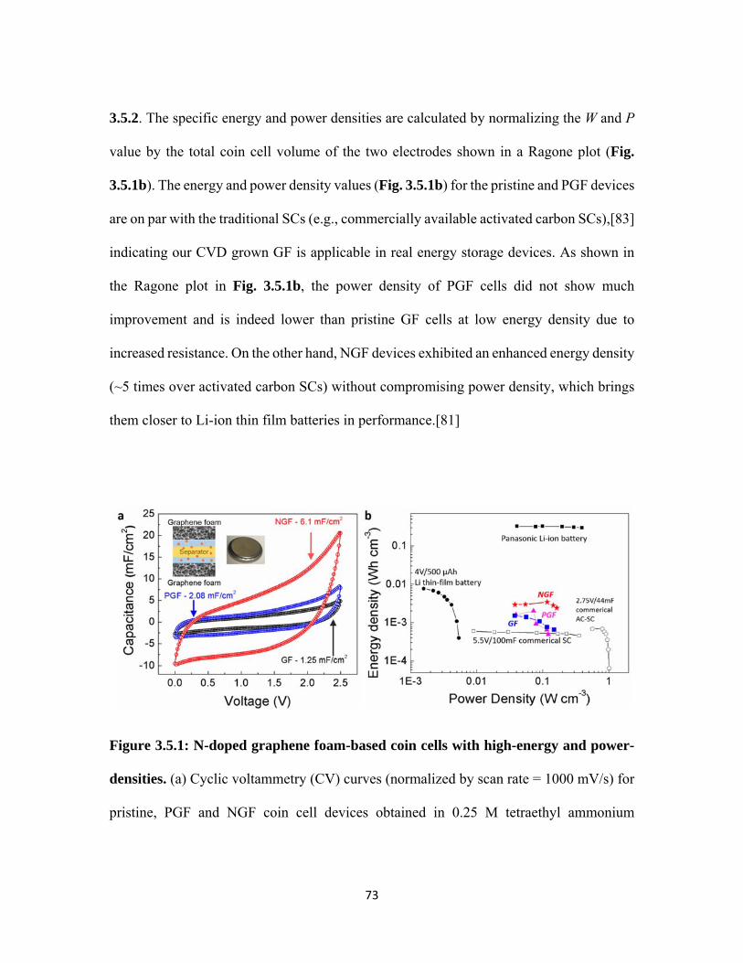
73
3.5.2. The specific energy and power densities are calculated by normalizing the W and P
value by the total coin cell volume of the two electrodes shown in a Ragone plot (Fig.
3.5.1b). The energy and power density values (Fig. 3.5.1b) for the pristine and PGF devices
are on par with the traditional SCs (e.g., commercially available activated carbon SCs),[83]
indicating our CVD grown GF is applicable in real energy storage devices. As shown in
the Ragone plot in Fig. 3.5.1b, the power density of PGF cells did not show much
improvement and is indeed lower than pristine GF cells at low energy density due to
increased resistance. On the other hand, NGF devices exhibited an enhanced energy density
(~5 times over activated carbon SCs) without compromising power density, which brings
them closer to Li-ion thin film batteries in performance.[81]
Figure 3.5.1: N-doped graphene foam-based coin cells with high-energy and power-
densities. (a) Cyclic voltammetry (CV) curves (normalized by scan rate = 1000 mV/s) for
pristine, PGF and NGF coin cell devices obtained in 0.25 M tetraethyl ammonium

74
tetrafluoroborate (TEABF4) in acetonitrile (ACN). (b) Ragone plot comparing the
performance of GF coin cell devices with 0.25 M TEABF4-ACN electrolytes to
conventional supercapacitors, Li-thin film batteries, and other energy storage devices.
[81,83]
Figure 3.5.2: The charge–discharge characteristics of N-doped GF coin cells at 5 mA/cm2.

75
Figure 3.5.3: Graphene foam-based pouch cells for realistic applications. (a-d)
Photographs showing flexible and compact graphene foam based pouch cells with high
form factor and (e, f) high cycle stability. The pouch cells showed only an insignificant
drop in total capacitance <4% after 10,000 cycles and can be used for practical applications
such as LED lighting (g, h).
One of the bottlenecks in the integration of SCs into pocket-sized and compact
instruments has been their form factor [84]. In this regard, flat, thin, and flexible SCs with
rectangular or square in shape are of interest to the industry. As shown in Fig. 3.5.3, we
fabricated flexible and compact pouch cell devices (total capacitance >100 mF) for realistic
applications such as LED lighting using only graphene foams prepared via a scalable CVD

76
process[85] (Figs. 3.5.3a-d). We observed that the performance of the SC pouch cells
comprised of both pristine and doped graphene foams was stable for over ten thousand
cycles (unlike PGFs) with an insignificant drop of <4% in performance (Figs. 3.5.3e and
f).
3.6. Conclusions
Defects are generally perceived as material performance limiters.[86–88] Contrary
to this established notion, we demonstrated that the appropriate defect configuration could
indeed alleviate roadblocks in harnessing the true energy storage potential of FLG. From a
theoretical standpoint, defects in FLG break the crystal symmetry and thereby change the
DOS(EF), which in turn significantly increases CQ.[59] The small CQ is an intrinsic
limitation that impedes FLG-based SCs from delivering high-energy density.[59–61] In
addition to the increase in CQ, the choice of the right electrolyte could enable the transport
of ionic species through nanopores allowing access to otherwise unused interlayer spaces
in FLG. [65–72] In this work, we used a simple plasma etching process to induce defects
in CVD-grown FLG structures and experimentally demonstrated an increase in Cmeas.
Although the Cmeas in defected FLG is increased by 150% (from 21 F/cm2 to ~50
F/cm2)[55], the presence of defects in FLG severely weakens the structural integrity and
compromises the power density. Indeed, we found that the defected FLGs cannot be cycled
beyond 100-500 cycles, which is a serious limitation for SC devices. To overcome this
challenge, we used the rich carbon and nitrogen chemistry to induce N-dopants into

77
graphene lattice. Our comprehensive characterization and theoretical calculations showed
that the non-graphitic dopants increase CQ by changing DOS(EF) and yet retain the
necessary electrical conductivity and structural integrity. In the case of pyrrolic N-dopants,
we achieved a significant enhancement in Cmeas ~56 F/cm2 without using any pseudo-
capacitive materials. The validity of our results is further reinforced by the experiments on
ACN annealed defected FLG structures. The nanopores in defected FLG acted as a site for
incorporating N-dopants into the graphene lattice and thereby exhibited an increase in Cmeas,
conductivity, and durability similar to CVD grown in situ doped N-doped FLGs.
While these results are exciting from a fundamental physics perspective, these
developments would be futile if they cannot be extended to real-time devices with clear
scalable manufacturing strategies. In this regard, we used CVD to synthesize GFs in bulk
quantities and prepared coin and pouch cell devices. We induced pores in GFs through
plasma etching and subsequently annealed them in ACN to achieve NGF-based coin cells
with significantly higher energy and power densities than commercial SC devices. The
CVD growth, plasma etching, and subsequent annealing are amenable for roll-to-roll
production and are already being used for graphene production at industrial scales. Our
results show new ways to tackle the inherent limitations of energy storage in nanocarbons
by increasing CQ and accessible surface area through defect engineering without
compromising the intrinsic properties of graphene, which opens a new paradigm for energy
storage.

78
CHAPTER 4
ROLE OF DEFECTS AND DOPANTS ON THE MAGNETIC
PROPERTIES OF S-DOPED GRAPHENE
4.1. Introduction
Carbon nanomaterials are regarded as one of the best-suited platforms for
spintronics due to their low density, inherently low spin-orbit coupling, and large spin-flip
scattering lengths [89,90]. Ideally, any sp2 carbon system is expected to exhibit
diamagnetic behavior due to the existence of π-electron orbital magnetism [91]. However,
the origin of anomalous ferromagnetic ordering and paramagnetic response in sp2 carbon
systems has puzzled researchers for many decades [92–94]. This unexpected presence of
magnetic ordering in nanocarbons is a major impediment for realizing long spin-flip
scattering lengths required for spintronic applications. Although there have been many
efforts to understand the presence of magnetism in pure carbon-based nanomaterials [95–
100], many of them have been either controversial or irreproducible. This is likely due to
the presence of unintentional magnetic impurities (e.g., residual Fe catalyst particles in
carbon nanotubes), poorly characterized defects, and intrinsic topology (e.g., curvature in
C60 and nanotubes). Graphene, a two-dimensional atom-thick layer of sp2 carbon, is well
suited for elucidating the origin of magnetism due to its fairly simple honeycomb lattice
with unique electronic and optical properties [26,101]. Furthermore, the properties of many

79
carbon nanomaterials (e.g., fullerenes, carbon nanotubes, graphite, and some polycyclic
aromatic molecules) are often theoretically derived from their underlying graphene lattice.
Many theoretical studies have predicted that point defects in graphene exhibit a
non-zero magnetic moment, which can possibly interact with each other resulting in a long-
range ferromagnetic ordering [95–97,102–106]. Nair et al. reported a purely paramagnetic
behavior in highly defective fluorinated and ion-irradiated graphene, implying the absence
of any defect-defect interactions leading to ferromagnetic (FM) ordering [9,107]. On the
contrary, others have observed signatures of FM in defected graphene indicating possible
interactions between defect-induced magnetic moments [108–110]. Collectively, both
intrinsic defects (e.g., vacancies and edges) and extrinsic dopants (e.g., fluorine dopants,
ion-irradiation induced pores, and unintentional magnetic impurities) have been proposed
to increase paramagnetic response of graphene, and in some cases even cause FM ordering
through defect-defect interactions. As we and others have previously shown, the nature of
defects plays a critical role in an unexpected magnetic ordering in many nanostructured
materials (particularly, nanograined oxides) derived from non-magnetic bulk, for example
ZnO [111–114]. Accordingly in this chapter, we report controllably doped graphene
nanoplatelets (GnPs) with sulfur (an extrinsic defect) to tune different magnetic
interactions between intrinsic (e.g., between vacancies) and extrinsic defects (e.g., vacancy
and S-dopant). Our X-ray photoelectron spectroscopy (XPS) studies as well as density
functional theory (DFT) clearly evince the formation of covalent bonds between S dopants
and intrinsic defects. While we observed that pristine GnPs prepared using the chemical

80
exfoliation method exhibited a weak FM ordering due to the presence of intrinsic defects,
we found that the FM ordering systematically decreased with increasing S dopants
suggesting that the interactions between S-dopants and intrinsic defects demagnetize GnPs.
4.2. Experiment and calculation methods
4.2.1. Synthesis of S-doped graphene
Grade M GnPs (xGnP-M-5, 99.95 at. % carbon and 0.05 at. % sulfur, see Table
4.2.1) were purchased from XG Sciences, Inc. (Michigan, USA). Pristine GnPs consist of
short stacks of graphene sheets with an average thickness of approximately 6-8 nm and
average size of 5 µm (see Fig. 4.2.1). The elemental composition of grade M GnPs from
XG Sciences materials safety data sheet are shown in Table 4.2.1. The S-dopded GnPs
were prepared in two steps, chemical exfoliation process and then sulfur doping process.
The schematic of the experimental purcedures are shown in Fig. 4.2.2.
Ingredient CAS # Wt. %
Graphite 7782-42-5 95 - 100
Sulfur, elemental 7704-34-9 1-5

81
Table 4.2.1: Elemental composition of grade M GnPs. Source: XG Sciences materials
safety data sheet.
Figure 4.2.1: Scanning electron micrographs of grade M GnPs XG Sciences, Inc. (a) Bulk
powder, and (b) Single platelet. Source: XG Sciences materials safety data sheet.

82
Figure 4.2.2: Schematic of the synthesis purcedure for preparing S-doped graphene.
In the chemical exfoliation process, as-received GnPs (5 g) were exfoliated in 100
ml of N-Methylpyrrolidone (NMP) for 2 hours using a 1/8” tip sonicator at 120 W, and
then vacuum filtered using a 0.45µm nylon membrane. Subsequently, the collected “cake”
was re-sonicated using a fresh portion of NMP for 6 hours and vacuum filtered. Finally,
the vacuum filtered GnPs were washed in water thrice and oven dried at 130 oC for 24
hours.
In the sulfur doping experiment, three 100 mg samples of the exfoliated GnP
powders were mixed with 99.5% elemental sulfur, (100 mesh, Alfa Aesar) at nominal
concentrations of 1, 1.5 and 3 wt.% of S using a mortar and pestle (labeled as pristine GnP,

83
1wt.% S GnP, 1.5 wt.% S GnP and 3 wt.% S GnP). The mixed GnP-S samples were
vacuum-sealed in quartz tubes (¼” diameter and 6” in length) and annealed in a furnace at
1000 oC for 24 hours. After cooling down to room temperature, the quartz tubes containing
the samples were gently shaken by hand to homogenize the sample, and then reheated again
at 1000 oC for another 24 hours. Subsequently, the furnace was cooled to 440 oC for 2 hrs
and the sealed quartz tubes were partially pulled out of the furnace to facilitate
condensation of any unreacted sulfur at the opposite cold end of the sealed tubes.
4.2.2. Charcterization of structure and magnetic properties
The magnetic properties of samples used in this study were measured using a
Quantum Design® vibrating sample magnetometer (VSM) and a superconducting quantum
interference device (SQUID) magnetometer. The DC temperature dependent magnetic
susceptibility was measured both in zero-field-cooled (ZFC) and field-cooled (FC)
conditions with temperature ranging from 3 to 150 K. A Dilor XY triple grating
monochromator was used for collecting the micro-Raman spectra of all samples with the
514.5 nm excitation from an Ar+ ion laser. XPS studies were performed in a Phi
spectrometer equipped with a monochromatic Al Kα source (1486.6 eV), which has an
overall resolution of 0.5 eV.
The samples were tested for magnetic impurities such as Fe through inductively
coupled plasma mass spectrometry (ICP-MS) measurements (X series II, Thermo
Scientific) using an internal standard containing Li, Y, and In with a detection limit of 0.05

84
ppb (corrected for sample dilution). For the measurements, 10 mg of sample was dissolved
in 10 ml of 70% nitric acid for 24 hrs under constant stirring. Subsequently, HNO3
containing graphene was centrifuged, and the supernatant was removed and diluted into
2% HNO3 for evaluating the presence of Fe impurities.
4.2.3. Calculation methods
The calculations are performed using the projected augmented wave formalism
[115,116] of DFT as implemented in the Vienna ab initio simulation package [117,118].
The exchange correlation potential is approximated by a generalized gradient
approximation using the Perdew-Burke-Ernzerhof functional [119]. The DFT orbitals are
expanded in plane wave basis with a relatively high energy cutoff of 600 eV. The vacancies
and vacancy clusters are modeled in 10 10 1 supercells of the two atom unit-cell of
graphene (lattice constant: 2.468 Å), with a 15 Å vacuum in the vertical direction. We used
a relatively large supercell to reduce the undesired interaction between vacancies and their
images arising from periodic boundary conditions. The reciprocal space is sampled with 5
5 1 k-point mesh equivalent to the 50 50 1 k-point mesh for the two-atom unit cell.
The same density of k-points is used for simulated nano-ribbons with zigzag- and armchair-
edges modeled in 160- and 168-atom computational cells, respectively. All the atomic
configurations are optimized with spin-polarized DFT.

85
4.3. Magnetic properties of pristine and S-doped graphene nanoplatelets
As shown in Fig. 4.3.1, finite areas of hysteresis loops provide a clear evidence for
FM in both pristine and doped GnP samples at 300 and 5 K, with saturation values (Ms)
~0.06 (pristine), 0.017 (1.5 wt.% S GnP), and 0.043 emu/g (3 wt.% S GnP). The FM is
embedded in a large diamagnetic (DM) background (see insets in Figs. 3.3.1a and b), which
arises from the underlying graphene lattice. Although graphite/graphene is diamagnetic,
the presence of defects (as it will be discussed later) induce weak FM, similar to
nanograined oxides [111–114]. The observed saturation of FM at relatively low fields (~1.2
kOe at 300 K) for both pristine and doped samples indicates: i) the presence of moderately
large spin-clusters, and ii) that the average size of spin-clusters was not affected by doping.
The magnetic coercivity (Hc) increased significantly for all samples at 5 K (see Table
4.3.1) implying that room temperature thermal activation energy ~25 meV is sufficient to
induce spin-flip in all GnP samples. Interestingly, the percent increase in Hc at 5 K (relative
to Hc at 300 K) is highest for pristine samples (~250%) and considerably small in doped
samples (~20%). Such observations, when juxtaposed with our DFT calculations, could be
attributed to dopant-induced passivation of thermal spin fluctuations in unsaturated edge-
states of GnPs. Lastly, we observed a non-monotonic decrease of Ms in S-doped samples
(see Table 4.3.1) confirming that the S-dopants demagnetized GnP samples. Our detailed
ICP-MS analysis (Table 4.3.2) confirmed that the magnetic response (shown in Fig. 4.3.1)
is not from magnetic impurities such as Fe, which were found to be < 20 ppb in both pristine
and doped samples.

86

87
Figure 4.3.1: M-H curves for graphitic nanoplatelets (after accounting for the background
diamagnetism) with various S doping concentration measured at (a) 300 K, and (b) 5 K.
The insets show the as-measured M-H data.
T = 300 K T = 5 K
Pristine
GnP
1.5
wt.%S
GnP
3.0
wt.%S
GnP
Pristine
GnP
1.5 wt.%S
GnP
3.0 wt.%S
GnP
MS (10-2
emu/g) 7.3 1.7 2.6 10.6 4.0 4.3
Mr (10-2
emu/g) 1.8 0.9 0.9 4.0 1.5 1.7
Hc (102 Oe) 1.6 4.6 3.5 5.7 5.5 4.3
Table 4.3.1: The value of saturated magnetization MS, remnant magnetization Mr and
coercivity Hc for pristine, 1.5 wt.% and 3.0 wt.% S doped GnPs under 5 K and 300 K
obtained from hysteresis loops. The non-monotonic variation of MS could result from
sample-to-sample variations, and does not affect our conclusion that S-dopants
demagnetized GnP samples.

88
Pristine GnP 1.5 wt.%S GnP 3.0 wt.%S GnP
Iron concentration
(ppb) 17.73 9.39 12.17
Table 4.3.2: ICP-MS analysis of pristine and doped graphene showed only ppb levels of
Fe contained in all samples ruling out Fe impurities as a possible cause for the observed
magnetic response.

89
Figure 4.3.2: (a) X-ray photoelectron spectra (XPS) recorded for the C 1s line with a
photon excitation energy of 1486.6 eV for pristine, 1 wt.% S, 1.5 wt.% S as well as 3 wt.%
S GnPs .(b) XPS recorded for the S 2p line with a photon excitation energy of 1486.6 eV.(c)

90
Micro-Raman spectra of pristine and S doped GnPs. The solid traces below each spectrum
represent the deconvoluted fits. (d) The ID/IG values for pristine and S doped GnPs.
All samples exhibited an excellent crystallinity as evidenced by the C 1s peak in
the XPS spectra (Fig. 4.3.2a). The S-dopant concentration was quantified from the relative
photoemission cross-sections for the C 1s and the corresponding S 2p peaks (Fig. 4.3.2b).
We inferred that pristine, 1 wt. % S, 1.5 wt. % S and 3 wt. % S nominal S-doped GnPs
contained 0.05, 0.07, 0.18 and 0.25 at. % substituted sulfur, respectively. We limited our
magnetization studies to pristine, 1.5, and 3 wt. % samples because the S concentration in
the pristine and 1 wt. % S samples were not significantly different (see Table 4.2.1).
Furthermore, our XPS results suggest that S is substitutionally doped, and the other
common forms of S-doping (e.g., SO2H. SO3H) are not dominant. The Raman spectrum
for pristine GnPs exhibited a weak disorder band (D-band) ~1350 cm-1 in addition to the
graphitic band (G-band) ~1585 cm-1(Fig. 4.3.2c). As shown in Fig. 4.3.2d, S-dopants did
not significantly alter the intensity of D-band indicating that no additional structural defects
(e.g., vacancies or Stone-Wales defects) were created during the doping process (will be
discussed later in Fig. 4.4.2). Collectively, magnetization measurements, XPS and Raman
spectra suggest that S-dopants predominantly altered the nature of intrinsic defects without
introducing additional structural defects.

91
Figure 4.3.3: Temperature dependent ZFC-FC data for (a) pristine GnPs, (b)1.5 wt.% S
GnPs, (c) 3 wt.% S GnPs in 10 - 10000 Oe. The down pointing arrows are S-dopant
induced antiferromagnetic features as discussed in the text.
The following salient features can be gleaned from the zero field cooled and field-
cooled (ZFC-FC data; Fig. 4.3.3): (i) the low temperature susceptibility (χ) of the pristine
GnPs is about 9 times and 3 times higher than that of 1.5 wt. % S GnPs and 3 wt. % S GnPs,
respectively, (ii) all samples show very strong temperature dependence in FC cycle - χ(T)
is larger in FC than in ZFC conditions. This is an evidence for the presence of small
superparamagnetic clusters in addition to FM domains, (iii) while the FC dependence of
pristine GnPs (Fig. 4.3.3a) shows a monotonic increase of χ(T) with decreasing

92
temperature, the ZFC data displays a sharp downturn starting at ~ 38 K, likely due to DM
of graphite, (iv) the ZFC data for S doped GnPs exhibit a Curie-like upturn instead of the
DM downturn in pristine GnPs at ~38 K, implying that S-dopants have significantly
changed the magnetic interactions in GnPs, (v) two new features at ~45 and 55 K, indicated
by arrows in Figs. 3.3.3b and c, which appear upon S doping, are possible signatures for
antiferromagnetic domains (Fig. 4.3.4) [110,120]. In fact, we observed that the related
intensity of the local maxima increased with increasing magnetic field (Figs. 4.3.3 d-i),
confirming such a hypothesis, and (vi) lastly, the splitting between ZFC-FC curves
decreased at 10 kOe is consistent with the presence of superparamagnetic clusters in our
samples. Interestingly, we observed that the ZFC curve is slightly above the FC (Figs. 4.3.3
g-i), which may be attributed to magnetostriction [121]. As evident from Fig. 4.3.3, the
temperature dependence of χ in S-doped graphene presents several rich and intriguing
features, which will be discussed in a separate publication. Nonetheless, in summary, our
experimental data suggests that more than one type of magnetic behavior can arise from
doping and defects in graphene. Indeed, it is evident that GnP samples exhibit a
combination of superparamagnetic, ferromagnetic, anti-ferromagnetic (all arising from
defects), and diamagnetic (from graphite) domains making GnP a complex magnetic
system to be analyzed.

93
Figure 4.3.4: ZFC-FC curves for pristine GnPs ranging from 3 to 300 K. Inset: Inverse
susceptibility vs. temperature from the FC data (soild black squares), shows linear behavior
with a negative Curie – Weiss temperature ~ -179 K, indicating the presence of some
antiferromagnetic domains.
4.4. Spin-polarized DFT calculations
To further elucidate the origin and dopant-induced changes in the magnetic
properties of GnPs, we performed detailed spin-polarized DFT calculations. Figs. 4.4.1a-
e represent magnetic structures in defected pristine graphene with multiple vacancy

94
configurations. Upon relaxation, the three dangling-bond sites of the mono-vacancy
undergo the Jahn-Teller distortion by breaking the three-fold symmetry, and form a
pentagonal and an enneahedral ring of C atoms (Fig. 4.4.1a) [122,123]. The relaxed
dangling-bond sites constitute an isosceles triangle with two C atoms at the base forming
a weak bond, while the largest magnetic moment is presented at the apex. The calculated
magnetic moment for the mono-vacancy is 1.4 μB and the formation energy is 7.56 eV.
Figure 4.4.1: Magnetic structures in graphene and their local spin density plots: (a) mono-
vacancy, (b) two ferromagnetically interacting mono-vacancies, (c) cluster of three
vacancies, (d) clusters of six vacancies, and (e) zigzag edges. Up and down local spin

95
densities are represented by circles with red and blue shades, respectively. The magnitude
of local moment is represented proportionally to log10 (radius). The net magnetic moment
of each structure is (a) 1.38, (b) 2.91, (c) 0.99, and 0.00 μB for (d) and (e).
Similar to the interactions of other types of local magnetic moments in bulk
materials, the bipartite character is important in magnetic interactions of vacancies in
graphene [124,125]. Multiple mono-vacancies exhibit FM (/anti-FM) interaction if they
are in the same (/different) sublattice of graphene, as seen in Fig. 4.4.1b. Clustering of
multiple vacancies creates a void, and leaves atoms with unpaired electrons (due to
dangling-bonds) along the circumference (Figs. 4.4.1c-d). Large vacancy-clusters can have
many unpaired electrons. However, the net magnetic moment is generally small due to the
anti-FM interaction between two sublattices of graphene. Unpaired electrons in the same
sublattice of graphene energetically prefer the FM interaction, whereas those in different
sublattices favor anti-FM ordering. In the relaxed voids, instant reconstruction of bonds
occurs for some atoms with dangling bonds. Hence, the difference between the numbers of
dangling-bond sites in two sublattices is generally small, typically one to three. In the case
of graphene nano-ribbons, it has been predicted that the zigzag edge exhibits FM ordering
as it contains atoms of only one sub-lattice type [105,126–128]. As shown in Fig. 4.4.1e,
spin moments in GnPs are mainly distributed at the edge carbon atoms, and decay
exponentially into the center of the ribbon.

96
Figure 4.4.2: Optimized bond structures of graphene doped with a sulfur atom (a)
occupying a vacant substitutional site, (b) bridging two carbon atoms along the zigzag edge,
(c) partial double-bonding with a single carbon atom along zigzag edge, (d) bridging two
carbon atoms on the same hexagonal ring along armchair edge, and (e) bridging two carbon
atoms on different hexagonal rings along armchair edge.
Our calculations (Fig. 4.4.2) show that sulfur atoms are strongly attracted to
defected sites of nano-platelets such as vacancy sites and edges, but no adatom-type bonds
between S and graphene are found to be stable. We found that a sulfur atom can fill a mono-
vacancy, saturate dangling-bonds, and become a substitutional defect, Fig. 4.4.2a. The
substitutional sulfur relaxes to a non-planar position with z = 1.1 Å. The binding energy

97
between a sulfur atom and a monovacancy is calculated to be about -6.98 eV, based on
E(binding) = E(substitutional S) E(vacancy) + E(isolated S). Edges of GNPs are also
attractive sites for sulfur atoms. Fig. 4.4.2b-e show various stable bonding structures
between a sulfur atom and zigzag/armchair edges: bridging two carbon atoms on two
neighboring hexagonal rings along the zigzag edge, partial double-bonding with a single
carbon atom along the zigzag edge, bridging two carbon atoms on the same hexagonal ring
along the armchair edge, and bridging two carbon atoms on different hexagonal rings along
the armchair edge. Binding energies of these bonding structures are < −3.8 eV, indicating
strong attachments of sulfur atoms to edges. The C-S bond lengths in our relaxed structures
are in good agreement with the literature values of 1.82 Å for single and 1.72 Å for partial
double bonds [129]. The circumferences of voids in the clusters of multiple vacancies
provide similar attractive edge-sites.

98
Figure 4.4.3: Demagnetization effect of sulfur in graphene with vacancies. In (a), two
ferromagnetically interacting mono-vacancies are gradually demagnetized by successive
additions of two sulfur atoms. Similarly, local magnetic moments of clusters of vacancies
are quenched by attached sulfur atoms in (b) and (c).
Consistent with experimental results (cf. Fig. 4.3.1), we find that S-doping
suppresses magnetic moments induced by dangling-bonds at vacancy sites in graphene
lattice. As shown in Fig. 4.4.3a, the FM interaction between two mono-vacancies located
within the interaction range (<10 nm [19, 20]), results in a net magnetic moment of 2.9 μB.
Doping with a single sulfur atom that occupies one of the two available vacant
substitutional sites leads to a loss of magnetic moment to 1.2 μB. Additional sulfur atom
occupies the remaining vacant site and completely quenches the magnetism. Similar results

99
are observed for graphene with trivacancy, shown in Fig. 3.4.3b, where a substitutional
sulfur atom leads to a complete loss of magnetic moment from 1.0 μB to zero. Fig. 4.4.3c
shows a special case where the distribution of local magnetic moments is induced by six
dangling-bond sites in the cluster of six vacancies. Up and down spin densities are
symmetrically distributed in two sublattices of graphene in the vicinity of the cluster, but
they balance out each other and yield no net magnetic moment. The attached sulfur atom
negates nearby local moment, but the net magnetic moment of the system remains zero. In
all cases we investigated, we found that the attached sulfur atom itself does not impart any
magnetism to any non-magnetic structures in graphene.

100
Figure 4.4.4: Demagnetization effect of sulfur in zigzag edges of graphene. Regardless of
the type of bond, about 2 μB of reduction per sulfur atom in the total magnetic moment of
the zigzag edge is observed.
The magnetic properties of the zigzag graphene edges are also affected by the
addition of sulfur atoms. As shown in Fig. 4.4.4, S-dopants locally demagnetize graphene
along zigzag edges with approximately ~2 μB reduction in magnetic moment per S-dopant

101
in the net magnetic moment. When a S-dopant is present, it quenches the local magnetic
moment by bonding unpaired electrons of edge carbon atom. Nonetheless, the FM ordering
of spin moments along zigzag chains remains persistent even after the addition of multiple
S atoms.
4.5. Conclusions
In summary, our experiments showed that the magnetism in graphene is sensitive
to the nature of the defects. While pristine graphene with naturally occurring edges and
vacancies (i.e., intrinsic defects) exhibits a non-zero magnetic moment, the addition of
S-dopants was found to quench this magnetic ordering. In fact, we found that sulfur doping
drastically changes the magnetic behavior of the as-prepared samples. The zero-field-
cooling (ZFC) and field-cooling (FC) in M vs. T measurements indicated the co-existence
of large amount of super-paramagnetic domains along with antiferromagnetic domains in
all the samples. From our DFT calculations, S dopants in GnPs were found to be attracted
to defected sites such as vacancies, vacancy clusters, and edges. Indeed, S-dopants were
observed to saturate dangling bonds and quench the local magnetic moment of defect
structures and ultimately result in a diamagnetic response, weakly ferromagnetic, and
antiferromagnetic ordering concurring with our experimental findings. When taken
together, our experimentally observed demagnetization in S-doped GnPs and theoretical
calculations confirm that the net magnetization in pristine graphene arises from the
presence of entropically necessary defects and not just metal impurities.

102
CHAPTER 5
ROLE OF DEFECTS AND DOPANTS ON THE RAMAN
SPECTROSCOPY OF GRAPHENE
5.1. Introduction
Graphene is the two-dimensional basis for many carbon allotropes including
graphite, carbon nanotubes (CNTs), and fullerenes. Many unique applications of graphene
are envisaged in energy, electronics, optics, and medicine based on the distinct electronic
and optical properties of single-, bi-, and few-layer graphene (SLG, BLG, and FLG). While
the intralayer C-C bonding within a graphene sheet (as in SLG) is considerably strong, the
interlayer van der Waals interactions (as in BLG and FLG) are weak. Such an anisotropy
in the graphene structure leads to unusual characteristics (e.g., massless vs. heavy fermions
and an extremely wide energy range for phonons) in its electron and phonon structure.
Raman spectroscopy is one of the most powerful techniques to characterize carbon
allotropes and prove their electronic and phononic properties.[130,131] In particular, the
unique electronic structure of graphene leads to a resonant photo-excitation at any laser
energy ensuing in the appearance of many (otherwise not prominent) features in the Raman
spectrum due to the so-called double resonance (DR) mechanism.[52,132] In the DR
mechanism, both the excited and scattered electrons are in simultaneous resonance with
incoming photons and phonons respectively, facilitating the detection of phonons away
from the Brillouin zone center of graphene.[52,130–135] While the Raman measurements

103
on graphene are simplistic in nature, the true complexity lies in the data
interpretation. Indeed, the richness and the wealth of information that could be gleaned
from the DR Raman spectra of carbon-based nanostructures (in terms of peak frequencies,
widths, and phonon energy dispersions) have been intriguing spectroscopists for more than
four decades.
Although most of the prominent Raman features such as the graphitic (G-band) and
disorder (D-and D’-bands) related peaks, and their overtones (G’ and 2D’ bands) are well
understood within the DR picture, a comprehensive understanding of the ubiquitous
feature at 2450 cm-1 (also called the G* band or D+D” band) still remains unclear.[8–13]
Prior to the introduction of DR mechanism, to elucidate off-zone center phonons in the
graphite Raman spectrum, Nemanich et al.[136] observed the G* feature in graphite and
attributed it to an unspecified overtone mode since it showed a polarization dependence
similar to the G’ and 2D’ bands. However, Tan et al. [137] observed later that the G* band
frequency in graphite exhibited a distinct redshift with increasing excitation energy, unlike
the blueshift in the G’ and 2D’ band frequencies. They assigned the G* band to a
combination of an in-plane transverse optical (iTO) and a longitudinal acoustic (LA)
phonon. On the contrary, Shimada et al.[138] reported a dispersion-less peak at 2450 cm-1
in single- and double-walled CNTs, and attributed it to the overtone of longitudinal optical
(LO) phonon near the K-point in the Brillouin zone. In the case of SLG, Mafra et al.[139]
first assigned the G* band to a combination of LA and iTO phonons. Recently, the G* band
in graphene was observed to possess an asymmetric tail towards higher frequencies that
hinted at the presence of distinct sub-peaks (containing at least two peaks) due to multiple
104
phonon scattering processes. Araujo et al.[140] attributed the lower frequency sub-peak in
the G* band to a combination mode involving iTO and LA phonons (with a phonon wave
vector q ≠ 0), and the higher frequency peak to the combination of two dispersionless (q =
0) iTO phonons. However, May et al.[141] dismissed this explanation citing that the energy
excitation window used by Araujo et al. was limited. Indeed, May et al. showed that both
sub-peaks involved in G* band strongly dispersed with laser excitation energy.
Furthermore, they propounded theoretically that the 2iTO (q = 0) phonon couldn’t be
observed in the Raman spectrum due to the destructive interference in the Raman matrix
element. As detailed in Ref. [141], the main contribution of the G* band (i.e., the lower
frequency sub-peak) was then assigned to the so-called inner processes, i.e., phonons from
the K-Γ direction in the graphene Brillouin zone. Furthermore, based on theoretical
analysis, the asymmetric line shape on the high frequency side of the G* band was
attributed to additional, weaker contributions from phonon wave vectors with angles
deviating up to 60 degrees from the K-Γ line. Lastly, May et al. observed that this
asymmetry becomes stronger with layer stacking. All of the disparate peak assignments
described above show that a satisfactory experimental and theoretical explanation of the
origin, asymmetry, and the effects of layer stacking on the G* band still remain elusive.
To uncover the origin of the G* band, we performed a comprehensive study of
multiple graphene samples with varying layers and defect densities, prepared using
different synthesis methods. In particular, we used mechanically exfoliated and chemical
vapor deposited (CVD) SLG, BLG, and FLG and analyzed their Raman spectra with a
broad range of excitation wavelengths ranging from 1.96 (633 nm) to 3.81 eV (325 nm).

105
Our results show that the G* band is indeed asymmetric and is composed of two or more
sub-peaks, depending on the number of graphene layers. This asymmetry clearly increases
with interlayer stacking. Both sub-peaks exhibit higher sensitivity to defects and decrease
in intensity with increasing presence of defects, similar to other combination
modes.[52,142] Juxtaposing our results from graphene samples with different defects
across multiple excitation energies, the G* band can, for the first time, be fully understood
in terms of two time-order processes within the inner phonon scattering process (along the
K- direction) between K and K’ points of the graphene Brillouin zone : i) LA phonon
scattering followed by scattering by an iTO phonon results in the lower frequency peak
(hereafter called the LA-first process), and ii) iTO phonon scattering followed by scattering
by an LA phonon leads to the higher frequency peak (hereafter referred to as the iTO-first
process).
To uncover the origin of the G* band, we performed a comprehensive study of
multiple graphene samples with varying layers and defect densities, prepared using
different synthesis methods. In particular, we used mechanically exfoliated and chemical
vapor deposited (CVD) SLG, BLG, and FLG and analyzed their Raman spectra with a
broad range of excitation wavelengths ranging from 1.96 (633 nm) to 3.81 eV (325 nm).
Our results show that the G* band is indeed asymmetric and is composed of two or more
sub-peaks, depending on the number of graphene layers. This asymmetry clearly increases
with interlayer stacking. Both sub-peaks exhibit higher sensitivity to defects and decrease
in intensity with increasing presence of defects, similar to other combination
modes.[52,142] Juxtaposing our results from graphene samples with different defects

106
across multiple excitation energies, the G* band can, for the first time, be fully understood
in terms of two time-order processes within the inner phonon scattering process (along the
K- direction) between K and K’ points of the graphene Brillouin zone : i) LA phonon
scattering followed by scattering by an iTO phonon results in the lower frequency peak
(hereafter called the LA-first process), and ii) iTO phonon scattering followed by scattering
by an LA phonon leads to the higher frequency peak (hereafter referred to as the iTO-first
process).
5.2. Experiments and Characterization Methods
In our experiements, graphene samples having various layers were prepared using
the standard mechanical exfoliation method from HOPG on 280 nm SiO2/Si substrates.
The mechanically exfoliated samples were previously studied in Ref. [52]. Additional
graphene samples studied in Section 5.3 were obtained by standard chemical vapor
deposition growth on Cu foils.[143] The presence of SLG, BLG and few layer graphene
(FLG) areas were confirmed by atomic force microscopy (AFM) and micro-Raman
spectroscopy (see Fig. 5.2.1).[52]

107
Figure 5.2.1: (a) Optical microscope (50 x magnification) image of the mechanically
exfoliated graphene flakes (have parts with one, two and few layers) on 280 nm SiO2/Si
substrate studied in this chapter. (b) Raman spectra of the mechanically exfoliated SLG,
BLG, FLG used in this study in the D, G and G’ band regions. (Both (a) and (b) are acquired
from Ref. [52])
The Raman spectra were acquired with both a Renishaw InVia Raman microscope
and a Dilor XY micro-Raman setup. The incident laser beam was focused by a 50x
objective and the laser power on the samples was kept to a minimum to avoid heating. All
the Raman spectra were normalized with respect to the G band intensity and were baseline
corrected prior to Voigt lineshape analysis. Temperature dependent Raman spectra were

108
obtained from 25 to 250 °C by using a Linkam thermal stage (Linkam Scientific
Instruments Ltd, UK).
5.3. G*-band of graphene and the time-ordered scattering process
Figures. 5.3.1a-c show the Raman spectra of mechanically exfoliated SLG, BLG,
and FLG samples in the 2200-2600 cm-1 region, collected with multiple excitation energies
(El = 1.96-3.81 eV). The full Raman spectra, as well as the optical microscope image of
the SLG, BLG and FLG samples were published previously in Ref. [52]. All spectra in
Fig. 5.3.1 are normalized to the intensity of their respective G bands, and the sub-peaks of
G* band fit with Voigt lineshapes. The following two salient features are evident in Fig.
5.3.1: i) the G* band exhibits more than one sub-peak at all the excitation energies for all
the samples, and ii) the G* band frequency consistently redshifts with increasing laser
energy across all samples (see also Fig. 2a). While the G* band in SLG and BLG can be
fit to two sub-peaks at all excitation energies, the G* band in FLG can be best fit to three
sub-peaks for most excitations, which is discussed further below.

109
Figure 5.3.1: Raman spectra in the G* band region for (a) SLG, (b) BLG, and (c) FLG,
collected with laser excitations from 1.96 to 3.81 eV. All spectra have been normalized
with respect to the G band intensities and the G* band fitted with Voigt lineshapes.

110

111
Figure 5.3.2: (a) Plot of the dispersion of the G* band peak frequencies against laser
energies for SLG, BLG and FLG. The peak dispersions of all the sub-peaks are shown. (b)
Frequencies of the G* band sub-peaks plotted on the phonon dispersion of graphene in the
frequency range from 1800-2800 cm-1. The positions of all the G* band sub-peaks suggest
the origin of the G* band is due to scattering from iTO and LA phonons (iTOLA branch) at
K- Γ direction.
The frequency dispersions (against El) for all sub-peaks within the G* band in
mechanically exfoliated SLG, BLG and FLG are shown in Fig. 5.3.2a. All the sub-peaks
within the G* band exhibit similar slopes in their dispersion, in contrast to some of the
previous studies, which reported a dispersionless (/weakly dispersing) higher frequency
(/lower frequency) sub-peak for SLG and graphite.[138,140] Importantly, the dispersions
shown in Fig. 5.3.2a are non-linear, compelling us to compare our data to the phonon
dispersion of graphene. Figure 5.3.2b shows the experimental graphene phonon dispersion
[48] centered around the K point in the frequency range from 1800 to 2800 cm-1. Neglecting
the 2iTO mode (q ≠ 0), which is responsible for the G’ band, there are only three other
combination and overtone modes that could match the G* band frequency, namely, 2LA,
iTO+LA (or iTOLA) and LO+LA (LOLA). We plot the dispersions of the sub-peaks within
the G* band on top of the graphene phonon dispersion along both the K-Γ and K-M
directions in Fig. 5.3.2b, which clearly shows that the observed non-linear dispersion of
the G* band corresponds to the iTOLA branch along the K-Γ direction of the graphene

112
Brillouin zone. Our assignment of the phonons involved in the G* band is therefore
partially consistent with previously reported results by May et al.[141]
As mentioned earlier, Araujo et al. previously assigned the higher frequency sub-
peak to a double-resonant process involving two iTO phonons from the K-point.[140]
However, May et al. pointed that such a contribution is cancelled in the full integration of
the Raman cross-section due to destructive interference resulting from the intervalley
electron scattering between two parallel electronic bands with the same slope and
sign.[141] Juxtaposing the experimental Raman spectrum for SLG with theoretical
calculations, May et al. suggested that the low frequency sub-peak of the G* band
originates from the so-called inner processes (i.e., phonons and electrons along K-Γ and K-
M line, respectively) while the high frequency sub-peak is due to processes along other
directions (e.g., outer process with phonons and electrons along K-M and K-Γ line,
respectively; see Fig. 5.3.3).[141] In other words, according to May et al., the energy
dispersions (with respect to the laser excitation) for the lower frequency sub-peak match
iTOLA along K-Γ direction while the higher frequency sub-peaks should match iTOLA
along K-M direction. However, as shown in Fig. 5.3.2b, all the observed dispersions of the
sub-peaks in our G* band match very well with the iTOLA branch along the K-Γ direction,
implying a different origin for the higher frequency sub-peak in the G* band. Our
observation is also consistentant with the theoretical conclusion by Mafra et al. that the
electron-phonon scattering matrix elements of the LA phonons vanishes along the K-M
direction. [139]

113
Figure 5.3.3: (a) Schematic of outer (pink arrow)/inner (black arrow) processes involving
electrons on the K- /K-M direction and phonons on the K-M/K- (blue/red arrow,
respectively) direction. The green (orange) cycles show the triangularly distorted contours
mapped by the electronic momentum (/ ′) vectors around the K (/K’) point.
Here we propose that these sub-peaks arise from different time-order scattering
processes of the iTO and LA phonons along the same K-Γ direction, which is rationalized
further in the discussion below. As depicted in the schematic of inner DR processes[144]
in Figs. 5.3.4a and b, the photo-excited electrons can be first scattered either by a LA or
an iTO phonon (labeled LA-first in Fig. 5.3.4a and iTO-first in Fig. 5.3.4b). The

114
asymmetric feature of the G* band can be understood in terms of the electronic and phonon
trigonal warping and the electron-electron and electron-phonon scattering mechanisms. It
is important to first note that the two-phonon DR mechanism consist of four processes: i)
electronic excitation, ii) first-order phonon scattering, iii) second-order phonon scattering,
and iv) recombination. The triangularly distorted contour (the distortion is a consequence
of trigonal warping of electronic bands)[145] around the K point in Fig. 5.3.3 is the iso-
energy loop of the excited electrons involved in step (i) of the DR process. The electronic
momentum ( ) vectors, which map the iso-energy contours (see the black arrow within the
green colored iso-energy loop in Fig. 5.3.3), are determined by the excitation laser energy
El. The phonon scattering of the excited electron around the K point results in another
triangularly distorted iso-energy contour surrounding the K’ point with the electronic
momentum vectors ( ′shown as a black arrow within orange colored iso-energy loop, as
in Fig. 5.3.3) now determined by energy El -Ephonon, where Ephonon is the energy of phonon
involved in the scattering process (i.e., LA or iTO). For convenience and the ease of
discussion, the scattered electronic momentum vectors are labeled as ′ and ′ for the
LA-first (Fig. 5.3.4a) and iTO-first (Fig. 5.3.4b) processes.
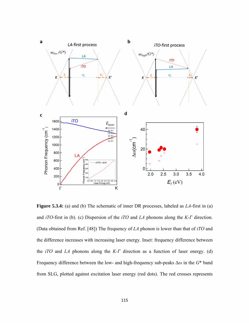
115
Figure 5.3.4: (a) and (b) The schematic of inner DR processes, labeled as LA-first in (a)
and iTO-first in (b). (c) Dispersion of the iTO and LA phonons along the K- direction.
(Data obtained from Ref. [48]) The frequency of LA phonon is lower than that of iTO and
the difference increases with increasing laser energy. Inset: frequency difference between
the iTO and LA phonons along the K- direction as a function of laser energy. (d)
Frequency difference between the low- and high-frequency sub-peaks Δω in the G* band
from SLG, plotted against excitation laser energy (red dots). The red crosses represents

116
theoretical calculated Δω for each laser energy using Eq. 5.3 and graphene phonon
dispersion relation from Ref. [48].
In Fig. 5.3.4a, the electron is first scattered (step (ii)) by an LA phonon resulting in
an electronic momentum vector / . This corresponds to a LA phonon
wave vector:
′ . (5.1)
Where is the vector connecting K and K’ points and is the momentum for the
excited electron. Similarly, the iTO phonon wave vector in Fig. 5.3.4b will be:
′ . (5.2)
Thus, the scattering by the second phonon (step (iii)) by iTO (in Fig. 5.3.4a) and
LA (in Fig. 5.3.4b) results in a Raman peak arising from phonons with the following wave
vectors: LA( )+iTO( ) or iTOLA( ) in LA-first process (Fig. 5.3.4a) and
iTO( )+LA( ) or iTOLA( ) in the iTO-first process (Fig. 5.3.4b). From Figs. 5.3.4a and
5.3.4b, ′ > ′ because the LA phonon frequency near the K point is always lower
than that of the iTO phonon (Fig. 5.3.4c). Therefore, | | > | | suggesting that the Raman
peak for iTO-first process (i.e., iTOLA( ))) corresponds higher frequency than LA-first
process (i.e., iTOLA( )). Based on this, we assign the lower and higher frequency sub-
peaks in the G* band to time-ordered LA-first and iTO-first processes, respectively.

117
Below we provide three strong evidences that support time-ordered processes as
the origin for the observed asymmetry in the G* band. Firstly, we observe that the frequency
difference (Δω) between the higher and lower frequency sub-peaks increases with El (Fig.
5.3.4d). Considering that the inner/outer processes cannot be used to rationalize the
difference between lower and higher frequency sub-peaks (see discussion regarding Fig.
5.3.2b), the observed monotonic increase of Δω as a function of El could be explained
using the time-ordered approach. In this picture, Δω = iTOLA( ) - iTOLA( ) increases
as a consequence of the increase in the difference between | | and | | (see Figs. 5.3.4a
and 5.3.4b) with El. By combining the Eqs. 5.1 and 5.2 derived above, it can be seen that
| | | | / . (5.3)
The difference between the energies of iTO and LA branches clearly diverges in the
K-Γ direction, which is reflected in the El dependence of Δω. We used Eq. 5.3 and the
phonon dispersion relation to calculated theoretical values of Δω at each laser energy, and
see a similar increasing trend as our experimental data (Fig. 5.3.4d).
5.4. Dependence of G*-bands on defects and temperature
A second evidence for the above discussed time-ordered processes involves
defects. Since our time-ordered approach involves the iTO phonon (through the iTOLA
mode), it should therefore be possible to differentiate between LA-first and iTO-first

118
processes by examining the influence of defects on the lineshape of the G* band. The
Raman scattering cross-section (Q) for a two-phonon process may be expressed as follows:
∑ , , . (5.4)
In Eq. 5.4, Mxy (x, y= a, b, and c) is the matrix element for scattering over the
intermediate states x and y, El and El - ω are the energies of the incoming and outgoing
photon, Epi (p=a, b, and c) is difference in the energy of electronic level p and the initial
level i, and γ is the broadening parameter of the electronic transition between p and i. All
the Raman scattering processes are inhomogeneously broadened by the parameter γ, which
is inversely proportional to the electron-phonon (denoted by a characteristic timescale tel-
ph) and electron–electron scattering (tel-el) time of the photo-excited carriers. The electron-
electron scattering rate (1/tel-el) for relaxing the hot carriers is proportional to (El-EF) 2 while
1/tel-ph varies as (El-EF), where EF is the Fermi energy. From the standpoint of equation 4,
the presence of a defect in the graphene lattice is expected to result in two important
changes: i) an increase in the parameter γ through the introduction of new electron-defect
scattering mechanisms, leading to the broadening of the sub-peaks in the G* band, and ii)
a decrease in the probability of two-phonon scattering processes due to the emergence of
electron-defect scattering. An increase in the probability of an electron being scattered from
one energy state to another by a defect (for example the D band process) rather than a
phonon decreases the probability of electron being scattered by phonons alone (second
order combination modes) at any fixed excitation energy and incident intensity. The

119
implications of the above points should be manifested in significant changes in the
intensities of the G* band sub-peaks in SLG with varying defect densities.
Figure 5.4.1: Plot of the intensity (normalized to the G band intensity) of the high-
frequency sub-peak and the low-frequency sub peak in the G* band against ID/IG ratios for
several CVD-grown and mechanically exfoliated SLG samples. The dotted line is a general
guide to the eye. The inset shows that the intensity ratio of the high-frequency to low-
frequency sub-peaks decreases with increasing defects due to the presence of additional
defect-scattering mechanisms.

120
Figure 5.4.1 illustrates the changes in the G* band sub-peak intensities with
varying defect density in SLG. We plot the intensities of the two sub-peaks within the G*
band against the ID/IG ratios from several CVD-grown and mechanically exfoliated SLG
samples. Note that the defects in these graphene samples were not created intentionally.
They occurred naturally during the exfoliation or CVD growth process. It can be seen
clearly from Fig. 4 that the intensity of both sub-peaks decreases markedly with increasing
defect density for SLG, as expected. This obvious decrease in intensity of the G* band
clearly validates our assertion that the addition of defects to the graphene lattice lowers the
probability of the iTO scattering process owing to an increase in the probability of
scattering by the defect. We also see that the higher frequency sub-peak (iTO-first process)
exhibits a steeper drop in intensity with increasing ID/IG compared to the lower frequency
peak. This is shown in the inset in Fig. 4d, where the ratio of intensities between the higher
frequency to lower frequency sub-peaks clearly decreases with increasing defects. The
photo-excited carriers that are initially scattered by iTO (/LA) can achieve larger
momentum changes (and hence rapidly cool down) by scattering with defects (e.g.,
iTO+defect or defect+iTO, responsible for the D band) rather than with LA (/iTO) phonons
(iTO+LA).

121
Figure 5.4.2: (a) The intensity ratio of the high-frequency to low-frequency sub-peaks
decreases with increasing temperature. (b) Plots of the dispersion of the G* band sub-peak
frequencies against temperature for mechanically exfoliated SLG. (c) The temperature
dependence of frequency difference between the high-frequency and low-frequency G*
band sub-peaks. (d) The temperature dependence of the FWHM of G* band sub-peaks.

122
In order to further explore the origin of G* band, we collected Raman spectra of
mechanically exfoliated SLG for temperatures ranging from 25 to 250 oC (Fig. 5.4.2). The
ratio of high and lower frequency sub-peak intensities was found to decrease with
increasing temperature. From the phonon-dispersion relations of graphene, the frequency
(and hence the energy) of LA phonons is always lower than iTO phonons. Thus, the average
number of LA phonons at higher temperatures is greater than iTO phonons. This difference
in LA and iTO phonon populations, at higher temperatures, is expected to increase the
probability of the LA-first resonance process. The observed decrease in the intensity ratio
of the higher frequency (iTO-first) to the lower frequency (LA-first) sub-peaks (Fig. 5.4.2a)
supports such an assertion.
The temperature dependence of Raman-active modes could be described using
i T 0i i T , (5.5)
where 0i is the harmonic frequency of the Raman-active modes [146]. (T) is the
temperature dependent perturbation of the real of the phonon self-energy. (T) could be
expressed as
i T 1i T i
2 T , (5.6)
where i1(T) describes the contribution of thermal-expansion and i
2(T) arises from
phonon-phonon coupling. The first term in Eq. 5.6 depends mainly on material properties
such as the Gruneisen parameter and coefficient of thermal expansion rather than the type
and nature of phonon and phonon-phonon interactions. On the other hand, i2(T) arises
from higher-order anharmonic terms in the Hamilotonian and includes the coupling
between phonons.

123
We found that both sub-peaks exhibit red-shift with increasing temperature, as
shown in Fig. 5.4.2b. The lower frequency peak appears to exhibit a higher slope (~ -0.09
cm-1/K) than that of the higher frequency sub-peak (~ -0.056 cm-1/K). Interestingly, these
slopes are much higher than those for the G (~-0.015-0.03 cm-1/K) reported in the literature
[147] but are on the same scale as other two-phonon modes such as G’ (-0.08-0.09 cm-1/K)
and 2D’ bands (-0.09 cm-1/K) concurring with the fact that G* is a two-phonon process. In
other words, the anharmonic term i2(T) involving phonon-phonon interactions contributes
significantly to the thermal shifts observed in the G* band. We found that the difference
between higher and lower peaks increased with increasing temperature, which may be as
explained below. From Eqs. 5.5 and 5.6, this difference may be written as
higher T lower T d0i 2higher T 2
lower T , (5.7)
where d0i is a term representing the energy difference between the lower and higher peaks
along with the thermal expansion effects (i.e., i1(T) terms). For an optical phonon of
energy Eph, the anharmonic term involving phonon-phonon coupling is,
i2 T A B
ex1 1 C
ex2 1 , (5.8)
where x1+ x2= Eph/kBT and A, B, and C are the anharmonic coupling constants. The
exponential terms in Eq. 5.8 couples one optical phonon of energy Eph to decay into two
daughter acoustic phonons of energy E1 and E2 (Klemens process). For higher temperature
processes (Eph< kBT), the anharmonic term may be estimated as
TkEE
CEBEA
x
C
x
BAT Bi
21
12
21
2 . (5.9)

124
Based on Eqs. 5.6 and 5.9,
TkEE
ECEBECEBdTT B
llllhhhhilowerhigher
21
12120 , (5.10)
where the subscript h and l correspond to higher and lower frequency sub-peaks.
The energies of iTO phonon in the higher and lower frequency sub-peaks are
different due to the time-order process. Thus, the daughter phonons arising from the decay
of iTO phonon would have different energies for higher and lower frequency sub-peaks
leading to a linear temperature dependent term in Eq. 5.10. Fig. 5.4.2c shows the
experimental results of lowerhigher with respect to temperature, the plots can be fitted
linearly, which matches with our prediction in Eq. 5.10. A complete picture of the
difference in anharmonic terms for higher and lower peaks warrants detailed theoretical
work. Nevertheless, the simple picture described above reveals the origin of temperature
dependence and indirectly validates the time-order processes. Lastly, the width of higher
and lower frequency sub-peaks also varied differently (Fig. 5.4.2d), which could also be
attributed to the difference in i2(T) terms for higher and lower frequency sub-peaks.
Following the above discussion, the time-ordered picture can also be extended to
explain the richness of the G* band in BLG and FLG samples. For instance, the three sub-
peaks which were observed in FLG (see Fig. 5.3.1c) may be understood in terms of time-
ordered scattering processes between different sub-bands. However, it may not be possible
to readily deconvolute the individual processes due to a large number of possibilities for
interband scattering (similar to the case of G’ band)[134] and the limited resolution of the
Raman spectrometer.

125
5.5. Conclusions
In conclusion, by systematically studying several SLG and FLG samples with
varying defect densities across a wide range of laser energies, we have achieved a
comprehensive understanding of the asymmetric G* band at ~2450 cm-1 in the Raman
spectrum of graphene. This band arises from a combination of iTO and LA phonons around
the K point and along the K- direction of the graphene Brillouin zone. In SLG, the G*
band can be deconvoluted into two peaks with the lower frequency (/higher frequency)
peak occurring from LA (/iTO)-first DR process. The asymmetry of the G* band is strongly
influenced by layer stacking, and at least three sub-peaks are necessary to explain the
structure of the G* band in FLG. The time-ordered scattering processes have been
supported by three strong experiment observations: i) The sub-peaks diverges with
increasing laser energy. ii) The increase in defect density in graphene was found to result
in the disappearance of the higher frequency components of the G* band. iii) The intensity
ratio of the higher frequency to the lower frequency sub-peaks decreases with temperature.

126
CHAPTER 6
SUMMARY AND FUTURE WORK
Defects are often perceived as performance limiters. Contrary to this notion, this
thesis demonstrates that defects in graphene, a one atom thick allotrope of carbon, can be
used to elicit enhanced material‘s performance, beyond predicted limits. Defects are
inevitable and entropically present which stabilize nanomaterials such as graphene. My
research found that the defect configuration and its local environment, rather than amount
of defects present in graphene, are critical for: i) overcoming fundamental limitations posed
by the so-called quantum capacitance and opening new channels for ion diffusion, ii)
inducing ferromagnetism in graphene to enable future spintronic devices, and iii) gaining
insights into fundamental time-ordered carrier scattering processes. In addition to these
fundamental discoveries at the nanoscale, my work also led to the realization of flexible
pouch supercapacitors based on defect-engineered graphene with energy densities of 500%
higher than the state-of-the-art.
In Chapter 3, we demonstrated the use of defects to improve accessibilty of the
interlayer spaces present in graphene, which alleviated the quantum capacitance bottleneck
and led to a new paradigm in energy storage. The specific capacitance of graphene
supercapacitor electrodes proved more sensitive to the defect configuration rather than
defect concentration, where defect was either in the form of pores or the nitrogen dopants.
It will be interesting to explore the effects of other dopants (e.g., B, S, O) and the presence

127
of functional groups (e.g., SiOC) in graphene on its energy storage capacity in Li-ion
batteries, Li-air batteries, etc.
In Chapter 4, we elucidated that defects and S-dopants in graphene are responsible
for the observed magnetization in graphene, which decreased upon sulfur doping
suggesting that S-dopants demagnetized vacancies and edges. Also, our density functional
theory calculations provided evidence for a net magnetization in graphene arising from its
zig-zag edges, suggesting that the contradictory conclusions on graphene magnetism
reported in the literature may stem from the magnetic properties due to different defect-
types. Interestingly, we observed peculiar local maxima in the temperature dependent
magnetizations that suggest the coexistence of different magnetic phases within the same
graphene samples. A deeper study is needed in the future to unravel the role of dopant
configuration on the magnetism, or superconductivity, in carbon nanomaterials.
In Chapter 5, we used a time-ordered scattering model to explain the origin of G*-
band ~ 2450 cm-1 in the Raman spectrum of graphene. The intensity of the G*-band has
shown to be sensitive to the concentration of defects. In addition to the G*-band, there are
also other combination Raman modes of graphene. It will be of great interest to understand
the dependence of these combination modes on the defects concentration, configuration,
and the edge states.

128
APPENDIX
Glossary of acronyms used in this dissertation
1. 2D: Two-dimensional
2. CNT: Carbon nanotube
3. SLG: Single-layer graphene
4. BLG: Bi-layer graphene
5. FLG: Few layered graphene
6. BZ: Brillouin zone
7. CVD: Chemical vapor deposition
8. EDLC: Electrical double layer capacitor
9. DOS: Density of states
10. QC: Quantum capacitance
11. CV: Cyclic voltammetry
12. HOMO: Highest occupied molecular orbitals
13. LUMO: Lowest unoccupied molecular orbitals
14. ESR: Equivalent series resistance
15. EIS: Electrochemical impedance spectroscopy
16. LA: Longitudinal acoustic
17. iTA: In-plane transverse acoustic
18. oTA: Out-of-plane transverse acoustic
19. LO: Longitudinal optic
20. iTO: In-plane transverse optic
21. oTO: Out-of-plane transverse optic
22. DR: Double-resonance
23. SC: Supercapacitor
24. DFT: Density function theory
25. GF: Graphene foam

129
26. XPS: X-ray photoelectron spectroscopy
27. SEM: Scanning electron microscopy
28. TEM: Tunneling electron microscopy
29. TEABF4: Tetraethylammonium tetrafluoroborate
30. TBAPF6: Tetrabutylammonium hexafluorophosphate
31. ACN: Acetonitrile
32. TEA+: Tetraethylammonium
33. TBA+: Tetrabutylammonium
34. PGF: Plasma etched graphene foam
35. NGF: N-doped graphene foam
36. FM: Ferromagnetic
37. GnP: Graphene nanoplatelets
38. NMP: N-Methylpyrrolidone
39. VSM: Vibrating sample magnetometer
40. SQUID: Superconducting quantum interference device
41. ZFC: Zero-field-cooled
42. FC: Field-cooled
43. ICP-MS: Inductively coupled plasma mass spectrometry
44. AFM: Atomic force microscopy

130
REFERENCES
[1] D. R. Cooper, B. D’Anjou, N. Ghattamaneni, B. Harack, M. Hilke, A. Horth, N. Majlis, M. Massicotte, L. Vandsburger, et al., “Experimental Review of Graphene,” ISRN Condens. Matter Phys. 2012, 1–56 (2012).
[2] H. X. Wang, Q. Wang, K. G. Zhou, and H. L. Zhang, “Graphene in light: Design, synthesis and applications of photo-active graphene and graphene-like materials,” Small 9, 1266–1283 (2013).
[3] F. Banhart, J. Kotakoski, and A. V. Krasheninnikov, “Structural defects in graphene,” ACS Nano 5, 26–41 (2011).
[4] A. Hashimoto, K. Suenaga, A. Gloter, K. Urita, and S. Iijima, “Direct evidence for atomic defects in graphene layers,” Nature 430, 870–873 (Nature Publishing Group, 2004).
[5] L. Tapasztó, G. Dobrik, P. Nemes-Incze, G. Vertesy, P. Lambin, and L. P. Biró, “Tuning the electronic structure of graphene by ion irradiation,” Phys. Rev. B 78, 233407 (American Physical Society, 2008).
[6] B. Anand, M. Karakaya, G. Prakash, S. S. Sankara Sai, R. Philip, P. Ayala, A. Srivastava, A. K. Sood, A. M. Rao, et al., “Dopant-configuration controlled carrier scattering in graphene,” RSC Adv. 5, 59556–59563 (The Royal Society of Chemistry, 2015).
[7] N. Ketabi, T. de Boer, M. Karakaya, J. Zhu, R. Podila, A. M. Rao, E. Z. Kurmaev, and A. Moewes, “Tuning the electronic structure of graphene through nitrogen doping: experiment and theory,” RSC Adv. 6, 56721–56727 (Royal Society of Chemistry, 2016).
[8] J. Tuček, P. Błoński, Z. Sofer, P. Šimek, M. Petr, M. Pumera, M. Otyepka, and R. Zbořil, “Sulfur Doping Induces Strong Ferromagnetic Ordering in Graphene: Effect of Concentration and Substitution Mechanism,” Adv. Mater. 28, 5045–5053 (2016).
[9] R. R. Nair, M. Sepioni, I.-L. Tsai, O. Lehtinen, J. Keinonen, A. V. Krasheninnikov, T. Thomson, A. K. Geim, and I. V. Grigorieva, “Spin-half paramagnetism in graphene induced by point defects,” Nat. Phys. 8, 199–202 (Nature Publishing Group, 2012).
[10] R. Podila, J. Chacón-Torres, J. T. Spear, T. Pichler, P. Ayala, and a. M. Rao, “Spectroscopic investigation of nitrogen doped graphene,” Appl. Phys. Lett. 101, 123108 (2012).
[11] H. Wang, T. Maiyalagan, and X. Wang, “Review on Recent Progress in Nitrogen-Doped Graphene: Synthesis, Characterization, and Its Potential Applications,” ACS Catal. 2, 781–794 (American Chemical Society, 2012).
[12] Y. Hernandez, V. Nicolosi, M. Lotya, F. M. Blighe, Z. Sun, S. De, I. T. McGovern,

131
B. Holland, M. Byrne, et al., “High-yield production of graphene by liquid-phase exfoliation of graphite,” Nat. Nanotechnol. 3, 563–568 (Nature Publishing Group, 2008).
[13] K. S. Subrahmanyam, L. S. Panchakarla, A. Govindaraj, and C. N. R. Rao, “Simple Method of Preparing Graphene Flakes by an Arc-Discharge Method,” J. Phys. Chem. C 113, 4257–4259 ( American Chemical Society, 2009).
[14] S. Stankovich, D. A. Dikin, R. D. Piner, K. A. Kohlhaas, A. Kleinhammes, Y. Jia, Y. Wu, S. T. Nguyen, and R. S. Ruoff, “Synthesis of graphene-based nanosheets via chemical reduction of exfoliated graphite oxide,” Carbon N. Y. 45, 1558–1565 (2007).
[15] K. S. Kim, Y. Zhao, H. Jang, S. Y. Lee, J. M. Kim, K. S. Kim, J.-H. Ahn, P. Kim, J.-Y. Choi, et al., “Large-scale pattern growth of graphene films for stretchable transparent electrodes,” Nature 457, 706–710 (Nature Publishing Group, 2009).
[16] P. W. Sutter, J.-I. Flege, and E. A. Sutter, “Epitaxial graphene on ruthenium,” Nat. Mater. 7, 406–411 (Nature Publishing Group, 2008).
[17] X. Li, W. Cai, J. An, S. Kim, J. Nah, D. Yang, R. Piner, A. Velamakanni, I. Jung, et al., “Large-area synthesis of high-quality and uniform graphene films on copper foils.,” Science 324, 1312–1314 (American Association for the Advancement of Science, 2009).
[18] L. Baraton, Z. B. He, C. S. Lee, C. S. Cojocaru, M. Châtelet, J.-L. Maurice, Y. H. Lee, and D. Pribat, “On the mechanisms of precipitation of graphene on nickel thin films,” EPL (Europhysics Lett. 96, 46003 (2011).
[19] G. A. López and E. J. Mittemeijer, “The solubility of C in solid Cu,” Scr. Mater. 51, 1–5 (2004).
[20] M. Winter and R. J. Brodd, “What are batteries, fuel cells, and supercapacitors?,” Chem. Rev. 104, 4245–4269 (2004).
[21] K. Kierzek, E. Frackowiak, G. Lota, G. Gryglewicz, and J. Machnikowski, “Electrochemical capacitors based on highly porous carbons prepared by KOH activation,” Electrochim. Acta 49, 515–523 (2004).
[22] E. Raymundo-Piñero, K. Kierzek, J. Machnikowski, and F. Béguin, “Relationship between the nanoporous texture of activated carbons and their capacitance properties in different electrolytes,” Carbon N. Y. 44, 2498–2507 (2006).
[23] E. Raymundo-Piñero, F. Leroux, and F. Béguin, “A High-Performance Carbon for Supercapacitors Obtained by Carbonization of a Seaweed Biopolymer,” Adv. Mater. 18, 1877–1882 (2006).
[24] L. L. Zhang, R. Zhou, and X. S. Zhao, “Graphene-based materials as supercapacitor electrodes,” J. Mater. Chem. 20, 5983 (The Royal Society of Chemistry, 2010).
[25] E. Frackowiak and F. Béguin, “Carbon materials for the electrochemical storage of

132
energy in capacitors,” Carbon N. Y. 39, 937–950 (2001).
[26] A. K. Geim and K. S. Novoselov, “The rise of graphene.,” Nat. Mater. 6, 183–191 (2007).
[27] S. Luryi, “Quantum capacitance devices,” Appl. Phys. Lett. 52, 501 (AIP Publishing, 1988).
[28] A. J. Bard and L. R. Faulkner, Electrochemical methods : fundamentals and applications, 2nd ed. (Wiley, 2001).
[29] G. A. Mabbott, “An introduction to cyclic voltammetry,” J. Chem. Educ. 60, 697–702 (1983).
[30] R. K. Emmett, M. Karakaya, R. Podila, M. R. Arcila-Velez, J. Zhu, A. M. Rao, and M. E. Roberts, “Can Faradaic processes in residual iron catalyst help overcome intrinsic EDLC limits of carbon nanotubes?,” J. Phys. Chem. C 118, 26498–26503 (2014).
[31] Y. Yang, B. Wang, J. Zhu, J. Zhou, Z. Xu, L. Fan, J. Zhu, R. Podila, A. M. Rao, et al., “Bacteria Absorption-Based Mn 2 P 2 O 7 –Carbon@Reduced Graphene Oxides for High-Performance Lithium-Ion Battery Anodes,” ACS Nano, acsnano.6b02036 (2016).
[32] S. S. K. Mallineni, J. Shannahan, A. J. Raghavendra, A. M. Rao, J. M. Brown, and R. Podila, “Biomolecular Interactions and Biological Responses of Emerging Two-Dimensional Materials and Aromatic Amino Acid Complexes,” ACS Appl. Mater. Interfaces 8, 16604–16611 (2016).
[33] B. Sengupta, W. E. Gregory, J. Zhu, S. Dasetty, M. Karakaya, J. M. Brown, A. M. Rao, J. K. Barrows, S. Sarupria, et al., “Influence of carbon nanomaterial defects on the formation of protein corona,” Rsc Adv. 5, 82395–82402 (Royal Society of Chemistry, 2015).
[34] S. S. Zhang, K. Xu, and T. R. Jow, “Electrochemical impedance study on the low temperature of Li-ion batteries,” Electrochim. Acta 49, 1057–1061 (2004).
[35] M. R. Arcila-Velez, J. Zhu, A. Childress, M. Karakaya, R. Podila, A. M. Rao, and M. E. Roberts, “Roll-to-roll synthesis of vertically aligned carbon nanotube electrodes for electrical double layer capacitors,” Nano Energy 8, 9–16 (Elsevier, 2014).
[36] M. Karakaya, J. Zhu, A. J. Raghavendra, R. Podila, S. G. Parler, J. P. Kaplan, and A. M. Rao, “Roll-to-roll production of spray coated N-doped carbon nanotube electrodes for supercapacitors,” Appl. Phys. Lett. 105, 2012–2016 (2014).
[37] P. Verma, P. Maire, and P. Novák, “A review of the features and analyses of the solid electrolyte interphase in Li-ion batteries,” Electrochim. Acta 55, 6332–6341 (2010).
[38] J. F. McCann and S. P. S. Badwal, “Equivalent Circuit Analysis of the Impedance

133
Response of Semiconductor/Electrolyte/Counterelectrode Cells,” J. Electrochem. Soc. 129, 551–559 (The Electrochemical Society, 1982).
[39] I. Epelboin, M. Keddam, and H. Takenouti, “Use of impedance measurements for the determination of the instant rate of metal corrosion,” J. Appl. Electrochem. 2, 71–79 (Kluwer Academic Publishers).
[40] W. J. Lorenz and F. Mansfeld, “Determination of corrosion rates by electrochemical DC and AC methods,” Corros. Sci. 21, 647–672 (Pergamon, 1981).
[41] I. Epelboin, M. Joussellin, and R. Wiart, “Impedance measurements for nickel deposition in sulfate and chloride electrolytes,” J. Electroanal. Chem. Interfacial Electrochem. 119, 61–71 (Elsevier, 1981).
[42] D. R. Franceschetti and J. R. Macdonald, “Small-Signal A-C Response Theory for Electrochromic Thin Films,” J. Electrochem. Soc. Electrochem. Sci. Technol. 129, 551–559 (1982).
[43] M. Etman, C. Koehler, and R. Parsons, “A pulse method for the study of the semiconductor-electrolyte interface,” J. Electroanal. Chem. Interfacial Electrochem. 130, 57–66 (Elsevier, 1981).
[44] A. Smekal, “Zur Quantentheorie der Dispersion,” Naturwissenschaften 11, 873–875 (Springer-Verlag, 1923).
[45] C. V. RAMAN and K. S. KRISHNAN, “The Optical Analogue of the Compton Effect,” Nature 121, 711–711 (1928).
[46] R. Rao, “Raman Spectroscopic Evidence for Anharmonic Phonon Lifetimes and Blueshifts in 1D Structures,” All Diss. 73 (2007).
[47] L. M. Malard, M. A. Pimenta, G. Dresselhaus, and M. S. Dresselhaus, “Raman spectroscopy in graphene,” Phys. Rep. 473, 51–87 (2009).
[48] M. S. Dresselhaus, A. Jorio, and R. Saito, “Characterizing Graphene, Graphite, and Carbon Nanotubes by Raman Spectroscopy,” Annu. Rev. Condens. Matter Phys. 1, 89–108 (2010).
[49] M. S. Dresselhaus, G. Dresselhaus, R. Saito, and A. Jorio, “Raman spectroscopy of carbon nanotubes,” Phys. Rep. 409, 47–99 (2005).
[50] M. S. Dresselhaus, G. Dresselhaus, A. Jorio, A. G. Souza Filho, and R. Saito, “Raman spectroscopy on isolated single wall carbon nanotubes,” Carbon N. Y. 40, 2043–2061 (2002).
[51] L. G. Cançado, K. Takai, T. Enoki, M. Endo, Y. A. Kim, H. Mizusaki, A. Jorio, L. N. Coelho, R. Magalhães-Paniago, et al., “General equation for the determination of the crystallite size L[sub a] of nanographite by Raman spectroscopy,” Appl. Phys. Lett. 88, 163106 (AIP Publishing, 2006).
[52] R. Rao, R. Podila, R. Tsuchikawa, J. Katoch, D. Tishler, A. M. Rao, and M. Ishigami, “Effects of layer stacking on the combination Raman modes in graphene.,”

134
ACS Nano 5, 1594–1599 (American Chemical Society, 2011).
[53] R. Saito, A. Jorio, A. G. Souza Filho, G. Dresselhaus, M. S. Dresselhaus, and M. A. Pimenta, “Probing Phonon Dispersion Relations of Graphite by Double Resonance Raman Scattering,” Phys. Rev. Lett. 88, 27401 (American Physical Society, 2001).
[54] P. Tan, C. Hu, J. Dong, W. Shen, and B. Zhang, “Polarization properties, high-order Raman spectra, and frequency asymmetry between Stokes and anti-Stokes scattering of Raman modes in a graphite whisker,” Phys. Rev. B 64, 214301 (American Physical Society, 2001).
[55] C. Liu, Z. Yu, D. Neff, A. Zhamu, and B. Z. Jang, “Graphene-Based Supercapacitor with an Ultrahigh Energy Density,” Nano Lett. 10, 4863–4868 (2010).
[56] M. D. Stoller, S. Park, Y. Zhu, J. An, and R. S. Ruoff, “Graphene-based ultracapacitors.,” Nano Lett. 8, 3498–3502 (2008).
[57] Y. Zhu, S. Murali, M. D. Stoller, K. J. Ganesh, W. Cai, P. J. Ferreira, A. Pirkle, R. M. Wallace, K. A. Cychosz, et al., “Carbon-Based Supercapacitors Produced by Activation of Graphene,” Science (80-. ). 332, 1537–1541 (2011).
[58] Y. Wang, Z. Shi, Y. Huang, Y. Ma, C. Wang, M. Chen, and Y. Chen, “Supercapacitor Devices Based on Graphene Materials,” J. Phys. Chem. C 113, 13103–13107 (American Chemical Society, 2009).
[59] R. Narayanan, H. Yamada, M. Karakaya, R. Podila, A. M. Rao, and P. R. Bandaru, “Modulation of the Electrostatic and Quantum Capacitances of Few Layered Graphenes through Plasma Processing.,” Nano Lett. 15, 3067–3072 (2015).
[60] H. Yamada and P. R. Bandaru, “Limits to the magnitude of capacitance in carbon nanotube array electrode based electrochemical capacitors,” Appl. Phys. Lett. 102, 1–5 (2013).
[61] L. L. Zhang, X. Zhao, H. Ji, M. D. Stoller, L. Lai, S. Murali, S. Mcdonnell, B. Cleveger, R. M. Wallace, et al., “Nitrogen doping of graphene and its effect on quantum capacitance, and a new insight on the enhanced capacitance of N-doped carbon,” Energy Environ. Sci. 5, 9618 (2012).
[62] B. Anand, M. Karakaya, G. Prakash, S. S. Sankara Sai, R. Philip, P. Ayala, A. Srivastava, A. K. Sood, A. M. Rao, et al., “Dopant-configuration controlled carrier scattering in graphene,” RSC Adv. 5, 59556–59563 (Royal Society of Chemistry, 2015).
[63] S. Radic, N. K. Geitner, R. Podila, A. Käkinen, P. Chen, P. C. Ke, and F. Ding, “Competitive Binding of Natural Amphiphiles with Graphene Derivatives,” Sci. Rep. 3, 2273 (Macmillan Publishers Limited. All rights reserved, 2013).
[64] B. Anand, M. Karakaya, G. Prakash, S. S. Sankara Sai, R. Philip, P. Ayala, A. Srivastava, A. K. Sood, A. M. Rao, et al., “Dopant-configuration controlled carrier scattering in graphene,” RSC Adv. 5, 59556–59563 (Royal Society of Chemistry, 2015).

135
[65] Y. Shim and H. J. Kim, “Nanoporous Carbon Supercapacitors in an Ionic Liquid: A Computer Simulation Study,” ACS Nano 4, 2345–2355 (American Chemical Society, 2010).
[66] P. Wu, J. Huang, V. Meunier, B. G. Sumpter, and R. Qiao, “Complex Capacitance Scaling in Ionic Liquids-Filled Nanopores,” ACS Nano 5, 9044–9051 (American Chemical Society, 2011).
[67] G. Feng and P. T. Cummings, “Supercapacitor capacitance exhibits oscillatory behavior as a function of nanopore size,” J. Phys. Chem. Lett. 2, 2859–2864 (2011).
[68] C. Largeot, C. Portet, J. Chmiola, P. L. Taberna, Y. Gogotsi, and P. Simon, “Relation between the ion size and pore size for an electric double-layer capacitor,” J. Am. Chem. Soc. 130, 2730–2731 (2008).
[69] C. Merlet, C. Péan, B. Rotenberg, P. a Madden, B. Daffos, P.-L. Taberna, P. Simon, and M. Salanne, “Highly confined ions store charge more efficiently in supercapacitors.,” Nat. Commun. 4, 2701 (2013).
[70] P. Simon and Y. Gogotsi, “Materials for electrochemical capacitors.,” Nat. Mater. 7, 845–854 (2008).
[71] J. Chmiola, G. Yushin, Y. Gogotsi, C. Portet, P. Simon, and P. L. Taberna, “Anomalous Increase in Carbon Capacitance at Pore Sizes Less Than 1 Nanometer,” Science (80-. ). 313, 1760–1763 (2006).
[72] L. Xing, J. Vatamanu, O. Borodin, and D. Bedrov, “On the atomistic nature of capacitance enhancement generated by ionic liquid electrolyte confined in subnanometer pores,” J. Phys. Chem. Lett. 4, 132–140 (2013).
[73] L. Liu, X. Yue, J. Zhao, Q. Cheng, and J. Tang, “Graphene antidot lattices as potential electrode materials for supercapacitors,” Phys. E Low-dimensional Syst. Nanostructures 69, 316–321 (2015).
[74] L. G. Cançado, A. Jorio, E. H. M. Ferreira, F. Stavale, C. A. Achete, R. B. Capaz, M. V. O. Moutinho, A. Lombardo, T. S. Kulmala, et al., “Quantifying defects in graphene via Raman spectroscopy at different excitation energies.,” Nano Lett. 11, 3190–3196 (American Chemical Society, 2011).
[75] L. G. Cançado, K. Takai, T. Enoki, M. Endo, Y. A. Kim, H. Mizusaki, A. Jorio, L. N. Coelho, R. Magalhães-Paniago, et al., “General equation for the determination of the crystallite size L[sub a] of nanographite by Raman spectroscopy,” Appl. Phys. Lett. 88, 163106 (AIP Publishing, 2006).
[76] G. Luo, L. Liu, J. Zhang, G. Li, B. Wang, and J. Zhao, “Hole defects and nitrogen doping in graphene: implication for supercapacitor applications.,” ACS Appl. Mater. Interfaces 5, 11184–11193 (American Chemical Society, 2013).
[77] J. Gamby, P. L. Taberna, P. Simon, J. F. Fauvarque, and M. Chesneau, “Studies and characterisations of various activated carbons used for carbon/carbon supercapacitors,” J. Power Sources 101, 109–116 (2001).

136
[78] Z. Jiang, Z. Jiang, X. Tian, and W. Chen, “Amine-functionalized holey graphene as a highly active metal-free catalyst for the oxygen reduction reaction,” J. Mater. Chem. A 2, 441–450 (2014).
[79] M. M. Sk and C. Y. Yue, “Layer-by-layer (LBL) assembly of graphene with p-phenylenediamine (PPD) spacer for high performance supercapacitor applications,” RSC Adv. 4, 19908–19915 (2014).
[80] K. Zhang, L. L. Zhang, X. S. Zhao, and J. Wu, “Graphene/Polyaniline Nanofiber Composites as Supercapacitor Electrodes,” Chem. Mater. 22, 1392–1401 (2010).
[81] D. Yu, K. Goh, H. Wang, L. Wei, W. Jiang, Q. Zhang, L. Dai, and Y. Chen, “Scalable synthesis of hierarchically structured carbon nanotube-graphene fibres for capacitive energy storage,” Nat Nano 9, 555–562 (Nature Publishing Group, 2014).
[82] J. J. Yoo, K. Balakrishnan, J. Huang, V. Meunier, B. G. Sumpter, A. Srivastava, M. Conway, A. L. M. Reddy, J. Yu, et al., “Ultrathin planar graphene supercapacitors.,” Nano Lett. 11, 1423–1427 (2011).
[83] Z. Wu, K. Parvez, X. Feng, and K. Müllen, “Graphene-based in-plane micro-supercapacitors with high power and energy densities,” Nat Commun 4 (Nature Publishing Group, a division of Macmillan Publishers Limited. All Rights Reserved., 2013).
[84] H. Y. Jung, M. B. Karimi, M. G. Hahm, P. M. Ajayan, and Y. J. Jung, “Transparent, flexible supercapacitors from nano-engineered carbon films.,” Sci. Rep. 2, 773 (Nature Publishing Group, 2012).
[85] Z. Chen, W. Ren, L. Gao, B. Liu, S. Pei, and H.-M. Cheng, “Three-dimensional flexible and conductive interconnected graphene networks grown by chemical vapour deposition.,” Nat. Mater. 10, 424–428 (Nature Publishing Group, 2011).
[86] M. J. Allen, V. C. Tung, and R. B. Kaner, “Honeycomb carbon: A review of graphene,” Chem. Rev. 110, 132–145 (2010).
[87] Z. H. Ni, L. a. Ponomarenko, R. R. Nair, R. Yang, S. Anissimova, I. V. Grigorieva, F. Schedin, P. Blake, Z. X. Shen, et al., “On resonant scatterers as a factor limiting carrier mobility in graphene,” Nano Lett. 10, 3868–3872 (2010).
[88] C. R. Dean, a F. Young, I. Meric, C. Lee, L. Wang, S. Sorgenfrei, K. Watanabe, T. Taniguchi, P. Kim, et al., “Boron nitride substrates for high-quality graphene electronics.,” Nat. Nanotechnol. 5, 722–726 (Nature Publishing Group, 2010).
[89] L. E. Hueso, J. M. Pruneda, V. Ferrari, G. Burnell, J. P. Valdés-Herrera, B. D. Simons, P. B. Littlewood, E. Artacho, A. Fert, et al., “Transformation of spin information into large electrical signals using carbon nanotubes.,” Nature 445, 410–413 (2007).
[90] K. Tsukagoshi, B. W. Alphenaar, and H. Ago, “Coherent transport of electron spin in a ferromagnetically contacted carbon nanotube,” 572–574 (1999).

137
[91] J. W. McClure, “Diamagnetism of Graphite,” Phys. Rev. 104, 666–671 (American Physical Society, 1956).
[92] P. Esquinazi, A. Setzer, R. Höhne, C. Semmelhack, Y. Kopelevich, D. Spemann, T. Butz, B. Kohlstrunk, and M. Lösche, “Ferromagnetism in oriented graphite samples,” Phys. Rev. B 66, 24429 (American Physical Society, 2002).
[93] P. O. Lehtinen, A. S. Foster, Y. Ma, A. V Krasheninnikov, and R. M. Nieminen, “Irradiation-induced magnetism in graphite: a density functional study.,” Phys. Rev. Lett. 93, 187202 (American Physical Society, 2004).
[94] O. V Yazyev, “Magnetism in disordered graphene and irradiated graphite.,” Phys. Rev. Lett. 101, 37203 (American Physical Society, 2008).
[95] K. Sawada, F. Ishii, M. Saito, S. Okada, and T. Kawai, “Phase control of graphene nanoribbon by carrier doping: appearance of noncollinear magnetism.,” Nano Lett. 9, 269–272 (American Chemical Society, 2009).
[96] K. Wakabayashi, M. Fujita, H. Ajiki, and M. Sigrist, “Electronic and magnetic properties of nanographite ribbons,” Phys. Rev. B 59, 8271–8282 (American Physical Society, 1999).
[97] K. Kusakabe and M. Maruyama, “Magnetic nanographite,” Phys. Rev. B 67, 92406 (American Physical Society, 2003).
[98] T. L. Makarova, B. Sundqvist, R. Höhne, P. Esquinazi, Y. Kopelevich, P. Scharff, V. A. Davydov, L. S. Kashevarova, and A. V Rakhmanina, “Magnetic carbon.,” Nature 413, 716–718 (2001).
[99] A. V. Rode, E. G. Gamaly, A. G. Christy, J. G. Fitz Gerald, S. T. Hyde, R. G. Elliman, B. Luther-Davies, A. I. Veinger, J. Androulakis, et al., “Unconventional magnetism in all-carbon nanofoam,” Phys. Rev. B 70, 54407 (American Physical Society, 2004).
[100] H. Ohldag, T. Tyliszczak, R. Höhne, D. Spemann, P. Esquinazi, M. Ungureanu, and T. Butz, “pi-electron ferromagnetism in metal-free carbon probed by soft x-ray dichroism.,” Phys. Rev. Lett. 98, 187204 (American Physical Society, 2007).
[101] A. H. Castro Neto, N. M. R. Peres, K. S. Novoselov, and A. K. Geim, “The electronic properties of graphene,” Rev. Mod. Phys. 81, 109–162 (American Physical Society, 2009).
[102] D. Soriano, F. Muñoz-Rojas, J. Fernández-Rossier, and J. J. Palacios, “Hydrogenated graphene nanoribbons for spintronics,” Phys. Rev. B 81, 165409 (American Physical Society, 2010).
[103] F. J. Culchac, A. Latgé, and A. T. Costa, “Spin waves in zigzag graphene nanoribbons and the stability of edge ferromagnetism,” New J. Phys. 13, 33028 (IOP Publishing, 2011).
[104] H. Feldner, Z. Y. Meng, T. C. Lang, F. F. Assaad, S. Wessel, and A. Honecker,

138
“Dynamical signatures of edge-state magnetism on graphene nanoribbons.,” Phys. Rev. Lett. 106, 226401 (American Physical Society, 2011).
[105] Y.-W. Son, M. L. Cohen, and S. G. Louie, “Half-metallic graphene nanoribbons.,” Nature 444, 347–349 (2006).
[106] O. V Yazyev, “Emergence of magnetism in graphene materials and nanostructures,” Reports Prog. Phys. 73, 56501 (IOP Publishing, 2010).
[107] M. Sepioni, R. R. Nair, S. Rablen, J. Narayanan, F. Tuna, R. Winpenny, A. K. Geim, and I. V Grigorieva, “Limits on intrinsic magnetism in graphene.,” Phys. Rev. Lett. 105, 207205 (American Physical Society, 2010).
[108] Y. Wang, Y. Huang, Y. Song, X. Zhang, Y. Ma, J. Liang, and Y. Chen, “Room-temperature ferromagnetism of graphene.,” Nano Lett. 9, 220–224 (American Chemical Society, 2009).
[109] H. S. S. R. Matte, K. S. Subrahmanyam, and C. N. R. Rao, “Novel Magnetic Properties of Graphene: Presence of Both Ferromagnetic and Antiferromagnetic Features and Other Aspects,” J. Phys. Chem. C 113, 9982–9985 (American Chemical Society, 2009).
[110] S. S. Rao, S. N. Jammalamadaka, A. Stesmans, V. V Moshchalkov, J. van Tol, D. V Kosynkin, A. Higginbotham-Duque, and J. M. Tour, “Ferromagnetism in graphene nanoribbons: split versus oxidative unzipped ribbons.,” Nano Lett. 12, 1210–1217 (American Chemical Society, 2012).
[111] R. Podila, W. Queen, A. Nath, J. T. Arantes, A. L. Schoenhalz, A. Fazzio, G. M. Dalpian, J. He, S. J. Hwu, et al., “Origin of FM ordering in pristine micro- and nanostructured ZnO.,” Nano Lett. 10, 1383–1386 (American Chemical Society, 2010).
[112] B. B. Straumal, A. A. Mazilkin, S. G. Protasova, A. A. Myatiev, P. B. Straumal, G. Schütz, P. A. van Aken, E. Goering, and B. Baretzky, “Magnetization study of nanograined pure and Mn-doped ZnO films: Formation of a ferromagnetic grain-boundary foam,” Phys. Rev. B 79, 205206 (American Physical Society, 2009).
[113] T. Tietze, P. Audehm, Y.-C. Chen, G. Schütz, B. B. Straumal, S. G. Protasova, A. A. Mazilkin, P. B. Straumal, T. Prokscha, et al., “Interfacial dominated ferromagnetism in nanograined ZnO: a μSR and DFT study.,” Sci. Rep. 5, 8871 (Nature Publishing Group, 2015).
[114] S. G. Protasova, B. B. Straumal, A. A. Mazilkin, S. V. Stakhanova, P. B. Straumal, and B. Baretzky, “Increase of Fe solubility in ZnO induced by the grain boundary adsorption,” J. Mater. Sci. 49, 4490–4498 (2014).
[115] P. E. Blöchl, “Projector augmented-wave method,” Phys. Rev. B 50, 17953–17979 (American Physical Society, 1994).
[116] G. Kresse, “From ultrasoft pseudopotentials to the projector augmented-wave method,” Phys. Rev. B 59, 1758–1775 (American Physical Society, 1999).

139
[117] G. Kresse, “Efficient iterative schemes for ab initio total-energy calculations using a plane-wave basis set,” Phys. Rev. B 54, 11169–11186 (American Physical Society, 1996).
[118] G. Kresse and J. Furthmüller, “Efficiency of ab-initio total energy calculations for metals and semiconductors using a plane-wave basis set,” Comput. Mater. Sci. 6, 15–50 (1996).
[119] J. P. Perdew, K. Burke, and M. Ernzerhof, “Generalized Gradient Approximation Made Simple,” Phys. Rev. Lett. 77, 3865–3868 (American Physical Society, 1996).
[120] E. Z. Kurmaev, A. V. Galakhov, A. Moewes, S. Moehlecke, and Y. Kopelevich, “Interlayer conduction band states in graphite-sulfur composites,” Phys. Rev. B 66, 193402 (American Physical Society, 2002).
[121] B. C. Zhao, Y. Q. Ma, W. H. Song, and Y. P. Sun, “Magnetization steps in the phase separated manganite La0.275Pr0.35Ca0.375MnO3,” Phys. Lett. A 354, 472–476 (2006).
[122] Y. Ma, P. O. Lehtinen, A. S. Foster, and R. M. Nieminen, “Magnetic properties of vacancies in graphene and single-walled carbon nanotubes,” New J. Phys. 6, 68–68 (IOP Publishing, 2004).
[123] A. A. El-Barbary, R. H. Telling, C. P. Ewels, M. I. Heggie, and P. R. Briddon, “Structure and energetics of the vacancy in graphite,” Phys. Rev. B 68, 144107 (American Physical Society, 2003).
[124] H. Park, A. Wadehra, J. W. Wilkins, and A. H. Castro Neto, “Spin-polarized electronic current induced by sublattice engineering of graphene sheets with boron/nitrogen,” Phys. Rev. B 87, 85441 (American Physical Society, 2013).
[125] H. Park, A. Wadehra, J. W. Wilkins, and A. H. Castro Neto, “Magnetic states and optical properties of single-layer carbon-doped hexagonal boron nitride,” Appl. Phys. Lett. 100, 253115 (AIP Publishing, 2012).
[126] F. Wu, E. Kan, H. Xiang, S.-H. Wei, M.-H. Whangbo, and J. Yang, “Magnetic states of zigzag graphene nanoribbons from first principles,” Appl. Phys. Lett. 94, 223105 (AIP Publishing, 2009).
[127] L. Chen, L. Guo, Z. Li, H. Zhang, J. Lin, J. Huang, S. Jin, and X. Chen, “Towards intrinsic magnetism of graphene sheets with irregular zigzag edges.,” Sci. Rep. 3, 2599 (Nature Publishing Group, 2013).
[128] S.-Q. Zhao, Y. Lü, W.-G. Lü, W.-J. Liang, and E.-G. Wang, “Modulating magnetism of nitrogen-doped zigzag graphene nanoribbons,” Chinese Phys. B 23, 67305 (IOP Publishing, 2014).
[129] R. C. Weast, Ed., CRC Handbook of Chemistry and Physics, 63rd ed. (CRC Press LLC, 1984).
[130] A. C. Ferrari and D. M. Basko, “Raman spectroscopy as a versatile tool for studying

140
the properties of graphene.,” Nat. Nanotechnol. 8, 235–246 (Nature Publishing Group, a division of Macmillan Publishers Limited. All Rights Reserved., 2013).
[131] A. Jorio, M. S. Dresselhaus, R. Saito, and G. Dresselhaus, Raman Spectroscopy in Graphene Related Systems (Wiley-VCH, 2011).
[132] R. Podila, R. Rao, R. Tsuchikawa, M. Ishigami, and A. M. Rao, “Raman spectroscopy of folded and scrolled graphene.,” ACS Nano 6, 5784–5790 (American Chemical Society, 2012).
[133] C. Thomsen and S. Reich, “Double resonant raman scattering in graphite,” Phys. Rev. Lett. 85, 5214–5217 (American Physical Society, 2000).
[134] L. M. Malard, M. A. Pimenta, G. Dresselhaus, and M. S. Dresselhaus, “Raman spectroscopy in graphene,” Phys. Rep. 473, 51–87 (2009).
[135] R. Saito, A. Jorio, A. G. Souza Filho, G. Dresselhaus, M. S. Dresselhaus, and M. A. Pimenta, “Probing phonon dispersion relations of graphite by double resonance Raman scattering.,” Phys. Rev. Lett. 88, 27401 (American Physical Society, 2002).
[136] R. J. Nemanich and S. A. Solin, “First- and second-order Raman scattering from finite-size crystals of graphite,” Phys. Rev. B 20, 392–401 (American Physical Society, 1979).
[137] P. Tan, Y. Deng, and Q. Zhao, “Temperature-dependent Raman spectra and anomalous Raman phenomenon of highly oriented pyrolytic graphite,” Phys. Rev. B 58, 5435–5439 (American Physical Society, 1998).
[138] T. Shimada, T. Sugai, C. Fantini, M. Souza, L. G. Cançado, A. Jorio, M. A. Pimenta, R. Saito, A. Grüneis, et al., “Origin of the 2450cm−1 Raman bands in HOPG, single-wall and double-wall carbon nanotubes,” Carbon N. Y. 43, 1049–1054 (2005).
[139] D. L. Mafra, G. Samsonidze, L. M. Malard, D. C. Elias, J. C. Brant, F. Plentz, E. S. Alves, and M. A. Pimenta, “Determination of LA and TO phonon dispersion relations of graphene near the Dirac point by double resonance Raman scattering,” Phys. Rev. B 76, 233407 (American Physical Society, 2007).
[140] P. T. Araujo, D. L. Mafra, K. Sato, R. Saito, J. Kong, and M. S. Dresselhaus, “Phonon self-energy corrections to nonzero wave-vector phonon modes in single-layer graphene.,” Phys. Rev. Lett. 109, 46801 (American Physical Society, 2012).
[141] P. May, M. Lazzeri, P. Venezuela, F. Herziger, G. Callsen, J. S. Reparaz, A. Hoffmann, F. Mauri, and J. Maultzsch, “Signature of the two-dimensional phonon dispersion in graphene probed by double-resonant Raman scattering,” Phys. Rev. B 87, 75402 (American Physical Society, 2013).
[142] Z. Luo, C. Cong, J. Zhang, Q. Xiong, and T. Yu, “The origin of sub-bands in the Raman D-band of graphene,” Carbon N. Y. 50, 4252–4258 (2012).
[143] X. Li, W. Cai, J. An, S. Kim, J. Nah, D. Yang, R. Piner, A. Velamakanni, I. Jung, et al., “Large-area synthesis of high-quality and uniform graphene films on copper

141
foils.,” Science 324, 1312–1314 (American Association for the Advancement of Science, 2009).
[144] D. L. Mafra, E. A. Moujaes, S. K. Doorn, H. Htoon, R. W. Nunes, and M. A. Pimenta, “A study of inner process double-resonance Raman scattering in bilayer graphene,” Carbon N. Y. 49, 1511–1515 (2011).
[145] P. Venezuela, M. Lazzeri, and F. Mauri, “Theory of double-resonant Raman spectra in graphene: Intensity and line shape of defect-induced and two-phonon bands,” Phys. Rev. B 84, 35433 (American Physical Society, 2011).
[146] H. H. Burke and I. P. Herman, “Temperature dependence of Raman scattering in Ge 1 − x Si x alloys,” Phys. Rev. B 48, 15016–15024 (American Physical Society, 1993).
[147] I. Calizo, A. A. Balandin, W. Bao, F. Miao, and C. N. Lau, “Temperature Dependence of the Raman Spectra of Graphene and Graphene Multilayers,” Nano Lett. 7, 2645–2649 (2007).
Related Documents