An Analysis of the Fundamental Constraints on Low Cost Passive Radio-Frequency Identification System Design by Tom Ahlkvist Scharfeld B.S., Mechanical Engineering (1998) Northwestern University Submitted to the Department of Mechanical Engineering In Partial Fulfillment of the Requirements for the Degree of Master of Science at the Massachusetts Institute of Technology August 2001 © 2001 Massachusetts Institute of Technology All rights reserved MASSACHUSMiTS INSTITUTE OF TECHNOLOGY DEC 1 02001 LIBRARIES iAdROhwvL Signature of Author. ........................... ..................... ...... .... ...... Department of Mechanical Engin&r ing August 21, 2001 C ertified by .................................................................... / ............. u...... ..................................... Sanjay E. Sarma Associate Professor of Mechanical Engineering Thesis Supervisor A ccepted by .... .................................................................... .,. ........................................ Ain A. Sonin Chairman, Department Committee on Graduate Students

Welcome message from author
This document is posted to help you gain knowledge. Please leave a comment to let me know what you think about it! Share it to your friends and learn new things together.
Transcript
/
An Analysis of the Fundamental Constraints onLow Cost Passive Radio-Frequency Identification System Design
by
Tom Ahlkvist Scharfeld
B.S., Mechanical Engineering (1998)
Northwestern University
Submitted to the Department of Mechanical EngineeringIn Partial Fulfillment of the Requirements for the Degree of
Master of Science
at the
Massachusetts Institute of Technology
August 2001
© 2001 Massachusetts Institute of TechnologyAll rights reserved
MASSACHUSMiTS INSTITUTEOF TECHNOLOGY
DEC 1 02001
LIBRARIESiAdROhwvL
Signature of Author. ........................... ..................... ...... .... ......Department of Mechanical Engin&r ing
August 21, 2001
C ertified by .................................................................... / ............. u...... .....................................Sanjay E. Sarma
Associate Professor of Mechanical EngineeringThesis Supervisor
A ccepted by .... .................................................................... .,. ........................................Ain A. Sonin
Chairman, Department Committee on Graduate Students
An Analysis of the Fundamental Constraints onLow Cost Passive Radio Frequency Identification System Design
by
Tom Ahlkvist Scharfeld
Submitted to the Department of Mechanical EngineeringOn August 21, 2001 in partial fulfillment of the
Requirements for the Degree of Master of Science
Abstract
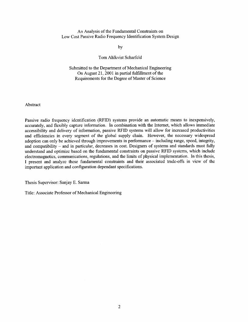
Passive radio frequency identification (RFID) systems provide an automatic means to inexpensively,accurately, and flexibly capture information. In combination with the Internet, which allows immediateaccessibility and delivery of information, passive RFID systems will allow for increased productivitiesand efficiencies in every segment of the global supply chain. However, the necessary widespreadadoption can only be achieved through improvements in performance - including range, speed, integrity,and compatibility - and in particular, decreases in cost. Designers of systems and standards must fullyunderstand and optimize based on the fundamental constraints on passive RFID systems, which includeelectromagnetics, communications, regulations, and the limits of physical implementation. In this thesis,I present and analyze these fundamental constraints and their associated trade-offs in view of theimportant application and configuration dependant specifications.
Thesis Supervisor: Sanjay E. Sarma
Title: Associate Professor of Mechanical Engineering
---- ·

ACKNOWLEDGEMENTS
When I arrived at MIT two years ago, I had little background in the material covered in this thesis. I wishto thank my advisor, Sanjay Sarma, most of all, for allowing me to move into an entirely new domain;one in which there were many better equipped at MIT. Sanjay has allowed me tremendous flexibility andfreedom in defining a topic and preparing my thesis. Over the past two years, through the multiple topics Ihave explored, I have learned a tremendous amount. I owe much of this to Sanjay. Meetings were alwaysmotivating. Though Sanjay has been, and will likely continue to be incredibly busy, he has always madehimself available for meetings, emails, and phone calls, at home or on the road.
I must also thank Dan Engels. Where Sanjay provided the freedom, Dan provided the push. Had it notbeen for Dan, I would likely have allowed myself much less time to write. Discussions with Dan werealways interesting and insightful. His extreme distaste for gates and functionality has been infectious.
I would like to thank the others at the Auto-ID Center. Kevin Ashton was very helpful in providing themuch needed and often ignored insight into the requirements of the end user community. BrookePeterson, Tracy Skeete, and David Rodriguera provided the support to make the Center an exciting,productive, and friendly place to work.
I must also thank those outside of MIT and the Auto-ID Center whose insights were invaluable. TheAlien Technology and Wave-ID team, including John Rolin, Roger Stewart, and Curt Carrender, providedthe essential practical and industrial viewpoint. Through them, not only did I learn a great deal about thetechnology, but also its development. My brief encounters with Matt Reynolds and even brieferencounters with Peter Cole were more helpful than they might imagine.
Finally, I must thank my friends for making MIT a truly enjoyable place to be, my officemates forgraciously accepting my constant presence for the last few months, my housemates for graciouslyaccepting my constant absence for the last few months, and my family for supporting me in spite of notknowing what I was doing. Special thanks to Jean Ah Lee for thoroughly reading my thesis, SteveBuerger for offering to read my thesis, my Mother, in spite of her Swedish tongue, for suggesting a fewcorrections, my Father for painstakingly lumbering through my thesis, Jenny Scharfeld for reading thefirst paragraph, and Anna Scharfeld for checking to see how long it was.
TABLE OF CONTENTS
1 INTRO DUCTION ............................................................................................................................... 8
1.1 Introduction................................. .......... ..................... 8
1.2 Brief H istory of R FID ........................... .......... ..................................... ....................... 9
1.3 Classifications of RFID Systems ........................................ ....................... 101.3.1 Chipless versus Chip......................................... ............. ............ 101.3.2 Passive, Semi-Passive, and Active.............................. ......................... 111.3.3 Read-only and Read-write ........................................ ........................ 11
1.4 Assumptions.......................... .. .............. ............. ............................. 11
1.5 Specifications .............................................. ...................... ......... ..... .................. 111.5.1 P erform an ce ................................................................................................ .................. 121.5.2 Cost and Size ................ .......................... ...................... 13
1.6 Functions, Constraints and Organization ...................................... 131.6.1 Components and their Functions............................... ............... 131.6.2 Constraints and Organization............................ .......................... 15
2 ELECTROMAGNETICS AND ANTENNAS ........................................................................ 16
2.1 Introduction.......................... ............... ............. 16
2.2 Maxwell's Equations and Electromagnetics Fundamentals............................................ 16
2.3 Antennas and Their Surrounding Regions ........................................................... 18
2.4 Impedance of Space, Antennas, and Circuits..................................................... 20
2.5 Coupling in the Near Field and Far Field ................................................ 222.5.1 Near-field Coupling ............................. ....... ......... .............. 22
2.5.1.1 Inductive Coupling......................................................... 222.5.1.1.1 Resonance and Q ..... ........................................ 252.5.1.1.2 Load Modulation ........................................ ................... 252.5.1.1.3 Voltage Available to Load....................................................... 26
2.5.1.2 Capacitive Coupling.................................................... 262.5.1.2.1 Resonance and Load Modulation ...................... ....................... 27
2.5.2 Far-field Coupling................................. ........................... 272.5.2.1 Antenna Parameters ......................................... . ....................................... 272.5.2.2 Transmission and Reception ........................................ ................. 292.5.2.3 Reader to Tag Transmission ........................................ .................. 292.5.2.4 Backscatter Modulation ........................................................... 31
2.5.2.4.1 Scattering ............... ............................... .......................... 312.5.2.4.2 Scattering and Radar Cross Section.............................. ........................ 312.5.2.4.3 Antenna Scattering................................ ............... 322.5.2.4.4 Power Scattered and Power Received ........................................ 34
2.6 Environmental Influences .......................................................... .......... ............... 342 .6 .1 L oss ......................................................................................................... .................. 35
2.6.1.1 Near-field Loss .............. ...................... .............................. 352.6.1.2 Far-field Loss and M ultipath...................................................... 35
2.6.2 Other Antennas ........................................................... 372.6.3 Temperature and Humidity ...................................... .............................. 37
2 .7 Sum m ary ................................................................................. 37
3 COM M UNICATIONS...................................................................................................................... 38
3.1 Introduction........ .............. ........................ ............... ............... 38
3.2 Com munications Process .......................................................... .......... ................... 38
3.3 Signal and Spectra Fundamentals ........................................ ................ 383.3.1 Time Averaging, Power, and RMS ................................................................ 393.3.2 Fourier and Spectra ................................................. ................. 39
3.3.2.1 Rectangular Pulse.................................... .... .............. ............ 403.3.2.2 Rectangular Pulse Train ........................................ ................... 413.3.2.3 Filtering .................................................. ......... 433.3.2.4 M odulation ................. ............................. ........................ 443.3.2.5 Bandw idth ......................................................... .......... .............. 44
3.4 L ine C oding ................................................................................................................................ 453.4.1 Baseband Power Spectral Densities ................................................ 47
3.4.1.1 NRZ..... ................................ 493.4 .1.2 R Z ............................................................................................................ ................. 4 93.4.1.3 M anchester................................ ...................................... ....................... 503.4.1.4 PW M and PPM ........................ ............... ....................... .... 513.4.1.5 Miller and FMO ................................................. 53
3.53.5.1
3.3.
3.5.23.3.
3.5.3
3.63.6.13.6.2
3.7
3.8
M odulation....................................................... ..................... 55Reader to Tag Coding and Modulation.................................... 56
5.1.1 Amplitude Shift Key (ASK) ....................................... ...................... 565.1.2 Envelope Detection ........................................................ .............. 57
Tag to Reader Modulation and Coding .................................... ............................ 585.2.1 Subcarrier ....................... ... .. ................................................ ....................... 585.2.2 C oding .......................... .................................................................... 58
Spread Spectrum .............. ................................................................. 59
Probability of Error ......................... ................ ............................. 59B urst N oise...................................... ................ ............ 60G aussian N oise.......................................... .............. ............. 60
Error Detection and Correction.................................. .................. 61
Sum m ary .................................................................... ............... 62
4 REG ULATIO N S ............................................................................................................................... 63
4.1 Introduction........... ....... ............................................... 63
4.2 Necessity of Common Allocations ..................................................................... 63
4.3 Worldwide Structure of Regulatory Organizations........................ ......................... 634.3.1 ITU ...................................................................... ............... 634.3.2 R egional/N ational ............................ ...... ............................................................ 64
4.4 Frequencies Available for RFID Use..................................... ................. 654.4.1 ISM ...................................................................... ............. 654.4.2 O ther (LF/U H F) .................................................................................................... 66
4.5 Radiation, Bandwidth, and Detection Specifications...................................... 664.5.1 Field Strength and Power Conversion .................................................... 67
4.5.1.1 Far-field .......................................... 674.5.1.2 N ear-field .................................................. 67
4.5.2 Bandw idth ................................................... 684.5.3 D etection .................................................. 68
4.6 Frequencies and Lim its ............................................................................................................... 704.6.1 N ear-field Operation Frequencies ..................................... ......................... 70
4.6.1.1 9 kH z - 135 kH z .............................................................................................................. 704.6.1.2 6.78 M H z .................................................. 724.6.1.3 13.56 M H z ................................................... 724.6.1.4 27.12 M H z ................................................... 734.6.1.5 40.68 M H z ............................................ ... ....................................... ... .......... ............. 74
4.6.2 Far-field O peration Frequencies ............................................................ ....................... 744.6.2.1 433.92 M H z .......................................................... 754.6.2.2 862-870 M H z .................................................... 754.6.2.3 915 M H z ................................................... 764.6.2.4 2.45 GH z ................................................... 774.6.2.5 5.78 GH z ............................................................. ................................................. 79
4.7 Sum m ary .......................................................................................................................... 79
5 PHYSICAL IMPLEMENTATION ................................................................................................. 81
5.1 Introduction........................................ 81
5.2 Antennas ..................................................................................................................................... 815.2.1 N ear-field ............................................................................................................................ 825.2.2 Far-field ............................................ 83
5.2.2.1 D ipole A ntennas.............................................................................................................. 845.2.2.2 M icrostrip Patch A ntennas.......................................... .............................................. 84
5.3 Integrated Circuit .................................................. 855.3.1 Overall Architecture............................................................................................................ 855.3.2 Components .................................................. 85
5.3.2.1 Semiconductors and Transistors ...................................................... 865.3.2.2 Passive Com ponents .................................................................... ............................. 87
5.3.2.2.1 Resistors.................................................................................................................... 875.3.2.2.2 Capacitors ................................................................................................................. 875.3.2.2.3 Inductors ................................................................................................................... 88
5.3.2.3 Charge Pum ps ................................................................................................................. 885.3.2.4 D iodes ............................................................................................................................. 885.3.2.5 O scillators .................................................... 885.3.2.6 Phase-Locked Loops .................................................. 885.3.2.7 D igital Circuits................................................................................................................ 89
5.3.2.7.1 Flip-Flops and Latches .............................................................. ......................... 895.3.2.7.2 Shift Registers........................................................................................................... 89
5.3.2.8 One-shots .................................................. 895.3.2.9 M em ory ............................................. 89
5.3.3 Integrated Circuit Pow er Consum ption.................................................................... 90
5.4 Attachm ent and Packaging.......................................................................................................... 91
5 .5 Su m m ary ..................................................................................................................................... 9 1
6 COM M AND PROTOCOLS ............................................................................................................ 92
6 .1 In trodu ction ................................................................................................................................. 92
6.2 Anti-Collision Overview............................................................... 926.2.1 Anti-Collision Analysis............................................... ......... 95
6.2.1.1 SuperTag . .... .................................... .................................. ..................... 956.2.1.2 Query-Tree Based ........................................ .............. 966.2.1.3 Results............................................. .............................. 976.2.1.4 Com parison ......................................... .................. ............ ............. 98
6.2.2 Channelization ............................. ... ............................ ............. 996.2.3 System Considerations ........................................ ......................... 99
6.3 Com m ands ................................................ ......................... 996.3.1 Commands and Bandwidth ....................................... ....................... 99
6.4 Sum m ary .......................................... .................... ..... ..................... 100
7 INFLUENCE OF CONSTRAINTS ON PERFORMANCE SPECIFICATIONS .................. 101
7.1 Introduction......................... ............... . .. .... ................ .............. ........................ 101
7.2 R ange ............................................................. ...... .. ............................. 1017.2.1 Field Strength, Orientation, and the Environment ......................................... ..... 1027.2.2 Power Reception, Delivery, and Consumption ............................................... 102
7.3 Speed and Integrity ....................................... .... .... .. . ........... ...... ............................ 1047.3.1 Data Rate.... ..................... ............... .............................. 1047.3.2 Identification R ate......................... ................... .. ........ . ........... ............. 105
7.4 Compatibility and Standardization.... ............................................................................. 106
7.5 Sum m ary ............................... .. .. ... ..... ..... .. ........ ............................. 107
8 CO NCLU SIO N ............................................................................................................................... 108
8.1 C onclusion ..................................................... ..... .... ........ .................. 108
8.2 Future Work ................................................................................................ 108
REFERENCES ......................................... 110
_ _
Chapter 1
INTRODUCTION
1.1 Introduction
Through the existing Internet infrastructure we have instant access to information from a wide variety ofsources. It is the means by which this information is recorded which presents an obstacle. In many cases,information exists only in virtual form, whether it be in one's mind or in a machine. It may stay in virtualform. In other cases, however, information describes actual physical objects, states and events.Transforming this physically embodied information to virtual information so that people or machines mayaccess it, presents a problem. Current solutions to this problem typically require manual intervention -people must observe and record. Not only can this be inefficient, but it can also result in inaccurateinformation. In other solutions, machines with sophisticated and complex vision and sensing systemsmay observe and record. Even for collecting the most basic information, however, such solutions areoften expensive and complex, or require significant conditions and constraints. One potential solution tothis problem is radio frequency identification (RFID). Through the attachment of transponders or tags toanimate or inanimate objects, and an infrastructure of networked reading devices, physically embodiedinformation can be automatically recorded. A class of RFID systems, passive RFID, allows wirelesspowering of these tags. Passive RFID systems have the potential to provide extremely low cost andsomewhat less constrained automatic capturing of physically embodied information. Passive RFIDsystems, though capable of offering reduced operational constraints, have several fundamental constraintson their design. It is one objective of this thesis to analyze these constraints.
For a better understanding of this problem, we can consider the global supply-chain. It has beendemonstrated that a manufacturer, distributor, retailer, and any other unit in a supply chain, merelyknowing what they have and making that information available, will mean tremendous savings andincreases in efficiencies [1]. Through the Internet and its associated infrastructure, the problem ofdelivering information has been solved; the problem of capturing information, however, has not. Currentsolutions require manual data entry, or manual scanning of barcodes. More sophisticated solutionsinclude automatic scanning of barcodes, or sophisticated machine vision systems. The manual solutionscan be costly, time consuming, and plagued by inaccuracies. The current automatic solutions can also becostly, complex, and often require significant constraints on the objects and their environment. Radio-frequency identification (RFID) systems are a potential solution.
Radio-frequency identification systems allow non-line of sight reception of an identification codeassigned to an object. The identification code is stored in a tag consisting of a microchip attached to anantenna. A transceiver, often called an interrogator or reader, communicates with the tag. RFID systemsalone are worthless. Though they may be able to collect identification codes, those codes must beassigned to an object and they must be made available to an accessible database. A network infrastructurethat will support efficient and robust collection and delivery of information captured by RFID systems, orany other system capable of detecting identification codes, is currently being developed [2]. This systemshould support the capture, storage, and delivery of vast amounts of data robustly and efficiently.
Though each component of the entire system including tags, readers, host systems, databases, andnetwork infrastructure, is equally important, it is the focus of this thesis to analyze and discuss tags, andthe portions of the reader that interface directly with tags. The Internet and its associated infrastructureare proven and well developed technologies. RFID systems, though historically older than the Internet,are still relatively young and untested in their development for robust, high volume and low costoperation. Performance is currently satisfactory and constantly improving. Cost is still relatively high(minimum around $0.50/tag, and over $100.00/reader) and with increased improvements and adoption,should drop significantly in the near future. Technology innovations and new applications are drivingincreases in performance and decreases in costs. Standards, if properly designed, should drive adoptionand further decreases in cost. For a better view of RFID and its direction, I will briefly review its history.
1.2 Brief History of RFID
RFID is merely a more recent term given to a family of sensing technologies that has existed for at leastthe past fifty years. The first commonly accepted use of RFID related technology was during World WarII [3]. In their and their allies' aircraft, the British military installed transponders capable of respondingwith an appropriate identification signal when interrogated by a signal. This technology did not allowdetermination of exact identification, but rather if an aircraft was their own. This transponder technology,called identify friend or foe (IFF), has undergone continued development and later generations are stillused in both military and civilian aircraft.
RFID, as we generally know it today, has also undergone significant development since the early aircrafttransponder systems of World War II. In the 60s and 70s, in an effort to safely and securely track militaryequipment and personnel, various government labs developed identification technology. In the late 70s,two companies were created out of Los Alamos Scientific Laboratories to commercialize this technology.Initial applications included identification and temperature sensing of cattle [4]. In the early 80s railroadcompanies began using the technology for tracking and identification of railcars.
These early uses were typically at higher UHF frequencies (900 MHz/1.9 GHz). Through the 80s, severalcompanies in the United States and Europe began developing technologies for operation at differentfrequencies, with different power sources, memories, and other functions. In the mid-to-late 80's, as thelarge semiconductor companies became involved, there was a shift towards performance improvement,size reduction, and cost reduction.
In the late 80s, and through the 90s, as performance improved, and size and cost decreased, newapplications emerged. Some of these include automatic highway tolling, access control and security,vehicle immobilizers, airline baggage handling, inventory management and asset tracking, and the closelyrelated smart-cards [5-8]. For continued adoption in applications demanding high performance, smallsize, and low cost, improvements in design and manufacturing must be achieved. Much work iscontinuing today and companies continue to emerge with innovative, low cost, and high performancetechnologies. With the advent of the Internet and increased development in information technology,RFID systems have been provided with the infrastructure necessary to achieve penetration into newapplications.
For wide-scale global adoption of RFID technology, not only must performance improve and costdecrease, but also systems of one vendor must be compatible with those of another, and must additionallyoperate under both foreign and domestic regulations. Efforts to develop standards for RFID and variousapplications are continuing. Standards, though able to drive increased adoption and subsequent reducedcosts, run the risk of stifling competition, innovation, and thus continued improvements in the technology.
It is a further objective of this thesis to understand the fundamental constraints on RFID systems forpurposes of proper standards development.
1.3 Classifications of RFID Systems
Over the several stages of RFID system development, several types of systems have emerged. These canbe classified in several ways. The term RFID implies a rather broad class of identification devices. AllRFID systems have readers and tags. Readers capture the information stored or gathered by the tag.Readers are loosely attached to particular environments whereas tags are attached to objects. Becausetags are attached to objects, they suffer the most stringent specifications related to performance, size, andcost. The various classifications of RFID systems are based around these specifications. One broadclassification is that of "chip" versus "chipless" tags. Chip tags have an integrated circuit chip, whereaschipless tags do not. Another classification, which is a subset of chip tags, is that of passive, semi-passive, or active. Passive tags have no on-tag power source and no active transmitter, semi-passive tagshave an on-tag power source, but no active transmitter, and active tags have both an on-tag power sourceand an active transmitter. Yet another classification is that of read-only or read-write. Read-only tagshave either read-only, or write once read many memory. Read-write tags allow writing and re-writing ofinformation. In this thesis, I will focus on read-only "chip" passive tags. I will briefly describe theseclassifications and justify this focus.
1.3.1 Chipless versus Chip
As our focus is on extremely low cost tags that provide the minimum of functionality - simply a read-only device with a permanent unique identification number - it might seem that chipless tags would beoptimal. One would avoid the silicon costs and the intricate manufacturing process required forintegrated circuitry. However, for two reasons, I will focus on the use of chips.
- The tag must hold enough memory to hold an identification number from a scheme designedto uniquely identify massive numbers of objects.
- The reader must be able to read multiple tags in its field.
In order to uniquely identify all manufactured items, a numbering scheme should allow for a sufficientnumber of unique codes. A length of 64-bits may be suitable in the near term, while 96-bits is optimal[9]. Most chipless tags at present allow up to 24 bits or less, though some may allow 64 bits [10]. These,however, come at a higher cost.
Because an ever increasing number of objects, ever decreasing in size, will be tagged, it is necessary thata reader be able to read multiple tags within its range and in close proximity to each other. At present, thebest way to successfully accomplish this is through some intelligence on the tag itself. Methods ofspatially isolating a single tag among many others, though potentially feasible, are not yet available. Iwill discuss the various multiple tag identification schemes in Chapter 7.
Though chipless tags show tremendous promise in achieving larger memories and improved anti-collisionfunctions, and in the future, circuits may be printed directly onto non-silicon substrates, chip tags offer themost near-term promise in satisfying the demands of the majority of object tracking and identificationapplications.
1.3.2 Passive, Semi-Passive, and Active
The difference between passive, semi-passive, and active tags is the power source and the transmitter.Passive tags have no on-tag power source and no on-tag transmitter. Semi-passive tags have an on-tagpower source, but no on-tag transmitter. Active tags have both an on-tag power source and an activetransmitter.
Active tags offer the best performance. Ranges can be on the order of kilometers and communications arefast and reliable. This comes at a high cost, however. Semi-passive tags offer increased operating rangesover passive tags (on the order of tens of meters) and because of their power source may allow increasedfunctionality. These additions, however, also increase cost. Passive tags have ranges of less than 10meters and are most sensitive to regulatory constraints and environmental influences. They however havethe most potential for extreme low cost.
1.3.3 Read-only and Read-write
Any chip tag may be read-only or read-write. Typically though, only passive tags are read-only. Read-only tags have an identification code recorded at the time of manufacture, or when allocated to aparticular object. Memory is either read-only memory (ROM), or write-once-read-many (WORM). I willdiscuss these memories further in Chapter 5.
Read-write tags may be written to many times throughout their life. They also typically have anidentification code or serial number recorded at manufacture. Because a variety of information can bewritten, read-write tags offer additional functionality. This, however, comes at an increased cost.
Read-only tags offer the greatest potential for low cost, and in combination with a well-designednetworked distributed database, provide essentially the same functionality as read-write tags.
1.4 Assumptions
Before discussing the specifications, I will reiterate the assumptions. I will assume that tags are read-onlyand passive. Range will typically be no more than 6 meters, and there is an infrastructure of readers,either at key locations or distributed throughout a facility. In addition, I will assume that there is anetworked infrastructure through which identification codes unique to specific objects can be linked toinformation about those objects [2]. Identification codes will be logically partitioned with fields for aheader, manufacturer code, product code, and serial number [9].
1.5 Specifications
As we have seen, through history, RFID applications have changed along with the technology itself.These applications each have their own specific demands. To properly analyze RFID technology, bothfor gaining an understanding of its functional characteristics, and for making improvements in design, wemust evaluate its function on the basis of specifications. Because of the wide and varied applications, thisis difficult. There are however some broad characteristics we should consider. These include cost, size,and performance. Performance concerns include reading range, speed, integrity of the communications,and compatibility between systems of different vendors and within differing worldwide regulationdomains.
The more extreme and demanding near-term applications are those involving low-cost disposable andconsumable items. Tagging of mail [11] and grocery items are two examples. In such applications,performance is important. Readers must be able to quickly read large numbers of tags at ranges on theorder of meters in relatively unconstrained environments. Cost, however, is extremely important.Because the tagged items are consumable, and enormous numbers of items will be tagged, minuteincreases in the cost of a single tag will mean tremendous overall costs. Depending on the size of theobject, size can also be extremely important. I will briefly discuss the performance, cost, and sizespecifications.
1.5.1 Performance
The main performance specifications include: range, speed, integrity, and compatibility. Exactspecifications require knowledge of the exact application and configuration in which RFID systems are tobe used. Though the broad application is low cost consumable item tagging, this can be subdivided intoalmost countless applications each with multiple configurations. For example, we can consider each unitin the supply chain including factories, distribution centers, retail stores, homes and waste managementcenters, and transportation between them.
In factories there are assembly, sorting, and shipping applications. Distribution centers might havereceiving, sorting, picking, packing, and shipping applications. Retail stores might have receiving,sorting, and other inventory management applications. Homes may also have inventory managementapplications. Waste management centers might have sorting applications. Transportation providers andcross-docking providers will have additional inventory and sorting applications. Reverse logisticsoperations offer additional applications.
It is likely that if consumable items are tagged, the boxes and totes that hold them, the pallets that hold theboxes, and the containers that hold the pallets will also each be tagged. Pallet and container tags couldlikely be reusable, so cost constraints would not be so stringent. Boxes are fewer in number than theitems inside, so cost demands will be more stringent than those for pallets, but not as stringent as those foritems.
Given that containers, pallets, and boxes can be individually tagged and identified, their contents shouldbe known. Identification of individual consumable items will occur at locations where they are no longercontained. Such situations occur in factories and distribution centers, but more frequently in stores,homes, and waste management centers. Applications in stores, particularly at checkout, are especiallydemanding. Readers and tags may have to cope with interference from other readers in the vicinity, andreflections or influences from metal and people in the environment. Large numbers of randomdistributions of items may need to be identified accurately and quickly. Maximum required range willlikely need to be on the order of meters. Exact requirements, however, will depend on the desiredconfiguration, of which a number exist. Readers may be installed around gates or portals, in mobile cartsor containers, or stationed throughout an area. The environment may be somewhat constrained, orcompletely unconstrained - objects may need to be separated from other objects and passed through areader individually, or simply carried in bulk at full walking speed through the door.
1.5.2 Cost and Size
Without doubt, from the standpoint of the end user, cost should be minimized. Given that tags areconsumable and disposable, they are a recurring cost. Minute savings in the cost of a single tag will meantremendous savings to the end user. Current targets are in the range of 5 cents or lower at significantvolume. Minimization of cost at this scale presents major challenges to design. Every aspect of thesystem must be optimized first for low cost and second for performance - not only tags with theirintegrated circuit and antennas, but also all the methods used to fabricate, assemble, and apply the finalproduct. Design must creatively exploit the fundamental constraints on the system.
Size, of course, is also extremely important. At the very minimum, tags should be smaller than the taggedobject. The antenna will always be the constraining factor as tag microchips with dimensions less than 0.5mm square have already been manufactured. Because performance, in particular range, is dependent onsize and shape of antennas and antenna size is largely dependent on operating frequency, tags on verysmall objects will not be able to achieve the same performance of a tag with a larger antenna more suitedto the operating frequency. At 5.8 GHz for example, an optimal antenna length is 2.5 cm, whereas at 915MHz, an optimal antenna length is 16 cm. Antennas with lengths smaller than these optimal lengths maystill have suitable performance, however it will degrade. Blindly increasing frequency is not an option asthere are other overriding constraints such as propagation, power transfer efficiency, and regulations. Aswith the other applications, size is highly application and configuration dependant. In some instancesonly extremely close range is required. In such cases, sizes may be very small.
Regardless, the main concerns remain cost, size, and performance related issues, including, range, speed,integrity and communications. It is these specifications, in combination with the fundamental constraints,that determine the ultimate design of the RFID system.
1.6 Functions, Constraints and Organization
Given the assumptions and the important specifications, we must consider the fundamental constraints.As the organization of this thesis is based around these constraints, I will summarize the organization inparallel with the constraints. First, however, it will be helpful to reconsider the components and functionsof an RFID system.
1.6.1 Components and their Functions
In general, as shown in Figure 1.1, an RFID system consists of four main components: a host, a reader,multiple tags, and a channel through which the reader and tags communicate.
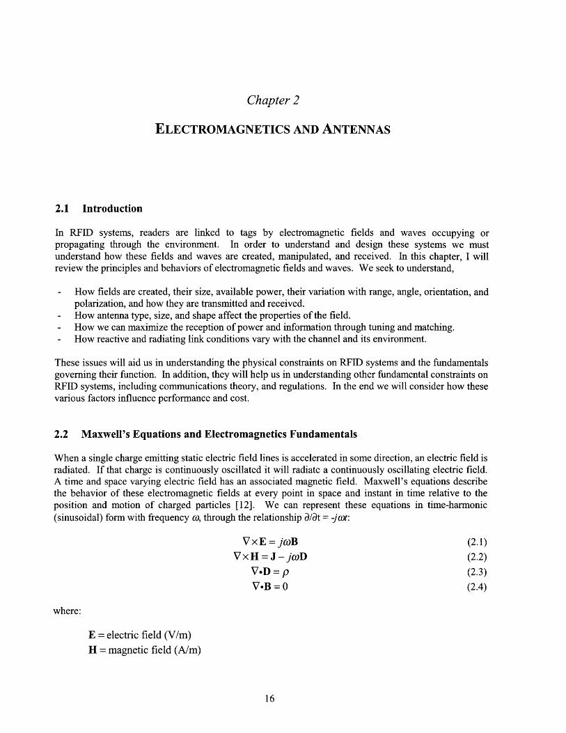
I will consider only the components of the system that interact directly with the function of the tags,namely the tag interface portion of the reader, the tags themselves, and the communications channel. Thefunctions performed by these components along with the specifications and constraints that govern theirdesign, are shown in Figure 1.2.
II
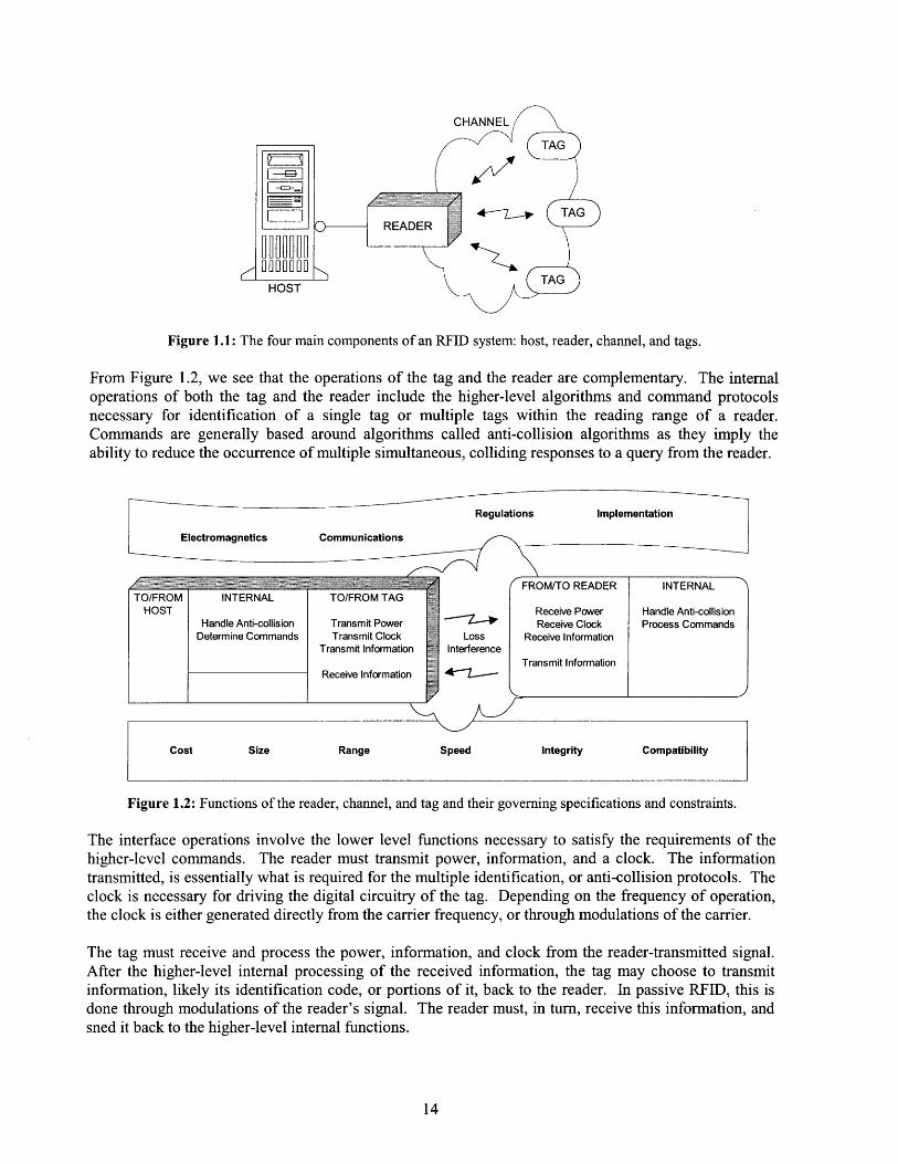
Figure 1.1: The four main components of an RFID system: host, reader, channel, and tags.
From Figure 1.2, we see that the operations of the tag and the reader are complementary. The internaloperations of both the tag and the reader include the higher-level algorithms and command protocolsnecessary for identification of a single tag or multiple tags within the reading range of a reader.Commands are generally based around algorithms called anti-collision algorithms as they imply theability to reduce the occurrence of multiple simultaneous, colliding responses to a query from the reader.
Figure 1.2: Functions of the reader, channel, and tag and their governing specifications and constraints.
The interface operations involve the lower level functions necessary to satisfy the requirements of thehigher-level commands. The reader must transmit power, information, and a clock. The informationtransmitted, is essentially what is required for the multiple identification, or anti-collision protocols. Theclock is necessary for driving the digital circuitry of the tag. Depending on the frequency of operation,the clock is either generated directly from the carrier frequency, or through modulations of the carrier.
The tag must receive and process the power, information, and clock from the reader-transmitted signal.After the higher-level internal processing of the received information, the tag may choose to transmitinformation, likely its identification code, or portions of it, back to the reader. In passive RFID, this isdone through modulations of the reader's signal. The reader must, in turn, receive this information, andsned it back to the higher-level internal functions.

1.6.2 Constraints and Organization
The design and implementation of these various functions is determined by both the specifications andfundamental constraints. These constraints include the electromagnetics and communications, whichdefine the methods by which the tag and reader can communicate, and the regulations and hardwareconstraints, which impose limits on these methods.
In Chapter 2, I will discuss the electromagnetic fields and waves that link the reader to the tag. I willdescribe how they are created by antennas and how their characteristics and behavior vary with operatingfrequency and distance from the antenna. I will describe how RFID systems exploit these characteristicsto achieve power and communications coupling. Finally, I will cover the various environmentalinfluences on the behavior of fields and waves, and the coupling between reader and tag.
In Chapter 3, I will discuss the communications between the reader and tag and the theory that describesit. I will discuss and analyze the characteristics of the various coding and modulation schemes commonlyused in RFID. I will consider detection methods and concerns related to the integrity of communicationsand error detection.
In Chapter 4, I will consider the regulations that govern both the electromagnetics and communications. Iwill consider regulations imposed by bodies in three different regions of the world, Europe, the UnitedStates, and Japan. I will discuss their various methods of specifying regulations and the implications thishas for RFID systems.
In Chapter 5, I will discuss constraints related to physical implementation of the hardware. I will discussthose properties of antennas that affect performance, cost, and size. I will also consider the integratedcircuit and how its design and implementation affects performance and cost.
In Chapter 6, I will discuss and analyze anti-collision methods and the command protocols necessary todrive the identification of multiple tags within the range of a reader.
In Chapter 7, I will relate the fundamental constraints to the important performance specifications, anddiscuss their interactions.
Finally, in Chapter 8, I will conclude and present directions for future work.
Chapter 2
ELECTROMAGNETICS AND ANTENNAS
2.1 Introduction
In RFID systems, readers are linked to tags by electromagnetic fields and waves occupying orpropagating through the environment. In order to understand and design these systems we mustunderstand how these fields and waves are created, manipulated, and received. In this chapter, I willreview the principles and behaviors of electromagnetic fields and waves. We seek to understand,
- How fields are created, their size, available power, their variation with range, angle, orientation, andpolarization, and how they are transmitted and received.
- How antenna type, size, and shape affect the properties of the field.- How we can maximize the reception of power and information through tuning and matching.- How reactive and radiating link conditions vary with the channel and its environment.
These issues will aid us in understanding the physical constraints on RFID systems and the fundamentalsgoverning their function. In addition, they will help us in understanding other fundamental constraints onRFID systems, including communications theory, and regulations. In the end we will consider how thesevarious factors influence performance and cost.
2.2 Maxwell's Equations and Electromagnetics Fundamentals
When a single charge emitting static electric field lines is accelerated in some direction, an electric field isradiated. If that charge is continuously oscillated it will radiate a continuously oscillating electric field.A time and space varying electric field has an associated magnetic field. Maxwell's equations describethe behavior of these electromagnetic fields at every point in space and instant in time relative to theposition and motion of charged particles [12]. We can represent these equations in time-harmonic(sinusoidal) form with frequency co, through the relationship a/lt = -jot:
VxE = jeoB (2.1)
Vx H = J - jcoD (2.2)V-D = p (2.3)
VB = 0 (2.4)
where:
E = electric field (V/m)
H = magnetic field (A/m)
B = magnetic flux density (T)
D = electric displacement (C/m 2 )
J = electric current density (A/m 2)
p = electric charge density (C/m 3)
The continuity equation for the conservation of charge and current is given as
jcwp + V -J = 0 (2.5)
Together with Maxwell's equations, they form the fundamental equations of electromagnetics.
The time averaged power per unit area delivered through a surface by electric and magnetic fields is givenby Poynting's vector:
S= Re{ExH*} (2.6)
where H* is the complex conjugate of H, and S is a power density having units of W/m 2.
In a region with no charge or current densities, an electric field, coupled with and orthogonal inpolarization to a magnetic field, will propagate through a given medium in a direction perpendicular toboth fields. This is an electromagnetic wave. An antenna is designed to radiate electromagnetic fieldsand waves.
In further discussion we will use several parameters to describe fields and waves. These parameters canbe given in general form for describing interactions with any material. We will focus on those for loss-less media and free-space. The free-space wavenumber is given by
ko oeo = _ 0 2= = = f= (2.7)
where:
c = speed of light 3 3x10⁸(m/s)
Eo = free space permittivity = 8.8542x 10⁻¹² (F / m)
Y0 = free space permeability = 4r x 10- 7 (H / m)
The permittivity relates the electric field E to the electric displacement D through D = EoE. Thepermeability relates the magnetic field H to the magnetic flux B through B = /oH.
Another useful parameter is the free-space impedance
770 =- r (2.8)0 E
Through the fundamental equations of electromagnetics and these various parameters, we can understandhow field and waves are created.
2.3 Antennas and Their Surrounding Regions
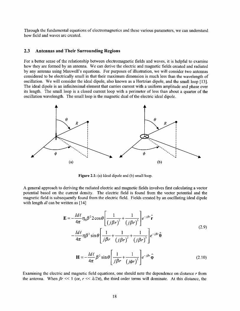
For a better sense of the relationship between electromagnetic fields and waves, it is helpful to examinehow they are formed by an antenna. We can derive the electric and magnetic fields created and radiatedby any antenna using Maxwell's equations. For purposes of illustration, we will consider two antennasconsidered to be electrically small in that their maximum dimension is much less than the wavelength ofoscillation. We will consider the ideal dipole, also known as a Hertzian dipole, and the small loop [13].The ideal dipole is an infinitesimal element that carries current with a uniform amplitude and phase overits length. The small loop is a closed current loop with a perimeter of less than about a quarter of theoscillation wavelength. The small loop is the magnetic dual of the electric ideal dipole.
(a) (b)
Figure 2.1: (a) Ideal dipole and (b) small loop.
A general approach to deriving the radiated electric and magnetic fields involves first calculating a vectorpotential based on the current density. The electric field is found from the vector potential and themagnetic field is subsequently found from the electric field. Fields created by an oscillating ideal dipolewith length dl can be written as [14]
Id o12 2c [ 1 1 -j- r4r 22cos6 I + eIp r e4r (j/3r)2 (j3r)3 e
F (2.9)
di 2 L 1 1 (10H Id sinO 1 1 e-H= - j spr r (2.10)4•r j/3r (jpr)
Examining the electric and magnetic field equations, one should note the dependence on distance r fromthe antenna. When fir << 1 (or, r << A/2n), the third order terms will dominate. At this distance, the
electric field strength decays as 1/r3, and the magnetic field strength decays as 1/r2. We will refer to thisregion as the near-field.
When the distance r is much greater than 2/2ir, the first order terms dominate, and both the electric fieldand magnetic field strengths decay as 1/r. We will refer to this region as the far-field.
Examining these equations further, we notice that in the near-field where fir << 1, not only does the thirdorder term dominate, but e-•pr also approaches 1. The electric and magnetic fields reduce to
E" = j 4 3 0 (2cos6r +sin ) (2.11)
Id .H"' = s2 ine8 (2.12)
Beyond the dissimilar relationship with distance r indicating dissimilar decay, we note that the electricfield is imaginary, indicating it is 2/4 (90 degrees) out of phase with the magnetic field. This is anindication of a reactive field - energy is essentially stored and released between the two fields.Evaluating the Poynting vector for this case further reveals that there is no real power flow. Theelectromagnetic fields in the near-field are essentially decoupled from each other and quasi-static.Further simplification will reveal that the small dipole is essentially behaving as a static electric dipole.
In considering the far-field where fir >> 1, the first order terms dominate and the field equations reduce to
Idf -j inrE = j - 0ioPe' sin 0 (2.13)
41r
H" = j Pejpr sinO9 (2.14)41 r
We immediately see that the electric and magnetic fields are in phase, orthogonal in polarization, andrelated in magnitude by E/HO-=77o, the intrinsic impedance of free space. Both fields decay as 1/r.Evaluation of the Poynting vector reveals a real power density, indicating propagation through a surface.The electromagnetic fields in the far-field constitute an electromagnetic wave.
We can also consider the fields for a small loop antenna,
Icd £1 1 _ _
E= 0 2 jr (2.15)E 4•r sin0 jPr + ejr)
S 4 I 1 1 +
Id 2 sinO + j+ r -j r4 jp' r (jr) . 3
The near-field components are
Id?E"a = 2 0 sin 0 (2.17)
HId= (2cosOr+sinO ) (2.18)
and the far-field components are
H 1 j pejr sin0O (2.19)
Id £Ef = -j ro0Pe-j' sin p (2.20)
4w r
Noting the similarities between the ideal dipole and the small loop field equations, we see that the smallloop is the dual of the ideal dipole.
There is yet another region is of concern, often called the Rayleigh region. In this region, it becomesreasonable to approximate a spherical electromagnetic wave as a uniform plane wave. Plane waves arethose with an electric field with the same direction, magnitude, and phase in infinite planes, perpendicularto the direction of propagation. They do not exist in practice, as they would require infinitely sizedsources. However, at a distance far enough from the source, this approximation becomes reasonable. Thisregion is given by
2D 2r > (2.21)
where r is the distance from the antenna, and D is the length of a radiating line source. When we discusselectromagnetic waves, we will not only assume we are in the far-field, but also in the Rayleigh region.
In addition to understanding the relationship between electromagnetic fields and waves, we also see thatelectromagnetic fields exhibit radically different behavior in the near-field zone as compared with the far-field zone. In the near-field, fields are reactive and quasi-static, while in the far-field they constituteradiated waves. This result is particularly important to RFID systems. Those systems operating at lowerfrequencies where the near-field encompasses the operating range, must achieve coupling through thequasi-static fields. RFID systems operating at higher frequencies typically operate in the far field andachieve coupling through electromagnetic waves.
We should note that the transition point between near-field and far-field is actually dependent on theantenna geometry. However, we will use the transition point of 2/27 as the standard definition.
2.4 Impedance of Space, Antennas, and Circuits
Before further analyzing the behavior of RFID systems operating in the near-field and far-field, it will behelpful to discuss the concept of impedance as it relates to free-space, antennas, and circuits. In general,impedance describes the relationship between an effort and a flow. In electromagnetic field and wavetheory, impedance is the relationship between the electric field and the magnetic field.
EZ = (2.22)
H
In an antenna or electrical circuit, it is the relationship between the voltage and the current.
VZ = -(2.23)
I
Regardless of domain, it is an extremely useful parameter capable of characterizing the behavior of fieldsand waves, radiation and reaction of an antenna, and power transfer between an antenna, transmissionline, and load.
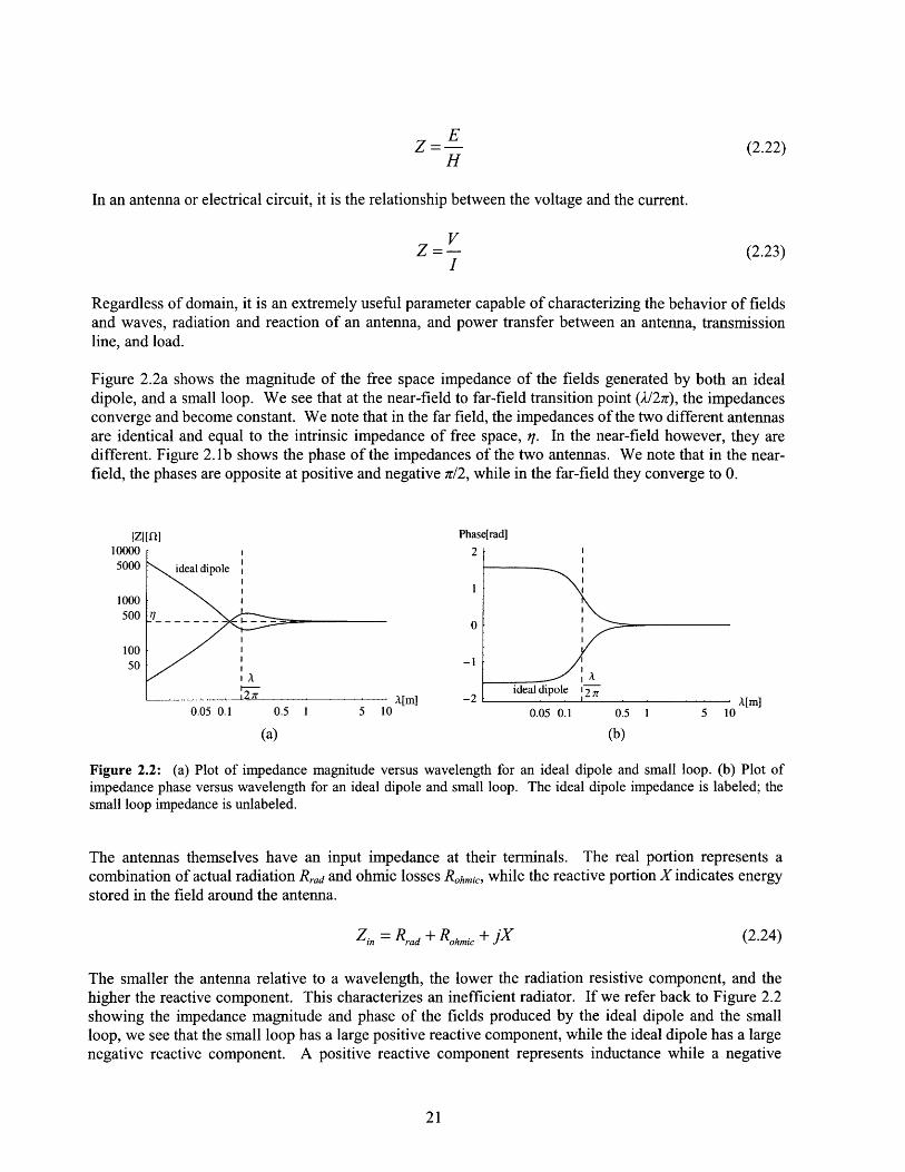
Figure 2.2a shows the magnitude of the free space impedance of the fields generated by both an idealdipole, and a small loop. We see that at the near-field to far-field transition point (2/2r), the impedancesconverge and become constant. We note that in the far field, the impedances of the two different antennasare identical and equal to the intrinsic impedance of free space, q. In the near-field however, they aredifferent. Figure 2. lb shows the phase of the impedances of the two antennas. We note that in the near-field, the phases are opposite at positive and negative r/2, while in the far-field they converge to 0.
IZI M[] Phase[rad]I 100U0
5000
1000500
10050
1
0
-1
•rml --?
S lideal dipole 12 ir.... r
0.05 0.1 0.5 1 5 10 0.05 0.1 0.5 1 5 10
(a) (b)
Figure 2.2: (a) Plot of impedance magnitude versus wavelength for an ideal dipole and small loop. (b) Plot ofimpedance phase versus wavelength for an ideal dipole and small loop. The ideal dipole impedance is labeled; thesmall loop impedance is unlabeled.
The antennas themselves have an input impedance at their terminals. The real portion represents acombination of actual radiation Rrad and ohmic losses Rohmic, while the reactive portion X indicates energystored in the field around the antenna.
Zin = Rrad + Rohmic + jX (2.24)
The smaller the antenna relative to a wavelength, the lower the radiation resistive component, and thehigher the reactive component. This characterizes an inefficient radiator. If we refer back to Figure 2.2showing the impedance magnitude and phase of the fields produced by the ideal dipole and the smallloop, we see that the small loop has a large positive reactive component, while the ideal dipole has a largenegative reactive component. A positive reactive component represents inductance while a negative
reactive component represents capacitance. This is particularly important to RFID systems that operate inthe near-field.
As the antenna size increases relative to the wavelength, the radiation resistance component increases,while the reactive component decreases. At a length or perimeter of a half-wavelength the reactivecomponent approaches zero while the resistive component reaches its maximum. At this dimension, theantenna is resonant and radiates efficiently. Far-field systems typically use resonant antennas. Increasingthe size further, however, results in an increase in the reactive component and a decrease in the resistivecomponent, until at a dimension of a wavelength, the impedance is similar to what it was at aninfinitesimal dimension. This cycle repeats for every multiple of a wavelength.
Transmission lines and electric circuits, too, have an impedance. As described by transmission linetheory, for maximum power transfer, impedances must be conjugate matches. Real components shouldbe equal, while reactive components should be equal and opposite. We will see in the following sectionshow this affects the operation of RFID systems.
2.5 Coupling in the Near Field and Far Field
We will now consider the antennas and fundamental principles necessary for communications and energycoupling for operation in either the near-field or the far-field. Due to the difference in electromagneticfield behavior in each region, methods are significantly different and I will treat them separately. In thenear-field, coupling is between a source and a sink as opposed to the far-field, where it is between atransmitter and receiver.
2.5.1 Near-field Coupling
As I have previously shown, electromagnetic fields in the near-field are reactive and quasi-static innature. The electric fields are decoupled from the magnetic fields, and depending on the type of antennaemployed, one will dominate the other. In the case of the ideal dipole, the electric field dominates, whilein the case of the small loop, the magnetic field dominates. Coupling may be achieved capacitivelythrough interaction with the electric field, or inductively through interaction with the magnetic field.Among near-field RFID systems, inductively coupled systems are more widely available thancapacitively coupled systems. Thus I will emphasize inductively coupled systems.
In this section, I will describe the principles of and present relations governing both inductive andcapacitive coupling. I will describe how energy is coupled, and how communications can be attained.
2.5.1.1 Inductive Coupling
Antennas for systems employing inductive coupling rely on interaction with the quasi-static magneticfield. Essentially these systems are transformers where current running through a primary coil induces amagnetic field, which then induces a current and voltage in a secondary coil. In the case of RFID, theprimary coil is attached to the reader while the secondary coil is attached to the tag. A small loop antennais preferred to a dipole antenna because the near-field magnetic field created by the small loop dominatesthat created by the dipole.
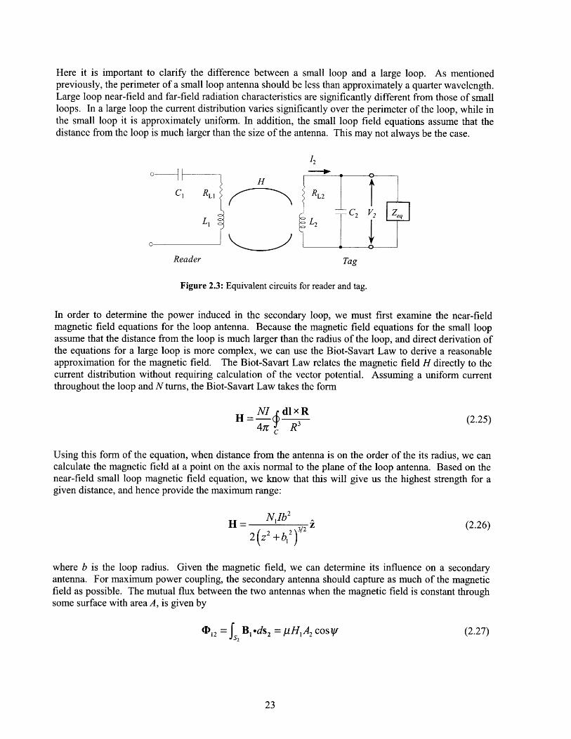
Here it is important to clarify the difference between a small loop and a large loop. As mentionedpreviously, the perimeter of a small loop antenna should be less than approximately a quarter wavelength.Large loop near-field and far-field radiation characteristics are significantly different from those of smallloops. In a large loop the current distribution varies significantly over the perimeter of the loop, while inthe small loop it is approximately uniform. In addition, the small loop field equations assume that thedistance from the loop is much larger than the size of the antenna. This may not always be the case.
12
H
K 2Reader Tag
Figure 2.3: Equivalent circuits for reader and tag.
In order to determine the power induced in the secondary loop, we must first examine the near-fieldmagnetic field equations for the loop antenna. Because the magnetic field equations for the small loopassume that the distance from the loop is much larger than the radius of the loop, and direct derivation ofthe equations for a large loop is more complex, we can use the Biot-Savart Law to derive a reasonableapproximation for the magnetic field. The Biot-Savart Law relates the magnetic field H directly to thecurrent distribution without requiring calculation of the vector potential. Assuming a uniform currentthroughout the loop and N turns, the Biot-Savart Law takes the form
NI ~dlxRH = N7 d(2.25)
Using this form of the equation, when distance from the antenna is on the order of the its radius, we cancalculate the magnetic field at a point on the axis normal to the plane of the loop antenna. Based on thenear-field small loop magnetic field equation, we know that this will give us the highest strength for agiven distance, and hence provide the maximum range:
NIb2H = NIb2 (2.26)
2 ( z2+b 2)
where b is the loop radius. Given the magnetic field, we can determine its influence on a secondaryantenna. For maximum power coupling, the secondary antenna should capture as much of the magneticfield as possible. The mutual flux between the two antennas when the magnetic field is constant throughsome surface with area A, is given by
(DI2 B1°ds2 = IHA 2 cosY/ (2.27)1 2s
where ~y is the angle between the field lines at the surface normal. A mutual inductance L12 can beexpressed in terms of the mutual flux:
L12 N2 12 (2.28)I1
As given by Lenz's Law, the negative time rate of change of this mutual flux induces a voltage in thesecondary loop:
2 -N2 =jN 2 , 12 (2.29)dt
Because the secondary loop and the attached circuit has some equivalent impedance, the voltage Vl, 2generates a finite current 12. This current produces an additional magnetic flux which opposes the initialflux due to the secondary loop's self inductance L2. This flux causes a voltage drop V2- 2 , where
dl
V2-2 = -L 2 = jL2 2 (2.30)
The self inductance of a small circular loop is given by [13]
L2 = bN2[In (j-j1.75 (2.31)
where b is the loop radius, a is the wire radius, and a << b.
The secondary loop also has an associated resistance that produces an additional voltage drop.
VRL 2 = I2 RL2 (2.32)
where ohmic resistance for a small circular loop antenna is given by [13]
R! = N 2 -b (2.33)a F20
Combining the mutually induced voltage, the self induced voltage, and the resistive component of thevoltage gives the total voltage across the secondary loop V2.
V2 -= Vl2 - V2-2 - VR (2.34)
Substituting (2.27), (2.29), (2.30), and (2.32) into (2.34), we find
V2 = jOwN 2 oH1A2 cosy/ -12 (jwL 2 +R, ) (2.35)
The same relations hold for induction from the secondary to the primary, in RFID, the tag to the reader.
S= jcwN1 0oHA , cosvr-I, (jcL, + R ) (2.36)
2.5.1.1.1 Resonance and Q
To maximize the power available to the secondary circuit at a given frequency, it is necessary to createLC resonant circuits in both the tag and the reader. The resonant frequency of an LC circuit is given by
1C)LC =- (2.37)
In the case of the reader we wish to maximize the output current for maximum field strength, so we add acapacitance in series with a loop to create an impedance that approaches zero at the resonant frequency.In the case of the tag, we wish to maximize voltage to drive the tag circuitry, so we add a capacitance inparallel with the loop to create an impedance that approaches infinity at the resonant frequency. Becausethere is resistance inherent in the loops, connections, and other components, there is some quality factor Qassociated with both the tag and the reader. Q is defined as the ratio of energy stored to energy dissipatedor as the ratio of the center frequency of operation to the 3dB bandwidth. It can be expressed as:
oL foQ = or Q = (2.38)
R Af3dB
To maximize Q, we may either reduce the resistance, increase the reactance associated with the loops, orboth. For a single frequency, maximum Q is desirable for maximum power coupling. But, because ahigh Q implies a narrow bandwidth, it must be low enough to allow for sufficient communications.Bandwidth as related to communications will be discussed in Chapter 3. This tradeoff will be revisited inChapter 5.
2.5.1.1.2 Load Modulation
These relations between magnetic field strength and voltage induction, apply to both reader to tag powertransfer and communications, and tag to reader communications. Tag to reader communications isachieved through variation of the tag's impedance. By varying its impedance, the tag varies the currentthrough its loop, which alters the magnetic field. This change is subsequently detected by the reader.
The tag varies its impedance by either switching resistances or capacitances; hence there is both ohmicload modulation and capacitive load modulation [6]. In ohmic modulation, a resistance in parallel withthe load is switched on or off, either in time with the data stream, or at some higher frequency(subcarrier). The parallel resistance reduces the effective resistance, which causes a higher current in thetag. This results in a voltage drop at the reader. The signal is essentially amplitude modulated.
In capacitive load modulation, a capacitance in parallel with the load is switched on or off just as with theresistor in ohmic modulation. These changes are detected by the reader as a combination of amplitudeand phase modulation.
2.5.1.1.3 Voltage Available to Load
With the resonance capacitor in parallel with the equivalent impedance of the attached circuitry, we cansimplify the expression for voltage in the tag. Referring to Figure 2.3, first we find the current I2 throughthe tags loop as a function of the parallel equivalent impedance of the resonance capacitor and theadditional circuitry equivalent impedance.
2= 2/ = V2 + joC2 (2.39)
Substituting this into Eq. (2.35) we find
j oN 2 0oH,A2 cos(fV2 = (2.40)
V 1+ (jL 2 ±+ R) + jwC2eq
This is the voltage available to a load in parallel with the loop antenna. Current through the load issimply found by Ohm's Law based on the impedance of the load. Power consumed by the load can thenbe determined. It is clear from Eq. (2.40) that the voltage increases with number of turns, the magneticfield strength, loop area, and orientation. The effect of the circuit parameters is not as clear. Togetherthey define the resonant frequency and bandwidth. It should be apparent that the equivalent loadimpedance also influences the resonance.
2.5.1.2 Capacitive Coupling
In capacitively coupled systems, antennas create and interact with quasi-static electric fields. In thesesystems it is the distribution of charges rather than currents that determines the field strength and henceinfluences the coupling strength. Because coupling strength is dependent on amount of collected charge,rather than current, conductivity can be less important than in inductive systems [15]. However,capacitively coupled systems can suffer due to environmental affects, as I will discuss later in the chapter.
A wire or a plate dipole is a suitable antenna for capacitively coupled systems since the electric fielddominates the magnetic field. If considering a dipole antenna for both primary and secondary antennas, arough approximation for the electric field can be made by using that of the ideal dipole. However, thiswould assume that the distance between the primary and secondary antennas would be much greater thanthe length of the antenna. This may not be the case. Thus, we can derive the electric field for a wiredipole antenna of length L, with uniform charge distribution p, from the following equation:
E = -•dL (2.41)47cE R 3
The charge collected on a surface S can be found from a derivation of Ampere's Circuital Law:
Q = EfsE.dS (2.42)
A time varying electric field will induce a current through the secondary antenna. The secondary antennahas its own impedance consisting of capacitance across its electrodes, and resistance associated with theantenna and other materials. Given some equivalent impedance within the antenna and the attachedcircuit, the induced current will generate a voltage potential across each element.
2.5.1.2.1 Resonance and Load Modulation
Just as inductively coupled systems require resonant circuits for maximum coupling, so do capacitivelycoupled systems. Since the antenna has its own capacitance, inductance is added in parallel on the tagand in series in the reader. In addition, like in the inductively coupled systems, the tag can communicatewith the reader through varying its impedance.
Whether a system is inductively coupled or capacitively coupled, we wish to maximize coupling forpurposes of power transfer and communication. In the case of coupling through transmission andreception of electromagnetic waves, the goals are the same, though the mechanisms are quite different. Iwill discuss these mechanisms in the next section.
2.5.2 Far-field Coupling
As is common in most wireless communications systems, coupling in systems operating in the far-field isachieved through transmission, propagation, and reception of electromagnetic waves. After presentingsome useful relations for electromagnetic fields, I will discuss the performance parameters necessary fordescribing the radiating properties of an antenna. I will next discuss the transmission and reception ofelectromagnetic waves, focusing on the power available to a receiving antenna and its attached load.
2.5.2.1 Antenna Parameters
We have already considered electrically small dipole and loop antennas. These antennas are noted fortheir high reactance (whether it be capacitive or inductive), inefficient radiation characteristics, anddifficulty in matching. While suitable for operation in the near-field, they are generally not suitable forfar-field operation where transmission and, particularly, reception should be efficient. For this reason,resonant antennas characterized by a dimension on the order of one half the wavelength of transmittedfrequency, are commonly used. Resonant antennas offer more efficient radiation and reduced reactivity.Bandwidth, however, can be narrow. Types commonly used in RFID systems include half-wave dipoleand microstrip patch antennas. Certain physical characteristics of these antennas will be discussed inChapter 5.
The waves radiated by all antennas consist of electric and magnetic fields related by the free-spaceimpedance. The field magnitudes vary with antenna type and output power, but both decay with theinverse of distance from the source. The angular distribution of radiation, however, varies with the typeof antenna.
We use the radiation pattern to describe the angular distribution of an antenna's radiation. An antennaradiation pattern is given in terms of the normalized electric field distribution over a constant distance r.In the case where a z-directed source has an electric field with only a theta component, the radiationpattern can be given as,
F(0,0)= o (2.43)E, (max)
In the case where there is phase variation, the phase is generally set to 0 at the point where the electricfield is at its maximum. In this way relative phase can be described.
Certain antennas may be able to concentrate their fields into a narrower beam of radiation. In doing sothe power density will increase relative to distance, allowing transmission at longer ranges. The termdirectivity is used to describe how an antenna concentrates its energy in one direction as compared toevery other direction. It is defined as the ratio of radiation intensity in a certain direction to the averageradiation intensity.
Directivity is solely based on an antenna's radiation pattern. It is often useful, however, to describe notonly the directive properties of an antenna but its efficiency in transforming some input power to radiatedoutput power. The term gain quantifies this. Typically it is defined as 4n times the ratio of radiationintensity in a given direction to the net power input of the antenna.
G(, ) = ,) (2.44)
When referring to gain simply as G, we will be referring to maximum gain.
Gain is often described by comparing the maximum radiation intensity of one antenna to the maximumradiation intensity of some standard reference antenna. Typically we will describe an antenna's gainrelative to an isotropic radiator that radiates energy in all directions uniformly. Also, in certain instancesgain will be described relative to a half-wave dipole. Gain is typically given in units of decibels (dB). Anisotropic radiator has a gain of 0 dB, while a half-wave dipole antenna has a gain of 2.15 dB. Whendescribing the gain relative to an isotropic radiator we describe this by units of dBi. When describinggain relative to a half-wave dipole antenna, we use units of dBd. If we consider an antenna with a gain of6 dB, it can be described by a gain of 6 dBi, or 3.85 dBd [13].
G [dB]= G [dBi]= Gd [dBd]+ 2.15 dB (2.45)
Unless otherwise specified, when referring to gain, we will be referring to gain relative to an isotropicradiator.
Just as gain can be described relative to some standard reference antenna, so to can be the radiated power.We often use effective (or equivalent) isotropically radiated power, EIRP, defined as the net input powerto an antenna multiplied by its gain relative to an isotropic antenna.
EIRP = GtP (2.46)
We may also use effective radiated power, ERP, which is simply the net input power to an antennamultipled by its gain relative to a half-wave dipole antenna:
ERP = PGtd (2.47)
EIRP is related to ERP by
EIRP = ERP x 1.64
With these parameters we can now consider the transmission and reception of waves.
2.5.2.2 Transmission and Reception
In considering the operation of RFID tags, we must determine the power available at the tag antenna. Thetag will absorb some of this power for powering itself and detecting information. It will also scatter someof this power for transmitting information back to the reader. To understand this process we will firstdetermine the power available to the tag given the transmitted power and gain at the reader. We will thendetermine the power delivered to the tag's load. Finally, we will consider the scattering of power back tothe reader for communications.
2.5.2.3 Reader to Tag Transmission
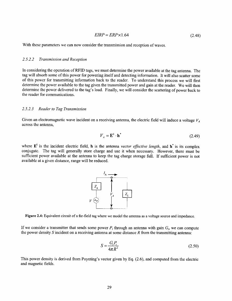
Given an electromagnetic wave incident on a receiving antenna, the electric field will induce a voltage VAacross the antenna,
V =-- l'.h* (2.49)
where E' is the incident electric field, h is the antenna vector effective length, and h* is its complexconjugate. The tag will generally store charge and use it when necessary. However, there must besufficient power available at the antenna to keep the tag charge storage full. If sufficient power is notavailable at a given distance, range will be reduced.
Figure 2.4: Equivalent circuit of a far-field tag where we model the antenna as a voltage source and impedance.
If we consider a transmitter that sends some power Pt through an antenna with gain G,, we can computethe power density S incident on a receiving antenna at some distance R from the transmitting antenna:
G4PR2
4rcR 2 (2.50)
This power density is derived from Poynting's vector given by Eq. (2.6), and computed from the electricand magnetic fields.
(2.48)
u Ir
Ati " ,
From this power density, it is useful to define an effective aperture Ae, which is based on the antenna'sown gain. It essentially can be thought of as a power capture area:
A, (, 0)= • G(O, ) (2.51)41r
When simply denoted as Ae without the dependence on angle, it represents the maximum effective area.
Simply multiplying the effective aperture by the power density should give the power received by thereceiving antenna. However, we must also consider potential polarization mismatch issues. If theantenna has some polarization that is different from that of the incoming wave, only a fraction of thepower will be received. For this reason, we define a polarization mismatch factor, p, to account for thepotential polarization mismatch [13]. It is given as,
P I h* 2 (2.52)IE' 2 Ihl2
where E' and h are defined as in (2.49). When there is no polarization mismatch, p is 1.
We can now compute the power received by the receiving antenna:
GPtAer, (0) (2.53)P, = pSAe, (0, ) = p 4R 2 (2.53)
Substituting for Aer, in terms of G, using Eq. (2.51) and Eq. (2.53) becomes:
S(4rR)2 (2.54)(41R)2
This gives the power received by the antenna, yet as there is some load in the attached circuitry, we mustconsider the power available to the load. For maximum power transfer from the antenna to the load, wemust match the impedance of the antenna with the load equivalent impedance. In cases where a conjugatematch between the load and antenna impedances is achieved, the power available to the load is thatreceived by the antenna. In other circumstances we include an impedance mismatch factor q [13]:
PD 4RARLq - - 24 R (2.55)PDm.x (RA +RL) 2 +(XA +XL
When a conjugate match is achieved between the antenna impedance ZA and the load impedance ZL, q is1. With q we can find the power delivered to the load resistance RL:
Gt GGA2PD = qP = qpPt (2.56)
(41rR)2
The fraction of Pt not delivered to the load (1-q) is scattered. In the following section, I will discussscattering.
2.5.2.4 Backscatter Modulation
Much as near-field RFID tags achieve communications with a reader by varying their load impedance, sodo far-field tags. In the far-field, however, variation of the tag's load impedance causes an intendedmismatch in impedance between the tag's antenna and load. This causes some power to be reflected backthrough the antenna and scattered, much like the antenna is radiating its own signal. The return scatteredsignal is detected and decoded by the reader. This form of communication is called backscattermodulation. After briefly reviewing the general concept of scattering, I will focus on scattering byantennas. I will then relate the power available at the antenna and delivered to a load to that scatteredback to the source.
2.5.2.4.1 Scattering
When an electromagnetic wave impinges on irregularities in a medium, the wave may be randomlydispersed. This phenomenon is called scattering. In sensor systems such as radar and RFID, a transmitterwill transmit a radio-frequency electromagnetic wave and a receiver will detect an object's scatteredresponse. When the receiver is collocated with the transmitter, scattering is referred to as monostatic, orbackscatter. Modulated backscatter RFID systems achieve communications through controlled changesof a tag's backscatter response
A useful representation of an object's monostatic scattering characteristics is its backscattering crosssection or radar cross section (RCS). After briefly reviewing the definition of scattering and radar cross-section, I will describe the basic principles of modulated backscatter in the context of RFID systems. Iwill then discuss, in more detail, the factors influencing RFID tag and reader design.
2.5.2.4.2 Scattering and Radar Cross Section
The IEEE defines scattering in radio wave propagation as "a process in which the energy of a travelingwave is dispersed in direction due to interaction with inhomogeneities of the medium" [16]. It resultswhen electromagnetic waves impinge upon an object and induce oscillating charges and currents withinthe object and on its surface and hence an electromagnetic field. We can determine these scattered fieldsthrough numerical or analytical evaluation of the induced surface charges and currents, or through the useof the tangential field approximation as used in physical optics [17]. In general, the spatial distribution ofthe scattered energy depends on size, shape, and composition of the object, and the waveform, anddirection of its arrival.
Radar cross section (RCS), has been defined as a measure of power scattered in a given direction. It isexpressed as an area much like an antenna's effective aperture. The IEEE defines it as,
... 4x times ratio of the power per unit solid angle scattered in a specified direction to the powerper unit area in a plane wave incident on the scatterer from a specified direction. More precisely,it is the limit of that ratio as the distance from the scatterer to the point where the scattered poweris measured approaches infinity... [16]
Three cases are given: monostatic or backscattering RCS, where incident and pertinent scatteringdirections are coincident but opposite in sense, forward scattering RCS where the two directions andsenses are the same, and bistatic RCS where the two directions are different. If not specified, RCS isassumed to be monostatic. It is further mentioned that RCS is a function of frequency, transmitting andreceiving polarizations, and target aspect angle. It can be represented symbolically as,
o = lim 41rR 2 Escat (2.57)R• " Einc 2
where Escat is the scattered electric field, E'"i is the incident electric field, and R is the distance from thetarget. In another form, RCS is given as
a = 4rR2 s (2.58)
where P, is the power scattered and Pi is the incident power.
Scattering can be characterized by three regimes based on the ratio of the wavelength 2 to body size L.These regimes are the Rayleigh region (not to be confused with the far-field plane wave region given byEq. (2.21)), the resonant region, and the optics region. In the Rayleigh region, the wavelength is muchgreater than the body size so there is little variation in phase over the length of the body. As the bodyessentially sees a quasistatic field, a dipole moment is induced resulting in a scattered field. In theresonant region, the wavelength is on the order of the body size - typically the body size is taken to bebetween 1 and 10 wavelengths. In this region, the electromagnetic energy shows a tendency to stayattached to the body's surface creating surface waves including traveling waves, creeping waves, andedge traveling waves. In the optics region, the wavelength is much less than the body size. Here thedominating scattering mechanisms are specular scattering, end-region scattering, diffraction, and multiplereflections [17].
As we are concerned with backscatter from antennas with size on the order of a wavelength, we areprincipally concerned with scattering in the resonant region where surface wave scattering dominates.We are unable to use the tangential plane approximation, as it is essentially only useful for evaluation ofspecular scattering. Instead we must solve for the scattered field based on the induced surface currentsand charges. As an analytical solution can be difficult, the various methods, including the method ofmoments can provide a numerical solution [17].
2.5.2.4.3 Antenna Scattering
In analyzing modulated backscatter tags, we are most concerned with the scattering characteristics of thetag's antenna. Because antennas are designed to transmit and receive radiation, they are generallyregarded as having two modes of scattering. One, the structural mode, is the scattering that occursbecause a given antenna is a certain shape, size, and material. The other, the antenna mode, is thescattering that occurs because the antenna was designed to transmit RF energy and has a specific radiationpattern. It should be noted that there are no formal definitions of these modes, and variations exist[17][13].
There have been several models given for the field scattered from an antenna [18][19]. I will use the onepresented by Green [19]. Referring to Figure 2.4, the scattered field as a function of load impedance ZL isgiven by
E(ZL) = E(Z )+ FI(Z,)Er (2.59)
where the modified reflection coefficient gamma is given by
z -zF = A L (2.60)
ZA +ZL
and Er is the far-field electric field when the antenna is excited by a unit current source, given by
Er = - j e r'h (2.61)41rr
Comparing this equation to the far-field electric field for an ideal dipole Eq. (2.13), we see that h =dlsinO0 in the case of an ideal dipole. This will be different for practical antennas. The negative signrepresents the reflection. E(ZA*) and I(ZA*) in Eq. (2.59) represent the scattered field and antenna currentwhen the load impedance is a conjugate match of the antenna impedance, respectively. The second termin Eq. (2.59) is the antenna mode scattering. It is related directly to the load impedance connected to theantenna. When the load impedance is matched with the antenna impedance, this term goes to zero,leaving the first term called the structural mode scattering.
Analytical derivation of the structural mode scattering can be difficult and will typically require methodssuch as the method of moments. If we choose to neglect it, the RCS of the antenna mode scattering canbe given in terms of the familiar antenna parameters,
A2
Uant = pF 2 G2 (6,0) (2.62)41r
where p is the polarization factor from Eq. (2.52) accounting for a mismatch in polarization between theincident field and the scattering antenna. Additionally, Green considers the case where the load isswitched between two different loads with modified reflection coefficients F, and F2. In effect, thiscancels the static structural mode. The modulation of the scattered field becomes
4ARA r
The associated radar cross section becomes
A2
UA = p2 1 2 2 G2 (6,4) (2.64)41r
These equations show the basis of backscatter modulation. By varying the load impedance, tags are ableto modulate the amplitude and phase of the backscattered field.
2.5.2.4.4 Power Scattered and Power Received
As we may only vary the antenna mode scattering through varying the effective load impedance of thetag, we may ignore the structural mode scattering. It would be desirable to limit its scattering so as toreduce the noise within the channel. This, though, is difficult as such matters might either complicate thetag, or reduce the ability of the tag to receive efficiently.
From Eq. (2.56), we found that some of the received power is delivered to the load, while the rest isscattered. The fraction delivered is q, while that reflected back to the antenna is 1- q. The quantity F fromEq. (2.60) is related to q by
1- q = F 2 (2.65)
Thus we should see the relationship between Eq. (2.62) and Eq. (2.56). From the antenna mode RCS, wecan find the power radiated back to the initial transmitting antenna, in the case of RFID, the reader.Essentially, the power transmitted is captured by the antenna mode RCS and then radiated isotropically.Using a basic form of the radar range equation,
tr = Pt o (2.66)(4ir)3 R4
where pt is a polarization mismatch factor between the scattered wave and the final receiver, thebackscattered power received by the transmitting antenna becomes
Ptr = pptF2 tr (2.67)(47R)4
Through Eq. (2.65), we find
P /-2 2 4
Pt, = ppt (1 - q) 4t Gr (2.68)(4zR)4
Thus we see how power delivered to the tag load and the tag-scattered power received by the reader isrelated.
2.6 Environmental Influences
Until now, we have purely considered the behavior of electromagnetic fields and waves in free space.Under such conditions, the atmosphere is uniform and non-absorbing, and no objects surround or interferewith transmission and reception. In practice, however, the environment will differ dramatically from freespace. Properties of the channel media, such as temperature and humidity, and interactions with variousmaterials are particularly important. We will briefly discuss these issues here. Interference and noise,which are also environmental influences, will be discussed briefly here and further in Chapter 7.
2.6.1 Loss
Because the electromagnetic field behavior differs radically between the near-field and the far-field, wewill consider them separately.
2.6.1.1 Near-field Loss
Because of the field strength decay of 1/r3 or 1/r2 in near-field systems, as opposed to 1/r in far-fieldsystems, near-field cells are relatively well defined [20]. This, in a sense, precludes long range operation,yet it also in some ways lessens affects on field strength, patterns, and overall performance. Near-fieldinductive and capacitive systems, however, are affected strongly by surrounding materials - in particularconductive materials.
Inductively coupled systems rely on the magnetic fields, which are sensitive to currents. When largepieces of conducting materials are exposed to a time varying-magnetic field, currents are induced in thematerial. These currents, called eddy currents, oppose the variation of the magnetic field that inducedthem and result in ohmic losses. Eddy currents can severely weaken the magnetic fields, and in the caseof RFID systems, can reduce range and de-tune antennas. Systems with high Q are particularly sensitive.To prevent eddy currents, powdered-iron or a class of materials called ferrites are used to shield largeconductors [6]. Ferrites have a low electrical conductivity and are commonly used in transformer cores astheir eddy currents and ohmic losses are reduced.
Capacitively coupled systems also have problems related to surrounding materials. Because capacitivesystems rely on the electric field, however, effects are caused by charge differentials. Essentially anygrounded object will attract the electric field lines of a reader's antenna and radically alter the cellcoverage pattern.
2.6.1.2 Far-field Loss and Multipath
In the far-field, radiated electromagnetic waves propagate through the environment. Field strengths decayas l/r, so long ranges are more easily achieved. The consequence of the free radiation and low decay isincreased susceptibility to interference from radiation from the same and/or other sources due toscattering, reflection, and diffraction.
Far-field losses can be characterized by large-scale affects and small-scale affects. Large-scale affects arethose variations of field strength over larger distances. Small-scale affects generally include the multipathphenomenon where waves from a single source, having traveled different paths, can constructively anddestructively interfere. Small-scale affects are characterized by rapid fluctuations over short distances.Large-scale path loss models and small scale fading models, respectively, describe these affects [21].
Large-scale path loss models describe how power is attenuated with distance from a transmitter. Theymodify the typical inverse square law relationship for free space (Eq. (2.53)) and provide for theattenuation due to atmosphere and material interaction. Setting
PL(R) = 4rR (2.69)47cR
---- -- - OMENI
where for free space, n is 2. Equation 2.41 becomes
P, = pPG,G,PL(R) (2.70)
A commonly used path loss model for estimating path loss in indoor environments is given by the Log-distance Path Loss Model [21],
PL(R)[dB] = PL(Ro)+10nlog I+XaRo-0
(2.71)
where n depends on the surrounding and building and X, represents a normal random variable withstandard deviation of sigma dB. The quantity Ro is a reference distance from which to base the path lossmeasurements and is usually taken to be 1 meter in indoor environments. Table 2.1 shows values for nand X, in various environments at various frequencies. Low X, values represent a more accurate model.
Table 2.1: Log-distance Path Loss Model parameters n and a for indoor wave propagation [23].
Building Frequency (MHz) n aRetail Stores 914 2.2 8.7Grocery Store 914 1.8 5.2Office, hard partition 1500 3.0 7.0Office, soft partition 900 2.4 9.6Office, soft partition 1900 2.6 14.1Factory LOSTextile/chemical 1300 2.0 3.0Textile/chemical 4000 2.1 7.0Paper/cereals 1300 1.8 6.0Metalworking 1300 1.6 5.8Suburban homeIndoor to street 900 3.0 7.0Factory OBSTextile/chemical 4000 2.1 9.7Metalworking 1300 3.3 6.8
Small-scale fading models describe the multipath phenomenon. Multipath can cause large fluctuations inboth amplitude and phase over short distances, random frequency modulations, and time dispersioncaused by delays. In environments containing metals and other reflective objects, multipath can besevere. Various statistical models are used to describe multipath, and a common measure is the root-mean-square (RMS) delay spread. Buildings with few metals and hard partitions typically have smallRMS delay spreads in the range of 30 to 60 ns. Larger buildings with more metal and open aisles canhave delay spreads as large as 400 ns [22]. Techniques employed to lessen the effects of multipath areequalization, diversity and channel coding. In the case of RFID, readers may employ antenna diversityand equalization. Tags, however, due to severe constraints on size, complexity, and cost, will typicallynot employ any of these techniques.
2.6.2 Other Antennas
When multiple tags are at close range, coupling between antennas can have detrimental effects on thetransfer of power. In the near-field, closely located inductive tags can cause detuning of neighboringantennas. Tags with high quality factors are particularly sensitive. One common technique is to tuneantennas of tags expected to be in close proximity with other tags to a higher frequency. In the far-field,radiation patterns can be severely distorted, and power transfer efficiency can subsequently be reduced.
2.6.3 Temperature and Humidity
Variations in temperature can cause variations in the parameters of matching circuits and subsequentinefficiencies in transferring power. Systems with high quality factors can suffer serious performancedegradation and detuning due to a shift in the resonant frequency. Components with low temperaturecoefficients should be used when possible. Humidity can also degrade performance. Effects aregenerally more detrimental at higher frequencies.
2.7 Summary
In this chapter, we have seen how RFID systems must achieve power and communications couplingthrough electromagnetic fields and waves. We have seen how electromagnetic fields and waves arecreated by antennas. We have studied the characteristics of the near-field and far-field zones associatedwith an antenna. We have studied the means of energy coupling and communications coupling in each ofthese regions. Finally, we have examined some the environmental influences on field and wave behavior.In the next chapter, we will see how information can be exchanged through variations of electromagneticwaves and how this constrains the design and function of RFID systems.
Chapter 3
COMMUNICATIONS
3.1 Introduction
Communications between reader and tag is essential to any RFID system. I have previously discussed theelectromagnetic principles by which communications must be achieved. Now I will discuss the principlesof communications themselves.
After briefly reviewing communications systems analysis techniques, I will discuss the principles ofcoding and modulation as applied to RFID communications. I will conclude with a look at data integrityconcerns, including bit error rates, and error detection methods.
In the transmission of information, we are generally concerned with three main variables, bandwidth,probability of error, and detector cost and complexity [23]. I will focus on these three variablesthroughout this chapter.
3.2 Communications Process
The process of communications involves the transmission and reception of information. Information isprocessed for transmission over a noisy channel, mapped onto a carrier signal, and finally transmitted.Once the noisy signal has been received, it is de-modulated, and finally processed to recover the originalinformation.
In the case of RFID, communicated information includes both control commands and binary data.Commands, though often assigned to particular strings of binary data may also be assigned to someunique modulation signature. In such cases, limited signal processing is necessary. In the case of data,however, it is typically beneficial to employ a coding scheme.
Once data has been coded, it must be mapped onto a carrier signal. This is called modulation.Modulation is necessary to achieve successful transmission through the medium of a channel andcompliance with frequency spectrum regulations.
3.3 Signal and Spectra Fundamentals
In this section we will consider the fundamentals of signal analysis. Wewill review the concepts of timeaveraging, power, and root-mean-square value of a waveform. We will then consider the spectra andpower spectral densities of various waveforms. This will be useful in understanding coding andmodulation techniques covered in subsequent sections.
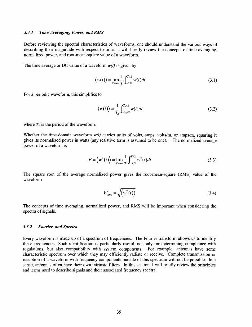
3.3.1 Time Averaging, Power, and RMS
Before reviewing the spectral characteristics of waveforms, one should understand the various ways ofdescribing their magnitude with respect to time. I will briefly review the concepts of time averaging,normalized power, and root-mean-square value of a waveform.
The time average or DC value of a waveform w(t) is given by
(w(t)) = lim f2 w(t)dt (3.1)T--oo T 1i-T/2
For a periodic waveform, this simplifies to
1 fTo/2(w(t))= -I w(t)dt (3.2)T f-To/2
where To is the period of the waveform.
Whether the time-domain waveform w(t) carries units of volts, amps, volts/m, or amps/m, squaring itgives its normalized power in watts (any resistive term is assumed to be one). The normalized averagepower of a waveform is
P = w2 (t))= liml-I w2 (t)dt (3.3)T-4 T f -T/2
The square root of the average normalized power gives the root-mean-square (RMS) value of thewaveform
Wrms -= W2 (t)) (3.4)
The concepts of time averaging, normalized power, and RMS will be important when considering thespectra of signals.
3.3.2 Fourier and Spectra
Every waveform is made up of a spectrum of frequencies. The Fourier transform allows us to identifythese frequencies. Such identification is particularly useful, not only for determining compliance withregulations, but also compatibility with system components. For example, antennas have somecharacteristic spectrum over which they may efficiently radiate or receive. Complete transmission orreception of a waveform with frequency components outside of this spectrum will not be possible. In asense, antennas often have their own intrinsic filters. In this section, I will briefly review the principlesand terms used to describe signals and their associated frequency spectra.
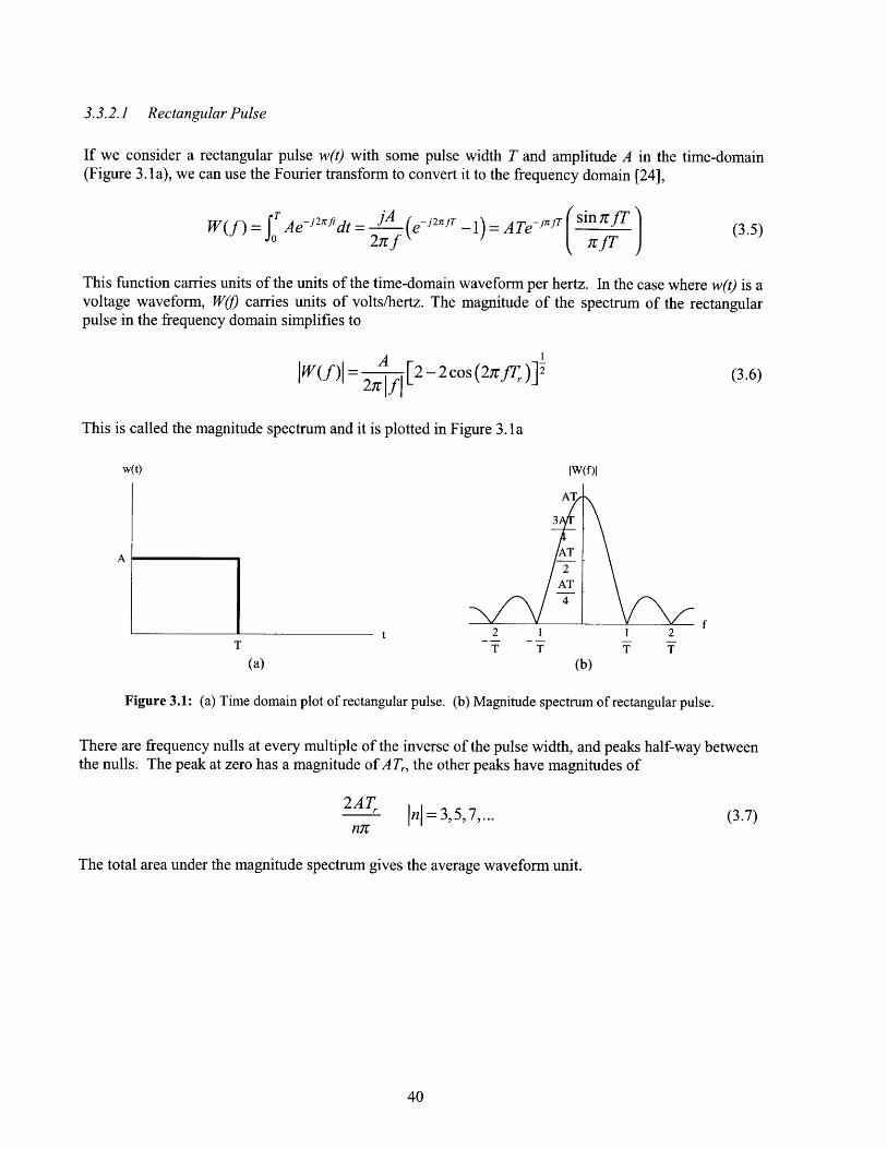
3.3.2.1 Rectangular Pulse
If we consider a rectangular pulse w(t) with some pulse width T and amplitude A in the time-domain(Figure 3.1 a), we can use the Fourier transform to convert it to the frequency domain [24],
W() = rAe-j2tldt = j A (ej 2Zrf -1) = ATe-JII sin 7rfTW(f) 2f / ifT
This function carries units of the units of the time-domain waveform per hertz. In the case where w(t) is avoltage waveform, W(1) carries units of volts/hertz. The magnitude of the spectrum of the rectangularpulse in the frequency domain simplifies to
W(f) = 2A [2-2 cos (27rJT )]2Ir2(rl - I (3.6)
This is called the magnitude spectrum and it is plotted in Figure 3.1 a
IW(f)l
T T T T
Figure 3.1: (a) Time domain plot of rectangular pulse. (b) Magnitude spectrum of rectangular pulse.
There are frequency nulls at every multiple of the inverse of the pulse width, and peaks half-way betweenthe nulls. The peak at zero has a magnitude of AT,, the other peaks have magnitudes of
2AT,
n7Cjnl = 3,5,7,... (3.7)
The total area under the magnitude spectrum gives the average waveform unit.
w(t)
(3.5)
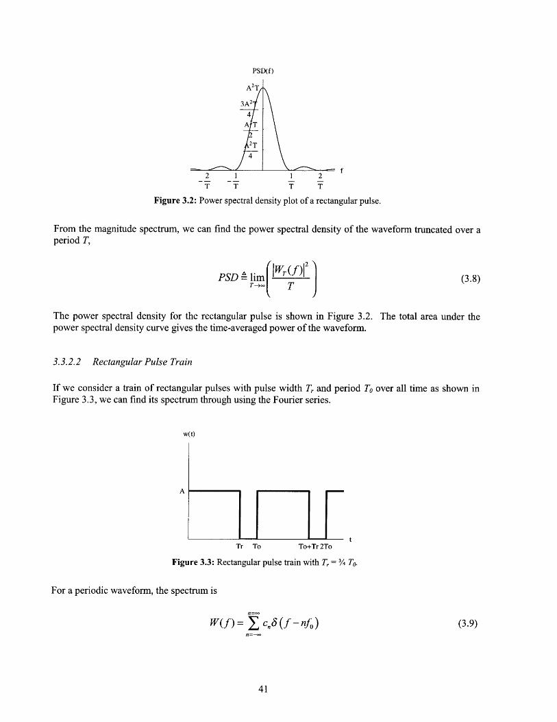
PSD(f)
2 1 1 2
T T T T
Figure 3.2: Power spectral density plot of a rectangular pulse.
From the magnitude spectrum, we can find the power spectral density of the waveform truncated over aperiod T,
PSD --m i (3.8)
The power spectral density for the rectangular pulse is shown in Figure 3.2. The total area under thepower spectral density curve gives the time-averaged power of the waveform.
3.3.2.2 Rectangular Pulse Train
If we consider a train of rectangular pulses with pulse width Tr and period To over all time as shown inFigure 3.3, we can find its spectrum through using the Fourier series.
w(t)
Tr To
HrFigure 3.3: Rectangular pulse train with Tr = ¾ To.
For a periodic waveform, the spectrum is
n=oow(f) =Y, c, (f - nfo)
n=-oo
To+Tr2To
(3.9)
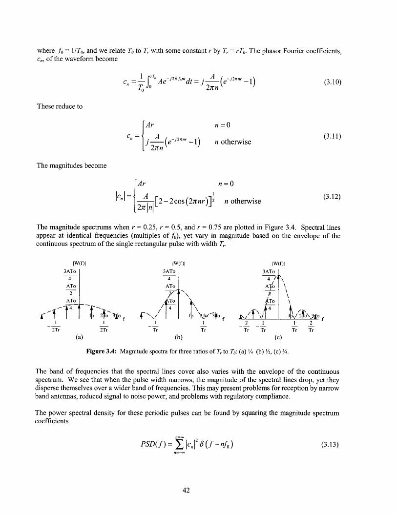
where fo = 1/To, and we relate To to T,r with some constant r by Tr = rTo. The phasor Fourier coefficients,cn, of the waveform become
(3.10)cn = •1 O Ae-j2Kfontdt = jA (·j2nrn T fo A2- (en
These reduce to
ArC = A (ej2nr
2n(e -1)
n = 0
n otherwise
The magnitudes become
Ar n=0O
cni = A [ (3.12)2n [A2-2cos(2rnr)]2 n otherwise (3.12)
The magnitude spectrums when r = 0.25, r = 0.5, and r = 0.75 are plotted in Figure 3.4. Spectral linesappear at identical frequencies (multiples of fo), yet vary in magnitude based on the envelope of thecontinuous spectrum of the single rectangular pulse with width Tr.
jwl3ATo
4ATo
2
ATo
rI m:?
IW(f)I3ATo
ATo
T4•.. //
1T2Tr
Figure 3.4: Magnitude spectra for three ratios of Tr to To: (a) 1/4 (b) /2, (c) 3/4.
The band of frequencies that the spectral lines cover also varies with the envelope of the continuousspectrum. We see that when the pulse width narrows, the magnitude of the spectral lines drop, yet theydisperse themselves over a wider band of frequencies. This may present problems for reception by narrowband antennas, reduced signal to noise power, and problems with regulatory compliance.
The power spectral density for these periodic pulses can be found by squaring the magnitude spectrumcoefficients.
(3.13)
(3.11)
IW(f)I3ATo
4 /i
A o
\2f'r 1*o
\To
2 1
Tr Tr
tb/ 'C\,3f
1 2
Tr Tr
n=-
PSD(f) = C lc n [2 4 (f- nf o)n=-
f t1
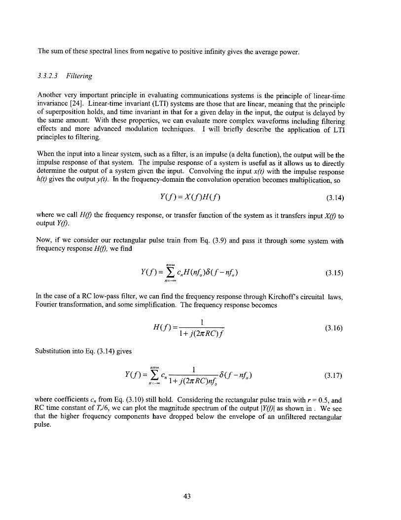
The sum of these spectral lines from negative to positive infinity gives the average power.
3.3.2.3 Filtering
Another very important principle in evaluating communications systems is the principle of linear-timeinvariance [24]. Linear-time invariant (LTI) systems are those that are linear, meaning that the principleof superposition holds, and time invariant in that for a given delay in the input, the output is delayed bythe same amount. With these properties, we can evaluate more complex waveforms including filteringeffects and more advanced modulation techniques. I will briefly describe the application of LTIprinciples to filtering.
When the input into a linear system, such as a filter, is an impulse (a delta function), the output will be theimpulse response of that system. The impulse response of a system is useful as it allows us to directlydetermine the output of a system given the input. Convolving the input x(t) with the impulse responseh(t) gives the output y(t). In the frequency-domain the convolution operation becomes multiplication, so
Y(f) = X(f)H(f) (3.14)
where we call H(f) the frequency response, or transfer function of the system as it transfers input X(/) tooutput Y(f).
Now, if we consider our rectangular pulse train from Eq. (3.9) and pass it through some system withfrequency response H(f), we find
Y(f)= cH(nfo)5(f-nfo) (3.15)n=-oo
In the case of a RC low-pass filter, we can find the frequency response through Kirchoff's circuital laws,Fourier transformation, and some simplification. The frequency response becomes
H(f) = (3.16)1 + j(21rRC)f
Substitution into Eq. (3.14) gives
Y(f)= c, 5 (f - nfo) (3.17)n=- 1+ j(27cRC)nfo
where coefficients cn from Eq. (3.10) still hold. Considering the rectangular pulse train with r = 0.5, andRC time constant of Tr/6, we can plot the magnitude spectrum of the output Y(f)1 as shown in . We seethat the higher frequency components have dropped below the envelope of an unfiltered rectangularpulse.
____
IW(f)I
3ATo
4
ATo
/
SATo/ 4
Tr To To+Tr 2To1
Tr
Figure 3.5: Low-pass filtered rectangular pulse: (a) waveform (b) magnitude spectrum.
3.3.2.4 Modulation
The signals we have considered thus far have been baseband signals in that their spectra have beencentered around zero frequency. When transmitting information over wireless channels it is most oftennecessary to map the baseband signal onto a carrier signal through modulation. This creates a bandpasssignal with spectra centered around the carrier frequency.
Though I will discuss modulation in a subsequent section, it is useful to examine the general spectralcharacteristics of a modulated waveform. For a general baseband waveform g(t), the modulated bandpasssignal with carrier frequency coc is [24]
v(t) = Re{g(t)ejO• )= g(t)cos (cot) (3.18)
The spectrum is
V(f)= l[G(f - f)+ G*(-f - f)] (3.19)
and the PSD is
PSD(f) = [PSD, (f - f) + PSD,(-f - f)] (3.20)
We notice that the act of modulation centers the spectrum of the baseband waveform around both thepositive and negative carrier frequency while halving the magnitudes of each. As we would expect thereis a similar effect on the power spectral density.
3.3.2.5 Bandwidth
The concept of bandwidth is of particular importance from the standpoint of data rates, signal powerrelative to noise power, and regulatory compliance. In general, bandwidth refers to the range of positive
A
\X
__1____
w(t)
frequencies that a signal occupies, but there is no single formal definition. I will give definitions of sometypes we will encounter in further discussions [24]:
- Absolute bandwidth is the range of frequencies outside of which the magnitude spectrum is zero.- N-dB bandwidth, where n is some value, typically 3, 20, or 60, is the range of frequencies where the
magnitude spectra fall no lower than n-dB below the maximum value.- Null-to-null bandwidth for bandpass systems is the range of frequencies from the first null above and
below the center frequency. For baseband systems it is typically from 0 to the first null frequency.
When discussing signals on relative terms, it may not be necessary to specify the type of bandwidth.However, when discussing signals on absolute terms, the type of bandwidth should be specified.
3.4 Line Coding
In digital communications systems, digital data symbols must be converted into some transmittable form.This is typically done by sending trains of pulses that are formatted to represent the data symbols. Thispulse formatting is often called line coding. I will briefly discuss line coding in the context of wirelesstransmission and RFID.
Line coding originated in telephony, where transmission was over a copper wire line [25]. It applies,however, to wireless transmission as well. Figure 3.6 shows a number of the more common codingtechniques. Depending on implementation, there may be two or three levels - positive and zero, orpositive, negative, and zero. Those signals using both positive and negative levels are referred to asbipolar or polar, while those using only positive and zero are referred to as unipolar. Because line codingis used in wired baseband transmission, these levels have significant meanings. As RFID systemstransmit bandpass signals, however, the coded pulse train will be modulated onto a carrier. Depending onthe modulation scheme used, it may be necessary to convert a bipolar scheme to a unipolar scheme, as isthe case with amplitude shift key. Because coding and modulation together determine bandwidth,probability of error, and receiver complexity, I will save much analysis until I discuss modulation. I willhowever, derive and plot the power spectral densities of the coding schemes of interest.
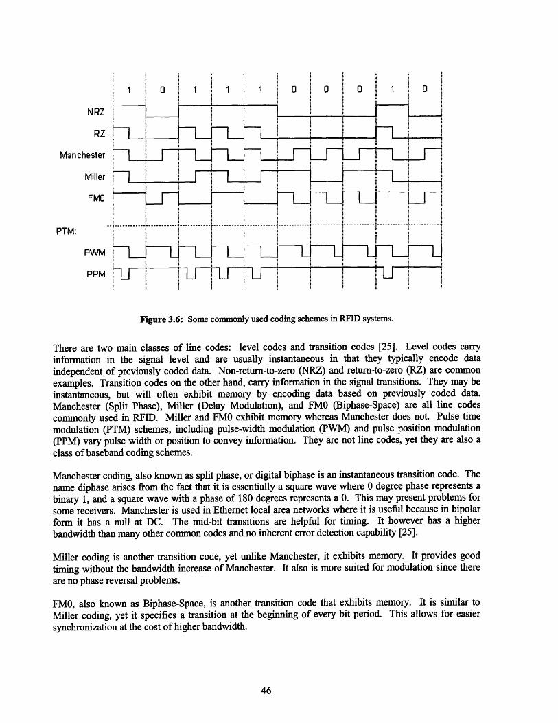
I1I 1i
PPM F1j
0 INRZ
RZ
Man chester
Miller
FMO
PTM:
PWM
1
K
SI71-
..
17
1
-F-7
............ .
--I_-LF
0
---
-T_
0
-I--
0
~FLLJ7LffiK
T........... o. K
Figure 3.6: Some commonly used coding schemes in RFID systems.
There are two main classes of line codes: level codes and transition codes [25]. Level codes carryinformation in the signal level and are usually instantaneous in that they typically encode dataindependent of previously coded data. Non-return-to-zero (NRZ) and return-to-zero (RZ) are commonexamples. Transition codes on the other hand, carry information in the signal transitions. They may beinstantaneous, but will often exhibit memory by encoding data based on previously coded data.Manchester (Split Phase), Miller (Delay Modulation), and FMO (Biphase-Space) are all line codescommonly used in RFID. Miller and FMO exhibit memory whereas Manchester does not. Pulse timemodulation (PTM) schemes, including pulse-width modulation (PWM) and pulse position modulation(PPM) vary pulse width or position to convey information. They are not line codes, yet they are also aclass of baseband coding schemes.
Manchester coding, also known as split phase, or digital biphase is an instantaneous transition code. Thename diphase arises from the fact that it is essentially a square wave where 0 degree phase represents abinary 1, and a square wave with a phase of 180 degrees represents a 0. This may present problems forsome receivers. Manchester is used in Ethernet local area networks where it is useful because in bipolarform it has a null at DC. The mid-bit transitions are helpful for timing. It however has a higherbandwidth than many other common codes and no inherent error detection capability [25].
Miller coding is another transition code, yet unlike Manchester, it exhibits memory. It provides goodtiming without the bandwidth increase of Manchester. It also is more suited for modulation since thereare no phase reversal problems.
FMO, also known as Biphase-Space, is another transition code that exhibits memory. It is similar toMiller coding, yet it specifies a transition at the beginning of every bit period. This allows for easiersynchronization at the cost of higher bandwidth.
U
__ I
F-1
............. i........... i.............I
1
i
............
Pulse time modulation (PTM) is a class of coding schemes that typically encodes an analog signal ontothe time scale of a digital signal [24]. It includes pulse width modulation (PWM) and pulse positionmodulation (PPM). It is often used in RFID systems by encoding digital signals onto the time scale of atransmission. In pulse position modulation, a modulation for some interval within a frame mightrepresent a 1 while no modulation might represent a 0. In pulse width modulation, binary is and Oswould each be assigned different pulse widths defined from a common edge. Such schemes can bebeneficial from the standpoint of bandwidth, synchronization, and probability of error.
These are only some commonly used codes, most of which were designed for wired systems. As thetransmission, channel, and reception is much different for wireless systems, it may be advantageous todefine a coding scheme unique to the application. Pulse time modulation schemes, in general, allow thisflexibility. I will analyze these various coding schemes in combination with modulation in the nextsection.
3.4.1 Baseband Power Spectral Densities
Though the coded signal will ultimately modulate a carrier, it is still useful to examine its basebandspectral characteristics. Depending on the modulation scheme used, the spectral characteristics will likelyremain the same, only the spectrum will be centered around the carrier frequency and decreased inmagnitude as described by Eq. (3.19). As mentioned, many of these coding schemes were originallydesigned for bipolar operation. Consequently most analyses of their spectral characteristics are based ontheir unipolar form. For reasons outlined in Section 3.4, I will derive their power spectral densities inunipolar form.
There are two approaches to computing the power spectral density of a signal - deterministic methods andprobabilistic methods. Deterministic methods, as those presented in Section 3.2.2, require priorknowledge of the exact waveform. Probabilistic methods, however, assign probabilities to certainelementary waveforms of which the signal is composed. As I will assume a random signal, probabilisticmethods are appropriate.
Often a random process, in our case, a signal, will have some special structure that allows it to becharacterized with relatively few specifications. The Markov process is one of these special processes.Markov processes describe random processes where the future state depends only on the present state andnot on the past history. This is true, in general, of the coded signals we will consider. When composed ofdiscrete states, a Markov process is called a Markov chain [26].
Following the approach of [27] based on [28] we will consider a Markov signal composed of Nelementary waveforms of the set {si(t); i = 1, 2, ... , N} with common period T,. A signal's sequence ischaracterized by a set of stationary probabilities {pi; i = 1, 2, ... , N} and a set of transition probabilities{Pik; i = 1, 2, ... , N }. Stationary probabilities indicate the probability of a particular elementarywaveform occurring, while transition probabilities indicate the probability of waveform sk followingwaveform si. Formally, transition probabilities are defined by
Pik = P{S,,b = k s,n = i} i 2 1,k 2b 1 (3.21)
They can be arranged in a transition probability matrix P defined by
__ ______ ____b
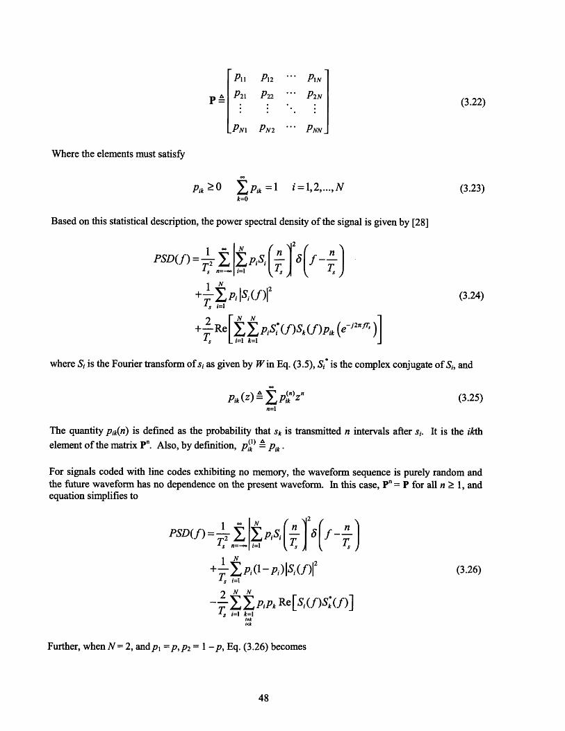
P11 P12 PIN
P 21 P22 P2N (3.22)
PNI PN2 "' PNN
Where the elements must satisfy
pik 0 pik =1 i=1,2,...,N (3.23)k=0
Based on this statistical description, the power spectral density of the signal is given by [28]
PSD(f) = - - p , f - n
s i=1
+---Re S(f)Sk (f)Pik (e - 2 )]Ts i=1 k=l1
where Si is the Fourier transform of si as given by W in Eq. (3.5), Si* is the complex conjugate of Si, and
Pik (Z) ,n)k (3.25)n=1
The quantity pik(n) is defined as the probability that sk is transmitted n intervals after si. It is the ikthelement of the matrix P". Also, by definition, pi) - Pik
For signals coded with line codes exhibiting no memory, the waveform sequence is purely random andthe future waveform has no dependence on the present waveform. In this case, pn= P for all n 2 1, andequation simplifies to
PSD(f) = pS, 2
1N+_y- p (1- Pi) IS (sf)12 (3.26)
Ts i=12N N
XY ,pPk Re[S,(f)S(f)]TS i=1 k=1ikFurther, when N = 1 -p, Eq. (3.26) becomes
Further, when N= 2, and p, =p, P2 = 1 - p, Eq. (3.26) becomes
_ ___ __ _
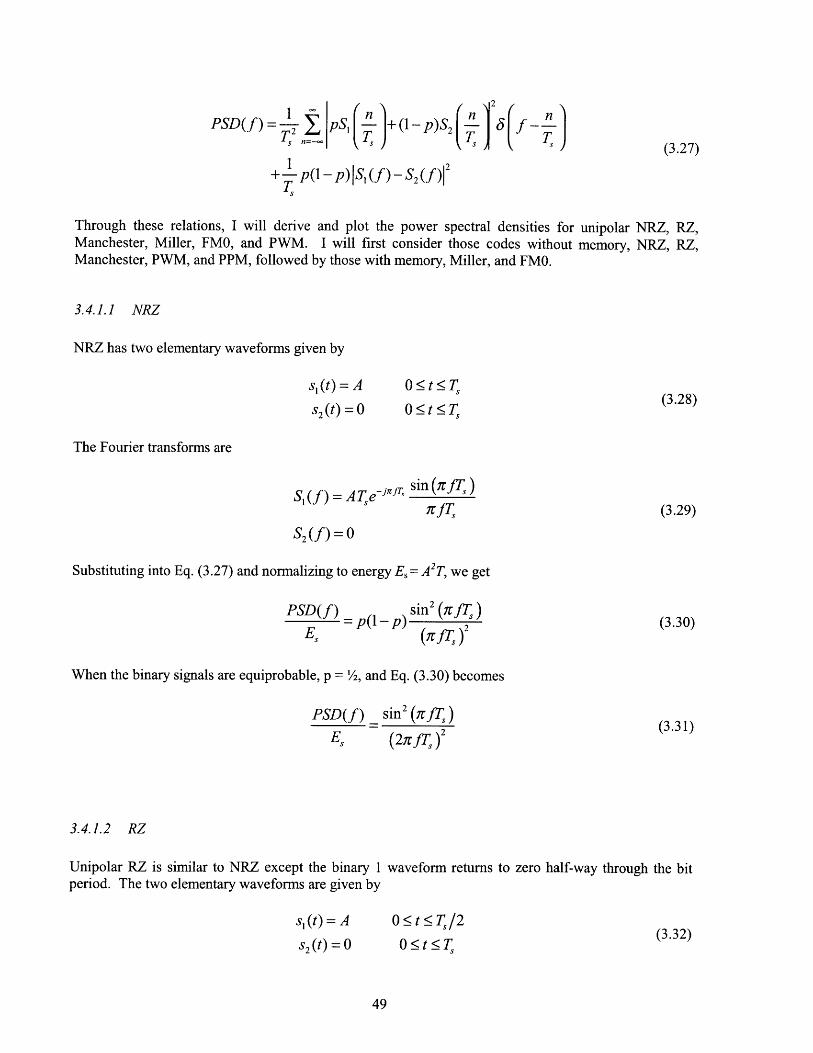
PSD(f)= pST, + (1- p)S21,ný (T T(3.27)
+ 1 p(1- p)S (f)- S2 (f)12
T
Through these relations, I will derive and plot the power spectral densities for unipolar NRZ, RZ,Manchester, Miller, FMO, and PWM. I will first consider those codes without memory, NRZ, RZ,Manchester, PWM, and PPM, followed by those with memory, Miller, and FMO.
3.4.1.1 NRZ
NRZ has two elementary waveforms given by
s1 (t) = A
s2(t) =0
The Fourier transforms are
0• t T,
0• t T,(3.28)
(3.29)S, (f) = ATe-j'm' sin (ZJTs)
irJT)
S2(f) =0
Substituting into Eq. (3.27) and normalizing to energy E, = A2T, we get
PSD(f) sin 2 (IrJTA)= P(1- p) 2
When the binary signals are equiprobable, p = 2, and Eq. (3.30) 2
When the binary signals are equiprobable, p = 'A, and Eq. (3.30) becomes
PSD(f)
Es
(3.30)
(3.31)sin 2 (rfJT)
(2 fJTs )2
3.4.1.2 RZ
Unipolar RZ is similar to NRZ except the binary 1period. The two elementary waveforms are given by
s, (t) = A
s2(t) = 0
waveform returns to zero half-way through the bit
SO t Ts /2
O<t<T (3.32)""
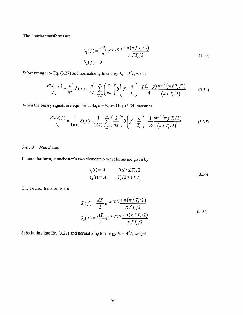
The Fourier transforms are
ATs -jf,/ 2 sin (rf Ts/2)S,(f) = s e s /2
2 rfT77/2
S2(f)=0
Substituting into Eq. (3.27) and normalizing to energy Es = A2T, we get
PSD(f) p (f)+ 2 2
E, 4 Ts T, ,n= n 4
2 jin + p(l- p) sinZ (2rJf Ts/2 )
T, 4 (rf T,/2)2
When the binary signals are equiprobable, p = /2, and Eq. (3.34) becomes
1=- (f)
16T,1 6T2
1 sin 2 ( srfT,/2)
16 (-f T,/2)2
3.4.1.3 Manchester
In unipolar form, Manchester's two elementary waveforms are given by
s, (t) = A
s2 (t) = A•O t Ts/2
T /2• t < Ts
The Fourier transforms are
AT -jirf ,/2 sin(rf T,/2)S, (f) =- e
2 7rf Ts/2
AT -j3fTsr /2 sin (rf T/2)S2(f) e/2
2 irf T/2
Substituting into Eq. (3.27) and normalizing to energy E, = A2T, we get
(3.33)
PSD(f)
Es
(3.34)
(3.35)
(3.36)
(3.37)
__ ___ ~ _______~
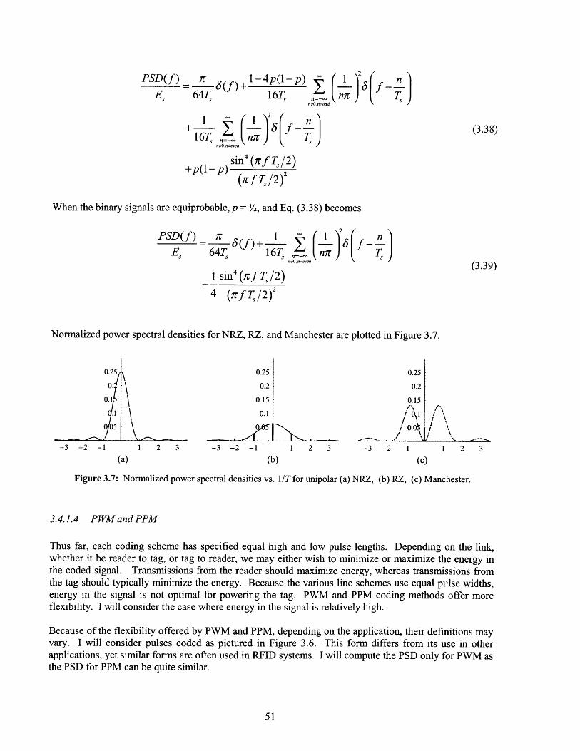
PSD( f) ir- 64 (f)
E, 64T,+ -4p(l -p) -1 2nn
16T, nn Td
1 1 n16Ts =._ n-' T,
sin 4 (isf Ts / 2)+p(1 - p)
(ivf Ts/2)2
When the binary signals are equiprobable, p = ½2, and Eq. (3.38) becomes
PSD(f) iE (f)
E, 64T,
(3.38)
1 C- 11 n+ I f16T n1r Tfn*On1ve(3.39)
1 sin 4 (irfTs/2)
4 (irf Ts2)2
Normalized power spectral densities for NRZ, RZ, and Manchester are plotted in Figure 3.7.
0.25
0.
0.1011
0-- 005
-3 -2 -1
0.25
0.2
0.15
0.1
1 2 3 -3 -2 -1
0.25
0.2
1 2 3 -3 -2 -1 1 2 3
Figure 3.7: Normalized power spectral densities vs. 1/T for unipolar (a) NRZ, (b) RZ, (c) Manchester.
3.4.1.4 PWM and PPM
Thus far, each coding scheme has specified equal high and low pulse lengths. Depending on the link,whether it be reader to tag, or tag to reader, we may either wish to minimize or maximize the energy inthe coded signal. Transmissions from the reader should maximize energy, whereas transmissions fromthe tag should typically minimize the energy. Because the various line schemes use equal pulse widths,energy in the signal is not optimal for powering the tag. PWM and PPM coding methods offer moreflexibility. I will consider the case where energy in the signal is relatively high.
Because of the flexibility offered by PWM and PPM, depending on the application, their definitions mayvary. I will consider pulses coded as pictured in Figure 3.6. This form differs from its use in otherapplications, yet similar forms are often used in RFID systems. I will compute the PSD only for PWM asthe PSD for PPM can be quite similar.
. . . . .· I . . . . .. II , , • . .
We can find the power spectral density of a pulse width modulated signal with pulse width T, = rlT,representing a logic 1, and T2 = r2 Ts representing a logic 0. The signal is composed of two separatesignals s, and s2, with probabilities of occurrence pi = p and p2 = l-p, respectively.
A 0 :5, T &t T,S2(t) A 0!5tT 2s2( (3.40)
0 T2 0 t <_T,
Taking the Fourier transform of these rectangular pulses, we get
S, (f) = ArTe-i j r sin (QrfriT)r frT (3.41)
S2(f) = Ar2Tse - j fr2 sin (7rfr2T)7rfr2T
Substituting into Eq. (3.27) and normalizing to energy E, = A2T, we get
PSD( f) _ [P(ri -r2) +r2ps 8f)E, 2T2
1 1- p(1-p)-pcos(2inrt)+ p(1-p)cos[2xn(r -r2)]-(-p)cos(2nr2) (3.42
T, n 2(nF)
sin2 [XJf/ (rl -r2)]+p(1-p) 2
When the binary signals are equiprobable, p = /2, and Eq. (3.42) becomes
PSD(f) (r -r2)+ 2 (f)
E, 2Ts,1 3-2cos(2nr)+ cos [2n (r -r2) -2cos(2nr2) (3.43)
+-2 (3.43)T, =- 8 (Tn)1 sin2 [rJTQ (rI - r)]
4 (Jf/T )2
Arbitrarily setting ri = 1/2 and r2 = 7/8, Eq. (3.43) becomes,
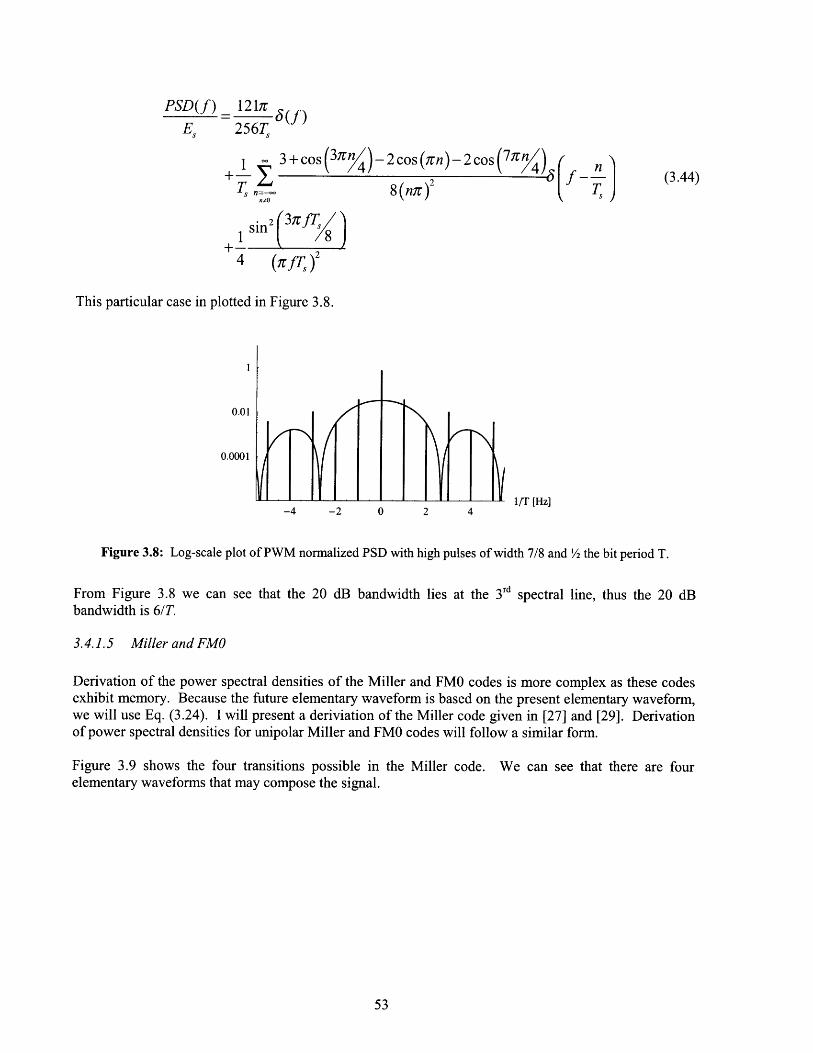
PSD(f) 121nEs 256T,
S 3+cos (3xr 4)-2cos(rn)- 2cos 7 r4) n
T n=- 8 (n Tn
1 sin2 31rfT/+-
4 (I fTs)2
This particular case in plotted in Figure 3.8.
0.01
0.0001
(3.44)
KIVi-4 -2 0 2 4
1/T [Hz]
Figure 3.8: Log-scale plot of PWM normalized PSD with high pulses of width 7/8 and '/2 the bit period T.
From Figure 3.8 we can see that the 20 dB bandwidth lies at the 3rd spectral line, thus the 20 dBbandwidth is 6/T.
3.4.1.5 Miller and FMO
Derivation of the power spectral densities of the Miller and FMO codes is more complex as these codesexhibit memory. Because the future elementary waveform is based on the present elementary waveform,we will use Eq. (3.24). I will present a deriviation of the Miller code given in [27] and [29]. Derivationof power spectral densities for unipolar Miller and FMO codes will follow a similar form.
Figure 3.9 shows the four transitions possible in the Miller code. We can see that there are fourelementary waveforms that may compose the signal.
t
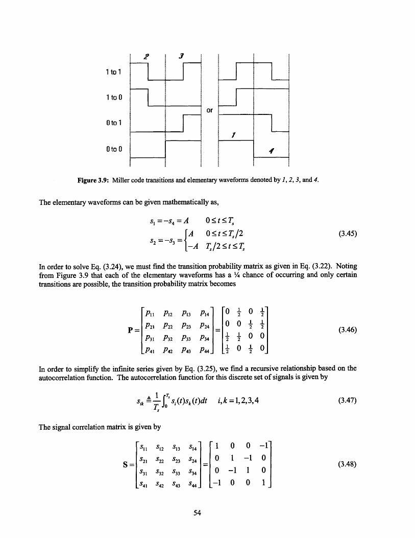
2 3
1 to 1
1 to 0
Oto 1
Oto 0
rL
Figure 3.9: Miller code transitions and elementary waveforms denoted by 1, 2, 3, and 4.
The elementary waveforms can be given mathematically as,
S1 = -S4 = A O<t<T
JA 0 • t< Ts1/2s2 =-s3 A Tl/2 5 t < Ts
(3.45)
In order to solve Eq. (3.24), we must find the transition probability matrix as given in Eq. (3.22). Notingfrom Figure 3.9 that each of the elementary waveforms has a /4 chance of occurring and only certaintransitions are possible, the transition probability matrix becomes
PiH P12 P13 P14 0 1 0 2
S P21 p22 P23 p24 10 0 YP31 P32 P33 P34 0 0
[P 41 P42 P43 P44 2 O] 0 0
(3.46)
In order to simplify the infinite series given by Eq. (3.25), we find a recursive relationship based on theautocorrelation function. The autocorrelation function for this discrete set of signals is given by
Sik •o S, (t)sk(t)dt i,k =1,2,3,4 (3.47)
The signal correlation matrix is given by
Sl1 S12 S13 S14 1 0 0 -1]
S 21 S22 S23 S24 0 1 -1 0 (3.48)S -(3.48)
S31 S32 S33 S34 0 -1 1 0
S41 S42 S43 S44 -1 0 0 1
i
-L
,,~
3
~ L
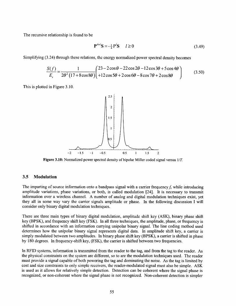
The recursive relationship is found to be
p4+1S = - PtS 1 0 (3.49)
Simplifying (3.24) through these relations, the energy normalized power spectral density becomes
S(f) 1 23-2 cos- 22 cos 20 -12 cos 3 + 5 cos 4 (3.50)E, 202 (17+8cos80) +12cos50+2cos 6 -8cos70+2cos8 (3.50)
This is plotted in Figure 3.10.
-2 -1.5 -1 -0.5 0.5 1 1.5 2
Figure 3.10: Normalized power spectral density of bipolar Miller coded signal versus 1/T.
3.5 Modulation
The imparting of source information onto a bandpass signal with a carrier frequencyfc while introducingamplitude variations, phase variations, or both, is called modulation [24]. It is necessary to transmitinformation over a wireless channel. A number of analog and digital modulation techniques exist, yetthey all in some way vary the carrier signals amplitude or phase. In the following discussion I willconsider only binary digital modulation techniques.
There are three main types of binary digital modulation, amplitude shift key (ASK), binary phase shiftkey (BPSK), and frequency shift key (FSK). In all three techniques, the amplitude, phase, or frequency isshifted in accordance with an information carrying unipolar binary signal. The line coding method useddetermines how the unipolar binary signal represents digital data. In amplitude shift key, a carrier issimply modulated between two amplitudes. In binary phase shift key (BPSK), a carrier is shifted in phaseby 180 degrees. In frequency-shift key, (FSK), the carrier is shifted between two frequencies.
In RFID systems, information is transmitted from the reader to the tag, and from the tag to the reader. Asthe physical constraints on the system are different, so to are the modulation techniques used. The readermust provide a signal capable of both powering the tag and dominating the noise. As the tag is limited bycost and size constraints to only simple receivers, the reader-modulated signal must also be simple. ASKis used as it allows for relatively simple detection. Detection can be coherent where the signal phase isrecognized, or non-coherent where the signal phase is not recognized. Non-coherent detection is simpler
_ __ _ _
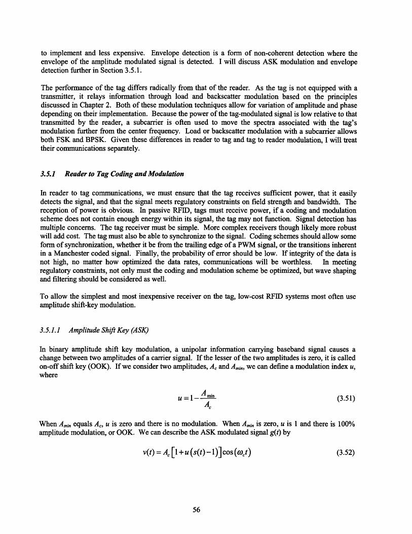
to implement and less expensive. Envelope detection is a form of non-coherent detection where theenvelope of the amplitude modulated signal is detected. I will discuss ASK modulation and envelopedetection further in Section 3.5.1.
The performance of the tag differs radically from that of the reader. As the tag is not equipped with atransmitter, it relays information through load and backscatter modulation based on the principlesdiscussed in Chapter 2. Both of these modulation techniques allow for variation of amplitude and phasedepending on their implementation. Because the power of the tag-modulated signal is low relative to thattransmitted by the reader, a subcarrier is often used to move the spectra associated with the tag'smodulation further from the center frequency. Load or backscatter modulation with a subcarrier allowsboth FSK and BPSK. Given these differences in reader to tag and tag to reader modulation, I will treattheir communications separately.
3.5.1 Reader to Tag Coding and Modulation
In reader to tag communications, we must ensure that the tag receives sufficient power, that it easilydetects the signal, and that the signal meets regulatory constraints on field strength and bandwidth. Thereception of power is obvious. In passive RFID, tags must receive power, if a coding and modulationscheme does not contain enough energy within its signal, the tag may not function. Signal detection hasmultiple concerns. The tag receiver must be simple. More complex receivers though likely more robustwill add cost. The tag must also be able to synchronize to the signal. Coding schemes should allow someform of synchronization, whether it be from the trailing edge of a PWM signal, or the transitions inherentin a Manchester coded signal. Finally, the probability of error should be low. If integrity of the data isnot high, no matter how optimized the data rates, communications will be worthless. In meetingregulatory constraints, not only must the coding and modulation scheme be optimized, but wave shapingand filtering should be considered as well.
To allow the simplest and most inexpensive receiver on the tag, low-cost RFID systems most often useamplitude shift-key modulation.
3.5.1.1 Amplitude Shift Key (ASK)
In binary amplitude shift key modulation, a unipolar information carrying baseband signal causes achange between two amplitudes of a carrier signal. If the lesser of the two amplitudes is zero, it is calledon-off shift key (OOK). If we consider two amplitudes, Ac and Amin, we can define a modulation index u,where
u = 1 ,m•n (3.51)
When Amin equals Ac, u is zero and there is no modulation. When Amin, is zero, u is 1 and there is 100%amplitude modulation, or OOK. We can describe the ASK modulated signal g(t) by
v(t) = Ac [1 + u (s(t) -1)]cos (cot) (3.52)
__ __
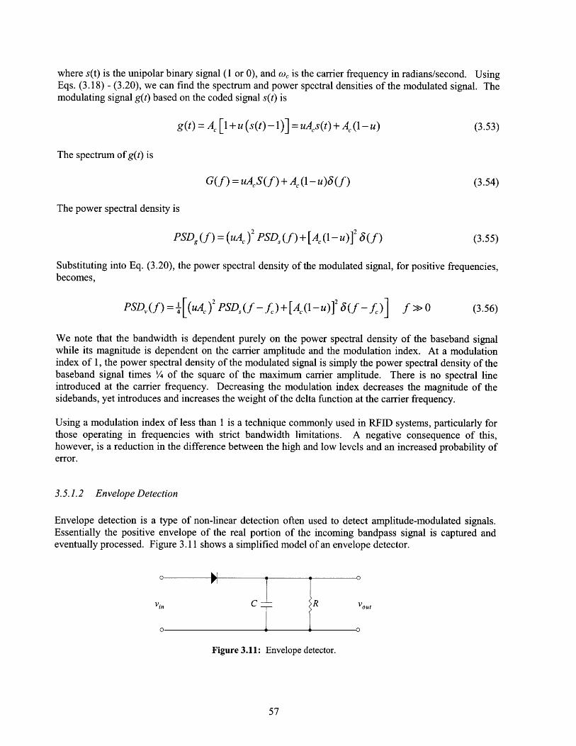
where s(t) is the unipolar binary signal (1 or 0), and wc is the carrier frequency in radians/second. UsingEqs. (3.18) - (3.20), we can find the spectrum and power spectral densities of the modulated signal. Themodulating signal g(t) based on the coded signal s(t) is
g(t) = A, [1 + u (s(t)- 1)] = uAcs(t) + A(1- u) (3.53)
The spectrum of g(t) is
G(f) = uAcS(f) + Ac (1- u)J(f) (3.54)
The power spectral density is
PSDg(f) = (uAc)2 PSD, (f) + [A(1-u)]2 6(f) (3.55)
Substituting into Eq. (3.20), the power spectral density of the modulated signal, for positive frequencies,becomes,
PSDv(f)= [(uAc)2 PSD,(f -f)+[Ac(1-u)]2 (f -f)] f> 0 (3.56)
We note that the bandwidth is dependent purely on the power spectral density of the baseband signalwhile its magnitude is dependent on the carrier amplitude and the modulation index. At a modulationindex of 1, the power spectral density of the modulated signal is simply the power spectral density of thebaseband signal times 1/4 of the square of the maximum carrier amplitude. There is no spectral lineintroduced at the carrier frequency. Decreasing the modulation index decreases the magnitude of thesidebands, yet introduces and increases the weight of the delta function at the carrier frequency.
Using a modulation index of less than 1 is a technique commonly used in RFID systems, particularly forthose operating in frequencies with strict bandwidth limitations. A negative consequence of this,however, is a reduction in the difference between the high and low levels and an increased probability oferror.
3.5.1.2 Envelope Detection
Envelope detection is a type of non-linear detection often used to detect amplitude-modulated signals.Essentially the positive envelope of the real portion of the incoming bandpass signal is captured andeventually processed. Figure 3.11 shows a simplified model of an envelope detector.
Figure 3.11: Envelope detector.
_ __ _ ___ ___
The resistor and capacitor form a low-pass filter where the time constant is set so that the output signalfollows the signal envelope. The upper bounds of the low-pass filter should be much less than the carrierfrequency, but much larger than the bandwidth of the incoming modulated signal [24].
1B << < fe (3.57)
27rRC
The envelope detector output is essentially the envelope of the incoming signal multiplied by aproportionality constant K. For the envelope of the ASK modulated signal from Eq. (3.53), the outputvoltage is given as
v0o, (t) = K g(t)[ = KuAcs(t) + KAc (1- u) (3.58)
One should note that a DC value exists for modulation indices of less than 1.
3.5.2 Tag to Reader Modulation and Coding
In the tag to reader link, conditions and requirements are somewhat different from the reader to tag link.The tag communicates through either load modulation or backscatter modulation. Depending on theimplementation, amplitude and phase or simply amplitude are varied. As opposed to the reader to taglink, coding schemes should be low energy and bandwidth is of much less concern. Because the signallevels are so low, they are not constrained by the stringent regulations at higher signal levels. Oneconsequence of the low signal, however, is difficulty in reception by the reader. The reader signal can faroutweigh that of the tag, so at times, detection can be difficult. For this reason, a subcarrier is oftenemployed. A subcarrier effectively allows BPSK or FSK modulation over the amplitude and phasemodulation inherent in load or backscatter modulation. I will briefly describe the theory of subcarriersand then further discuss the issues in tag to reader coding.
3.5.2.1 Subcarrier
A subcarrier is created by modulating the load or backscatter modulation at a higher frequency than thedata rate. Varying the phase or frequency of the subcarrier modulations allows BPSK or FSKmodulation, respectively. Some RFID systems, for example, those operating at 13.56 MHz, use asubcarrier of 212 kHz. This moves the sidebands associated with the tag's modulations 212 kHz aboveand below the carrier frequency of 13.56 MHz. Subcarriers are useful for isolating the tag's sidebandsfrom noise due to the readers signal and that inherent in the reader's receiver and amplifiers. Theyhowever require that the tag have a faster clock or an oscillator.
3.5.2.2 Coding
In tag to reader coding, unlike reader to tag coding, energy in the signal should be minimized. Lessenergy in the signal means more energy available to power the tag. The amplitude however should behigh enough so that the reader can detect the signal. Often Manchester, FMO or other line codingschemes are used. One problem with Manchester is that due to its effective phase variation, it canconfuse certain receivers as the 180 degree phase shifts can be ambiguous. Also, coding schemes withmid-bit transitions can either require a faster clock or a slower data rate - both negative effects.
___
3.5.3 Spread Spectrum
Beyond bandwidth and energy contained in a signal, there are other concerns in communications such asmultiple-access, anti-jamming, and interference rejection [24]. Spread spectrum (SS) modulation, byspreading signals over a bandwidth much larger than that require by the message signal, can allowmultiple-access, anti-jamming, and interference rejection. RFID systems often use spread spectrummodulation techniques at UHF and microwave frequencies. At these frequencies, regulations typicallyallow greater output powers for spread spectrum systems relative to narrow-band systems. Power isspread over a wide bandwidth, reducing the chance of harmful interference to and from other devices.
The two most common types of spread spectrum modulation are direct sequence (DS), and frequencyhopping (FH). In DS modulation, a pseudo-noise coded signal with period less than the message bitperiod is mixed with the message signal, creating an output signal with wide bandwidth. In order toretrieve the message, a receiver must de-spread the code with the same pseudo-noise sequence used totransmit the signal. In frequency hopping systems, multiple narrow-band channels at frequencies chosenfrom a pseudorandom list, are hopped between. This has the effect of averaging the power over the entirewidth of the hopping frequencies. Typically receivers in frequency hopping systems must hop with thesame pseudorandom list of frequencies in order to receive the modulated signal.
In low-cost passive RFID systems, spread spectrum is often used differently than originally intended. Inorder for a tag to achieve true DS or FH modulation it would require excessive complexity of the tagreceiver. Instead, a common strategy is to design the tag's antenna to have a bandwidth covering theentire width of the spread spectrum channel. In this way, the tag may receive all power, whether it beconfined in a narrow frequency hopping channel, or spread out over the entire width through directsequence. To achieve communications, the signals, whether they be frequency hopped or directsequenced, may still be amplitude modulated by the reader, and subsequently backscattered by the tag.This strategy is useful in RFID as regulations typically allow higher output powers for spread spectrumsystems and narrow-band systems.
3.6 Probability of Error
In general, there are two important factors important in the evaluation of a communication system -bandwidth, and performance in the presence of noise [24]. We have already considered bandwidth, nowwe will consider performance in the presence of noise. A figure of merit for this performance in analogsystems is the signal power to noise power ratio. In digital systems it is the probability of bit error, or biterror rate BER.
The BER is the probability of error arising when the system must make a decision between, in binarysystems, two signals. In ASK modulated signals, levels will be either high or low. In OOK signals, thelow will be zero. The receiver has a decision threshold above which signals will be considered high, andbelow which they will be considered low. The total probability of error or BER, is the sum of theprobability of error associated with each signal.
When detection is coherent, more information is used - not only the amplitude information, but also thephase information. When detection is non-coherent, however, only the amplitude information is used.Error performance thus decreases with non-coherent detection. RFID systems typically use non-coherentenvelope detection because it can be far simpler and more inexpensive to implement.
II
With OOK or ASK modulated signals, there will either be two signals levels. How these levels representa particular bit, depends on the coding scheme used. Regardless of the coding scheme however, if errorsare made in detecting these levels, there will be an error in the bit. Certain coding schemes mayinherently be able to detect such an error, while others may not. If not, other error detection or errorcorrection techniques may be employed. Noise in the wireless channel can take many forms. Twocommon forms are burst-noise and gaussian noise. Gaussian noise is typically that resulting frombackground radiation, thermal noise, and shot noise. In short-range device communications, particularlyin low-cost passive RFID communications, burst noise resulting from other interfering transmissions, inparticular, is most prevalent. I will consider burst noise for this reason, and gaussian noise to illustrate acalculation of the BER.
3.6.1 Burst Noise
Burst noise can be caused by interference from other sources or affects such as multipath. It can beparticularly harmful to RFID transmissions where signals can be low and detectors simple. Gilbert [30]models errors created by burst noise as a Markov chain where states can take one of two states - a goodstate where errors occur with low probability or a bad state where errors occur with a high probability.Elliott has further generalized this model [31], and others have applied it [32][33]. Burst errors can occoron single bits, or large blocks of bits.
3.6.2 Gaussian Noise
In considering the affect of additive gaussian noise, we will assume two general cases of signal levels,those that have a nonzero amplitude and those that have zero amplitude. In the presence of noise,probability density functions will vary with these two levels. More generally, they will vary with anyvariation in level. The simpler case is when the signal level is zero and noise is the only receivedcomponent. In OOK, this will occur. In ASK, however, with a modulation index less than 1, it will notoccur. I will describe the differences seen in probability density functions for these variations in signallevels.
First we consider the case where the transmitted signal amplitude is zero. Thus, the input c to an envelopedetector, is simply equivalent to the noise n. If we assume noise is gaussian, we can decompose it into anin-phase and quadrature form, represented by
c(t) = n(t) = x(t) cos(wct) - y(t) sin(coct) (3.59)
where both x and y are independent gaussian random variables. When the signal is zero, we simply musttransform these variables from Cartesian form to Polar form. This will give us an magnitude component rand a phase component 0. Because we assume envelope detection, we will only use the amplitudecomponent to find the probability density function associated with the signal.
Transforming the in-phase/quadrature noise to polar form and finding the probability density function of rand 0, and then integrating over all 0, gives the probability density function of the amplitude r alone. Thedistribution function found is called the Rayleigh distribution.
Now, we can consider the case where the transmitted signal has a nonzero amplitude, whether it be thefull amplitude, or the lower level when the modulation index is less than 1. This introduces an additional
value to the in-phase component of the received signal. This additional component can be given by v fromEq. (3.52) Now the detector input c becomes
c(t) = v(t) + n(t) = v(t) = [A [1 + u (s(t) -1)] + x(t)] cos(amt) - y(t) sin(mwt) (3.60)
This complicates the situation somewhat. Just as for the simple case with a zero signal amplitude, wetransform the cartesisan inphase/quadrature components to polar form. We find the probability densityfunction of r and 0 together, however in this case they are no longer independent. We find thatintegrating over theta presents us with an integral that can only be solved through a modified Besselfunction of the first kind and zero order [34].
The resulting distribution function is called a Rician distribution. We should note that setting the signalamplitude to zero, the probability density function becomes a Rayleigh distribution; setting the amplitudemuch greater than the noise in phase component, produces a Gaussian distribution. At points in between,it is Rician distribution.
Given the probability density functions of the two signal levels, we can find the probability of error. Asmentioned, it is simply the sum of the areas under the individual probability density functionscorresponding to errors at those two levels. This is represented as
P, = P f (r I v)dr + P f f(r v2)dr (3.61)
where P1 and P2 are the probabilities of signal 1 and 2 occurring, respectively. The quantity b is thethreshold level. In OOK modulation, the first probability density function is simply the Rayleighdistribution, and the second, the Rician distribution function. In the case of ASK with a modulation indexof less than 1, both density functions will be Rician distribution functions. Unfortunately, for Riciandistributions, we find that the integration of the Bessel function is not possible in closed form. Howeverit can be solved numerically. In general, we find that the less the difference in signal levels, the greaterthe error. In addition, the lower these levels with respect to RMS noise, the greater the BER. Thethreshold level must also be wisely chosen so as to minimize the probability of error. This of courserequires prior knowledge of the signal amplitude relative to noise, and is certain to be variable in RFIDsystems. Due to simple detectors, low signal levels, and likely relatively high BERs, it can be useful toincorporate some form of error detection or correction in the transmissions both from reader to tag and tagto reader. I will review such methods next.
3.7 Error Detection and Correction
There is an interesting tradeoff in RFID systems when considering the reader to tag and tag to readerlinks. The reader-transmitted signal is relatively strong, yet the tag is limited to very simple detectors andsignal processing. This leaves room for increased error. In the tag to reader link, the tag-transmittedsignal is relatively low. Even though the RFID reader may have far more capable and robust receiversand signal processing, due to the low signal level, errors may still be highly probable. Error detection orcorrection of some extent should be considered in both links.
Though there are exceptions, error detection and correction coding schemes require the addition of bits tothe original message. Depending on the number of bits and the method in which they are added, thesecodes may be able to correct or just simply detect errors. In general, error correction codes require morebits, and thus, though robust, are more inefficient and require more bandwidth and processing. In RFID
__ ___
systems, transmissions are relatively short and processing requirements are relatively stringent. For themost part, error detection codes are more appropriate.
Common types of error detection include parity checking, longitudinal redundancy checking (LRC), andcyclic redundancy checking (CRC) [6]. In parity checking, an extra bit is adding to a string of bits, whichindicates if there are an even or an odd number of binary 1 bits depending on implementation. Suchchecking is very simple, yet useless if there is an even number of errors within the string. Longitudinalredundancy checks require recursive exclusive OR (XOR) operations on each byte within a block of data.Results of the operation are appended to the string and transmitted. On reception, the same procedure isperformed. If the result of a check is not zero, an error has occurred. Similar to parity checking,however, multiple errors can cancel each other out. Cyclic redundancy checks are more robust, yetslightly more demanding on processing. The CRC operation provides a way of nearly uniquelyidentifying a string of bits. The larger the CRC, the more data can be reliably checked. Becausetransmissions are relatively short in RFID systems, 8-bit CRCs are commonly used.
3.8 Summary
In this Chapter we have studied the fundamentals of communications as performed by low-cost passiveRFID systems. We should note that there is flexibility in coding and modulation both from the reader tothe tag and the tag to the reader. We will see in subsequent chapters that coding and modulationinfluences more than just bandwidth and spectral density, and is influenced by more than just limitationson bandwidth and spectral density. In the next chapter we will see how regulations constrain bandwidth,and in subsequent chapters we will see how this affects the overall performance of the tag.
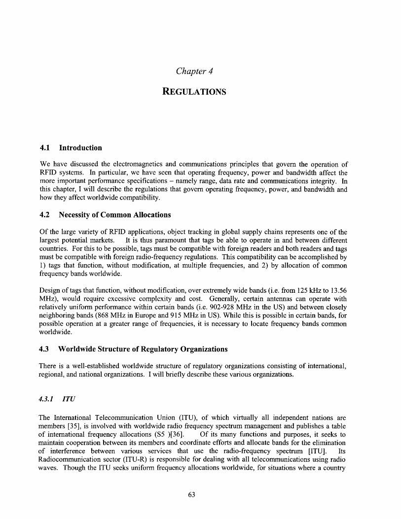
Chapter 4
REGULATIONS
4.1 Introduction
We have discussed the electromagnetics and communications principles that govern the operation ofRFID systems. In particular, we have seen that operating frequency, power and bandwidth affect themore important performance specifications - namely range, data rate and communications integrity. Inthis chapter, I will describe the regulations that govern operating frequency, power, and bandwidth andhow they affect worldwide compatibility.
4.2 Necessity of Common Allocations
Of the large variety of RFID applications, object tracking in global supply chains represents one of thelargest potential markets. It is thus paramount that tags be able to operate in and between differentcountries. For this to be possible, tags must be compatible with foreign readers and both readers and tagsmust be compatible with foreign radio-frequency regulations. This compatibility can be accomplished by1) tags that function, without modification, at multiple frequencies, and 2) by allocation of commonfrequency bands worldwide.
Design of tags that function, without modification, over extremely wide bands (i.e. from 125 kHz to 13.56MHz), would require excessive complexity and cost. Generally, certain antennas can operate withrelatively uniform performance within certain bands (i.e. 902-928 MHz in the US) and between closelyneighboring bands (868 MHz in Europe and 915 MHz in US). While this is possible in certain bands, forpossible operation at a greater range of frequencies, it is necessary to locate frequency bands commonworldwide.
4.3 Worldwide Structure of Regulatory Organizations
There is a well-established worldwide structure of regulatory organizations consisting of international,regional, and national organizations. I will briefly describe these various organizations.
4.3.1 ITU
The International Telecommunication Union (ITU), of which virtually all independent nations aremembers [35], is involved with worldwide radio frequency spectrum management and publishes a tableof international frequency allocations (S5 )[36]. Of its many functions and purposes, it seeks tomaintain cooperation between its members and coordinate efforts and allocate bands for the eliminationof interference between various services that use the radio-frequency spectrum [ITU]. ItsRadiocommunication sector (ITU-R) is responsible for dealing with all telecommunications using radiowaves. Though the ITU seeks uniform frequency allocations worldwide, for situations where a country
__ _
might require band allocations that differ from the rest of the world, exceptions are made and noted in thefrequency allocation table. For the purposes of designating region specific allocations, the ITU uses itsdivision of the world into three regions (S5.2)[36].
P- 16W1PI40' 12W~ 100" 84"~ 60`' 4tI'
•16W 104 W 1201" 1Q0W :K0o 6OPV 4W 20" 0?" -~1 0 (401 60xw u0 i0fk 120W 140Yr i •6( 184
Figure 4.4.1: ITU regions (S5.2)[36]
4.3.2 Regional/National
While the ITU fosters cooperation between and makes recommendations to regional and national bodies,it is the various regional and national bodies that set and administer the actual band allocations andemission limits. As both the world's largest economies, and largest potential markets for RFID exist inEurope, the United States, and Japan, I will focus on the standards of these countries' respectivetelecommunications standards organizations.
The European Conference of Postal and Telecommunications Administrations (CEPT) deals withsovereign and regulatory matters in the areas of post and telecommunications. Members include 43European counties including those in Central and Eastern Europe. It consists of three committees, one onpostal matters, the CERP (Comit6 europ6en des r6gulateurs postaux) and two on telecommunicationsissues: the ERC (European Radiocommuication Committee) and the ECTRA (European Committee forRegulatory Telecommunications Affairs). These committees work on harmonization issues and adoptrecommendations and decisions, normally prepared by their working groups and project teams. The ERChas established the European Radiocommunications Office (ERO), which supports the committees'activities and conducts studies for it [37].
The European Telecommunications Standards Institute (ETSI), established in 1988 by CEPT (along withCEN and CENELEC), is recognized as one of the three European Standards Organizations (ESO). It isresponsible for developing telecommunications related standards in Europe. Thirty-seven National
__
OP (F~'- 2W 40P 6t f 80&" 100~:" I_2U_ 14C" 76(*Y' 1 A
1--
Standards Organizations of thirty-four countries as far east as Russia and Turkey, provide elaboration,approval, and implementation of the standards [38].
The organizations responsible for telecommunications standards and regulations in the United States andJapan, are the Federal Communications Commission (FCC) [39], and the Ministry of Posts andTelecommunications (MPT) [40], respectively. In Japan, the Association of Radio Industries andBusinesses (ARIB) has been designated as the Center for Promotion of Efficient Use of the RadioSpectrum. Among its many tasks, ARIB develops detailed standards that fit within the less detailedrequirements of the MPT regulations [41].
4.4 Frequencies Available for RFID Use
CEPT has adopted the term "Short Range Device" (SRD) to describe "radio transmitters which provideeither unidirectional or bi-directional communication and which have low capability of causinginterference to other radio equipment." Antennas may be integral, dedicated, or external, and all types ofmodulation may be used [42]. The ITU, in their Recommendation 213/1 has supported this term andfurther recommends to national administrations that they adopt the recommended parameters and that useof SRDs should not be unnecessarily restricted. Efforts to harmonize frequency allocations worldwide areongoing.
RFID systems are considered to be short-range devices, and they may operate in certain frequency bandsallocated in most countries. I will describe these bands now.
4.4.1 ISM
In their frequency allocation tables, the ITU designates certain bands as industrial, scientific, and medical(ISM) bands. These bands are for industrial, scientific, and medical applications of radio frequencyemitting devices. Typically radiation from these devices, though often either intended, or not intended forlimited range applications, can interfere with other radio frequency communications services. For thisreason, it is necessary to allocate specific bands for their use [43]. The principal ISM bands (RRS5.150)[36] are,
13.553-13.567 MHz26.957-27.283 MHz40.66-40.70 MHz902-928 MHz (Region 2)2.4 - 2.5 GHz5.725-5.785 GHz24-24.25 GHz
Certain bands are available for ISM use only on approval of administrations that might be affected bytheir use (RR S5.138)[36],
6.765 - 6.795 MHz61.0 - 61.5 GHz122-123 GHz244-246 GHz
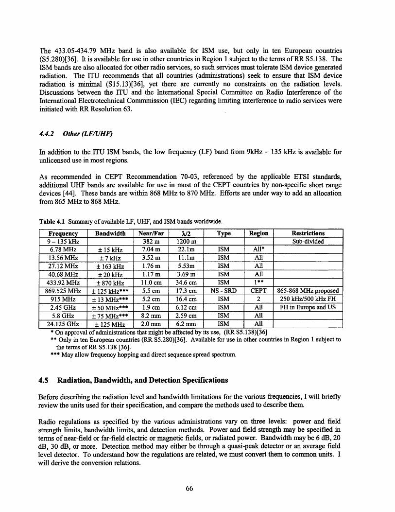
The 433.05-434.79 MHz band is also available for ISM use, but only in ten European countries(S5.280)[36]. It is available for use in other countries in Region 1 subject to the terms of RR S5.138. TheISM bands are also allocated for other radio services, so such services must tolerate ISM device generatedradiation. The ITU recommends that all countries (administrations) seek to ensure that ISM deviceradiation is minimal (S15.13)[36], yet there are currently no constraints on the radiation levels.Discussions between the ITU and the International Special Committee on Radio Interference of theInternational Electrotechnical Commmission (IEC) regarding limiting interference to radio services wereinitiated with RR Resolution 63.
4.4.2 Other (LF/UHF)
In addition to the ITU ISM bands, the low frequency (LF) band from 9kHz - 135 kHz is available forunlicensed use in most regions.
As recommended in CEPT Recommendation 70-03, referenced by the applicable ETSI standards,additional UHF bands are available for use in most of the CEPT countries by non-specific short rangedevices [44]. These bands are within 868 MHz to 870 MHz. Efforts are under way to add an allocationfrom 865 MHz to 868 MHz.
Table 4.1 Summary of available LF, UHF, and ISM bands worldwide.
Frequency Bandwidth Near/Far W/2 Type Region Restrictions9 - 135 kHz 382 m 1200 m Sub-divided
6.78 MHz + 15 kHz 7.04 m 22.1m ISM All*13.56 MHz + 7 kHz 3.52 m 11.1m ISM All27.12 MHz ± 163 kHz 1.76 m 5.53m ISM All40.68 MHz + 20 kHz 1.17 m 3.69 m ISM All
433.92 MHz + 870 kHz 11.0 cm 34.6 cm ISM 1**869.525 MHz ± 125 kHz*** 5.5 cm 17.3 cm NS - SRD CEPT 865-868 MHz proposed
915 MHz ± 13 MHz*** 5.2 cm 16.4 cm ISM 2 250 kHz/500 kHz FH2.45 GHz + 50 MHz*** 1.9 cm 6.12 cm ISM All FH in Europe and US5.8 GHz + 75 MHz*** 8.2 mm 2.59 cm ISM All
24.125 GHz ± 125 MHz 2.0 mm 6.2 mm ISM All* On approval of administrations that might be affected by its use, (RR S5.138)[36]** Only in ten European countries (RR S5.280)[36]. Available for use in other countries in Region 1 subject to
the terms of RR S5.138 [36].*** May allow frequency hopping and direct sequence spread spectrum.
4.5 Radiation, Bandwidth, and Detection Specifications
Before describing the radiation level and bandwidth limitations for the various frequencies, I will brieflyreview the units used for their specification, and compare the methods used to describe them.
Radio regulations as specified by the various administrations vary on three levels: power and fieldstrength limits, bandwidth limits, and detection methods. Power and field strength may be specified interms of near-field or far-field electric or magnetic fields, or radiated power. Bandwidth may be 6 dB, 20dB, 30 dB, or more. Detection method may either be through a quasi-peak detector or an average fieldlevel detector. To understand how the regulations are related, we must convert them to common units. Iwill derive the conversion relations.
1
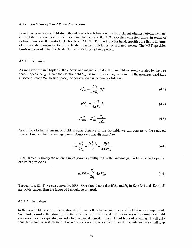
4.5.1 Field Strength and Power Conversion
In order to compare the field strength and power levels limits set by the different administrations, we mustconvert them to common units. For most frequencies, the FCC specifies emission limits in terms ofradiated power or the far-field electric field. CEPT/ETSI, on the other hand, specifies the limits in termsof the near-field magnetic field, the far-field magnetic field, or the radiated power. The MPT specifieslimits in terms of either the far-field electric field or radiated power.
4.5.1.1 Far-field
As we have seen in Chapter 2, the electric and magnetic field in the far-field are simply related by the freespace impedance rjo. Given the electric field Em, at some distance RE, we can find the magnetic field Hmaxat some distance RH. In free space, the conversion can be done as follows,
Efax = Id 0k (4.1)41RE
Id.CHff = k (4.2)
m" 4z RH
Hm x = Efff RE (4.3)m m 0RH
Given the electric or magnetic field at some distance in the far-field, we can convert to the radiatedpower. First we find the average power density at some distance REH,
E_ H2 2rG,
S i ° = _tG_ (4.4)200 2 4 RZH
EIRP, which is simply the antenna input power Pt multiplied by the antenna gain relative to isotropic G,,can be expressed as
E2EIRP = 4 rREH (4.5)
2770
Through Eq. (2.48) we can convert to ERP. One should note that if Eff and Hff in Eq. (4.4) and Eq. (4.5)are RMS values, then the factor of 2 should be dropped.
4.5.1.2 Near-field
In the near-field, however, the relationship between the electric and magnetic field is more complicated.We must consider the structure of the antenna in order to make the conversion. Because near-fieldsystems are either capacitive or inductive, we must consider two different types of antennas. I will onlyconsider inductive systems here. For inductive systems, we can approximate the antenna by a small loop
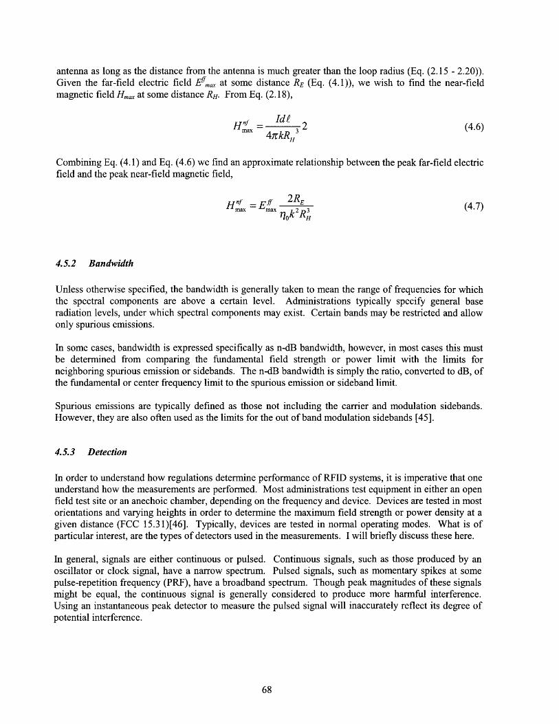
antenna as long as the distance from the antenna is much greater than the loop radius (Eq. (2.15 - 2.20)).Given the far-field electric field Effmx at some distance RE (Eq. (4.1)), we wish to find the near-fieldmagnetic field Hmax, at some distance RH. From Eq. (2.18),
IdHnfx = 2 (4.6)
41rkRH3
Combining Eq. (4.1) and Eq. (4.6) we find an approximate relationship between the peak far-field electricfield and the peak near-field magnetic field,
Hnfx = Ef 2RE (4.7)max max 2 3r70k Rý
4.5.2 Bandwidth
Unless otherwise specified, the bandwidth is generally taken to mean the range of frequencies for whichthe spectral components are above a certain level. Administrations typically specify general baseradiation levels, under which spectral components may exist. Certain bands may be restricted and allowonly spurious emissions.
In some cases, bandwidth is expressed specifically as n-dB bandwidth, however, in most cases this mustbe determined from comparing the fundamental field strength or power limit with the limits forneighboring spurious emission or sidebands. The n-dB bandwidth is simply the ratio, converted to dB, ofthe fundamental or center frequency limit to the spurious emission or sideband limit.
Spurious emissions are typically defined as those not including the carrier and modulation sidebands.However, they are also often used as the limits for the out of band modulation sidebands [45].
4.5.3 Detection
In order to understand how regulations determine performance of RFID systems, it is imperative that oneunderstand how the measurements are performed. Most administrations test equipment in either an openfield test site or an anechoic chamber, depending on the frequency and device. Devices are tested in mostorientations and varying heights in order to determine the maximum field strength or power density at agiven distance (FCC 15.31)[46]. Typically, devices are tested in normal operating modes. What is ofparticular interest, are the types of detectors used in the measurements. I will briefly discuss these here.
In general, signals are either continuous or pulsed. Continuous signals, such as those produced by anoscillator or clock signal, have a narrow spectrum. Pulsed signals, such as momentary spikes at somepulse-repetition frequency (PRF), have a broadband spectrum. Though peak magnitudes of these signalsmight be equal, the continuous signal is generally considered to produce more harmful interference.Using an instantaneous peak detector to measure the pulsed signal will inaccurately reflect its degree ofpotential interference.
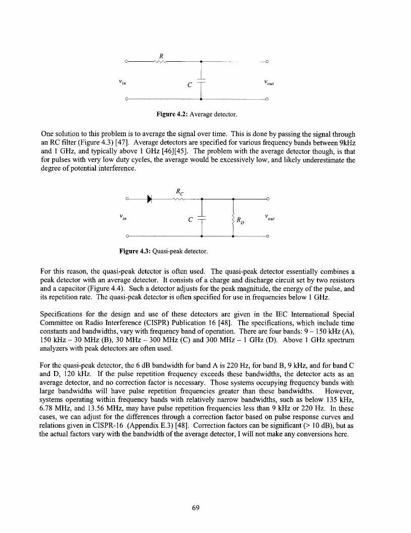
Vin C T ut
Figure 4.2: Average detector.
One solution to this problem is to average the signal over time. This is done by passing the signal throughan RC filter (Figure 4.3) [47]. Average detectors are specified for various frequency bands between 9kHzand 1 GHz, and typically above 1 GHz [46][45]. The problem with the average detector though, is thatfor pulses with very low duty cycles, the average would be excessively low, and likely underestimate thedegree of potential interference.
Re
Figure 4.3: Quasi-peak detector.
For this reason, the quasi-peak detector is often used. The quasi-peak detector essentially combines apeak detector with an average detector. It consists of a charge and discharge circuit set by two resistorsand a capacitor (Figure 4.4). Such a detector adjusts for the peak magnitude, the energy of the pulse, andits repetition rate. The quasi-peak detector is often specified for use in frequencies below 1 GHz.
Specifications for the design and use of these detectors are given in the IEC International SpecialCommittee on Radio Interference (CISPR) Publication 16 [48]. The specifications, which include timeconstants and bandwidths, vary with frequency band of operation. There are four bands: 9 - 150 kHz (A),150 kHz - 30 MHz (B), 30 MHz - 300 MHz (C) and 300 MHz - 1 GHz (D). Above 1 GHz spectrumanalyzers with peak detectors are often used.
For the quasi-peak detector, the 6 dB bandwidth for band A is 220 Hz, for band B, 9 kHz, and for band Cand D, 120 kHz. If the pulse repetition frequency exceeds these bandwidths, the detector acts as anaverage detector, and no correction factor is necessary. Those systems occupying frequency bands withlarge bandwidths will have pulse repetition frequencies greater than these bandwidths. However,systems operating within frequency bands with relatively narrow bandwidths, such as below 135 kHz,6.78 MHz, and 13.56 MHz, may have pulse repetition frequencies less than 9 kHz or 220 Hz. In thesecases, we can adjust for the differences through a correction factor based on pulse response curves andrelations given in CISPR-16 (Appendix E.3) [48]. Correction factors can be significant (> 10 dB), but asthe actual factors vary with the bandwidth of the average detector, I will not make any conversions here.
v12
4.6 Frequencies and Limits
Because RFID systems operating at the lower frequencies rely on manipulation of the near-field electricor magnetic field, I will consider these fields as opposed to the far-field radiated power. When analyzingfar-field systems on the other hand, I will consider the far-field radiated power.
In Table 4.1, the near-field limit and the half-wavelength (resonant antenna) dimension are given for eachfrequency. We can see a suitable grouping for near-field and far-field systems. Those systems from 125kHz to 40.6 MHz should be considered near-field systems, as the near-field limit is suitably large, whilethe half-wavelength dimension is unsuitably large. The systems operating from 483 MHz through 24GHz should operate in the far-field, as the half-wavelength dimension drops to suitable size, while thenear-field becomes unsuitably small.
The various regulatory agencies typically specify general limits for spurious emissions and other limitsfor specific frequency bands. I will describe both the limits for the specific frequency bands of interestand the general limits in the vicinity of these bands.
One should note that in certain configurations, such as tunnel systems, fields may be shielded and thushigher radiation levels than regulations allow may be "seen" inside. When considering RFID systems, wewill consider only unshielded systems.
Regulations that will frequently be referred to include European standards ETSI EN300330 (Inductiveloops from 9 kHz to 25 MHz) [45], EN 300220 (SRDs from 25 MHz to 1000 MHz) [49], EN300440(SRDs from 1 GHz to 40 GHz) [50], and CEPT Rec. 70-03 (SRDs at all radio frequencies) [44], theUnited States regulations, FCC Part 15 [46], and Japan's MPT's Radio Law.
4.6.1 Near-field Operation Frequencies
Each administration defines the field limits for these frequencies differently. The FCC specifies theelectric field at some distance in the far-field. ETSI/CEPT specifies the magnetic field at 10 m which lieseither in the near-field or the far-field depending on the frequency. The MPT specifies the electric field at3 m down to approximately 16 MHz, where the electric field is then specified at the near to far-fieldtransition point for a given frequency. This will be discussed further in the following section.
4.6.1.1 9 kHz - 135 kHz
Though not an ISM band, frequencies in this band are commonly used for short-range radio-communication applications and ISM devices. In addition, several long range services including radio-navigation, time signal, and military radio services use this band [ITU-R SM 1056/ RR]. Field strengthlimits here are generally higher than those at other bands.
CEPT has divided this band into five smaller bands, largely to protect the other radio-communicationservices from harmful interference. They are allocated for inductive applications (70-03 Annex 9). Thesebands and their associated power levels are given in Table 4.2 [44][45].
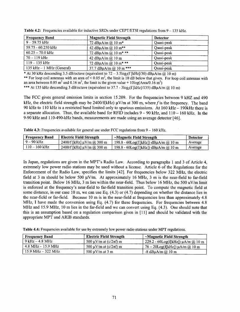
Table 4.2: Frequencies available for inductive SRDs under CEPT/ETSI regulations from 9 - 135 kHz.
Frequency Band Magnetic Field Strength Detector9 - 59.75 kHz 72 dBgA/m @ 10 m* Quasi-peak59.75 - 60.250 kHz 42 dBpA/m @ 10 m** Quasi-peak60.25 - 70.0 kHz 72 dBgA/m @ 10 m* ** Quasi-peak70 - 119 kHz 42 dBgA/m @ 10 m Quasi-peak119 - 135 kHz 72 dBgA/m @ 10 m* ** Quasi-peak135 kHz - 1 MHz (General) 37.7 dBgiA/m @ 10 m *** Quasi-peak
* At 30 kHz descending 3.5 dB/octave (equivalent to 72 - 3.51og 2(f [kHz]/30) dBgA/m @ 10 m)** For loop coil antennas with an area of < 0.05 m2, the limit is 10 dB below that given. For loop coil antennas withan area between 0.05 m2 and 0.16 m2, the limit is the given value + 10log(Area/0.16 m2)
*** At 135 kHz descending 3 dB/octave (equivalent to 37.7 - 31og 2(f [kHz]/135) dBgA/m @ 10 m)
The FCC gives general emission limits in section 15.209. For the frequencies between 9 kHZ and 490kHz, the electric field strength may be 2400/f(kHz) gV/m at 300 m, where fis the frequency. The band90 kHz to 110 kHz is a restricted band limited only to spurious emissions. At 160 kHz - 190kHz there isa separate allocation. Thus, the available band for RFID includes 9 - 90 kHz, and 110 - 160 kHz. In the9-90 kHz and 110-490-kHz bands, measurements are made using an average detector [46].
Table 4.3: Frequencies available for general use under FCC regulations from 9 - 160 kHz.
Frequency Band Electric Field Strength -Magnetic Field Strength Detector9 - 90 kHz 2400/f [kHz] gV/m @ 300 m 198.8 - 60Log(f[kHz]) dBgA/m @ 10 m Average110 - 160 kHz 2400/f [kHz] gV/m @ 300 m 198.8 - 60Log(f[kHz]) dBgA/m @ 10 m Average
In Japan, regulations are given in the MPT's Radio Law. According to paragraphs 1 and 3 of Article 4,extremely low power radio stations may be used without a license. Article 6 of the Regulations for theEnforcement of the Radio Law, specifies the limits [42]. For frequencies below 322 MHz, the electricfield at 3 m should be below 500 gV/m. At approximately 16 MHz, 3 m is the near-field to far-fieldtransition point. Below 16 MHz, 3 m lies within the near-field. Thus below 16 MHz, the 500 uV/m limitis enforced at the frequency's near-field to far-field transition point. To compute the magnetic field atsome distance, in our case 10 m, we can use Eq. (4.3) or (4.7) depending on whether the distance lies inthe near-field or far-field. Because 10 m is in the near-field at frequencies less than approximately 4.8MHz, I have made the conversion using Eq. (4.7) for these frequencies. For frequencies between 4.8MHz and 15.9 MHz, 10 m lies in the far-field and we can convert using Eq. (4.3). One should note thatthis is an assumption based on a regulation comparison given in [ 11] and should be validated with theappropriate MPT and ARIB standards.
Table 4.4: Frequencies available for use by extremely low power radio stations under MPT regulations.
Frequency Band Electric Field Strength -Magnetic Field Strength9 kHz - 4.8 MHz 500 [V/m at (c/2nf) m 229.2 - 60Log(f[kHz]) gA/m @ 10 m4.8 MHz - 15.9 MHz 500 gV/m at (c/2rf) m 76 - 20Log(fjkHz]) gA/m @ 10 m15.9 MHz - 322 MHz 500 gV/m at 3 m -8 dBgA/m @ 10 m
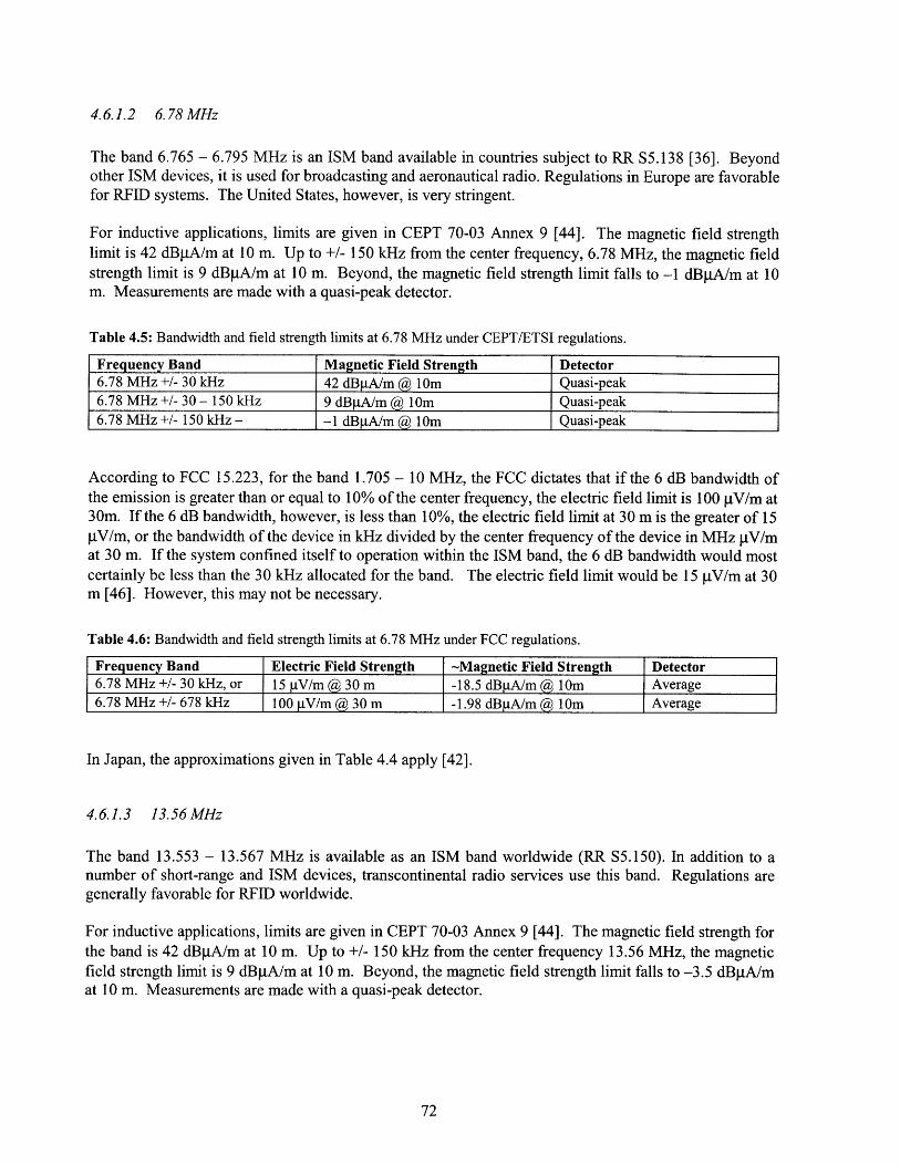
4.6.1.2 6.78 MHz
The band 6.765 - 6.795 MHz is an ISM band available in countries subject to RR S5.138 [36]. Beyondother ISM devices, it is used for broadcasting and aeronautical radio. Regulations in Europe are favorablefor RFID systems. The United States, however, is very stringent.
For inductive applications, limits are given in CEPT 70-03 Annex 9 [44]. The magnetic field strengthlimit is 42 dBgA/m at 10 m. Up to +/- 150 kHz from the center frequency, 6.78 MHz, the magnetic fieldstrength limit is 9 dBgA/m at 10 m. Beyond, the magnetic field strength limit falls to -1 dBgA/m at 10m. Measurements are made with a quasi-peak detector.
Table 4.5: Bandwidth and field strength limits at 6.78 MHz under CEPT/ETSI regulations.
Frequency Band Magnetic Field Strength Detector6.78 MHz +/- 30 kHz 42 dBgA/m @ 10m Quasi-peak6.78 MHz +/- 30 - 150 kHz 9 dBgA/m @ 10m Quasi-peak6.78 MHz +/- 150 kHz - -1 dBgA/m @ 10m Quasi-peak
According to FCC 15.223, for the band 1.705 - 10 MHz, the FCC dictates that if the 6 dB bandwidth ofthe emission is greater than or equal to 10% of the center frequency, the electric field limit is 100 gV/m at30m. If the 6 dB bandwidth, however, is less than 10%, the electric field limit at 30 m is the greater of 15gV/m, or the bandwidth of the device in kHz divided by the center frequency of the device in MHz gV/mat 30 m. If the system confined itself to operation within the ISM band, the 6 dB bandwidth would mostcertainly be less than the 30 kHz allocated for the band. The electric field limit would be 15 gV/m at 30m [46]. However, this may not be necessary.
Table 4.6: Bandwidth and field strength limits at 6.78 MHz under FCC regulations.
Frequency Band Electric Field Strength -Magnetic Field Strength Detector6.78 MHz +/- 30 kHz, or 15 gV/m @ 30 m -18.5 dBgA/m @ 10m Average6.78 MHz +/- 678 kHz 100 gV/m @ 30 m -1.98 dBgA/m @ 10m Average
In Japan, the approximations given in Table 4.4 apply [42].
4.6.1.3 13.56 MHz
The band 13.553 - 13.567 MHz is available as an ISM band worldwide (RR S5.150).number of short-range and ISM devices, transcontinental radio services use this band.generally favorable for RFID worldwide.
In addition to aRegulations are
For inductive applications, limits are given in CEPT 70-03 Annex 9 [44]. The magnetic field strength forthe band is 42 dBWA/m at 10 m. Up to +/- 150 kHz from the center frequency 13.56 MHz, the magneticfield strength limit is 9 dBgA/m at 10 m. Beyond, the magnetic field strength limit falls to -3.5 dBgA/mat 10 m. Measurements are made with a quasi-peak detector.
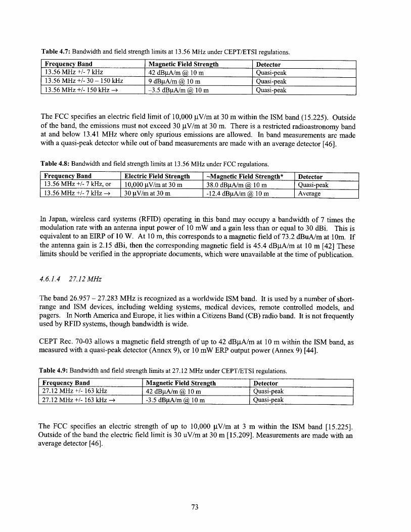
Table 4.7: Bandwidth and field strength limits at 13.56 MHz under CEPT/ETSI regulations.
Frequency Band13.56 MHz +/- 7 kHz13.56 MHz +/- 30 - 150 kHz13.56 MHz +/- 150 kHz --
Magnetic Field Strength42 dBgA/m @ 10 m9 dBgA/m @ 10 mi-3.5 dBCtA/m @ 10 m
The FCC specifies an electric field limit of 10,000 gV/m at 30 m within the ISM band (15.225). Outsideof the band, the emissions must not exceed 30 gV/m at 30 m. There is a restricted radioastronomy bandat and below 13.41 MHz where only spurious emissions are allowed. In band measurements are madewith a quasi-peak detector while out of band measurements are made with an average detector [46].
Table 4.8: Bandwidth and field strength limits at 13.56 MHz under FCC regulations.
Frequency Band Electric Field Strength -Magnetic Field Strength* Detector13.56 MHz +/- 7 kHz, or 10,000 gV/m at 30 m 38.0 dBgA/m @ 10 m Quasi-peak13.56 MHz +/- 7 kHz -> 30 gV/m at 30 m -12.4 dBgA/m @ 10 m Average
In Japan, wireless card systems (RFID) operating in this band may occupy a bandwidth of 7 times themodulation rate with an antenna input power of 10 mW and a gain less than or equal to 30 dBi. This isequivalent to an EIRP of 10 W. At 10 m, this corresponds to a magnetic field of 73.2 dBuA/m at 10m. Ifthe antenna gain is 2.15 dBi, then the corresponding magnetic field is 45.4 dBRtA/m at 10 m [42] Theselimits should be verified in the appropriate documents, which were unavailable at the time of publication.
4.6.1.4 2 7.12 MHz
The band 26.957 - 27.283 MHz is recognized as a worldwide ISM band. It is used by a number of short-range and ISM devices, including welding systems, medical devices, remote controlled models, andpagers. In North America and Europe, it lies within a Citizens Band (CB) radio band. It is not frequentlyused by RFID systems, though bandwidth is wide.
CEPT Rec. 70-03 allows a magnetic field strength of up to 42 dBgA/m at 10 m within the ISM band, asmeasured with a quasi-peak detector (Annex 9), or 10 mW ERP output power (Annex 9) [44].
Table 4.9: Bandwidth and field strength limits at 27.12 MHz under CEPT/ETSI regulations.
Frequency Band Magnetic Field Strength Detector27.12 MHz +/- 163 kHz 42 dBgA/m @ 10 m Quasi-peak27.12 MHz +/- 163 kHz -- -3.5 dB.A/m @ 10 m Quasi-peak
The FCC specifies an electric strength of up to 10,000 ptV/m at 3 m within the ISM band [15.225].Outside of the band the electric field limit is 30 uV/m at 30 m [15.209]. Measurements are made with anaverage detector [46].
DetectorQuasi-peakQuasi-peakQuasi-peak
I
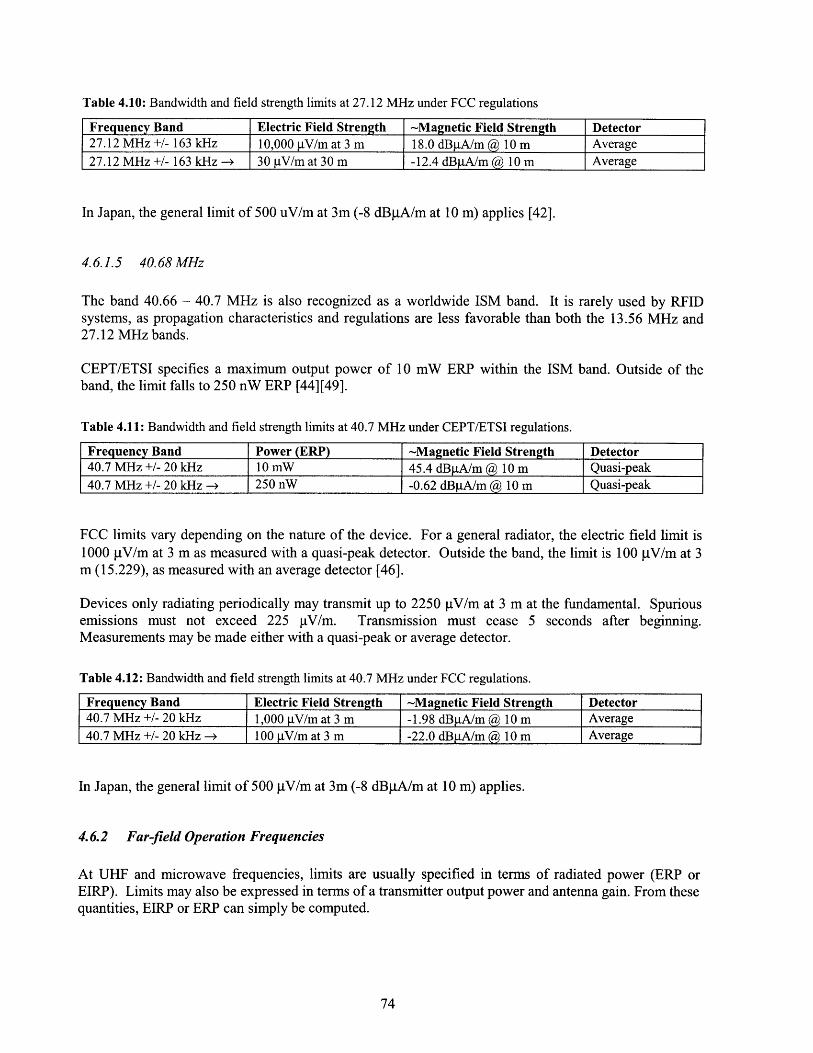
Table 4.10: Bandwidth and field strength limits at 27.12 MHz under FCC regulations
Frequency Band Electric Field Strength -Magnetic Field Strength Detector27.12 MHz +/- 163 kHz 10,000 gV/m at 3 m 18.0 dBgA/m @ 10 m Average27.12 MHz +/- 163 kHz -- 30 gV/m at 30 m -12.4 dBgA/m @ 10 m Average
In Japan, the general limit of 500 uV/m at 3m (-8 dBgA/m at 10 m) applies [42].
4.6.1.5 40.68 MHz
The band 40.66 - 40.7 MHz is also recognized as a worldwide ISM band. It is rarely used by RFIDsystems, as propagation characteristics and regulations are less favorable than both the 13.56 MHz and27.12 MHz bands.
CEPT/ETSI specifies a maximum output power of 10 mW ERP within the ISM band. Outside of theband, the limit falls to 250 nW ERP [44][49].
Table 4.11: Bandwidth and field strength limits at 40.7 MHz under CEPT/ETSI regulations.
Frequency Band Power (ERP) ~Magnetic Field Strength Detector40.7 MHz +/- 20 kHz 10 mW 45.4 dBgA/m @ 10 m Quasi-peak40.7 MHz +/- 20 kHz -4 250 nW -0.62 dBpA/m @ 10 m Quasi-peak
FCC limits vary depending on the nature of the device. For a general radiator, the electric field limit is1000 gV/m at 3 m as measured with a quasi-peak detector. Outside the band, the limit is 100 ptV/m at 3m (15.229), as measured with an average detector [46].
Devices only radiating periodically may transmit up to 2250 gtV/m at 3 m at the fundamental. Spuriousemissions must not exceed 225 gtV/m. Transmission must cease 5 seconds after beginning.Measurements may be made either with a quasi-peak or average detector.
Table 4.12: Bandwidth and field strength limits at 40.7 MHz under FCC regulations.
Frequency Band Electric Field Strength -Magnetic Field Strength Detector40.7 MHz +/- 20 kHz 1,000 gtV/m at 3 m -1.98 dBgA/m @ 10 m Average40.7 MHz +/- 20 kHz - 100 gV/m at 3 m -22.0 dBgA/m @ 10 m Average
In Japan, the general limit of 500 CgV/m at 3m (-8 dBgA/m at 10 m) applies.
4.6.2 Far-field Operation Frequencies
At UHF and microwave frequencies, limits are usually specified in terms of radiated power (ERP orEIRP). Limits may also be expressed in terms of a transmitter output power and antenna gain. From thesequantities, EIRP or ERP can simply be computed.
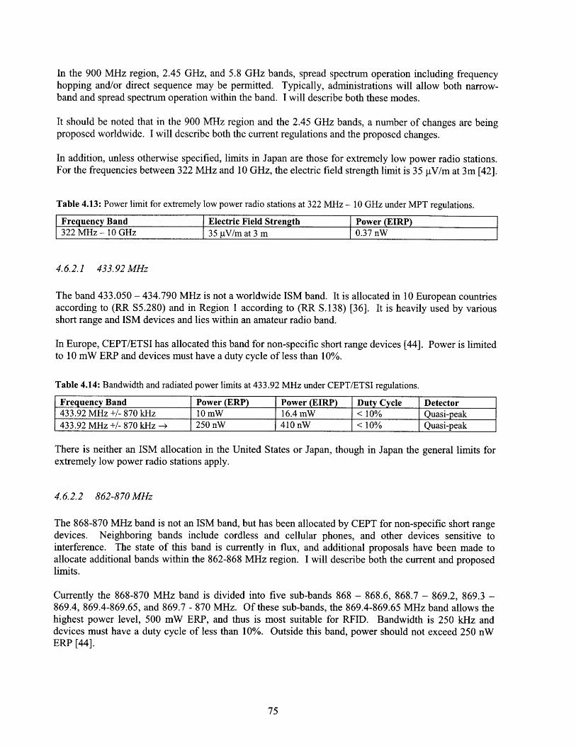
In the 900 MHz region, 2.45 GHz, and 5.8 GHz bands, spread spectrum operation including frequencyhopping and/or direct sequence may be permitted. Typically, administrations will allow both narrow-band and spread spectrum operation within the band. I will describe both these modes.
It should be noted that in the 900 MHz region and the 2.45 GHz bands, a number of changes are beingproposed worldwide. I will describe both the current regulations and the proposed changes.
In addition, unless otherwise specified, limits in Japan are those for extremely low power radio stations.For the frequencies between 322 MHz and 10 GHz, the electric field strength limit is 35 pV/m at 3m [42].
Table 4.13: Power limit for extremely low power radio stations at 322 MHz - 10 GHz under MPT regulations.
Frequency Band Electric Field Strength Power (EIRP)322 MHz - 10 GHz 35 gV/m at 3 m 0.37 nW
4.6.2.1 433.92 MHz
The band 433.050 - 434.790 MHz is not a worldwide ISM band. It is allocated in 10 European countriesaccording to (RR S5.280) and in Region 1 according to (RR S.138) [36]. It is heavily used by variousshort range and ISM devices and lies within an amateur radio band.
In Europe, CEPT/ETSI has allocated this band for non-specific short range devices [44]. Power is limitedto 10 mW ERP and devices must have a duty cycle of less than 10%.
Table 4.14: Bandwidth and radiated power limits at 433.92 MHz under CEPT/ETSI regulations.
Frequency Band Power (ERP) Power (EIRP) Duty Cycle Detector433.92 MHz +/- 870 kHz 10 mW 16.4 mW < 10% Quasi-peak433.92 MHz +/- 870 kHz - 250 nW 410 nW < 10% Quasi-peak
There is neither an ISM allocation in the United States or Japan, though in Japan the general limits forextremely low power radio stations apply.
4.6.2.2 862-870 MHz
The 868-870 MHz band is not an ISM band, but has been allocated by CEPT for non-specific short rangedevices. Neighboring bands include cordless and cellular phones, and other devices sensitive tointerference. The state of this band is currently in flux, and additional proposals have been made toallocate additional bands within the 862-868 MHz region. I will describe both the current and proposedlimits.
Currently the 868-870 MHz band is divided into five sub-bands 868 - 868.6, 868.7 - 869.2, 869.3 -869.4, 869.4-869.65, and 869.7 - 870 MHz. Of these sub-bands, the 869.4-869.65 MHz band allows thehighest power level, 500 mW ERP, and thus is most suitable for RFID. Bandwidth is 250 kHz anddevices must have a duty cycle of less than 10%. Outside this band, power should not exceed 250 nWERP [44].
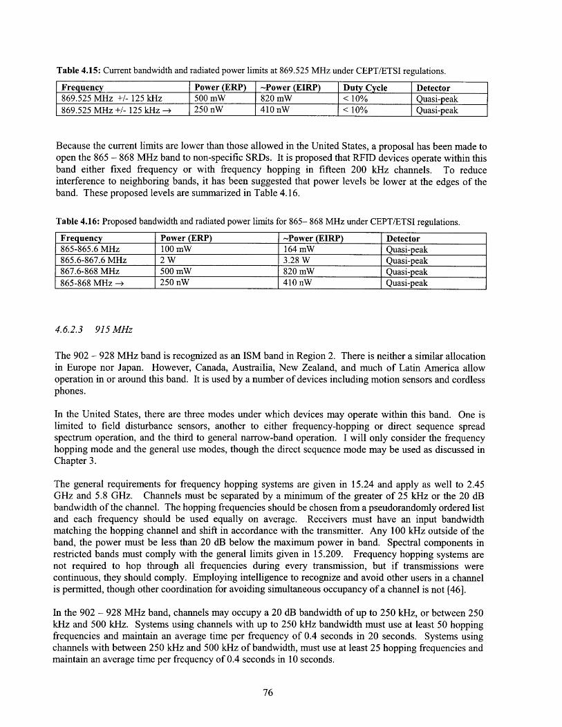
Table 4.15: Current bandwidth and radiated power limits at 869.525 MHz under CEPT/ETSI regulations.
Frequency Power (ERP) -Power (EIRP) Duty Cycle Detector869.525 MHz +/- 125 kHz 500 mW 820 mW < 10% Quasi-peak869.525 MHz +/- 125 kHz - 250 nW 410 nW < 10% Quasi-peak
Because the current limits are lower than those allowed in the United States, a proposal has been made toopen the 865 - 868 MHz band to non-specific SRDs. It is proposed that RFID devices operate within thisband either fixed frequency or with frequency hopping in fifteen 200 kHz channels. To reduceinterference to neighboring bands, it has been suggested that power levels be lower at the edges of theband. These proposed levels are summarized in Table 4.16.
Table 4.16: Proposed bandwidth and radiated power limits for 865- 868 MHz under CEPT/ETSI regulations.
Frequency Power (ERP) -Power (EIRP) Detector865-865.6 MHz 100 mW 164 mW Quasi-peak865.6-867.6 MHz 2 W 3.28 W Quasi-peak867.6-868 MHz 500 mW 820 mW Quasi-peak865-868 MHz - 250 nW 410 nW Quasi-peak
4.6.2.3 915 MHz
The 902 - 928 MHz band is recognized as an ISM band in Region 2. There is neither a similar allocationin Europe nor Japan. However, Canada, Austrailia, New Zealand, and much of Latin America allowoperation in or around this band. It is used by a number of devices including motion sensors and cordlessphones.
In the United States, there are three modes under which devices may operate within this band. One islimited to field disturbance sensors, another to either frequency-hopping or direct sequence spreadspectrum operation, and the third to general narrow-band operation. I will only consider the frequencyhopping mode and the general use modes, though the direct sequence mode may be used as discussed inChapter 3.
The general requirements for frequency hopping systems are given in 15.24 and apply as well to 2.45GHz and 5.8 GHz. Channels must be separated by a minimum of the greater of 25 kHz or the 20 dBbandwidth of the channel. The hopping frequencies should be chosen from a pseudorandomly ordered listand each frequency should be used equally on average. Receivers must have an input bandwidthmatching the hopping channel and shift in accordance with the transmitter. Any 100 kHz outside of theband, the power must be less than 20 dB below the maximum power in band. Spectral components inrestricted bands must comply with the general limits given in 15.209. Frequency hopping systems arenot required to hop through all frequencies during every transmission, but if transmissions werecontinuous, they should comply. Employing intelligence to recognize and avoid other users in a channelis permitted, though other coordination for avoiding simultaneous occupancy of a channel is not [46].
In the 902 - 928 MHz band, channels may occupy a 20 dB bandwidth of up to 250 kHz, or between 250kHz and 500 kHz. Systems using channels with up to 250 kHz bandwidth must use at least 50 hoppingfrequencies and maintain an average time per frequency of 0.4 seconds in 20 seconds. Systems usingchannels with between 250 kHz and 500 kHz of bandwidth, must use at least 25 hopping frequencies andmaintain an average time per frequency of 0.4 seconds in 10 seconds.
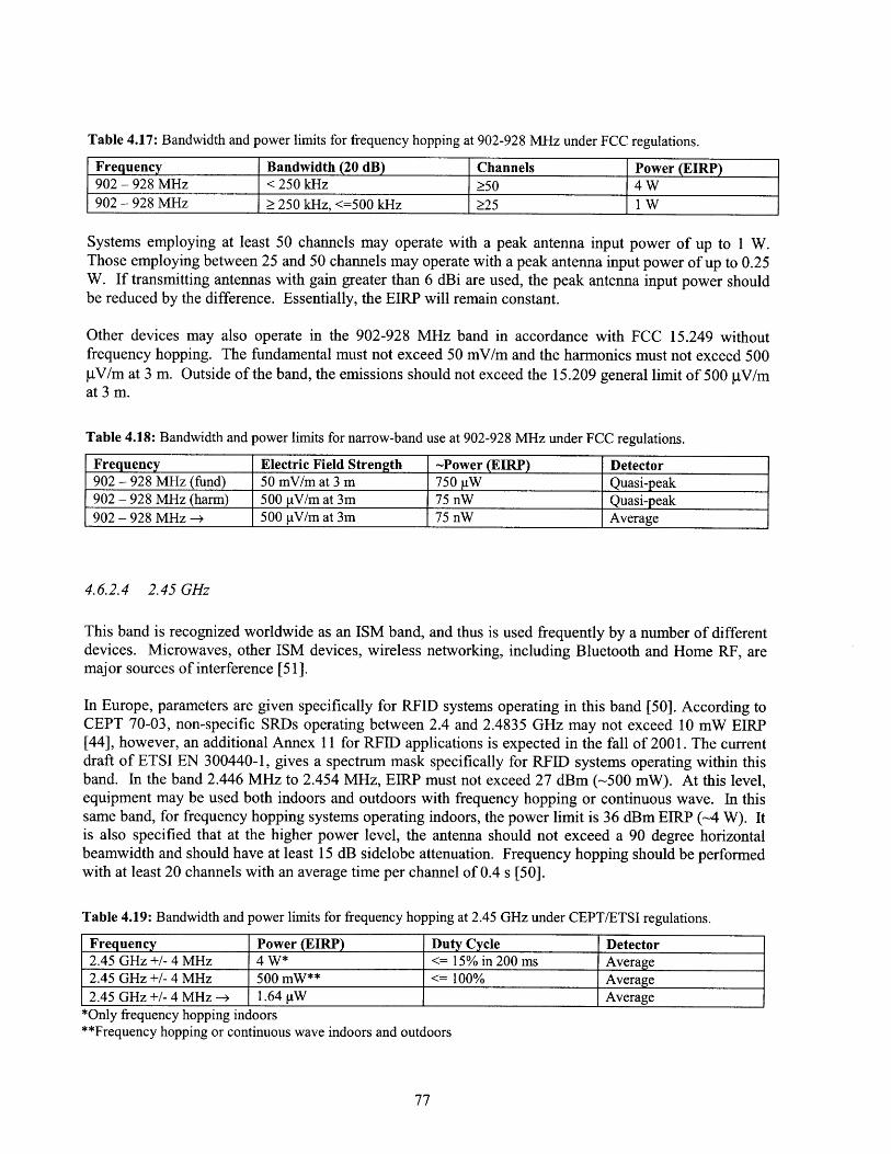
Table 4.17: Bandwidth and power limits for frequency hopping at 902-928 MHz under FCC regulations.
Frequency Bandwidth (20 dB) Channels Power (EIRP)902 - 928 MHz < 250 kHz >50 4 W902 - 928 MHz > 250 kHz, <=500 kHz >25 1 W
Systems employing at least 50 channels may operate with a peak antenna input power of up to 1 W.Those employing between 25 and 50 channels may operate with a peak antenna input power of up to 0.25W. If transmitting antennas with gain greater than 6 dBi are used, the peak antenna input power shouldbe reduced by the difference. Essentially, the EIRP will remain constant.
Other devices may also operate in the 902-928 MHz band in accordance with FCC 15.249 withoutfrequency hopping. The fundamental must not exceed 50 mV/m and the harmonics must not exceed 500gV/m at 3 m. Outside of the band, the emissions should not exceed the 15.209 general limit of 500 gV/mat 3 m.
Table 4.18: Bandwidth and power limits for narrow-band use at 902-928 MHz under FCC regulations.
Frequency Electric Field Strength -Power (EIRP) Detector902 - 928 MHz (fund) 50 mV/m at 3 m 750 pW Quasi-peak902 - 928 MHz (harm) 500 pV/m at 3m 75 nW Quasi-peak902 - 928 MHz -4 500 pV/m at 3m 75 nW Average
4.6.2.4 2.45 GHz
This band is recognized worldwide as an ISM band, and thus is used frequently by a number of differentdevices. Microwaves, other ISM devices, wireless networking, including Bluetooth and Home RF, aremajor sources of interference [51].
In Europe, parameters are given specifically for RFID systems operating in this band [50]. According toCEPT 70-03, non-specific SRDs operating between 2.4 and 2.4835 GHz may not exceed 10 mW EIRP[44], however, an additional Annex 11 for RFID applications is expected in the fall of 2001. The currentdraft of ETSI EN 300440-1, gives a spectrum mask specifically for RFID systems operating within thisband. In the band 2.446 MHz to 2.454 MHz, EIRP must not exceed 27 dBm (-500 mW). At this level,equipment may be used both indoors and outdoors with frequency hopping or continuous wave. In thissame band, for frequency hopping systems operating indoors, the power limit is 36 dBm EIRP (-4 W). Itis also specified that at the higher power level, the antenna should not exceed a 90 degree horizontalbeamwidth and should have at least 15 dB sidelobe attenuation. Frequency hopping should be performedwith at least 20 channels with an average time per channel of 0.4 s [50].
Table 4.19: Bandwidth and power limits for frequency hopping at 2.45 GHz under CEPT/ETSI regulations.
Frequency Power (EIRP) Duty Cycle Detector2.45 GHz +/- 4 MHz 4 W* <= 15% in 200 ms Average2.45 GHz +/- 4 MHz 500 mW** <= 100% Average2.45 GHz +/- 4 MHz -- 1.64 tiW Average
*Only frequency hopping indoors**Frequency hopping or continuous wave indoors and outdoors
I
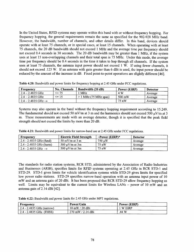
In the United States, RFID systems may operate within this band with or without frequency hopping. Forfrequency hopping, the general requirements remain the same as specified for the 902-928 MHz band.However, the bandwidth, number of channels, and other details differ. In this band, devices shouldoperate with at least 75 channels, or in special cases, at least 15 channels. When operating with at least75 channels, the 20 dB bandwidth should not exceed 1 MHz and the average time per frequency shouldnot exceed 0.4 seconds in 30 seconds. The 20 dB bandwidth may be greater than 1 MHz, if the systemuses at least 15 non-overlapping channels and their total span is 75 MHz. Under this mode, the averagetime per frequency should be 0.4 seconds in the time it takes to hop through all channels. If the systemuses at least 75 channels, the antenna input power should not exceed 1 W. If using fewer channels, itshould not exceed .125 W. If an antenna with gain greater than 6 dBi is used, the input power should bereduced by the amount of the increase in dB. Fixed point-to-point operations are slightly different [46].
Table 4.20: Bandwidth and power limits for frequency hopping at 2.45 GHz under FCC regulations.
Frequency No. Channels Bandwidth (20 dB) Power (EIRP) Detector2.4 - 2.4835 GHz <= 75 1 MHz 4 W Average2.4 - 2.4835 GHz <= 15 > 1 MHz (75 MHz span) 500 mW Average2.4 - 2.4835 GHz -4 75 nW Average
Systems may also operate in the band without the frequency hopping requirement according to 15.249.The fundamental should not exceed 50 mV/m at 3 m and the harmonics should not exceed 500 PV/m at 3m. These measurements are made with an average detector, though it is specified that the peak fieldstrength should not exceed the limits by more than 20 dB.
Table 4.21: Bandwidth and power limits for narrow-band use at 2.45 GHz under FCC regulations.
Frequency Electric Field Strength -Power (EIRP)* Detector2.4 - 2.4835 GHz (fund) 50 mV/m at 3 m 750 [tW Average2.4 - 2.4835 GHz (harm) 500 jV/m at 3m 75 nW Average2.4 - 2.4835 GHz -- 500 jiV/m at 3m 75 nW Average
The standards for radio station systems, RCR STD, administered by the Association of Radio Industriesand Businesses (ARIB), specifies limits for RFID systems operating at 2.45 GHz in RCR STD-1 andSTD-29. STD-1 gives limits for vehicle identification systems while STD-29 gives limits for specifiedlow power radio stations. STD-29 specifies narrow-band operation with an antenna input power of 10mW and an antenna gain of 20 dBi. It has been proposed that RCR STD-29 allow frequency hopping aswell. Limits may be equivalent to the current limits for Wireless LANs - power of 10 mW and anantenna gain of 2.14 dBi [42].
Table 4.22: Bandwidth and power limits for 2.45 GHz under MPT regulations.
Frequency Power/Gain Power (EIRP)2.4 - 2.4835 GHz (narrow) 10 mW / 20 dBi 1 W EIRP2.4 -2.4835 GHz (FHSS) 270 mW / 2.14 dBi .44 W
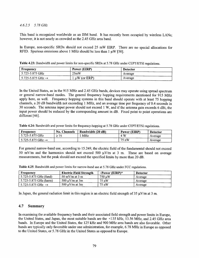
4.6.2.5 5.78 GHz
This band is recognized worldwide as an ISM band. It has recently been occupied by wireless LANs;however, it is not nearly as crowded as the 2.45 GHz area band.
In Europe, non-specific SRDs should not exceed 25 mW EIRP. There are no special allocations forRFID. Spurious emissions above 1 MHz should be less than 1 gW [50].
Table 4.23: Bandwidth and power limits for non-specific SRDs at 5.78 GHz under CEPT/ETSI regulations.
Frequency Power (EIRP) Detector5.725-5.875 GHz 25mW Average5.725-5.875 GHz - 1 jtW (or ERP) Average
In the United States, as in the 915 MHz and 2.45 GHz bands, devices may operate using spread spectrumor general narrow-band modes. The general frequency hopping requirements mentioned for 915 MHzapply here, as well. Frequency hopping systems in this band should operate with at least 75 hoppingchannels, a 20 dB bandwidth not exceeding 1 MHz, and an average time per frequency of 0.4 seconds in30 seconds. The antenna input power should not exceed 1 W, and if the antenna gain exceeds 6 dBi, theinput power should be reduced by the corresponding amount in dB. Fixed point to point operations aredifferent [46].
Table 4.24: Bandwidth and power limits for frequency-hopping at 5.78 GHz under CEPT/ETSI regulations.
Frequency No. Channels Bandwidth (20 dB) Power (EIRP) Detector5.725-5.875 GHz 2 75 1 MHz 4 W Average5.725-5.875 GHz - 75 nW Average
For general narrow-band use, according to 15.249, the electric field of the fundamental should not exceed50 mV/m and the harmonics should not exceed 500 gV/m at 3 m. These are based on averagemeasurements, but the peak should not exceed the specified limits by more than 20 dB.
Table 4.25: Bandwidth and power limits for narrow-band use at 5.78 GHz under FCC regulations.
Frequency Electric Field Strength -Power (EIRP)* Detector5.725-5.875 GHz (fund) 50 mV/m at 3 m 750 1tW Average5.725-5.875 GHz (harm) 500 jV/m at 3m 75 nW Average5.725-5.875 GHz -4 500 jtV/m at 3m 75 nW Average
In Japan, the general radiation limit in this region is an electric field strength of 35 gV/m at 3 m.
4.7 Summary
In examining the available frequency bands and their associated field strength and power limits in Europe,the United States, and Japan, the most suitable bands are the <135 kHz, 13.56 MHz, and 2.45 GHz areabands. In Europe and the United States, the 125 kHz and 900 MHz area bands are also favorable. Otherbands are typically only favorable under one administration, for example, 6.78 MHz in Europe as opposedto the United States, or 5.78 GHz in the United States as opposed to Europe.

In selecting an operating frequency, in addition to available bandwidth, field strength and power levels,and interference, a number of other factors should be considered. These include not only propagation andbehavior in various environments, as discussed in Chapter 2, but also influences on system design andimplementation. We will discuss these factors in Chapter 5.
Chapter 5
PHYSICAL IMPLEMENTATION
5.1 Introduction
In Chapter 2 we have seen how electromagnetic fields and wave behave. In Chapter 3, we have seen thetheory that describes how tags are able to communicate through modulations of the electromagneticfields. In Chapter 4, we have seen how the both electromagnetic fields and their modulations aregoverned by regulations. Now we will study how the tag's basic functions, with their overridingconstraints, are physically implemented.
The physical implementation of tags is extremely important on the basis of cost and performance.Though both factors are important to the adoption and benefit of the technology, it is cost, which is ofprimary importance. Passive tags, just like everyday consumable objects we buy, have a finite life. Theywill be fabricated and destroyed just as often as consumable items. At the huge volumes of tags expectedto be used and produced, minute increases in the cost of a single tag will create massive increases in theoverall cost of their use. A tag's performance is determined not only by the tag, but by the readers andassociated infrastructure. A tag's cost, on the other hand, is determined only by the tag itself- its designand manufacture, and the volume at which it is produced. For this reason, we must understand thephysical components necessary to make a tag function and their influence on cost.
A tag consists of an antenna attached to an electronic circuit. The antenna acts as a transducer betweenelectromagnetic fields and electric energy. A transmission line transfers this energy to circuitry and viceversa. The circuitry processes the energy, stores it, uses it, and redirects it back through the transmissionline and antenna, causing controlled responses.
First I will briefly discuss some of the antennas applicable to RFID tags. I will then discuss the tag'sintegrated circuit, including a review of its various components and overall power consumptioncharacteristics. My focus in this chapter is on cost and performance issues associated directly with thedesign and implementation of the tag. Manufacturing is without doubt, extremely important, and deservesextensive treatment. However, here I will merely touch on some of the more important issues.
5.2 Antennas
As we know there are two main types of RFID tags - those that operate in the near-field and those thatoperate in the far-field. Just as the way they interact with the electromagnetic fields and waves isfundamentally different, so is the design of the antennas they use. I will first describe near-field antennas,followed by far-field antennas.
5.2.1 Near-field
Systems in the near-field are either inductively coupled or capacitively coupled. Inductively coupledsystems interact with the magnetic field, while capacitively coupled systems interact with the electricfield. As we have seen, loop antennas are the desired configuration for inductively coupled systems astheir radiated magnetic field dominates the electric field. For capactively coupled systems, however,other antennas such as dipoles and electrode antennas are preferred. I will focus on inductively coupledsystems and loop antennas.
Several characteristics affect a loop antenna's cost and performance. Loop area and number of turns relatedirectly to the magnetic flux through the antenna, the resulting induced voltage and current, and theachievable range. In addition, a larger area and more turns mean more material and higher cost.Materials, due to variations in impedance and quality factor, also affect range. Due to variations in theircost and manufacture, materials also affect cost. I will briefly examine the affects of loop size andmaterials on the basis of performance and cost.
If we examine Eq. (2.29), we see the direct relationship between induced voltage, area enclosed by theloop, number of turns, and frequency.
v,2 = jwN 2 1uH,A2 cosV
Other factors include orientation, which we can assume to be maximized, and permeability, which is aconstant for free space. Permeability may be increased through the incorporation of ferrites as a core, yetthis will increase directivity.
The relationship between frequency, number of turns, and area is of particular importance. For maximuminduced voltage, the tag's loop should typically be matched to the area of the reader loop. However, dueto application size constraints and material cost, the size of the tag's loop is usually limited. We also notethat tags operating at lower frequencies, 125 kHz for example, need almost 110 times the number of turnsused at 13.56 MHz, for similar performance.
The number of turns of the loop antenna also affects the inductance and the resistive losses of the loop. Asan example, we can consider a circular loop (rectangular loops are also common). The inductance for acircular loop is given by Eq. (2.31)
L2 = PbN2 [In( 8b 1.75
We also note that inductance increases with the coil radius, or area. Resistance for a circular loop is givenby Eq. (2.33)
R g = N2 b mya 2c
where a is the material conductivity.
How the extra area and the number of turns affect cost, is determined largely by the material used.

Loop antennas are typically made either by wound wire or printed conductive ink. Both of these methodshave a direct affect on both performance and cost. Inherent in the material used in a loop antenna is aninductance and a resistance. For a maximized quality factor, resistive losses should be minimized, whileinductivity should be maximized. Though it may not always be desirable for a maximum quality factordue to detuning effects when surrounded by other antennas and conductors, it will provide maximumvoltage.
When large numbers of turns are required, copper wire is generally used. Because resistive losses in wireincrease with decreasing diameters, Q decreases. Resistivity of a copper wire is approximately 0.017Omm 2/m.
Printed conducting ink and paste may be used as well, though their use is typically limited to loops withlow numbers of turns. Various inks may be used, though silver is used most frequently for its highconductivity relative to cost. Similar to copper wire, printed antenna losses increase with decreasing linewidths. Resistivities for silver conductive paste typically vary between 0.01 and 0.05 a/square for athickness of 1 mil. Resistivities for carbon-based conductive paste typically vary between 10 and 50Q/square for a thickness of 1 mil [52]. Actual resistivity is sensitive to curing temperature and rate, andother factors.
Another concern is the size of the tuning capacitor necessary to create the appropriate resonance. Atlower frequencies where numbers of coils are larger, inductance will likely be higher as well. As such,capacitances will also need to be larger. We will see that capacitors can consume relatively large areas onan integrated circuit, and thus radically increase cost.
One must also consider the impedance used for the load modulation. It may be a capacitor or resistor, ora combination of the two. To decrease power consumption and component size, this impedance should beminimized while ensuring that the signal is still detectable by the reader.
5.2.2 Far-field
Systems in the far-field interact directly with electromagnetic waves. As we have seen, radiation andreception characteristics improve drastically for antennas with at least one dimension on the order of halfof a wavelength. At this size antennas are resonant and have a real input impedance. This makes forimproved radiation and reception efficiency, easier matching, and more power delivered to and from theattached circuitry.
We should note that systems operating in the far-field do not necessarily have to incorporate half-wavelength dimensioned antennas. Smaller dimensioned antennas may be used, however, input reactancewill increase and input resistance will decrease. This may create difficulties in matching, and will resultin lower radiation efficiency, meaning less power available to the tag, and less power available to bescattered back to the reader. It certain cases, though, this may be beneficial, as the structural mode scatterthat contributes directly to noise, will be reduced.
There are several types of resonant antennas. Commonly used types include half-wave and foldeddipoles, and various shapes of microstrip patch antennas. Generally, dipole antennas may use wires, orthey may be printed onto a substrate. Microstrip patch antennas are printed onto a dielectric, often aprinted circuit board material, with a conducting ground plane underneath. I will briefly discuss some ofthe performance and cost related issues of these antennas.
5.2.2.1 Dipole Antennas
Wire dipoles can be more costly than printed dipoles due to manufacturing processes, so for very low costapplications, printed dipoles may be preferred. It is important to reduce ohmic losses in the antenna, sogenerally, the dipole width should be relatively wide. The material used should also have a low resistivityand a high quality factor.
Though they provide more efficient power transfer, half-wave dipoles, by virtue of their resonance, canhave a relatively narrow bandwidth. Bandwidth can be increased, though, by increasing the widths, oreffective diameters [13].
5.2.2.2 Microstrip Patch Antennas
Microstrip patch antennas are planar antennas that are typically printed directly onto a dielectric circuitboard. They consist of three layers: the conductive patch on top, a conductive ground plane on thebottom, and a dielectric material in between. The patch is usually some appreciable fraction of awavelength in dimensions, while the ground plane extends further in dimensions. The dielectric materialis typically some printed circuit board material - often, PTFE, or Alumina. Because they have a groundplane, their radiation pattern is limited to the area above the ground plane [53].
The patch can take any number of shapes. Rectangular, circular, and elliptic patches are commonly used.Different shapes are often explored to vary the various parameters, including input impedance, radiationefficiency, and polarization. Patches are fed through a small transmission line, either directly, coupledelectromagnetically, or through an aperture. Each feed-line method has its own degree of freedoms, butlike the patch shape, the main factors that they influence are input impedance, radiation efficiency, andpolarization.
Bandwidth is an important concern with patch antennas as basic designs typically have a fractionalbandwidth relative to the center frequency of only a few percent. For a rectangular patch, the fractionalbandwidth can be given by [13]
E r-1W tB = 3.77 W (5.1)
Er2 LA
where er is the relative permittivity of the dielectric, W is the patch width, L is the patch length, and t isthe thickness. We see that increasing thickness increases bandwidth, while increasing the dielectricpermittivity decreases bandwidth. Selection of dielectric is important not only for bandwidth but foroverall performance of the patch. Dielectrics should have minimal losses, high temperature stability, highdimensional stability, and uniformity.
Microstrip patch antennas can be costlier than printed dipoles, as they require the ground plane anddielectric material. Printed dipoles of course need a substrate, yet the substrate material does not have asgreat as an affect on performance as does the patch dielectric.
In general, performance offered by dipoles and patch antennas can be comparable, and their use in manyways depends on the application, the operating frequency, and the cost of materials and manufacture.
_ _
5.3 Integrated Circuit
For reasons outlined in the introduction, I have assumed the use of an integrated circuit - moreparticularly, a single integrated circuit. Often it may be desirable to use external discrete components inaddition to a chip. While this may be acceptable for low volume applications, for reasons of cost,manufacturing, and performance, the tag should have only a single integrated circuit.
The goal of this section is not to design an integrated circuit, but rather to describe the variouscomponents necessary for its function, including their effects on performance and cost. The moreimportant variables controlled by the chip include - power consumption, size, and cost. Because the tagrelies on electromagnetic fields for power, energy is limited. Power consumption must be reduced andmanaged in a way so as not to detrimentally affect the performance of the tag, principally its operatingrange. Size directly affects cost. In general, the more silicon used, the more expensive the chip. Thenumber of components used, and their size should be reduced to minimize cost. It should be noted,however, that more efficient use of gates can lead to more switching per gate, which leads directly tohigher power consumption. We will discuss this tradeoff in a later section.
5.3.1 Overall Architecture
Before describing the various components used in integrated circuits, I will briefly discuss the overallarchitecture of RFID tags. Whether they operate in the near-field or far-field, their overall architecture issimilar.
A tag, which is simply a carrier for a unique identification number must perform several basic functions.It must receive and rectify the incoming signal for the extraction of energy and information. It must storeand manage the extracted energy to power the tag. From the extracted information it must establish aclocking signal with which to drive its digital circuitry. Through this circuitry, it must process theinformation and make the appropriate modulations of the incoming signal through load or backscattermodulation as described in Chapters 2 and 3.
The RF front end is responsible for bi-directional interfacing between the antenna and other functionalblocks of the tag. In the RF front end, energy and data are extracted from the input signal and sent topower supply, biasing, clock recovery, and data processing circuitry [54][55]. Because of the largevariations in field strength with respect to distance, over-voltage protection is also located in the front-end. As directed by the data processing circuitry, information is modulated back through the antenna tothe reader.
The power supply, biasing, clock recovery, and data processing circuitry are implemented in acombination of analog and digital circuits. Memory is also included. In the case of read-only tags, it istypically read-only memory (ROM) or write once read many (WORM).
5.3.2 Components
The components necessary to perform the tag's functions include analog and digital circuits with passivecomponents, active components, and memory. They all may be incorporated and interconnected in asingle integrated circuit. Because many of the current fabrication processes were designed for digitalcircuitry, implementation of analog circuits next to digital circuits can be difficult. One problem isreduced yield, as analog circuits tend to suffer more variations [56]. In addition, as we will see, important
passive components can require relatively excessive amounts of area, and given their loose tolerances,still offer only satisfactory performance.
After briefly describing the physics of semiconductors, I will describe the various pertinent components.I will begin with transistors, followed by passive components, diodes, and other important devices,including oscillators, phase-locked loops, digital circuits, and memory. Finally I will describe the overallpower consumption characteristics. I will not describe the fabrication process and interconnect propertiesin any depth.
5.3.2.1 Semiconductors and Transistors
Semiconductor materials are those that are neither good insulators nor good conductors. They are madeby introducing controlled amounts of impurity atoms in a process called doping. By doping a region of amaterial with another material having more valence electrons, the region becomes an "n-type" region.Alternatively doping with a material having fewer valence electrons, the region becomes a "p-type"region. Applying a voltage causes excess electrons to move. Silicon is the most common material usedfor semiconducting devices for various reasons. It is abundant in nature and is relatively insensitive totemperature various due to its large bandgap. Gallium Arsenide is used for its speed advantages - it canbe over twice as fast. Gallium Arsenide, however, is more expensive than standard Silicon, and notnearly as abundant [57][58].
Transistors, which are semiconducting devices, have been in development since the late 1940's. Bipolartechnologies were developed first, followed by metal-oxide semiconductor (MOS) technologies. MOStechnologies offered reduction in size and power consumption. P types (PMOS) were developed first,followed by N types (NMOS). Complimentary MOS (CMOS) devices were developed for furtherreduction in power consumption at a cost of an increase in size. BiCMOS devices combine fast bipolartechnologies with the power efficiency of CMOS. The CMOS market however, dwarfs those of othertechnologies, and for the foreseeable future, it is expected that CMOS will have a significant costadvantage [59].
A MOS device, in some respects, can be thought of as a parallel plate capacitor. A simple example is anNMOS device. The gate, which is typically heavily doped polysilicon, represents one plate, which isseparated from the semiconductor, the other plate, by a dielectric material. The gate lies above andbetween two heavily doped n-type regions - one the source, and the other, the drain. All other regions onthe semiconductor are p-type regions.
When there is no voltage at the gate, there is no conductivity on the device. When voltage is applied atthe gate however, an electric field is created which induces charges of opposite polarity in thesemiconductor. When enough voltage is applied, charges are pulled from the surface of thesemiconductor and electrons from the source and drain create an "inversion" layer. This inversion layer isa conductive path between the source and the drain. Charges moving at a velocity derived from theelectric field and the electron mobility produce a current. Variation of the relative sizes, distances, andvoltages produces a number of different effects.
These devices have both static and dynamic effects. The dynamic effects are dominated by capacitancesat various places in the device. The source and drain form a capacitance from a reverse bias junction withthe substrate. In addition, parallel plate capacitances are formed between the gate and the source, and thegate and the drain, as well as from the gate to the channel and the channel to the bulk material.
Complimentary metal oxide (CMOS) devices combine PMOS devices with NMOS devices. Thoughlarger, they provide reduced power consumption. Transistors can be regarded as the main building blockof an integrated circuit because they may be used as passive components, such as resistors and capacitors,as well as active components.
5.3.2.2 Passive Components
In RFID tags, passive components are particularly important for the RF front end and power managementsystems. I will briefly review their use in integrated circuits.
5.3.2.2.1 Resistors
There are relatively few good options for creating resistors in standard CMOS technology. Interconnectmaterial such as polysilicon, metal, or other more specialized materials, may often be deposited inbending lines. Polysilicon is typically more resistive than metal and offers approximately 5-10 2 persquare with a tolerance of around 35%. It also has a low parasitic capacitance per area, a moderatetemperature coefficient, and a low voltage coefficient. Metal typically gives on the order of 10 M92 persquare [60].
Wells are another option when high resistances are needed. They offer resistivities in the range of 1-10k.Q per square, yet they suffer from large parasitic capacitances due to the junction between the well andthe substrate. They have an initial tolerance of 50-80%, a large temperature coefficient, and a largevoltage coefficient.
A MOS transistor may also be used as a compact resistor. It, however, has a loose tolerance and hightemperature coefficient due to its dependence on electron mobility. N-type or p-type source-draindiffusions are another option, which provide similar resistivity and temperature coefficients topolysilicon. Parasitic capacitance can be significant, and the voltage coefficient is noticeable [60].
5.3.2.2.2 Capacitors
Capacitors can be formed in a number of ways. One common method is through creating parallel platecapacitances with interconnect material. Because the inter-level dielectric is relatively thick, capacitanceper area is typically small (5x10⁻⁵ pF/gm2). Parasitic capacitance from layers directly below, can bedetrimental to performance and may have 10-30% of the main capacitance.
Interconnect material can also be used to create capacitance through lateral lines, along with parallel platemethods. As the capacitance depends on perimeter, some have used fractals for their large perimeter withrespect to area. Such methods may offer factor of 10 increases in capacitance [60].
Because of the gate capacitance common to a transistor, a MOS device may also be used. Depending onthe dielectric thickness, capacitances of 1-5 fF/ m 2 may be achieved.
Another option is to use the junction capacitance inherent in a p to n well junction. Because the junctioncapacitance depends on the applied bias, capacitance can be tuned in this way [60].
5.3.2.2.3 Inductors
Inductors with low noise, distortion, and power consumption are typically hard to implement in CMOStechnology. The planar spiral is the most widely used inductor, yet it suffers from large areas for minorinductances. Losses due to resistance and non-uniform current distribution can be large. In addition,parasitic capacitances are formed with surrounding structures so resonance can be formed limiting theinductor's usefulness. Quality factors are very low compared to those of discrete components [56].
5.3.2.3 Charge Pumps
Charge pumps may be used for situations where a high voltage relative to the available voltage must begenerated. Often charge pumps will be used to supply a high voltage for writing to EEPROM. They arecreated by connecting multiple stages of switched capacitors. When each stage is charged, voltages canbe combined to create a higher output voltage.
5.3.2.4 Diodes
Diodes are necessary in RFID tags for rectification of incoming signals for both energy extraction andsignal detection. They may be made from transistors, yet because transistors may have a larger bias andoffer slower switching, Schottky barrier diodes are often preferred, particularly for higher frequencyapplications.
Schottky barrier diodes are formed from a metal to semiconductor contact (n-type or p-type). Dependingon the configuration, they offer zero bias, fast switching, relatively low junction capacitance and lowpower consumption. They are often used in high-frequency signal detectors, mixers, and switchingcircuits and power supplies. In combination, they may be used as voltage doublers [61][54].
5.3.2.5 Oscillators
Oscillators, as their name suggest, provide a signal with, preferably, a constant frequency. Theirimplementation can be relatively simple, yet they may suffer from poor performance - amplitudes andfrequencies may vary excessively. Oscillators may be used in RFID tags, yet depending on theirapplication, suitable performance may demand excessive complexity, size, and cost.
5.3.2.6 Phase-Locked Loops
Phase-locked loops provide a means to synchronize with the phase of an input signal. They are usedoften in communications systems for a variety of functions. They may be used to provide a programmablefrequency for oscillator applications. They also may be used for frequency modulation and demodulation.In digital systems, they may be used for clock recovery, and clock signal generation [60].
At the most basic level, a phase-locked loop incorporates a phase detector and a voltage controlledoscillator in negative feedback. They may be used in RFID tags, but because of the number ofcomponents they require, they may add excessively to the complexity, size, and cost of the tag.
5.3.2.7 Digital Circuits
The fundamental building block of all CMOS logic gates in the CMOS inverter, which combines anNMOS transistor with a PMOS transistor. From this pair of transistors a wide variety of logic circuits canbe constructed, including such circuits as flip-flops, latches, one-shots, and shift registers.
5.3.2.7.1 Flip-Flops and Latches
Flip-flops are a type of sequential logic, which exhibit memory. From these devices, one can constructcounters and other more complicated devices. Along with latches, they are often used to control thetiming of computations in synchronous systems. In such an application, a flip-flop may make its outputequal to its input at a clock edge. In one of its simplest forms, a flip-flop combines two NAND gates,each typically consisting of four transistors (two complimentary pairs of PMOS and NMOS devices).
A latch typically describes a device that holds a set of bits. When enabled, its outputs follow the inputs,but when disabled it holds its last value. When used for controlling timing in synchronous systems, itmay be enabled on one clock phase and disabled the next.
5.3.2.7.2 Shift Registers
Connecting a series of flip-flops so that the output of one is the input of the next, and all clock inputs aredriven simultaneously, creates a shift register. At each clock pulse, the data in the register shifts to oneside while more data enters from the other side. Shift registers can be useful for converting parallel datato serial data and vice versa. They may also be used as temporary memories.
5.3.2.8 One-shots
Also known as a monostable multivibrator, or an RC monoflop, a one-shot is a variation of a flip-flopwhere the output of one gate is capacitively coupled with the input of the other gate. These devices sit inone state until forced to another state by a momentary input pulse. After a delay determined by the circuitparameters, it will return to the first state. They are triggered by a rising or falling edge and are oftenused to generate pulses of variable widths. Because they are combinations of analog and digital circuits,they can suffer from reliability problems, and in most cases should be used sparingly [62].
5.3.2.9 Memory
Memory can be implemented on an integrated circuit in a number of ways. For low-cost RFIDapplications where the tag simply has to store a static unique identification number, the requirements arenot demanding. The main concern is to limit the area consumed. I will briefly review some of the maintypes of memory suitable for storage of a UID: ROM, WORM, EEPROM, and FRAM.
Read-only memory (ROM) is typically recorded at the manufacturing stage through laser etching or directinclusion on the chip mask. Write-once-read-many (WORM) memory, allows data to be recorded oncebut read many times. This allows recording of data downstream of initial manufacture.
Electronically Erasable Read-only Memory EEPROM, allows both writing and reading yet it can requirehigh voltages and has a relatively high power consumption. It is also larger in size than other memorytechnologies and may take longer to write. Ferro-electric random access memory represents a majorimprovement from EEPROM. Like EEPROM, it can store data for long periods of time, yet writingrequires a lower voltage and much lower power consumption [6].
5.3.3 Integrated Circuit Power Consumption
An understanding of the power consumption characteristics of the tag are important not only from thestandpoint of integrated circuit design, but also from the standpoint of communications protocol design.Coding, modulation, and command routines can and should be designed to take the power consumptioncharacteristics into account. Minimization of power consumption can have a direct positive effect onrange.
In an RFID tag integrated circuit, there are analog as well as digital circuits. Though a tag will oftencontain more digital than analog circuitry, analog circuitry power consumption may be disproportionablyhigher. For this reason, analog circuitry must be carefully designed and optimized for low power [63].Antenna matching, RF front end, and power-supply circuitry should be designed for maximum powertransfer efficiencies.
Digital CMOS power consumption characteristics are comparably much better, yet contributesignificantly to the overall power consumption of the chip. Digital CMOS power consumption can bebroken into two classes: static and dynamic. Static power consumption is that power consumed when adevice is idle. Ideally it is zero. Some leakage does occur through parasitic diodes and other means, yetfor the most part it is negligible. Dynamic power consumption, on the other hand, is not. I will brieflyreview dynamic power consumption.
Dynamic power consumption consists of two components: short circuit consumption, and capacitiveconsumption. Short circuit power consumption is due to a momentary direct current from the supply toground during the switching of a gate. It has been shown that it is typically less than 10% of thecapacitive consumption, so it is often neglected [64].
Capacitive power consumption is that resulting from the charging and discharging of parasiticcapacitances throughout the integrated circuit. As we have seen, both devices and interconnect havemultiple parasitic capacitances. The energy in the capacitances is related to the driving voltage, and thetotal power consumption is related to the activity and frequency of the switching. Because short-circuitdynamic power consumption is neglected, the equation for dynamic power consumption becomes:
Pd = af C V 2 (5.2)
where a is the activity factor, f is the data rate, C is the total capacitance, and V is the supply voltage. Theactivity factor a, represents the expected number of zero to 1 transitions per data cycle. The average datarate f, represents the clock frequency in synchronous systems. The dynamic power consumption isessentially affected by three main variables: the switching activity, capacitance, and the square of thesupply voltage.
Because of its quadratic relationship, reduction of the supply voltage can bring the greatest reduction inpower consumption. In addition, because it is globally applied, its reduction has a significant effect. Themain problem is that it can cause the overall performance to suffer through increased delays. Because of
the quadratic relationship, it may often make sense to reduce voltage at the cost of increased capacitanceand switching activity [65].
As we have seen, capacitance is present in both devices and interconnects. It can be reduced bydecreasing size of line width and components, and distances between them. A known side effect of this,however, is decreased current drive. This can slow performance and possibly require an increase insupply voltage.
The third variable affecting power consumption is switching activity. The data rate f, essentiallyrepresents the frequency at which switching could occur. In synchronous systemsfis the clock rate. Theactivity factor a, in the case where there is no glitching, is the probability that a transition will occurduring a single cycle. Glitching refers to spurious transitions and can make a greater than 1. Throughsensible design it can be minimized. For a random data signal, it has been shown that the maximumactivity factor a is 0.5, for a simply logic gate, between 0.4 and 0.5, and for a finite state machine,between 0.08 and 0.18 [66].
Through reduction of these variables, power consumption can be minimized. Other techniques includeadding parallelism for certain functions. This may add area, but should allow for increased performancegiven a lower voltage. Another suggested practice is to avoid waste, such as unnecessary clocking whenidle, and unnecessary or over-performance [65]. It is also possible to implement energy-recovery CMOS,which allows the conservation of energy that would normally be dissipated as heat [67].
5.4 Attachment and Packaging
Attachment of the tag integrated circuit to the antenna and packaging of the entire tag, must be also beconsidered. Not only does attachment and packaging affect cost and size, but also performance.Attachment can affect power transfer between antenna and integrated circuit. Packaging can affect notonly physical reliability and robustness, but also sensitivity to the environment and characteristics oftagged objects. As such, attachment and packaging concerns are a tradeoff between cost, related tomaterials and manufacturing, and performance.
5.5 Summary
In this chapter we have reviewed some of the fundamental concerns associated with physicalimplementation of the tag. The antenna, integrated circuit, and associated packaging can all have asignificant effect on cost, size, and all of the performance concerns. Materials and geometry can beparticularly important in antenna design. Both of these issues can affect cost significantly. In regards tothe integrated circuit, size of the chip should be minimized to minimize cost. CMOS, which is currentlythe most widely used and developed integrated circuit technology, is consequently the most suitable foruse in RFID tags. The largest component of CMOS power consumption is a function of switchingactivity, capacitance, and voltage. These should all be minimized within the bounds of integrated circuitperformance in order to maximize range. Now that we have reviewed the hardware concerns, in the nextchapter we will study the software concerns.
Chapter 6
COMMAND PROTOCOLS
6.1 Introduction
Now that we understand the various constraints on RFID systems including the electromagnetics,communications, regulations, and physical implementation details, we can consider the higher-levelcommand protocols and algorithms that drive the actual identification of tags.
Because a tag is simply a carrier for a unique identification number, the goal is purely to read thisnumber. If a single tag is in the interrogation range of a reader, it would not require any commands. Itmay simply respond with its data contents once energized sufficiently. However, when multiple tagswithin the interrogation range of a single reader respond simultaneously, their signals can interfere. Thisinterference is referred to as a collision and typically results in a failed transmission. In order to preventthese collisions, RFID systems require a set of commands based around some protocol. These protocolsare often referred to as anti-collision protocols or algorithms.
In considering the design of a command set and anti-collision algorithm, we must consider the variousconstraints imposed on the system. In particular we must consider the effects on the reliability of thecommunications, the required bandwidth, and the physical implementation of the tag integrated circuit,which translate directly to power consumption, range, and cost. For the most part, we wish to minimizebandwidth, maximize reliability, and minimize the demands on the integrated circuit.
In order to successfully communicate with a single tag among many within the reader's interrogationrange, we must establish an exclusive link with this tag. There are a number of methods for doing this.After reviewing the various methods, I will analyze the performance and requirements of two commontypes. I will then discuss the basic command requirements associated with these algorithms.
6.2 Anti-Collision Overview
As tags operate at greater ranges and more and smaller objects are tagged, the number of responsive tagsin a reader's field will increase. Such an increase will result in a higher probability of collision. Thus,there is a present and increasing need for effective anti-collision methods.
Anti-collision methods used in RFID systems are similar to multiple access communications conflictresolution methods and the various networking contention protocols including the Aloha and CarrierSense Multiple Access (CSMA) family of protocols [68]. RFID anti-collision methods, though, areconstrained by low computational power, and often little, if no, memory. In addition, they typically mustbe optimized for low-power operation to prevent reduction in range, in the case of passive tags, andpromote longer battery life, in the case of active tags. In addition, as tags typically are only able tocommunicate with the reader, use of CSMA related methods is not possible. Furthermore, wirelesschannel conditions are highly variable relative to wired network systems - bursty noise can harmfully
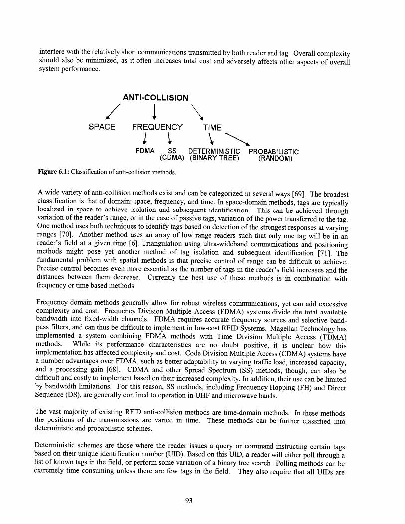
interfere with the relatively short communications transmitted by both reader and tag. Overall complexityshould also be minimized, as it often increases total cost and adversely affects other aspects of overallsystem performance.
ANTI-COLLISION
SPACE FREQUENCY TIME
FDMA SS DETERMINISTIC PROBABILISTIC(CDMA) (BINARY TREE) (RANDOM)
Figure 6.1: Classification of anti-collision methods.
A wide variety of anti-collision methods exist and can be categorized in several ways [69]. The broadestclassification is that of domain: space, frequency, and time. In space-domain methods, tags are typicallylocalized in space to achieve isolation and subsequent identification. This can be achieved throughvariation of the reader's range, or in the case of passive tags, variation of the power transferred to the tag.One method uses both techniques to identify tags based on detection of the strongest responses at varyingranges [70]. Another method uses an array of low range readers such that only one tag will be in anreader's field at a given time [6]. Triangulation using ultra-wideband communications and positioningmethods might pose yet another method of tag isolation and subsequent identification [71]. Thefundamental problem with spatial methods is that precise control of range can be difficult to achieve.Precise control becomes even more essential as the number of tags in the reader's field increases and thedistances between them decrease. Currently the best use of these methods is in combination withfrequency or time based methods.
Frequency domain methods generally allow for robust wireless communications, yet can add excessivecomplexity and cost. Frequency Division Multiple Access (FDMA) systems divide the total availablebandwidth into fixed-width channels. FDMA requires accurate frequency sources and selective band-pass filters, and can thus be difficult to implement in low-cost RFID Systems. Magellan Technology hasimplemented a system combining FDMA methods with Time Division Multiple Access (TDMA)methods. While its performance characteristics are no doubt positive, it is unclear how thisimplementation has affected complexity and cost. Code Division Multiple Access (CDMA) systems havea number advantages over FDMA, such as better adaptability to varying traffic load, increased capacity,and a processing gain [68]. CDMA and other Spread Spectrum (SS) methods, though, can also bedifficult and costly to implement based on their increased complexity. In addition, their use can be limitedby bandwidth limitations. For this reason, SS methods, including Frequency Hopping (FH) and DirectSequence (DS), are generally confined to operation in UHF and microwave bands.
The vast majority of existing RFID anti-collision methods are time-domain methods. In these methodsthe positions of the transmissions are varied in time. These methods can be further classified intodeterministic and probabilistic schemes.
Deterministic schemes are those where the reader issues a query or command instructing certain tagsbased on their unique identification number (UID). Based on this UID, a reader will either poll through alist of known tags in the field, or perform some variation of a binary tree search. Polling methods can beextremely time consuming unless there are few tags in the field. They also require that all UIDs are
~ 4
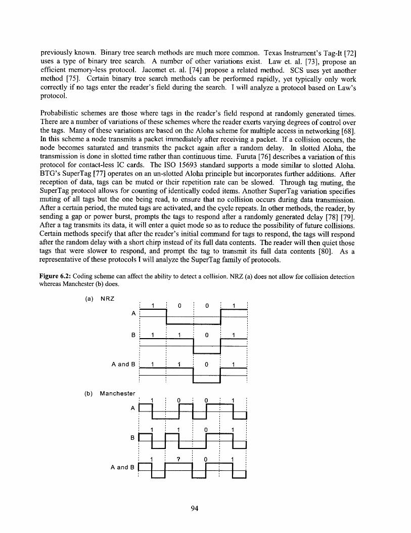
previously known. Binary tree search methods are much more common. Texas Instrument's Tag-It [72]uses a type of binary tree search. A number of other variations exist. Law et. al. [73], propose anefficient memory-less protocol. Jacomet et. al. [74] propose a related method. SCS uses yet anothermethod [75]. Certain binary tree search methods can be performed rapidly, yet typically only workcorrectly if no tags enter the reader's field during the search. I will analyze a protocol based on Law'sprotocol.
Probabilistic schemes are those where tags in the reader's field respond at randomly generated times.There are a number of variations of these schemes where the reader exerts varying degrees of control overthe tags. Many of these variations are based on the Aloha scheme for multiple access in networking [68].In this scheme a node transmits a packet immediately after receiving a packet. If a collision occurs, thenode becomes saturated and transmits the packet again after a random delay. In slotted Aloha, thetransmission is done in slotted time rather than continuous time. Furuta [76] describes a variation of thisprotocol for contact-less IC cards. The ISO 15693 standard supports a mode similar to slotted Aloha.BTG's SuperTag [77] operates on an un-slotted Aloha principle but incorporates further additions. Afterreception of data, tags can be muted or their repetition rate can be slowed. Through tag muting, theSuperTag protocol allows for counting of identically coded items. Another SuperTag variation specifiesmuting of all tags but the one being read, to ensure that no collision occurs during data transmission.After a certain period, the muted tags are activated, and the cycle repeats. In other methods, the reader, bysending a gap or power burst, prompts the tags to respond after a randomly generated delay [78] [79].After a tag transmits its data, it will enter a quiet mode so as to reduce the possibility of future collisions.Certain methods specify that after the reader's initial command for tags to respond, the tags will respondafter the random delay with a short chirp instead of its full data contents. The reader will then quiet thosetags that were slower to respond, and prompt the tag to transmit its full data contents [80]. As arepresentative of these protocols I will analyze the SuperTag family of protocols.
Figure 6.2: Coding scheme can affect the ability to detect a collision. NRZ (a) does not allow for collision detectionwhereas Manchester (b) does.
(a) NRZ1 0:0 1
A
B 1 1 0 1
A and B
(b) Manchester
A
B
1 0 0 1
110 1
A and 0A and BZ
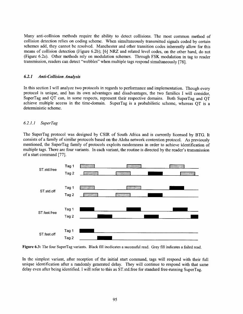
Many anti-collision methods require the ability to detect collisions. The most common method ofcollision detection relies on coding scheme. When simultaneously transmitted signals coded by certainschemes add, they cannot be resolved. Manchester and other transition codes inherently allow for thismeans of collision detection (Figure 6.2b); [6] NRZ and related level codes, on the other hand, do not(Figure 6.2a). Other methods rely on modulation schemes. Through FSK modulation in tag to readertransmission, readers can detect "wobbles" when multiple tags respond simultaneously [78].
6.2.1 Anti-Collision Analysis
In this section I will analyze two protocols in regards to performance and implementation. Though everyprotocol is unique, and has its own advantages and disadvantages, the two families I will consider,SuperTag and QT can, in some respects, represent their respective domains. Both SuperTag and QTachieve multiple access in the time-domain. SuperTag is a probabilistic scheme, whereas QT is adeterministic scheme.
6.2.1.1 SuperTag
The SuperTag protocol was designed by CSIR of South Africa and is currently licensed by BTG. Itconsists of a family of similar protocols based on the Aloha network contention protocol. As previouslymentioned, the SuperTag family of protocols exploits randomness in order to achieve identification ofmultiple tags. There are four variants. In each variant, the routine is directed by the reader's transmissionof a start command [77].
Tag 1ST.std.free
Tag 2
ST.std.off
ST.fast.free
ST.fast.off
Tag 1
Tag 2
Tag 1
Tag 2
Tag 1
Tag 2
Figure 6.3: The four SuperTag variants. Black fill incdicates a successful read. Grey fill indicates a failed read.
In the simplest variant, after reception of the initial start command, tags will respond with their fullunique identification after a randomly generated delay. They will continue to respond with that samedelay even after being identified. I will refer to this as ST.std.free for standard free-running SuperTag.
[I
J ] _ | _ _ __
I
I
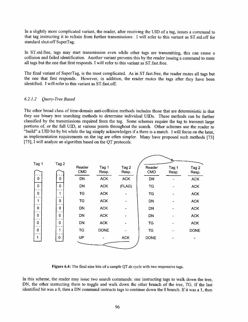
In a slightly more complicated variant, the reader, after receiving the UID of a tag, issues a command tothat tag instructing it to refrain from further transmissions. I will refer to this variant as ST.std.off forstandard shut-off SuperTag.
In ST.std.free, tags may start transmission even while other tags are transmitting, this can cause acollision and failed identification. Another variant prevents this by the reader issuing a command to muteall tags but the one that first responds. I will refer to this variant as ST.fast.free.
The final variant of SuperTag, is the most complicated. As in ST.fast.free, the reader mutes all tags butthe one that first responds. However, in addition, the reader mutes the tags after they have beenidentified. I will refer to this variant as ST.fast.off.
6.2.1.2 Query-Tree Based
The other broad class of time-domain anti-collision methods includes those that are deterministic in thatthey use binary tree searching methods to determine individual UIDs. These methods can be furtherclassified by the transmissions required from the tag. Some schemes require the tag to transmit largeportions of, or the full UID, at various points throughout the search. Other schemes use the reader to"build" a UID bit by bit while the tag simply acknowledges if a there is a match. I will focus on the later,as implementation requirements on the tag are often simpler. Many have proposed such methods [73][75], I will analyze an algorithm based on the QT protocols.
Tag
O0
0
0
1
0
0
0
0I.
Tag 2
0
0
0
0
0
0
1
0
F Tag 1Resp.
ACK
ACK
ACK
ACK
ACK
ACK
ACK
DONE
Tag 2Resp.
ACK
(FLAG)
ACK
ReaderCMD
DN
TG
TG
DN
DN
DN
TG
TG
DONE
Tag 1Resp.
Tag 2Resp.
ACK
ACK
ACK
ACK
ACK
ACK
ACK
DONE
Figure 6.4: The final nine bits of a sample QT.ds cycle with two responsive tags.
In this scheme, the reader may issue two search commands: one instructing tags to walk down the tree,DN, the other instructing them to toggle and walk down the other branch of the tree, TG. If the lastidentified bit was a 0, then a DN command instructs tags to continue down the 0 branch. If it was a 1, then
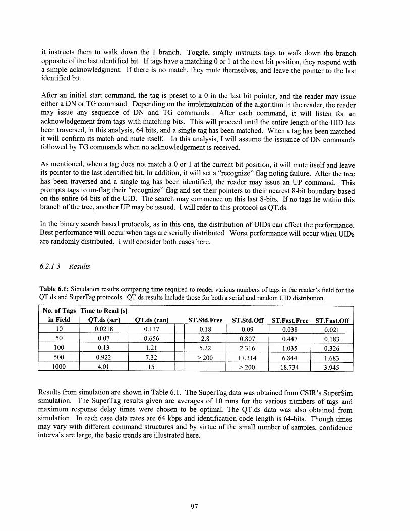
it instructs them to walk down the 1 branch. Toggle, simply instructs tags to walk down the branchopposite of the last identified bit. If tags have a matching 0 or 1 at the next bit position, they respond witha simple acknowledgment. If there is no match, they mute themselves, and leave the pointer to the lastidentified bit.
After an initial start command, the tag is preset to a 0 in the last bit pointer, and the reader may issueeither a DN or TG command. Depending on the implementation of the algorithm in the reader, the readermay issue any sequence of DN and TG commands. After each command, it will listen for anacknowledgement from tags with matching bits. This will proceed until the entire length of the UID hasbeen traversed, in this analysis, 64 bits, and a single tag has been matched. When a tag has been matchedit will confirm its match and mute itself. In this analysis, I will assume the issuance of DN commandsfollowed by TG commands when no acknowledgement is received.
As mentioned, when a tag does not match a 0 or 1 at the current bit position, it will mute itself and leaveits pointer to the last identified bit. In addition, it will set a "recognize" flag noting failure. After the treehas been traversed and a single tag has been identified, the reader may issue an UP command. Thisprompts tags to un-flag their "recognize" flag and set their pointers to their nearest 8-bit boundary basedon the entire 64 bits of the UID. The search may commence on this last 8-bits. If no tags lie within thisbranch of the tree, another UP may be issued. I will refer to this protocol as QT.ds.
In the binary search based protocols, as in this one, the distribution of UIDs can affect the performance.Best performance will occur when tags are serially distributed. Worst performance will occur when UIDsare randomly distributed. I will consider both cases here.
6.2.1.3 Results
Table 6.1: Simulation results comparing time required to reader various numbers of tags in the reader's field for theQT.ds and SuperTag protocols. QT.ds results include those for both a serial and random UID distribution.
No. of Tags Time to Read [s]in Field QT.ds (ser) QT.ds (ran) ST.Std.Free ST.Std.Off ST.Fast.Free ST.Fast.Off
10 0.0218 0.117 0.18 0.09 0.038 0.02150 0.07 0.656 2.8 0.807 0.447 0.183100 0.13 1.21 5.22 2.316 1.035 0.326500 0.922 7.32 > 200 17.314 6.844 1.6831000 4.01 15 > 200 18.734 3.945
Results from simulation are shown in Table 6.1. The SuperTag data was obtained from CSIR's SuperSimsimulation. The SuperTag results given are averages of 10 runs for the various numbers of tags andmaximum response delay times were chosen to be optimal. The QT.ds data was also obtained fromsimulation. In each case data rates are 64 kbps and identification code length is 64-bits. Though timesmay vary with different command structures and by virtue of the small number of samples, confidenceintervals are large, the basic trends are illustrated here.
6.2.1.4 Comparison
These two classes of protocols can be compared on two grounds - performance and implementation. Inregards to performance, we should note, in particular, identification rates, and relative behavior withvarying numbers of tags in the interrogation range. Performance in the presence of noise and otherunique advantages and disadvantages should also be considered. Regarding implementation, requiredcircuitry and commands are particularly important. I will discuss the SuperTag and QT protocols onthese terms.
In examining the SuperTag protocols alone, we notice the increase in linearity as we move fromST.std.free to Std.fast.off. This is due to the additional functions which either shut-off tags after theyhave been identified, and/or mutes tags while one is transmitting. Both of these functions have the affectof reducing the number of responding tags in the field and hence increase linearity. We see thatST.fast.off is essentially linear with the number of tags in the field.
In examining the QT.ds protocol, we notice the marked difference in performance for a serial versusrandom distribution of numbers. In certain applications such as those in factories or distribution centers,UIDs may very well be serially distributed. In other applications such as in store check-out lines, theymay be randomly distributed. Both cases should be considered. In the SuperTag protocols there will beno difference with the distribution of codes. Also, we note that the QT.ds protocol is linear with thenumber of tags in the field for a random distribution of UIDs. We also note that as the number of tags inthe field nears the "group" capacity of 256 tags (by virtue of the 8-bit UP), the number of tags read persecond increases. This explains the non-linearities seen for a serial distribution of UIDs.
Noting the performance between the two protocols, performance is similar for low numbers of tags in thefield. As the numbers increase, the non-linearites become exposed. Required commands transmitted bythe reader should also be considered. Of all the SuperTag protocols and the QT.ds protocol theST.std.free will likely require the least amount of signaling from the reader. In certain frequency bandswith tight limits, this attribute may be useful. The directed search of the QT.ds protocol requires asignificant amount of signaling, as does the ST.fast.off protocol. In general, the more signaling, the morebandwidth, and the higher the probability that an error may occur.
Beyond performance and commands, implementation is important. The SuperTag protocols require somemeans of generating a random delay before responding. This requires some form of random numbergenerator. Many implementations may be possible, some more complex than others. Some havesuggested using the tolerance inherent in circuit components as a means of generating a random number[80]. Others may use a form of oscillator. The more advanced SuperTag protocols must also be able torecognize the commands to shut off and mute. The QT.ds protocol requires some form of comparator tocompare the transmitted bit with the bit stored in memory. They must also maintain pointers to bits andsome state information. In any case, excessive circuitry leads to more area on the chip and higher cost.
The QT.ds and SuperTag protocols each have their own unique advantages and disadvantages. TheQT.ds protocol has the inherent ability to select tags with particular UIDs. This can be useful inapplications where specific tags or groups of tags may need to be addressed or ignored. The SuperTagprotocols, at least he ST.std.off, require fewer transmissions from the reader, reducing bandwidth andprobability for error. A unique disadvantage of the QT.ds protocol and other binary search schemes isthat tags arriving during the search may not be included in the deductions. Depending on implementation,however, this may not be a problem. A problem with the SuperTag protocols and other related randomresponse protocols is the requirement of specifying a maximum delay time. This must either be
transmitted to the tag or preset at manufacture. The effect will vary depending on the number of tags inthe field.
6.2.2 Channelization
Depending on the implementation and band of operation, anti-collision schemes may be "channelized" infrequency, time, and space, or a combination of all three. This can achieve improved identification rates.It also, however, can complicate the system and increase probabilities of error.
6.2.3 System Considerations
The performance of the individual protocol is important, however, it is the overall system level resultwhich is most important. With a well chosen identification coding scheme, and an anti-collision protocolthat allows addressing of particular codes or groups of codes, much of the anti-collision can in fact bemoved off the tag into the host or reader. For example, in certain situations large portions of theidentification code may be already known, or it may be desired to only identify tags with particular codes.In such situations, the reader can directly address the tags with those codes. Deterministic protocols allowthis; most probabilistic schemes, however, do not.
6.3 Commands
There are generally two classes of RFID systems in regards to commands and protocols: tag talks first(TTF) and reader talks first (RTF). In TTF systems, tags respond as soon as sufficiently powered. InRTF systems, tags initialize to a muted state. They only respond unless commanded by the reader to doso. RTF methods are preferred largely because they inherently prevent interference from incompatibletags. For example, in an area with tags of two different vendors, by virtue of their having different startcommands, only the tags compatible with the reader will understand the command and respond. If bothtags were TTF, they may respond simultaneously and interfere with each other's communications.
Commands, like anti-collision protocols, influence both performance and implementation. Morecommands may mean greater performance, but would likely require more circuitry. At the very least, thecommand set should include a start command, and those commands necessary to run the anti-collisionprotocol and achieve the necessary performance. Issues in performance of particular importance includeidentification rate and data integrity.
Additional commands may be necessary for additional applications and functionality. For ultimate low-cost read-only tags though, the only functionality should be to successfully transmit the identificationcode.
6.3.1 Commands and Bandwidth
As we saw in the discussion on coding and modulation, the probability of transmitting a component of asignal, say zero amplitude for a given clock period versus full amplitude for half of a clock periodfollowed by zero amplitude for the second half of a clock period, will affect the bandwidth of a signal. Ifthe probability of transmitting no modulations is higher than the probability of transmitting half period
modulations, the bandwidth will be lower. This effect is most useful when considering the reader, as itssignal power is maximized to meet field strength and power regulations. Consequently its coding,modulation, and transmissions will be limited by bandwidth regulations. In situations where bandwidthrelative to power is very limited, this must be considered.
6.4 Summary
In this chapter we have considered the issues related to command protocols and anti-collision algorithms.As the goal in passive RFID systems is simply to read the identification codes stored on the tag, andmultiple tags will be present in the interrogation range of a reader, command protocols should beoptimized around the anti-collision protocols. In considering anti-collision protocols, important issues arenot only identification rates, but also required command set, performance in the presence of noise, andimplementation details. In addition, affects on bandwidth can also be extremely important.
100
I
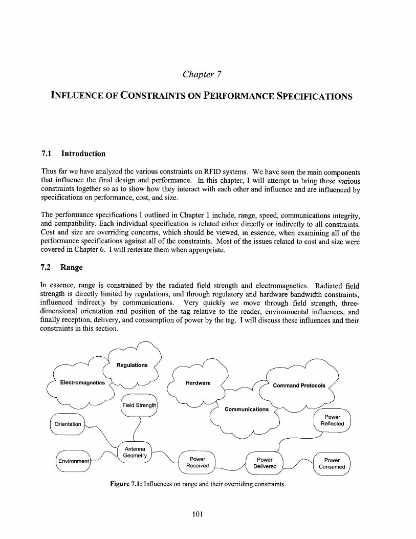
Chapter 7
INFLUENCE OF CONSTRAINTS ON PERFORMANCE SPECIFICATIONS
7.1 Introduction
Thus far we have analyzed the various constraints on RFID systems. We have seen the main componentsthat influence the final design and performance. In this chapter, I will attempt to bring these variousconstraints together so as to show how they interact with each other and influence and are influenced byspecifications on performance, cost, and size.
The performance specifications I outlined in Chapter 1 include, range, speed, communications integrity,and compatibility. Each individual specification is related either directly or indirectly to all constraints.Cost and size are overriding concerns, which should be viewed, in essence, when examining all of theperformance specifications against all of the constraints. Most of the issues related to cost and size werecovered in Chapter 6. I will reiterate them when appropriate.
7.2 Range
In essence, range is constrained by the radiated field strength and electromagnetics. Radiated fieldstrength is directly limited by regulations, and through regulatory and hardware bandwidth constraints,influenced indirectly by communications. Very quickly we move through field strength, three-dimensional orientation and position of the tag relative to the reader, environmental influences, andfinally reception, delivery, and consumption of power by the tag. I will discuss these influences and theirconstraints in this section.
Figure 7.1: Influences on range and their overriding constraints.
101
7.2.1 Field Strength, Orientation, and the Environment
Range is often specified as a maximum quantity; however, this has use to only limited applications. Inmany applications, location and orientation will be relatively unconstrained. We saw in Chapter 2 thatfield strengths are highly orientation and location dependent. Depending on the geometry of the antenna,radiation/field patterns can vary radically. For example, very directional antennas can be constructed atboth near-field frequencies and far-field frequencies. At the near-field frequencies, ferrite can beincorporated into the core of the coil, whereas in the far-field, antennas can be made more directionalthrough arrays or more advanced geometries. With such directional patterns, greater range can beachieved for a given power radiated; yet the readable locations are obviously far more limited. Someapplications may require highly directional characteristics whereas others may require omni-directionalcharacteristics.
If regulations were to simply specify the maximum radiated power (i.e. EIRP), then highly directionalantennas could be used. Limits, however, are typically imposed at maximum field strengths at certaindistances or antenna input powers and antenna gains. Such is the case, in truth, with regulations of mostadministrations. Under certain administrations, however, at certain frequencies, more highly directionalantennas may be used. For example, for frequency hopping use at 902 MHz, 2.45 GHz, and 5.8 GHz inthe United States, radiated power is specified in terms of antenna input power and antenna gain. It isalso specified that antenna gain may be increased above the specified limit, but that antenna input powermust then be reduced by the same factor, effectively establishing a limit on field strength and powerdensity at a given distance, or EIRP/ERP. The situation in Europe is similar for these frequencies - therelimits are expressed in terms of ERP or EIRP. In Japan, however, limits are typically imposed directly onthe antenna gain and input power. Though there is an associated EIRP, one must not increase the antennagain or input power above the specified limit. In cases where limits are on EIRP, though allowable,increased directionality will not help increase the maximum range. It will however limit the size of theinterrogation field, meaning perhaps less interference, fewer tags in the field, and likely more efficientanti-collision. A directional pattern, along with controlled variations of field strength and power (belowregulations), allows a further degree of freedom in controlling the field spatially, possibly allowing forimproved anti-collision.
Thus, we see that regulations essentially determine field strength and power density at a specific location,even though the electromagnetics allows tremendous flexibility. A problem, however, is that regulatorymeasurements of field strength and power densities at certain distances are maximum levels. Once areader is placed in an unconstrained environment with surrounding conductors, patterns can changetremendously. This affect must be taken into account when considering specific applications andconfigurations.
7.2.2 Power Reception, Delivery, and Consumption
Given some field strength or power density at a specific location, the problem next becomes receivingpower. For maximum induced voltage and supplied power, the tag's antenna must be oriented optimallyto the transmitted field. This, of course, depending on the application, may be an extremely difficult task.Perhaps if tagged objects are moving by on a conveyor in constrained orientations, maximum availablepower may be received. For many applications, however, this will not be the case. Depending on thegeometry and characteristics of the tag's antenna, the tag will be more or less sensitive to orientation. Inaddition, just as reader antennas may incorporate directionality, so to can tag antennas. Special antennaconfigurations such as orthogonal loops, can be used to reduce orientation nulls; however, orientationconsiderations must still be carefully weighed on the basis of the application and configuration.
102
Field strength and power density at a location is determined by regulations and environmental factors.Field strength and power density available for capture by a tag is affected by its antenna geometry andorientation. Given some antenna geometry and orientation, the power delivered to the tag's circuitrybecomes a function of the tags circuit parameters. Impedance of antennas, matching circuits, and loadsare particularly important. Together, they determine current through the various portions of the circuitbased on an induced voltage. Induced voltage can be maximized by using various techniques specific tothe frequency of operation.
In the near-field and far-field, different techniques are used. With a reactive link, the tag acts as a sink.Through resonance at both the tag's and reader's antennas, the tag can, in a sense, widen its drain. Theuse of resonance, by combining a capacitor in parallel with the coil of an inductive tag, and combining acapacitor in series with the coil of an inductive reader, can establish a high quality factor. The impedanceof the combined resonant circuit and the equivalent impedance of the rest of the tag's circuitry determinethis quality factor. The quality factor is defined as both the ratio of energy stored to energy dissipated,and the ratio of center frequency to 3 dB bandwidth. Thus, through this quality factor there is anassociated filter. This filter is either equivalent to or narrower than the filter of the tag's antenna itself.At high quality factors, bandwidth is narrow and care must be taken not to filter out information. Wehave seen that modulation, or the imparting of information onto a carrier signal, creates sidebands. If wefilter these out, we lose information. High quality factors also create sensitivity to environmentalinfluences. Surrounding antennas or metals can change the resonant frequency and effectively shift the Qfilter of center. In situations where tags will be collocated with other tags, a common strategy is to tunetags to higher than the nominal frequency of operation.
In the far field, the situation is different. Power delivered to a load is determined by the degree ofmatching between the antenna impedance and the equivalent impedance of the rest of the circuit. If thereis a conjugate match between these two impedances, meaning the real portions are equal and the reactiveportions are equal and opposite, maximum power will be delivered. If there is a mismatch, power will bereflected in the circuit and re-radiated by the antenna. This, of course, is the basis of backscattermodulation (Chapter 2). Controlled variation of the load impedance causes controlled modulations of theincident carrier signal. The more power scattered, the less absorbed. The more power absorbed, the lessscattered.
Given some power delivered the load, it next becomes important how the "load" is configured. Thepower delivered is used not only for powering the tag, but also for providing information, a clock, and theestablishment of biasing. Regarding configuration of the load, diodes are necessary to rectify the signalfor both power supply and information extraction. Energy is stored, managed, and delivered to thedigital circuitry. In the digital circuitry, the decision-making occurs. After reception and processing,typically through envelope detection, functions are performed and decisions are made based on theinformation. Tags may compare received information with stored information, decide to transmit storedinformation, mute themselves, or any number of other functions. These functions, in turn, require power.Power consumption is determined through the activity of the individual gates, the capacitance associatedwith the integrated circuit, and the supply voltage. The gate activity is determined by clock frequencyand demands placed largely by anti-collision functions. These circuits also have an associated thresholdvoltage below which they will not function. The power delivered to the load must provide this thresholdvoltage and power necessary to allow the tag to achieve its functions. If these functions cannot beperformed, the tag must be moved closer to the field source where field strength and power will increaserelative to distance.
It is not just power delivered for powering the tag that is important, but also power available for detection.If there is not a suitable difference in signal levels, a clearly defined decision threshold, or low signal
103
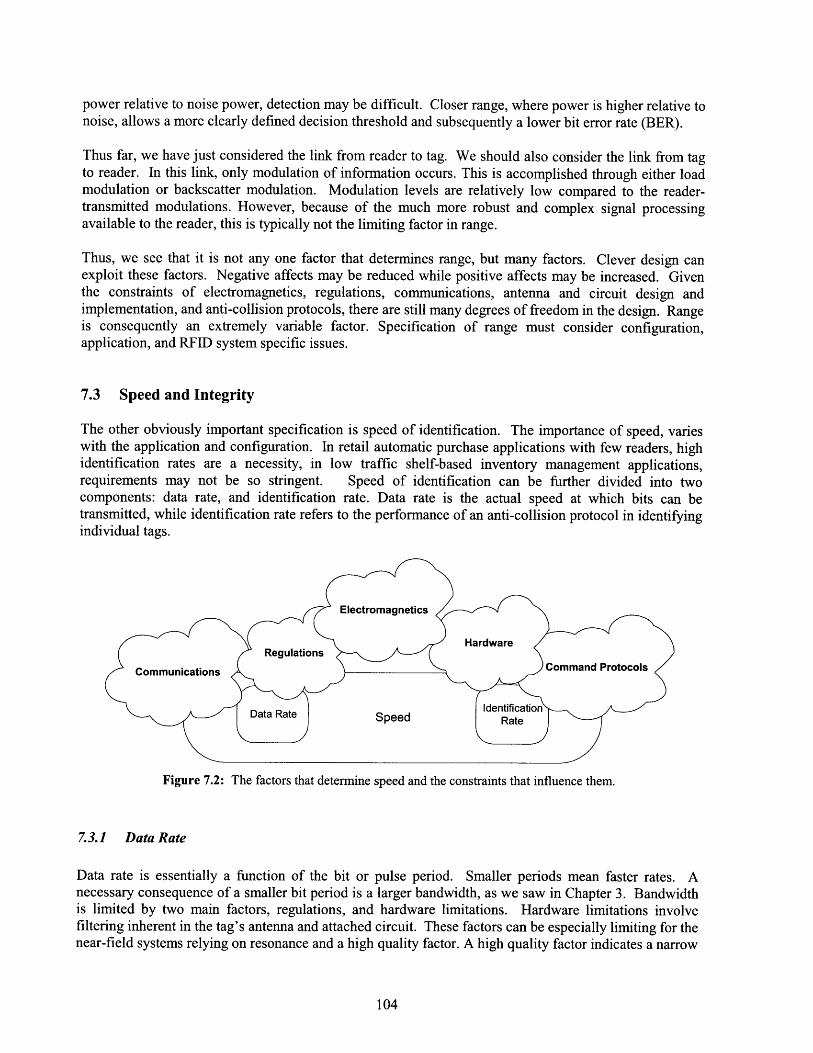
power relative to noise power, detection may be difficult. Closer range, where power is higher relative tonoise, allows a more clearly defined decision threshold and subsequently a lower bit error rate (BER).
Thus far, we have just considered the link from reader to tag. We should also consider the link from tagto reader. In this link, only modulation of information occurs. This is accomplished through either loadmodulation or backscatter modulation. Modulation levels are relatively low compared to the reader-transmitted modulations. However, because of the much more robust and complex signal processingavailable to the reader, this is typically not the limiting factor in range.
Thus, we see that it is not any one factor that determines range, but many factors. Clever design canexploit these factors. Negative affects may be reduced while positive affects may be increased. Giventhe constraints of electromagnetics, regulations, communications, antenna and circuit design andimplementation, and anti-collision protocols, there are still many degrees of freedom in the design. Rangeis consequently an extremely variable factor. Specification of range must consider configuration,application, and RFID system specific issues.
7.3 Speed and Integrity
The other obviously important specification is speed of identification. The importance of speed, varieswith the application and configuration. In retail automatic purchase applications with few readers, highidentification rates are a necessity, in low traffic shelf-based inventory management applications,requirements may not be so stringent. Speed of identification can be further divided into twocomponents: data rate, and identification rate. Data rate is the actual speed at which bits can betransmitted, while identification rate refers to the performance of an anti-collision protocol in identifyingindividual tags.
Figure 7.2: The factors that determine speed and the constraints that influence them.
7.3.1 Data Rate
Data rate is essentially a function of the bit or pulse period. Smaller periods mean faster rates. Anecessary consequence of a smaller bit period is a larger bandwidth, as we saw in Chapter 3. Bandwidthis limited by two main factors, regulations, and hardware limitations. Hardware limitations involvefiltering inherent in the tag's antenna and attached circuit. These factors can be especially limiting for thenear-field systems relying on resonance and a high quality factor. A high quality factor indicates a narrow
104
bandwidth and thus an upper bound on the data rate. Far-field system tag antennas also have anassociated bandwidth. These hardware limitations are typically not as constraining as regulations,however.
Data rate is not necessarily a function of operating frequency, but rather the bandwidth available byregulations at that frequency, and further by the bandwidth limitations on the sidebands. By virtue of theorganization of the spectrum, there is generally more available bandwidth at higher frequencies.Operating frequency typically defines the derivation source of the tags circuit clock frequency. At thenear-field frequencies, tags are typically synchronous and the clock on the tag is typically divided directlyfrom the carrier frequency. At far-field frequencies, tags typically derive the clock from a reader-transmitted modulation. Some systems my incorporate phase locked loops and oscillators, while othersmay constantly use an edge of the reader transmitted pulse to continuously define the clock. In any case,regardless of derivation, a faster clock means faster processing, yet increased power consumption. Thus,clocks are typically divided down to similar rates between both near-field and far-field systems. It is thebandwidth, thus, that determines speed. More particularly, in RFID systems, it is the bandwidth of thereader's signal that determines data rate of the reader to tag transmission, and depending on configuration,the data rate of the tag's clock and transmissions back to the reader.
Bandwidth is typically given by the main channel frequency span. There is also a single, or multipleassociated sideband levels. Depending on the administration and operating frequency, regulations aredefined differently. If we consider Europe's regulations at 13.56 MHz, the main channel bandwidth isgiven by the ISM designation of +/- 7 kHz. Sidebands are given at two levels. A level less than the mainband limit, but higher than the lowest level, extends to +/- 150 kHz. Outside of this band is a furtherreduced strength level where general spurious emissions are allowed. In the US, there is simply the ISMdesignated +/- 7 kHz, and a low field strength level designated for general emissions. Japan further uses adifferent method. There, bandwidth is given as 7 times the bit rate. These regulatory issues are, ofcourse, not only directly related to speed, but compatibility.
We should also consider the bandwidth of tag-modulated signals. Because the field strength levels ofthese signals are significantly lower than those of readers, they fall below regulatory limits. Bandwidthfrom the tag to the reader is thus limited by hardware considerations. Because readers are stationary, theymay operate at the maximum capacity allowed by their administration, yet different coding andmodulation schemes may be necessary to achieve similar performance between the different regions.Such is an approach adopted by some manufacturers. If tags cannot easily detect both methods, thispresents a problem for compatibility.
We saw in Chapter 3 how coding and modulation influences bandwidth and bit rate. Further we saw thatcertain codes allow signals that contain more energy than others. In the link from reader to tag, a signalthat contains more energy is desirable, as it not only must carry information, but also power. Thus, in thisrespect, speed and range are coupled. If hardware considerations were of concern, we should note that fora given coding and modulation scheme, increasing the bit rate would result in an increase in bandwidth.Given the hardware bandwidth limitations, this would result in less power to the tag. This representsfurther coupling between speed and range.
7.3.2 Identification Rate
Given some bit rate, the anti-collision protocol becomes important for determining speed. Essentially itdefines a tag identification rate per bit rate efficiency. Given a bit rate R, and a identification rate, T, wecan define the protocol efficiency by
105
T tags
E bits (7.1)
The better anti-collision schemes will have a higher efficiency. Anti-collision protocols, of course,influence the hardware design, which, in turn, noticeably affect cost. This is an important tradeoff -identification rate, versus cost. In addition, they affect power consumption - the greater activitydemanded, the more power consumed. As noted in Chapter 6, there are three domains and several typesof anti-collision within those domains. For-low cost passive RFID systems, the most suitable are those inthe time domain where tags are either identified deterministically based on identification code, orprobabilistically through random response times. Each has their inherent advantages and disadvantages asoutlined. One important advantage of deterministic schemes is the ability to, in essence, move the anti-collision to the reader, host, and associated infrastructure by incorporation of intelligence in these units.Depending on the application and configuration, particular tags may need to be identified. Deterministicschemes can selectively limit this identification. Probabilistic schemes typically don't have this inherentadvantage. They may include it, but only at the cost of extra devices on chip, extra complexity, size, andcost.
It also should be noted that anti-collision schemes can affect the data rate of the transmissions. Thoserequiring infrequent transmissions from the reader will have a lower associated bandwidth and thus mayincrease their data rate. Probabilistic schemes may have an advantage in this arena as they may requirefewer transmissions from the reader. Closely related to anti-collision scheme is the integrity of thetransmissions. The reader to tag fidelity is higher due to the much greater signal level. Tag to readerfidelity is much lower, and thus those protocols that require fewer transmissions from the tag to readermay be more reliable. As detailed in Chapter 4, some schemes allow only simple acknowledgementsfrom the tag. This too, though, has its problems, as an error on this response means a failed transmission.
Data integrity is strongly related to both range and speed. Error detection or correction may beimplemented; however this can reduce speed, require more complex hardware, require more powerconsumption, and hence reduce range. As mentioned previously the closer to the reader, the greater thefield strength, a more easily discernable signal, and hence increased data integrity.
Thus we have seen that both data rate and anti-collision schemes affect the speed of operation. Anti-collision also affects the data rate. Both the anti-collision scheme and the data rate in combination withthe coding and modulation scheme affect the power consumption of the tag. This of course, affects therange as discussed previously. Both data rate and anti-collision are additionally extremely important onthe basis of data integrity and compatibility with worldwide regulations.
7.4 Compatibility and Standardization
As mentioned in the introduction, compatibility between different regulatory administrations, andbetween RFID systems of different vendors is important for the continued adoption and proliferation ofRFID. I have dealt with the regulatory issues above. Here I will outline some of the important concernsrelated to standardization for compatibility between RFID systems of different vendors.
In general, there are two approaches one can take with respect to RFID standardization. Systems may becompletely incompatible and orthogonal in coding, modulation, and commands and protocols. Or, theymay be completely compatible. In either case, the reader-talks-first systems are recommended as tagsdefault to a mute state and are only activated when specifically commanded by the reader. If these startcommands are completely different and the probability of either inadvertently transmitting the command
106
-----------. ~
is low, either through different coding and modulation schemes, or a start command of sufficient length,then one need not worry about the additional protocols of the system. Tags will simply not interfere. If itis desired that a reader communicate with both types of tags, then the reader should accommodate forboth coding and modulation schemes, and associated command protocols. Systems that are completelycompatible must have identical coding and modulation schemes and command protocols. Certaincommands may be omitted from certain tags, yet if omitted, they must be ignored.
Both incompatible and compatible methods for achieving compatibility, or, in essence, lack ofinterference, are feasible. Incompatible methods allow complete freedom of design to different vendors,yet complicate matters for the end user. If one wishes to have a reader capable of reading tags of multiplevendors, they must install readers capable of the different schemes and protocols. This can be morecostly, yet with advances in software-defined radio and signal processing, this is becoming less of anissue. Further, some end users may only wish to read tags of a particular vendor. In this case theincompatible method does not present a problem. The compatible method allows for inexpensive readersand simplicity for the end users, yet impose stringent constraints on the designer. Innovation can belimited, and competition leading to decreased costs, product differentiation, and further innovation can befurther harmfully limited.
Operating frequency is another important issue related to compatibility. Obviously those tags operating atdifferent frequencies are completely orthogonal and present virtually no chance of interference.However, for end users desiring to read tags at multiple frequencies, readers must additionally have thiscapability. There have been efforts to designate frequencies for particular standards, however this is notrecommended. Electromagnetic field and wave behavior at a given frequency can differ drasticallydepending on the environment for a given application. A given frequency may very well work flawlesslyin one situation, yet in a different situation, even though for the same or similar application, may not workwell. Other frequencies may be more appropriate. Much testing still remains to determine behavior ofsystems operating at different frequencies. Selection of a single frequency, even if for only a singleapplication, may be premature. Decisions of this nature should be made on an application andconfiguration specific basis.
In any regard, standardization for compatibility is a sensitive issue and can have drastic affects on theproliferation and innovation of RFID technology. Achieving compatibility by complete incompatibilitythrough reader talks first systems and completely orthogonal initialization commands, is a viableapproach. Compatibility through complete compatibility may also be an option. Both methods may workin parallel, leaving the choice up to the designer and end user. As each operating frequency has its owninherent advantages and disadvantages in a particular environment, designations of specific frequencies,in general, should not be made.
7.5 Summary
In this chapter we have seen how the important performance specifications are constrained byelectromagnetics, communications, regulations, hardware design, and command protocols. We have seenthat the specifications are dependent both directly and indirectly on all of the fundamental constraints.We have also considered the dependence of these specifications and constraints on applications andconfigurations. Design of tags and standards should reflect the high degree of coupling betweenspecifications, constraints, and desired application and configuration.
107
Chapter 8
CONCLUSION
8.1 Conclusion
In the recent past there has been increased adoption of RFID systems for a variety of applicationsrequiring ever-lower costs. In parallel, there has been increased activity in RFID standards development.Already established standards include those for applications ranging from animal tagging, throughhighway vehicle identification. Currently, there are ongoing efforts to develop standards for itemmanagement and logistics applications. Perhaps the most demanding near term application for itemmanagement is tagging of low cost consumable items. This trend towards tagging such low-cost items ona global scale places stringent demands on the RFID systems themselves. In addition to performancerelated concerns, size, and particularly cost are extremely important. Absolute minimum cost tags are anecessity.
To realize such low cost tags, design must be optimized specifically for this purpose. An understandingof the fundamental constraints on the systems, along with clever design, is imperative. The fundamentalconstraints on these low-cost passive RFID tags include electromagnetics, communications, regulations,and physical implementation. In this thesis I have analyzed these various constraints on the basis of low-cost passive RFID. We have seen how these constraints affect cost, size, and the various importantperformance specifications including range, speed, communications integrity, and compatibility.
With low cost tags, we will see increased adoption, and greater volumes, which will further feeddecreases in cost and a continuation of the cycle. Improvements and innovations in manufacturingtechniques should allow for more efficient production and lower cost. Furthermore, increased adoptionwill likely lead to incorporation of additional functionality, such as inclusion of sensors, actuators, andother more advanced functions. In addition, with increased adoption, we will see the development ofadditional applications exploiting the automatic capture and instant machine knowledge of informationabout objects. Increased automation should proliferate, driving increased productivities and efficiencies.
8.2 Future Work
In studying the fundamental constraints on RFID systems and their current state of development, anumber of areas deserving of future work emerge. I will briefly discuss some of these areas here.
As we have seen, power available to the tag is the limiting factor on its range. Though range is not themost important specification for all applications, it is nevertheless important to many. Currently, readerssupply power to the tag through their transmitted field. Through technologies known as "energyharvesting," energy can be collected from ambient sources. This may allow increased range and cause thelimiting factor on range to be receiver sensitivity for communications. Currently, much work is ongoingin energy harvesting. MEMS transducers that convert mechanical vibrations to electric energy, shoeswhich harvest energy while walked in, and integrated circuitry that converts dissipated heat to electric
108
energy, have all been fabricated [82][83][67]. RFID tags may use similar schemes, or improve collectionof ambient electromagnetic radiation.
In the area of electromagnetics, testing and design for specific environments is an area deserving ofattention. In logistics applications, environments typically include a great deal of metal. As we have seenthis can cause problems in altering field and radiation patterns, and thus affect overall performancesignificantly. Antennas allow many degrees of freedom in their configuration, thus improved geometriesshould be studied.
Though much work has been done in the area of communications related to optimization of coding andmodulation, there are still areas that should be addressed. At most frequencies, there are differences inbandwidth and field strength limitations between different regions. Short of worldwide regulationharmonization, coding, modulation, and filtering techniques, which optimize systems for such operation,should be studied. In addition, design of inexpensive FSK and PSK detectors, and improvements in clockgeneration techniques may be useful. Space and frequency domain anti-collision schemes should also beexamined.
In the area of physical implementation, novel tag antenna structures should be investigated. Fractalantennas may be promising as they can allow for reduced size while maintaining reception and radiationperformance [84]. Study should also be done on exploiting the packaging of tagged objects. Packagingof certain objects may allow for integrated antenna structures or energy storage. Manufacturingtechniques, particularly for fabricating and assembling the entire tag structure, including integrated circuitand antenna, should also be investigated.
Chipless tags, in which there is currently much ongoing work, should continue to be studied. Range,memory and anti-collision techniques, in particular, should be examined.
Though the focus of this thesis has been on tags, there is much to be studied in the area of readers.Reader-to-reader anti-collision techniques, in particular should be examined. As RFID systemsproliferate, reader density will increase and the likelihood of interference between readers willsubsequently increase. Such interference can be especially harmful to the integrity of communications.
Finally, additional functions and new applications should provide a number of interesting and compellingareas of research. Integration of sensing and actuating technology, either through MEMS devices, orsimpler material structures, would be useful to a number of current and likely new applications. Newapplications related to robotics and automation should be studied. The identification code from the tag, incombination with a networked database allows simple perception and instant knowledge.
109
NMI
REFERENCES
[1] Yogesh Joshi, "Information Visibility and Its Effect on Supply Chain Dynamics," M.S. Thesis,Massachusetts Institute of Technology, Cambridge, MA, 2000,<http://auto-id.mit.edu/research/whitepapers.html>.
[2] MIT Auto-ID Center, "The Networked Physical World: Proposals for engineering the nextgeneration of computing, commerce, and automatic-identification," MIT-AUTOID-WH-001, 2000,<http://auto-id.mit.edu/research/whitepapers.html>
[3] Jim Eagle, "RFID: The Early Years 1980-1990,"2001,<http://members.surfbest.net/eaglesnest/rfidhist.htm>
[4] Alfred R. Koelle., Steven W. Depp, Jeremy A. Landt, and Ronald E. Bobbett, "Short-Range PassiveTelemetry by Modulated Backscatter of Incident CW RF Carrier Beam," Biotelemetry, Vol. 3,,Academic Press, New York, pp. 337-340, 1976.
[5] Thierry Roz and Vincent Fuentes, "Using Low Power Transponders and Tags for RFIDApplications," EM Microelectronic Marin SA, Marin, Switzerland, <http://www.emmarin.ch/>.
[6] Klaus Finkenzeller, RFID Handbook, John Wiley and Sons, Inc., New York, 1999.
[7] John R. Tuttle, "Traditional and Emerging Technologies and Applications in the Radio FrequencyIdentification (RFID) Industry," IEEE Radio Frequency Integrated Circuits Symposium, 1997.
[8] S. Shuji, H. Yuzo, A. Dobashi, M. Okumura, and T. Kusuzaki, "Products Lifecycle ManagementSystem Using Radio Frequency Identification Technology," Proceedings of the 7th IEEEInternational Conference on Emerging Technologies and Factory Automation (ETFA), Vol. 2, 1999,pp. 1459-1467.
[9] David L. Brock, "The Electronic Product Code," MIT-AUTOID-WH-002, 2001, <http://auto-id.mit.edu/research/whitepapers.html>.
[10] Peter J. Harrop, Chipless Smart Labels: The Ultimate RFID, IDTechx, Cambridge, UK, 1988.
[1 ] N. Komatsu, T. Kon, H. Mukai, K. Kamigama, "Research and Study of Elementary Technology forAchieving Greater Efficiency in Postal Processing: The Present State of RFID and their Applicationsto Postal Services," IPTP Monthly Report, No. 119, 1998.
[12] David H. Staelin, Ann. W. Morgenthaler, and Jin Au Kong, Electromagnetic Waves, Prentice Hall,New Jersey, 1994.
[13] Warren L. Stutzman and Gary A. Thiele, Antenna Theory and Design, 2 nd ed., John Wiley and Sons,Inc., New York, 1998.
[14] David K. Cheng, Field and Wave Electromagnetics, 2nd ed., Addison-Wesley Publishing Co., NewYork, 1992.
110
[15] Richard Ribon Fletcher, "A Low-Cost Electromagnetic Tagging Technology for WirelessIdentification, Sensing, and Tracking of Objects," M.S. Thesis, Massachusetts Institute ofTechnology, Cambridge, MA, 1997.
[16] IEEE Standard Dictionary of Electrical and Electronics Terms, 3rd ed., ANSI/IEEE Standard 100-1984.
[17] Eugene F. Knott, John F. Shaeffer, and Michael T. Tuley, Radar Cross Section, 2nd ed., ArtechHouse, Boston, 1993.
[18] R. C. Hansen, "Relationships Between Antennas as Scatterers and as Radiators," Proceedings of theIEEE, Vol. 77, No. 5, pp. 659-652, 1989.
[19] Robert Blair Green, "The General Theory of Antenna Scattering," Ph.D. Thesis, The Ohio StateUniversity, Columbus, OH, 1963.
[20] Alan Demers, Scott Elrod, Christopher Kantarjiev, and Edward Richley, "A Nano-Cellular LocalArea Network Using Near-Field RF Coupling," Xerox Corporation, Palo Alto, 1994.
[21] Theodore S. Rappaport, Wireless Communications: Principles and Practice, Prentice Hall, NewJersey, 1996.
[22] Jorgen Bach Andersen, Theodore S. Rappaport, and Susumu Yoshida, 1995, "PropagationMeasurements and Models for Wireless Communications Channels," IEEE CommunicationsMagazine, January, 1995.
[23] John B. Anderson, Digital Transmission Engineering, IEEE Press, New York, 1999.
[24] Leon W. Couch, Digital and Analog Communications Systems, 6th ed., Prentice-Hall, New Jersey,2001.
[25] Joseph L. LoCicero and Bhasker P. Patel, "Line Coding," The Mobile Communications Handbook,Gibson, Jerry D., ed., CRC Press, Boca Raton, Florida, 1999, pp. 6-1 - 6-18.
[26] Hwei P. Hsu, Probability, Random Variables, and Random Processes, McGraw-Hill, New York,1997.
[27] William C. Lindsey, and Marvin K Simon, Telecommunication Systems Engineering, Prentice-Hall,New Jersey, 1973.
[28] R.C. Titsworth and L. R. Welch, "Power Spectra of Signals Modulated by Random andPseudorandom Sequences," Jet Propulsion Laboratory, Pasadena, CA, Technical Report No. 32-140,October 1961.
[29] H. Hecht and A. Guida, "Delay Modulation" Proceedings of the IEEE, Vol. 57., No. 7, July 1969,pp.1314-1316.
[30] E. N. Gilbert, "Capacity of a Burst-Noise Channel," Bell System Technical Journal, Vol. 39, pp.1253-1266, September 1960.
111
[31] E. O. Elliott, "Estimates of Error Rates for Codes on Burst-Error Channels," Bell System TechnicalJournal, Vol. 42, p. 1997, September 1963.
[32] Michele Zorzi and Ramesh R. Rao, "Error Control Strategies for the Wireless Channel," IEEE 5thInternational Conference on Universal Personal Communications, Vol. 2, 1996, pp. 970-974.
[33] J. R. Yee and E. J. Weldon, "Evaluation of the Performance of Error-Correcting Codes on a GilbertChannel," IEEE Transactions on Communications, Vol. COM-43, August 1995, pp. 2316-2323.
[34] Mischa Schwartz, Information, Transmission, Modulation, and Noise, McGraw-Hill, New York,1980.
[35] David Withers, Radio Spectrum Management: Management of the Spectrum and Regulation ofRadio Services, 2nd ed., The Institution of Electrical Engineers, London, 1999.
[36] ITU RR, 1998, Radio Regulations, Vol. 1,. International Telecommuications Union.
[37] ERO, European Radiocommunications Office, <http://www.ero.dk>.
[38] ETSI, European Telecommunications Standards Institute, <http://www.etsi.org>.
[39] FCC, Federal Communications Commission, <http://www.fcc.gov>.
[40] MPT, Ministry of Post and Telecommunications, <http://www.joho.soumu.go.jp>.
[41] ARIB, Association of Radio Industries and Businesses, <http://www.arib.or.jp>.
[42] ITU-R 213/1, Technical and Operating Parameters and Spectrum Requirements for Short-RangeRadiocommunication Devices, 2001.
[43] ITU-R SM.1056, Limitation of Radiation for Industrial, Scientific and Medical (ISM) Equipment,1994.
[44] CEPT 70-03, Relating to the Use of Short Range Devices (SRD), May 2001.
[45] ETSI EN 300330-1 V1.3.1 (2001-04), Electromagnetic Compatibility and Radio Spectrum Matters(ERM); Short Range Devices (SRD); Radio equipment in the frequency range 9 kHz to 25 MHz andinductive loop systems in the frequency range 9 kHz to 30 MHz; Part 1: Technical characteristicsand test methods, 2001.
[46] FCC Part 15, Radio Frequency Devices, 2001.
[47] David Mawdsley, EMC Conducted Emissions Measurement: Detectors... what, why and when?,"Technical Notes from Laplace Instruments, 2001,<http://perso.wanadoo.fr/dicomtech/article_lap_2.htm>.
[48] CISPR 16-1, Specification for Radio Disturbance and Immunity Measuring Apparatus and Methods- Part 1: Radio Disturbance and Immunity Measuring Apparatus, International ElectrotechnicalCommission, 1999.
112
[49] ETSI EN 300220-1 V. 1.3.1 (2000-09), Electromagnetic Compatibility and Radio Spectrum Matters(ERM); Short Range Devices (SRD); Radio equipment to be used in the 25 MHz to 1000 MHzfrequency range with power levels ranging up to 500 mW; Part 1: Technical characteristics and testmethods, 2000.
[50] ETSI EN 300440-1 V.1.3.1 (2000-07), Electromagnetic Compatibility and Radio Spectrum Matters(ERM); Short Range Devices; Radio equipment to be used in the 1 GHz to 40 GHz frequency range;Part 1: Technical characteristics and test methods, 2000.
[51 ] John Bums, Richard Rudd, and Zoran Spasojevic, "Compatibility Between Radiocommunication andISM Systems in the 2.4 GHz Frequency Band," Aegis Systems Limited, 1999.
[52] Acheson Colloids Company, "Product Selection Guide," <http://www.achesoncolloids.com/>.
[53] Ramesh Garg, Prakash Bhartia, Inder Bahl, Apisak Ittipiboon, Microstrip Antenna DesignHandbook, Artech House, Boston, 2000.
[54] D. Friedman, H. Heinrich, D-W. Duan., "A Low-Power CMOS Integrated Circuit for Field-PoweredRadio Frequency Identification Tags," IEEE International Solid-State Circuits Conference, 1997, p.294.
[55] Ulrich Kaiser and Wolfgang Steinhagen, "A Low-Power Transponder IC for High-PerformanceIdentification Systems," IEEE Journal ofSolid-State Circuits, Vol. 30, No. 3, pp. 306-310, March1995.
[56] Stephane Donnay, Philip Pieters, KristofVaesen, Wim Diels, Piet Wambacq, Walter De Raedt, EricBeyne, Marc Engels, and Ivo Bolsens, "Chip-Package Codesign of a Low-Power 5-GHz RF FrontEnd," Proceedings of the IEEE, Vol. 88, No. 10, pp. 1583-1597, October 2000.
[57] M.H. Brodsky, Progress in Gallium Arsenide Semiconductors. Scientific American, pp.68-72,February 1990.
[58] J.D. Meindl, Chips for Advanced Computing. Scientific American, pp. 78-88, October 1987.
[59] Lawrence E. Larson, "Integrated Circuit Technology Options for RFIC's - Present Status and FutureDirections," IEEE Custom Integrated Circuits Conference, 1997, pp. 169-176.
[60] Thomas H. Lee, The Design of CMOS Radio-Frequency Integrated Circuits, Cambridge UniversityPress, Cambridge, UK, 1998.
[61] Agilent AN 1089, "Designing Detectors for RF/ID Tags," Agilent Application Note, 1999.
[62] Paul Horowitz and Winfield Hill, The Art ofElectronics, 2nd ed., Cambridge University Press,Cambridge, UK, 1989.
[63] Eric A. Vittoz, "Micropower IC," Low-Power CMOS Design, Anantha Chandrakasan, RobertBrodersen, ed, IEEE Press, New York, 1998.
[64] Chenming Hu, "Device and Technology Impact on Low Power Electronics," Low Power DesignMethodologies, Kluwer Academic Publishers, Boston, 1996, pp. 21-33.
113
[65] Jan M. Rabaey, Massoud Pedram and Paul Landman, "Introduction," Low Power DesignMethodologies, Kluwer Academic Publishers, Boston, 1996, pp. 1-15.
[66] P. Vanoostende, et al., "Evaluation of the limitations of the simple CMOS power estimation formula:comparison with accurate estimation," Proceedings of the European Workshop on Power and TimingModeling, 1992, pp. 16-25.
[67] Athas, William C., "Energy-Recovery CMOS," Low Power Design Methodologies, KluwerAcademic Publishers, Boston, 1996.
[68] Benny Bing, Broadband Wireless Access, Boston, Kluwer Academic Publishers, MA, 2000.
[69] Peter Hawkes, "Anti-collision and Transponder Selection Methods for Grouped "Vicinity" Cardsand RFID tags," lEE Colloquium on RFID Technology, 1999, pp. 7/1-7/12.
[70] Josef Schuermann, U.S. Patent: System and method for reading multiple RF-ID transponders, PatentNumber: US5500651, March 1996.
[71] Robert Fleming, Cherie Kushner, "Integrated, Low-Power, Ultra-Wideband Transceivers forDistributed Position Location and Communication," Aether Wire & Location, Inc., January 1998,<http://www.aetherwire.com/Aether Wire/TechnicalAbstracts_97.pdf>.
[72] Konstantin O. Aslanidis, Alain Berthon, U.S. Patent: Method for repeating interrogations untilfailing to receive unintelligible responses to identify plurality of transponders by an interrogator,Patent Number: US5929801, July 1999.
[73] Ching Law, Kayi Lee, Kai-Yeung Siu, "Efficient Memoryless Protocol for Tag Identification," InProceedings of the 4 th International Workshop on Discrete Algorithms and Methods for MobileComputing and Communications, August 2000.
[74] Marcel Jacomet, Adrian Ehrsam, Urs Gehrig, "Contactless Identification Device With AnticollisionAlgorithm," IEEE Computer Society, CSCC'99, Conference on Circuits, Systems, Computers andCommunications, 4-8 July 1999 Athens,<http://www.microlab.ch/academics/randd/research/cscc/cscc99.pdf>.
[75] Ronald Walter and Keith Vertrees, U.S. Patent: Method and apparatus for radiofrequencyidentification tags, Patent Number: US5856788, January 1999.
[76] Shigeru Furuta, U.S. Patent: Method and system for identifying and communicating with a pluralityof contactless IC cards, Patent Number: US5698837, December 1997.
[77] EM Microelectronic-Marin SA, P4022: Multi Frequency Contactless Identification Device,<http://www.emmarin.com/pdf/RFID/P4022_C.pdf>.
[78] Microchip Technology Inc., microlD 125 kHz Design Guide,<http://www.microchip.com/Download/lit/pline/rfid/guides/51115e.pdf>.
[79] Donald L. Black, Dale Yornes, U.S. Patent: Method for resolving signals collisions between multipleRFID transponders in a field, Patent Number: US6091319, July 2000.
114
i
[80] Pourang Mahdavi, European Patent: A system and method for communicating with multipletransponders, Patent Number: EP1017005A2, May 2000.
[81] John H. Bowers, John Nelson Daigle, Rade Petrovic, U.S. Patent: Anticollision protocol for readingmultiple RFID tags, Patent Number: US5883582, March 1999.
[82] Scott Meninger, Jose Oscar Mur-Miranda, Rajeevan Amirtharajah, Anantha Chandrakasan andJeffrey Lang, "Vibration-to-Electric Energy Conversion," 1999 International Symposium on Low-Power Electronic Design (ISLPED '99), July 1999, pp. 48-53.
[83] N. S. Shenck and J. A. Paradiso, "Energy Scavenging with Shoe-Mounted Piezoelectrics," IEEEMicro, Vol. 21, No. 3, May-June 2001.
[84] R. Breden and R. J. Langley, "Printed Fractal Antennas," IEE National Conference on Antennas andPropagation, 1999.
115
Related Documents