Debugging Embedded Cores in Xilinx FPGAs 1 ©1989-2016 Lauterbach GmbH Debugging Embedded Cores in Xilinx FPGAs TRACE32 Online Help TRACE32 Directory TRACE32 Index TRACE32 Documents ...................................................................................................................... ICD In-Circuit Debugger ................................................................................................................ Processor Architecture Manuals .............................................................................................. PPC400/PPC440 ....................................................................................................................... PPC400/PPC440 Application Note ...................................................................................... Debugging Embedded Cores in Xilinx FPGAs ............................................................... 1 Introduction .................................................................................................................... 3 Zynq-7000 and Zynq UltraScale+ Devices ................................................................... 4 Physical Connection Requirements 4 Zynq-7000 Devices 7 Exporting the Zynq-7000 Trace Interface via FixedIO/MIO 7 Exporting the Zynq-7000 Trace Interface via FPGA Fabric/PL 9 Performing a Debugger-Based Boot on the Zynq-7000 11 UltraScale+ Devices 12 Exporting the UltraScale+ Trace Interface via FixedIO/MIO 12 Exporting the Zynq UltraScale+ Trace Interface via FPGA Fabric/PL 14 Performing a Debugger-Based Boot on the Zynq UltraScale+ 16 Virtex Devices Containing PPC400/PPC440 Cores ..................................................... 17 TRACE32 Software Requirements 17 Supported TRACE32 JTAG Cables 18 Physical Connection of the TRACE32 Debugger 18 JTAG Connection via 16-pin PPC Connector 18 JTAG Connection via Configuration JTAG (Xilinx 14 pin connector) 19 Connecting JTAG and Trace Preprocessor 19 Trace Connections via Expansion Headers 19 Supported JTAG topologies 19 Setting the SYStem.CPU option 20 Multicore Settings for Xilinx FPGAs 21 1st Topology: Separate JTAG Interfaces for FPGA and each PPC Core 23 2nd Topology: Separate FPGA JTAG/ joint PPC JTAG for all PPC Cores 24 3rd Topology: Joint JTAG Interface for the FPGA and all PPC400/PPC440 Cores 26 Design Considerations for Debugging and Tracing 28 Debugging Embedded PPC405 Cores 28

Welcome message from author
This document is posted to help you gain knowledge. Please leave a comment to let me know what you think about it! Share it to your friends and learn new things together.
Transcript

Debugging Embedded Cores in Xilinx FPGAs
TRACE32 Online Help
TRACE32 Directory
TRACE32 Index
TRACE32 Documents ......................................................................................................................
ICD In-Circuit Debugger ................................................................................................................
Processor Architecture Manuals ..............................................................................................
PPC400/PPC440 .......................................................................................................................
PPC400/PPC440 Application Note ......................................................................................
Debugging Embedded Cores in Xilinx FPGAs ............................................................... 1
Introduction .................................................................................................................... 3
Zynq-7000 and Zynq UltraScale+ Devices ................................................................... 4
Physical Connection Requirements 4
Zynq-7000 Devices 7
Exporting the Zynq-7000 Trace Interface via FixedIO/MIO 7
Exporting the Zynq-7000 Trace Interface via FPGA Fabric/PL 9
Performing a Debugger-Based Boot on the Zynq-7000 11
UltraScale+ Devices 12
Exporting the UltraScale+ Trace Interface via FixedIO/MIO 12
Exporting the Zynq UltraScale+ Trace Interface via FPGA Fabric/PL 14
Performing a Debugger-Based Boot on the Zynq UltraScale+ 16
Virtex Devices Containing PPC400/PPC440 Cores ..................................................... 17
TRACE32 Software Requirements 17
Supported TRACE32 JTAG Cables 18
Physical Connection of the TRACE32 Debugger 18
JTAG Connection via 16-pin PPC Connector 18
JTAG Connection via Configuration JTAG (Xilinx 14 pin connector) 19
Connecting JTAG and Trace Preprocessor 19
Trace Connections via Expansion Headers 19
Supported JTAG topologies 19
Setting the SYStem.CPU option 20
Multicore Settings for Xilinx FPGAs 21
1st Topology: Separate JTAG Interfaces for FPGA and each PPC Core 23
2nd Topology: Separate FPGA JTAG/ joint PPC JTAG for all PPC Cores 24
3rd Topology: Joint JTAG Interface for the FPGA and all PPC400/PPC440 Cores 26
Design Considerations for Debugging and Tracing 28
Debugging Embedded PPC405 Cores 28
Debugging Embedded Cores in Xilinx FPGAs 1 ©1989-2016 Lauterbach GmbH

Tracing Embedded PPC405 Cores 28
Debugging Embedded PPC440 Cores 29
Tracing Embedded PPC440 Cores using TRACE32 29
Frequently Asked Questions 29
Virtex2Pro, Virtex4FX, Virtex5FXT: TRACE32 does not display ISOCM memories 29
Flow errors tracing PPC cores on Xilinx ML310 eval board 30
Debugging Embedded Cores in Xilinx FPGAs 2 ©1989-2016 Lauterbach GmbH

Debugging Embedded Cores in Xilinx FPGAs
Version 26-Oct-2016
01-Jul-16 New chapter “Zynq-7000 and Zynq UltraScale+ Devices”.
16-Jun-16 Two files were renamed. File 1: app_xilinx.pdf -> int_ise.pdf. File 2: app_xilinx_ppc400.pdf -> is now this new app_xilinx.pdf with the new chapter “Zynq-7000 and Zynq UltraScale+ Devices”.
Introduction
Some Xilinx FPGA contain hard processor cores. This document describes how to debug and trace these cores.
Xilinx Virtex devices (Virtex2Pro, Virtex4FX, Virtex5FXT) contain PPC405 or PPC440 hard-macro cores. The Xilinx Zynq-7000 and Xilinx UltraScale+ series contain embedded processor systems that include multiple ARM cores.
This document is organized into sections detailing each type of FPGA device.
Debugging Embedded Cores in Xilinx FPGAs 3 Introduction ©1989-2016 Lauterbach GmbH
Zynq-7000 and Zynq UltraScale+ Devices
This section covers several topics for working with TRACE32 and Xilinx-MPSoC-type SoCs such as Zynq-7000 or Zynq Ultrascale+.
In This Section:
• Physical connection requirements
• How to export the off-chip trace on Zynq-7000
• How to perform a debugger-based boot sequence on the Zynq-7000
• How to export the off-chip trace on Zynq UltraScale+
• How to perform a debugger-based boot sequence on the Zynq UltraScale+
For information on how to use Lauterbach PowerDebug hardware tools with Xilinx Vivado, see “Integration for Xilinx Vivado” (int_vivado.pdf).
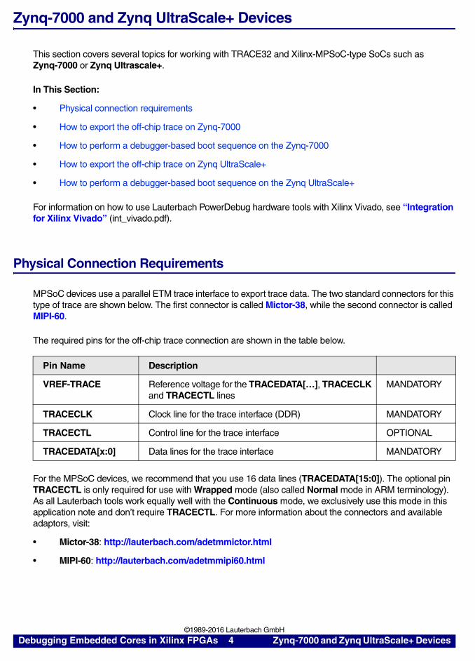
Physical Connection Requirements
MPSoC devices use a parallel ETM trace interface to export trace data. The two standard connectors for this type of trace are shown below. The first connector is called Mictor-38, while the second connector is called MIPI-60.
The required pins for the off-chip trace connection are shown in the table below.
For the MPSoC devices, we recommend that you use 16 data lines (TRACEDATA[15:0]). The optional pin TRACECTL is only required for use with Wrapped mode (also called Normal mode in ARM terminology). As all Lauterbach tools work equally well with the Continuous mode, we exclusively use this mode in this application note and don’t require TRACECTL. For more information about the connectors and available adaptors, visit:
• Mictor-38: http://lauterbach.com/adetmmictor.html
• MIPI-60: http://lauterbach.com/adetmmipi60.html
Pin Name Description
VREF-TRACE Reference voltage for the TRACEDATA[…], TRACECLK and TRACECTL lines
MANDATORY
TRACECLK Clock line for the trace interface (DDR) MANDATORY
TRACECTL Control line for the trace interface OPTIONAL
TRACEDATA[x:0] Data lines for the trace interface MANDATORY
Debugging Embedded Cores in Xilinx FPGAs 4 Zynq-7000 and Zynq UltraScale+ Devices ©1989-2016 Lauterbach GmbH
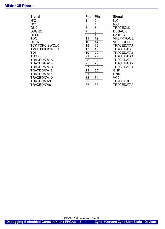
Mictor-38 Pinout
Signal Pin Pin SignalN/C 1 2 N/CN/C 3 4 N/CGND 5 6 TRACECLKDBGRQ 7 8 DBGACKRESET- 9 10 EXTRIGTDO 11 12 VREF-TRACERTCK 13 14 VREF-DEBUGTCK|TCKC|SWCLK 15 16 TRACEDATA7TMS|TMSC|SWDIO 17 18 TRACEDATA6TDI 19 20 TRACEDATA5TRST- 21 22 TRACEDATA4TRACEDATA15 23 24 TRACEDATA3TRACEDATA14 25 26 TRACEDATA2TRACEDATA13 27 28 TRACEDATA1TRACEDATA12 29 30 GNDTRACEDATA11 31 32 GNDTRACEDATA10 33 34 VCCTRACEDATA9 35 36 TRACECTLTRACEDATA8 37 38 TRACEDATA0
Debugging Embedded Cores in Xilinx FPGAs 5 Zynq-7000 and Zynq UltraScale+ Devices ©1989-2016 Lauterbach GmbH

MIPI-60 Pinout
Signal Pin Pin SignalVREF-DEBUG 1 2 TMS|TMSC|SWDIOTCK|TCKC|SWCLK 3 4 TDOTDI 5 6 RESET-RTCK 7 8 TRST- PULLDOWNTRST- 9 10 DBGRQ TRIGINDBGACK TRIGOUT 11 12 VREF-TRACETRACECLK 13 14 GNDGND 15 16 GNDTRACECTL 17 18 TRACEDATA[19]TRACEDATA[0] 19 20 TRACEDATA[20]TRACEDATA[1] 21 22 TRACEDATA[21]TRACEDATA[2] 23 24 TRACEDATA[22]TRACEDATA[3] 25 26 TRACEDATA[23]TRACEDATA[4] 27 28 TRACEDATA[24]TRACEDATA[5] 29 30 TRACEDATA[25]TRACEDATA[6] 31 32 TRACEDATA[26]TRACEDATA[7] 33 34 TRACEDATA[27]TRACEDATA[8] 35 36 TRACEDATA[28]TRACEDATA[9] 37 38 TRACEDATA[29]TRACEDATA[10] 39 40 TRACEDATA[30]TRACEDATA[11] 41 42 TRACEDATA[31]TRACEDATA[12] 43 44 GNDTRACEDATA[13] 45 46 GNDTRACEDATA[14] 47 48 GNDTRACEDATA[15] 49 50 GNDTRACEDATA[16] 51 52 GNDTRACEDATA[17] 53 54 GNDTRACEDATA[18] 55 56 GNDGND 57 58 GNDGND 59 60 GND
Debugging Embedded Cores in Xilinx FPGAs 6 Zynq-7000 and Zynq UltraScale+ Devices ©1989-2016 Lauterbach GmbH

Zynq-7000 Devices
Zynq-7000 devices offer two methods for exporting the off-chip trace interface. The first method uses the Fixed IOs (MIO) pins assigned to the PS part of the SoC. The alternative is to export the trace interface via the FPGA fabric (PL), which allows much more flexible pin assignment than the first method.
This section includes a step-by-step introduction for both methods as well as a step-by-step introduction for performing a debugger-based boot sequence.
Exporting the Zynq-7000 Trace Interface via FixedIO/MIO
1. Create a new Vivado project with an instance of the Zynq processing system.
2. Enter the configuration of the Zynq processing system.
3. Enable the trace pin export via MIO by selecting the desired port size, see [A].
4. Select the external pins that are connected to the trace port, see [B].
A B
Debugging Embedded Cores in Xilinx FPGAs 7 Zynq-7000 and Zynq UltraScale+ Devices ©1989-2016 Lauterbach GmbH
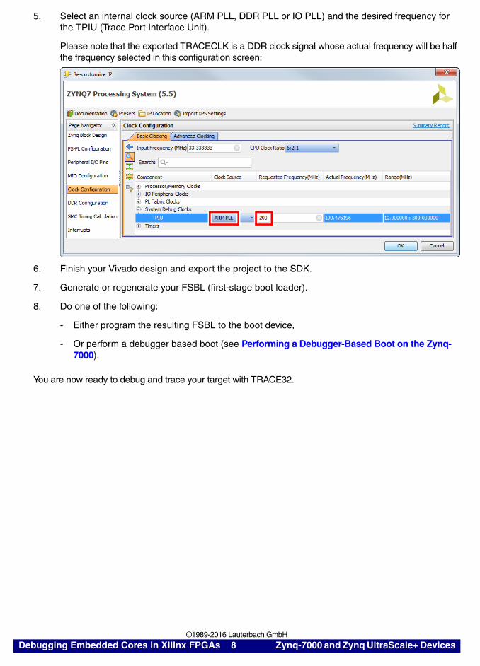
5. Select an internal clock source (ARM PLL, DDR PLL or IO PLL) and the desired frequency for the TPIU (Trace Port Interface Unit).
Please note that the exported TRACECLK is a DDR clock signal whose actual frequency will be half the frequency selected in this configuration screen:
6. Finish your Vivado design and export the project to the SDK.
7. Generate or regenerate your FSBL (first-stage boot loader).
8. Do one of the following:
- Either program the resulting FSBL to the boot device,
- Or perform a debugger based boot (see Performing a Debugger-Based Boot on the Zynq-7000).
You are now ready to debug and trace your target with TRACE32.
Debugging Embedded Cores in Xilinx FPGAs 8 Zynq-7000 and Zynq UltraScale+ Devices ©1989-2016 Lauterbach GmbH

Exporting the Zynq-7000 Trace Interface via FPGA Fabric/PL
1. Create a new Vivado project with an instance of the Zynq processing system.
2. Enter the configuration of the Zynq processing system.
3. Enable the trace pin export via MIO by selecting the desired port size and the pins that will be connected to the trace connector.
4. Activate at least one of the FCLK_CLK<x> clock signals, which will later be used as the TPIU clock. The exported TRACECLK will be half this frequency. Select External as the TPIU clock source.
Debugging Embedded Cores in Xilinx FPGAs 9 Zynq-7000 and Zynq UltraScale+ Devices ©1989-2016 Lauterbach GmbH

5. Connect and export the signals as follows:
To use continuous mode, we do not need the TRACE_CTL signal. The TRACE_CLK_OUT signal will be generated by the HDL wrapper. We rename FCLK_CLK0 to TRACE_CLK_SDR and will use this signal to sample TRACE_DATA.
6. Finish your block design and generate the HDL wrapper.
7. Modify the HDL wrapper to include the pipeline registers and DDR clock generation for routing the PS trace interface to PL pins:
entity zynq_wrapper is port ( oTraceClkDdr: out std_logic; oTraceData: out std_logic_vector(15 downto 0) );end entity;
architecture SDR of zynq_wrapper is signal wTraceClkSdr: std_logic; signal wTraceData: std_logic_vector(15 downto 0);
signal rTraceClkDdr: std_logic; signal rTraceData_q: std_logic_vector(15 downto 0); signal rTraceData_qq: std_logic_vector(15 downto 0);
begin zynq_i: zynq port map ( TRACE_CLK_SDR => wTraceClkSdr, TRACE_DATA => wTraceData );
trace_pipeline: process(wTraceClkSdr) begin if rising_edge(wTraceClkSdr) then rTraceClkDdr <= not rTraceClkDdr; rTraceData_qq <= rTraceData_q; rTraceData_q <= wTraceData; end if; end process;
oTraceData <= rTraceData_qq; oTraceClkDdr <= rTraceClkDdr;end architecture;
Debugging Embedded Cores in Xilinx FPGAs 10 Zynq-7000 and Zynq UltraScale+ Devices ©1989-2016 Lauterbach GmbH

8. Assign the oTraceData[x:0] and oTraceClkDdr to the appropriate FPGA pins matching your board layout. Select the same I/O standard for all pins and the slew rate appropriate for the desired trace port speed.
9. Finish your Vivado design and export the project to the SDK.
10. Generate or regenerate your FSBL (first-stage boot loader).
11. Do one of the following:
- Either program the resulting FSBL to the boot device,
- Or perform a debugger based boot (see “Performing a Debugger-Based Boot on the Zynq-7000”, page 11).
You are now ready to debug and trace your target with TRACE32.
Performing a Debugger-Based Boot on the Zynq-7000
This section focuses on the JTAG-BOOT mode of the Zynq-7000. In contrast to all other boot modes, this mode is only intended for development. The basic idea is that the CPUs will wait in an endless loop after executing the boot ROM, allowing the JTAG probe to perform all further initialization.
To perform a debugger-based boot:
1. Set the boot mode to JTAG-BOOT using the MIO lines.
2. Reset the SoC, for example by asserting the RESET line. Not all boards have a RESET line connected to the SoC, thus a power cycle or similar might be required.
3. Execute the boot ROM.
4. Load the FSBL boot code using the debugger.
5. Execute the FSBL boot code.
6. Optionally load the FPGA fabric using the debugger.
7. You are now ready to load the next stage boot loader, OS, … and to use the optional off-chip trace.
Example files following the above sequence are included in the TRACE32 installation directory under ~~/demo/arm/hardware/zynq-7000
Debugging Embedded Cores in Xilinx FPGAs 11 Zynq-7000 and Zynq UltraScale+ Devices ©1989-2016 Lauterbach GmbH

UltraScale+ Devices
Zynq UltraScale devices offer two methods for exporting the off-chip trace interface. The first method uses the Fixed IOs (MIO) pins assigned to the PS part of the SoC. The alternative is to export the trace interface via the FPGA fabric (PL), which allows much more flexible pin assignment than the first method.
This section includes a step-by-step introduction for both methods as well as a step-by-step introduction for performing a debugger-based boot sequence.
Exporting the UltraScale+ Trace Interface via FixedIO/MIO
1. Create a new Vivado project with an instance of the Zynq processing system.
2. Enter the configuration of the Zynq processing system.
3. Enable the trace pin export via MIO by selecting the desired port size and the pins that will be connected to the trace connector.
Debugging Embedded Cores in Xilinx FPGAs 12 Zynq-7000 and Zynq UltraScale+ Devices ©1989-2016 Lauterbach GmbH

4. Select an internal clock source (IOPLL, DPLL or APLL) and the desired frequency for DBG Trace. Please note that the exported TRACECLK is a DDR clock signal whose actual frequency will be half the frequency selected in this configuration screen.
5. Finish your Vivado design and export the project to the SDK.
6. Generate or regenerate your FSBL (first-stage boot loader).
7. Do one of the following:
- Either program the resulting FSBL to the boot device,
- Or perform a debugger based boot (see “Performing a Debugger-Based Boot on the Zynq UltraScale+”, page 16).
You are now ready to debug and trace your target with TRACE32.
Debugging Embedded Cores in Xilinx FPGAs 13 Zynq-7000 and Zynq UltraScale+ Devices ©1989-2016 Lauterbach GmbH

Exporting the Zynq UltraScale+ Trace Interface via FPGA Fabric/PL
1. Create a new Vivado project with an instance of the Zynq processing system.
2. Enter the configuration of the Zynq processing system.
3. Enable the trace pin export via EMIO by selecting the desired port size.
4. Activate at least one of the PL Fabric Clocks (for example PL0), which will later be used as the TPIU clock. The exported TRACECLK will be half this frequency. Select FMIO traceclk as the TPIU clock source.
Debugging Embedded Cores in Xilinx FPGAs 14 Zynq-7000 and Zynq UltraScale+ Devices ©1989-2016 Lauterbach GmbH

5. Connect and export the signals as follows:
To use continuous mode, we do not need the TRACE_CTL signal. The trace_clk_out signal will be generated by the HDL wrapper. We rename pl_clk0 to TRACE_CLK_SDR and will use this signal to sample TRACE_DATA. As of Vivado 2016.1, the ps_pl_tracedata signal does not respect the port size setting and is always 32 bits wide.
6. Finish your block design and generate the HDL wrapper.
7. Modify the HDL wrapper to include the pipeline registers and DDR clock generation for routing the PS trace interface to PL pins:
entity zynq_wrapper is port ( oTraceClkDdr: out std_logic; oTraceData: out std_logic_vector(15 downto 0) );end entity;
architecture SDR of zynq_wrapper is signal wTraceClkSdr: std_logic; signal wTraceData: std_logic_vector(31 downto 0);
signal rTraceClkDdr: std_logic; signal rTraceData_q: std_logic_vector(15 downto 0); signal rTraceData_qq: std_logic_vector(15 downto 0);
begin zynq_i: zynq port map ( TRACE_CLK_SDR => wTraceClkSdr, TRACE_DATA => wTraceData );
trace_pipeline: process(wTraceClkSdr) begin if rising_edge(wTraceClkSdr) then rTraceClkDdr <= not rTraceClkDdr; rTraceData_qq <= rTraceData_q; rTraceData_q <= wTraceData(15 downto 0); end if; end process;
oTraceData <= rTraceData_qq; oTraceClkDdr <= rTraceClkDdr;end architecture;
Debugging Embedded Cores in Xilinx FPGAs 15 Zynq-7000 and Zynq UltraScale+ Devices ©1989-2016 Lauterbach GmbH

8. Assign the oTraceData[x:0] and oTraceClkDdr to the appropriate FPGA pins matching your board layout. Select the same I/O standard for all pins and the slew rate appropriate for the desired trace port speed.
9. Finish your Vivado design and export the project to the SDK.
10. Generate or regenerate your FSBL (first-stage boot loader).
11. Do one of the following:
- Either program the resulting FSBL to the boot device,
- Or perform a debugger based boot (see “Performing a Debugger-Based Boot on the Zynq UltraScale+”, page 16).
You are now ready to debug and trace your target with TRACE32.
Performing a Debugger-Based Boot on the Zynq UltraScale+
This section focuses on the JTAG-BOOT mode of the ZynqUltraScale+. In contrast to all other boot modes, this mode is only intended for development. The basic idea is that the CPUs will wait in an endless loop after executing the boot ROM, allowing the JTAG probe to perform all further initialization.
To perform a debugger-based boot:
1. Set the boot mode to JTAG-BOOT using the MIO lines.
2. Reset the SoC, for example by asserting the RESET line. Not all boards have a RESET line connected to the SoC, thus a power cycle or similar might be required.
3. Execute the boot ROM.
4. Load the FSBL boot code using the debugger.
5. Execute the FSBL boot code.
6. Optionally load the FPGA fabric using the debugger.
7. You are now ready to load the next stage boot loader, OS, … and to use the optional off-chip trace.
Example files following the above sequence are included in the TRACE32 installation directory under ~~/demo/arm64/hardware/zynq_ultrascale.
Debugging Embedded Cores in Xilinx FPGAs 16 Zynq-7000 and Zynq UltraScale+ Devices ©1989-2016 Lauterbach GmbH
Virtex Devices Containing PPC400/PPC440 Cores
This section deals with the older series of Virtex devices that contain one or more PPC400/PPC440 cores.
In This Section:
• Software, hardware and physical connection requirements
• Setup for debug and trace of multi-core systems
• Frequently asked questions
For information on how to use Lauterbach PowerDebug hardware tools with Xilinx ISE, see “Using TRACE32 as Backend for Xilinx ISE” (int_ise.pdf).
TRACE32 Software Requirements
When using the FPGA’s configuration JTAG pins also for PPC debugging, the following versions of the TRACE32 software are required:
PPC405 If this application note advises to use SYStem.CPU VirtexPPC, a TRACE32 version from May 2006 or later is required. If your software does not offer this setting, you need to get an update.
Any attempt to use SYStem.CPU PPC405F or SYStem.CPU PPC405D instead of SYStem.CPU VirtexPPC will fail.
PPC440 To debug a PPC440 core in a Virtex5FXT (using SYStem.CPU Virtex5PPC, SYStem.CPU Virtex5PPC1st, or SYStem.CPU Virtex5PPC2nd), a software version later than March 2008 is required.
Debugging Embedded Cores in Xilinx FPGAs 17 Virtex Devices Containing PPC400/PPC440 ©1989-2016 Lauterbach GmbH

Supported TRACE32 JTAG Cables
When connecting to Xilinx targets, be sure to use a recent version of the debug cable (see picture below). With the old version of the debug cable target connection will fail or be unreliable.
Physical Connection of the TRACE32 Debugger
For CONNECTING the TRACE32-ICD to the target, there are two main options that are reflected in the FPGA design:
1. Connecting the PPC core’s JTAG signals to FPGA’s user I/O pins. Many boards provide a 16 pin connector (“CPU DEBUG”) for this purpose.
2. Using the target board’s 14-pin JTAG connector (“Configuration JTAG”) and include the Xilinx JTAGPPC controller (an IP block used by Base System Builder) in the design.
Using user I/O is preferable, if the boot code of the PPC shall be debugged because it provides the additional HALT signal which allows the debugger to stop the PPC after a reset at the reset vector without executing any code.This signal is not available on the 14 pin connector and should be pulled high. In this case, after a reset the PPC core will execute some code before being stopped by the debugger.
The advantage of using the 14 pin connector is that it serves to reconfigure the FPGA (via the command JTAG.LOADBIT) and for debugging.
For hints on correctly implementing the aforementioned connections in an FPGA design, see section “Design Considerations for Debugging and Tracing Embedded Cores”.
JTAG Connection via 16-pin PPC Connector
When JTAG is connected via FPGA user I/O pins to a standard PPC 16-pin PPC JTAG connector, no adaptation is required.
Debug Cable
Old VersionNot to use with Xilinx FPGAs
New Version
Debugging Embedded Cores in Xilinx FPGAs 18 Virtex Devices Containing PPC400/PPC440 ©1989-2016 Lauterbach GmbH
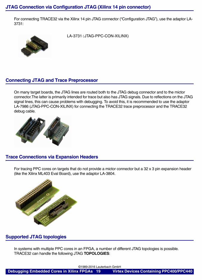
JTAG Connection via Configuration JTAG (Xilinx 14 pin connector)
For connecting TRACE32 via the Xilinx 14 pin JTAG connector (“Configuration JTAG”), use the adaptor LA-3731:
Connecting JTAG and Trace Preprocessor
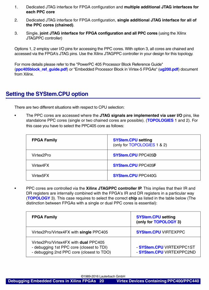
On many target boards, the JTAG lines are routed both to the JTAG debug connector and to the mictor connector.The latter is primarily intended for trace but also has JTAG signals. Due to reflections on the JTAG signal lines, this can cause problems with debugging. To avoid this, it is recommended to use the adaptor LA-7986 (JTAG-PPC-CON-XILINX) for connecting the TRACE32 trace preprocessor and the TRACE32 debug cable.
Trace Connections via Expansion Headers
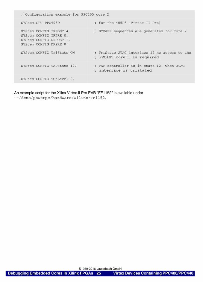
For tracing PPC cores on targets that do not provide a mictor connector but a 32 x 3 pin expansion header (like the Xilinx ML403 Eval Board), use the adaptor LA-3804.
Supported JTAG topologies
In systems with multiple PPC cores in an FPGA, a number of different JTAG topologies is possible. TRACE32 can handle the following JTAG TOPOLOGIES:
LA-3731(JTAG-PPC-CON-XILINX)
Debugging Embedded Cores in Xilinx FPGAs 19 Virtex Devices Containing PPC400/PPC440 ©1989-2016 Lauterbach GmbH
1. Dedicated JTAG interface for FPGA configuration and multiple additional JTAG interfaces for each PPC core
2. Dedicated JTAG interface for FPGA configuration, single additional JTAG interface for all of the PPC cores (chained).
3. Single, joint JTAG interface for FPGA configuration and all PPC cores (using the Xilinx JTAGPPC controller)
Options 1, 2 employ user I/O pins for accessing the PPC cores. With option 3, all cores are chained and accessed via the FPGA’s JTAG pins. Use the Xilinx JTAGPPC controller in your design for this topology.
For more details please refer to the "PowerPC 405 Processor Block Reference Guide" (ppc405block_ref_guide.pdf) or “Embedded Processor Block in Virtex-5 FPGAs“ (ug200.pdf) document from Xilinx.
Setting the SYStem.CPU option
There are two different situations with respect to CPU selection:
• The PPC cores are accessed where the JTAG signals are implemented via user I/O pins, like standalone PPC cores (single or two chained cores are possible). (TOPOLOGIES 1 and 2). For this case you have to select the PPC405 core as follows:
• PPC cores are controlled via the Xilinx JTAGPPC controller IP. This implies that their IR and DR registers are internally combined with the FPGA’s IR and DR registers in a particular way (TOPOLOGY 3). This case requires to select the correct chip as listed in the table below (The distinction between FPGAs with a single or dual PPC cores is essential):
FPGA Family SYStem.CPU setting (only for TOPOLOGIES 1 & 2)
Virtex2Pro SYStem.CPU PPC405D
Virtex4FX SYStem.CPU PPC405F
Virtex5FX SYStem.CPU PPC440G
FPGA Family SYStem.CPU setting (only for TOPOLOGY 3)
Virtex2Pro/Virtex4FX with single PPC405 SYStem.CPU VIRTEXPPC
Virtex2Pro/Virtex4FX with dual PPC405- debugging 1st PPC core (closest to TDI)- debugging 2nd PPC core (closest to TDO)
- SYStem.CPU VIRTEXPPC1ST- SYStem.CPU VIRTEXPPC2ND
Debugging Embedded Cores in Xilinx FPGAs 20 Virtex Devices Containing PPC400/PPC440 ©1989-2016 Lauterbach GmbH

The CPU settings "VirtexPPC", "VirtexPPC1st", "VirtexPPC2nd" are available in SW from May 2006 or later. If your SW does not offer this setting, you need to get an update. Any attempt to use PPC405F or PPC405D (for the case of TOPOLOGY 3) instead will fail and is a waste of time.
Multicore Settings for Xilinx FPGAs
In addition to making the correct SYStem.CPU selection, it is required to make multicore settings so that the debugger accesses the correct device in the JTAG chain.
The settings are made in the SYStem.CONFIG window:
The actual calculation of the multicore settings is described in the following sections. It requires the knowledge of the size of the JTAG instruction register (IR) of the FPGA. The following table lists information useful for this purpose for all Xilinx FPGAs with embedded PPC400/PPC440 cores.
Xilinx Virtex2Pro devices:
Virtex5FX with single PPC440 SYStem.CPU VIRTEX5PPC
Virtex5FX with dual PPC440- debugging 1st PPC core (closest to TDI)- debugging 2nd PPC core (closest to TDO)
- SYStem.CPU VIRTEX5PPC1ST- SYStem.CPU VIRTEX5PPC2ND
FPGA Number of PPC405 cores
Number of Instruction Register Bits PPC405
Number of Instruction Register Bits (IR-length)
SYStem.CPU (when implemented with JTAGPPC primitive)
XC2VP2 0 0 6 -
XC2VP4 1 4 10 VIRTEXPPC
XC2VP7 1 4 10 VIRTEXPPC
XC2VP20 2 4+4 14 VIRTEXPPC1ST orVIRTEXPPC2ND
XC2VPX20 2 4+4 14 VIRTEXPPC1ST orVIRTEXPPC2ND
XC2VP30 2 4+4 14 VIRTEXPPC1ST orVIRTEXPPC2ND
Debugging Embedded Cores in Xilinx FPGAs 21 Virtex Devices Containing PPC400/PPC440 ©1989-2016 Lauterbach GmbH

Xilinx Virtex4FX devices
Xilinx Virtex5FXT devices:
XC2VP40 2 4+4 14 VIRTEXPPC1ST orVIRTEXPPC2ND
XC2VP50 2 4+4 14 VIRTEXPPC1ST orVIRTEXPPC2ND
XC2VP70 2 4+4 14 VIRTEXPPC1ST orVIRTEXPPC2ND
XC2VPX70 2 4+4 14 VIRTEXPPC1ST orVIRTEXPPC2ND
XC2VP100 2 4+4 14 VIRTEXPPC1ST orVIRTEXPPC2ND
FPGA Number of PPC405 cores
Number of Instruction Register Bits PPC405
Number of Instruction Register Bits (IR-length)
SYStem.CPU (when implemented with JTAGPPC primitive)
XC4VFX12 1 4 10 VIRTEXPPC
XC4VFX20 1 4 10 VIRTEXPPC
XC4VFX40 1 4 10 VIRTEXPPC
XC4VFX60 1 4 10 VIRTEXPPC
XC4VFX100 2 4+4 14 VIRTEXPPC1ST orVIRTEXPPC2ND
XC4VFX140 2 4+4 14 VIRTEXPPC1ST orVIRTEXPPC2ND
FPGA Number of PPC440 cores
Number of Instruction Register Bits PPC440
Number of Instruction Register Bit FPGA
SYStem.CPU (when implemented with JTAGPPC primitive)
XC5VFX30T 1 4 10 VIRTEX5PPC
XC5VFX70T 1 4 10 VIRTEX5PPC
XC5VFX100T 2 4+4 14 VIRTEX5PPC1ST orVIRTEX5PPC2ND
XC5VFX130T 2 4+4 14 VIRTEX5PPC1ST orVIRTEX5PPC2ND
XC5VFX200T 2 4+4 14 VIRTEX5PPC1ST orVIRTEX5PPC2ND
Debugging Embedded Cores in Xilinx FPGAs 22 Virtex Devices Containing PPC400/PPC440 ©1989-2016 Lauterbach GmbH

1st Topology: Separate JTAG Interfaces for FPGA and each PPC Core
The PPC405 JTAG core signals have to be routed to arbitrary USER-GPIO pins of the FPGA.
As each core has a separate JTAG chain, the multicore settings can remain at the default settings (IRPRE=IRPOST=DRPRE=DRPOST=0). NO multicore settings are necessary. Just select the correct CPU (Core) build in the FPGA (page 17 in ppc405block_ref_guide.pdf):
SYStem.CPU PPC405DSYStem.BdmClock 1.MHz
; for the 405D5 (Virtex-II Pro) use a low JTAG; frequency to start debugging
SYStem.CPU PPC405FSYStem.BdmClock 1.MHz
; for the 405F6 (Virtex-4) use a low JTAG; frequency to start debugging
Virtex-II Pro / Virtex-4
PPC405/440 core
TDI
TMS
TCK
TDI
TMS
TCK
TDI
TMS
TCK
TDOTDO
TDOConfigurationJTAG
Debugging Embedded Cores in Xilinx FPGAs 23 Virtex Devices Containing PPC400/PPC440 ©1989-2016 Lauterbach GmbH

2nd Topology: Separate FPGA JTAG/ joint PPC JTAG for all PPC Cores
This 2nd topology includes a separate JTAG interface for the FPGA and a joint JTAG interface for all PPC Cores.
This script assumes that each core is debugged by a separate TRACE32 debugger. Here the JTAG interface has to be tristated, when the debugger does not communicate via JTAG with its related core.
; Configuration example for PPC405 core 1
SYStem.CPU PPC405D ; for the 405D5 (Virtex-II Pro)
SYStem.CONFIG IRPOST 0.SYStem.CONFIG IRPRE 4.SYStem.CONFIG DRPOST 0.SYStem.CONFIG DRPRE 1.
; BYPASS sequences are generated for the other; PPC core
SYStem.CONFIG TriState ON ; TriState JTAG interface if no access to the; PPC405 core 1 is required
SYStem.CONFIG TAPState 12. ; TAP controller is in state 12. when JTAG; interface is tristated
SYStem.CONFIG TCKLevel 0.
Virtex-II Pro / Virtex-4
PPC405 core 1
TDI
TMS
TCK
TDI
TMS
TCK
TDI
TMS
TCK
TDO
PPC405 core 2
TDI
TMS
TCK
TDO
TDO
TDI
TMS
TDO
Number ofinstruction register bits
4
Number ofinstruction register bits
4
The number of data register bits is always 1 in BYPASS mode
ConfigurationJTAG
Debugging Embedded Cores in Xilinx FPGAs 24 Virtex Devices Containing PPC400/PPC440 ©1989-2016 Lauterbach GmbH
An example script for the Xilinx Virtex-II Pro EVB "FF1152" is available under ~~/demo/powerpc/hardware/Xilinx/FF1152.
; Configuration example for PPC405 core 2
SYStem.CPU PPC405D ; for the 405D5 (Virtex-II Pro)
SYStem.CONFIG IRPOST 4.SYStem.CONFIG IRPRE 0.SYStem.CONFIG DRPOST 1.SYStem.CONFIG DRPRE 0.
; BYPASS sequences are generated for core 2
SYStem.CONFIG TriState ON ; TriState JTAG interface if no access to the; PPC405 core 1 is required
SYStem.CONFIG TAPState 12. ; TAP controller is in state 12. when JTAG; interface is tristated
SYStem.CONFIG TCKLevel 0.
Debugging Embedded Cores in Xilinx FPGAs 25 Virtex Devices Containing PPC400/PPC440 ©1989-2016 Lauterbach GmbH

3rd Topology: Joint JTAG Interface for the FPGA and all PPC400/PPC440 Cores
For generating this topology you have to use the Xilinx JTAGPPC controller in your FPGA design.
The following picture shows a Xilinx XC2VP7, containing a single PPC405 core.
In this case take care of the special JTAG characteristic of the JTAGPPC controller. The PPC400/PPC440 core and the FPGA will not be handled as independent JTAG devices: even though they have separate (concatenated) IR registers, they share a single DR register.
NOTE: This topology requires the use of the CPU setting “VirtexPPC” which is available in the SW from May 2006 or later. If your SW does not offer this setting, you need to get an update. Any attempt to use PPC405F or PPC405D instead will fail and is a waste of time.
; Configuration
SYStem.CPU VIRTEXPPC ; for a Virtex2Pro/Virtex4FX with a single; PPC405 core
SYStem.CONFIG IRPOST 0.SYStem.CONFIG IRPRE 0.SYStem.CONFIG DRPOST 0.SYStem.CONFIG DRPRE 0.
; BYPASS sequences are generated for the FPGA
SYStem.CONFIG TriState OFF ; no tristating of JTAG interface required
PPC405 core
TDI
TMS
TCK
TDI
TMS
TCK
FPGATDOTDO
Virtex-II Pro / Virtex-4
ConfigurationJTAG
XC2VP7: (9:0)
PPC405_IR(3:0) FPGA_IR(5:0)
IR-Path: (Number of instruction register bits == 10)
TDI TDO
DR-Path: (Number of data register bits in BYPASS mode == 1)
BYPASS length = 1
Debugging Embedded Cores in Xilinx FPGAs 26 Virtex Devices Containing PPC400/PPC440 ©1989-2016 Lauterbach GmbH

The following example shows the multi-core settings for the ML403 Virtex-4 EVB, assuming an FPGA design with the JTAGPPC controller. The debugger has to be connected to the target board’s 14-pin JTAG connector (using a custom adaptor):
For testing the setup just power up the ML403: Provided you have the original CF card inserted, the board will boot a small FPGA design that controls the LCD screen and push buttons: please check that you can switch between different menu entries before proceeding. Do not start any menu entry at this point (which would be done by the middle button). Instead attach to the PPC400/PPC440 core used by this menu control program and try to debug it: when you stop the core the board will not react to push buttons any more. When you resume the program it will continue and you can select one of the sample designs.
; Configuration
SYStem.CPU VIRTEXPPC ; for a Virtex4FX (XC4VFX12) with a single; PPC405 core
SYStem.CONFIG IRPOST 24.SYStem.CONFIG IRPRE 8.SYStem.CONFIG DRPOST 2.SYStem.CONFIG DRPRE 1.
; SYSACE+PlatFlash; CPLD; SYSACE+PlatFlash; CPLD; only one DR for PPC and FPGA!
SYStem.CONFIG TriState OFF ; no tristating of JTAG interface; required
PPC405 core
TDI
TMS
TCK
TDI
TMS
TCK
FPGA
TMS
TCK
TMS
TDO
TDI
TMS
TCK
TDOTDI
TMS
TCK
TDO
SYSACE PlatFlash
TDI
TMS
TCK
TDO
CPLD
XC4VFX12
TDI
Number of IR(instruction reg.) and BYPASS-DR(data reg.) bits
SYSACE(7:0) PlatFlash(15:0)XC4VFX12
CPLD(7:0)PPC_CORE(3:0) FPGA(5:0)
IR = 8 IR = 16 IR = 10 IR = 8TDO
DR = 1 DR = 1 DR = 1 DR = 1
Debugging Embedded Cores in Xilinx FPGAs 27 Virtex Devices Containing PPC400/PPC440 ©1989-2016 Lauterbach GmbH

Design Considerations for Debugging and Tracing
This section lists some considerations for creating FPGA designs to debug and trace embedded PPC405 and PPC440 cores.
Debugging Embedded PPC405 Cores
An FPGA design for debugging an embedded PPC405 core needs to consider that these have a high-active HALT signal rather than a HALT- signal.
When using a Xilinx “wizard” (like the base system builder) this is taken into account automatically by inserting an inverter. If you manually create JTAG connections for your design, consider the actual polarity of the signal. If HALT/HALT- are pulled to the wrong level, the PPC cores will remain halted i.e. execute no code.
The TRST- should also be connected to the debugger because some chips need to have it activated once at the beginning of the debug session for resetting the JTAG controller. By using the Xilinx JTAGPPC controller in your design, correct reset of the JTAG controller is ensured. In this case the TRST- signal does not need to be connected to the debugger and should be pulled high (internally in the design).
Tracing Embedded PPC405 Cores
Tracing embedded PPC405 cores in Xilinx Virtex devices requires a small adaptation to the design. The reason is that most PPC405 cores use the rising edge of the trace clock to output data whereas the PPC405 in Xilinx Virtex devices uses the falling edge. This can be compensated inverting the trace clock inside the design. This is done by changing the system.mhs file by adding an inverter and connecting its output to the pin used for the trace clock:
Without this, the trace will sample the clock at the wrong edge and detect lots of flow errors or show no sensible data at all.
When designing a board with trace port for PPC405 it is suggested to use a mictor connector for good signal quality. For the pinout see "Adapter PPC405/Mictor Connector 38 pin" on http://lauterbach.com/adppc400.html.
PORT fpga_0_ppc405_0_C405TRCCYCLE_pin = trccycle_inverted, DIR = O
BEGIN util_vector_logic PARAMETER INSTANCE = trccycle_INV PARAMETER HW_VER = 1.00.a PARAMETER C_OPERATION = not PARAMETER C_SIZE = 1 PORT Res = trccycle_inverted PORT Op1 = fpga_0_ppc405_0_C405TRCCYCLE
END
Debugging Embedded Cores in Xilinx FPGAs 28 Virtex Devices Containing PPC400/PPC440 ©1989-2016 Lauterbach GmbH

Debugging Embedded PPC440 Cores
When creating an FPGA design including a PPC440 core, ensure the correct polarity of the HALT line. The PPC440 IP in Xilinx FPGAs use positive polarity while the TRACE32 debugger (in line with the standard) uses negative polarity.
If the polarity of the HALT line is incorrect, the PPC440 will not execute code after the “GO” command, even though single stepping the code does work.
The easiest way to avoid problems is to connect the HALT line of the debug connector as follows:
Tracing Embedded PPC440 Cores using TRACE32
The connection between the PowerPC 440 trace interface signals and the TRACE32 mictor connector has to be made as follows:
For the pinout see "Trace and Debug Connector" on http://lauterbach.com/adicd440.html.
Frequently Asked Questions
Virtex2Pro, Virtex4FX, Virtex5FXT: TRACE32 does not display ISOCM memories
On Virtex2Pro the ISOCM (instruction side on chip memories) memories can only be initialized through bitstream download. As the only possible access type is instruction fetch, there is no way for the debugger to read ISOCM memory. On Virtex2Pro the debugger will always display 0x0 for the address range mapped to ISOCM memory.
On Virtex4FX, Virtex5FX the ISOCM memory can be read using a special access mechanism. Configure the first address of the ISOCM using the system option SYStem.Option ISOCM <baseaddr>. The default value is 0xFFFF.FFFF, indicating that the system under debug does not have ISOCM memory.
BEGIN ppc440_virtex5 PARAMETER INSTANCE = ppc440_0 [...] PORT DBGC440DEBUGHALTNEG = fpga_0_ppc440_0_DBGC440DEBUGHALTNEG_pin [...]END
PowerPC 440 Trace interface signal TRACE32 mictor
C440TRCCYCLE C440TRCEXECUTIONSTATUS[0:4] : C440TRCTRACESTATUS[0:6] C440TRCBRANCHSTATUS[0:2]
TRACECLKES0-ES4TS0-TS6BS0-BS2
Debugging Embedded Cores in Xilinx FPGAs 29 Virtex Devices Containing PPC400/PPC440 ©1989-2016 Lauterbach GmbH

For a design with ISOCM memory from 0xFFFF.8000--0xFFFF.FFFF you should therefore use:
Flow errors tracing PPC cores on Xilinx ML310 eval board
In some revisions of the Xilinx ML310 board there are problems with flow errors when tracing the program flow. The reason is that the GND pins (planes) in the middle of the mictor connector used for tracing is not connected to GND signal on the board. This floating connection will cause lots flow errors or unusable trace. The problem can be fixed by manually soldering the required connection.
SYStem.Option ISOCM 0xFFFF8000
NOTE: This feature is available in SW from 2006-10-20 or later.
Debugging Embedded Cores in Xilinx FPGAs 30 Virtex Devices Containing PPC400/PPC440 ©1989-2016 Lauterbach GmbH
Related Documents


