DE10-Nano User Manual 1 www.terasic.com December 22, 2016

Welcome message from author
This document is posted to help you gain knowledge. Please leave a comment to let me know what you think about it! Share it to your friends and learn new things together.
Transcript
DE10-Nano
User Manual
1 www.terasic.com
December 22, 2016
DE10-Nano
User Manual
1 www.terasic.com
December 22, 2016
Chapter 1 DE10-Nano Development Kit 3
1.1 Package Contents 3 1.2 DE10-Nano System CD 4 1.3 Getting Help 4
Chapter 2 Introduction of the DE10-Nano Board 5
2.1 Layout and Components 5 2.2 Block Diagram of the DE10-Nano Board 8
Chapter 3 Using the DE10-Nano Board 11
3.1 Settings of FPGA Configuration Mode 11 3.2 Configuration of Cyclone V SoC FPGA on DE10-Nano 13 3.3 Board Status Elements 20 3.4 Board Reset Elements 21 3.5 Clock Circuitry 22 3.6 Peripherals Connected to the FPGA 24
3.6.1 User Push-buttons, Switches and LEDs 24 3.6.2 2x20 GPIO Expansion Headers 27 3.6.3 Arduino Uno R3 Expansion Header 30 3.6.4 A/D Converter and Analog Input 32 3.6.5 HDMI TX Interface 34
3.7 Peripherals Connected to Hard Processor System (HPS) 36 3.7.1 User Push-buttons and LEDs 36 3.7.2 Gigabit Ethernet 36 3.7.3 UART 38 3.7.4 DDR3 Memory 39 3.7.5 Micro SD Card Socket 41 3.7.6 USB 2.0 OTG PHY 42 3.7.7 G-sensor 43 3.7.8 LTC Connector 44
Chapter 4 DE10-Nano System Builder 45
4.1 Introduction 45 4.2 Design Flow 46 4.3 Using DE10-Nano System Builder 47
DE10-Nano
User Manual
2 www.terasic.com
December 22, 2016
Chapter 5 Examples For FPGA 53
5.1 DE10-Nano Factory Configuration 53 5.2 ADC Reading 54 5.3 HDMI TX 57 5.4 DDR3_VIP 61
Chapter 6 Examples for HPS SoC 67
6.1 Hello Program 67 6.2 Users LED and KEY 70 6.3 I2C Interfaced G-sensor 77
Chapter 7 Examples for using both HPS SoC and FGPA 80
7.1 Required Background 80 7.2 System Requirements 81 7.3 AXI bridges in Intel SoC FPGA 81 7.4 GHRD Project 83 7.5 Compile and Programming 84 7.6 Develop the C Code 85
Chapter 8 Programming the EPCS Device 91
8.1 Before Programming Begins 91 8.2 Convert .SOF File to .JIC File 92 8.3 Write JIC File into the EPCS Device 97 8.4 Erase the EPCS Device 99 8.5 EPCS Programming via nios-2-flash-programmer 100 8.6 Nios II Boot from EPCS Device in Quartus II v14.1 100
Chapter 9 Appendix A 101
9.1 Revision History 101
DE10-Nano
User Manual
3 www.terasic.com
December 22, 2016
Chapter 1 DE10-Nano
Development Kit
he DE10-Nano Development Kit presents a robust hardware design platform built
around the Intel System-on-Chip (SoC) FPGA, which combines the latest dual-core
Cortex-A9 embedded cores with industry-leading programmable logic for ultimate
design flexibility. Users can now leverage the power of tremendous re-configurability paired
with a high-performance, low-power processor system. Intel’s SoC integrates an
ARM-based hard processor system (HPS) consisting of processor, peripherals and
memory interfaces tied seamlessly with the FPGA fabric using a high-bandwidth
interconnect backbone. The DE10-Nano development board is equipped with high-speed
DDR3 memory, analog to digital capabilities, Ethernet networking, and much more that
promise many exciting applications.
The DE10-Nano Development Kit contains all the tools needed to use the board in
conjunction with a computer that runs the Microsoft Windows XP or later.
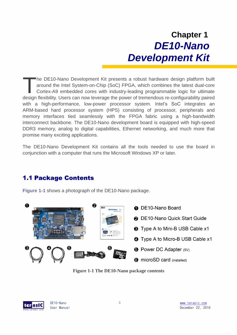
1.1 PPaacckkaaggee CCoonntteennttss
Figure 1-1 shows a photograph of the DE10-Nano package.
Figure 1-1 The DE10-Nano package contents
T
DE10-Nano
User Manual
4 www.terasic.com
December 22, 2016
The DE10-Nano package includes:
The DE10-Nano development board
DE10-Nano Quick Start Guide
USB cable Type A to Mini-B for FPGA programming or UART control
USB cable Type A to Micro-B for USB OTG connect to PC
5V/2A DC power adapter
microSD Card (Installed)
1.2 DDEE1100--NNaannoo SSyysstteemm CCDD
The DE10-Nano System CD contains all the documents and supporting materials
associated with DE10-Nano, including the user manual, system builder, reference designs,
and device datasheets. Users can download this system CD from the link:
http://de10-nano.terasic.com/cd.
1.3 GGeettttiinngg HHeellpp
Here are the addresses where you can get help if you encounter any problems:
Intel Corporation
101 Innovation Drive San Jose, California, 95134 USA
Email: [email protected]
Terasic Technologies
9F., No.176, Sec.2, Gongdao 5th Rd, East Dist, Hsinchu City, 30070. Taiwan
Email: [email protected]
Tel.: +886-3-575-0880
Website: DE10-Nano.terasic.com
DE10-Nano
User Manual
5 www.terasic.com
December 22, 2016
Chapter 2 Introduction of the DE10-Nano Board
his chapter provides an introduction to the features and design characteristics of the
board.
2.1 LLaayyoouutt aanndd CCoommppoonneennttss
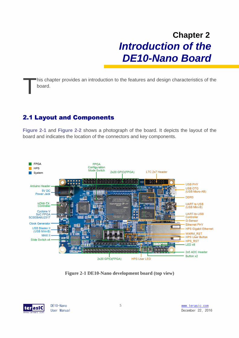
Figure 2-1 and Figure 2-2 shows a photograph of the board. It depicts the layout of the
board and indicates the location of the connectors and key components.
Figure 2-1 DE10-Nano development board (top view)
T
DE10-Nano
User Manual
6 www.terasic.com
December 22, 2016
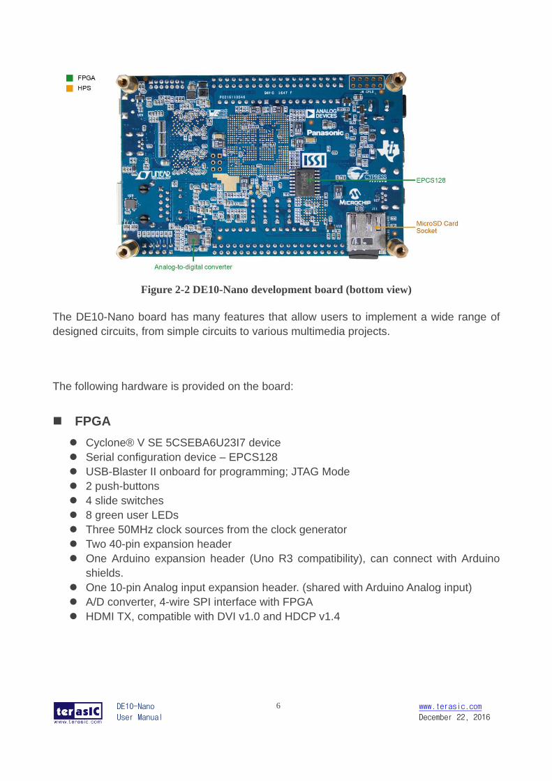
Figure 2-2 DE10-Nano development board (bottom view)
The DE10-Nano board has many features that allow users to implement a wide range of
designed circuits, from simple circuits to various multimedia projects.
The following hardware is provided on the board:
FPGA
Cyclone® V SE 5CSEBA6U23I7 device
Serial configuration device – EPCS128
USB-Blaster II onboard for programming; JTAG Mode
2 push-buttons
4 slide switches
8 green user LEDs
Three 50MHz clock sources from the clock generator
Two 40-pin expansion header
One Arduino expansion header (Uno R3 compatibility), can connect with Arduino
shields.
One 10-pin Analog input expansion header. (shared with Arduino Analog input)
A/D converter, 4-wire SPI interface with FPGA
HDMI TX, compatible with DVI v1.0 and HDCP v1.4
DE10-Nano
User Manual
7 www.terasic.com
December 22, 2016
HPS (Hard Processor System)
925MHz Dual-core ARM Cortex-A9 processor
1GB DDR3 SDRAM (32-bit data bus)
1 Gigabit Ethernet PHY with RJ45 connector
port USB OTG, USB Micro-AB connector
Micro SD card socket
Accelerometer (I2C interface + interrupt)
UART to USB, USB Mini-B connector
Warm reset button and cold reset button
One user button and one user LED
LTC 2x7 expansion header
DE10-Nano
User Manual
8 www.terasic.com
December 22, 2016
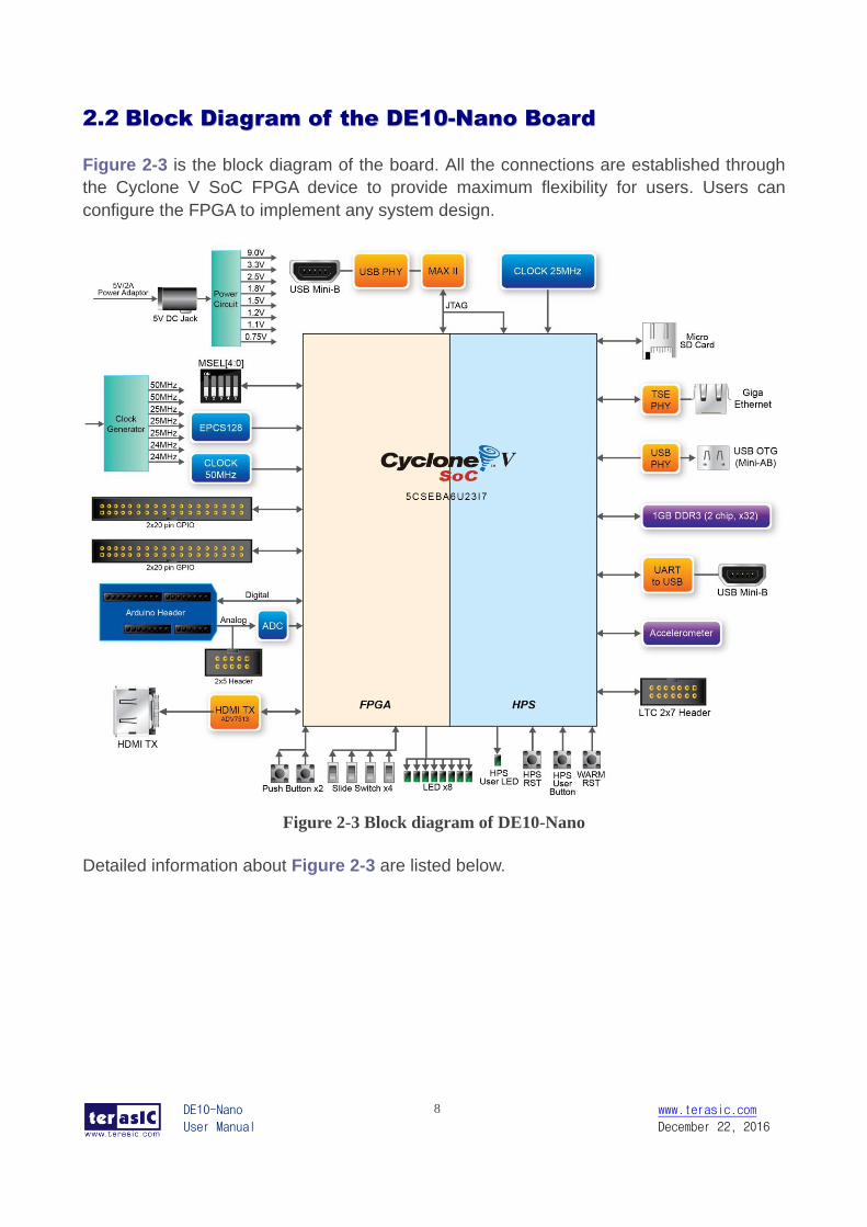
2.2 BBlloocckk DDiiaaggrraamm ooff tthhee DDEE1100--NNaannoo BBooaarrdd
Figure 2-3 is the block diagram of the board. All the connections are established through
the Cyclone V SoC FPGA device to provide maximum flexibility for users. Users can
configure the FPGA to implement any system design.
Figure 2-3 Block diagram of DE10-Nano
Detailed information about Figure 2-3 are listed below.
DE10-Nano
User Manual
9 www.terasic.com
December 22, 2016
FFPPGGAA DDeevviiccee
Cyclone V SoC 5CSEBA6U23I7 Device
Dual-core ARM Cortex-A9 (HPS)
110K programmable logic elements
5,570 Kbits embedded memory
6 fractional PLLs
2 hard memory controllers
CCoonnffiigguurraattiioonn aanndd DDeebbuugg
Serial configuration device – EPCS128 on FPGA
Onboard USB-Blaster II (Mini-B USB connector)
MMeemmoorryy DDeevviiccee
1GB (2x256Mx16) DDR3 SDRAM on HPS
Micro SD card socket on HPS
CCoommmmuunniiccaattiioonn
One USB 2.0 OTG (ULPI interface with USB Micro-AB connector)
UART to USB (USB Mini-B connector)
10/100/1000 Ethernet
CCoonnnneeccttoorrss
Two 40-pin expansion headers
Arduino expansion header
One 10-pin ADC input header
One LTC connector (one Serial Peripheral Interface (SPI) Master ,one I2C and one
GPIO interface )
DDiissppllaayy
HDMI TX, compatible with DVI v1.0 and HDCP v1.4
AADDCC
12-Bit Resolution, 500Ksps Sampling Rate. SPI Interface.
8-Channel Analog Input. Input Range : 0V ~ 4.096V.
DE10-Nano
User Manual
10 www.terasic.com
December 22, 2016
SSwwiittcchheess,, BBuuttttoonnss,, aanndd IInnddiiccaattoorrss
3 user Keys (FPGA x2, HPS x1)
4 user switches (FPGA x4)
9 user LEDs (FPGA x8, HPS x 1)
2 HPS reset buttons (HPS_RESET_n and HPS_WARM_RST_n)
SSeennssoorrss
G-Sensor on HPS
PPoowweerr
5V DC input
DE10-Nano
User Manual
11 www.terasic.com
December 22, 2016
Chapter 3 Using the DE10-Nano
Board
his chapter provides an instruction to use the board and describes the peripherals.
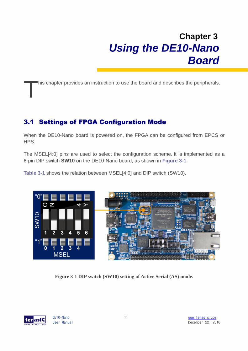
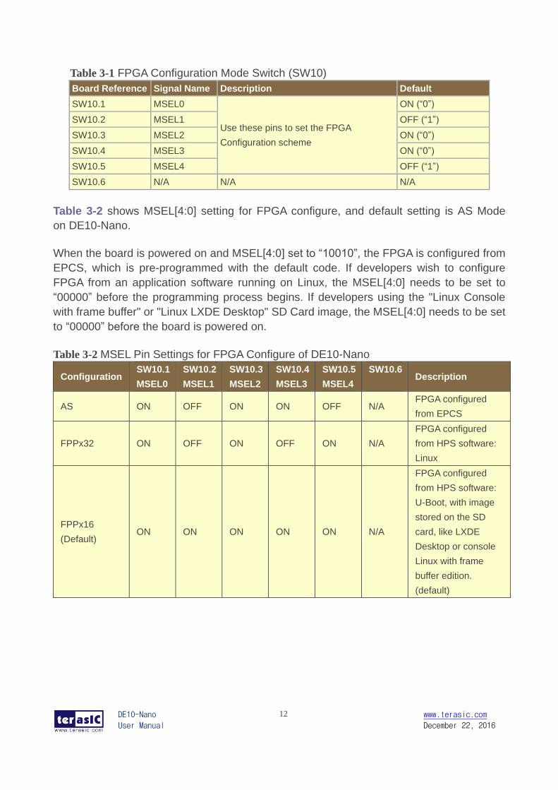
3.1 SSeettttiinnggss ooff FFPPGGAA CCoonnffiigguurraattiioonn MMooddee
When the DE10-Nano board is powered on, the FPGA can be configured from EPCS or
HPS.
The MSEL[4:0] pins are used to select the configuration scheme. It is implemented as a
6-pin DIP switch SW10 on the DE10-Nano board, as shown in Figure 3-1.
Table 3-1 shows the relation between MSEL[4:0] and DIP switch (SW10).
Figure 3-1 DIP switch (SW10) setting of Active Serial (AS) mode.
T
DE10-Nano
User Manual
12 www.terasic.com
December 22, 2016
Table 3-1 FPGA Configuration Mode Switch (SW10)
Board Reference Signal Name Description Default
SW10.1 MSEL0
Use these pins to set the FPGA
Configuration scheme
ON (“0”)
SW10.2 MSEL1 OFF (“1”)
SW10.3 MSEL2 ON (“0”)
SW10.4 MSEL3 ON (“0”)
SW10.5 MSEL4 OFF (“1”)
SW10.6 N/A N/A N/A
Table 3-2 shows MSEL[4:0] setting for FPGA configure, and default setting is AS Mode
on DE10-Nano.
When the board is powered on and MSEL[4:0] set to “10010”, the FPGA is configured from
EPCS, which is pre-programmed with the default code. If developers wish to configure
FPGA from an application software running on Linux, the MSEL[4:0] needs to be set to
“00000” before the programming process begins. If developers using the "Linux Console
with frame buffer" or "Linux LXDE Desktop" SD Card image, the MSEL[4:0] needs to be set
to “00000” before the board is powered on.
Table 3-2 MSEL Pin Settings for FPGA Configure of DE10-Nano
Configuration SW10.1
MSEL0
SW10.2
MSEL1
SW10.3
MSEL2
SW10.4
MSEL3
SW10.5
MSEL4
SW10.6
Description
AS ON OFF ON ON OFF N/A FPGA configured
from EPCS
FPPx32 ON OFF ON OFF ON N/A
FPGA configured
from HPS software:
Linux
FPPx16
(Default) ON ON ON ON ON N/A
FPGA configured
from HPS software:
U-Boot, with image
stored on the SD
card, like LXDE
Desktop or console
Linux with frame
buffer edition.
(default)
DE10-Nano
User Manual
13 www.terasic.com
December 22, 2016
3.2 CCoonnffiigguurraattiioonn ooff CCyycclloonnee VV SSooCC FFPPGGAA oonn DDEE1100--NNaannoo
There are two types of programming method supported by DE10-Nano:
1. JTAG programming: It is named after the IEEE standards Joint Test Action Group.
The configuration bit stream is downloaded directly into the Cyclone V SoC FPGA. The
FPGA will retain its current status as long as the power keeps applying to the board; the
configuration information will be lost when the power is off.
2. AS programming: The other programming method is Active Serial configuration.
The configuration bit stream is downloaded into the serial configuration device
(EPCS128), which provides non-volatile storage for the bit stream. The information is
retained within EPCS128 even if the DE10-Nano board is turned off. When the board is
powered on, the configuration data in the EPCS128 device is automatically loaded into
the Cyclone V SoC FPGA.
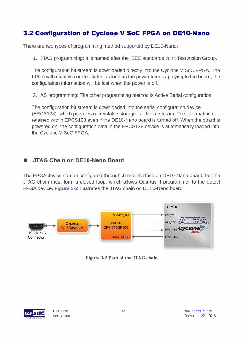
JTAG Chain on DE10-Nano Board
The FPGA device can be configured through JTAG interface on DE10-Nano board, but the
JTAG chain must form a closed loop, which allows Quartus II programmer to the detect
FPGA device. Figure 3-2 illustrates the JTAG chain on DE10-Nano board.
Figure 3-2 Path of the JTAG chain
DE10-Nano
User Manual
14 www.terasic.com
December 22, 2016
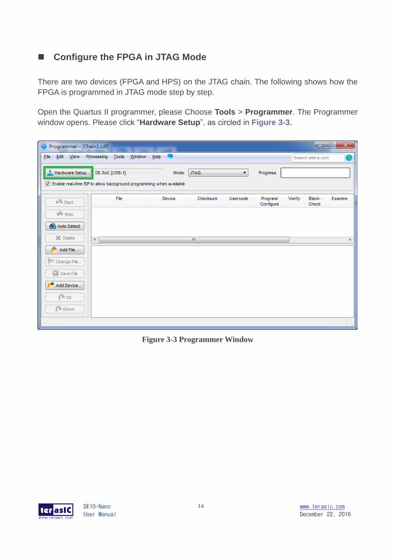
Configure the FPGA in JTAG Mode
There are two devices (FPGA and HPS) on the JTAG chain. The following shows how the
FPGA is programmed in JTAG mode step by step.
Open the Quartus II programmer, please Choose Tools > Programmer. The Programmer
window opens. Please click “Hardware Setup”, as circled in Figure 3-3.
Figure 3-3 Programmer Window
DE10-Nano
User Manual
15 www.terasic.com
December 22, 2016
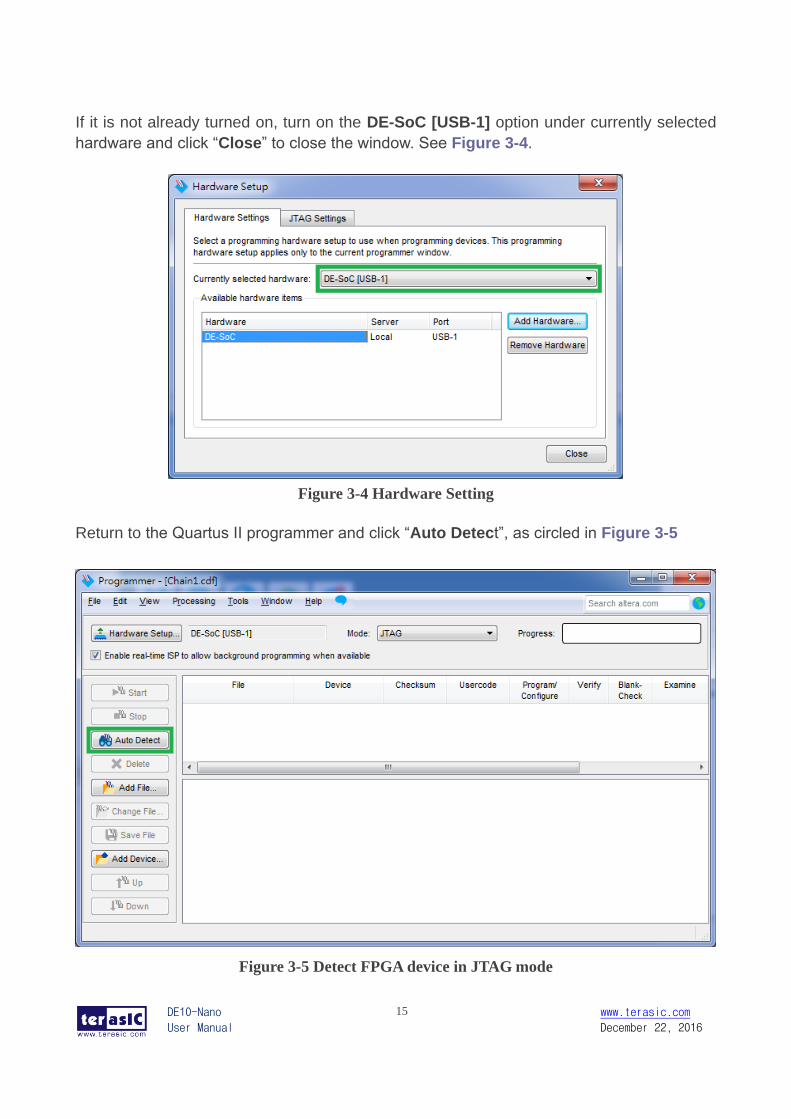
If it is not already turned on, turn on the DE-SoC [USB-1] option under currently selected
hardware and click “Close” to close the window. See Figure 3-4.
Figure 3-4 Hardware Setting
Return to the Quartus II programmer and click “Auto Detect”, as circled in Figure 3-5
Figure 3-5 Detect FPGA device in JTAG mode
DE10-Nano
User Manual
16 www.terasic.com
December 22, 2016
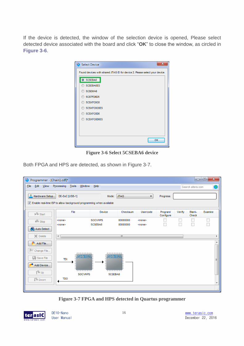
If the device is detected, the window of the selection device is opened, Please select
detected device associated with the board and click “OK” to close the window, as circled in
Figure 3-6.
Figure 3-6 Select 5CSEBA6 device
Both FPGA and HPS are detected, as shown in Figure 3-7.
Figure 3-7 FPGA and HPS detected in Quartus programmer
DE10-Nano
User Manual
17 www.terasic.com
December 22, 2016
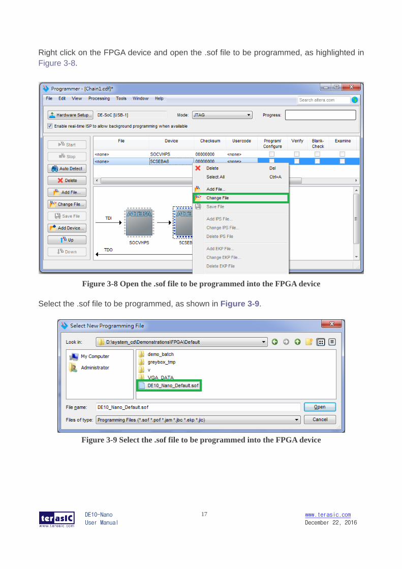
Right click on the FPGA device and open the .sof file to be programmed, as highlighted in
Figure 3-8.
Figure 3-8 Open the .sof file to be programmed into the FPGA device
Select the .sof file to be programmed, as shown in Figure 3-9.
Figure 3-9 Select the .sof file to be programmed into the FPGA device
DE10-Nano
User Manual
18 www.terasic.com
December 22, 2016
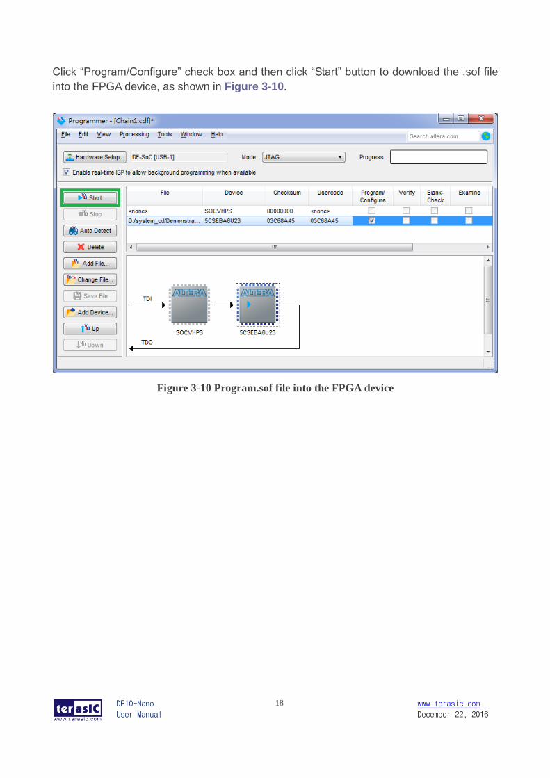
Click “Program/Configure” check box and then click “Start” button to download the .sof file
into the FPGA device, as shown in Figure 3-10.
Figure 3-10 Program.sof file into the FPGA device
DE10-Nano
User Manual
19 www.terasic.com
December 22, 2016
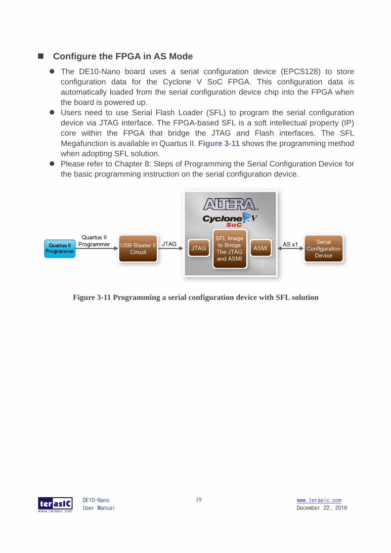
Configure the FPGA in AS Mode
The DE10-Nano board uses a serial configuration device (EPCS128) to store
configuration data for the Cyclone V SoC FPGA. This configuration data is
automatically loaded from the serial configuration device chip into the FPGA when
the board is powered up.
Users need to use Serial Flash Loader (SFL) to program the serial configuration
device via JTAG interface. The FPGA-based SFL is a soft intellectual property (IP)
core within the FPGA that bridge the JTAG and Flash interfaces. The SFL
Megafunction is available in Quartus II. Figure 3-11 shows the programming method
when adopting SFL solution.
Please refer to Chapter 8: Steps of Programming the Serial Configuration Device for
the basic programming instruction on the serial configuration device.
Figure 3-11 Programming a serial configuration device with SFL solution
DE10-Nano
User Manual
20 www.terasic.com
December 22, 2016
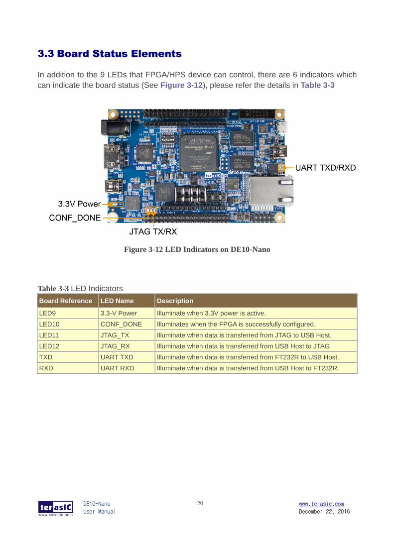
3.3 BBooaarrdd SSttaattuuss EElleemmeennttss
In addition to the 9 LEDs that FPGA/HPS device can control, there are 6 indicators which
can indicate the board status (See Figure 3-12), please refer the details in Table 3-3
Figure 3-12 LED Indicators on DE10-Nano
Table 3-3 LED Indicators
Board Reference LED Name Description
LED9 3.3-V Power Illuminate when 3.3V power is active.
LED10 CONF_DONE Illuminates when the FPGA is successfully configured.
LED11 JTAG_TX Illuminate when data is transferred from JTAG to USB Host.
LED12 JTAG_RX Illuminate when data is transferred from USB Host to JTAG.
TXD UART TXD Illuminate when data is transferred from FT232R to USB Host.
RXD UART RXD Illuminate when data is transferred from USB Host to FT232R.
DE10-Nano
User Manual
21 www.terasic.com
December 22, 2016
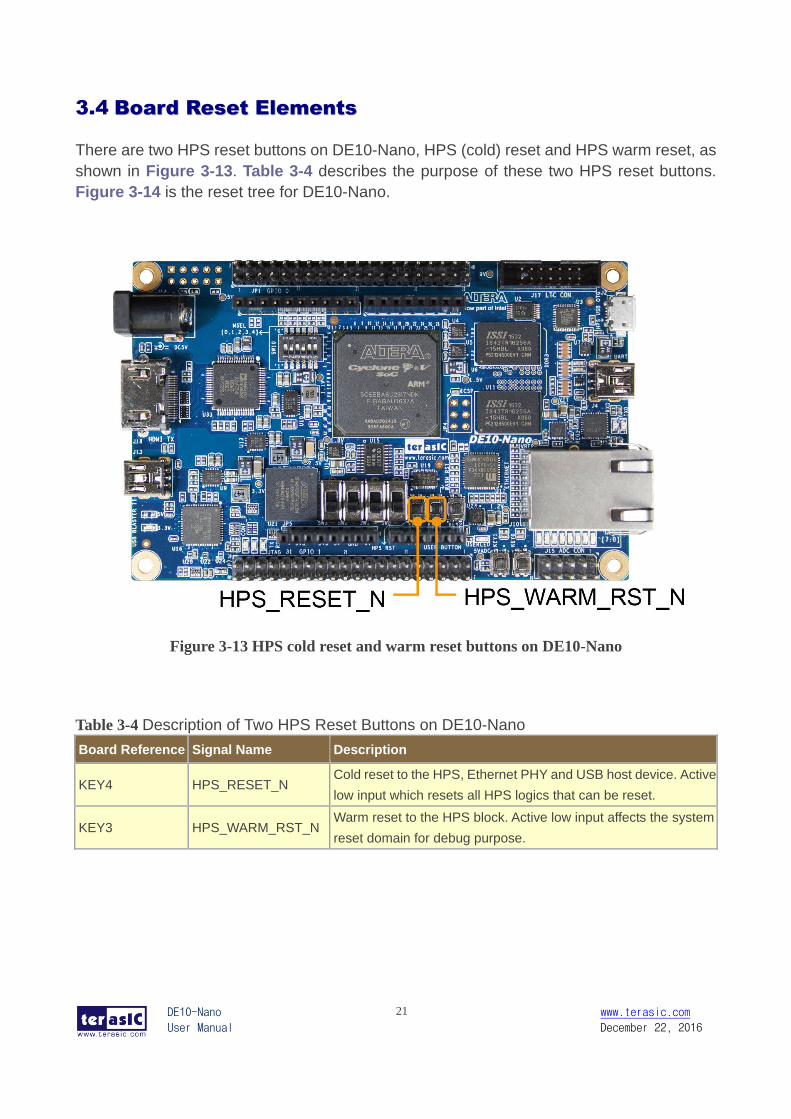
3.4 BBooaarrdd RReesseett EElleemmeennttss
There are two HPS reset buttons on DE10-Nano, HPS (cold) reset and HPS warm reset, as
shown in Figure 3-13. Table 3-4 describes the purpose of these two HPS reset buttons.
Figure 3-14 is the reset tree for DE10-Nano.
Figure 3-13 HPS cold reset and warm reset buttons on DE10-Nano
Table 3-4 Description of Two HPS Reset Buttons on DE10-Nano
Board Reference Signal Name Description
KEY4 HPS_RESET_N Cold reset to the HPS, Ethernet PHY and USB host device. Active
low input which resets all HPS logics that can be reset.
KEY3 HPS_WARM_RST_N Warm reset to the HPS block. Active low input affects the system
reset domain for debug purpose.
DE10-Nano
User Manual
22 www.terasic.com
December 22, 2016
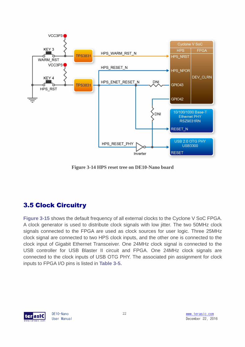
Figure 3-14 HPS reset tree on DE10-Nano board
3.5 CClloocckk CCiirrccuuiittrryy
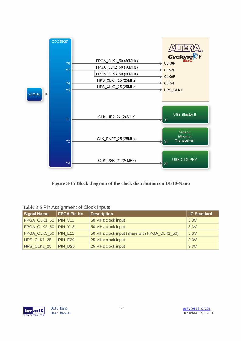
Figure 3-15 shows the default frequency of all external clocks to the Cyclone V SoC FPGA.
A clock generator is used to distribute clock signals with low jitter. The two 50MHz clock
signals connected to the FPGA are used as clock sources for user logic. Three 25MHz
clock signal are connected to two HPS clock inputs, and the other one is connected to the
clock input of Gigabit Ethernet Transceiver. One 24MHz clock signal is connected to the
USB controller for USB Blaster II circuit and FPGA. One 24MHz clock signals are
connected to the clock inputs of USB OTG PHY. The associated pin assignment for clock
inputs to FPGA I/O pins is listed in Table 3-5.
DE10-Nano
User Manual
23 www.terasic.com
December 22, 2016
Figure 3-15 Block diagram of the clock distribution on DE10-Nano
Table 3-5 Pin Assignment of Clock Inputs
Signal Name FPGA Pin No. Description I/O Standard
FPGA_CLK1_50 PIN_V11 50 MHz clock input 3.3V
FPGA_CLK2_50 PIN_Y13 50 MHz clock input 3.3V
FPGA_CLK3_50 PIN_E11 50 MHz clock input (share with FPGA_CLK1_50) 3.3V
HPS_CLK1_25 PIN_E20 25 MHz clock input 3.3V
HPS_CLK2_25 PIN_D20 25 MHz clock input 3.3V
DE10-Nano
User Manual
24 www.terasic.com
December 22, 2016
3.6 PPeerriipphheerraallss CCoonnnneecctteedd ttoo tthhee FFPPGGAA
This section describes the interfaces connected to the FPGA. Users can control or monitor different
interfaces with user logic from the FPGA.
33..66..11 UUsseerr PPuusshh--bbuuttttoonnss,, SSwwiittcchheess aanndd LLEEDDss
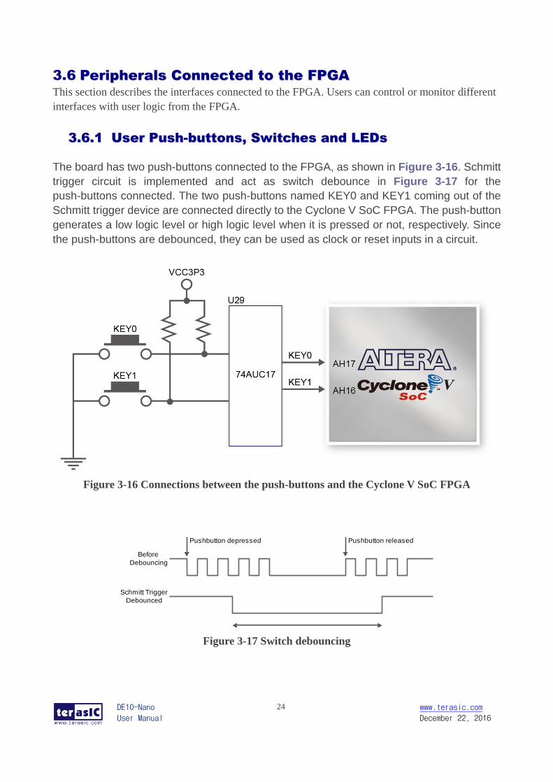
The board has two push-buttons connected to the FPGA, as shown in Figure 3-16. Schmitt
trigger circuit is implemented and act as switch debounce in Figure 3-17 for the
push-buttons connected. The two push-buttons named KEY0 and KEY1 coming out of the
Schmitt trigger device are connected directly to the Cyclone V SoC FPGA. The push-button
generates a low logic level or high logic level when it is pressed or not, respectively. Since
the push-buttons are debounced, they can be used as clock or reset inputs in a circuit.
Figure 3-16 Connections between the push-buttons and the Cyclone V SoC FPGA
Pushbutton releasedPushbutton depressed
Before
Debouncing
Schmitt Trigger
Debounced
Figure 3-17 Switch debouncing
DE10-Nano
User Manual
25 www.terasic.com
December 22, 2016
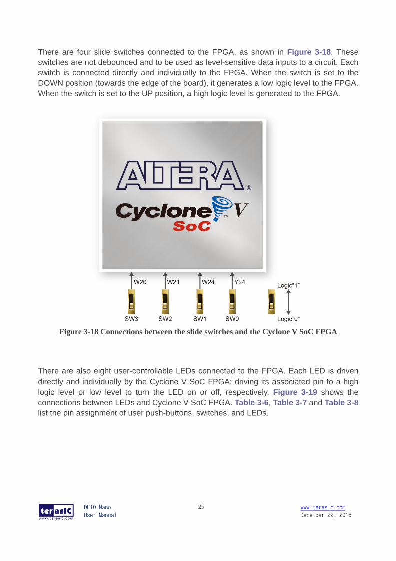
There are four slide switches connected to the FPGA, as shown in Figure 3-18. These
switches are not debounced and to be used as level-sensitive data inputs to a circuit. Each
switch is connected directly and individually to the FPGA. When the switch is set to the
DOWN position (towards the edge of the board), it generates a low logic level to the FPGA.
When the switch is set to the UP position, a high logic level is generated to the FPGA.
Figure 3-18 Connections between the slide switches and the Cyclone V SoC FPGA
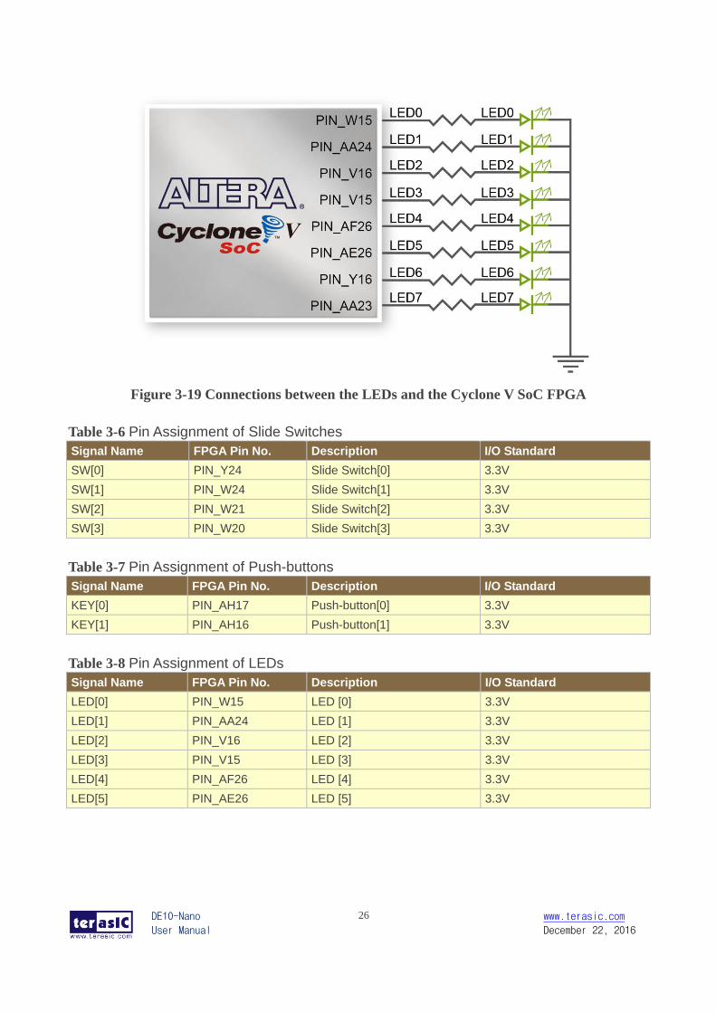
There are also eight user-controllable LEDs connected to the FPGA. Each LED is driven
directly and individually by the Cyclone V SoC FPGA; driving its associated pin to a high
logic level or low level to turn the LED on or off, respectively. Figure 3-19 shows the
connections between LEDs and Cyclone V SoC FPGA. Table 3-6, Table 3-7 and Table 3-8
list the pin assignment of user push-buttons, switches, and LEDs.
DE10-Nano
User Manual
26 www.terasic.com
December 22, 2016
Figure 3-19 Connections between the LEDs and the Cyclone V SoC FPGA
Table 3-6 Pin Assignment of Slide Switches
Signal Name FPGA Pin No. Description I/O Standard
SW[0] PIN_Y24 Slide Switch[0] 3.3V
SW[1] PIN_W24 Slide Switch[1] 3.3V
SW[2] PIN_W21 Slide Switch[2] 3.3V
SW[3] PIN_W20 Slide Switch[3] 3.3V
Table 3-7 Pin Assignment of Push-buttons
Signal Name FPGA Pin No. Description I/O Standard
KEY[0] PIN_AH17 Push-button[0] 3.3V
KEY[1] PIN_AH16 Push-button[1] 3.3V
Table 3-8 Pin Assignment of LEDs
Signal Name FPGA Pin No. Description I/O Standard
LED[0] PIN_W15 LED [0] 3.3V
LED[1] PIN_AA24 LED [1] 3.3V
LED[2] PIN_V16 LED [2] 3.3V
LED[3] PIN_V15 LED [3] 3.3V
LED[4] PIN_AF26 LED [4] 3.3V
LED[5] PIN_AE26 LED [5] 3.3V
DE10-Nano
User Manual
27 www.terasic.com
December 22, 2016
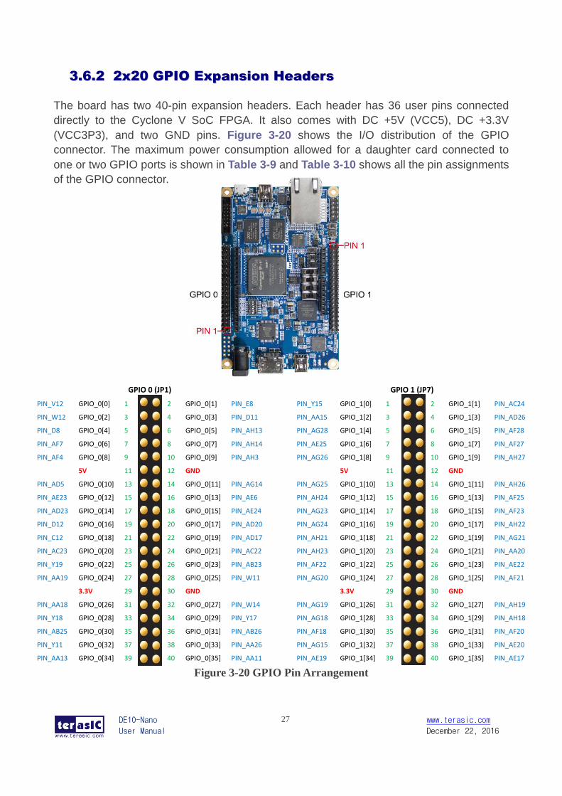
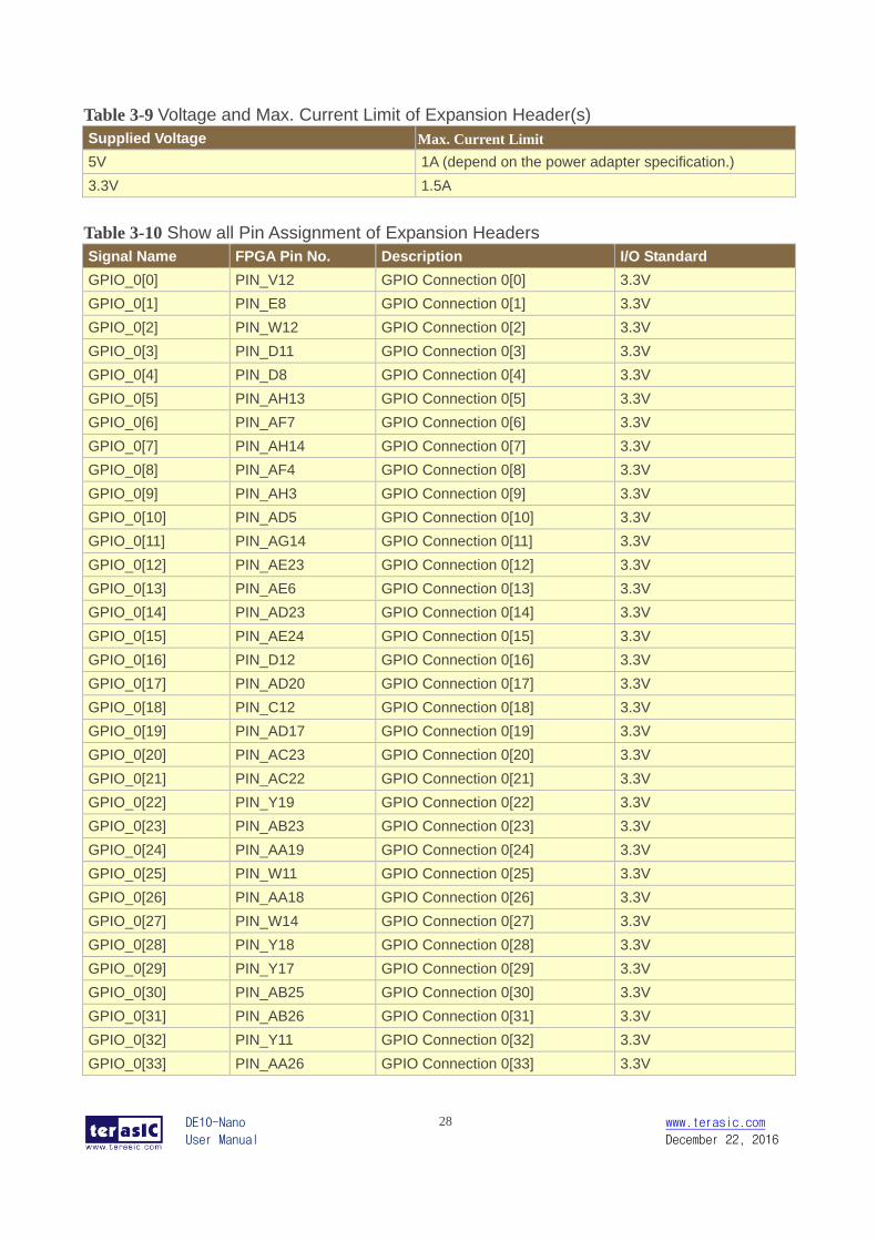
33..66..22 22xx2200 GGPPIIOO EExxppaannssiioonn HHeeaaddeerrss
The board has two 40-pin expansion headers. Each header has 36 user pins connected
directly to the Cyclone V SoC FPGA. It also comes with DC +5V (VCC5), DC +3.3V
(VCC3P3), and two GND pins. Figure 3-20 shows the I/O distribution of the GPIO
connector. The maximum power consumption allowed for a daughter card connected to
one or two GPIO ports is shown in Table 3-9 and Table 3-10 shows all the pin assignments
of the GPIO connector.
Figure 3-20 GPIO Pin Arrangement
GPIO 0 (JP1) GPIO 1 (JP7)
PIN_V12 GPIO_0[0] 1 2 GPIO_0[1] PIN_E8 PIN_Y15 GPIO_1[0] 1 2 GPIO_1[1] PIN_AC24
PIN_W12 GPIO_0[2] 3 4 GPIO_0[3] PIN_D11 PIN_AA15 GPIO_1[2] 3 4 GPIO_1[3] PIN_AD26
PIN_D8 GPIO_0[4] 5 6 GPIO_0[5] PIN_AH13 PIN_AG28 GPIO_1[4] 5 6 GPIO_1[5] PIN_AF28
PIN_AF7 GPIO_0[6] 7 8 GPIO_0[7] PIN_AH14 PIN_AE25 GPIO_1[6] 7 8 GPIO_1[7] PIN_AF27
PIN_AF4 GPIO_0[8] 9 10 GPIO_0[9] PIN_AH3 PIN_AG26 GPIO_1[8] 9 10 GPIO_1[9] PIN_AH27
5V 11 12 GND 5V 11 12 GND
PIN_AD5 GPIO_0[10] 13 14 GPIO_0[11] PIN_AG14 PIN_AG25 GPIO_1[10] 13 14 GPIO_1[11] PIN_AH26
PIN_AE23 GPIO_0[12] 15 16 GPIO_0[13] PIN_AE6 PIN_AH24 GPIO_1[12] 15 16 GPIO_1[13] PIN_AF25
PIN_AD23 GPIO_0[14] 17 18 GPIO_0[15] PIN_AE24 PIN_AG23 GPIO_1[14] 17 18 GPIO_1[15] PIN_AF23
PIN_D12 GPIO_0[16] 19 20 GPIO_0[17] PIN_AD20 PIN_AG24 GPIO_1[16] 19 20 GPIO_1[17] PIN_AH22
PIN_C12 GPIO_0[18] 21 22 GPIO_0[19] PIN_AD17 PIN_AH21 GPIO_1[18] 21 22 GPIO_1[19] PIN_AG21
PIN_AC23 GPIO_0[20] 23 24 GPIO_0[21] PIN_AC22 PIN_AH23 GPIO_1[20] 23 24 GPIO_1[21] PIN_AA20
PIN_Y19 GPIO_0[22] 25 26 GPIO_0[23] PIN_AB23 PIN_AF22 GPIO_1[22] 25 26 GPIO_1[23] PIN_AE22
PIN_AA19 GPIO_0[24] 27 28 GPIO_0[25] PIN_W11 PIN_AG20 GPIO_1[24] 27 28 GPIO_1[25] PIN_AF21
3.3V 29 30 GND 3.3V 29 30 GND
PIN_AA18 GPIO_0[26] 31 32 GPIO_0[27] PIN_W14 PIN_AG19 GPIO_1[26] 31 32 GPIO_1[27] PIN_AH19
PIN_Y18 GPIO_0[28] 33 34 GPIO_0[29] PIN_Y17 PIN_AG18 GPIO_1[28] 33 34 GPIO_1[29] PIN_AH18
PIN_AB25 GPIO_0[30] 35 36 GPIO_0[31] PIN_AB26 PIN_AF18 GPIO_1[30] 35 36 GPIO_1[31] PIN_AF20
PIN_Y11 GPIO_0[32] 37 38 GPIO_0[33] PIN_AA26 PIN_AG15 GPIO_1[32] 37 38 GPIO_1[33] PIN_AE20
PIN_AA13 GPIO_0[34] 39 40 GPIO_0[35] PIN_AA11 PIN_AE19 GPIO_1[34] 39 40 GPIO_1[35] PIN_AE17
DE10-Nano
User Manual
28 www.terasic.com
December 22, 2016
Table 3-9 Voltage and Max. Current Limit of Expansion Header(s)
Supplied Voltage Max. Current Limit
5V 1A (depend on the power adapter specification.)
3.3V 1.5A
Table 3-10 Show all Pin Assignment of Expansion Headers
Signal Name FPGA Pin No. Description I/O Standard
GPIO_0[0] PIN_V12 GPIO Connection 0[0] 3.3V
GPIO_0[1] PIN_E8 GPIO Connection 0[1] 3.3V
GPIO_0[2] PIN_W12 GPIO Connection 0[2] 3.3V
GPIO_0[3] PIN_D11 GPIO Connection 0[3] 3.3V
GPIO_0[4] PIN_D8 GPIO Connection 0[4] 3.3V
GPIO_0[5] PIN_AH13 GPIO Connection 0[5] 3.3V
GPIO_0[6] PIN_AF7 GPIO Connection 0[6] 3.3V
GPIO_0[7] PIN_AH14 GPIO Connection 0[7] 3.3V
GPIO_0[8] PIN_AF4 GPIO Connection 0[8] 3.3V
GPIO_0[9] PIN_AH3 GPIO Connection 0[9] 3.3V
GPIO_0[10] PIN_AD5 GPIO Connection 0[10] 3.3V
GPIO_0[11] PIN_AG14 GPIO Connection 0[11] 3.3V
GPIO_0[12] PIN_AE23 GPIO Connection 0[12] 3.3V
GPIO_0[13] PIN_AE6 GPIO Connection 0[13] 3.3V
GPIO_0[14] PIN_AD23 GPIO Connection 0[14] 3.3V
GPIO_0[15] PIN_AE24 GPIO Connection 0[15] 3.3V
GPIO_0[16] PIN_D12 GPIO Connection 0[16] 3.3V
GPIO_0[17] PIN_AD20 GPIO Connection 0[17] 3.3V
GPIO_0[18] PIN_C12 GPIO Connection 0[18] 3.3V
GPIO_0[19] PIN_AD17 GPIO Connection 0[19] 3.3V
GPIO_0[20] PIN_AC23 GPIO Connection 0[20] 3.3V
GPIO_0[21] PIN_AC22 GPIO Connection 0[21] 3.3V
GPIO_0[22] PIN_Y19 GPIO Connection 0[22] 3.3V
GPIO_0[23] PIN_AB23 GPIO Connection 0[23] 3.3V
GPIO_0[24] PIN_AA19 GPIO Connection 0[24] 3.3V
GPIO_0[25] PIN_W11 GPIO Connection 0[25] 3.3V
GPIO_0[26] PIN_AA18 GPIO Connection 0[26] 3.3V
GPIO_0[27] PIN_W14 GPIO Connection 0[27] 3.3V
GPIO_0[28] PIN_Y18 GPIO Connection 0[28] 3.3V
GPIO_0[29] PIN_Y17 GPIO Connection 0[29] 3.3V
GPIO_0[30] PIN_AB25 GPIO Connection 0[30] 3.3V
GPIO_0[31] PIN_AB26 GPIO Connection 0[31] 3.3V
GPIO_0[32] PIN_Y11 GPIO Connection 0[32] 3.3V
GPIO_0[33] PIN_AA26 GPIO Connection 0[33] 3.3V
DE10-Nano
User Manual
29 www.terasic.com
December 22, 2016
GPIO_0[34] PIN_AA13 GPIO Connection 0[34] 3.3V
GPIO_0[35] PIN_AA11 GPIO Connection 0[35] 3.3V
GPIO_1[0] PIN_Y15 GPIO Connection 1[0] 3.3V
GPIO_1[1] PIN_AC24 GPIO Connection 1[1] 3.3V
GPIO_1[2] PIN_AA15 GPIO Connection 1[2] 3.3V
GPIO_1[3] PIN_AD26 GPIO Connection 1[3] 3.3V
GPIO_1[4] PIN_AG28 GPIO Connection 1[4] 3.3V
GPIO_1[5] PIN_AF28 GPIO Connection 1[5] 3.3V
GPIO_1[6] PIN_AE25 GPIO Connection 1[6] 3.3V
GPIO_1[7] PIN_AF27 GPIO Connection 1[7] 3.3V
GPIO_1[8] PIN_AG26 GPIO Connection 1[8] 3.3V
GPIO_1[9] PIN_AH27 GPIO Connection 1[9] 3.3V
GPIO_1[10] PIN_AG25 GPIO Connection 1[10] 3.3V
GPIO_1[11] PIN_AH26 GPIO Connection 1[11] 3.3V
GPIO_1[12] PIN_AH24 GPIO Connection 1[12] 3.3V
GPIO_1[13] PIN_AF25 GPIO Connection 1[13] 3.3V
GPIO_1[14] PIN_AG23 GPIO Connection 1[14] 3.3V
GPIO_1[15] PIN_AF23 GPIO Connection 1[15] 3.3V
GPIO_1[16] PIN_AG24 GPIO Connection 1[16] 3.3V
GPIO_1[17] PIN_AH22 GPIO Connection 1[17] 3.3V
GPIO_1[18] PIN_AH21 GPIO Connection 1[18] 3.3V
GPIO_1[19] PIN_AG21 GPIO Connection 1[19] 3.3V
GPIO_1[20] PIN_AH23 GPIO Connection 1[20] 3.3V
GPIO_1[21] PIN_AA20 GPIO Connection 1[21] 3.3V
GPIO_1[22] PIN_AF22 GPIO Connection 1[22] 3.3V
GPIO_1[23] PIN_AE22 GPIO Connection 1[23] 3.3V
GPIO_1[24] PIN_AG20 GPIO Connection 1[24] 3.3V
GPIO_1[25] PIN_AF21 GPIO Connection 1[25] 3.3V
GPIO_1[26] PIN_AG19 GPIO Connection 1[26] 3.3V
GPIO_1[27] PIN_AH19 GPIO Connection 1[27] 3.3V
GPIO_1[28] PIN_AG18 GPIO Connection 1[28] 3.3V
GPIO_1[29] PIN_AH18 GPIO Connection 1[29] 3.3V
GPIO_1[30] PIN_AF18 GPIO Connection 1[30] 3.3V
GPIO_1[31] PIN_AF20 GPIO Connection 1[31] 3.3V
GPIO_1[32] PIN_AG15 GPIO Connection 1[32] 3.3V
GPIO_1[33] PIN_AE20 GPIO Connection 1[33] 3.3V
GPIO_1[34] PIN_AE19 GPIO Connection 1[34] 3.3V
GPIO_1[35] PIN_AE17 GPIO Connection 1[35] 3.3V
DE10-Nano
User Manual
30 www.terasic.com
December 22, 2016
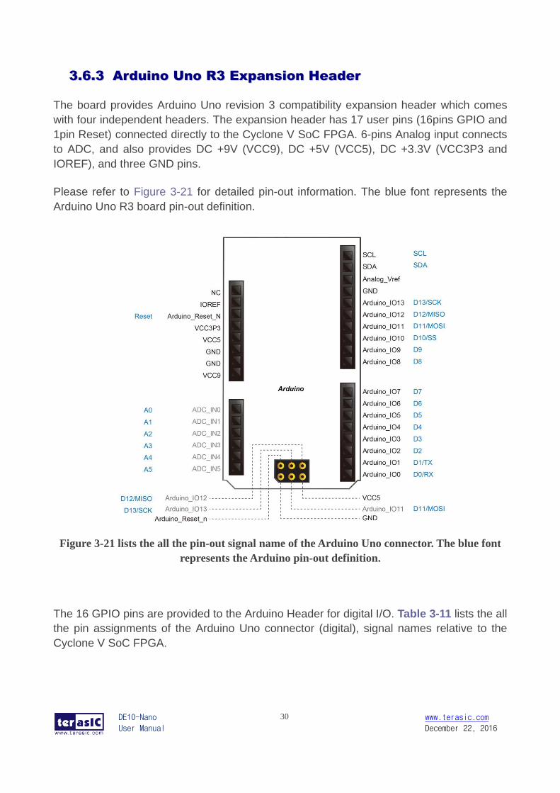
33..66..33 AArrdduuiinnoo UUnnoo RR33 EExxppaannssiioonn HHeeaaddeerr
The board provides Arduino Uno revision 3 compatibility expansion header which comes
with four independent headers. The expansion header has 17 user pins (16pins GPIO and
1pin Reset) connected directly to the Cyclone V SoC FPGA. 6-pins Analog input connects
to ADC, and also provides DC +9V (VCC9), DC +5V (VCC5), DC +3.3V (VCC3P3 and
IOREF), and three GND pins.
Please refer to Figure 3-21 for detailed pin-out information. The blue font represents the
Arduino Uno R3 board pin-out definition.
Figure 3-21 lists the all the pin-out signal name of the Arduino Uno connector. The blue font
represents the Arduino pin-out definition.
The 16 GPIO pins are provided to the Arduino Header for digital I/O. Table 3-11 lists the all
the pin assignments of the Arduino Uno connector (digital), signal names relative to the
Cyclone V SoC FPGA.
DE10-Nano
User Manual
31 www.terasic.com
December 22, 2016
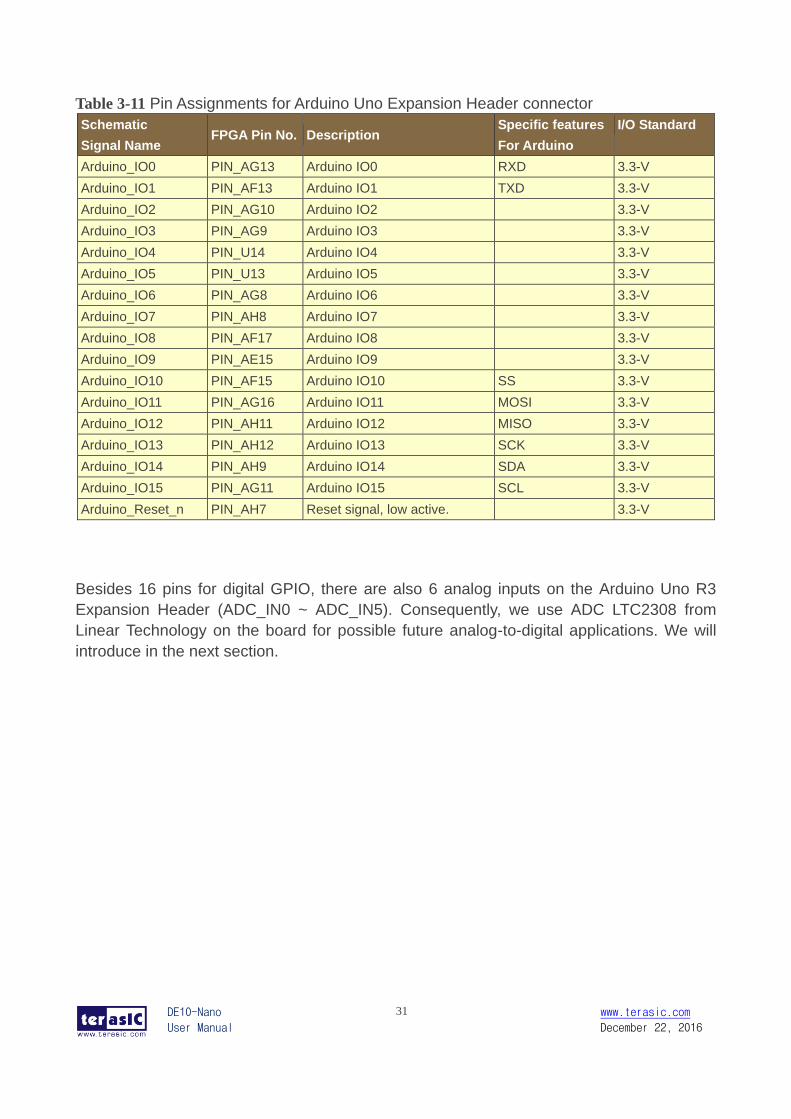
Table 3-11 Pin Assignments for Arduino Uno Expansion Header connector
Schematic
Signal Name FPGA Pin No. Description
Specific features
For Arduino
I/O Standard
Arduino_IO0 PIN_AG13 Arduino IO0 RXD 3.3-V
Arduino_IO1 PIN_AF13 Arduino IO1 TXD 3.3-V
Arduino_IO2 PIN_AG10 Arduino IO2 3.3-V
Arduino_IO3 PIN_AG9 Arduino IO3 3.3-V
Arduino_IO4 PIN_U14 Arduino IO4 3.3-V
Arduino_IO5 PIN_U13 Arduino IO5 3.3-V
Arduino_IO6 PIN_AG8 Arduino IO6 3.3-V
Arduino_IO7 PIN_AH8 Arduino IO7 3.3-V
Arduino_IO8 PIN_AF17 Arduino IO8 3.3-V
Arduino_IO9 PIN_AE15 Arduino IO9 3.3-V
Arduino_IO10 PIN_AF15 Arduino IO10 SS 3.3-V
Arduino_IO11 PIN_AG16 Arduino IO11 MOSI 3.3-V
Arduino_IO12 PIN_AH11 Arduino IO12 MISO 3.3-V
Arduino_IO13 PIN_AH12 Arduino IO13 SCK 3.3-V
Arduino_IO14 PIN_AH9 Arduino IO14 SDA 3.3-V
Arduino_IO15 PIN_AG11 Arduino IO15 SCL 3.3-V
Arduino_Reset_n PIN_AH7 Reset signal, low active. 3.3-V
Besides 16 pins for digital GPIO, there are also 6 analog inputs on the Arduino Uno R3
Expansion Header (ADC_IN0 ~ ADC_IN5). Consequently, we use ADC LTC2308 from
Linear Technology on the board for possible future analog-to-digital applications. We will
introduce in the next section.
DE10-Nano
User Manual
32 www.terasic.com
December 22, 2016
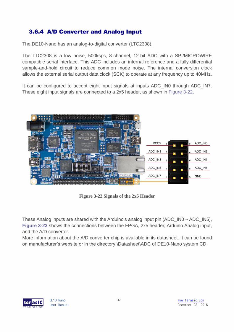
33..66..44 AA//DD CCoonnvveerrtteerr aanndd AAnnaalloogg IInnppuutt
The DE10-Nano has an analog-to-digital converter (LTC2308).
The LTC2308 is a low noise, 500ksps, 8-channel, 12-bit ADC with a SPI/MICROWIRE
compatible serial interface. This ADC includes an internal reference and a fully differential
sample-and-hold circuit to reduce common mode noise. The internal conversion clock
allows the external serial output data clock (SCK) to operate at any frequency up to 40MHz.
It can be configured to accept eight input signals at inputs ADC_IN0 through ADC_IN7.
These eight input signals are connected to a 2x5 header, as shown in Figure 3-22.
Figure 3-22 Signals of the 2x5 Header
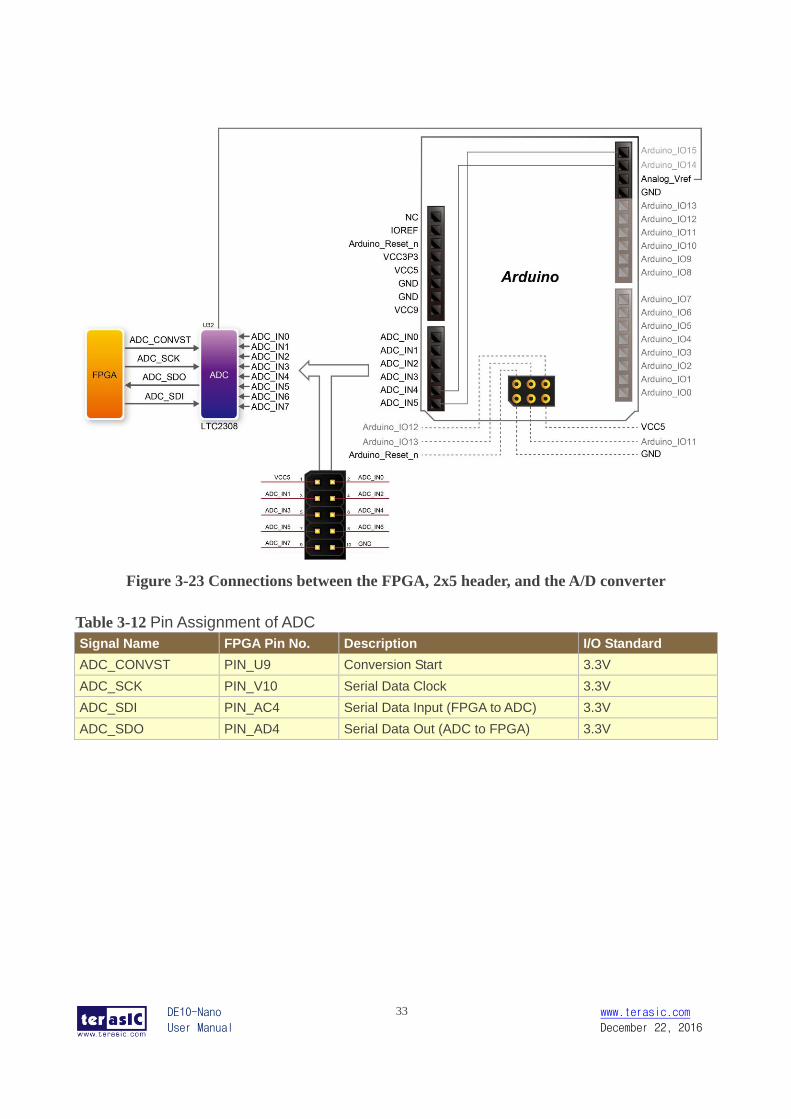
These Analog inputs are shared with the Arduino's analog input pin (ADC_IN0 ~ ADC_IN5),
Figure 3-23 shows the connections between the FPGA, 2x5 header, Arduino Analog input,
and the A/D converter.
More information about the A/D converter chip is available in its datasheet. It can be found
on manufacturer’s website or in the directory \Datasheet\ADC of DE10-Nano system CD.
DE10-Nano
User Manual
33 www.terasic.com
December 22, 2016
Figure 3-23 Connections between the FPGA, 2x5 header, and the A/D converter
Table 3-12 Pin Assignment of ADC
Signal Name FPGA Pin No. Description I/O Standard
ADC_CONVST PIN_U9 Conversion Start 3.3V
ADC_SCK PIN_V10 Serial Data Clock 3.3V
ADC_SDI PIN_AC4 Serial Data Input (FPGA to ADC) 3.3V
ADC_SDO PIN_AD4 Serial Data Out (ADC to FPGA) 3.3V
DE10-Nano
User Manual
34 www.terasic.com
December 22, 2016
33..66..55 HHDDMMII TTXX IInntteerrffaaccee
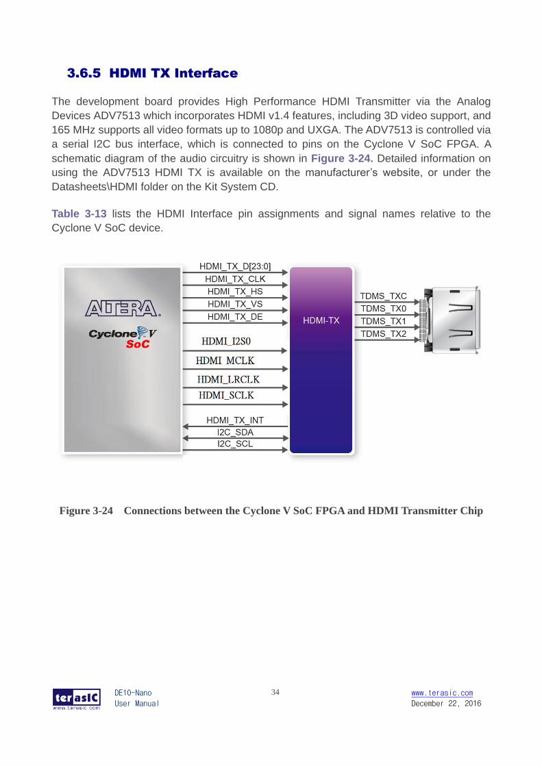
The development board provides High Performance HDMI Transmitter via the Analog
Devices ADV7513 which incorporates HDMI v1.4 features, including 3D video support, and
165 MHz supports all video formats up to 1080p and UXGA. The ADV7513 is controlled via
a serial I2C bus interface, which is connected to pins on the Cyclone V SoC FPGA. A
schematic diagram of the audio circuitry is shown in Figure 3-24. Detailed information on
using the ADV7513 HDMI TX is available on the manufacturer’s website, or under the
Datasheets\HDMI folder on the Kit System CD.
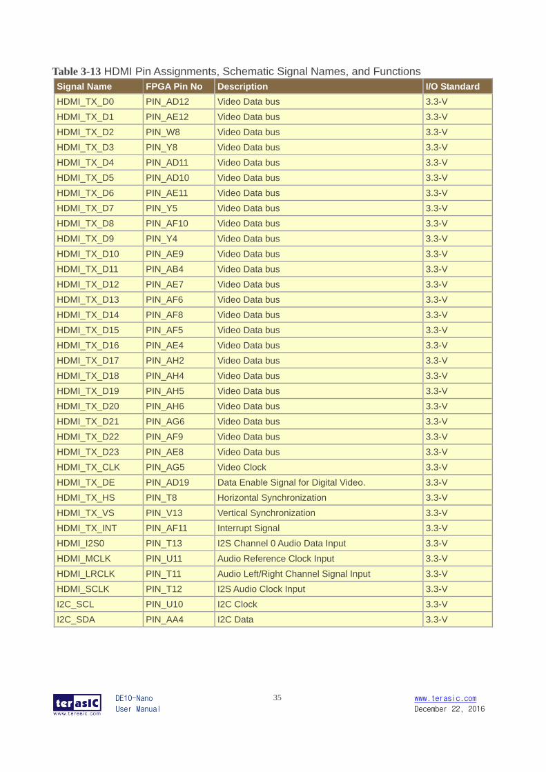
Table 3-13 lists the HDMI Interface pin assignments and signal names relative to the
Cyclone V SoC device.
Figure 3-24 Connections between the Cyclone V SoC FPGA and HDMI Transmitter Chip
DE10-Nano
User Manual
35 www.terasic.com
December 22, 2016
Table 3-13 HDMI Pin Assignments, Schematic Signal Names, and Functions
Signal Name FPGA Pin No Description I/O Standard
HDMI_TX_D0 PIN_AD12 Video Data bus 3.3-V
HDMI_TX_D1 PIN_AE12 Video Data bus 3.3-V
HDMI_TX_D2 PIN_W8 Video Data bus 3.3-V
HDMI_TX_D3 PIN_Y8 Video Data bus 3.3-V
HDMI_TX_D4 PIN_AD11 Video Data bus 3.3-V
HDMI_TX_D5 PIN_AD10 Video Data bus 3.3-V
HDMI_TX_D6 PIN_AE11 Video Data bus 3.3-V
HDMI_TX_D7 PIN_Y5 Video Data bus 3.3-V
HDMI_TX_D8 PIN_AF10 Video Data bus 3.3-V
HDMI_TX_D9 PIN_Y4 Video Data bus 3.3-V
HDMI_TX_D10 PIN_AE9 Video Data bus 3.3-V
HDMI_TX_D11 PIN_AB4 Video Data bus 3.3-V
HDMI_TX_D12 PIN_AE7 Video Data bus 3.3-V
HDMI_TX_D13 PIN_AF6 Video Data bus 3.3-V
HDMI_TX_D14 PIN_AF8 Video Data bus 3.3-V
HDMI_TX_D15 PIN_AF5 Video Data bus 3.3-V
HDMI_TX_D16 PIN_AE4 Video Data bus 3.3-V
HDMI_TX_D17 PIN_AH2 Video Data bus 3.3-V
HDMI_TX_D18 PIN_AH4 Video Data bus 3.3-V
HDMI_TX_D19 PIN_AH5 Video Data bus 3.3-V
HDMI_TX_D20 PIN_AH6 Video Data bus 3.3-V
HDMI_TX_D21 PIN_AG6 Video Data bus 3.3-V
HDMI_TX_D22 PIN_AF9 Video Data bus 3.3-V
HDMI_TX_D23 PIN_AE8 Video Data bus 3.3-V
HDMI_TX_CLK PIN_AG5 Video Clock 3.3-V
HDMI_TX_DE PIN_AD19 Data Enable Signal for Digital Video. 3.3-V
HDMI_TX_HS PIN_T8 Horizontal Synchronization 3.3-V
HDMI_TX_VS PIN_V13 Vertical Synchronization 3.3-V
HDMI_TX_INT PIN_AF11 Interrupt Signal 3.3-V
HDMI_I2S0 PIN_T13 I2S Channel 0 Audio Data Input 3.3-V
HDMI_MCLK PIN_U11 Audio Reference Clock Input 3.3-V
HDMI_LRCLK PIN_T11 Audio Left/Right Channel Signal Input 3.3-V
HDMI_SCLK PIN_T12 I2S Audio Clock Input 3.3-V
I2C_SCL PIN_U10 I2C Clock 3.3-V
I2C_SDA PIN_AA4 I2C Data 3.3-V
DE10-Nano
User Manual
36 www.terasic.com
December 22, 2016
3.7 PPeerriipphheerraallss CCoonnnneecctteedd ttoo HHaarrdd PPrroocceessssoorr SSyysstteemm ((HHPPSS))
This section introduces the interfaces connected to the HPS section of the Cyclone V SoC FPGA.
Users can access these interfaces via the HPS processor.
33..77..11 UUsseerr PPuusshh--bbuuttttoonnss aanndd LLEEDDss
Similar to the FPGA, the HPS also has its set of switches, buttons, LEDs, and other
interfaces connected exclusively. Users can control these interfaces to monitor the status of
HPS.
Table 3-14 gives the pin assignment of all the LEDs, switches, and push-buttons.
Table 3-14 Pin Assignment of LEDs, Switches and Push-buttons
Signal Nam FPGA Pin No HPS GPIO Register/bit Function
HPS_KEY PIN_J18 GPIO54 GPIO1[25] I/O
HPS_LED PIN_A20 GPIO53 GPIO1[24] I/O
33..77..22 GGiiggaabbiitt EEtthheerrnneett
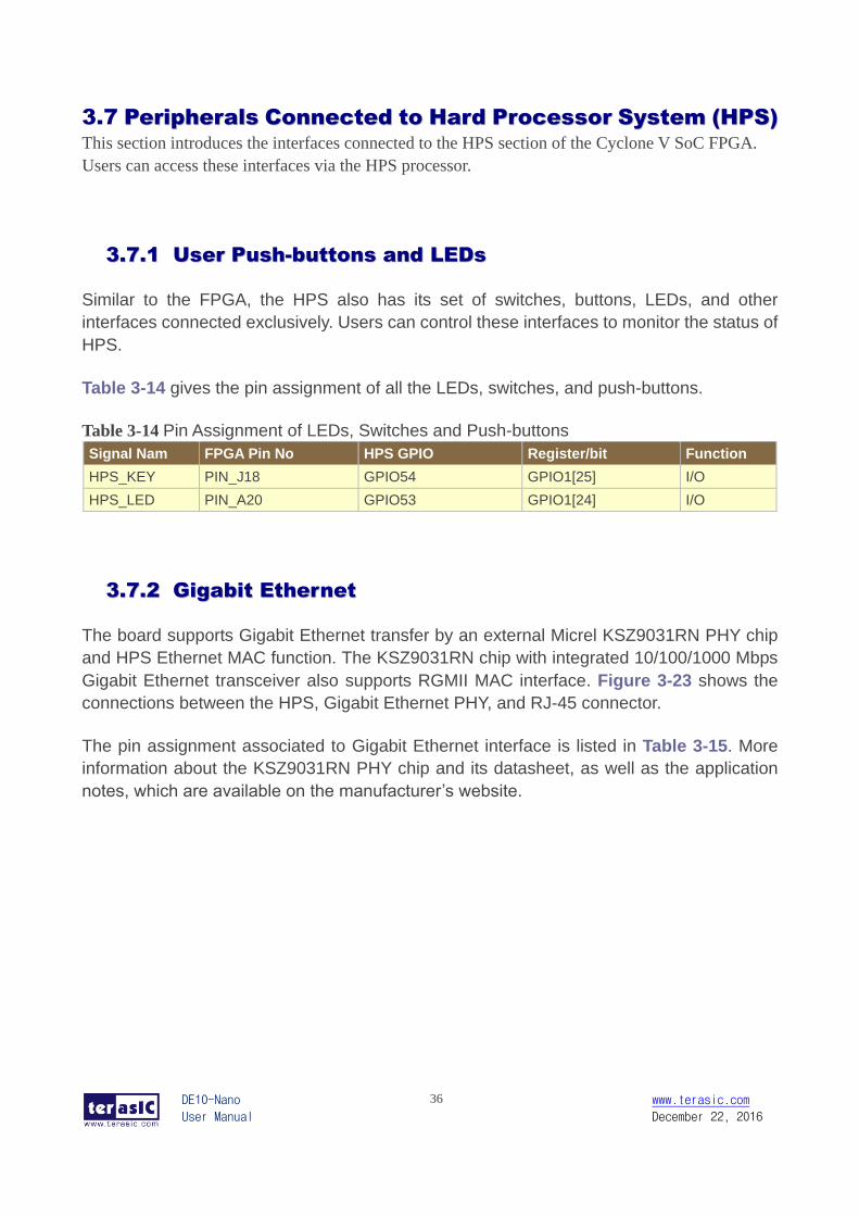
The board supports Gigabit Ethernet transfer by an external Micrel KSZ9031RN PHY chip
and HPS Ethernet MAC function. The KSZ9031RN chip with integrated 10/100/1000 Mbps
Gigabit Ethernet transceiver also supports RGMII MAC interface. Figure 3-23 shows the
connections between the HPS, Gigabit Ethernet PHY, and RJ-45 connector.
The pin assignment associated to Gigabit Ethernet interface is listed in Table 3-15. More
information about the KSZ9031RN PHY chip and its datasheet, as well as the application
notes, which are available on the manufacturer’s website.
DE10-Nano
User Manual
37 www.terasic.com
December 22, 2016
Figure 3-23 Connections between the HPS and Gigabit Ethernet
Table 3-15 Pin Assignment of Gigabit Ethernet PHY
Signal Name FPGA Pin No Description I/O Standard
HPS_ENET_TX_EN PIN_A12 GMII and MII transmit enable 3.3V
HPS_ENET_TX_DATA[0] PIN_A16 MII transmit data[0] 3.3V
HPS_ENET_TX_DATA[1] PIN_J14 MII transmit data[1] 3.3V
HPS_ENET_TX_DATA[2] PIN_A15 MII transmit data[2] 3.3V
HPS_ENET_TX_DATA[3] PIN_D17 MII transmit data[3] 3.3V
HPS_ENET_RX_DV PIN_J13 GMII and MII receive data valid 3.3V
HPS_ENET_RX_DATA[0] PIN_A14 GMII and MII receive data[0] 3.3V
HPS_ENET_RX_DATA[1] PIN_A11 GMII and MII receive data[1] 3.3V
HPS_ENET_RX_DATA[2] PIN_C15 GMII and MII receive data[2] 3.3V
HPS_ENET_RX_DATA[3] PIN_A9 GMII and MII receive data[3] 3.3V
HPS_ENET_RX_CLK PIN_J12 GMII and MII receive clock 3.3V
HPS_ENET_RESET_N PIN_B14 Hardware Reset Signal 3.3V
HPS_ENET_MDIO PIN_E16 Management Data 3.3V
HPS_ENET_MDC PIN_A13 Management Data Clock Reference 3.3V
HPS_ENET_INT_N PIN_B14 Interrupt Open Drain Output 3.3V
HPS_ENET_GTX_CLK PIN_J15 GMII Transmit Clock 3.3V
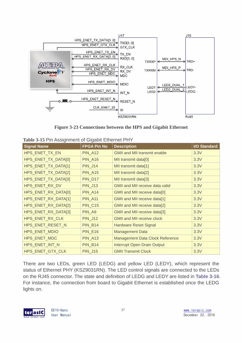
There are two LEDs, green LED (LEDG) and yellow LED (LEDY), which represent the
status of Ethernet PHY (KSZ9031RN). The LED control signals are connected to the LEDs
on the RJ45 connector. The state and definition of LEDG and LEDY are listed in Table 3-16.
For instance, the connection from board to Gigabit Ethernet is established once the LEDG
lights on.
DE10-Nano
User Manual
38 www.terasic.com
December 22, 2016
Table 3-16 State and Definition of LED Mode Pins
LED (State) LED (Definition) Link /Activity
LEDG LEDY LEDG LEDY
H H OFF OFF Link off
L H ON OFF 1000 Link / No Activity
Toggle H Blinking OFF 1000 Link / Activity (RX, TX)
H L OFF ON 100 Link / No Activity
H Toggle OFF Blinking 100 Link / Activity (RX, TX)
L L ON ON 10 Link/ No Activity
Toggle Toggle Blinking Blinking Link / Activity (RX, TX)
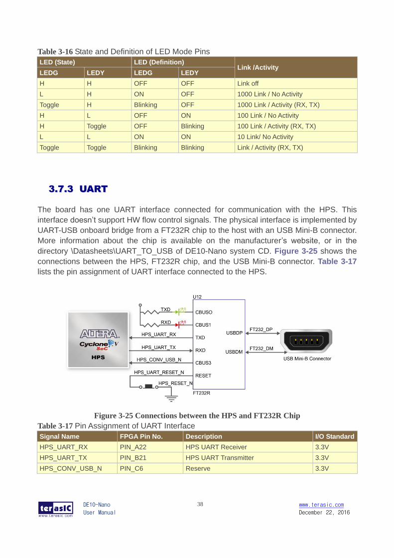
33..77..33 UUAARRTT
The board has one UART interface connected for communication with the HPS. This
interface doesn’t support HW flow control signals. The physical interface is implemented by
UART-USB onboard bridge from a FT232R chip to the host with an USB Mini-B connector.
More information about the chip is available on the manufacturer’s website, or in the
directory \Datasheets\UART_TO_USB of DE10-Nano system CD. Figure 3-25 shows the
connections between the HPS, FT232R chip, and the USB Mini-B connector. Table 3-17
lists the pin assignment of UART interface connected to the HPS.
Figure 3-25 Connections between the HPS and FT232R Chip
Table 3-17 Pin Assignment of UART Interface
Signal Name FPGA Pin No. Description I/O Standard
HPS_UART_RX PIN_A22 HPS UART Receiver 3.3V
HPS_UART_TX PIN_B21 HPS UART Transmitter 3.3V
HPS_CONV_USB_N PIN_C6 Reserve 3.3V
DE10-Nano
User Manual
39 www.terasic.com
December 22, 2016
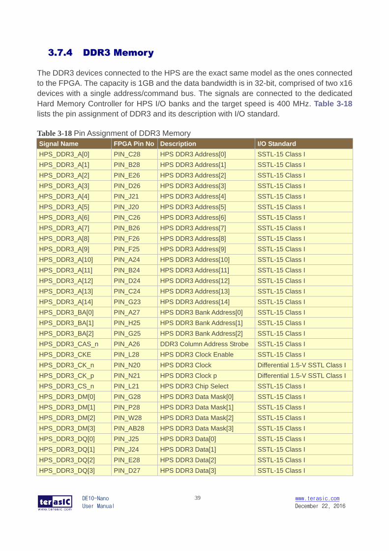
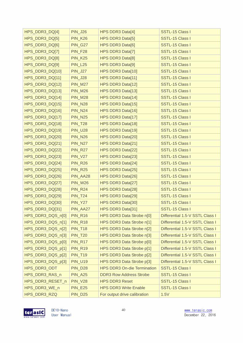
33..77..44 DDDDRR33 MMeemmoorryy
The DDR3 devices connected to the HPS are the exact same model as the ones connected
to the FPGA. The capacity is 1GB and the data bandwidth is in 32-bit, comprised of two x16
devices with a single address/command bus. The signals are connected to the dedicated
Hard Memory Controller for HPS I/O banks and the target speed is 400 MHz. Table 3-18
lists the pin assignment of DDR3 and its description with I/O standard.
Table 3-18 Pin Assignment of DDR3 Memory
Signal Name FPGA Pin No Description I/O Standard
HPS_DDR3_A[0] PIN_C28 HPS DDR3 Address[0] SSTL-15 Class I
HPS_DDR3_A[1] PIN_B28 HPS DDR3 Address[1] SSTL-15 Class I
HPS_DDR3_A[2] PIN_E26 HPS DDR3 Address[2] SSTL-15 Class I
HPS_DDR3_A[3] PIN_D26 HPS DDR3 Address[3] SSTL-15 Class I
HPS_DDR3_A[4] PIN_J21 HPS DDR3 Address[4] SSTL-15 Class I
HPS_DDR3_A[5] PIN_J20 HPS DDR3 Address[5] SSTL-15 Class I
HPS_DDR3_A[6] PIN_C26 HPS DDR3 Address[6] SSTL-15 Class I
HPS_DDR3_A[7] PIN_B26 HPS DDR3 Address[7] SSTL-15 Class I
HPS_DDR3_A[8] PIN_F26 HPS DDR3 Address[8] SSTL-15 Class I
HPS_DDR3_A[9] PIN_F25 HPS DDR3 Address[9] SSTL-15 Class I
HPS_DDR3_A[10] PIN_A24 HPS DDR3 Address[10] SSTL-15 Class I
HPS_DDR3_A[11] PIN_B24 HPS DDR3 Address[11] SSTL-15 Class I
HPS_DDR3_A[12] PIN_D24 HPS DDR3 Address[12] SSTL-15 Class I
HPS_DDR3_A[13] PIN_C24 HPS DDR3 Address[13] SSTL-15 Class I
HPS_DDR3_A[14] PIN_G23 HPS DDR3 Address[14] SSTL-15 Class I
HPS_DDR3_BA[0] PIN_A27 HPS DDR3 Bank Address[0] SSTL-15 Class I
HPS_DDR3_BA[1] PIN_H25 HPS DDR3 Bank Address[1] SSTL-15 Class I
HPS_DDR3_BA[2] PIN_G25 HPS DDR3 Bank Address[2] SSTL-15 Class I
HPS_DDR3_CAS_n PIN_A26 DDR3 Column Address Strobe SSTL-15 Class I
HPS_DDR3_CKE PIN_L28 HPS DDR3 Clock Enable SSTL-15 Class I
HPS_DDR3_CK_n PIN_N20 HPS DDR3 Clock Differential 1.5-V SSTL Class I
HPS_DDR3_CK_p PIN_N21 HPS DDR3 Clock p Differential 1.5-V SSTL Class I
HPS_DDR3_CS_n PIN_L21 HPS DDR3 Chip Select SSTL-15 Class I
HPS_DDR3_DM[0] PIN_G28 HPS DDR3 Data Mask[0] SSTL-15 Class I
HPS_DDR3_DM[1] PIN_P28 HPS DDR3 Data Mask[1] SSTL-15 Class I
HPS_DDR3_DM[2] PIN_W28 HPS DDR3 Data Mask[2] SSTL-15 Class I
HPS_DDR3_DM[3] PIN_AB28 HPS DDR3 Data Mask[3] SSTL-15 Class I
HPS_DDR3_DQ[0] PIN_J25 HPS DDR3 Data[0] SSTL-15 Class I
HPS_DDR3_DQ[1] PIN_J24 HPS DDR3 Data[1] SSTL-15 Class I
HPS_DDR3_DQ[2] PIN_E28 HPS DDR3 Data[2] SSTL-15 Class I
HPS_DDR3_DQ[3] PIN_D27 HPS DDR3 Data[3] SSTL-15 Class I
DE10-Nano
User Manual
40 www.terasic.com
December 22, 2016
HPS_DDR3_DQ[4] PIN_J26 HPS DDR3 Data[4] SSTL-15 Class I
HPS_DDR3_DQ[5] PIN_K26 HPS DDR3 Data[5] SSTL-15 Class I
HPS_DDR3_DQ[6] PIN_G27 HPS DDR3 Data[6] SSTL-15 Class I
HPS_DDR3_DQ[7] PIN_F28 HPS DDR3 Data[7] SSTL-15 Class I
HPS_DDR3_DQ[8] PIN_K25 HPS DDR3 Data[8] SSTL-15 Class I
HPS_DDR3_DQ[9] PIN_L25 HPS DDR3 Data[9] SSTL-15 Class I
HPS_DDR3_DQ[10] PIN_J27 HPS DDR3 Data[10] SSTL-15 Class I
HPS_DDR3_DQ[11] PIN_J28 HPS DDR3 Data[11] SSTL-15 Class I
HPS_DDR3_DQ[12] PIN_M27 HPS DDR3 Data[12] SSTL-15 Class I
HPS_DDR3_DQ[13] PIN_M26 HPS DDR3 Data[13] SSTL-15 Class I
HPS_DDR3_DQ[14] PIN_M28 HPS DDR3 Data[14] SSTL-15 Class I
HPS_DDR3_DQ[15] PIN_N28 HPS DDR3 Data[15] SSTL-15 Class I
HPS_DDR3_DQ[16] PIN_N24 HPS DDR3 Data[16] SSTL-15 Class I
HPS_DDR3_DQ[17] PIN_N25 HPS DDR3 Data[17] SSTL-15 Class I
HPS_DDR3_DQ[18] PIN_T28 HPS DDR3 Data[18] SSTL-15 Class I
HPS_DDR3_DQ[19] PIN_U28 HPS DDR3 Data[19] SSTL-15 Class I
HPS_DDR3_DQ[20] PIN_N26 HPS DDR3 Data[20] SSTL-15 Class I
HPS_DDR3_DQ[21] PIN_N27 HPS DDR3 Data[21] SSTL-15 Class I
HPS_DDR3_DQ[22] PIN_R27 HPS DDR3 Data[22] SSTL-15 Class I
HPS_DDR3_DQ[23] PIN_V27 HPS DDR3 Data[23] SSTL-15 Class I
HPS_DDR3_DQ[24] PIN_R26 HPS DDR3 Data[24] SSTL-15 Class I
HPS_DDR3_DQ[25] PIN_R25 HPS DDR3 Data[25] SSTL-15 Class I
HPS_DDR3_DQ[26] PIN_AA28 HPS DDR3 Data[26] SSTL-15 Class I
HPS_DDR3_DQ[27] PIN_W26 HPS DDR3 Data[27] SSTL-15 Class I
HPS_DDR3_DQ[28] PIN_R24 HPS DDR3 Data[28] SSTL-15 Class I
HPS_DDR3_DQ[29] PIN_T24 HPS DDR3 Data[29] SSTL-15 Class I
HPS_DDR3_DQ[30] PIN_Y27 HPS DDR3 Data[30] SSTL-15 Class I
HPS_DDR3_DQ[31] PIN_AA27 HPS DDR3 Data[31] SSTL-15 Class I
HPS_DDR3_DQS_n[0] PIN_R16 HPS DDR3 Data Strobe n[0] Differential 1.5-V SSTL Class I
HPS_DDR3_DQS_n[1] PIN_R18 HPS DDR3 Data Strobe n[1] Differential 1.5-V SSTL Class I
HPS_DDR3_DQS_n[2] PIN_T18 HPS DDR3 Data Strobe n[2] Differential 1.5-V SSTL Class I
HPS_DDR3_DQS_n[3] PIN_T20 HPS DDR3 Data Strobe n[3] Differential 1.5-V SSTL Class I
HPS_DDR3_DQS_p[0] PIN_R17 HPS DDR3 Data Strobe p[0] Differential 1.5-V SSTL Class I
HPS_DDR3_DQS_p[1] PIN_R19 HPS DDR3 Data Strobe p[1] Differential 1.5-V SSTL Class I
HPS_DDR3_DQS_p[2] PIN_T19 HPS DDR3 Data Strobe p[2] Differential 1.5-V SSTL Class I
HPS_DDR3_DQS_p[3] PIN_U19 HPS DDR3 Data Strobe p[3] Differential 1.5-V SSTL Class I
HPS_DDR3_ODT PIN_D28 HPS DDR3 On-die Termination SSTL-15 Class I
HPS_DDR3_RAS_n PIN_A25 DDR3 Row Address Strobe SSTL-15 Class I
HPS_DDR3_RESET_n PIN_V28 HPS DDR3 Reset SSTL-15 Class I
HPS_DDR3_WE_n PIN_E25 HPS DDR3 Write Enable SSTL-15 Class I
HPS_DDR3_RZQ PIN_D25 For output drive calibration 1.5V
DE10-Nano
User Manual
41 www.terasic.com
December 22, 2016
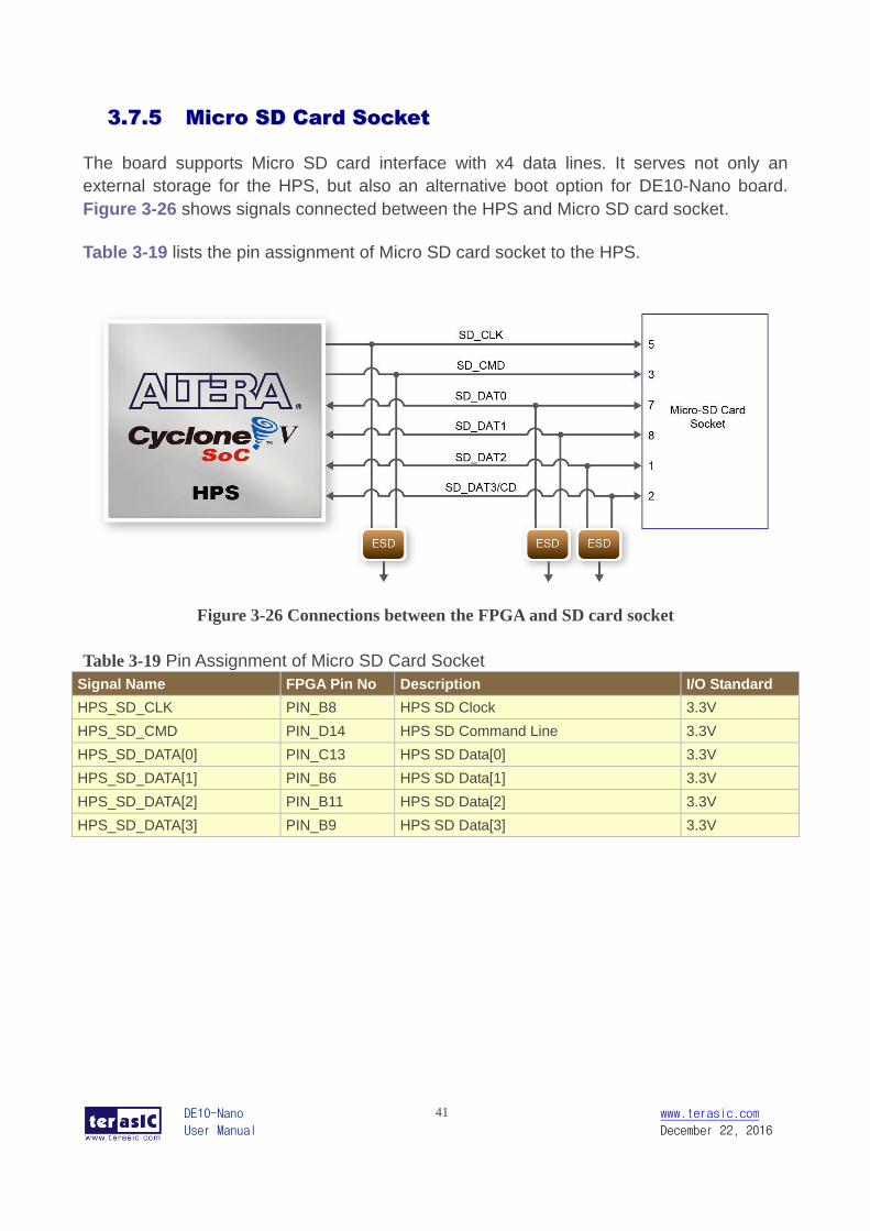
33..77..55 MMiiccrroo SSDD CCaarrdd SSoocckkeett
The board supports Micro SD card interface with x4 data lines. It serves not only an
external storage for the HPS, but also an alternative boot option for DE10-Nano board.
Figure 3-26 shows signals connected between the HPS and Micro SD card socket.
Table 3-19 lists the pin assignment of Micro SD card socket to the HPS.
Figure 3-26 Connections between the FPGA and SD card socket
Table 3-19 Pin Assignment of Micro SD Card Socket
Signal Name FPGA Pin No Description I/O Standard
HPS_SD_CLK PIN_B8 HPS SD Clock 3.3V
HPS_SD_CMD PIN_D14 HPS SD Command Line 3.3V
HPS_SD_DATA[0] PIN_C13 HPS SD Data[0] 3.3V
HPS_SD_DATA[1] PIN_B6 HPS SD Data[1] 3.3V
HPS_SD_DATA[2] PIN_B11 HPS SD Data[2] 3.3V
HPS_SD_DATA[3] PIN_B9 HPS SD Data[3] 3.3V
DE10-Nano
User Manual
42 www.terasic.com
December 22, 2016
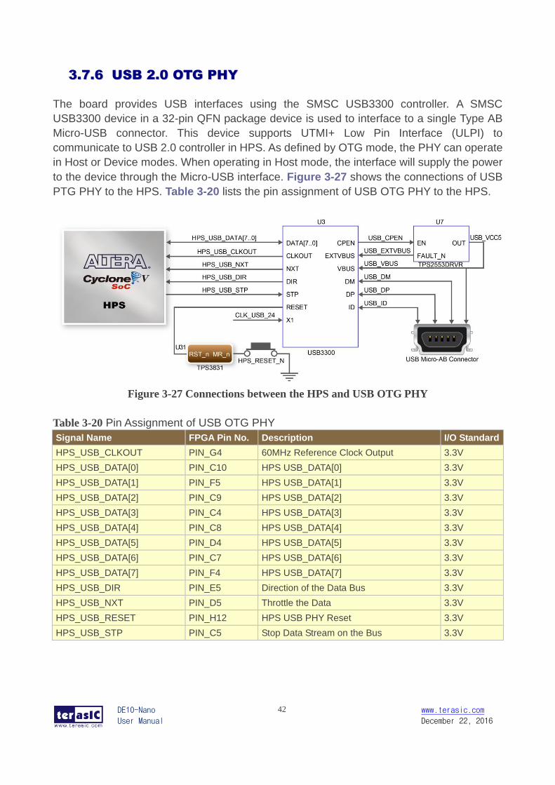
33..77..66 UUSSBB 22..00 OOTTGG PPHHYY
The board provides USB interfaces using the SMSC USB3300 controller. A SMSC
USB3300 device in a 32-pin QFN package device is used to interface to a single Type AB
Micro-USB connector. This device supports UTMI+ Low Pin Interface (ULPI) to
communicate to USB 2.0 controller in HPS. As defined by OTG mode, the PHY can operate
in Host or Device modes. When operating in Host mode, the interface will supply the power
to the device through the Micro-USB interface. Figure 3-27 shows the connections of USB
PTG PHY to the HPS. Table 3-20 lists the pin assignment of USB OTG PHY to the HPS.
Figure 3-27 Connections between the HPS and USB OTG PHY
Table 3-20 Pin Assignment of USB OTG PHY
Signal Name FPGA Pin No. Description I/O Standard
HPS_USB_CLKOUT PIN_G4 60MHz Reference Clock Output 3.3V
HPS_USB_DATA[0] PIN_C10 HPS USB_DATA[0] 3.3V
HPS_USB_DATA[1] PIN_F5 HPS USB_DATA[1] 3.3V
HPS_USB_DATA[2] PIN_C9 HPS USB_DATA[2] 3.3V
HPS_USB_DATA[3] PIN_C4 HPS USB_DATA[3] 3.3V
HPS_USB_DATA[4] PIN_C8 HPS USB_DATA[4] 3.3V
HPS_USB_DATA[5] PIN_D4 HPS USB_DATA[5] 3.3V
HPS_USB_DATA[6] PIN_C7 HPS USB_DATA[6] 3.3V
HPS_USB_DATA[7] PIN_F4 HPS USB_DATA[7] 3.3V
HPS_USB_DIR PIN_E5 Direction of the Data Bus 3.3V
HPS_USB_NXT PIN_D5 Throttle the Data 3.3V
HPS_USB_RESET PIN_H12 HPS USB PHY Reset 3.3V
HPS_USB_STP PIN_C5 Stop Data Stream on the Bus 3.3V
DE10-Nano
User Manual
43 www.terasic.com
December 22, 2016
33..77..77 GG--sseennssoorr
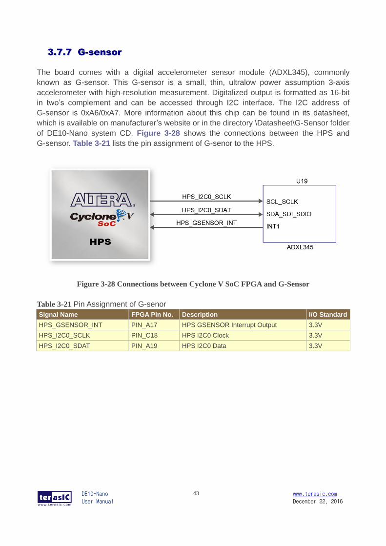
The board comes with a digital accelerometer sensor module (ADXL345), commonly
known as G-sensor. This G-sensor is a small, thin, ultralow power assumption 3-axis
accelerometer with high-resolution measurement. Digitalized output is formatted as 16-bit
in two’s complement and can be accessed through I2C interface. The I2C address of
G-sensor is 0xA6/0xA7. More information about this chip can be found in its datasheet,
which is available on manufacturer’s website or in the directory \Datasheet\G-Sensor folder
of DE10-Nano system CD. Figure 3-28 shows the connections between the HPS and
G-sensor. Table 3-21 lists the pin assignment of G-senor to the HPS.
Figure 3-28 Connections between Cyclone V SoC FPGA and G-Sensor
Table 3-21 Pin Assignment of G-senor
Signal Name FPGA Pin No. Description I/O Standard
HPS_GSENSOR_INT PIN_A17 HPS GSENSOR Interrupt Output 3.3V
HPS_I2C0_SCLK PIN_C18 HPS I2C0 Clock 3.3V
HPS_I2C0_SDAT PIN_A19 HPS I2C0 Data 3.3V
DE10-Nano
User Manual
44 www.terasic.com
December 22, 2016
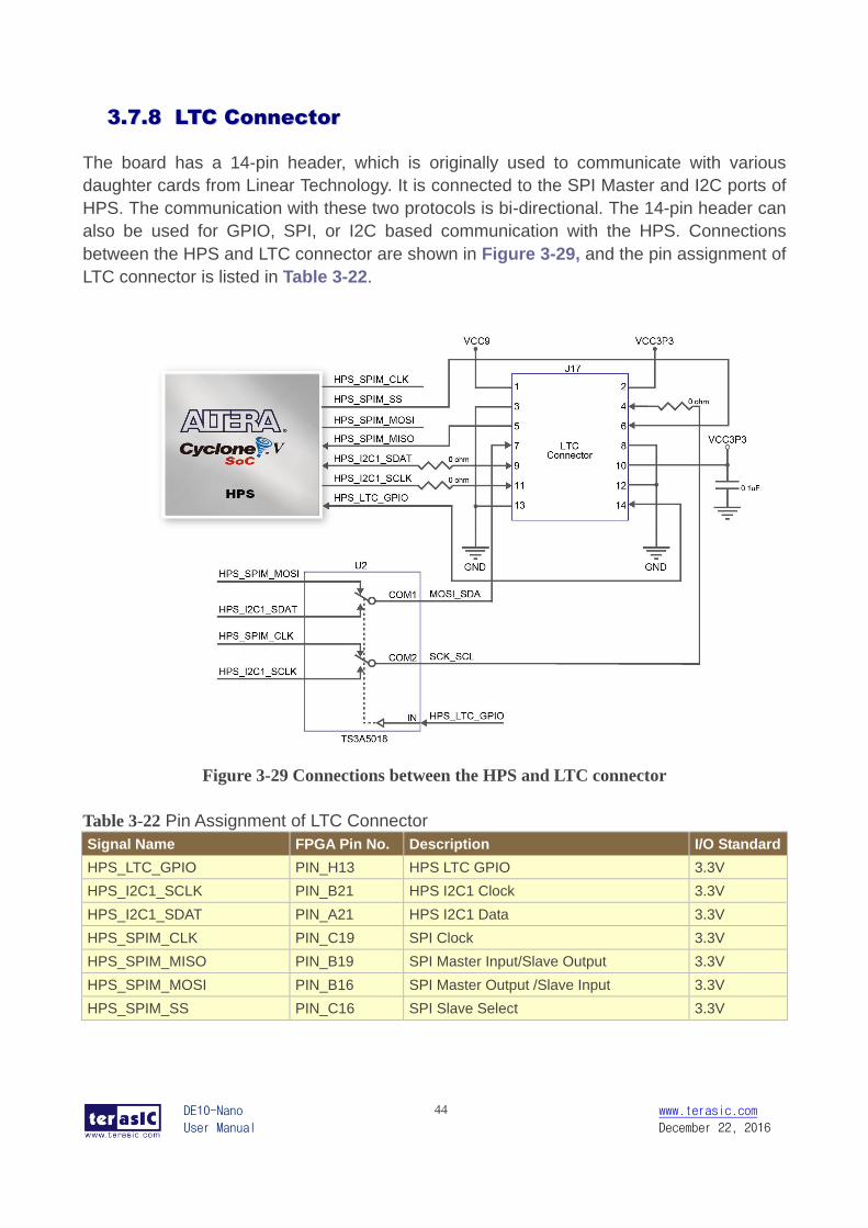
33..77..88 LLTTCC CCoonnnneeccttoorr
The board has a 14-pin header, which is originally used to communicate with various
daughter cards from Linear Technology. It is connected to the SPI Master and I2C ports of
HPS. The communication with these two protocols is bi-directional. The 14-pin header can
also be used for GPIO, SPI, or I2C based communication with the HPS. Connections
between the HPS and LTC connector are shown in Figure 3-29, and the pin assignment of
LTC connector is listed in Table 3-22.
Figure 3-29 Connections between the HPS and LTC connector
Table 3-22 Pin Assignment of LTC Connector
Signal Name FPGA Pin No. Description I/O Standard
HPS_LTC_GPIO PIN_H13 HPS LTC GPIO 3.3V
HPS_I2C1_SCLK PIN_B21 HPS I2C1 Clock 3.3V
HPS_I2C1_SDAT PIN_A21 HPS I2C1 Data 3.3V
HPS_SPIM_CLK PIN_C19 SPI Clock 3.3V
HPS_SPIM_MISO PIN_B19 SPI Master Input/Slave Output 3.3V
HPS_SPIM_MOSI PIN_B16 SPI Master Output /Slave Input 3.3V
HPS_SPIM_SS PIN_C16 SPI Slave Select 3.3V
DE10-Nano
User Manual
45 www.terasic.com
December 22, 2016
Chapter 4 DE10-Nano System
Builder
his chapter describes how users can create a custom design project with the tool
named DE10-Nano System Builder.
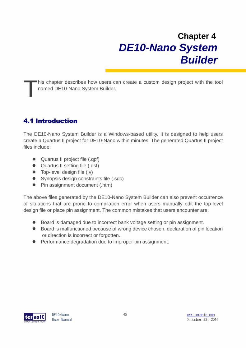
4.1 IInnttrroodduuccttiioonn
The DE10-Nano System Builder is a Windows-based utility. It is designed to help users
create a Quartus II project for DE10-Nano within minutes. The generated Quartus II project
files include:
Quartus II project file (.qpf)
Quartus II setting file (.qsf)
Top-level design file (.v)
Synopsis design constraints file (.sdc)
Pin assignment document (.htm)
The above files generated by the DE10-Nano System Builder can also prevent occurrence
of situations that are prone to compilation error when users manually edit the top-level
design file or place pin assignment. The common mistakes that users encounter are:
Board is damaged due to incorrect bank voltage setting or pin assignment.
Board is malfunctioned because of wrong device chosen, declaration of pin location
or direction is incorrect or forgotten.
Performance degradation due to improper pin assignment.
T
DE10-Nano
User Manual
46 www.terasic.com
December 22, 2016
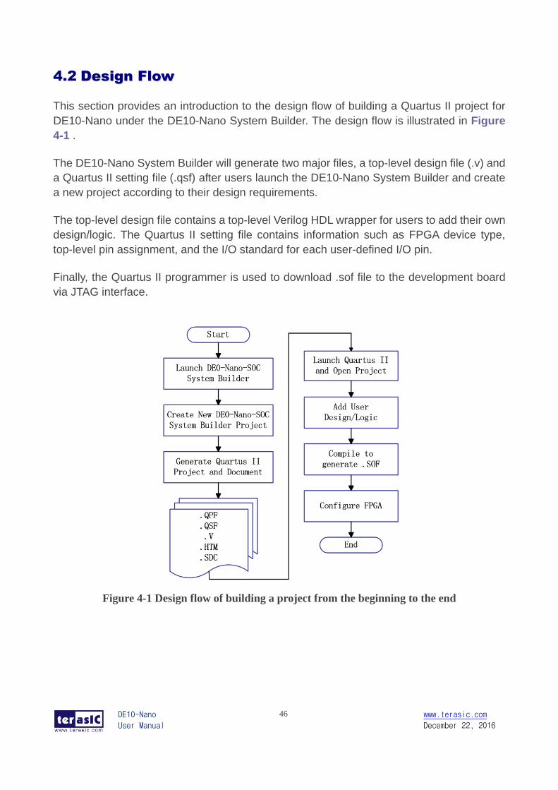
4.2 DDeessiiggnn FFllooww
This section provides an introduction to the design flow of building a Quartus II project for
DE10-Nano under the DE10-Nano System Builder. The design flow is illustrated in Figure
4-1 .
The DE10-Nano System Builder will generate two major files, a top-level design file (.v) and
a Quartus II setting file (.qsf) after users launch the DE10-Nano System Builder and create
a new project according to their design requirements.
The top-level design file contains a top-level Verilog HDL wrapper for users to add their own
design/logic. The Quartus II setting file contains information such as FPGA device type,
top-level pin assignment, and the I/O standard for each user-defined I/O pin.
Finally, the Quartus II programmer is used to download .sof file to the development board
via JTAG interface.
Figure 4-1 Design flow of building a project from the beginning to the end
DE10-Nano
User Manual
47 www.terasic.com
December 22, 2016
4.3 UUssiinngg DDEE1100--NNaannoo SSyysstteemm BBuuiillddeerr
This section provides the procedures in details on how to use the DE10-Nano System
Builder.
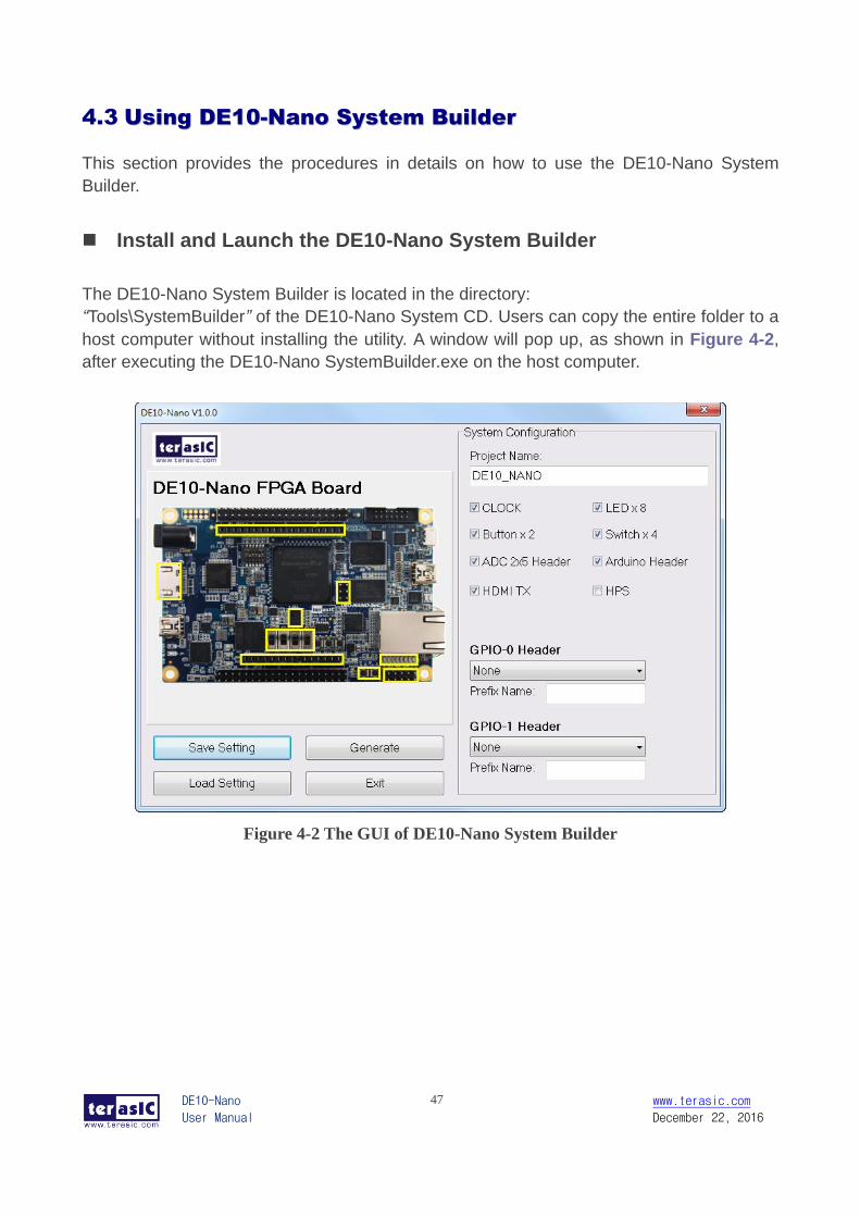
Install and Launch the DE10-Nano System Builder
The DE10-Nano System Builder is located in the directory:
“Tools\SystemBuilder” of the DE10-Nano System CD. Users can copy the entire folder to a
host computer without installing the utility. A window will pop up, as shown in Figure 4-2,
after executing the DE10-Nano SystemBuilder.exe on the host computer.
Figure 4-2 The GUI of DE10-Nano System Builder
DE10-Nano
User Manual
48 www.terasic.com
December 22, 2016
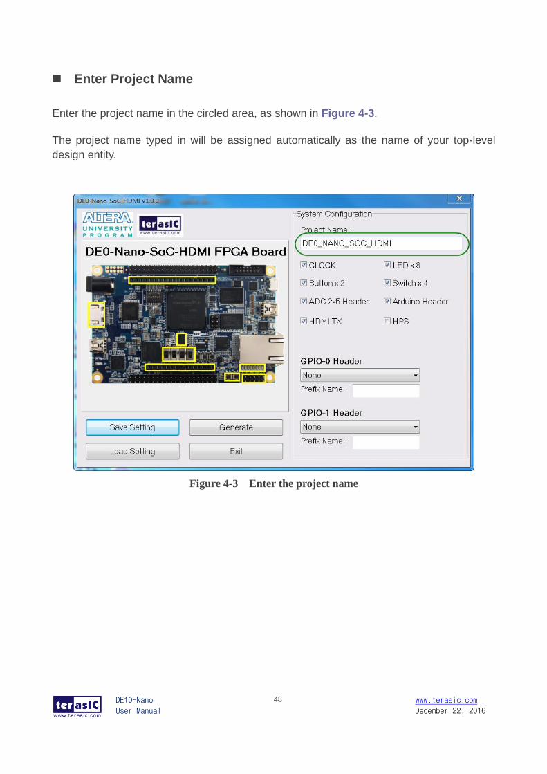
Enter Project Name
Enter the project name in the circled area, as shown in Figure 4-3.
The project name typed in will be assigned automatically as the name of your top-level
design entity.
Figure 4-3 Enter the project name
DE10-Nano
User Manual
49 www.terasic.com
December 22, 2016
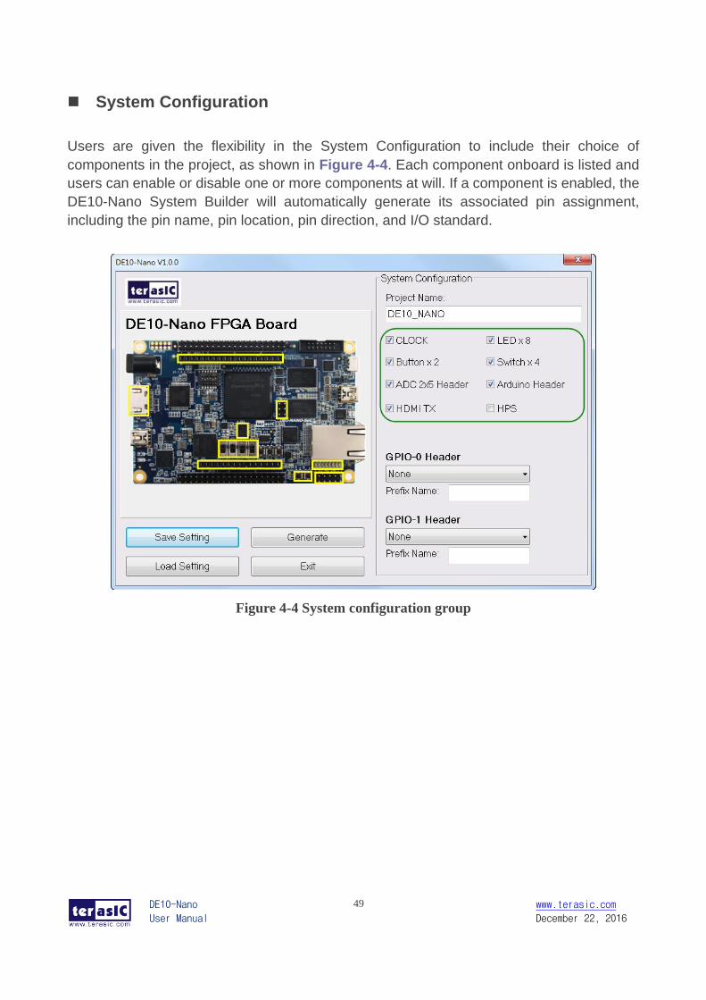
System Configuration
Users are given the flexibility in the System Configuration to include their choice of
components in the project, as shown in Figure 4-4. Each component onboard is listed and
users can enable or disable one or more components at will. If a component is enabled, the
DE10-Nano System Builder will automatically generate its associated pin assignment,
including the pin name, pin location, pin direction, and I/O standard.
Figure 4-4 System configuration group
DE10-Nano
User Manual
50 www.terasic.com
December 22, 2016
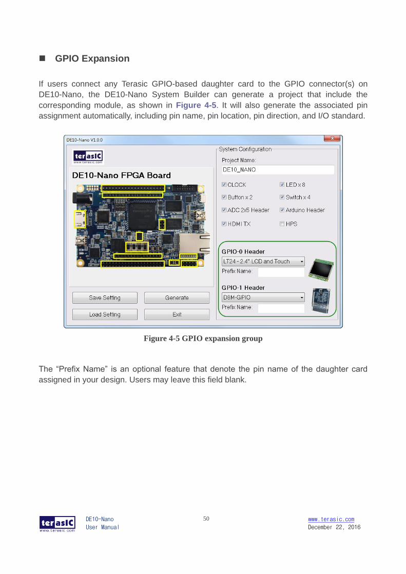
GPIO Expansion
If users connect any Terasic GPIO-based daughter card to the GPIO connector(s) on
DE10-Nano, the DE10-Nano System Builder can generate a project that include the
corresponding module, as shown in Figure 4-5. It will also generate the associated pin
assignment automatically, including pin name, pin location, pin direction, and I/O standard.
Figure 4-5 GPIO expansion group
The “Prefix Name” is an optional feature that denote the pin name of the daughter card
assigned in your design. Users may leave this field blank.
DE10-Nano
User Manual
51 www.terasic.com
December 22, 2016
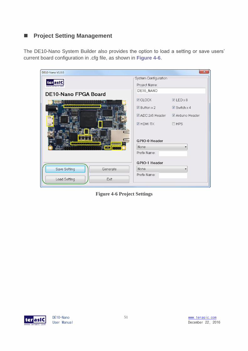
Project Setting Management
The DE10-Nano System Builder also provides the option to load a setting or save users’
current board configuration in .cfg file, as shown in Figure 4-6.
Figure 4-6 Project Settings
DE10-Nano
User Manual
52 www.terasic.com
December 22, 2016
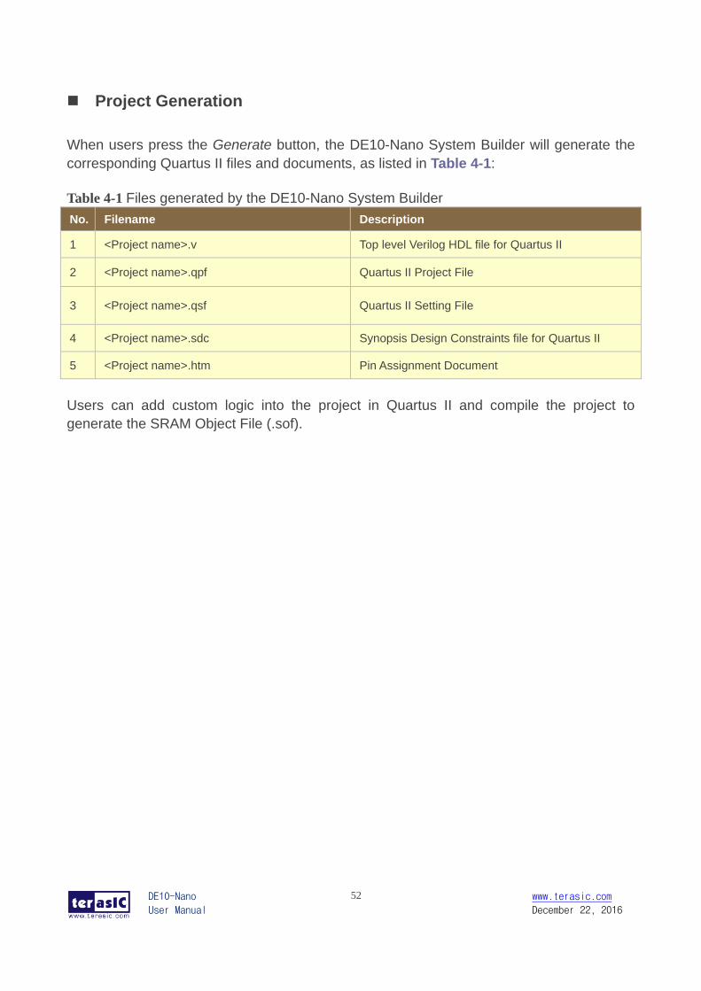
Project Generation
When users press the Generate button, the DE10-Nano System Builder will generate the
corresponding Quartus II files and documents, as listed in Table 4-1:
Table 4-1 Files generated by the DE10-Nano System Builder
No. Filename Description
1 <Project name>.v Top level Verilog HDL file for Quartus II
2 <Project name>.qpf Quartus II Project File
3 <Project name>.qsf Quartus II Setting File
4 <Project name>.sdc Synopsis Design Constraints file for Quartus II
5 <Project name>.htm Pin Assignment Document
Users can add custom logic into the project in Quartus II and compile the project to
generate the SRAM Object File (.sof).
DE10-Nano
User Manual
53 www.terasic.com
December 22, 2016
Chapter 5 Examples For FPGA
his chapter provides examples of advanced designs implemented by RTL or Qsys on
the DE10-Nano board. These reference designs cover the features of peripherals
connected to the FPGA, such as A/D Converter. All the associated files can be found
in the directory \Demonstrations\FPGA of DE10-Nano System CD.
Installation of Demonstrations
Install the demonstrations on your computer:
Copy the folder Demonstrations to a local directory of your choice. It is important to make
sure the path to your local directory contains NO space. Otherwise it will lead to error in
Nios II.
Note Quartus II v16.0 or later is required for all DE10-Nano demonstrations to support
Cyclone V SoC device.
5.1 DDEE1100--NNaannoo FFaaccttoorryy CCoonnffiigguurraattiioonn
The DE10-Nano board has a default configuration bit-stream pre-programmed, which
demonstrates some of the basic features on board. The setup required for this
demonstration and the location of its files are shown below.
Demonstration Setup, File Locations, and Instructions
Project directory: \Default
Bitstream used: DE10_NANO_Default.sof or DE10_NANO_Default.jic
Demo batch file : \Default\demo_batch\test.bat
Power on the DE10-Nano board with the USB cable connected to the USB-Blaster
II port. If necessary (that is, if the default factory configuration is not currently
stored in the EPCS device), download the bit stream to the board via JTAG
interface.
You should now be able to observe the LEDs are blinking.
T
DE10-Nano
User Manual
54 www.terasic.com
December 22, 2016
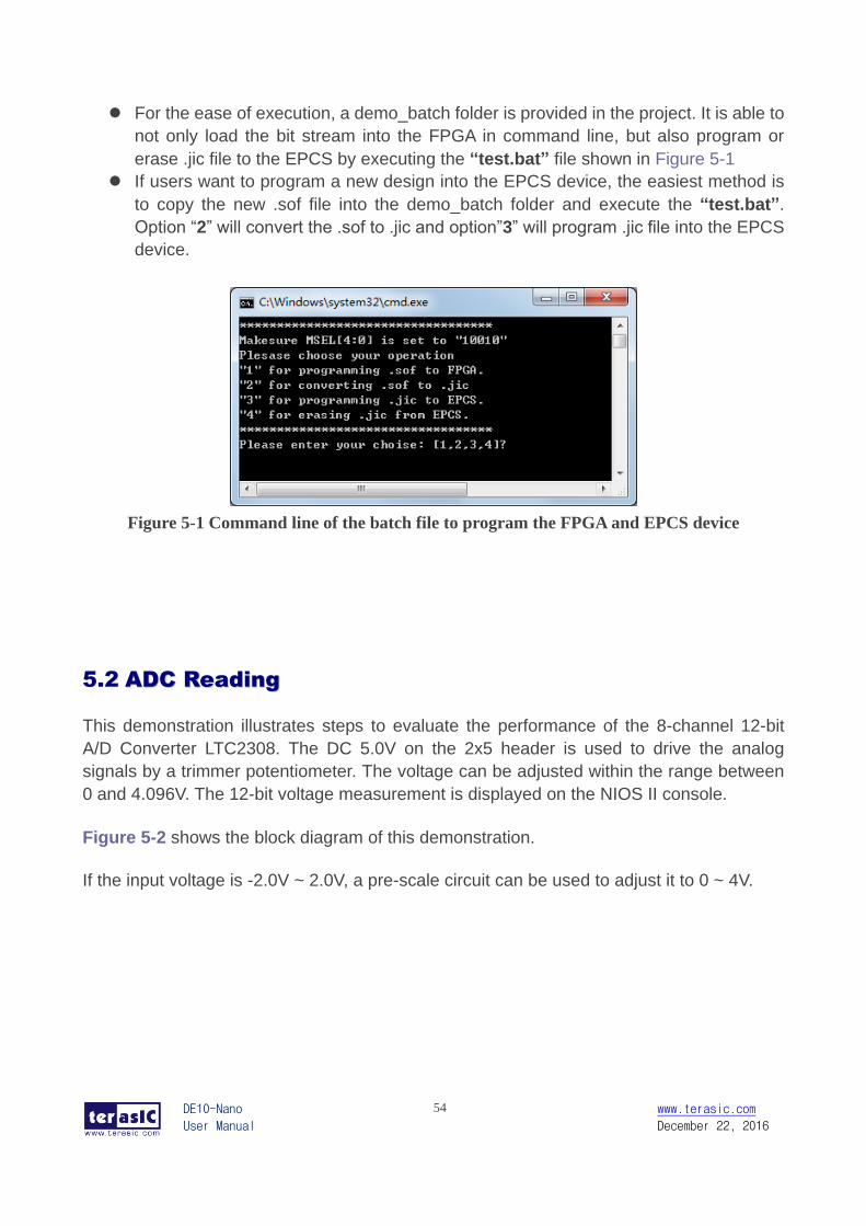
For the ease of execution, a demo_batch folder is provided in the project. It is able to
not only load the bit stream into the FPGA in command line, but also program or
erase .jic file to the EPCS by executing the “test.bat” file shown in Figure 5-1
If users want to program a new design into the EPCS device, the easiest method is
to copy the new .sof file into the demo_batch folder and execute the “test.bat”.
Option “2” will convert the .sof to .jic and option”3” will program .jic file into the EPCS
device.
Figure 5-1 Command line of the batch file to program the FPGA and EPCS device
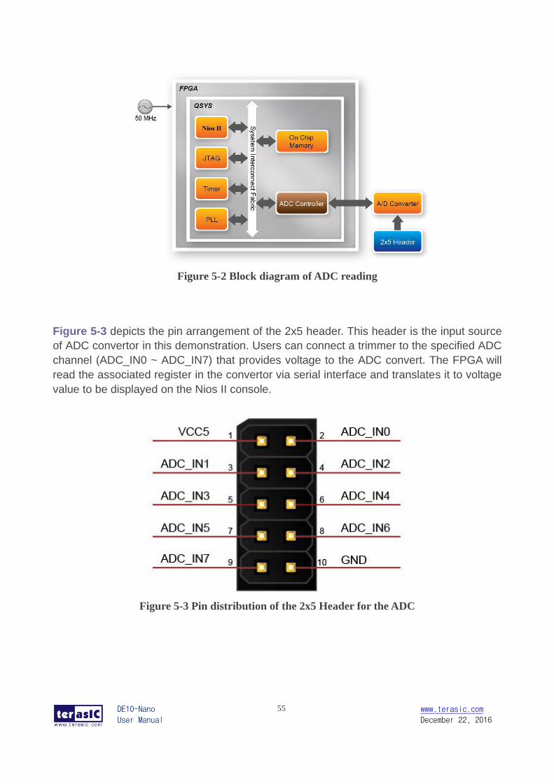
5.2 AADDCC RReeaaddiinngg
This demonstration illustrates steps to evaluate the performance of the 8-channel 12-bit
A/D Converter LTC2308. The DC 5.0V on the 2x5 header is used to drive the analog
signals by a trimmer potentiometer. The voltage can be adjusted within the range between
0 and 4.096V. The 12-bit voltage measurement is displayed on the NIOS II console.
Figure 5-2 shows the block diagram of this demonstration.
If the input voltage is -2.0V ~ 2.0V, a pre-scale circuit can be used to adjust it to 0 ~ 4V.
DE10-Nano
User Manual
55 www.terasic.com
December 22, 2016
Figure 5-2 Block diagram of ADC reading
Figure 5-3 depicts the pin arrangement of the 2x5 header. This header is the input source
of ADC convertor in this demonstration. Users can connect a trimmer to the specified ADC
channel (ADC_IN0 ~ ADC_IN7) that provides voltage to the ADC convert. The FPGA will
read the associated register in the convertor via serial interface and translates it to voltage
value to be displayed on the Nios II console.
Figure 5-3 Pin distribution of the 2x5 Header for the ADC
DE10-Nano
User Manual
56 www.terasic.com
December 22, 2016
System Requirements
The following items are required for this demonstration.
DE10-Nano board x1
Trimmer Potentiometer x1
Wire Strip x3
Demonstration File Locations
Hardware project directory: \ADC
Bitstream used: DE10_NANO_ADC.sof
Software project directory: \ADC\software
Nios II program: DE10_NANO_ADC.elf
Demo batch file : \ADC\demo_batch\test.bat
Demonstration Setup and Instructions
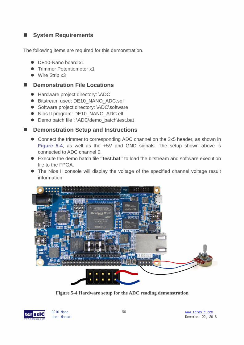
Connect the trimmer to corresponding ADC channel on the 2x5 header, as shown in
Figure 5-4, as well as the +5V and GND signals. The setup shown above is
connected to ADC channel 0.
Execute the demo batch file “test.bat” to load the bitstream and software execution
file to the FPGA.
The Nios II console will display the voltage of the specified channel voltage result
information
Figure 5-4 Hardware setup for the ADC reading demonstration
DE10-Nano
User Manual
57 www.terasic.com
December 22, 2016
5.3 HHDDMMII TTXX
This section gives instructions to program the HDMI transmitter to generate video pattern
and audio source. The entire reference is composed into three parts: video design, audio
design, and I2C design. A set of built-in video patterns and audio serial data will be sent to
the HDMI transmitter to drive the HDMI display with speaker. Users can hear the beeping
sound from the speaker when SW0 is set to 1 on the DE10-Nano board. The resolution can
be switched by pressing KEY1.
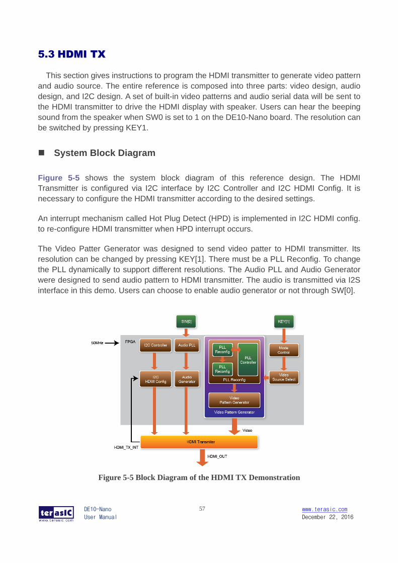
System Block Diagram
Figure 5-5 shows the system block diagram of this reference design. The HDMI
Transmitter is configured via I2C interface by I2C Controller and I2C HDMI Config. It is
necessary to configure the HDMI transmitter according to the desired settings.
An interrupt mechanism called Hot Plug Detect (HPD) is implemented in I2C HDMI config.
to re-configure HDMI transmitter when HPD interrupt occurs.
The Video Patter Generator was designed to send video patter to HDMI transmitter. Its
resolution can be changed by pressing KEY[1]. There must be a PLL Reconfig. To change
the PLL dynamically to support different resolutions. The Audio PLL and Audio Generator
were designed to send audio pattern to HDMI transmitter. The audio is transmitted via I2S
interface in this demo. Users can choose to enable audio generator or not through SW[0].
Figure 5-5 Block Diagram of the HDMI TX Demonstration
DE10-Nano
User Manual
58 www.terasic.com
December 22, 2016
Register of HDMI Transmitter (ADV7513)
Users can save lots of developing time by paying attention to the settings of video format
and audio frequency in register at address 0x15 and the format of register at address 0xAF
prior to the development of HDMI transmitter. This demo uses 48KHz sampling rate and the
video format is 24-bit RGB 4:4:4. For more details, please refer to the document
ADV7513_Programming_Guide_R0.pdf.
Audio Generator
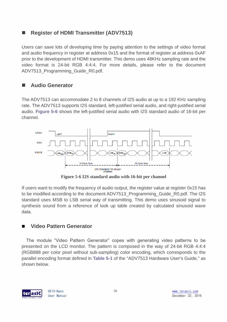
The ADV7513 can accommodate 2 to 8 channels of I2S audio at up to a 192 KHz sampling
rate. The ADV7513 supports I2S standard, left-justified serial audio, and right-justified serial
audio. Figure 5-6 shows the left-justified serial audio with I2S standard audio of 16-bit per
channel.
Figure 5-6 I2S standard audio with 16-bit per channel
If users want to modify the frequency of audio output, the register value at register 0x15 has
to be modified according to the document ADV7513_Programming_Guide_R0.pdf. The I2S
standard uses MSB to LSB serial way of transmitting. This demo uses sinusoid signal to
synthesis sound from a reference of look up table created by calculated sinusoid wave
data.
Video Pattern Generator
The module “Video Pattern Generator” copes with generating video patterns to be
presented on the LCD monitor. The pattern is composed in the way of 24-bit RGB 4:4:4
(RGB888 per color pixel without sub-sampling) color encoding, which corresponds to the
parallel encoding format defined in Table 5-1 of the "ADV7513 Hardware User's Guide," as
shown below.
DE10-Nano
User Manual
59 www.terasic.com
December 22, 2016
Table 5-1 Display modes of the HDMI TX demonstration
A set of display modes is implemented for presenting the generated video patterns. The
module “Video Source Selector” controls the selection of current video timing among
built-in display modes listed in Table 5-2. The module "Mode Control" allows users to
switch current display mode alternatively via KEY1.
Table 5-2 Built-in display modes for the HDMI TX demonstration
Demonstration File Locations
Hardware project directory: \HDMI_TX
Bitstream used: DE10_Nano_HDMI_TX.sof
Demo batch file : \HDMI_TX\demo_batch\test.bat
Demonstration Setup and Instructions
Please make sure both Quartus II and USB-Blaster II driver are installed on the host
PC.
Connect the DE10-Nano board to the LCD monitor through a HDMI cable.
Power on the DE10-Nano board
Launch the "test.bat" batch file from the "\HDMI_TX\demo_batch" folder. After the
programming and configuration are successful, the screen should look like the one
shown in Figure 5-7 .
Pixel Data [23:0]
17 16 15 14 13 12 11 10 9 8 7 6 5 4 3 2 1 0
R[7:0] G[7:0] B[7:0]
Pattern ID Video Format PCLK (MHZ)
0 640x480@60P 25
1 720x480@60P 27
2 1024x768@60P 65
3 1280x1024@60P 108
4 1920x1080@60P 148.5
DE10-Nano
User Manual
60 www.terasic.com
December 22, 2016
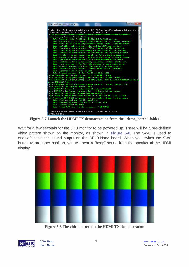
Figure 5-7 Launch the HDMI TX demonstration from the "demo_batch" folder
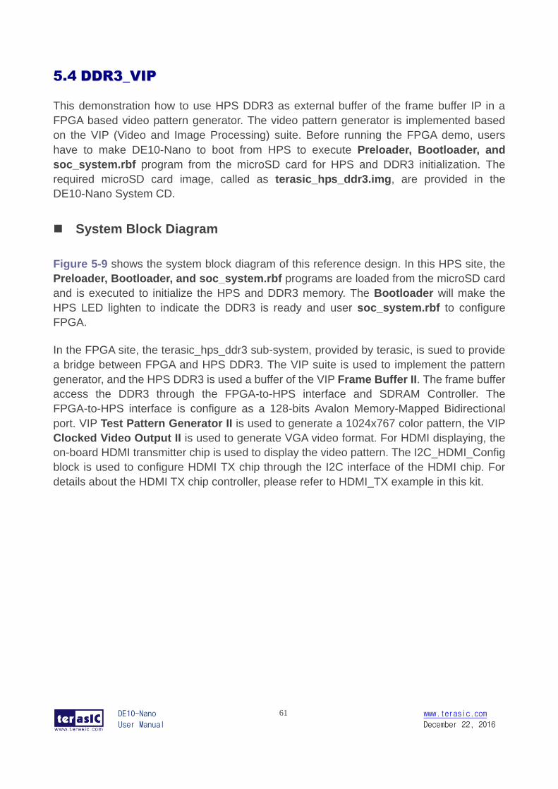
Wait for a few seconds for the LCD monitor to be powered up. There will be a pre-defined
video pattern shown on the monitor, as shown in Figure 5-8. The SW0 is used to
enable/disable the sound output on the DE10-Nano board. When you switch the SW0
button to an upper position, you will hear a "beep" sound from the speaker of the HDMI
display.
Figure 5-8 The video pattern in the HDMI TX demonstration
DE10-Nano
User Manual
61 www.terasic.com
December 22, 2016
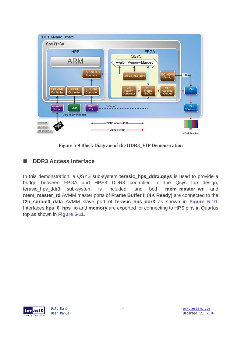
5.4 DDDDRR33__VVIIPP
This demonstration how to use HPS DDR3 as external buffer of the frame buffer IP in a
FPGA based video pattern generator. The video pattern generator is implemented based
on the VIP (Video and Image Processing) suite. Before running the FPGA demo, users
have to make DE10-Nano to boot from HPS to execute Preloader, Bootloader, and
soc_system.rbf program from the microSD card for HPS and DDR3 initialization. The
required microSD card image, called as terasic_hps_ddr3.img, are provided in the
DE10-Nano System CD.
System Block Diagram
Figure 5-9 shows the system block diagram of this reference design. In this HPS site, the
Preloader, Bootloader, and soc_system.rbf programs are loaded from the microSD card
and is executed to initialize the HPS and DDR3 memory. The Bootloader will make the
HPS LED lighten to indicate the DDR3 is ready and user soc_system.rbf to configure
FPGA.
In the FPGA site, the terasic_hps_ddr3 sub-system, provided by terasic, is sued to provide
a bridge between FPGA and HPS DDR3. The VIP suite is used to implement the pattern
generator, and the HPS DDR3 is used a buffer of the VIP Frame Buffer II. The frame buffer
access the DDR3 through the FPGA-to-HPS interface and SDRAM Controller. The
FPGA-to-HPS interface is configure as a 128-bits Avalon Memory-Mapped Bidirectional
port. VIP Test Pattern Generator II is used to generate a 1024x767 color pattern, the VIP
Clocked Video Output II is used to generate VGA video format. For HDMI displaying, the
on-board HDMI transmitter chip is used to display the video pattern. The I2C_HDMI_Config
block is used to configure HDMI TX chip through the I2C interface of the HDMI chip. For
details about the HDMI TX chip controller, please refer to HDMI_TX example in this kit.
DE10-Nano
User Manual
62 www.terasic.com
December 22, 2016
Figure 5-9 Block Diagram of the DDR3_VIP Demonstration
DDR3 Access Interface
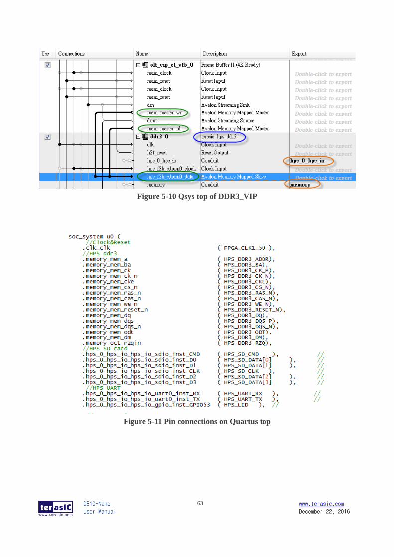
In this demonstration, a QSYS sub-system terasic_hps_ddr3.qsys is used to provide a
bridge between FPGA and HPS3 DDR3 controller. In the Qsys top design,
terasic_hps_ddr3 sub-system is included, and both mem_master_wr and
mem_master_rd AVMM master ports of Frame Buffer II (4K Ready) are connected to the
f2h_sdram0_data AVMM slave port of terasic_hps_ddr3 as shown in Figure 5-10.
Interfaces hps_0_hps_io and memory are exported for connecting to HPS pins in Quartus
top as shown in Figure 5-11.
DE10-Nano
User Manual
63 www.terasic.com
December 22, 2016
Figure 5-10 Qsys top of DDR3_VIP
Figure 5-11 Pin connections on Quartus top
DE10-Nano
User Manual
64 www.terasic.com
December 22, 2016
FPGA configure from HPS
Beside configure FGPA through the usb-blaster JTAG interface. The FPGA also can be
configured by Bootloader in the microSD card. When DE10-Nano is booted from HPS, the
Bootloader will configure the FPGA by the configuration file soc_system.rbf which is also
provided in the microSD card. The soc_system.rbf file can be generated from a .sof by
applying a batch file sof_to_rbf.bat. The batched file is provided by terasic, and is located
in the VIP_DDR3 folder. The batch call utility quarthps_cpf.exe to translate DDR3_VIP.sof
to soc_system.rbf.
Before copy this soc_system.rbf into the MicroSD card, that, please make sure the
microSD card are programmed with the Linux Image file terasic_hsp_ddr3_init.img located
at
CD\Demonstration\FPGA\SdcardImage\terasic_hps_ddr3.img
For details about how to program the terasic_hps_ddr3.img into the microSD card, Please
refer to Getting_Started_Guide.pdf document in this kit.
Here are the procedure to generate and copy the soc_system.rbf into the microSD card:
Make sure the DDR3_VIP.sof file is up to date on the DDR3_VIP project folder
Execute sof_to_rbf.bat to generate soc_system.rbf
Make sure the microSD card had programmed to contains the Linux image
erasic_hps_ddr3.img
Insert the MicroSD card into your host PC
Copy soc_system.rbf to root folder of the microSD card. (Overwrite soc_system.rbf
if there is old one existed)
Demonstration File Locations
The Quartus project information is shown below:
FPGA Quartus project location: CD\Demonstrations\FPGA\DDR3_VIP
Demo batch file location : CD\Demonstrations\FPGA\DDR3_VIP\demo_batch
Bitstream File Name: DDR3_VIP.sof
RBF Filename: soc_system.rbf
DE10-Nano
User Manual
65 www.terasic.com
December 22, 2016
The location of the Linux image to program microSD is specified below. Please refer to
Getting_Started_Guide.pdf about how to program the Linux image into a microSD card by
using Win32DiskImager.exe.
CD\Demonstrations\FPGA\SdcardImage\ terasic_hps_ddr3.img
Demonstration Setup and Instructions by SOF File
Please following below instruction to configure FPGA with .sof file through the usb-blaster
JTAG interface to performance the demonstration.
Make sure both Quartus II and USB-Blaster II driver are installed on the host PC.
Connect the DE10-Nano board to the LCD monitor through a HDMI cable.
Program terasic_hps_ddr3.img into a microSD card.
Insert the microSD card into the DE10-Nano board.
Make sure the MSEL[4:0] is set to 01010.
Connect a mini-USB cable to UB2 port of DE10-Nano and the host PC.
Power on the DE10-Nano board
Wait the HPS LED0 is lighted. This indicate the DDR3 is ready.
Launch the "test.bat" batch file from the "\DDR3_VIP\demo_batch" folder. After
the programming and configuration are successful, the screen should look like the
one shown in Figure 5-12 .
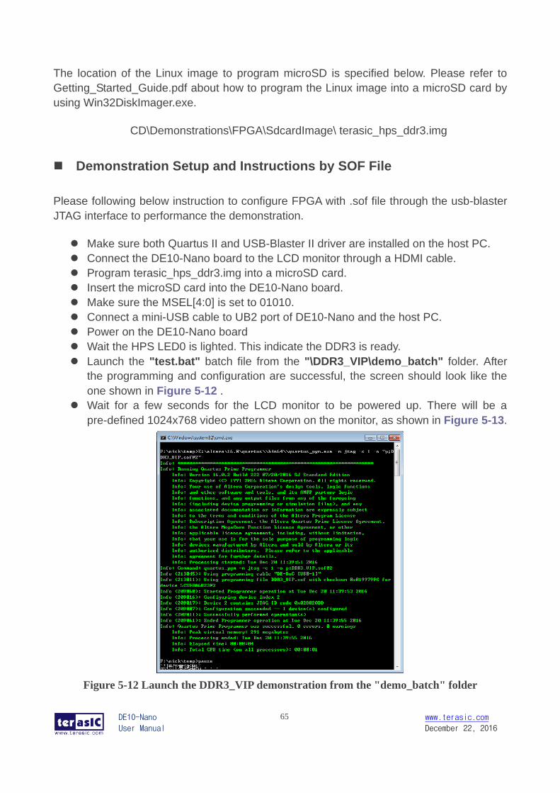
Wait for a few seconds for the LCD monitor to be powered up. There will be a
pre-defined 1024x768 video pattern shown on the monitor, as shown in Figure 5-13.
Figure 5-12 Launch the DDR3_VIP demonstration from the "demo_batch" folder
DE10-Nano
User Manual
66 www.terasic.com
December 22, 2016
Figure 5-13 The video pattern in the DDR3_VIP demonstration
Demonstration Setup and Instructions by RBF File
Please following instructions below to configure FPGA with soc_system.rbf file to
performance the demonstration. In this demonstration case, FPGA is configured by
Bootloader which read the configuration file soc_system.rbf from the microSD card. In
this demonstration setup, no USB cable is required.
Connect the DE10-Nano board to the LCD monitor through a HDMI cable.
Programming terasic_hps_ddr3.img into a microSD card.
Copy the RBF file soc_system.rbf into the microSD card.
Insert the microSD card into the DE10-Nano board.
Make sure the MSEL[4:0] is set to 01010.
Power on the DE10-Nano board
Wait for a few seconds for the LCD monitor to be powered up. There will be a
1024x768 video pattern shown on the monitor.
DE10-Nano
User Manual
67 www.terasic.com
December 22, 2016
Chapter 6 Examples for
HPS SoC
his chapter provides several C-code examples based on the Intel SoC Linux built by
Yocto project. These examples demonstrate major features of peripherals connected
to HPS interface on DE10-Nano board such as users LED/KEY, I2C interfaced
G-sensor. All the associated files can be found in the directory Demonstrations/SOC of the
DE10-Nano System CD. Please refer to Chapter 5 "Running Linux on the DE10-Nano
board" from the DE10-Nano_Getting_Started_Guide.pdf to run Linux on DE10-Nano
board.
Installation of the Demonstrations
To install the demonstrations on the host computer:
Copy the directory Demonstrations into a local directory of your choice. SoC EDS V16.0 is
required for users to compile the c-code project.
6.1 HHeelllloo PPrrooggrraamm
This demonstration shows how to develop first HPS program with SoC EDS tool. Please
refer to My_First_HPS.pdf from the system CD for more details.
The major procedures to develop and build HPS project are:
Install SoC EDS on the host PC.
Create program .c/.h files with a generic text editor
Create a "Makefile" with a generic text editor
Build the project under SoC EDS
T
DE10-Nano
User Manual
68 www.terasic.com
December 22, 2016
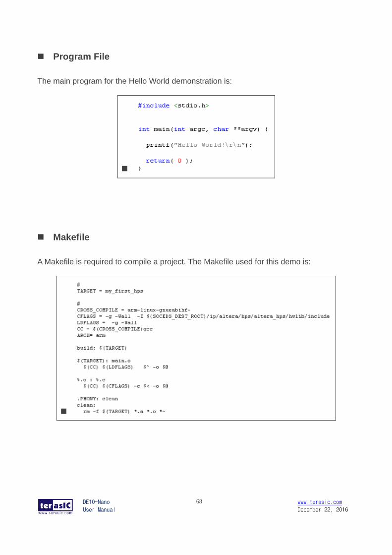
Program File
The main program for the Hello World demonstration is:
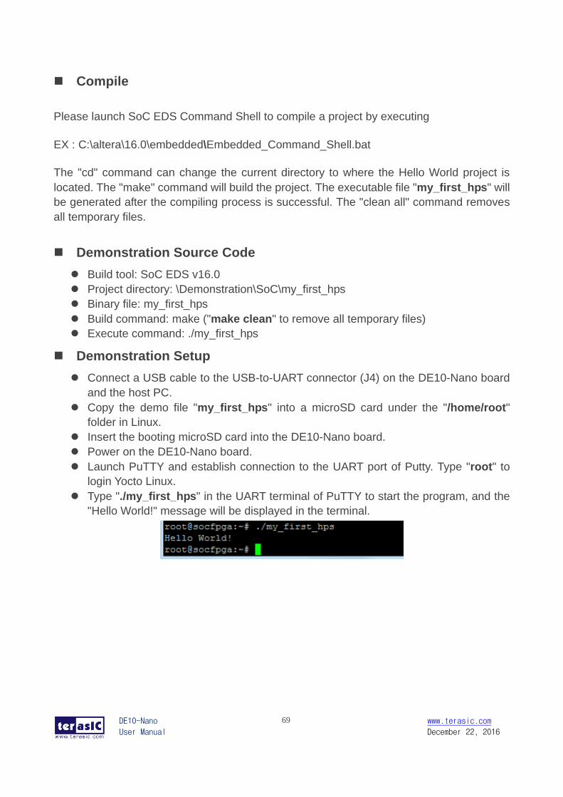
Makefile
A Makefile is required to compile a project. The Makefile used for this demo is:
DE10-Nano
User Manual
69 www.terasic.com
December 22, 2016
Compile
Please launch SoC EDS Command Shell to compile a project by executing
EX : C:\altera\16.0\embedded\Embedded_Command_Shell.bat
The "cd" command can change the current directory to where the Hello World project is
located. The "make" command will build the project. The executable file "my_first_hps" will
be generated after the compiling process is successful. The "clean all" command removes
all temporary files.
Demonstration Source Code
Build tool: SoC EDS v16.0
Project directory: \Demonstration\SoC\my_first_hps
Binary file: my_first_hps
Build command: make ("make clean" to remove all temporary files)
Execute command: ./my_first_hps
Demonstration Setup
Connect a USB cable to the USB-to-UART connector (J4) on the DE10-Nano board
and the host PC.
Copy the demo file "my_first_hps" into a microSD card under the "/home/root"
folder in Linux.
Insert the booting microSD card into the DE10-Nano board.
Power on the DE10-Nano board.
Launch PuTTY and establish connection to the UART port of Putty. Type "root" to
login Yocto Linux.
Type "./my_first_hps" in the UART terminal of PuTTY to start the program, and the
"Hello World!" message will be displayed in the terminal.
DE10-Nano
User Manual
70 www.terasic.com
December 22, 2016
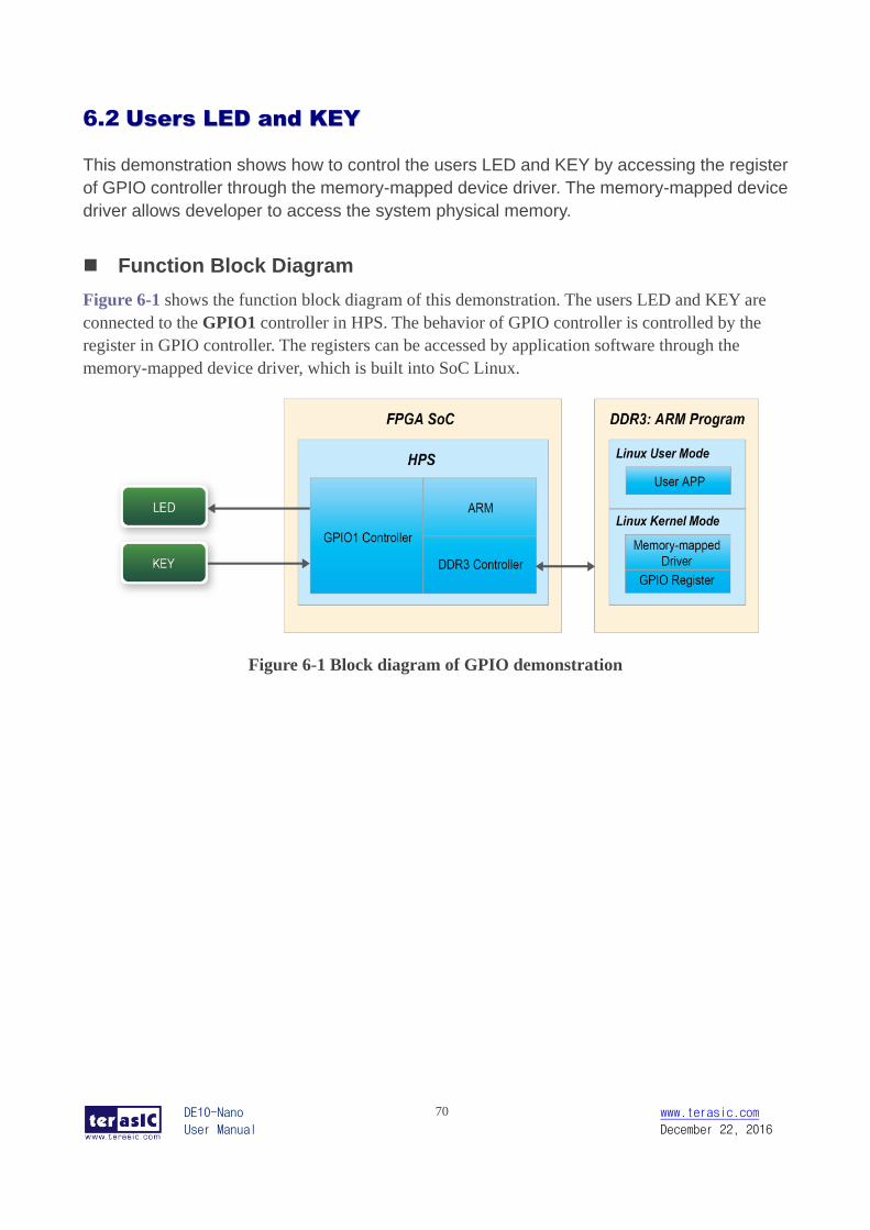
6.2 UUsseerrss LLEEDD aanndd KKEEYY
This demonstration shows how to control the users LED and KEY by accessing the register
of GPIO controller through the memory-mapped device driver. The memory-mapped device
driver allows developer to access the system physical memory.
Function Block Diagram
Figure 6-1 shows the function block diagram of this demonstration. The users LED and KEY are
connected to the GPIO1 controller in HPS. The behavior of GPIO controller is controlled by the
register in GPIO controller. The registers can be accessed by application software through the
memory-mapped device driver, which is built into SoC Linux.
Figure 6-1 Block diagram of GPIO demonstration
DE10-Nano
User Manual
71 www.terasic.com
December 22, 2016
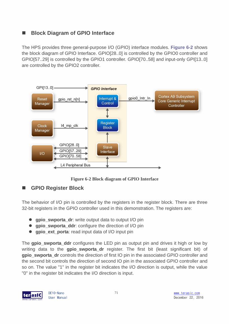
Block Diagram of GPIO Interface
The HPS provides three general-purpose I/O (GPIO) interface modules. Figure 6-2 shows
the block diagram of GPIO Interface. GPIO[28..0] is controlled by the GPIO0 controller and
GPIO[57..29] is controlled by the GPIO1 controller. GPIO[70..58] and input-only GPI[13..0]
are controlled by the GPIO2 controller.
Figure 6-2 Block diagram of GPIO Interface
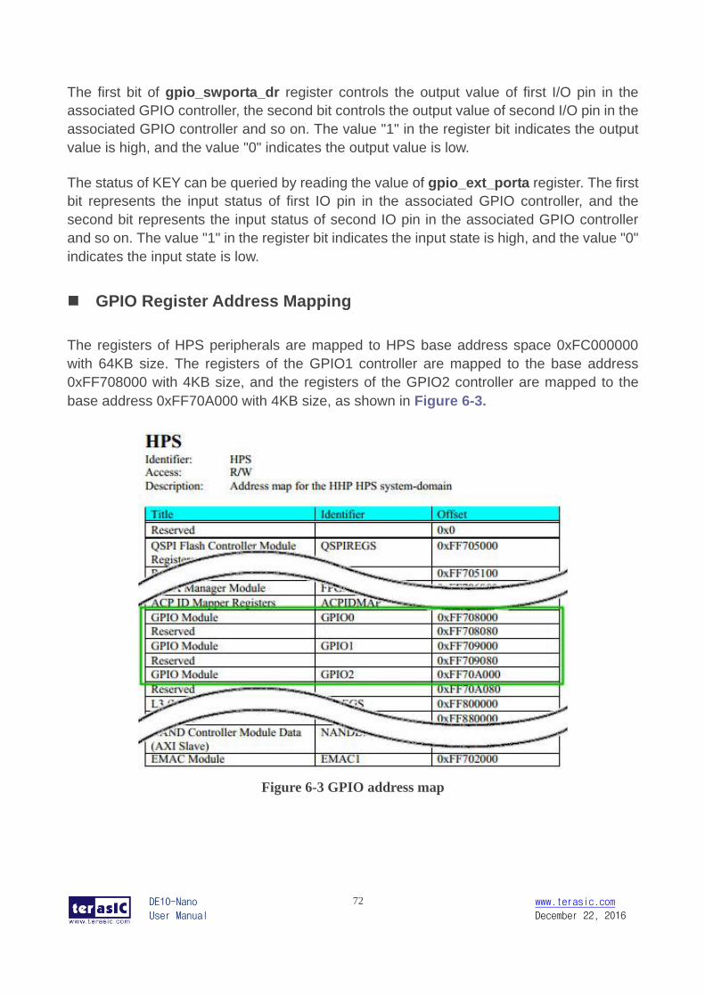
GPIO Register Block
The behavior of I/O pin is controlled by the registers in the register block. There are three
32-bit registers in the GPIO controller used in this demonstration. The registers are:
gpio_swporta_dr: write output data to output I/O pin
gpio_swporta_ddr: configure the direction of I/O pin
gpio_ext_porta: read input data of I/O input pin
The gpio_swporta_ddr configures the LED pin as output pin and drives it high or low by
writing data to the gpio_swporta_dr register. The first bit (least significant bit) of
gpio_swporta_dr controls the direction of first IO pin in the associated GPIO controller and
the second bit controls the direction of second IO pin in the associated GPIO controller and
so on. The value "1" in the register bit indicates the I/O direction is output, while the value
"0" in the register bit indicates the I/O direction is input.
DE10-Nano
User Manual
72 www.terasic.com
December 22, 2016
The first bit of gpio_swporta_dr register controls the output value of first I/O pin in the
associated GPIO controller, the second bit controls the output value of second I/O pin in the
associated GPIO controller and so on. The value "1" in the register bit indicates the output
value is high, and the value "0" indicates the output value is low.
The status of KEY can be queried by reading the value of gpio_ext_porta register. The first
bit represents the input status of first IO pin in the associated GPIO controller, and the
second bit represents the input status of second IO pin in the associated GPIO controller
and so on. The value "1" in the register bit indicates the input state is high, and the value "0"
indicates the input state is low.
GPIO Register Address Mapping
The registers of HPS peripherals are mapped to HPS base address space 0xFC000000
with 64KB size. The registers of the GPIO1 controller are mapped to the base address
0xFF708000 with 4KB size, and the registers of the GPIO2 controller are mapped to the
base address 0xFF70A000 with 4KB size, as shown in Figure 6-3.
Figure 6-3 GPIO address map
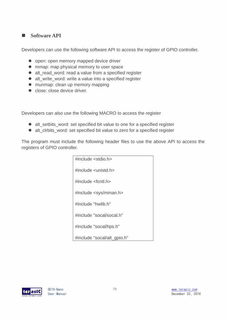
DE10-Nano
User Manual
73 www.terasic.com
December 22, 2016
Software API
Developers can use the following software API to access the register of GPIO controller.
open: open memory mapped device driver
mmap: map physical memory to user space
alt_read_word: read a value from a specified register
alt_write_word: write a value into a specified register
munmap: clean up memory mapping
close: close device driver.
Developers can also use the following MACRO to access the register
alt_setbits_word: set specified bit value to one for a specified register
alt_clrbits_word: set specified bit value to zero for a specified register
The program must include the following header files to use the above API to access the
registers of GPIO controller.
#include <stdio.h>
#include <unistd.h>
#include <fcntl.h>
#include <sys/mman.h>
#include "hwlib.h"
#include "socal/socal.h"
#include "socal/hps.h"
#include "socal/alt_gpio.h"
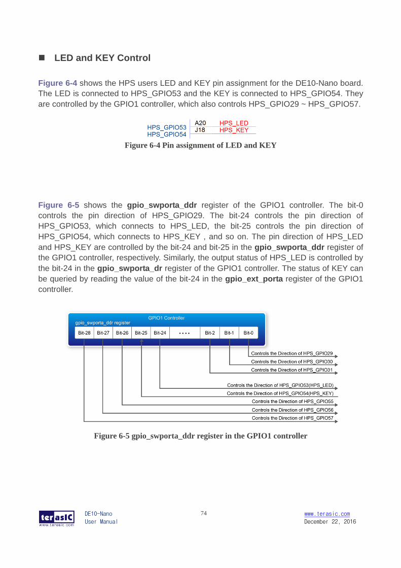
DE10-Nano
User Manual
74 www.terasic.com
December 22, 2016
LED and KEY Control
Figure 6-4 shows the HPS users LED and KEY pin assignment for the DE10-Nano board.
The LED is connected to HPS_GPIO53 and the KEY is connected to HPS_GPIO54. They
are controlled by the GPIO1 controller, which also controls HPS_GPIO29 ~ HPS_GPIO57.
Figure 6-4 Pin assignment of LED and KEY
Figure 6-5 shows the gpio_swporta_ddr register of the GPIO1 controller. The bit-0
controls the pin direction of HPS_GPIO29. The bit-24 controls the pin direction of
HPS_GPIO53, which connects to HPS_LED, the bit-25 controls the pin direction of
HPS_GPIO54, which connects to HPS_KEY , and so on. The pin direction of HPS_LED
and HPS_KEY are controlled by the bit-24 and bit-25 in the gpio_swporta_ddr register of
the GPIO1 controller, respectively. Similarly, the output status of HPS_LED is controlled by
the bit-24 in the gpio_swporta_dr register of the GPIO1 controller. The status of KEY can
be queried by reading the value of the bit-24 in the gpio_ext_porta register of the GPIO1
controller.
Figure 6-5 gpio_swporta_ddr register in the GPIO1 controller
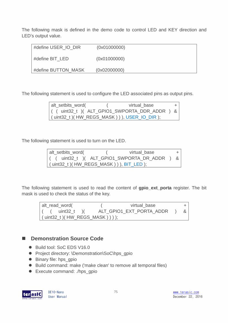
DE10-Nano
User Manual
75 www.terasic.com
December 22, 2016
The following mask is defined in the demo code to control LED and KEY direction and
LED’s output value.
#define USER_IO_DIR (0x01000000)
#define BIT_LED (0x01000000)
#define BUTTON_MASK (0x02000000)
The following statement is used to configure the LED associated pins as output pins.
alt_setbits_word( ( virtual_base +
( ( uint32_t )( ALT_GPIO1_SWPORTA_DDR_ADDR ) &
( uint32_t )( HW_REGS_MASK ) ) ), USER_IO_DIR );
The following statement is used to turn on the LED.
alt_setbits_word( ( virtual_base +
( ( uint32_t )( ALT_GPIO1_SWPORTA_DR_ADDR ) &
( uint32_t )( HW_REGS_MASK ) ) ), BIT_LED );
The following statement is used to read the content of gpio_ext_porta register. The bit
mask is used to check the status of the key.
alt_read_word( ( virtual_base +
( ( uint32_t )( ALT_GPIO1_EXT_PORTA_ADDR ) &
( uint32_t )( HW_REGS_MASK ) ) ) );
Demonstration Source Code
Build tool: SoC EDS V16.0
Project directory: \Demonstration\SoC\hps_gpio
Binary file: hps_gpio
Build command: make ('make clean' to remove all temporal files)
Execute command: ./hps_gpio
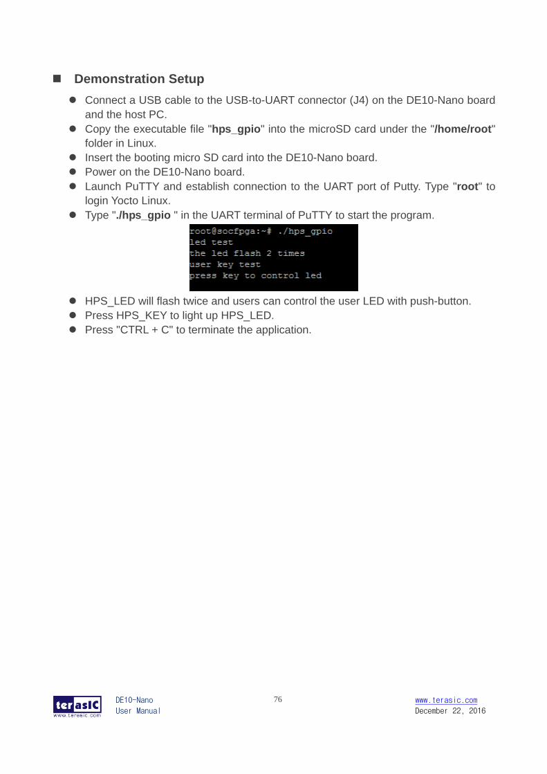
DE10-Nano
User Manual
76 www.terasic.com
December 22, 2016
Demonstration Setup
Connect a USB cable to the USB-to-UART connector (J4) on the DE10-Nano board
and the host PC.
Copy the executable file "hps_gpio" into the microSD card under the "/home/root"
folder in Linux.
Insert the booting micro SD card into the DE10-Nano board.
Power on the DE10-Nano board.
Launch PuTTY and establish connection to the UART port of Putty. Type "root" to
login Yocto Linux.
Type "./hps_gpio " in the UART terminal of PuTTY to start the program.
HPS_LED will flash twice and users can control the user LED with push-button.
Press HPS_KEY to light up HPS_LED.
Press "CTRL + C" to terminate the application.
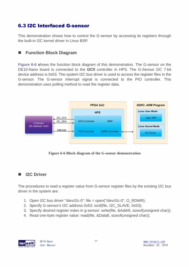
DE10-Nano
User Manual
77 www.terasic.com
December 22, 2016
6.3 II22CC IInntteerrffaacceedd GG--sseennssoorr
This demonstration shows how to control the G-sensor by accessing its registers through
the built-in I2C kernel driver in Linux BSP.
Function Block Diagram
Figure 6-6 shows the function block diagram of this demonstration. The G-sensor on the
DE10-Nano board is connected to the I2C0 controller in HPS. The G-Sensor I2C 7-bit
device address is 0x53. The system I2C bus driver is used to access the register files in the
G-sensor. The G-sensor interrupt signal is connected to the PIO controller. This
demonstration uses polling method to read the register data.
Figure 6-6 Block diagram of the G-sensor demonstration
I2C Driver
The procedures to read a register value from G-sensor register files by the existing I2C bus
driver in the system are:
1. Open I2C bus driver "/dev/i2c-0": file = open("/dev/i2c-0", O_RDWR);
2. Specify G-sensor's I2C address 0x53: ioctl(file, I2C_SLAVE, 0x53);
3. Specify desired register index in g-sensor: write(file, &Addr8, sizeof(unsigned char));
4. Read one-byte register value: read(file, &Data8, sizeof(unsigned char));
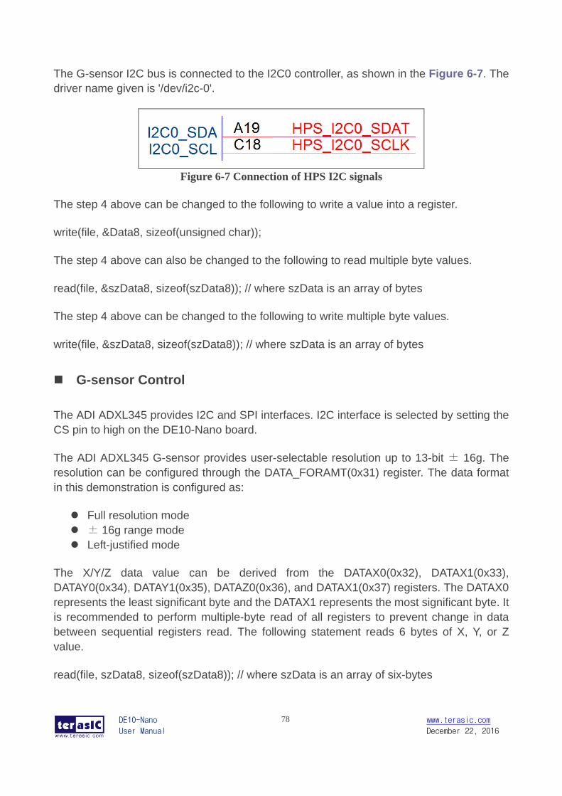
DE10-Nano
User Manual
78 www.terasic.com
December 22, 2016
The G-sensor I2C bus is connected to the I2C0 controller, as shown in the Figure 6-7. The
driver name given is '/dev/i2c-0'.
Figure 6-7 Connection of HPS I2C signals
The step 4 above can be changed to the following to write a value into a register.
write(file, &Data8, sizeof(unsigned char));
The step 4 above can also be changed to the following to read multiple byte values.
read(file, &szData8, sizeof(szData8)); // where szData is an array of bytes
The step 4 above can be changed to the following to write multiple byte values.
write(file, &szData8, sizeof(szData8)); // where szData is an array of bytes
G-sensor Control
The ADI ADXL345 provides I2C and SPI interfaces. I2C interface is selected by setting the
CS pin to high on the DE10-Nano board.
The ADI ADXL345 G-sensor provides user-selectable resolution up to 13-bit ± 16g. The
resolution can be configured through the DATA_FORAMT(0x31) register. The data format
in this demonstration is configured as:
Full resolution mode
± 16g range mode
Left-justified mode
The X/Y/Z data value can be derived from the DATAX0(0x32), DATAX1(0x33),
DATAY0(0x34), DATAY1(0x35), DATAZ0(0x36), and DATAX1(0x37) registers. The DATAX0
represents the least significant byte and the DATAX1 represents the most significant byte. It
is recommended to perform multiple-byte read of all registers to prevent change in data
between sequential registers read. The following statement reads 6 bytes of X, Y, or Z
value.
read(file, szData8, sizeof(szData8)); // where szData is an array of six-bytes
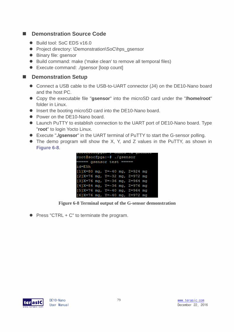
DE10-Nano
User Manual
79 www.terasic.com
December 22, 2016
Demonstration Source Code
Build tool: SoC EDS v16.0
Project directory: \Demonstration\SoC\hps_gsensor
Binary file: gsensor
Build command: make ('make clean' to remove all temporal files)
Execute command: ./gsensor [loop count]
Demonstration Setup
Connect a USB cable to the USB-to-UART connector (J4) on the DE10-Nano board
and the host PC.
Copy the executable file "gsensor" into the microSD card under the "/home/root"
folder in Linux.
Insert the booting microSD card into the DE10-Nano board.
Power on the DE10-Nano board.
Launch PuTTY to establish connection to the UART port of DE10-Nano board. Type
"root" to login Yocto Linux.
Execute "./gsensor" in the UART terminal of PuTTY to start the G-sensor polling.
The demo program will show the X, Y, and Z values in the PuTTY, as shown in
Figure 6-8.
Figure 6-8 Terminal output of the G-sensor demonstration
Press "CTRL + C" to terminate the program.
DE10-Nano
User Manual
80 www.terasic.com
December 22, 2016
Chapter 7 Examples
for using both HPS SoC and FGPA
his Chapter demonstrates how to use the HPS/ARM to communicate with FPGA. We
will introduce the GHRD project for DE10-Nano development board. And we develop
one ARM C Project which demonstrates how HPS/ARM program controls the ten
LEDs connected to FPGA. We will shows how HPS controls the FPGA LED through
Lightweight HPS-to-FPGA Bridge. The FPGA is configured by HPS through FPGA manager
in HPS.
7.1 RReeqquuiirreedd BBaacckkggrroouunndd
This section pre-assumed the developers have the following background knowledge:
FPGA RTL Design
Basic Quartus II operation skill
Basic RTL coding skill
Basic Qsys operation skill
Knowledge about Memory-Mapped Interface
C Program Design
Basic SoC EDS(Embedded Design Suite) operation skill
Basic C coding and compiling skill
Skill to Create a Linux Boot SD-Card for DE10-Nano with a given image file
Skill to boot Linux from SD-Card on DE10-Nano Skill to cope files into Linux file
system on DE10-Nano Basic Linux command operation skill
T
DE10-Nano
User Manual
81 www.terasic.com
December 22, 2016
7.2 SSyysstteemm RReeqquuiirreemmeennttss
Before starting this tutorial, please note that the following items are required to complete
the demonstration project:
Terasic DE10-Nano FPGA board, includes
Mini USB Cable for UART terminal
Micros SD-Card, at 4GB minimum
Micros SD-Card Card Reader
A x86 PC
Windows 7 64 bit operation system Installed
One USB Port
Quartus II 16.0 or Later Installed
SoC EDS 16.0 or Later Installed
Win32 Disk Imager Installed
7.3 AAXXII bbrriiddggeess iinn IInntteell SSooCC FFPPGGAA
In Intel SoC FPGA, the HPS logic and FPGA fabric are connected through the AXI
(Advanced eXtensible Interface) bridge. For HPS logic to communicate with FPGA fabric,
Intel system integration tool Qsys should be used for the system design to add HPS
component. From the AXI master port of the HPS component, HPS can access those Qsys
components whose memory-mapped slave ports are connected to the master port.
The HPS contains the following HPS-FPGA AXI bridges.
FPGA-to-HPS Bridge
HPS-to-FPGA Bridge
Lightweight HPS-to-FPGA Bridge
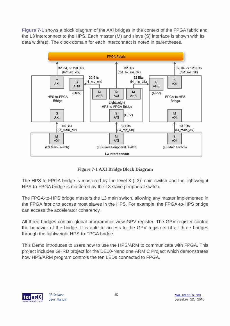
DE10-Nano
User Manual
82 www.terasic.com
December 22, 2016
Figure 7-1 shows a block diagram of the AXI bridges in the context of the FPGA fabric and
the L3 interconnect to the HPS. Each master (M) and slave (S) interface is shown with its
data width(s). The clock domain for each interconnect is noted in parentheses.
Figure 7-1 AXI Bridge Block Diagram
The HPS-to-FPGA bridge is mastered by the level 3 (L3) main switch and the lightweight
HPS-to-FPGA bridge is mastered by the L3 slave peripheral switch.
The FPGA-to-HPS bridge masters the L3 main switch, allowing any master implemented in
the FPGA fabric to access most slaves in the HPS. For example, the FPGA-to-HPS bridge
can access the accelerator coherency.
All three bridges contain global programmer view GPV register. The GPV register control
the behavior of the bridge. It is able to access to the GPV registers of all three bridges
through the lightweight HPS-to-FPGA bridge.
This Demo introduces to users how to use the HPS/ARM to communicate with FPGA. This
project includes GHRD project for the DE10-Nano one ARM C Project which demonstrates
how HPS/ARM program controls the ten LEDs connected to FPGA.
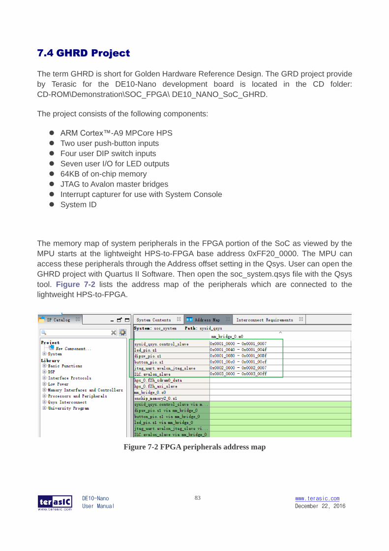
DE10-Nano
User Manual
83 www.terasic.com
December 22, 2016
7.4 GGHHRRDD PPrroojjeecctt
The term GHRD is short for Golden Hardware Reference Design. The GRD project provide
by Terasic for the DE10-Nano development board is located in the CD folder:
CD-ROM\Demonstration\SOC_FPGA\ DE10_NANO_SoC_GHRD.
The project consists of the following components:
ARM Cortex™-A9 MPCore HPS
Two user push-button inputs
Four user DIP switch inputs
Seven user I/O for LED outputs
64KB of on-chip memory
JTAG to Avalon master bridges
Interrupt capturer for use with System Console
System ID
The memory map of system peripherals in the FPGA portion of the SoC as viewed by the
MPU starts at the lightweight HPS-to-FPGA base address 0xFF20_0000. The MPU can
access these peripherals through the Address offset setting in the Qsys. User can open the
GHRD project with Quartus II Software. Then open the soc_system.qsys file with the Qsys
tool. Figure 7-2 lists the address map of the peripherals which are connected to the
lightweight HPS-to-FPGA.
Figure 7-2 FPGA peripherals address map
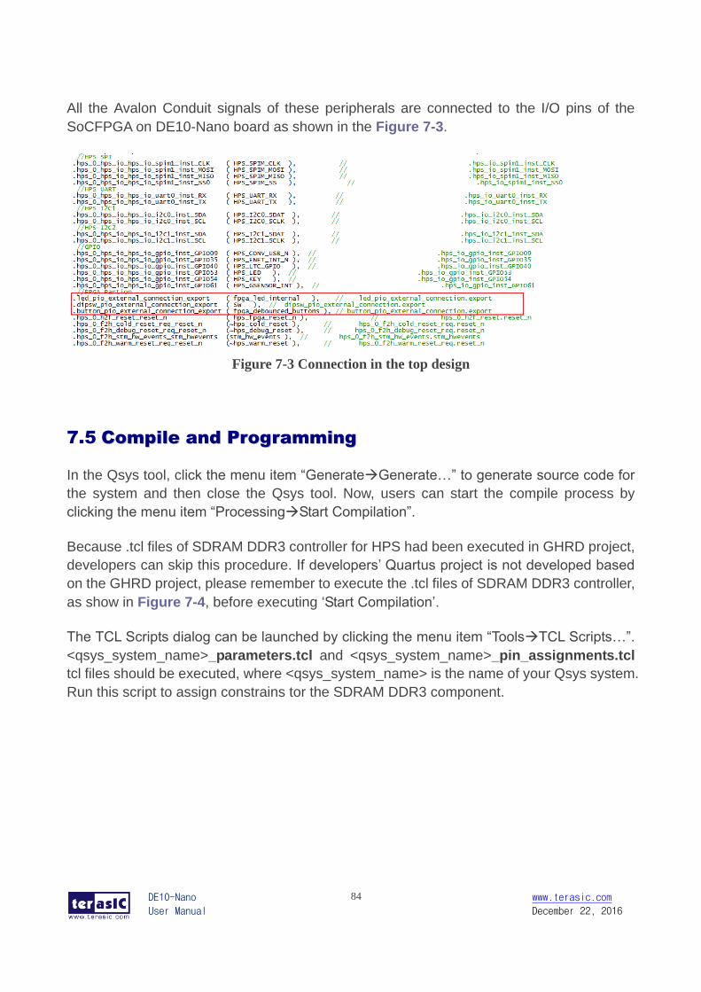
DE10-Nano
User Manual
84 www.terasic.com
December 22, 2016
All the Avalon Conduit signals of these peripherals are connected to the I/O pins of the
SoCFPGA on DE10-Nano board as shown in the Figure 7-3.
Figure 7-3 Connection in the top design
7.5 CCoommppiillee aanndd PPrrooggrraammmmiinngg
In the Qsys tool, click the menu item “GenerateGenerate…” to generate source code for
the system and then close the Qsys tool. Now, users can start the compile process by
clicking the menu item “ProcessingStart Compilation”.
Because .tcl files of SDRAM DDR3 controller for HPS had been executed in GHRD project,
developers can skip this procedure. If developers’ Quartus project is not developed based
on the GHRD project, please remember to execute the .tcl files of SDRAM DDR3 controller,
as show in Figure 7-4, before executing ‘Start Compilation’.
The TCL Scripts dialog can be launched by clicking the menu item “ToolsTCL Scripts…”.
<qsys_system_name>_parameters.tcl and <qsys_system_name>_pin_assignments.tcl
tcl files should be executed, where <qsys_system_name> is the name of your Qsys system.
Run this script to assign constrains tor the SDRAM DDR3 component.
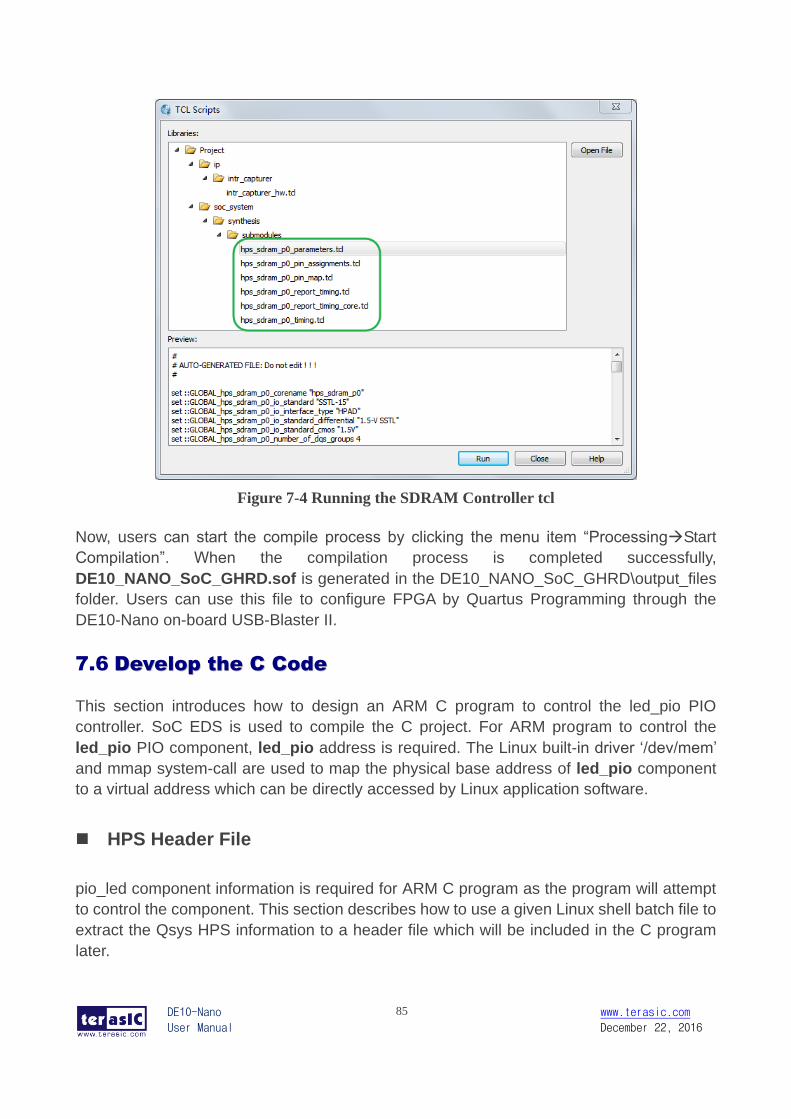
DE10-Nano
User Manual
85 www.terasic.com
December 22, 2016
Figure 7-4 Running the SDRAM Controller tcl
Now, users can start the compile process by clicking the menu item “ProcessingStart
Compilation”. When the compilation process is completed successfully,
DE10_NANO_SoC_GHRD.sof is generated in the DE10_NANO_SoC_GHRD\output_files
folder. Users can use this file to configure FPGA by Quartus Programming through the
DE10-Nano on-board USB-Blaster II.
7.6 DDeevveelloopp tthhee CC CCooddee
This section introduces how to design an ARM C program to control the led_pio PIO
controller. SoC EDS is used to compile the C project. For ARM program to control the
led_pio PIO component, led_pio address is required. The Linux built-in driver ‘/dev/mem’
and mmap system-call are used to map the physical base address of led_pio component
to a virtual address which can be directly accessed by Linux application software.
HPS Header File
pio_led component information is required for ARM C program as the program will attempt
to control the component. This section describes how to use a given Linux shell batch file to
extract the Qsys HPS information to a header file which will be included in the C program
later.
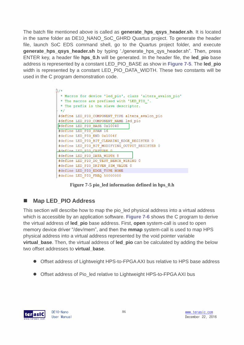
DE10-Nano
User Manual
86 www.terasic.com
December 22, 2016
The batch file mentioned above is called as generate_hps_qsys_header.sh. It is located
in the same folder as DE10_NANO_SoC_GHRD Quartus project. To generate the header
file, launch SoC EDS command shell, go to the Quartus project folder, and execute
generate_hps_qsys_header.sh by typing ‘./generate_hps_qys_header.sh”. Then, press
ENTER key, a header file hps_0.h will be generated. In the header file, the led_pio base
address is represented by a constant LED_PIO_BASE as show in Figure 7-5. The led_pio
width is represented by a constant LED_PIO_DATA_WIDTH. These two constants will be
used in the C program demonstration code.
Figure 7-5 pio_led information defined in hps_0.h
Map LED_PIO Address
This section will describe how to map the pio_led physical address into a virtual address
which is accessible by an application software. Figure 7-6 shows the C program to derive
the virtual address of led_pio base address. First, open system-call is used to open
memory device driver “/dev/mem”, and then the mmap system-call is used to map HPS
physical address into a virtual address represented by the void pointer variable
virtual_base. Then, the virtual address of led_pio can be calculated by adding the below
two offset addresses to virtual_base.
Offset address of Lightweight HPS-to-FPGA AXI bus relative to HPS base address
Offset address of Pio_led relative to Lightweight HPS-to-FPGA AXI bus
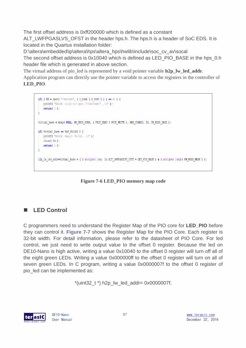
DE10-Nano
User Manual
87 www.terasic.com
December 22, 2016
The first offset address is 0xff200000 which is defined as a constant
ALT_LWFPGASLVS_OFST in the header hps.h. The hps.h is a header of SoC EDS. It is
located in the Quartus installation folder:
D:\altera\embedded\ip\altera\hps\altera_hps\hwlib\include\soc_cv_av\socal
The second offset address is 0x10040 which is defined as LED_PIO_BASE in the hps_0.h
header file which is generated in above section.
The virtual address of pio_led is represented by a void pointer variable h2p_lw_led_addr.
Application program can directly use the pointer variable to access the registers in the controller of
LED_PIO.
Figure 7-6 LED_PIO memory map code
LED Control
C programmers need to understand the Register Map of the PIO core for LED_PIO before
they can control it. Figure 7-7 shows the Register Map for the PIO Core. Each register is
32-bit width. For detail information, please refer to the datasheet of PIO Core. For led
control, we just need to write output value to the offset 0 register. Because the led on
DE10-Nano is high active, writing a value 0x10040 to the offset 0 register will turn off all of
the eight green LEDs. Writing a value 0x000000ff to the offset 0 register will turn on all of
seven green LEDs. In C program, writing a value 0x0000007f to the offset 0 register of
pio_led can be implemented as:
*(uint32_t *) h2p_lw_led_addr= 0x0000007f;
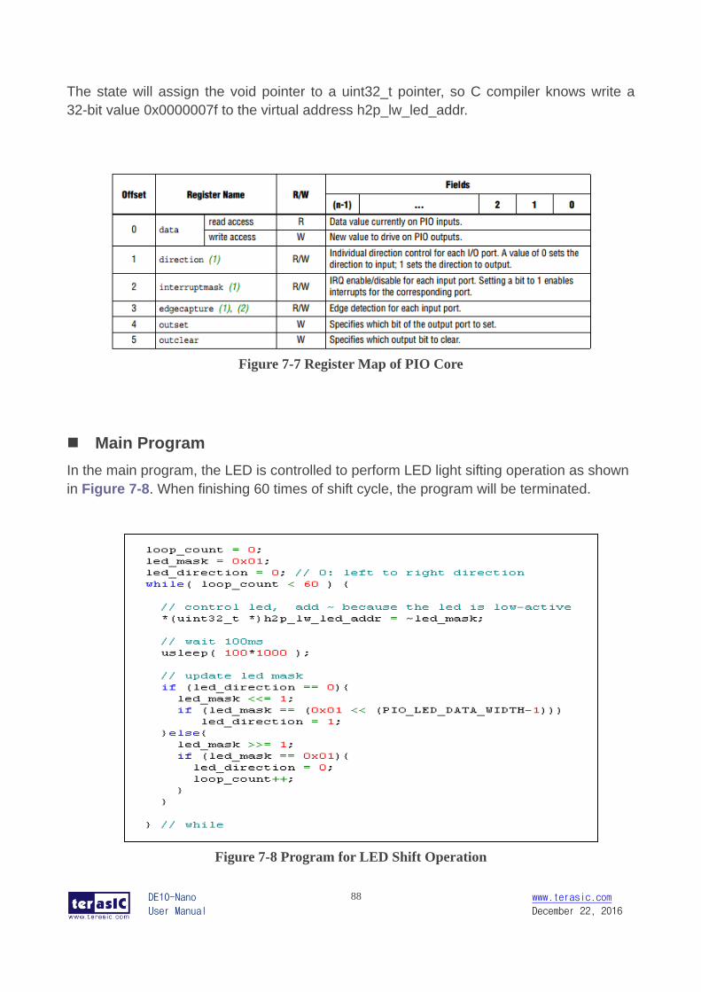
DE10-Nano
User Manual
88 www.terasic.com
December 22, 2016
The state will assign the void pointer to a uint32_t pointer, so C compiler knows write a
32-bit value 0x0000007f to the virtual address h2p_lw_led_addr.
Figure 7-7 Register Map of PIO Core
Main Program
In the main program, the LED is controlled to perform LED light sifting operation as shown
in Figure 7-8. When finishing 60 times of shift cycle, the program will be terminated.
Figure 7-8 Program for LED Shift Operation
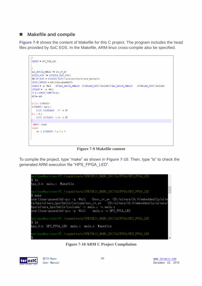
DE10-Nano
User Manual
89 www.terasic.com
December 22, 2016
Makefile and compile
Figure 7-9 shows the content of Makefile for this C project. The program includes the head
files provided by SoC EDS. In the Makefile, ARM-linux cross-compile also be specified.
Figure 7-9 Makefile content
To compile the project, type “make” as shown in Figure 7-10. Then, type “ls” to check the
generated ARM execution file “HPS_FPGA_LED”.
Figure 7-10 ARM C Project Compilation
DE10-Nano
User Manual
90 www.terasic.com
December 22, 2016
Execute the Demo
To execute the demo, please boot the Linux from the SD-card in DE10-Nano. Copy the
execution file “HPS_FPGA_LED” to the Linux directory, and type “chmod +x
HPS_FPGA_LED” to add execution attribute to the execute file. Use Quartus Programmer
to configure FPGA with the DE10_NANO_SoC_GHRD.sof generated in previous chapter.
The LED0 will flash as the heat beat of the FPGA. Then, type “./ HPS_FPGA_LED” to
launch the ARM program. The LED[7..1] on DE10-Nano I will be expected to perform 60
times of LED light shift operation, and then the program is terminated.
For details about booting the Linux from SD-card, please refer to the document:
DE10-Nano _Getting_Started_Guide.pdf
For details about copying files to Linux directory, please refer to the document:
My_First_HPS.pdf
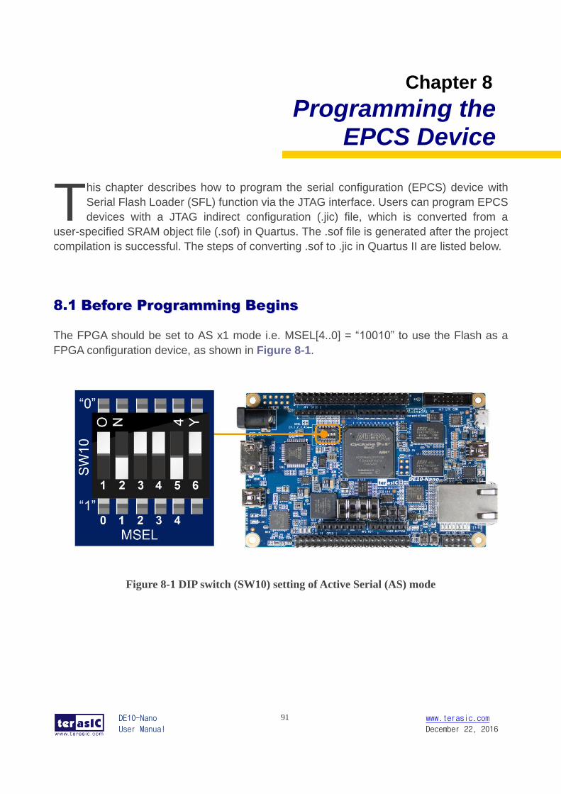
DE10-Nano
User Manual
91 www.terasic.com
December 22, 2016
Chapter 8 Programming the
EPCS Device
his chapter describes how to program the serial configuration (EPCS) device with
Serial Flash Loader (SFL) function via the JTAG interface. Users can program EPCS
devices with a JTAG indirect configuration (.jic) file, which is converted from a
user-specified SRAM object file (.sof) in Quartus. The .sof file is generated after the project
compilation is successful. The steps of converting .sof to .jic in Quartus II are listed below.
8.1 BBeeffoorree PPrrooggrraammmmiinngg BBeeggiinnss
The FPGA should be set to AS x1 mode i.e. MSEL[4..0] = “10010” to use the Flash as a
FPGA configuration device, as shown in Figure 8-1.
Figure 8-1 DIP switch (SW10) setting of Active Serial (AS) mode
T
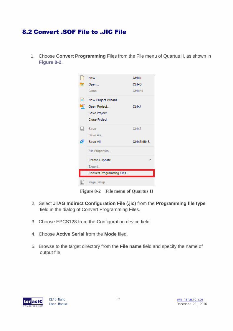
DE10-Nano
User Manual
92 www.terasic.com
December 22, 2016
8.2 CCoonnvveerrtt ..SSOOFF FFiillee ttoo ..JJIICC FFiillee
1. Choose Convert Programming Files from the File menu of Quartus II, as shown in
Figure 8-2.
Figure 8-2 File menu of Quartus II
2. Select JTAG Indirect Configuration File (.jic) from the Programming file type
field in the dialog of Convert Programming Files.
3. Choose EPCS128 from the Configuration device field.
4. Choose Active Serial from the Mode filed.
5. Browse to the target directory from the File name field and specify the name of
output file.
DE10-Nano
User Manual
93 www.terasic.com
December 22, 2016
6. Click on the SOF data in the section of Input files to convert, as shown in Figure
8-3.
Figure 8-3 Dialog of “Convert Programming Files”
7. Click Add File.
8. Select the .sof to be converted to a .jic file from the Open File dialog.
9. Click Open and the Convert Programming Files page will appear.
DE10-Nano
User Manual
94 www.terasic.com
December 22, 2016
10. Click on the Flash Loader and click Add Device, as shown in Figure 8-4.
Figure 8-4 Click on the “Flash Loader”
DE10-Nano
User Manual
95 www.terasic.com
December 22, 2016
11. The Select Devices page will appear, please select the targeted FPGA to be
programed into the EPCS, as shown in Figure 8-5.
Figure 8-5 “Select Devices” page
12. Click OK and the Convert Programming Files page will appear, as shown in Figure
8-6.
13. Click Generate.
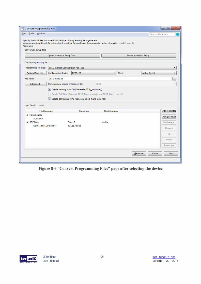
DE10-Nano
User Manual
96 www.terasic.com
December 22, 2016
Figure 8-6 “Convert Programming Files” page after selecting the device
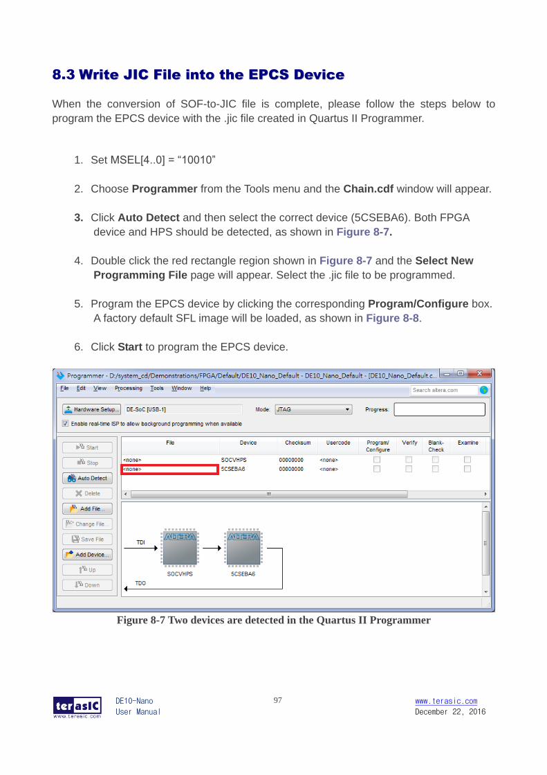
DE10-Nano
User Manual
97 www.terasic.com
December 22, 2016
8.3 WWrriittee JJIICC FFiillee iinnttoo tthhee EEPPCCSS DDeevviiccee
When the conversion of SOF-to-JIC file is complete, please follow the steps below to
program the EPCS device with the .jic file created in Quartus II Programmer.
1. Set MSEL[4..0] = “10010”
2. Choose Programmer from the Tools menu and the Chain.cdf window will appear.
3. Click Auto Detect and then select the correct device (5CSEBA6). Both FPGA
device and HPS should be detected, as shown in Figure 8-7.
4. Double click the red rectangle region shown in Figure 8-7 and the Select New
Programming File page will appear. Select the .jic file to be programmed.
5. Program the EPCS device by clicking the corresponding Program/Configure box.
A factory default SFL image will be loaded, as shown in Figure 8-8.
6. Click Start to program the EPCS device.
Figure 8-7 Two devices are detected in the Quartus II Programmer
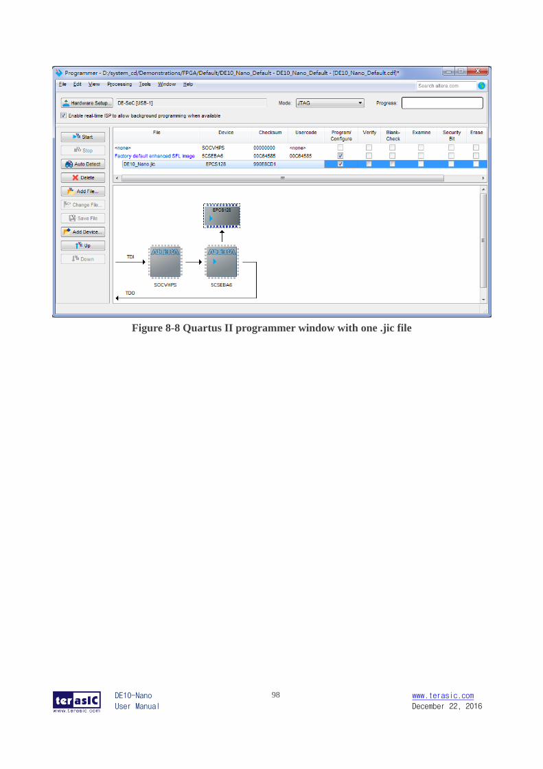
DE10-Nano
User Manual
98 www.terasic.com
December 22, 2016
Figure 8-8 Quartus II programmer window with one .jic file
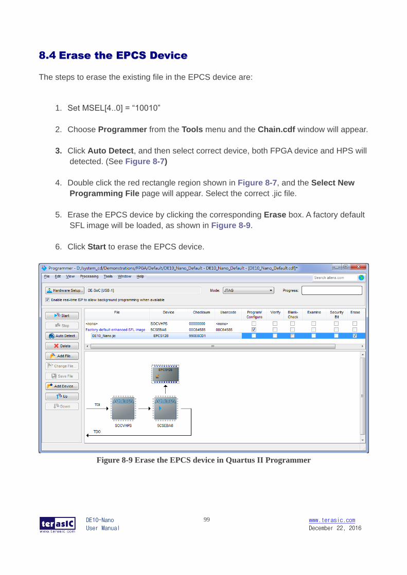
DE10-Nano
User Manual
99 www.terasic.com
December 22, 2016
8.4 EErraassee tthhee EEPPCCSS DDeevviiccee
The steps to erase the existing file in the EPCS device are:
1. Set MSEL[4..0] = “10010”
2. Choose Programmer from the Tools menu and the Chain.cdf window will appear.
3. Click Auto Detect, and then select correct device, both FPGA device and HPS will
detected. (See Figure 8-7)
4. Double click the red rectangle region shown in Figure 8-7, and the Select New
Programming File page will appear. Select the correct .jic file.
5. Erase the EPCS device by clicking the corresponding Erase box. A factory default
SFL image will be loaded, as shown in Figure 8-9.
6. Click Start to erase the EPCS device.
Figure 8-9 Erase the EPCS device in Quartus II Programmer
DE10-Nano
User Manual
100 www.terasic.com
December 22, 2016
8.5 EEPPCCSS PPrrooggrraammmmiinngg vviiaa nniiooss--22--ffllaasshh--pprrooggrraammmmeerr
Before programming the EPCS via nios-2-flash-programmer, users must add an EPCS
patch file nios-flash-override.txt into the Nios II EDS folder. The patch file is available in the
folder Demonstation\EPCS_Patch of DE10-Nano System CD. Please copy this file to the
folder [QuartusInstalledFolder]\nios2eds\bin (e.g. C:\altera\14.1\nios2eds\bin)
If the patch file is not included into the Nios II EDS folder, an error will occur as shown in
Figure 8-10.
Figure 8-10 Error Message “No EPCS Layout Data”.
8.6 NNiiooss IIII BBoooott ffrroomm EEPPCCSS DDeevviiccee iinn QQuuaarrttuuss IIII vv1144..11
There is a known problem in Quartus II software that the Quartus Programmer must be
used to program the EPCS device on DE10-Nano board. (Please refer to Intel’s website
here with details step by step.)
DE10-Nano
User Manual
101 www.terasic.com
December 22, 2016
Chapter 9 Appendix A
9.1 RReevviissiioonn HHiissttoorryy
Version Change Log
V1.0 Initial Version (Preliminary)
Copyright © 2016 Terasic Inc. All rights reserved.
Related Documents