CPLD and FPGA Gaurav Verma ECE Dept NIEC

Welcome message from author
This document is posted to help you gain knowledge. Please leave a comment to let me know what you think about it! Share it to your friends and learn new things together.
Transcript
CPLD and FPGA
Gaurav Verma
ECE Dept
NIEC
PLD • The first PLDs were Programmable Logic Arrays (PLAs).
• A PLA is a combinational, 2-level AND-OR device that can be
programmed to realise any sum-of-products logic expression.
• A PLA is limited by:
– the number of inputs (n)
– the number of outputs (m)
– the number of product terms (p)
• We refer to an “n x m PLA with p product terms”. Usually, p << 2 n.
• An n x m PLA with p product terms contains p 2n-input AND gates
and m p-input OR gates.

PLD
A 4x3 PLA with
6 product
terms.
• Each input is connected to a buffer that produces a true and a
complemented version of the signal.
•Potential connections are indicated by Xs. •The device is programmed by establishing the needed connections. •The connections are made by fuses.
Complex PLDs • What is the next step in the evolution of programmable
logic?
–More gates!
• How do we get more gates? • • We could put several PALs on one chip and put an
interconnection matrix between them!!
– This is called a Complex PLD (CPLD).
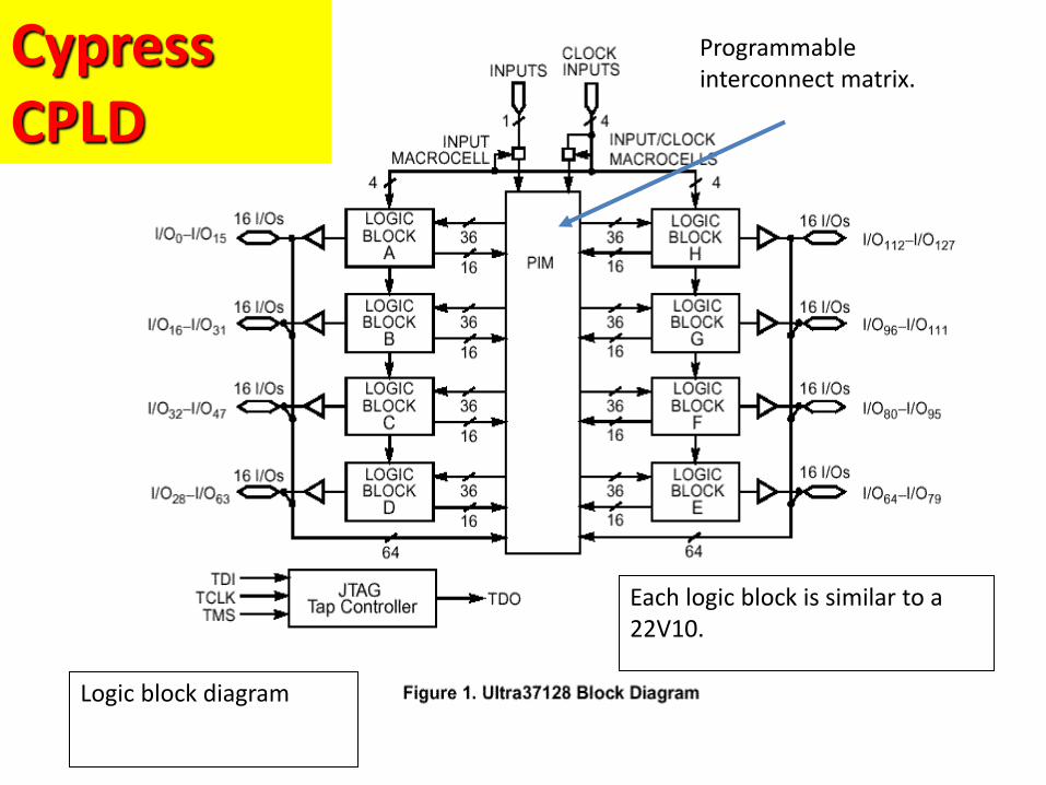
Cypress CPLD
Each logic block is similar to a 22V10.
Programmable interconnect matrix.
Logic block diagram
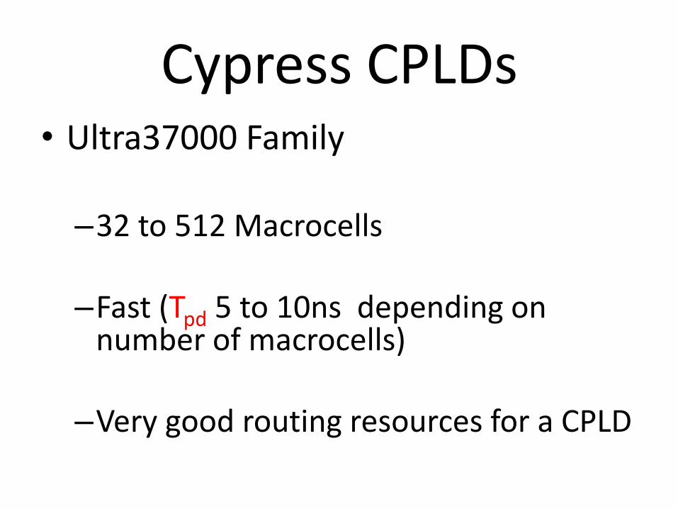
Cypress CPLDs • Ultra37000 Family
–32 to 512 Macrocells
–Fast (Tpd 5 to 10ns depending on
number of macrocells)
–Very good routing resources for a CPLD
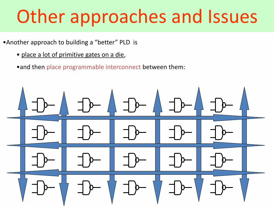
Other approaches and Issues •Another approach to building a “better” PLD is
• place a lot of primitive gates on a die,
•and then place programmable interconnect between them:

What is an FPGA? • Field Programmable Gate Array
• Fully programmable alternative to a customized chip
• Used to implement functions in hardware
• Also called a Reconfigurable Processing Unit (RPU)
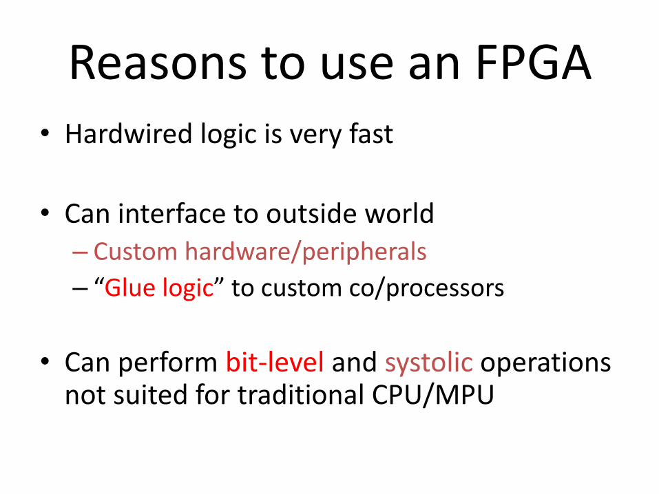
Reasons to use an FPGA • Hardwired logic is very fast
• Can interface to outside world – Custom hardware/peripherals
– “Glue logic” to custom co/processors
• Can perform bit-level and systolic operations not suited for traditional CPU/MPU
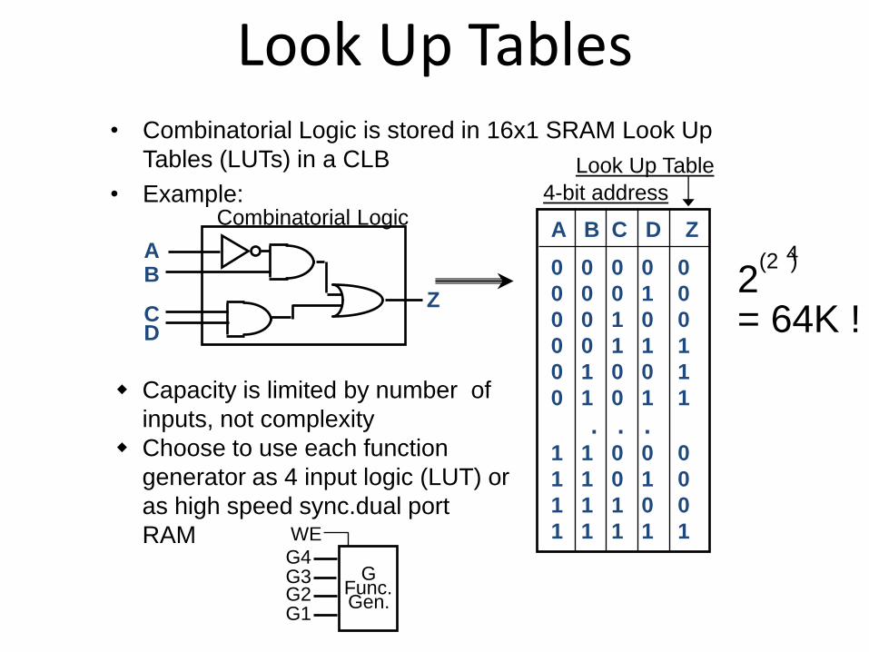
Look Up Tables
Capacity is limited by number of
inputs, not complexity
Choose to use each function
generator as 4 input logic (LUT) or
as high speed sync.dual port
RAM
• Combinatorial Logic is stored in 16x1 SRAM Look Up
Tables (LUTs) in a CLB
• Example:
A B C D Z
0 0 0 0 0
0 0 0 1 0
0 0 1 0 0
0 0 1 1 1
0 1 0 0 1
0 1 0 1 1
. . . 1 1 0 0 0
1 1 0 1 0
1 1 1 0 0
1 1 1 1 1
Look Up Table
Combinatorial Logic
A B
C D
Z
4-bit address
G Func. Gen.
G4 G3 G2 G1
WE
2 (2 ) 4
= 64K !
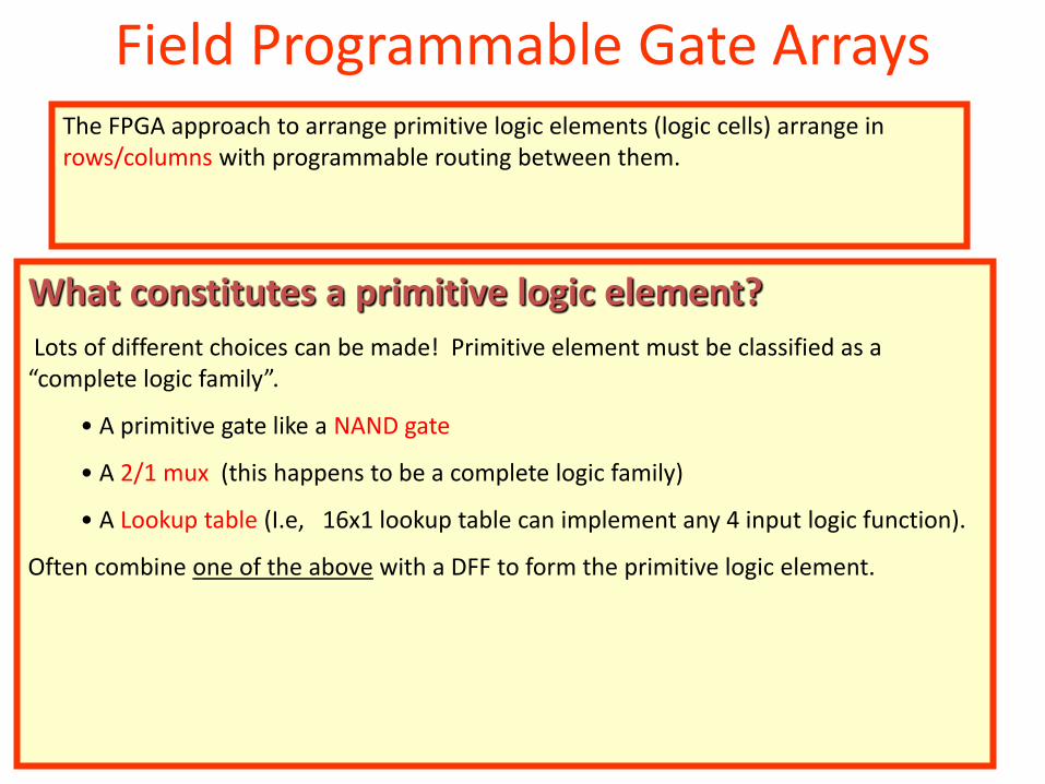
Field Programmable Gate Arrays The FPGA approach to arrange primitive logic elements (logic cells) arrange in rows/columns with programmable routing between them.
What constitutes a primitive logic element?
Lots of different choices can be made! Primitive element must be classified as a “complete logic family”.
• A primitive gate like a NAND gate
• A 2/1 mux (this happens to be a complete logic family)
• A Lookup table (I.e, 16x1 lookup table can implement any 4 input logic function).
Often combine one of the above with a DFF to form the primitive logic element.

Issues in FPGA Technologies • Complexity of Logic Element
– How many inputs/outputs for the logic element?
– Does the basic logic element contain a FF? What type?
• Interconnect
– How fast is it? Does it offer ‘high speed’ paths that cross the chip? How many of these?
– Can I have on-chip tri-state busses?
– How routable is the design? If 95% of the logic elements are used, can I route the design?
• More routing means more routability, but less room for logic elements
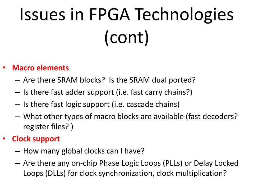
Issues in FPGA Technologies (cont)
• Macro elements
– Are there SRAM blocks? Is the SRAM dual ported?
– Is there fast adder support (i.e. fast carry chains?)
– Is there fast logic support (i.e. cascade chains)
– What other types of macro blocks are available (fast decoders? register files? )
• Clock support
– How many global clocks can I have?
– Are there any on-chip Phase Logic Loops (PLLs) or Delay Locked Loops (DLLs) for clock synchronization, clock multiplication?
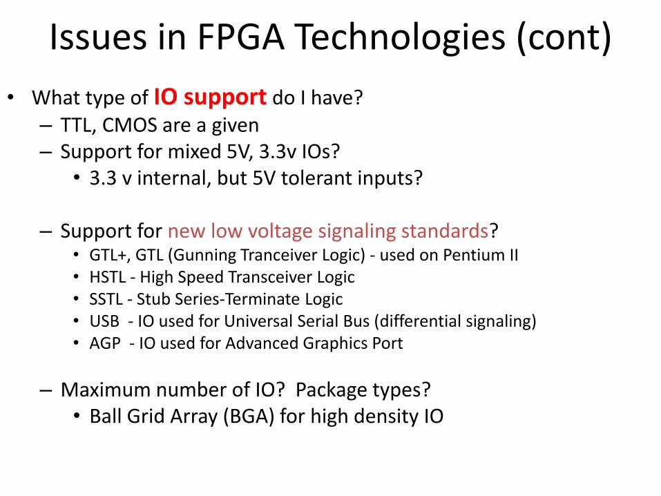
Issues in FPGA Technologies (cont)
• What type of IO support do I have? – TTL, CMOS are a given – Support for mixed 5V, 3.3v IOs?
• 3.3 v internal, but 5V tolerant inputs?
– Support for new low voltage signaling standards? • GTL+, GTL (Gunning Tranceiver Logic) - used on Pentium II • HSTL - High Speed Transceiver Logic • SSTL - Stub Series-Terminate Logic • USB - IO used for Universal Serial Bus (differential signaling) • AGP - IO used for Advanced Graphics Port
– Maximum number of IO? Package types? • Ball Grid Array (BGA) for high density IO

Altera FPGA Family • Altera Flex10K/10KE
– LEs (Logic elements) have 4-input LUTS (look-up tables) +1 FF
– Fast Carry Chain between LE’s, Cascade chain for logic operations
– Large blocks of SRAM available as well
• Altera Max7000/Max7000A – EEPROM based, very fast (Tpd = 7.5 ns)
– Basically a PLD architecture with programmable interconnect.
– Max 7000A family is 3.3 v

Altera Flex 10K FPGA Family
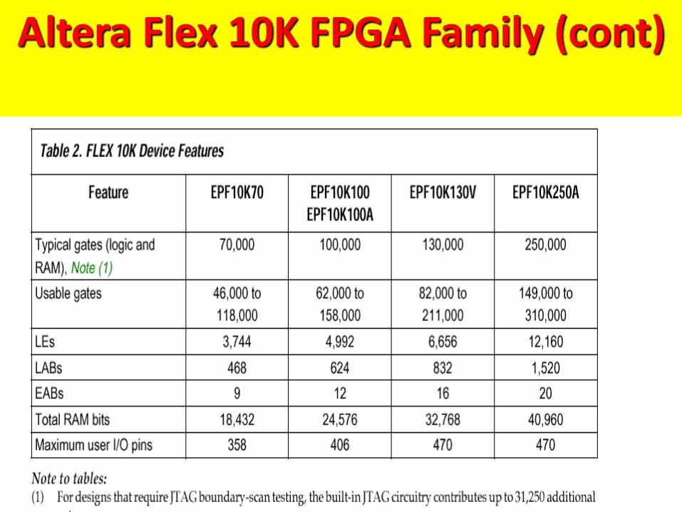
Altera Flex 10K FPGA Family (cont)

Dedicated memory
FLEX 10K Device Block Diagram
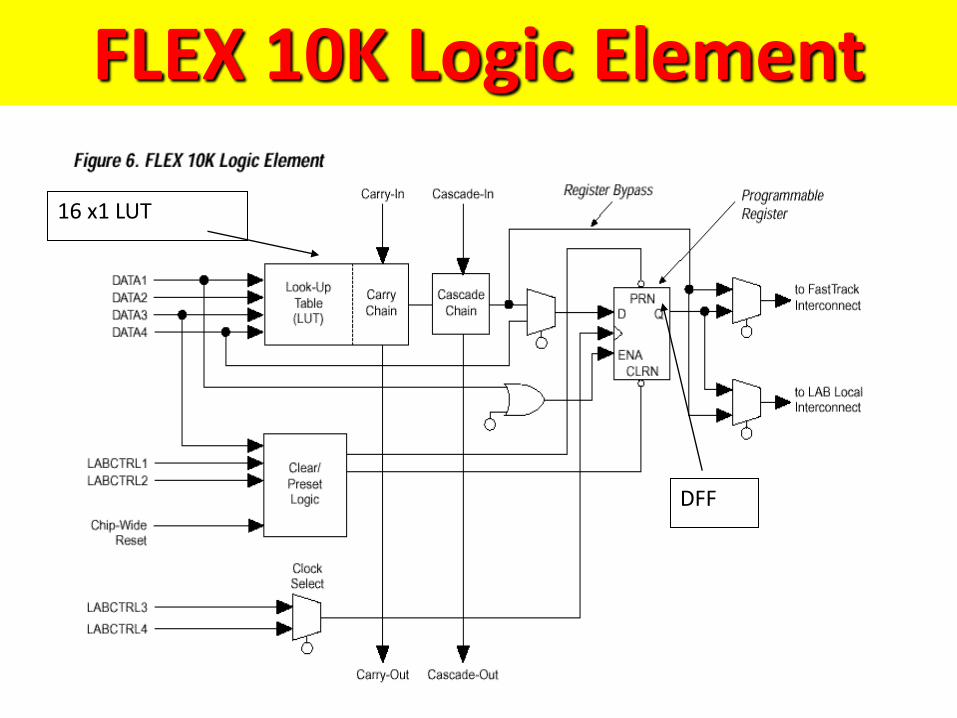
16 x1 LUT
DFF
FLEX 10K Logic Element
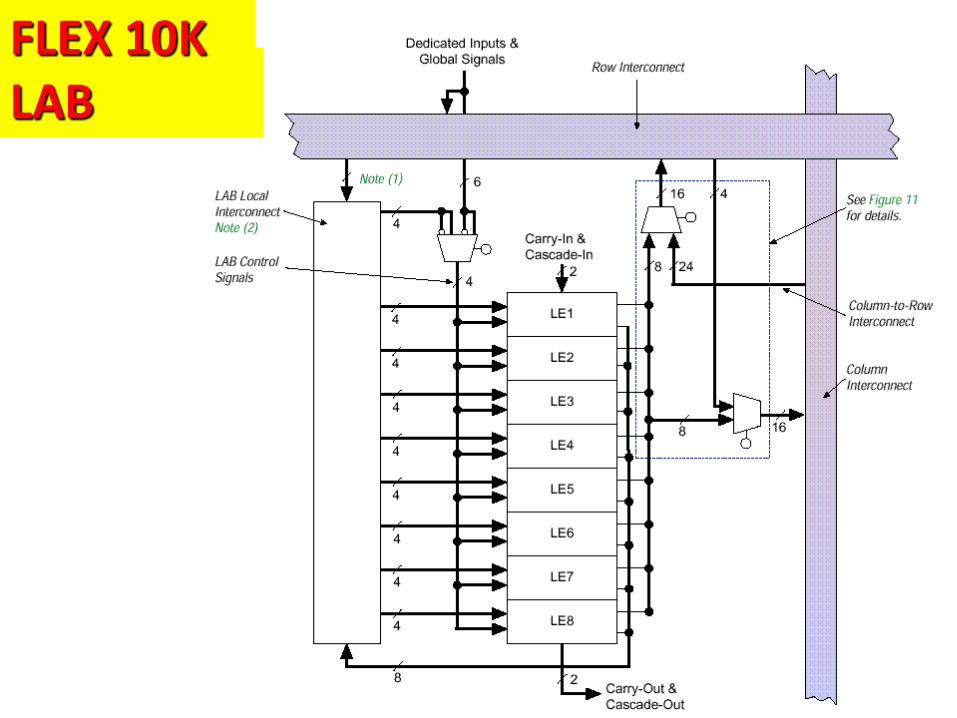
FLEX 10K LAB
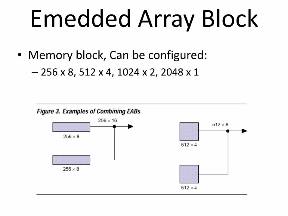
Emedded Array Block • Memory block, Can be configured:
– 256 x 8, 512 x 4, 1024 x 2, 2048 x 1

Actel FPGA Family • MXDS Family
– Fine grain Logic Elements that contain Mux logic + DFF
– Embedded Dual Port SRAM
– One Time Programmable (OTP) - means that no configuration loading on powerup, no external serial ROM
– AntiFuse technology for programming (AntiFuse means that you program the fuse to make the connection).
– Fast (Tpd = 7.5 ns)
– Low density compared to Altera, Xilinx - maximum number of gates is 36,000
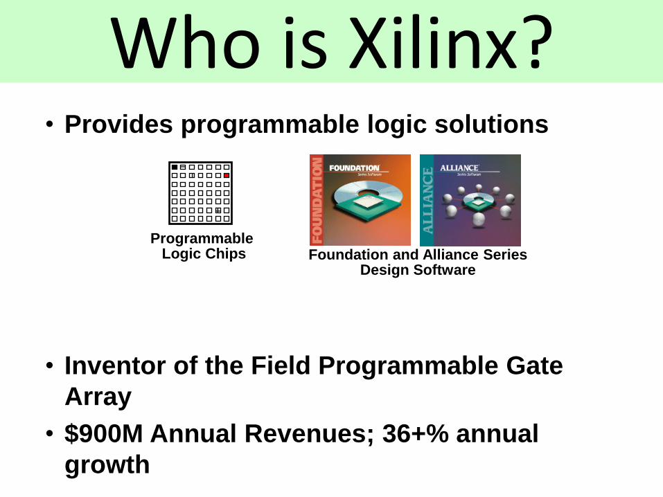
Who is Xilinx? • Provides programmable logic solutions
• Inventor of the Field Programmable Gate
Array
• $900M Annual Revenues; 36+% annual
growth
Programmable Logic Chips Foundation and Alliance Series
Design Software

Xilinx FPGA Family • Virtex Family
– SRAM Based
– Largest device has 1M gates
– Configurable Logic Blocks (CLBs) have two 4-input LUTS, 2 DFFs
– Four onboard Delay Locked Loops (DLLs) for clock synchronization
– Dedicated RAM blocks (LUTs can also function as RAM).
– Fast Carry Logic
• XC4000 Family
– Previous version of Virtex
– No DLLs, No dedicated RAM blocks

XC4000 Architecture
CLB
CLB
CLB
CLB
Switch
Matrix
Programmable
Interconnect I/O Blocks (IOBs)
Configurable
Logic Blocks (CLBs)
D Q
SlewRate
Control
PassivePull-Up,
Pull-Down
Delay
Vcc
Output
Buffer
Input
Buffer
Q D
Pad
D Q
SD
RD
EC
S/R
Control
D Q
SD
RD
EC
S/R
Control
1
1
F'
G'
H'
DIN
F'
G'
H'
DIN
F'
G'
H'
H'
HFunc.Gen.
GFunc.Gen.
FFunc.Gen.
G4G3G2G1
F4F3F2F1
C4C1 C2 C3
K
Y
X
H1 DIN S/R EC
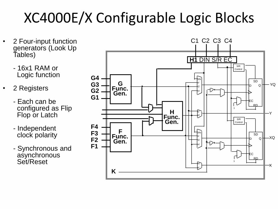
XC4000E/X Configurable Logic Blocks
D Q
SD
RD
EC
S/R
Control
D Q
SD
RD
EC
S/R
Control
1
1
F'
G'
H'
DIN
F'
G'
H'
DIN
F'
G'
H'
H'
H Func. Gen.
G Func. Gen.
F Func. Gen.
G4 G3 G2 G1
F4 F3 F2 F1
C4 C1 C2 C3
K
YQ
Y
XQ
X
H1 DIN S/R EC
• 2 Four-input function generators (Look Up Tables)
- 16x1 RAM or Logic function
• 2 Registers
- Each can be configured as Flip Flop or Latch - Independent clock polarity - Synchronous and asynchronous Set/Reset

ALTERA CYCLONE PROCESSOR
The Cyclone device family offers the following features: ■ 2,910 to 20,060 LEs, see Table 1–1 ■ Up to 294,912 RAM bits (36,864 bytes) ■ Supports configuration through low-cost serial configuration device ■ Support for LVTTL, LVCMOS, SSTL-2, and SSTL-3 I/O standards ■ Support for 66- and 33-MHz, 64- and 32-bit PCI standard ■ High-speed (640 Mbps) LVDS I/O support ■ Low-speed (311 Mbps) LVDS I/O support ■ 311-Mbps RSDS I/O support ■ Up to two PLLs per device provide clock multiplication and phase shifting ■ Up to eight global clock lines with six clock resources available per logic array block (LAB) row ■ Support for external memory, including DDR SDRAM (133 MHz), FCRAM, and single data rate (SDR) SDRAM ■ Support for multiple intellectual property (IP) cores, including Altera MegaCore functions and Altera Mega functions Partners Program (AMPPSM) megafunctions.

=> Cyclone® devices contain a two-dimensional row- and column-based architecture to implement custom logic. Column and row interconnects of varying speeds provide signal interconnects between LABs and embedded memory blocks.
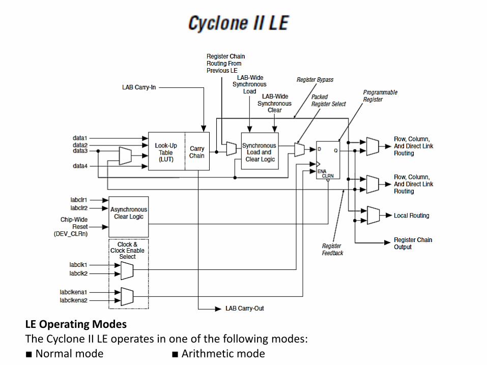
LE Operating Modes The Cyclone II LE operates in one of the following modes: ■ Normal mode ■ Arithmetic mode

Normal Mode The normal mode is suitable for general logic applications and combinational functions. In normal mode, four data inputs from the LAB local interconnect are inputs to a four-input LUT . The Quartus II Compiler automatically selects the carry-in or the data3 signal as one of the inputs to the LUT. LEs in normal mode support packed registers and register feedback.
Normal Mode

Arithmetic Mode The arithmetic mode is ideal for implementing adders, counters, accumulators, and comparators. An LE in arithmetic mode implements a 2-bit full adder and basic carry chain (see Figure 2–4). LEs in arithmetic mode can drive out registered and unregistered versions of the LUT output. Register feedback and register packing are supported when LEs are used in arithmetic mode.
LE in Normal Mode
Related Documents


![index [portal.unimap.edu.my]portal.unimap.edu.my/portal/page/portal30/Lecture Notes...Programmable Logic Devices (PLDs) are ICs with a large number of gates and flip flops that can](https://static.cupdf.com/doc/110x72/5e7054cbeb00c9419349ced3/index-notes-programmable-logic-devices-plds-are-ics-with-a-large-number.jpg)

