DC to 9 GHz Vector Signal Generator Data Sheet AD9166 Rev. 0 Document Feedback Information furnished by Analog Devices is believed to be accurate and reliable. However, no responsibility is assumed by Analog Devices for its use, nor for any infringements of patents or other rights of third parties that may result from its use. Specifications subject to change without notice. No license is granted by implication or otherwise under any patent or patent rights of Analog Devices. Trademarks and registered trademarks are the property of their respective owners. One Technology Way, P.O. Box 9106, Norwood, MA 02062-9106, U.S.A. Tel: 781.329.4700 ©2020 Analog Devices, Inc. All rights reserved. Technical Support www.analog.com FEATURES DC-coupled, 50 Ω matched output Up to 4.3 dBm output power, −9.5 dBm at 9 GHz DAC core update rate: 12.0 GSPS (guaranteed minimum) in 2× NRZ mode Wide analog bandwidth DC to 9.0 GHz in 2× NRZ mode (12.0 GSPS DAC update rate) 1.0 GHz to 8.0 GHz in mix mode (6.0 GSPS DAC update rate) DC to 4.5 GHz in NRZ mode (6.0 GSPS DAC update rate) Power dissipation of 4.88 W in 2× NRZ mode (10 GSPS DAC update rate) Bypassable datapath interpolation 2×, 3×, 4×, 6×, 8×, 12×, 16×, 24× Instantaneous (complex) signal bandwidth 2.25 GHz with device clock at 5 GHz (2× interpolation) 1.8 GHz with device clock at 6 GHz (3× interpolation) Fast frequency hopping Integrated BiCMOS buffer amplifier APPLICATIONS Instrumentation: automated test equipment, electronic test and measurement, arbitrary waveform generators Electronic warfare: radars, jammers Broadband communications systems Local oscillator drivers GENERAL DESCRIPTION The AD9166 1 is a high performance, wideband, on-chip vector signal generator composed of a high speed JESD204B serializer/ deserializer (SERDES) interface, a flexible 16-bit digital datapath, a inphase/quadrature (I/Q) digital-to-analog converter (DAC) core, and an integrated differential to single-ended output buffer amplifier, matched to a 50 Ω load up to 10 GHz. The DAC core is based on a quad-switch architecture, which is configurable to increase the effective DAC core update rate of up to 12.8 GSPS from a 6.4 GHz DAC sampling clock, with an analog output bandwidth of true dc to 9.0 GHz, typically. The digital datapath includes multiple interpolation filter stages, a direct digital synthesizer (DDS) block with multiple numerically controlled oscillators (NCOs) supporting fast frequency hopping (FFH), and additional FIR85 and inverse sinc filter stages to allow flexible spectrum planning. The differential to single-ended buffer eliminates the need for a wideband balun, and supports the full analog output bandwidth of the DAC core. DC coupling the output allows baseband wave- form generation without the need for external bias tees or similar circuitry, which makes the AD9166 uniquely suited for the most demanding high speed ultrawideband RF transmit applications. The various filter stages enable the AD9166 to be configured for lower data rates, while maintaining higher DAC clock rates to ease the filtering requirements and reduce the overall system size, weight, and power. The data interface receiver consists of up to eight JESD204B SERDES lanes, each capable of carrying up to 12.5 Gbps. To enable maximum flexibility, the receiver is fully configurable according to the data rate, number of SERDES lanes, and lane mapping required by the JESD204B transmitter. In 2× nonreturn-to-zero (NRZ) mode of operation (with FIR85 enabled), the AD9166 can reconstruct RF carriers from true dc to the edge of the third Nyquist zone, or an analog bandwidth of true dc up to 9 GHz. In mix mode, the AD9166 can reconstruct RF carriers in the second and third Nyquist zones while consuming lower power and maintaining a performance comparable to 2× NRZ mode. In baseband modes, such as return-to-zero (RZ) and 1× NRZ, the AD9166 is ideal to reconstruct RF carriers from true dc to the edge of the first Nyquist zone while consuming lower power compared to 2× NRZ mode. The quadrature DDS block can be configured as a digital upconverter to upconvert I/Q data samples to the desired location across the spectrum, in all three Nyquist zones. The DDS also consists of a bank of 32 numerically controlled oscillators (NCOs), each with its own 32-bit phase accumulator. When combined with a 100 MHz serial peripheral interface (SPI), the DDS allows a phase coherent FFH, with a phase settling time as low as 300 ns. The AD9166 is configured using a common SPI interface that monitors the status of all registers. The AD9166 is offered in a 324-ball, 15 mm × 15 mm, 0.8 mm pitch BGA_ED package. PRODUCT HIGHLIGHTS 1. High dynamic range and signal reconstruction bandwidth supports RF signal synthesis of up to 9 GHz. 2. Fully supports zero IF and other dc-coupled applications. 3. Up to an eight-lane JESD204B SERDES interface, with various features to allow flexibility when interfacing to a JESD204B transmitter. 1 Protected by U.S. Patents 6,842,132 and 7,796,971.

Welcome message from author
This document is posted to help you gain knowledge. Please leave a comment to let me know what you think about it! Share it to your friends and learn new things together.
Transcript
DC to 9 GHz Vector Signal GeneratorData Sheet AD9166
Rev. 0 Document Feedback Information furnished by Analog Devices is believed to be accurate and reliable. However, no responsibility is assumed by Analog Devices for its use, nor for any infringements of patents or other rights of third parties that may result from its use. Specifications subject to change without notice. No license is granted by implication or otherwise under any patent or patent rights of Analog Devices. Trademarks and registered trademarks are the property of their respective owners.
One Technology Way, P.O. Box 9106, Norwood, MA 02062-9106, U.S.A.Tel: 781.329.4700 ©2020 Analog Devices, Inc. All rights reserved. Technical Support www.analog.com
FEATURES DC-coupled, 50 Ω matched output Up to 4.3 dBm output power, −9.5 dBm at 9 GHz DAC core update rate: 12.0 GSPS (guaranteed minimum) in
2× NRZ mode Wide analog bandwidth
DC to 9.0 GHz in 2× NRZ mode (12.0 GSPS DAC update rate) 1.0 GHz to 8.0 GHz in mix mode (6.0 GSPS DAC update rate) DC to 4.5 GHz in NRZ mode (6.0 GSPS DAC update rate)
Power dissipation of 4.88 W in 2× NRZ mode (10 GSPS DAC update rate)
Bypassable datapath interpolation 2×, 3×, 4×, 6×, 8×, 12×, 16×, 24×
Instantaneous (complex) signal bandwidth 2.25 GHz with device clock at 5 GHz (2× interpolation) 1.8 GHz with device clock at 6 GHz (3× interpolation)
Fast frequency hopping Integrated BiCMOS buffer amplifier
APPLICATIONS Instrumentation: automated test equipment, electronic test
and measurement, arbitrary waveform generators Electronic warfare: radars, jammers Broadband communications systems Local oscillator drivers
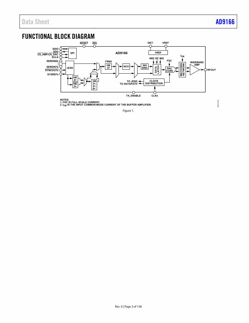
GENERAL DESCRIPTION The AD91661 is a high performance, wideband, on-chip vector signal generator composed of a high speed JESD204B serializer/ deserializer (SERDES) interface, a flexible 16-bit digital datapath, a inphase/quadrature (I/Q) digital-to-analog converter (DAC) core, and an integrated differential to single-ended output buffer amplifier, matched to a 50 Ω load up to 10 GHz.
The DAC core is based on a quad-switch architecture, which is configurable to increase the effective DAC core update rate of up to 12.8 GSPS from a 6.4 GHz DAC sampling clock, with an analog output bandwidth of true dc to 9.0 GHz, typically. The digital datapath includes multiple interpolation filter stages, a direct digital synthesizer (DDS) block with multiple numerically controlled oscillators (NCOs) supporting fast frequency hopping (FFH), and additional FIR85 and inverse sinc filter stages to allow flexible spectrum planning.
The differential to single-ended buffer eliminates the need for a wideband balun, and supports the full analog output bandwidth of the DAC core. DC coupling the output allows baseband wave-
form generation without the need for external bias tees or similar circuitry, which makes the AD9166 uniquely suited for the most demanding high speed ultrawideband RF transmit applications.
The various filter stages enable the AD9166 to be configured for lower data rates, while maintaining higher DAC clock rates to ease the filtering requirements and reduce the overall system size, weight, and power.
The data interface receiver consists of up to eight JESD204B SERDES lanes, each capable of carrying up to 12.5 Gbps. To enable maximum flexibility, the receiver is fully configurable according to the data rate, number of SERDES lanes, and lane mapping required by the JESD204B transmitter.
In 2× nonreturn-to-zero (NRZ) mode of operation (with FIR85 enabled), the AD9166 can reconstruct RF carriers from true dc to the edge of the third Nyquist zone, or an analog bandwidth of true dc up to 9 GHz.
In mix mode, the AD9166 can reconstruct RF carriers in the second and third Nyquist zones while consuming lower power and maintaining a performance comparable to 2× NRZ mode.
In baseband modes, such as return-to-zero (RZ) and 1× NRZ, the AD9166 is ideal to reconstruct RF carriers from true dc to the edge of the first Nyquist zone while consuming lower power compared to 2× NRZ mode.
The quadrature DDS block can be configured as a digital upconverter to upconvert I/Q data samples to the desired location across the spectrum, in all three Nyquist zones.
The DDS also consists of a bank of 32 numerically controlled oscillators (NCOs), each with its own 32-bit phase accumulator. When combined with a 100 MHz serial peripheral interface (SPI), the DDS allows a phase coherent FFH, with a phase settling time as low as 300 ns.
The AD9166 is configured using a common SPI interface that monitors the status of all registers. The AD9166 is offered in a 324-ball, 15 mm × 15 mm, 0.8 mm pitch BGA_ED package.
PRODUCT HIGHLIGHTS 1. High dynamic range and signal reconstruction bandwidth
supports RF signal synthesis of up to 9 GHz. 2. Fully supports zero IF and other dc-coupled applications. 3. Up to an eight-lane JESD204B SERDES interface, with
various features to allow flexibility when interfacing to a JESD204B transmitter.
1 Protected by U.S. Patents 6,842,132 and 7,796,971.
AD9166 Data Sheet
Rev. 0 | Page 2 of 138
TABLE OF CONTENTS Features .............................................................................................. 1 Applications ....................................................................................... 1 General Description ......................................................................... 1 Product Highlights ........................................................................... 1 Revision History ............................................................................... 2 Functional Block Diagram .............................................................. 3 Specifications ..................................................................................... 4
DC Specifications ......................................................................... 4 Power Supply DC Specifications ................................................ 5 Device Input Clock Rate and DAC Update Rate Specifications ......................................................................................................... 7 JESD204B Interface Specifications ............................................. 8 Input Data Rate and Bandwidth Specifications ........................ 9 Pipeline Delay and Latency Uncertainty Specifications .......... 9 AC Specifications ........................................................................ 10 CMOS Pin Specifications .......................................................... 11 Timing Specifications ................................................................ 12
Absolute Maximum Ratings .......................................................... 14 Reflow Profile .............................................................................. 14 Thermal Management ............................................................... 14 Thermal Resistance .................................................................... 14 ESD Caution ................................................................................ 14
Pin Configuration and Function Descriptions ........................... 15 Typical Performance Characteristics ........................................... 18
AC Performance (2× NRZ (FIR85) Mode) ............................. 18 LTE Performance (2× NRZ (FIR85) Mode) ........................... 23 802.11AC Performance (2× NRZ (FIR85) Mode) ................. 24
Terminology .................................................................................... 25 Theory of Operation ...................................................................... 26 Serial Port Operation ..................................................................... 27
Data Format ................................................................................ 27 Serial Port Pin Descriptions ...................................................... 27 Serial Port Options ..................................................................... 28
JESD204B Serial Data Interface .................................................... 29
JESD204B Overview .................................................................. 29 Physical Layer ............................................................................. 31 Data Link Layer .......................................................................... 34 Transport Layer .......................................................................... 42 JESD204B Test Modes ............................................................... 44 JESD204B Error Monitoring ..................................................... 46 Hardware Considerations ......................................................... 48
Main Digital Datapath ................................................................... 49 Data Format ................................................................................ 49 Interpolation Filters ................................................................... 49 Digital Modulation ..................................................................... 52 Inverse Sinc ................................................................................. 55 Downstream Protection ............................................................ 55 Datapath PRBS ........................................................................... 56 Datapath PRBS IRQ ................................................................... 56
Interrupt Request Operation ........................................................ 57 Interrupt Service Routine .......................................................... 57
Applications Information .............................................................. 58 Hardware Considerations ......................................................... 58
Analog Interface Considerations .................................................. 61 Analog Modes of Operation ..................................................... 61 Clock Input .................................................................................. 62 Shuffle Mode ............................................................................... 63 Voltage Reference and Full-Scale Current (FSC) ................... 63 Analog Output ............................................................................ 64 Temperature Sensors .................................................................. 65
Start-Up Sequence .......................................................................... 67 Register Summary: DAC ............................................................... 70 Register Details: DAC Register Map ............................................ 79 Register Summary: Amplifier ..................................................... 135 Register Details: Amplifier Register Map .................................. 136 Outline Dimensions ..................................................................... 138
Ordering Guide ........................................................................ 138
REVISION HISTORY 7/2020—Revision 0: Initial Version
Data Sheet AD9166
Rev. 0 | Page 3 of 138
FUNCTIONAL BLOCK DIAGRAM
HB2×HB3×
JESD
HB2×,4×,8×
INVSINC
DAT
ALA
TCH
SDOSDIO
SCLKCS_AMP/CS_DAC SPI
DACCORE
SERDIN0±
SERDIN7±
SYSREF±SYNCOUT±
CLOCKDISTRIBUTION
MA
TCH
ING
NETW
ORK
WIDEBANDAMP
CLK±
AD9166
TO JESDTO DATAPATH
TX_ENABLE
RFOUT
RESET IRQ
VREF
ISET VREF
NCOHB2×
FIR85NRZ RZ
FSC
ICMMIX
2081
0-00
1NOTES1. FSC IS FULL-SCALE CURRENT.2. ICM IS THE INPUT COMMON-MODE CURRENT OF THE BUFFER AMPLIFIER.
Figure 1.
AD9166 Data Sheet
Rev. 0 | Page 4 of 138
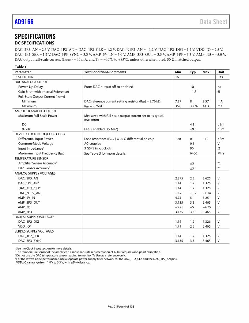
SPECIFICATIONS DC SPECIFICATIONS DAC_2P5_AN = 2.5 V, DAC_1P2_AN = DAC_1P2_CLK = 1.2 V, DAC_N1P2_AN = −1.2 V, DAC_1P2_DIG = 1.2 V, VDD_IO = 2.5 V, DAC_1P2_SER = 1.2 V, DAC_3P3_SYNC = 3.3 V, AMP_5V_IN = 5.0 V, AMP_3P3_OUT = 3.3 V, AMP_3P3 = 3.3 V, AMP_N5 = −5.0 V, DAC output full-scale current (IOUTFS) = 40 mA, and TA = −40°C to +85°C, unless otherwise noted. 50 Ω matched output.
Table 1. Parameter Test Conditions/Comments Min Typ Max Unit RESOLUTION 16 Bits
DAC ANALOG OUTPUT Power-Up Delay From DAC output off to enabled 10 ns Gain Error (with Internal Reference) −1.7 %
Full-Scale Output Current (IOUTFS)
Minimum DAC reference current setting resistor (RSET) = 9.76 kΩ 7.37 8 8.57 mA Maximum RSET = 9.76 kΩ 35.8 38.76 41.3 mA
AMPLIFIER ANALOG OUTPUT Maximum Full-Scale Power Measured with full-scale output current set to its typical
maximum
DC 4.3 dBm 9 GHz FIR85 enabled (2× NRZ) −9.5 dBm
DEVICE CLOCK INPUT (CLK+, CLK−) Differential Input Power Load resistance (RLOAD) = 90 Ω differential on chip −20 0 +10 dBm Common-Mode Voltage AC-coupled 0.6 V
Input Impedance1 3 GSPS input clock 90 Ω
Maximum Input Frequency (fCLK) See Table 3 for more details 6400 MHz
TEMPERATURE SENSOR Amplifier Sensor Accuracy2 ±5 °C
DAC Sensor Accuracy3 ±5 °C
ANALOG SUPPLY VOLTAGES
DAC_2P5_AN 2.375 2.5 2.625 V
DAC_1P2_AN4 1.14 1.2 1.326 V
DAC_1P2_CLK4 1.14 1.2 1.326 V
DAC_N1P2_AN −1.26 −1.2 −1.14 V AMP_5V_IN 4.75 5 5.25 V AMP_3P3_OUT 3.135 3.3 3.465 V AMP_N5 −5.25 −5 −4.75 V AMP_3P3 3.135 3.3 3.465 V
DIGITAL SUPPLY VOLTAGES DAC_1P2_DIG 1.14 1.2 1.326 V VDD_IO5 1.71 2.5 3.465 V
SERDES SUPPLY VOLTAGES DAC_1P2_SER 1.14 1.2 1.326 V DAC_3P3_SYNC 3.135 3.3 3.465 V
1 See the Clock Input section for more details. 2 The temperature sensor of the amplifier is a more accurate representation of TJ, but requires one-point calibration. 3 Do not use the DAC temperature sensor reading to monitor TJ. Use as a reference only. 4 For the lowest noise performance, use a separate power supply filter network for the DAC_1P2_CLK and the DAC_1P2_AN pins. 5 VDD_IO can range from 1.8 V to 3.3 V, with ±5% tolerance.
Data Sheet AD9166
Rev. 0 | Page 5 of 138
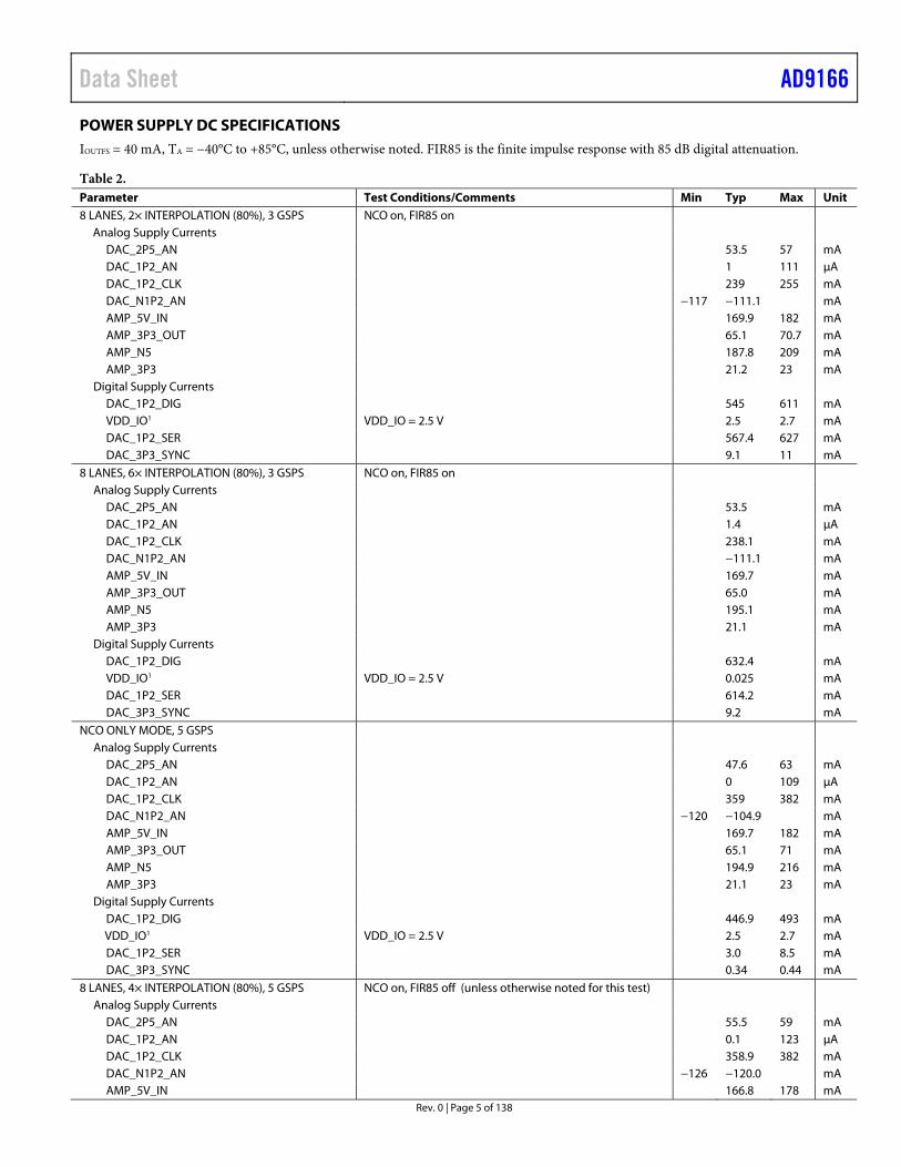
POWER SUPPLY DC SPECIFICATIONS IOUTFS = 40 mA, TA = −40°C to +85°C, unless otherwise noted. FIR85 is the finite impulse response with 85 dB digital attenuation.
Table 2. Parameter Test Conditions/Comments Min Typ Max Unit 8 LANES, 2× INTERPOLATION (80%), 3 GSPS NCO on, FIR85 on
Analog Supply Currents DAC_2P5_AN 53.5 57 mA DAC_1P2_AN 1 111 μA DAC_1P2_CLK 239 255 mA DAC_N1P2_AN −117 −111.1 mA AMP_5V_IN 169.9 182 mA AMP_3P3_OUT 65.1 70.7 mA AMP_N5 187.8 209 mA AMP_3P3 21.2 23 mA
Digital Supply Currents DAC_1P2_DIG 545 611 mA VDD_IO1 VDD_IO = 2.5 V 2.5 2.7 mA DAC_1P2_SER 567.4 627 mA DAC_3P3_SYNC 9.1 11 mA
8 LANES, 6× INTERPOLATION (80%), 3 GSPS NCO on, FIR85 on Analog Supply Currents
DAC_2P5_AN 53.5 mA DAC_1P2_AN 1.4 μA DAC_1P2_CLK 238.1 mA DAC_N1P2_AN −111.1 mA AMP_5V_IN 169.7 mA AMP_3P3_OUT 65.0 mA AMP_N5 195.1 mA AMP_3P3 21.1 mA
Digital Supply Currents DAC_1P2_DIG 632.4 mA VDD_IO1 VDD_IO = 2.5 V 0.025 mA DAC_1P2_SER 614.2 mA DAC_3P3_SYNC 9.2 mA
NCO ONLY MODE, 5 GSPS Analog Supply Currents
DAC_2P5_AN 47.6 63 mA DAC_1P2_AN 0 109 μA DAC_1P2_CLK 359 382 mA DAC_N1P2_AN −120 −104.9 mA AMP_5V_IN 169.7 182 mA AMP_3P3_OUT 65.1 71 mA AMP_N5 194.9 216 mA AMP_3P3 21.1 23 mA
Digital Supply Currents DAC_1P2_DIG 446.9 493 mA VDD_IO1 VDD_IO = 2.5 V 2.5 2.7 mA DAC_1P2_SER 3.0 8.5 mA DAC_3P3_SYNC 0.34 0.44 mA
8 LANES, 4× INTERPOLATION (80%), 5 GSPS NCO on, FIR85 off (unless otherwise noted for this test) Analog Supply Currents
DAC_2P5_AN 55.5 59 mA DAC_1P2_AN 0.1 123 μA DAC_1P2_CLK 358.9 382 mA DAC_N1P2_AN −126 −120.0 mA AMP_5V_IN 166.8 178 mA
AD9166 Data Sheet
Rev. 0 | Page 6 of 138
Parameter Test Conditions/Comments Min Typ Max Unit AMP_3P3_OUT 65.1 71 mA AMP_N5 185.9 207 mA AMP_3P3 21.3 23 mA
Digital Supply Currents VDD_IO1 VDD_IO = 2.5 V 2.5 2.7 mA DAC_1P2_DIG NCO on, FIR85 off 705.1 769 mA NCO off, FIR85 on 749.1 819 mA NCO on, FIR85 on 962.7 1044 mA DAC_1P2_SER 541.6 586 mA DAC_3P3_SYNC 9.2 11 mA
8 LANES, 4× INTERPOLATION (80%), 5.8 GSPS NCO on, FIR85 on Analog Supply Currents
DAC_2P5_AN 53.5 57 mA DAC_1P2_AN 0 68 μA DAC_1P2_CLK 406 430 mA DAC_N1P2_AN −117 −111.1 mA AMP_5V_IN 169.6 182 mA AMP_3P3_OUT 65.0 71 mA AMP_N5 194.5 216 mA AMP_3P3 21.2 23 mA
Digital Supply Currents VDD_IO1 VDD_IO = 2.5 V 2.5 2.7 mA DAC_1P2_DIG 1090 1200 mA DAC_1P2_SER 575.5 622 mA DAC_3P3_SYNC 9.0 11 mA
8 LANES, 3× INTERPOLATION (80%), 4.5 GSPS NCO on, FIR85 on Analog Supply Currents
DAC_2P5_AN 53.5 57 mA DAC_1P2_AN 0 68 μA DAC_1P2_CLK 330.5 352 mA DAC_N1P2_AN −117 −111.1 mA AMP_5V_IN 169.7 182 mA AMP_3P3_OUT 65.0 71 mA AMP_N5 195.0 216 mA AMP_3P3 21.2 23 mA
Digital Supply Currents VDD_IO1 VDD_IO = 2.5 V 2.5 mA DAC_1P2_DIG 1025.1 1115 mA DAC_1P2_SER 579.4 626 mA DAC_3P3_SYNC 9.2 11 mA
POWER DISSIPATION Amplifier, Standalone 2.33 2.43 W DAC, Standalone, 3 GSPS
2× NRZ Mode, 6×, FIR85 Enabled, NCO On Using 80%, 3× filter, eight-lane JESD204B 2.0 2.21 W NRZ Mode, 24×, FIR85 Disabled, NCO On Using 80%, 2× filter, one-lane JESD204B 1.2 1.31 W
DAC, Standalone, 5 GSPS NRZ Mode, 8×, FIR85 Disabled, NCO On Using 80%, 2× filter, eight-lane JESD204B 2.08 2.30 W NRZ Mode, 16×, FIR85 Disabled, NCO On Using 80%, 2× filter, eight-lane JESD204B 1.99 2.18 W
DAC, Standalone, 10 GSPS 2× NRZ Mode, 6×, FIR85 Enabled, NCO On Using 80%, 3× filter, eight-lane JESD204B 2.55 2.85 W
Total, Amplifier and DAC, 10 GSPS Using 80%, 3× filter, eight-lane JESD204B 4.88 W 1 VDD_IO can range from 1.8 V to 3.3 V, with ±5% tolerance.
Data Sheet AD9166
Rev. 0 | Page 7 of 138
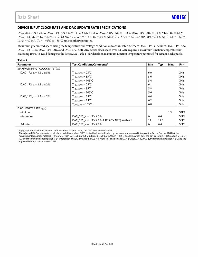
DEVICE INPUT CLOCK RATE AND DAC UPDATE RATE SPECIFICATIONS DAC_2P5_AN = 2.5 V, DAC_1P2_AN = DAC_1P2_CLK = 1.2 V, DAC_N1P2_AN = −1.2 V, DAC_1P2_DIG = 1.2 V, VDD_IO = 2.5 V, DAC_1P2_SER = 1.2 V, DAC_3P3_SYNC = 3.3 V, AMP_5V_IN = 5.0 V, AMP_3P3_OUT = 3.3 V, AMP_3P3 = 3.3 V, AMP_N5 = −5.0 V, IOUTFS = 40 mA, TA = −40°C to +85°C, unless otherwise noted.
Maximum guaranteed speed using the temperature and voltage conditions shown in Table 3, where DAC_1P2_x includes DAC_1P2_AN, DAC_1P2_CLK, DAC_1P2_DIG, and DAC_1P2_SER. Any device clock speed over 5.1 GHz requires a maximum junction temperature not exceeding 105°C to avoid damage to the device. See Table 11 for details on maximum junction temperature permitted for certain clock speeds.
Table 3. Parameter Test Conditions/Comments1 Min Typ Max Unit MAXIMUM INPUT CLOCK RATE (fCLK)
DAC_1P2_x = 1.2 V ± 5% TJ_DAC_MAX = 25°C 6.0 GHz TJ_DAC_MAX = 85°C 5.6 GHz TJ_DAC_MAX = 105°C 5.4 GHz DAC_1P2_x = 1.2 V ± 2% TJ_DAC_MAX = 25°C 6.1 GHz TJ_DAC_MAX = 85°C 5.8 GHz TJ_DAC_MAX = 105°C 5.6 GHz DAC_1P2_x = 1.3 V ± 2% TJ_DAC_MAX = 25°C 6.4 GHz TJ_DAC_MAX = 85°C 6.2 GHz T_DAC_MAX = 105°C 6.0 GHz
DAC UPDATE RATE (fDAC) Minimum 1.5 GSPS Maximum DAC_1P2_x = 1.3 V ± 2% 6 6.4 GSPS DAC_1P2_x = 1.3 V ± 2%, FIR85 (2× NRZ) enabled 12 12.8 GSPS Adjusted2 DAC_1P2_x = 1.3 V ± 2% 6 6.4 GSPS
1 TJ_DAC_MAX is the maximum junction temperature measured using the DAC temperature sensor. 2 The adjusted DAC update rate is calculated as follows: when FIR85 is disabled, fDAC is divided by the minimum required interpolation factor. For the AD9166, the
minimum interpolation factor is 1. Therefore, with fDAC = 6.0 GSPS, fDAC adjusted = 6.0 GSPS. When FIR85 is enabled, which puts the device into 2× NRZ mode, fDAC = 2 × fCLK, and the minimum interpolation is 2× (interpolation value). Thus, for the AD9166, with FIR85 enabled and fCLK = 6 GHz, fDAC = 12.0 GSPS, minimum interpolation = 2×, and the adjusted DAC update rate = 6.0 GSPS.
AD9166 Data Sheet
Rev. 0 | Page 8 of 138
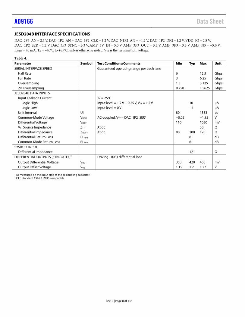
JESD204B INTERFACE SPECIFICATIONS DAC_2P5_AN = 2.5 V, DAC_1P2_AN = DAC_1P2_CLK = 1.2 V, DAC_N1P2_AN = −1.2 V, DAC_1P2_DIG = 1.2 V, VDD_IO = 2.5 V, DAC_1P2_SER = 1.2 V, DAC_3P3_SYNC = 3.3 V, AMP_5V_IN = 5.0 V, AMP_3P3_OUT = 3.3 V, AMP_3P3 = 3.3 V, AMP_N5 = −5.0 V, IOUTFS = 40 mA, TA = −40°C to +85°C, unless otherwise noted. VTT is the termination voltage.
Table 4. Parameter Symbol Test Conditions/Comments Min Typ Max Unit SERIAL INTERFACE SPEED Guaranteed operating range per each lane
Half Rate 6 12.5 Gbps Full Rate 3 6.25 Gbps Oversampling 1.5 3.125 Gbps 2× Oversampling 0.750 1.5625 Gbps
JESD204B DATA INPUTS
Input Leakage Current TA = 25°C
Logic High Input level = 1.2 V ± 0.25 V, VTT = 1.2 V 10 μA Logic Low Input level = 0 V −4 μA
Unit Interval UI 80 1333 ps Common-Mode Voltage VRCM AC-coupled, VTT = DAC_1P2_SER1 −0.05 +1.85 V Differential Voltage VDIFF 110 1050 mV VTT Source Impedance ZTT At dc 30 Ω Differential Impedance ZRDIFF At dc 80 100 120 Ω Differential Return Loss RLRDIF 8 dB Common-Mode Return Loss RLRCM 6 dB
SYSREF± INPUT Differential Impedance 121 Ω
DIFFERENTIAL OUTPUTS (SYNCOUT±)2 Driving 100 Ω differential load
Output Differential Voltage VOD 350 420 450 mV Output Offset Voltage VOS 1.15 1.2 1.27 V
1 As measured on the input side of the ac coupling capacitor. 2 IEEE Standard 1596.3 LVDS compatible.
Data Sheet AD9166
Rev. 0 | Page 9 of 138
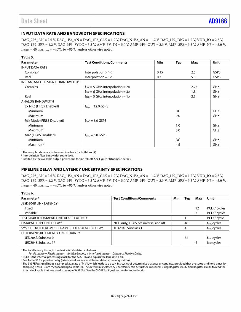
INPUT DATA RATE AND BANDWIDTH SPECIFICATIONS DAC_2P5_AN = 2.5 V, DAC_1P2_AN = DAC_1P2_CLK = 1.2 V, DAC_N1P2_AN = −1.2 V, DAC_1P2_DIG = 1.2 V, VDD_IO = 2.5 V, DAC_1P2_SER = 1.2 V, DAC_3P3_SYNC = 3.3 V, AMP_5V_IN = 5.0 V, AMP_3P3_OUT = 3.3 V, AMP_3P3 = 3.3 V, AMP_N5 = −5.0 V, IOUTFS = 40 mA, TA = −40°C to +85°C, unless otherwise noted.
Table 5. Parameter Test Conditions/Comments Min Typ Max Unit INPUT DATA RATE
Complex1 Interpolation > 1× 0.15 2.5 GSPS Real Interpolation = 1× 0.3 5.0 GSPS
INSTANTANEOUS SIGNAL BANDWIDTH2 Complex fCLK = 5 GHz, interpolation = 2× 2.25 GHz
fCLK = 6 GHz, interpolation = 3× 1.8 GHz Real fCLK = 5 GHz, interpolation = 1× 2.5 GHz
ANALOG BANDWIDTH 2x NRZ (FIR85 Enabled) fDAC = 12.0 GSPS
Minimum DC GHz Maximum 9.0 GHz
Mix Mode (FIR85 Disabled) fDAC = 6.0 GSPS Minimum 1.0 GHz Maximum 8.0 GHz
NRZ (FIR85 Disabled) fDAC = 6.0 GSPS Minimum DC GHz Maximum3 4.5 GHz
1 The complex data rate is the combined rate for both I and Q. 2 Interpolation filter bandwidth set to 90%. 3 Limited by the available output power due to sinc roll-off. See Figure 88 for more details.
PIPELINE DELAY AND LATENCY UNCERTAINTY SPECIFICATIONS DAC_2P5_AN = 2.5 V, DAC_1P2_AN = DAC_1P2_CLK = 1.2 V, DAC_N1P2_AN = −1.2 V, DAC_1P2_DIG = 1.2 V, VDD_IO = 2.5 V, DAC_1P2_SER = 1.2 V, DAC_3P3_SYNC = 3.3 V, AMP_5V_IN = 5.0 V, AMP_3P3_OUT = 3.3 V, AMP_3P3 = 3.3 V, AMP_N5 = −5.0 V, IOUTFS = 40 mA, TA = −40°C to +85°C, unless otherwise noted.
Table 6. Parameter1 Test Conditions/Comments Min Typ Max Unit JESD204B LINK LATENCY
Fixed 12 PCLK2 cycles Variable 2 PCLK2 cycles
JESD204B TO DATAPATH INTERFACE LATENCY 1 PCLK2 cycle DATAPATH PIPELINE DELAY3 NCO only, FIR85 off, inverse sinc off 48 fCLK cycles SYSREF± to LOCAL MULTIFRAME CLOCKS (LMFC) DELAY JED204B Subclass 1 4 fCLK cycles
DETERMINISTIC LATENCY UNCERTAINTY JED204B Subclass 0 32 fCLK cycles JED204B Subclass 14 4 fCLK cycles
1 The total latency through the device is calculated as follows:
Total Latency = Fixed Latency + Variable Latency + Interface Latency + Datapath Pipeline Delay. 2 PCLK is the internal processing clock for the AD9166 and equals the lane rate ÷ 40. 3 See Table 33 for pipeline delay (latency) values across different datapath configurations. 4 The SYSREF± signal input is sampled at a rate of fCLK/4, which leads to up to 4 fCLK cycles of deterministic latency uncertainty, provided that the setup and hold times for
sampling SYSREF± are met according to Table 10. The deterministic latency uncertainty can be further improved, using Register 0x037 and Register 0x038 to read the exact clock cycle that was used to sample SYSREF±. See the SYSREF± Signal section for more details.
AD9166 Data Sheet
Rev. 0 | Page 10 of 138
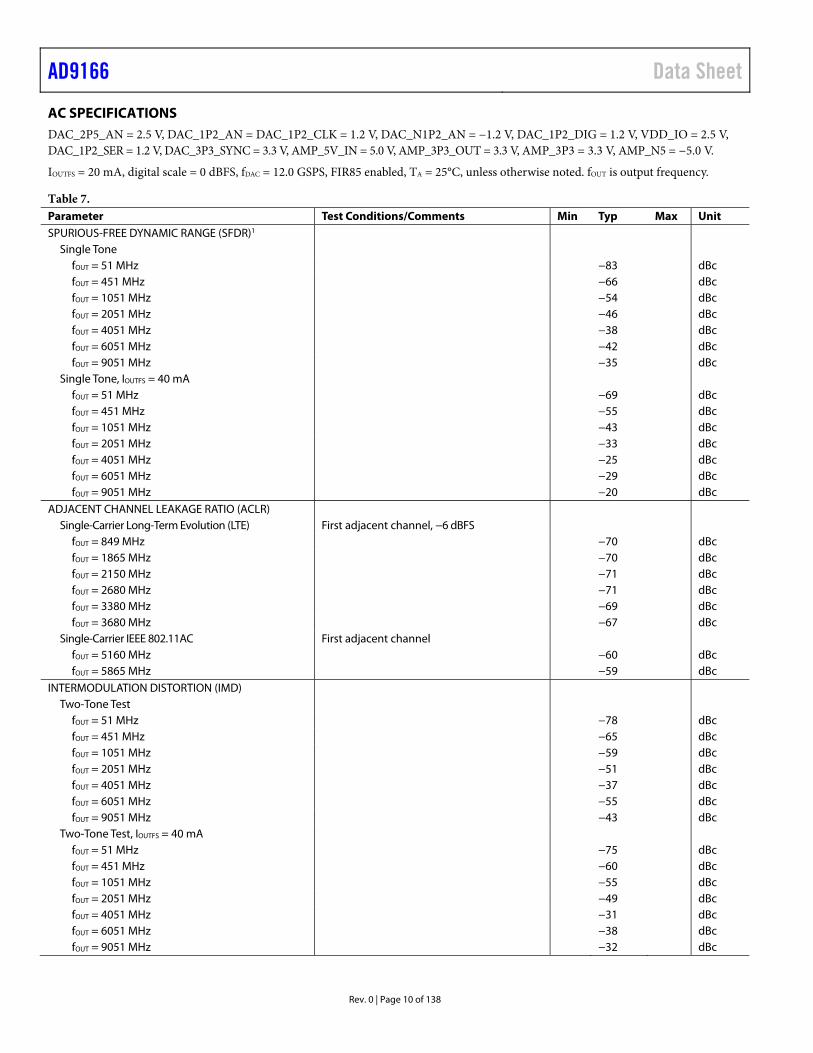
AC SPECIFICATIONS DAC_2P5_AN = 2.5 V, DAC_1P2_AN = DAC_1P2_CLK = 1.2 V, DAC_N1P2_AN = −1.2 V, DAC_1P2_DIG = 1.2 V, VDD_IO = 2.5 V, DAC_1P2_SER = 1.2 V, DAC_3P3_SYNC = 3.3 V, AMP_5V_IN = 5.0 V, AMP_3P3_OUT = 3.3 V, AMP_3P3 = 3.3 V, AMP_N5 = −5.0 V.
IOUTFS = 20 mA, digital scale = 0 dBFS, fDAC = 12.0 GSPS, FIR85 enabled, TA = 25°C, unless otherwise noted. fOUT is output frequency.
Table 7. Parameter Test Conditions/Comments Min Typ Max Unit SPURIOUS-FREE DYNAMIC RANGE (SFDR)1
Single Tone fOUT = 51 MHz −83 dBc fOUT = 451 MHz −66 dBc fOUT = 1051 MHz −54 dBc fOUT = 2051 MHz −46 dBc fOUT = 4051 MHz −38 dBc fOUT = 6051 MHz −42 dBc fOUT = 9051 MHz −35 dBc
Single Tone, IOUTFS = 40 mA fOUT = 51 MHz −69 dBc fOUT = 451 MHz −55 dBc fOUT = 1051 MHz −43 dBc fOUT = 2051 MHz −33 dBc fOUT = 4051 MHz −25 dBc fOUT = 6051 MHz −29 dBc fOUT = 9051 MHz −20 dBc
ADJACENT CHANNEL LEAKAGE RATIO (ACLR) Single-Carrier Long-Term Evolution (LTE) First adjacent channel, −6 dBFS
fOUT = 849 MHz −70 dBc fOUT = 1865 MHz −70 dBc fOUT = 2150 MHz −71 dBc fOUT = 2680 MHz −71 dBc fOUT = 3380 MHz −69 dBc fOUT = 3680 MHz −67 dBc
Single-Carrier IEEE 802.11AC First adjacent channel fOUT = 5160 MHz −60 dBc fOUT = 5865 MHz −59 dBc
INTERMODULATION DISTORTION (IMD) Two-Tone Test
fOUT = 51 MHz −78 dBc fOUT = 451 MHz −65 dBc fOUT = 1051 MHz −59 dBc fOUT = 2051 MHz −51 dBc fOUT = 4051 MHz −37 dBc fOUT = 6051 MHz −55 dBc fOUT = 9051 MHz −43 dBc
Two-Tone Test, IOUTFS = 40 mA fOUT = 51 MHz −75 dBc fOUT = 451 MHz −60 dBc fOUT = 1051 MHz −55 dBc fOUT = 2051 MHz −49 dBc fOUT = 4051 MHz −31 dBc fOUT = 6051 MHz −38 dBc fOUT = 9051 MHz −32 dBc
Data Sheet AD9166
Rev. 0 | Page 11 of 138
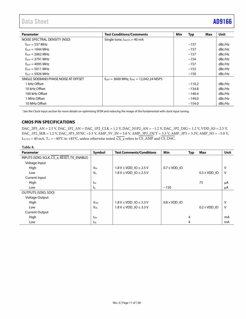
Parameter Test Conditions/Comments Min Typ Max Unit NOISE SPECTRAL DENSITY (NSD) Single tone, IOUTFS = 40 mA
fOUT = 537 MHz −157 dBc/Hz fOUT = 1044 MHz −157 dBc/Hz fOUT = 2062 MHz −157 dBc/Hz fOUT = 3791 MHz −154 dBc/Hz fOUT = 4095 MHz −157 dBc/Hz fOUT = 5011 MHz −153 dBc/Hz fOUT = 5926 MHz −150 dBc/Hz
SINGLE SIDEBAND PHASE NOISE AT OFFSET fOUT = 3600 MHz, fDAC = 12,042.24 MSPS 1 kHz Offset −110.2 dBc/Hz 10 kHz Offset −134.8 dBc/Hz 100 kHz Offset −140.4 dBc/Hz 1 MHz Offset −149.0 dBc/Hz 10 MHz Offset −154.0 dBc/Hz
1 See the Clock Input section for more details on optimizing SFDR and reducing the image of the fundamental with clock input tuning.
CMOS PIN SPECIFICATIONS DAC_2P5_AN = 2.5 V, DAC_1P2_AN = DAC_1P2_CLK = 1.2 V, DAC_N1P2_AN = −1.2 V, DAC_1P2_DIG = 1.2 V, VDD_IO = 2.5 V, DAC_1P2_SER = 1.2 V, DAC_3P3_SYNC =3.3 V, AMP_5V_IN = 5.0 V, AMP_3P3_OUT = 3.3 V, AMP_3P3 = 3.3V, AMP_N5 = −5.0 V, IOUTFS = 40 mA, TA = −40°C to +85°C, unless otherwise noted. CS_x refers to CS_AMP and CS_DAC.
Table 8. Parameter Symbol Test Comments/Conditions Min Typ Max Unit INPUTS (SDIO, SCLK, CS_x, RESET, TX_ENABLE)
Voltage Input High VIH 1.8 V ≤ VDD_IO ≤ 2.5 V 0.7 × VDD_IO V Low VIL 1.8 V ≤ VDD_IO ≤ 2.5 V 0.3 × VDD_IO V
Current Input High IIH 75 μA Low IIL −150 μA
OUTPUTS (SDIO, SDO) Voltage Output
High VOH 1.8 V ≤ VDD_IO ≤ 3.3 V 0.8 × VDD_IO V Low VOL 1.8 V ≤ VDD_IO ≤ 3.3 V 0.2 × VDD_IO V
Current Output High IOH 4 mA Low IOL 4 mA
AD9166 Data Sheet
Rev. 0 | Page 12 of 138
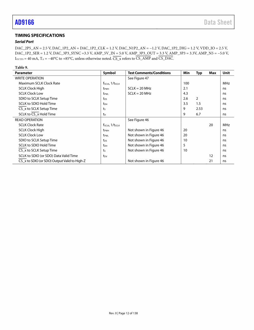
TIMING SPECIFICATIONS Serial Port
DAC_2P5_AN = 2.5 V, DAC_1P2_AN = DAC_1P2_CLK = 1.2 V, DAC_N1P2_AN = −1.2 V, DAC_1P2_DIG = 1.2 V, VDD_IO = 2.5 V, DAC_1P2_SER = 1.2 V, DAC_3P3_SYNC =3.3 V, AMP_5V_IN = 5.0 V, AMP_3P3_OUT = 3.3 V, AMP_3P3 = 3.3V, AMP_N5 = −5.0 V, IOUTFS = 40 mA, TA = −40°C to +85°C, unless otherwise noted. CS_x refers to CS_AMP and CS_DAC.
Table 9. Parameter Symbol Test Comments/Conditions Min Typ Max Unit WRITE OPERATION See Figure 47
Maximum SCLK Clock Rate fSCLK, 1/tSCLK 100 MHz SCLK Clock High tPWH SCLK = 20 MHz 2.1 ns SCLK Clock Low tPWL SCLK = 20 MHz 4.3 ns SDIO to SCLK Setup Time tDS 2.6 2 ns SCLK to SDIO Hold Time tDH 3.5 1.5 ns CS_x to SCLK Setup Time tS 9 2.53 ns
SCLK to CS_x Hold Time tH 9 6.7 ns
READ OPERATION See Figure 46 SCLK Clock Rate fSCLK, 1/tSCLK 20 MHz SCLK Clock High tPWH Not shown in Figure 46 20 ns SCLK Clock Low tPWL Not shown in Figure 46 20 ns SDIO to SCLK Setup Time tDS Not shown in Figure 46 10 ns SCLK to SDIO Hold Time tDH Not shown in Figure 46 5 ns CS_x to SCLK Setup Time tS Not shown in Figure 46 10 ns
SCLK to SDIO (or SDO) Data Valid Time tDV 12 ns CS_x to SDIO (or SDO) Output Valid to High-Z Not shown in Figure 46 21 ns
Data Sheet AD9166
Rev. 0 | Page 13 of 138
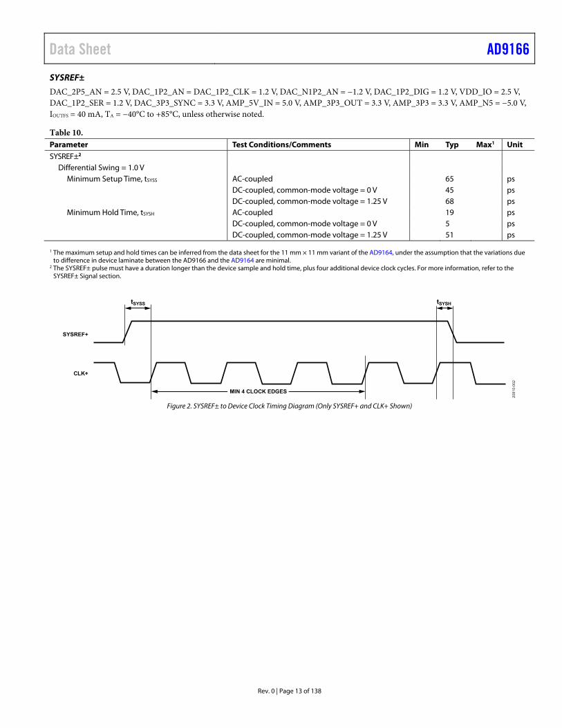
SYSREF±
DAC_2P5_AN = 2.5 V, DAC_1P2_AN = DAC_1P2_CLK = 1.2 V, DAC_N1P2_AN = −1.2 V, DAC_1P2_DIG = 1.2 V, VDD_IO = 2.5 V, DAC_1P2_SER = 1.2 V, DAC_3P3_SYNC = 3.3 V, AMP_5V_IN = 5.0 V, AMP_3P3_OUT = 3.3 V, AMP_3P3 = 3.3 V, AMP_N5 = −5.0 V, IOUTFS = 40 mA, TA = −40°C to +85°C, unless otherwise noted.
Table 10. Parameter Test Conditions/Comments Min Typ Max1 Unit SYSREF±2
Differential Swing = 1.0 V Minimum Setup Time, tSYSS AC-coupled 65 ps DC-coupled, common-mode voltage = 0 V 45 ps
DC-coupled, common-mode voltage = 1.25 V 68 ps Minimum Hold Time, tSYSH AC-coupled 19 ps DC-coupled, common-mode voltage = 0 V 5 ps
DC-coupled, common-mode voltage = 1.25 V 51 ps 1 The maximum setup and hold times can be inferred from the data sheet for the 11 mm × 11 mm variant of the AD9164, under the assumption that the variations due
to difference in device laminate between the AD9166 and the AD9164 are minimal. 2 The SYSREF± pulse must have a duration longer than the device sample and hold time, plus four additional device clock cycles. For more information, refer to the
SYSREF± Signal section.
SYSREF+
tSYSS
CLK+
tSYSH
MIN 4 CLOCK EDGES
2081
0-00
2
Figure 2. SYSREF± to Device Clock Timing Diagram (Only SYSREF+ and CLK+ Shown)
AD9166 Data Sheet
Rev. 0 | Page 14 of 138
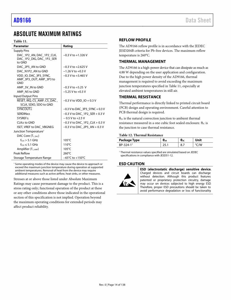
ABSOLUTE MAXIMUM RATINGS Table 11. Parameter Rating Supply Pins
DAC_1P2_AN, DAC_1P2_CLK, DAC_1P2_DIG, DAC_1P2_SER to GND
−0.3 V to +1.326 V
DAC_2P5_AN to GND −0.3 V to +2.625 V DAC_N1P2_AN to GND −1.26 V to +0.3 V VDD_IO, DAC_3P3_SYNC, AMP_3P3_OUT, AMP_3P3 to GND
−0.3 V to +3.465 V
AMP_5V_IN to GND −0.3 V to +5.25 V AMP_N5 to GND −5.25 V to +0.3 V
Input/Output Pins RESET, IRQ, CS_AMP, CS_DAC ,
SCLK, SDIO, SDO to GND −0.3 V to VDD_IO + 0.3 V
SYNCOUT± −0.3 V to DAC_3P3_SYNC + 0.3 V
SERDINx± −0.3 V to DAC_1P2_SER + 0.3 V SYSREF± − 0.5 V to +2.5 V CLK± to GND −0.3 V to DAC_1P2_CLK + 0.3 V ISET, VREF to DAC_VBGNEG −0.3 V to DAC_2P5_AN + 0.3 V
Junction Temperature1 DAC Core (TJ_DAC)
fCLK > 5.1 GHz 105°C fCLK ≤ 5.1 GHz 110°C
Amplifier (TJ_AMP) 105°C Peak Reflow 260°C Storage Temperature Range −65°C to +150°C
1 Some operating modes of the device may cause the device to approach or exceed the maximum junction temperature during operation at supported ambient temperatures. Removal of heat from the device may require additional measures such as active airflow, heat sinks, or other measures.
Stresses at or above those listed under Absolute Maximum Ratings may cause permanent damage to the product. This is a stress rating only; functional operation of the product at these or any other conditions above those indicated in the operational section of this specification is not implied. Operation beyond the maximum operating conditions for extended periods may affect product reliability.
REFLOW PROFILE The AD9166 reflow profile is in accordance with the JEDEC JESD204B criteria for Pb-free devices. The maximum reflow temperature is 260°C.
THERMAL MANAGEMENT The AD9166 is a high-power device that can dissipate as much as 4.88 W depending on the user application and configuration. Due to the high power density of the AD9166, thermal management is required to avoid exceeding the maximum junction temperatures specified in Table 11, especially at elevated ambient temperatures in still air.
THERMAL RESISTANCE Thermal performance is directly linked to printed circuit board (PCB) design and operating environment. Careful attention to PCB thermal design is required.
θJA is the natural convection junction to ambient thermal resistance measured in a one cubic foot sealed enclosure. θJC is the junction to case thermal resistance.
Table 12. Thermal Resistance Package Type θJA θJC Unit BP-324-11 25.1 8.7 °C/W 1 Thermal resistance values specified are simulated based on JEDEC
specifications in compliance with JESD51-12.
ESD CAUTION
Data Sheet AD9166
Rev. 0 | Page 15 of 138
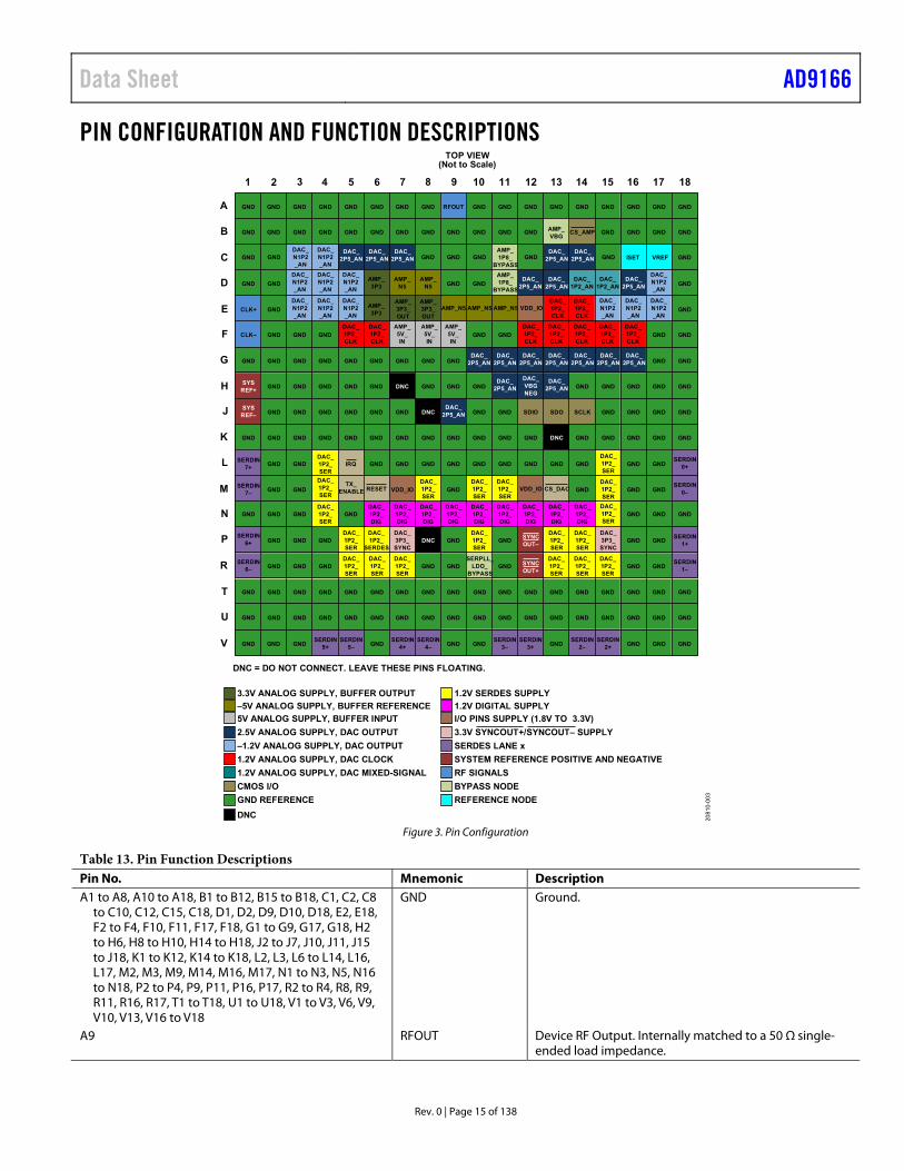
PIN CONFIGURATION AND FUNCTION DESCRIPTIONS
A
B
C
D
E
F
G
H
J
K
L
M
N
P
R
T
U
V
DNC = DO NOT CONNECT. LEAVE THESE PINS FLOATING.
3.3V ANALOG SUPPLY, BUFFER OUTPUT–5V ANALOG SUPPLY, BUFFER REFERENCE5V ANALOG SUPPLY, BUFFER INPUT2.5V ANALOG SUPPLY, DAC OUTPUT–1.2V ANALOG SUPPLY, DAC OUTPUT1.2V ANALOG SUPPLY, DAC CLOCK1.2V ANALOG SUPPLY, DAC MIXED-SIGNALCMOS I/OGND REFERENCEDNC
1.2V SERDES SUPPLY1.2V DIGITAL SUPPLYI/O PINS SUPPLY (1.8V TO 3.3V)3.3V SYNCOUT+/SYNCOUT– SUPPLYSERDES LANE xSYSTEM REFERENCE POSITIVE AND NEGATIVERF SIGNALSBYPASS NODEREFERENCE NODE
1 2 3 4 5 6 7 8 9 10 11 12 13 14 15 16 17 18
TOP VIEW(Not to Scale)
GND GNDGND
GND
GND
GND
GND
GND GND GND GND GND RFOUT GND GND GND GND GND GND GND GND
GND GND GND GND GND GND GND GND GND GND GND AMP_VBG CS_AMP GND GND GND
GND GND GND GND GND GND GND GND
GND GNDGNDGND GND GND GND GND GND GND GND GND GND GND GND GND GND
GNDGND GNDDAC_1P2_SER
DAC_1P2_SER
DAC_1P2_SER
GND GNDSERPLL_
LDO_BYPASS
GNDDAC_1P2_SER
DAC_1P2_SER
DAC_1P2_SER
GND GND
GND GNDGNDGND GND GND GND GND GND GND
GND
GND GND GND GND GND GND GND GND
GND
GND GNDGNDAMP_3P3
AMP_3P3
AMP_N5
AMP_N5
AMP_3P3_OUT
AMP_3P3_OUT
GNDGND
CLK+ GNDAMP_N5 AMP_N5 AMP_N5 VDD_IOGND
CLK– GNDGNDAMP_5V_IN
AMP_5V_IN
AMP_5V_IN
GND GND GNDGND GND
GND GNDGND GND GND GNDGND GND GNDGND GND
SYSREF+
SYSREF–
GNDGND DNC GND GNDGND GND GND GNDDAC_VBGNEG
GND GND GNDGND GND
GNDGND GND DNCDAC_
2P5_ANGND GND GND GND GND SDIO SDO SCLK GND GNDGND GND
GND GNDGND GND GND GNDGND GND GND GND GND GND DNC GND GND GNDGND GND
SERDIN7+
SERDIN7–
SERDIN0+
SERDIN0–
SERDIN1+
SERDIN1–
SERDIN6–
SERDIN5+
SERDIN5–
SERDIN4+
SERDIN4–
SERDIN3–
SERDIN3+
SERDIN2–
SERDIN2+
SERDIN6+
GND GND GND GNDDAC_1P2_SER
IRQ GND GND GND GND GND GNDDAC_1P2_SER
GNDGND GND
GND VDD_IODAC_1P2_SER
GNDDAC_1P2_SER
RESETTX_
ENABLEDAC_1P2_SER
DAC_1P2_SER
VDD_IO CS_DAC GNDDAC_1P2_SER
GNDGND GND
GND GND
2081
0-00
3
GNDDAC_1P2_DIG
DAC_1P2_DIG
DAC_1P2_DIG
DAC_1P2_SER
GNDDAC_1P2_DIG
DAC_1P2_DIG
DAC_1P2_DIG
DAC_1P2_DIG
DAC_1P2_DIG
DAC_1P2_DIG
DAC_1P2_SER
GNDGND GND
GNDDAC_3P3_SYNC
DAC_3P3_SYNC
DNC GNDGNDDAC_1P2_SER
DAC_1P2_
SERDES
DAC_1P2_SER
GND SYNCOUT–
SYNCOUT+
DAC_1P2_SER
DAC_1P2_SER
GNDGND GND
GND GNDDAC_N1P2_AN
DAC_2P5_AN
DAC_2P5_AN
DAC_2P5_AN
DAC_2P5_AN
DAC_2P5_AN
DAC_2P5_AN
DAC_2P5_AN
DAC_2P5_AN
DAC_2P5_AN
DAC_2P5_AN
DAC_2P5_AN
DAC_2P5_AN
DAC_2P5_AN
DAC_2P5_AN
DAC_2P5_AN
DAC_2P5_AN
DAC_1P2_AN
DAC_1P2_CLK
DAC_1P2_CLK
DAC_1P2_CLK
DAC_1P2_CLK
DAC_1P2_CLK
DAC_1P2_CLK
DAC_1P2_CLK
DAC_1P2_AN
DAC_2P5_AN
DAC_N1P2_AN
DAC_N1P2_AN
DAC_N1P2_AN
DAC_N1P2_AN
DAC_N1P2_AN
DAC_N1P2_AN
DAC_N1P2_AN
DAC_N1P2_AN
DAC_N1P2_AN
DAC_N1P2_AN
DAC_N1P2_AN
DAC_1P2_CLK
DAC_1P2_CLK
GND GND ISET VREFGNDGNDAMP_1P8_
BYPASSAMP_1P8_
BYPASS
GNDGND
Figure 3. Pin Configuration
Table 13. Pin Function Descriptions Pin No. Mnemonic Description A1 to A8, A10 to A18, B1 to B12, B15 to B18, C1, C2, C8
to C10, C12, C15, C18, D1, D2, D9, D10, D18, E2, E18, F2 to F4, F10, F11, F17, F18, G1 to G9, G17, G18, H2 to H6, H8 to H10, H14 to H18, J2 to J7, J10, J11, J15 to J18, K1 to K12, K14 to K18, L2, L3, L6 to L14, L16, L17, M2, M3, M9, M14, M16, M17, N1 to N3, N5, N16 to N18, P2 to P4, P9, P11, P16, P17, R2 to R4, R8, R9, R11, R16, R17, T1 to T18, U1 to U18, V1 to V3, V6, V9, V10, V13, V16 to V18
GND Ground.
A9 RFOUT Device RF Output. Internally matched to a 50 Ω single-ended load impedance.
AD9166 Data Sheet
Rev. 0 | Page 16 of 138
Pin No. Mnemonic Description B13 AMP_VBG Amplifier Band Gap Voltage. Connect Pin B13 to a 0.1 μF
capacitor to ground, and a 1 kΩ resistor in series with a 1 μF capacitor to ground. For information about the voltage measured at this pin, VBGA, see the Amplifier Junction Temperature Sensor section.
B14 CS_AMP Amplifier Serial Port Chip Select (Active Low) Input. CMOS levels on Pin B14 are determined with respect to VDD_IO.
C3, C4, D3 to D5, D17, E3 to E5, E15 to E17 DAC_N1P2_AN −1.2 V Analog Supply Voltage. C5 to C7, C13, C14, D12, D13, D16, G10 to G16, H11,
H13, J9 DAC_2P5_AN 2.5 V Analog Supply Voltage.
C11, D11 AMP_1P8_BYPASS Bypass Node for Internal1.8 V Analog Supply. Short Pin C11 and Pin D11 and connect a 1 μF capacitor to ground.
C16 ISET DAC Reference Current. Connect Pin C16 with a 9.76 kΩ resistor (RSET) to DAC_N1P2_AN.
C17 VREF DAC 1.2 V Reference Input/Output. Connect Pin C17 with a 1 μF capacitor to ground.
D6, E6 AMP_3P3 3.3 V Analog Supply Voltage. D7, D8, E9, E10, E11 AMP_N5 −5 V Analog Supply Voltage. D14, D15 DAC_1P2_AN 1.2 V Analog Supply Voltage. E1, F1 CLK+, CLK− Positive and Negative Device Clock Inputs. When FIR85 is
disabled, the input frequency to these pins (fCLK) is the DAC clock frequency (fDAC). When FIR85 is enabled, fDAC = 2× fCLK.
E7, E8 AMP_3P3_OUT 3.3 V Analog Supply Voltage for the Output Stage of the Amplifier.
E12, M7, M12 VDD_IO Supply Voltage for CMOS Input/Output and SPI. Operational for 1.8 V to 3.3 V plus tolerance (see Table 1 for details).
E13, E14, F5, F6, F12 to F16 DAC_1P2_CLK 1.2 V Clock Supply Voltage. F7, F8, F9 AMP_5V_IN 5 V Analog Supply Voltage for the Input Stage of the
Amplifier. Pin F7 to Pin F9 internally supply the full-scale current to the output stage of the DAC.
H1, J1 SYSREF+, SYSREF− System Reference Positive and Negative Inputs. The H1 and J1 pins are self biased for ac coupling. They both can be either ac-coupled or dc-coupled.
H7, J8, K13, P8 DNC Do Not Connect. Do not connect these pins. Leave the DNC pins floating.
H12 DAC_VBGNEG DAC Band Gap Voltage. Connect Pin H12 with a 0.1 μF capacitor to DAC_N1P2_AN.
J12 SDIO Serial Port Data Input/Output. CMOS levels on Pin J12 are determined with respect to VDD_IO. See the Serial Data I/O (SDIO) section for details.
J13 SDO Serial Port Data Output. CMOS levels on Pin J13 are determined with respect to VDD_IO.
J14 SCLK Serial Port Data Clock. CMOS levels on Pin J14 are determined with respect to VDD_IO. See the Serial Clock (SCLK) section for details.
L1, M1 SERDIN7+, SERDIN7− SERDES Lane 7 Negative and Positive Inputs. L4, L15, M4, M8, M10, M11, M15, N4, N15, P5, P6, P10,
P13, P14, R5 to R7, R13 to R15 DAC_1P2_SER 1.2 V SERDES Digital Supply.
L5 IRQ Interrupt Request Output (Active Low, Open Drain).
L18, M18 SERDIN0+, SERDIN0− SERDES Lane 1 Positive and Negative Inputs. M5 TX_ENABLE Transmit Enable Input. Pin M5 can be used instead of the
DAC output bias power-down bits in Register 0x040, Bits[1:0], to enable the DAC output. CMOS levels are determined with respect to VDD_IO.
Data Sheet AD9166
Rev. 0 | Page 17 of 138
Pin No. Mnemonic Description M6 RESET Reset (Active Low) Input. CMOS levels on Pin M6 are
determined with respect to VDD_IO. M13 CS_DAC DAC Serial Port Chip Select (Active Low) Input. CMOS
levels on Pin M13 are determined with respect to VDD_IO.
N6 to N14 DAC_1P2_DIG 1.2 V Digital Supply Voltage for the Digital Signal Processing (DSP) Blocks of the DAC.
P1, R1 SERDIN6+, SERDIN6− SERDES Lane 6 Negative and Positive Inputs. P7, P15 DAC_3P3_SYNC 3.3 V SERDES Sync Supply Voltage. P12, R12 SYNCOUT−,
SYNCOUT+ Negative and Positive LVDS Sync (Active Low) Output Signals.
P18, R18 SERDIN1+, SERDIN1− SERDES Lane 1 Positive and Negative Inputs. R10 SERPLL_LDO_BYPASS SERDES PLL Supply Voltage Bypass. Connect this pin with
a 1 Ω resistor in series with a 1 μF capacitor to ground. V15, V14 SERDIN2+, SERDIN2− SERDES Lane 2 Positive and Negative Inputs. V12, V11 SERDIN3+, SERDIN3− SERDES Lane 3 Positive and Negative Inputs. V7, V8 SERDIN4+, SERDIN4− SERDES Lane 4 Negative and Positive Inputs. V4, V5 SERDIN5+, SERDIN5− SERDES Lane 5 Negative and Positive Inputs.
AD9166 Data Sheet
Rev. 0 | Page 18 of 138
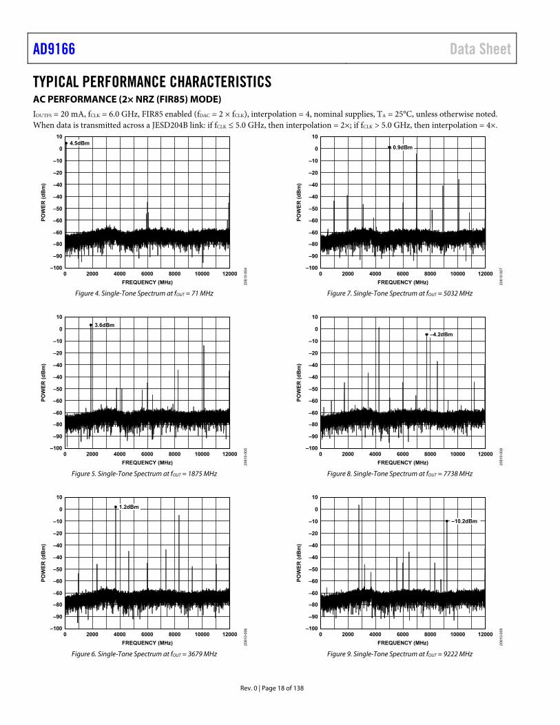
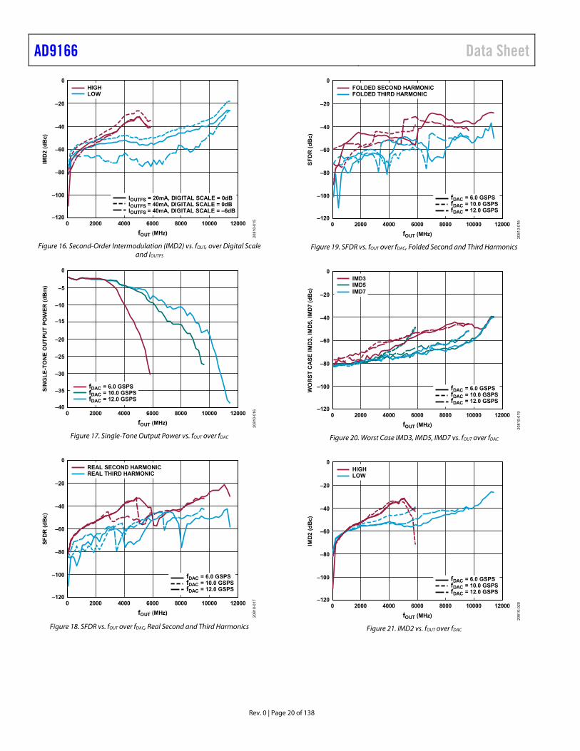
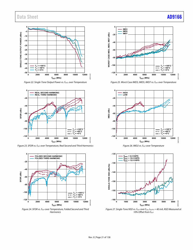
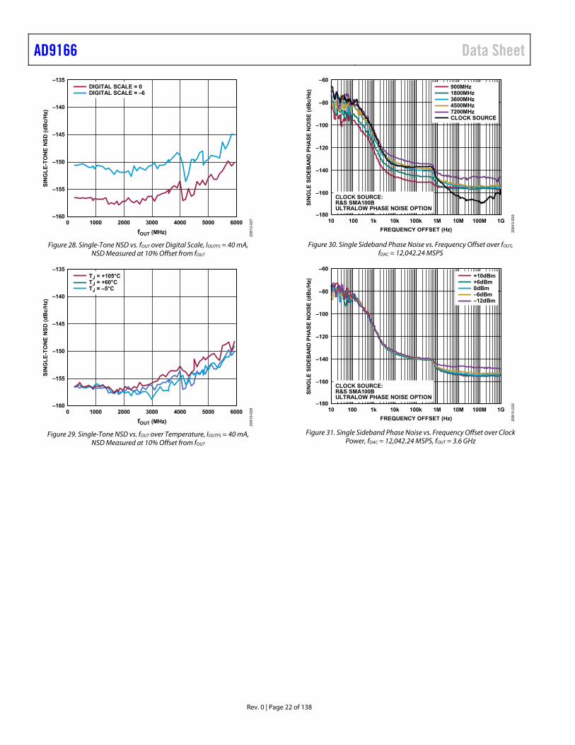
TYPICAL PERFORMANCE CHARACTERISTICS AC PERFORMANCE (2× NRZ (FIR85) MODE) IOUTFS = 20 mA, fCLK = 6.0 GHz, FIR85 enabled (fDAC = 2 × fCLK), interpolation = 4, nominal supplies, TA = 25°C, unless otherwise noted. When data is transmitted across a JESD204B link: if fCLK ≤ 5.0 GHz, then interpolation = 2×; if fCLK > 5.0 GHz, then interpolation = 4×.
0
10
–20
–40
–60
–80
–10
–40
–50
–60
–90
–100
POW
ER (d
Bm)
FREQUENCY (MHz)0 12000100008000600040002000
4.5dBm
2081
0-00
4
Figure 4. Single-Tone Spectrum at fOUT = 71 MHz
10
–20
–40
–60
–80
–10
–40
–50
–60
–90
–100
POW
ER (d
Bm)
FREQUENCY (MHz)0 12000100008000600040002000
03.6dBm
2081
0-00
5
Figure 5. Single-Tone Spectrum at fOUT = 1875 MHz
1.2dBm10
–20
–40
–60
–80
–10
–40
–50
–60
–90
–100
POW
ER (d
Bm)
FREQUENCY (MHz)0 12000100008000600040002000
0
2081
0-00
6
Figure 6. Single-Tone Spectrum at fOUT = 3679 MHz
0.9dBm
10
–20
–40
–60
–80
–10
–40
–50
–60
–90
–100
POW
ER (d
Bm)
FREQUENCY (MHz)0 12000100008000600040002000
0
2081
0-00
7
Figure 7. Single-Tone Spectrum at fOUT = 5032 MHz
–4.2dBm
10
–20
–40
–60
–80
–10
–40
–50
–60
–90
–100
POW
ER (d
Bm)
FREQUENCY (MHz)0 12000100008000600040002000
0
2081
0-00
8
Figure 8. Single-Tone Spectrum at fOUT = 7738 MHz
–10.2dBm
10
–20
–40
–60
–80
–10
–40
–50
–60
–90
–100
POW
ER (d
Bm)
FREQUENCY (MHz)0 12000100008000600040002000
020
810-
009
Figure 9. Single-Tone Spectrum at fOUT = 9222 MHz
Data Sheet AD9166
Rev. 0 | Page 19 of 138
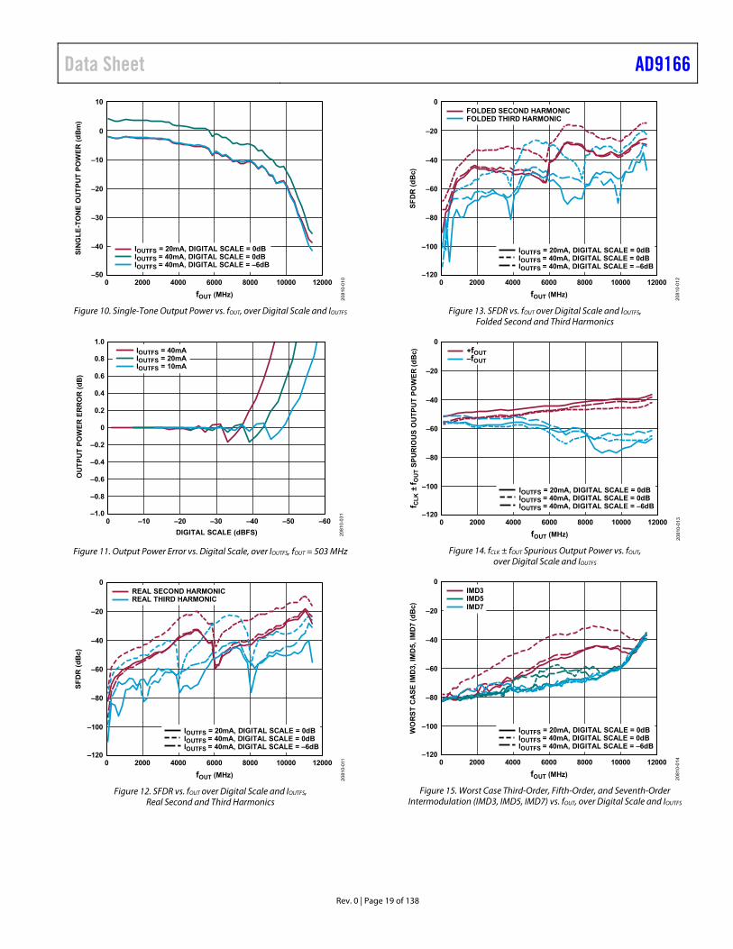
10
0
–10
–20
–30
–50
–40
0 12000100008000600040002000
SING
LE-T
ONE
OUT
PUT
POW
ER (d
Bm)
fOUT (MHz)
IOUTFS = 40mA, DIGITAL SCALE = –6dBIOUTFS = 40mA, DIGITAL SCALE = 0dBIOUTFS = 20mA, DIGITAL SCALE = 0dB
2081
0-01
0
Figure 10. Single-Tone Output Power vs. fOUT, over Digital Scale and IOUTFS
1.0
0.8
0.6
0.4
0.2
0
–0.2
–0.4
–0.6
–0.8
–1.00 –10 –30 –40 –50–20 –60
OUT
PUT
POW
ER E
RRO
R (d
B)
DIGITAL SCALE (dBFS)
IOUTFS = 10mAIOUTFS = 20mAIOUTFS = 40mA
2081
0-03
1
Figure 11. Output Power Error vs. Digital Scale, over IOUTFS, fOUT = 503 MHz
0
–60
–20
–100
–80
–120
–40
0 12000100008000600040002000
SFDR
(dBc
)
fOUT (MHz)
REAL THIRD HARMONICREAL SECOND HARMONIC
2081
0-01
1
IOUTFS = 20mA, DIGITAL SCALE = 0dB
IOUTFS = 40mA, DIGITAL SCALE = –6dBIOUTFS = 40mA, DIGITAL SCALE = 0dB
Figure 12. SFDR vs. fOUT over Digital Scale and IOUTFS, Real Second and Third Harmonics
0
–60
–20
–100
–80
–120
–40
0 12000100008000600040002000
SFDR
(dBc
)
fOUT (MHz)
FOLDED THIRD HARMONICFOLDED SECOND HARMONIC
2081
0-01
2
IOUTFS = 20mA, DIGITAL SCALE = 0dB
IOUTFS = 40mA, DIGITAL SCALE = –6dBIOUTFS = 40mA, DIGITAL SCALE = 0dB
Figure 13. SFDR vs. fOUT over Digital Scale and IOUTFS, Folded Second and Third Harmonics
0
–60
–20
–100
–80
–120
–40
0 12000100008000600040002000
f CLK
±f O
UT S
PURI
OUS
OUT
PUT
POW
ER (d
Bc)
fOUT (MHz)
–fOUT+fOUT
2081
0-01
3
IOUTFS = 20mA, DIGITAL SCALE = 0dB
IOUTFS = 40mA, DIGITAL SCALE = –6dBIOUTFS = 40mA, DIGITAL SCALE = 0dB
Figure 14. fCLK ± fOUT Spurious Output Power vs. fOUT, over Digital Scale and IOUTFS
0
–60
–20
–100
–80
–120
–40
0 12000100008000600040002000
WO
RST
CASE
IMD3
, IM
D5, I
MD7
(dBc
)
fOUT (MHz)
IMD5IMD3
IMD7
2081
0-01
4
IOUTFS = 20mA, DIGITAL SCALE = 0dB
IOUTFS = 40mA, DIGITAL SCALE = –6dBIOUTFS = 40mA, DIGITAL SCALE = 0dB
Figure 15. Worst Case Third-Order, Fifth-Order, and Seventh-Order Intermodulation (IMD3, IMD5, IMD7) vs. fOUT, over Digital Scale and IOUTFS
AD9166 Data Sheet
Rev. 0 | Page 20 of 138
0
–60
–20
–100
–80
–120
–40
0 12000100008000600040002000
IMD2
(dBc
)
fOUT (MHz)
LOWHIGH
2081
0-01
5
IOUTFS = 20mA, DIGITAL SCALE = 0dB
IOUTFS = 40mA, DIGITAL SCALE = –6dBIOUTFS = 40mA, DIGITAL SCALE = 0dB
Figure 16. Second-Order Intermodulation (IMD2) vs. fOUT, over Digital Scale and IOUTFS
0
–5
–10
–20
–15
–25
–30
–35
–400 12000100008000600040002000
SING
LE-T
ONE
OUT
PUT
POW
ER (d
Bm)
fOUT (MHz)
2081
0-01
6
fDAC = 12.0 GSPSfDAC = 10.0 GSPSfDAC = 6.0 GSPS
Figure 17. Single-Tone Output Power vs. fOUT over fDAC
0
–60
–20
–100
–80
–120
–40
0 12000100008000600040002000
SFDR
(dBc
)
fOUT (MHz)
REAL THIRD HARMONICREAL SECOND HARMONIC
2081
0-01
7
fDAC = 12.0 GSPSfDAC = 10.0 GSPSfDAC = 6.0 GSPS
Figure 18. SFDR vs. fOUT over fDAC, Real Second and Third Harmonics
0
–60
–20
–100
–80
–120
–40
0 12000100008000600040002000
SFDR
(dBc
)
fOUT (MHz)
FOLDED THIRD HARMONICFOLDED SECOND HARMONIC
fDAC = 12.0 GSPSfDAC = 10.0 GSPSfDAC = 6.0 GSPS
2081
0-01
8
Figure 19. SFDR vs. fOUT over fDAC, Folded Second and Third Harmonics
0
–60
–20
–100
–80
–120
–40
0 12000100008000600040002000
WO
RST
CAS
E IM
D3, I
MD
5, IM
D7 (d
Bc)
fOUT (MHz)
IMD5IMD3
IMD7
2081
0-01
9
fDAC = 12.0 GSPSfDAC = 10.0 GSPSfDAC = 6.0 GSPS
Figure 20. Worst Case IMD3, IMD5, IMD7 vs. fOUT over fDAC
0
–60
–20
–100
–80
–120
–40
0 12000100008000600040002000
IMD2
(dB
c)
fOUT (MHz)
LOWHIGH
2081
0-02
0
fDAC = 12.0 GSPSfDAC = 10.0 GSPSfDAC = 6.0 GSPS
Figure 21. IMD2 vs. fOUT over fDAC
Data Sheet AD9166
Rev. 0 | Page 21 of 138
0
–5
–10
–20
–15
–25
–30
–35
–50
–45
–40
0 12000100008000600040002000
SIN
GLE
-TO
NE O
UTP
UT
POW
ER (d
Bm)
fOUT (MHz)
TJ = +5°CTJ = +60°CTJ = +105°C
2081
0-02
1
Figure 22. Single-Tone Output Power vs. fOUT, over Temperature
0
–60
–20
–100
–80
–120
–40
0 12000100008000600040002000
SFD
R (d
Bc)
fOUT (MHz)
REAL THIRD HARMONICREAL SECOND HARMONIC
TJ = +5°CTJ = +60°CTJ = +105°C
2081
0-02
2
Figure 23. SFDR vs. fOUT over Temperature, Real Second and Third Harmonics
0
–60
–20
–100
–80
–120
–40
0 12000100008000600040002000
SFDR
(dBc
)
fOUT (MHz) 2081
0-02
3
FOLDED THIRD HARMONICFOLDED SECOND HARMONIC
TJ = +5°CTJ = +60°CTJ = +105°C
Figure 24. SFDR vs. fOUT over Temperature, Folded Second and Third Harmonics
0
–60
–20
–100
–80
–120
–40
0 12000100008000600040002000
WO
RST
CA
SE IM
D3,
IMD5
, IM
D7 (d
Bc)
fOUT (MHz)
IMD5IMD3
IMD7
2081
0-02
4
TJ = +5°CTJ = +60°CTJ = +105°C
Figure 25. Worst Case IMD3, IMD5, IMD7 vs. fOUT over Temperature
0
–60
–20
–100
–80
–120
–40
0 12000100008000600040002000
IMD
2 (d
Bc)
fOUT (MHz)
LOWHIGH
2081
0-02
5
TJ = +5°CTJ = +60°CTJ = +105°C
Figure 26. IMD2 vs. fOUT over Temperature
–135
–140
–145
–150
–155
–1600 600050004000300020001000
SIN
GLE
-TO
NE N
SD (d
Bc/
Hz)
fOUT (MHz)
fDAC = 12.0 GSPSfDAC = 10.0 GSPSfDAC = 6.0 GSPS
2081
0-02
6
Figure 27. Single-Tone NSD vs. fOUT over fCLK, IOUTFS = 40 mA, NSD Measured at 10% Offset from fOUT
AD9166 Data Sheet
Rev. 0 | Page 22 of 138
–135
–140
–145
–150
–155
–1600 600050004000300020001000
SIN
GLE
-TO
NE N
SD (d
Bc/
Hz)
fOUT (MHz)
DIGITAL SCALE = –6DIGITAL SCALE = 0
2081
0-02
7Figure 28. Single-Tone NSD vs. fOUT over Digital Scale, IOUTFS = 40 mA,
NSD Measured at 10% Offset from fOUT
–135
–140
–145
–150
–155
–1600 600050004000300020001000
SING
LE-T
ON
E N
SD (d
Bc/H
z)
fOUT (MHz)
TJ = –5°CTJ = +60°CTJ = +105°C
2081
0-02
8
Figure 29. Single-Tone NSD vs. fOUT over Temperature, IOUTFS = 40 mA, NSD Measured at 10% Offset from fOUT
–60
–80
–100
–120
–140
–160
–18010 100 10k 100k 1M 10M 100M1k 1G
SING
LE S
IDEB
AND
PHAS
E NO
ISE
(dBc
/Hz)
FREQUENCY OFFSET (Hz)
3600MHz1800MHz900MHz
7200MHz4500MHz
CLOCK SOURCE
CLOCK SOURCE:R&S SMA100BULTRALOW PHASE NOISE OPTION
2081
0-02
9
Figure 30. Single Sideband Phase Noise vs. Frequency Offset over fOUT, fDAC = 12,042.24 MSPS
–60
–80
–100
–120
–140
–160
–18010 100 10k 100k 1M 10M 100M1k 1G
SING
LE S
IDEB
AND
PHAS
E NO
ISE
(dBc
/Hz)
FREQUENCY OFFSET (Hz)
0dBm+6dBm+10dBm
–12dBm–6dBm
CLOCK SOURCE:R&S SMA100BULTRALOW PHASE NOISE OPTION
2081
0-03
0
Figure 31. Single Sideband Phase Noise vs. Frequency Offset over Clock Power, fDAC = 12,042.24 MSPS, fOUT = 3.6 GHz
Data Sheet AD9166
Rev. 0 | Page 23 of 138
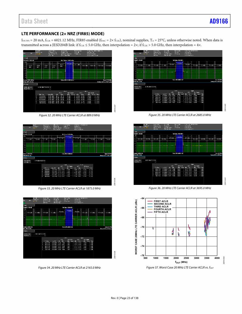
LTE PERFORMANCE (2× NRZ (FIR85) MODE) IOUTFS = 20 mA, fCLK = 6021.12 MHz, FIR85 enabled (fDAC = 2× fCLK), nominal supplies, TA = 25°C, unless otherwise noted. When data is transmitted across a JESD204B link: if fCLK ≤ 5.0 GHz, then interpolation = 2×; if fCLK > 5.0 GHz, then interpolation = 4×.
2081
0-03
7Figure 32. 20 MHz LTE Carrier ACLR at 889.0 MHz
2081
0-03
8
Figure 33. 20 MHz LTE Carrier ACLR at 1875.0 MHz
2081
0-03
9
Figure 34. 20 MHz LTE Carrier ACLR at 2165.0 MHz
2081
0-04
0
Figure 35. 20 MHz LTE Carrier ACLR at 2685.0 MHz
2081
0-04
1
Figure 36. 20 MHz LTE Carrier ACLR at 3695.0 MHz
–64
–70
–66
–74
–72
–76
–68
500 40003000 35002500200015001000
WO
RST
CASE
20M
Hz L
TE C
ARRI
ER A
CLR
(dBc
)
fOUT (MHz)
SECOND ACLRFIRST ACLR
THIRD ACLRFOURTH ACLRFIFTH ACLR
2081
0-04
2
Figure 37. Worst Case 20 MHz LTE Carrier ACLR vs. fOUT
AD9166 Data Sheet
Rev. 0 | Page 24 of 138
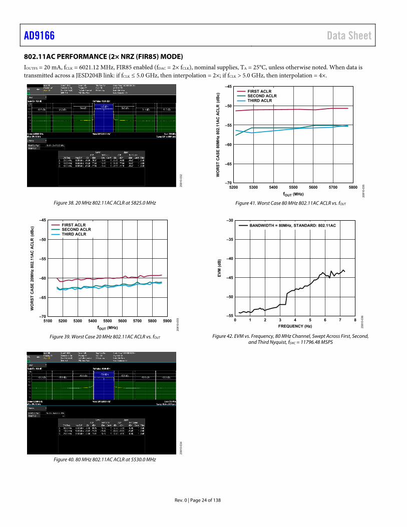
802.11AC PERFORMANCE (2× NRZ (FIR85) MODE) IOUTFS = 20 mA, fCLK = 6021.12 MHz, FIR85 enabled (fDAC = 2× fCLK), nominal supplies, TA = 25°C, unless otherwise noted. When data is transmitted across a JESD204B link: if fCLK ≤ 5.0 GHz, then interpolation = 2×; if fCLK > 5.0 GHz, then interpolation = 4×.
2081
0-03
2
Figure 38. 20 MHz 802.11AC ACLR at 5825.0 MHz
–45
–60
–50
–65
–70
–55
5100 59005600 5700 58005500540053005200
WO
RST
CASE
20M
Hz
802.
11A
C AC
LR (d
Bc)
fOUT (MHz)
SECOND ACLRFIRST ACLR
THIRD ACLR
2081
0-03
3
Figure 39. Worst Case 20 MHz 802.11AC ACLR vs. fOUT
2081
0-03
4
Figure 40. 80 MHz 802.11AC ACLR at 5530.0 MHz
–45
–60
–50
–65
–70
–55
5200 58005600 5700550054005300
WO
RST
CASE
80M
Hz
802.
11A
C AC
LR (d
Bc)
fOUT (MHz)
SECOND ACLRFIRST ACLR
THIRD ACLR
2081
0-03
5
Figure 41. Worst Case 80 MHz 802.11AC ACLR vs. fOUT
–30
–35
–40
–45
–50
–550 1 3 4 5 6 72 8
EVM
(dB)
FREQUENCY (Hz)
BANDWIDTH = 80MHz, STANDARD: 802.11AC
2081
0-03
6
Figure 42. EVM vs. Frequency, 80 MHz Channel, Swept Across First, Second, and Third Nyquist, fDAC = 11796.48 MSPS
Data Sheet AD9166
Rev. 0 | Page 25 of 138
TERMINOLOGY Offset Error Offset error is the deviation of the DAC output current from the ideal of 0 mA.
Gain Error Gain error is the difference between the actual and ideal output span. The actual span is determined by the difference between the output when the input is at its minimum code and the output when the input is at its maximum code.
Temperature Drift Temperature drift is specified as the maximum change from the ambient (25°C) value to the value at either TMIN or TMAX. For offset and gain drift, the drift is reported in ppm of full-scale range (FSR) per degree Celsius. For reference drift, the drift is reported in ppm per degree Celsius.
Settling Time Settling time is the time required for the output to reach and remain within a specified error band around its final value, measured from the start of the output transition.
Spurious-Free Dynamic Range (SFDR) SFDR is the difference, in decibels relative to carrier (dBc), between the peak amplitude of the output signal and the peak spurious signal within the dc to Nyquist frequency of the DAC. Typically, energy in this band is rejected by the interpolation filters. This specification, therefore, defines how well the interpolation filters work and the effect of other parasitic coupling paths on the DAC output.
x-Order Intermodulation Distortion (IMDx) IMDx (where x is 2, 3, 5, or 7 for second-order, third-order, fifth-order, or seventh-order intermodulation distortion) is the difference, in decibels relative to carrier (dBc), between the peak amplitude of the output signal and the peak intermodulation product of a specific x-order within the dc to Nyquist frequency of the DAC. The signal is composed of two continuous wave tones. If multiple IMDx products are present, the IMDx that is located nearest to the signal and containing the highest power is chosen to calculate the difference. This specification defines the linearity of the analog output stage.
Signal-to-Noise Ratio (SNR) SNR is the ratio of the rms value of the measured output signal to the rms sum of all other spectral components below the Nyquist frequency, excluding the first six harmonics and dc. The value for SNR is expressed in decibels.
Error Vector Magnitude (EVM) EVM defines the average deviation of a modulation symbol from its ideal location within a decision boundary. Typically, EVM is quoted as the rms average of all error vector magnitudes between the received symbols and their ideal locations, for a given modulation order. For example, EVM for a quadrature phase shift keying (QPSK) signal is the average of the EVM across four decision boundaries. EVM is measured using a baseband signal that is a pseudorandom binary sequence (PRBS) of a statistically significant length.
Interpolation Filter If the digital inputs to the DAC are sampled at a multiple rate of the interpolation rate (fDATA), a digital filter can be constructed that has a sharp transition band near fDATA/2. Images that typically appear around the output data rate (fDAC) can be greatly suppressed.
Adjacent Channel Leakage Ratio (ACLR) ACLR is the ratio in decibels relative to the carrier (dBc) between the measured power within a channel relative to its adjacent channel.
Adjusted DAC Update Rate The adjusted DAC update rate is the DAC update rate divided by the smallest interpolating factor. For clarity on DACs with multiple interpolating factors, the adjusted DAC update rate for each interpolating factor can be given.
Physical Lane Physical Lane x refers to SERDINx±, where x represents 0 to 7.
Logical Lane Logical Lane x (where x represents 0 to 7) refers to physical lanes after optionally being remapped by the crossbar block (Register 0x308 to Register 0x30B).
Link Lane Link Lane x refers to logical lanes considered in the link, where x represents 0 to 7.
AD9166 Data Sheet
Rev. 0 | Page 26 of 138
THEORY OF OPERATION The AD9166 is a high performance, wideband, transmit subsystem, composed of a high speed JESD204B SERDES interface, a flexible 16-bit digital datapath, a I/Q DAC core, along with an integrated differential to single-ended buffer amplifier that is matched to a 50 Ω load at dc to 10 GHz.
The AD9166 DAC core uses the patented quad-switch architecture, which enable DAC decoder settings that can extend the output frequency range into the second and third Nyquist zones with mix mode , RZ mode, and 2× NRZ mode (with FIR85 enabled). The output can cover a range from 0 Hz to more than 9 GHz in 2× NRZ mode. Mix mode can be used to access 1.5 GHz to around 9 GHz at a reduced device power consumption when compared to 2× NRZ. The NCO can then shift a signal of up to 1.8 GHz instantaneous bandwidth to the desired fOUT.
Figure 1 shows a functional block diagram of the AD9166. Eight high speed serial lanes carry data at a maximum speed of 12.5 Gbps, and either a 5 GSPS real input or a 2.5 GSPS complex input data rate to the digital datapath. Compared to either LVDS or CMOS interfaces, the SERDES interface simplifies pin count, board layout, and input clock requirements to the device.
The clock for the input data is derived from the device clock (required by the JESD204B specification). This device clock is sourced with a high fidelity, direct, external device sampling clock. The performance of the DAC core can be optimized by using on-chip adjustments to the device clock input accessible through the SPI port. The SERDES interface can be configured to operate in one-lane, two-lane, three-lane, four-lane, six-lane, or eight-lane mode, depending on the required input data rate.
The digital datapath of the AD9166 offers a bypass (1×) mode and several interpolation modes (2×, 3×, 4×, 6×, 8×, 12×, 16×, and 24×) through either an initial half-band (2×) or third-band (3×) filter with programmable 80% or 90% bandwidth, and three subsequent half-band filters (all 90%) with a maximum DAC core sample rate of 6.0 GSPS. An inverse sinc filter is provided to compensate for sinc related roll-off. An additional half-band filter, FIR85, takes advantage of the quad-switch architecture to interpolate on the falling edge of the clock, and effectively double the DAC update rate in 2× NRZ mode. A 48-bit programmable modulus numerically controlled oscillator (NCO) is provided to enable digital frequency shifts of signals with near infinite precision. The NCO can be operated alone in NCO only mode or with digital data from the SERDES interface and
digital datapath. The 100 MHz speed of the SPI write interface enables rapid updating of the frequency tuning word (FTW) of the NCO.
In addition to the main 48-bit NCO, the AD9166 also offers an FFH NCO for selected DDS applications. The FFH NCO consists of 32, 32-bit NCOs, each with its own phase accumulator, a FTW select register to select one of the NCOs, and a phase coherent hopping mode. Together, these elements enable phase coherent FFH. With the FTW select register and the 100 MHz SPI, dwell times as fast as 260 ns can be achieved.
The differential core output is buffered and converted to a single-ended output. The buffer is designed using a proprietary BiCMOS process, which greatly improves the spectral response of the core at higher operating frequencies. The improved spectral response is essential for applications where extra wide signal bandwidth and spectral flatness and purity are required. Its output has impedance match to 50 Ω, up to 10 GHz, which eases impedance matching concerns in wideband applications. The differential to single-ended buffer eliminates the need for an expensive, wideband balun, and supports the full operating range of the DAC core, from true dc to 9 GHz. DC coupling also allows baseband waveform generation, eliminating the need for external bias tees or similar circuitry.
The AD9166 is capable of multichip synchronization that can both synchronize multiple subsystems and establish a constant and deterministic latency (latency locking) path to the subsystem output. The latency for each of the subsystems remains constant to within several device clock cycles from link establishment to link establishment. An external alignment (SYSREF+ or SYSREF−) signal makes the AD9166 Subclass 1 compliant. Several modes of SYSREF± signal handling are available for use in the system.
An SPI configures the various functional blocks and monitors their statuses. The various functional blocks and the data interface must be set up in a specific sequence for proper operation (see the Start-Up Sequence section). Simple SPI initialization routines set up the JESD204B link and are included in the evaluation board package. This data sheet describes the various blocks of the AD9166 in greater detail. Descriptions of the JESD204B interface, control parameters, and various registers to set up and monitor the device are provided. The recommended start-up routine reliably sets up the data link.
Data Sheet AD9166
Rev. 0 | Page 27 of 138
SERIAL PORT OPERATION The AD9166 includes two separate SPI controllers, one for the DAC and one for the amplifier. Either the DAC or the amplifier can be addressed using the same SDIO, SDO, and SCLK pins, while asserting the corresponding chip select pin, CS_AMP or CS_DAC. CS_AMP and CS_DAC cannot be asserted simultaneously to address both the DAC and the amplifier during the same communication cycle, as described in the Chip Select (CS_AMP and CS_DAC) section.
The serial port is a flexible, synchronous serial communications port that allows easy interfacing with many industry-standard microcontrollers and microprocessors. The serial input/output (I/O) is compatible with most synchronous transfer formats, including both the Motorola SPI and Intel® SSR protocols. The interface allows read/write access to all registers that configure the AD9166. MSB first or LSB first transfer formats are supported. The serial port interface can be configured as a 4-wire interface or a 3-wire interface in which the input and output share a single-pin I/O (SDIO).
SCLK
SDO
SIO
CS_AMPSPI
PORTJ14
J13
J12
M13CS_DAC
B14
2081
0-07
8
Figure 43. Serial Port Interface Pins
There are two phases to a communication cycle with the AD9166. Phase 1 is the instruction cycle (the writing of an instruction byte into the device), coincident with the first 16 SCLK rising edges. The instruction word provides the serial port controller with information regarding the data transfer cycle, Phase 2 of the communication cycle. The Phase 1 instruction word defines whether the upcoming data transfer is a read or write, along with the starting register address for the following data transfer.
A logic high on the pin followed by a logic low resets the serial port timing to the initial state of the instruction cycle. From this state, the next 16 rising SCLK edges represent the instruction bits of the current I/O operation.
The remaining SCLK edges are for Phase 2 of the communication cycle. Phase 2 is the actual data transfer between the device and the system controller. Phase 2 of the communication cycle is a transfer of one or more data bytes. Eight × N SCLK cycles are needed to transfer N bytes during the transfer cycle. Registers change immediately upon writing to the last bit of each transfer byte, except for the FTW and NCO phase offsets, which change only when the frequency tuning word FTW_LOAD_REQ bit is set.
A logic high on CS_AMP or CS_DAC followed by a logic low resets the serial port timing to the initial state of the instruction cycle. From this state, the next 16 rising SCLK edges represent the instruction bits of the current I/O operation.
The remaining SCLK edges are for Phase 2 of the communication cycle. Phase 2 is the actual data transfer between the device and the system controller. Phase 2 of the communication cycle is a transfer of one or more data bytes. Eight × N SCLK cycles are needed to transfer N bytes during the transfer cycle. Registers change immediately upon writing to the last bit of each transfer byte, except for the FTW and NCO phase offsets, which change only when the frequency tuning word bit, FTW_LOAD_REQ, is set.
DATA FORMAT The instruction byte contains the information listed in Table 14.
Table 14. Serial Port Instruction Word I15 (MSB) I[14:0] R/W A[14:0]
R/W, Bit I15 of the instruction word, determines whether a read or a write data transfer occurs after the instruction word write. Logic 1 indicates a read operation, and Logic 0 indicates a write operation.
A14 to A0, Bit I14 to Bit I0 of the instruction word, determine the register that is accessed during the data transfer portion of the communication cycle. For multibyte transfers, A[14:0] is the starting address. The remaining register addresses are generated by the device based on the address increment bit. If the address increment bits are set high (Register 0x000, Bit 5 and Bit 2), multi-byte SPI writes start on A[14:0] and increment by 1 for every eight bits sent or received. If the address increment bits are set to 0, the address decrements by 1 every eight bits.
SERIAL PORT PIN DESCRIPTIONS Serial Clock (SCLK)
The serial clock pin synchronizes data to and from the device and runs the internal state machines. The maximum frequency of SCLK is 100 MHz. All data input is registered on the rising edge of SCLK. All data is driven out on the falling edge of SCLK.
Chip Select (CS_AMP and CS_DAC)
The AD9166 includes two chip select pins, one for the DAC (CS_DAC) and one for the buffer amplifier (CS_AMP), hereafter referred to as CS_x. The correct CS_x pin must be asserted to address the particular silicon die. CS_AMP and CS_DAC cannot be asserted simultaneously.
An active low input starts and gates a communication cycle. CS_x allows more than one device to be used on the same serial communications line. The SDIO pin goes to a high impedance state when this input is high. During the communication cycle, the chip select must stay low.
Serial Data I/O (SDIO)
The SDIO pin is a bidirectional data line. In 4-wire mode, the SDIO pin acts as the data input and the SDO pin acts as the data output.
AD9166 Data Sheet
Rev. 0 | Page 28 of 138
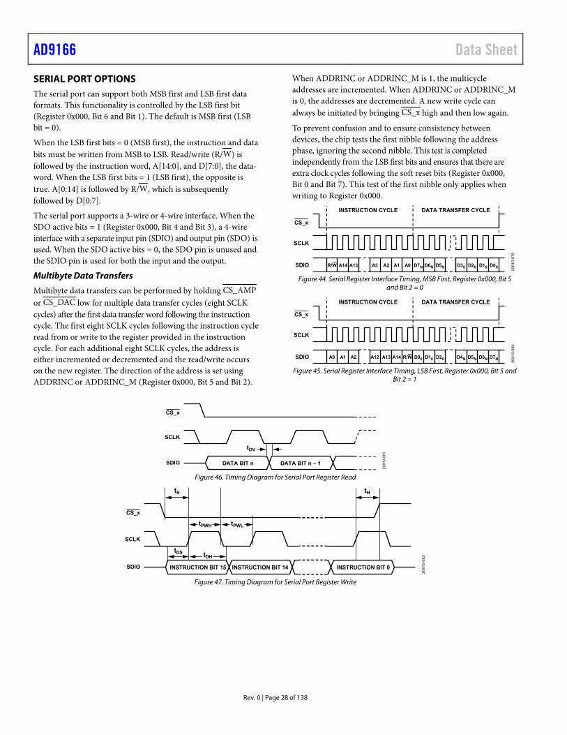
SERIAL PORT OPTIONS The serial port can support both MSB first and LSB first data formats. This functionality is controlled by the LSB first bit (Register 0x000, Bit 6 and Bit 1). The default is MSB first (LSB bit = 0).
When the LSB first bits = 0 (MSB first), the instruction and data bits must be written from MSB to LSB. Read/write (R/W) is followed by the instruction word, A[14:0], and D[7:0], the data-word. When the LSB first bits = 1 (LSB first), the opposite is true. A[0:14] is followed by R/W, which is subsequently followed by D[0:7].
The serial port supports a 3-wire or 4-wire interface. When the SDO active bits = 1 (Register 0x000, Bit 4 and Bit 3), a 4-wire interface with a separate input pin (SDIO) and output pin (SDO) is used. When the SDO active bits = 0, the SDO pin is unused and the SDIO pin is used for both the input and the output.
Multibyte Data Transfers
Multibyte data transfers can be performed by holding CS_AMP or CS_DAC low for multiple data transfer cycles (eight SCLK cycles) after the first data transfer word following the instruction cycle. The first eight SCLK cycles following the instruction cycle read from or write to the register provided in the instruction cycle. For each additional eight SCLK cycles, the address is either incremented or decremented and the read/write occurs on the new register. The direction of the address is set using ADDRINC or ADDRINC_M (Register 0x000, Bit 5 and Bit 2).
When ADDRINC or ADDRINC_M is 1, the multicycle addresses are incremented. When ADDRINC or ADDRINC_M is 0, the addresses are decremented. A new write cycle can always be initiated by bringing CS_x high and then low again.
To prevent confusion and to ensure consistency between devices, the chip tests the first nibble following the address phase, ignoring the second nibble. This test is completed independently from the LSB first bits and ensures that there are extra clock cycles following the soft reset bits (Register 0x000, Bit 0 and Bit 7). This test of the first nibble only applies when writing to Register 0x000.
R/W A14 A13 A3 A2 A1 A0 D7N D6N D5N D00D10D20D30
INSTRUCTION CYCLE DATA TRANSFER CYCLE
SCLK
SDIO
CS_x
2081
0-07
9
Figure 44. Serial Register Interface Timing, MSB First, Register 0x000, Bit 5
and Bit 2 = 0
A0 A1 A2 A12 A13 A14 D00 D10 D20 D7ND6ND5ND4N
INSTRUCTION CYCLE DATA TRANSFER CYCLE
SCLK
SDIO R/W
2081
0-08
0
CS_x
Figure 45. Serial Register Interface Timing, LSB First, Register 0x000, Bit 5 and
Bit 2 = 1
SCLK
SDIO
CS_x
DATA BIT n – 1DATA BIT n
tDV
2081
0-08
1
Figure 46. Timing Diagram for Serial Port Register Read
SCLK
SDIO
CS_x
INSTRUCTION BIT 14 INSTRUCTION BIT 0INSTRUCTION BIT 15
tS
tDS tDH
tPWH tPWL
tH
2081
0-08
2
Figure 47. Timing Diagram for Serial Port Register Write
Data Sheet AD9166
Rev. 0 | Page 29 of 138
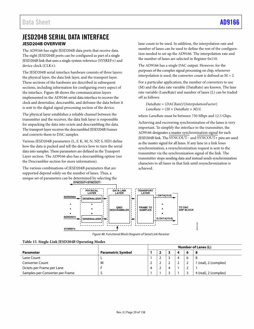
JESD204B SERIAL DATA INTERFACE JESD204B OVERVIEW The AD9166 has eight JESD204B data ports that receive data. The eight JESD204B ports can be configured as part of a single JESD204B link that uses a single system reference (SYSREF±) and device clock (CLK±).
The JESD204B serial interface hardware consists of three layers: the physical layer, the data link layer, and the transport layer. These sections of the hardware are described in subsequent sections, including information for configuring every aspect of the interface. Figure 48 shows the communication layers implemented in the AD9166 serial data interface to recover the clock and deserialize, descramble, and deframe the data before it is sent to the digital signal processing section of the device.
The physical layer establishes a reliable channel between the transmitter and the receiver, the data link layer is responsible for unpacking the data into octets and descrambling the data. The transport layer receives the descrambled JESD204B frames and converts them to DAC samples.
Various JESD204B parameters (L, F, K, M, N, NP, S, HD) define how the data is packed and tell the device how to turn the serial data into samples. These parameters are defined in the Transport Layer section. The AD9166 also has a descrambling option (see the Descrambler section for more information).
The various combinations of JESD204B parameters that are supported depend solely on the number of lanes. Thus, a unique set of parameters can be determined by selecting the
lane count to be used. In addition, the interpolation rate and number of lanes can be used to define the rest of the configura-tion needed to set up the AD9166. The interpolation rate and the number of lanes are selected in Register 0x110.
The AD9166 has a single DAC output. However, for the purposes of the complex signal processing on chip, whenever interpolation is used, the converter count is defined as M = 2.
For a particular application, the number of converters to use (M) and the data rate variable (DataRate) are known. The lane rate variable (LaneRate) and number of lanes (L) can be traded off as follows:
DataRate = (DACRate)/(InterpolationFactor) LaneRate = (20 × DataRate × M)/L
where LaneRate must be between 750 Mbps and 12.5 Gbps.
Achieving and recovering synchronization of the lanes is very important. To simplify the interface to the transmitter, the AD9166 designates a master synchronization signal for each JESD204B link. The SYNCOUT− and SYNCOUT+ pins are used as the master signal for all lanes. If any lane in a link loses synchronization, a resynchronization request is sent to the transmitter via the synchronization signal of the link. The transmitter stops sending data and instead sends synchronization characters to all lanes in that link until resynchronization is achieved.
DESERIALIZER
DATA LINKLAYER
TRANSPORTLAYER
SERDIN0±
SYSREF±
SERDIN7±
I DATA[15:0]
Q DATA[15:0]
TO DACDSP BLOCK
SYNCOUT+/SYNCOUT–
PHYSICALLAYER
DESERIALIZER
QBD/DESCRAMBLER
FRAME TOSAMPLES
2081
0-08
3
Figure 48. Functional Block Diagram of Serial Link Receiver
Table 15. Single-Link JESD204B Operating Modes Number of Lanes (L) Parameter Parametric Symbol 1 2 3 4 6 8 Lane Count L 1 2 3 4 6 8 Converter Count M 2 2 2 2 2 1 (real), 2 (complex) Octets per Frame per Lane F 4 2 4 1 2 1 Samples per Converter per Frame S 1 1 3 1 3 4 (real), 2 (complex)
AD9166 Data Sheet
Rev. 0 | Page 30 of 138
Table 16. Data Structure per Lane for JESD204B Operating Modes1 JESD204B Operating Mode Lane No. Frame 0 Frame 1 Frame 2 Frame 3 L = 8, M = 1, F = 1, S = 4 Lane 0 M0S0[15:8] Lane 1 M0S0[7:0] Lane 2 M0S1[15:8] Lane 3 M0S1[7:0] Lane 4 M0S2[15:8] Lane 5 M0S2[7:0] Lane 6 M0S3[15:8] Lane 7 M0S3[7:0] L = 8, M = 2, F = 1, S = 2 Lane 0 M0S0[15:8] Lane 1 M0S0[7:0] Lane 2 M0S1[15:8] Lane 3 M0S1[7:0] Lane 4 M1S0[15:8] Lane 5 M1S0[7:0] Lane 6 M1S1[15:8] Lane 7 M1S1[7:0] L = 6, M = 2, F = 2, S = 3 Lane 0 M0S0[15:8] M0S0[7:0] Lane 1 M0S1[15:8] M0S1[7:0] Lane 2 M0S2[15:8] M0S2[7:0] Lane 3 M1S0[15:8] M1S0[7:0] Lane 4 M1S1[15:8] M1S1[7:0] Lane 5 M1S2[15:8] M1S2[7:0] L = 4, M = 2, F = 1, S = 1 Lane 0 M0S0[15:8] Lane 1 M0S0[7:0] Lane 2 M1S0[15:8] Lane 3 M1S0[7:0] L = 3, M = 2, F = 4, S = 3 Lane 0 M0S0[15:8] M0S0[7:0] M0S1[15:8] M0S1[7:0] Lane 1 M0S2[15:8] M0S2[7:0] M1S0[15:8] M1S0[7:0] Lane 2 M1S1[15:8] M1S1[7:0] M1S2[15:8] M1S2[7:0] L = 2, M = 2, F = 2, S = 1 Lane 0 M0S0[15:8] M0S0[7:0] Lane 1 M1S0[15:8] M1S0[7:0] L = 1, M = 2, F = 4, S = 1 Lane 0 M0S0[15:8] M0S0[7:0] M1S0[15:8] M1S0[7:0] 1 Mx is the converter number and Sy is the sample number. For example, M0S0 means Converter 0, Sample 0. Blank cells are not applicable.
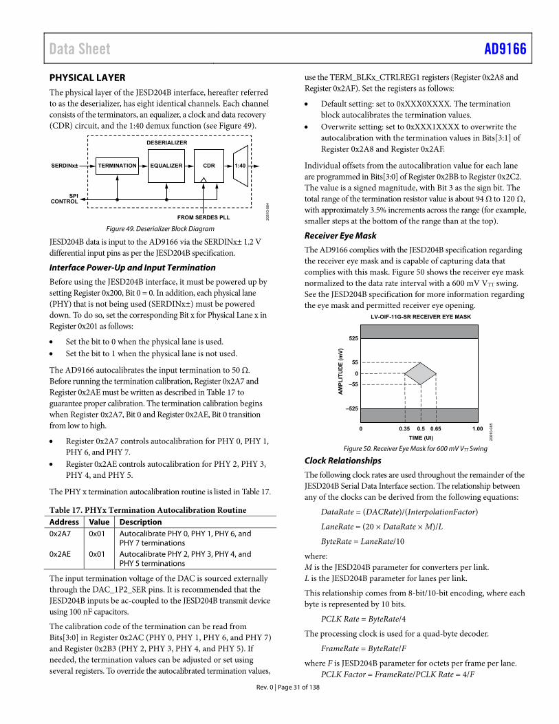
Data Sheet AD9166
Rev. 0 | Page 31 of 138
PHYSICAL LAYER The physical layer of the JESD204B interface, hereafter referred to as the deserializer, has eight identical channels. Each channel consists of the terminators, an equalizer, a clock and data recovery (CDR) circuit, and the 1:40 demux function (see Figure 49).
EQUALIZER CDR 1:40
DESERIALIZER
FROM SERDES PLL
SPICONTROL
TERMINATIONSERDINx±
2081
0-08
4
Figure 49. Deserializer Block Diagram
JESD204B data is input to the AD9166 via the SERDINx± 1.2 V differential input pins as per the JESD204B specification.
Interface Power-Up and Input Termination
Before using the JESD204B interface, it must be powered up by setting Register 0x200, Bit 0 = 0. In addition, each physical lane (PHY) that is not being used (SERDINx±) must be powered down. To do so, set the corresponding Bit x for Physical Lane x in Register 0x201 as follows:
Set the bit to 0 when the physical lane is used. Set the bit to 1 when the physical lane is not used.
The AD9166 autocalibrates the input termination to 50 Ω. Before running the termination calibration, Register 0x2A7 and Register 0x2AE must be written as described in Table 17 to guarantee proper calibration. The termination calibration begins when Register 0x2A7, Bit 0 and Register 0x2AE, Bit 0 transition from low to high.
Register 0x2A7 controls autocalibration for PHY 0, PHY 1, PHY 6, and PHY 7.
Register 0x2AE controls autocalibration for PHY 2, PHY 3, PHY 4, and PHY 5.
The PHY x termination autocalibration routine is listed in Table 17.
Table 17. PHYx Termination Autocalibration Routine Address Value Description 0x2A7 0x01 Autocalibrate PHY 0, PHY 1, PHY 6, and
PHY 7 terminations 0x2AE 0x01 Autocalibrate PHY 2, PHY 3, PHY 4, and
PHY 5 terminations
The input termination voltage of the DAC is sourced externally through the DAC_1P2_SER pins. It is recommended that the JESD204B inputs be ac-coupled to the JESD204B transmit device using 100 nF capacitors.
The calibration code of the termination can be read from Bits[3:0] in Register 0x2AC (PHY 0, PHY 1, PHY 6, and PHY 7) and Register 0x2B3 (PHY 2, PHY 3, PHY 4, and PHY 5). If needed, the termination values can be adjusted or set using several registers. To override the autocalibrated termination values,
use the TERM_BLKx_CTRLREG1 registers (Register 0x2A8 and Register 0x2AF). Set the registers as follows:
Default setting: set to 0xXXX0XXXX. The termination block autocalibrates the termination values.
Overwrite setting: set to 0xXXX1XXXX to overwrite the autocalibration with the termination values in Bits[3:1] of Register 0x2A8 and Register 0x2AF.
Individual offsets from the autocalibration value for each lane are programmed in Bits[3:0] of Register 0x2BB to Register 0x2C2. The value is a signed magnitude, with Bit 3 as the sign bit. The total range of the termination resistor value is about 94 Ω to 120 Ω, with approximately 3.5% increments across the range (for example, smaller steps at the bottom of the range than at the top).
Receiver Eye Mask
The AD9166 complies with the JESD204B specification regarding the receiver eye mask and is capable of capturing data that complies with this mask. Figure 50 shows the receiver eye mask normalized to the data rate interval with a 600 mV VTT swing. See the JESD204B specification for more information regarding the eye mask and permitted receiver eye opening.
525
55
0
–55
–525
AMPL
ITUD
E (m
V)
0 0.5 1.000.35 0.65TIME (UI)
LV-OIF-11G-SR RECEIVER EYE MASK
2081
0-08
5
Figure 50. Receiver Eye Mask for 600 mV VTT Swing
Clock Relationships
The following clock rates are used throughout the remainder of the JESD204B Serial Data Interface section. The relationship between any of the clocks can be derived from the following equations:
DataRate = (DACRate)/(InterpolationFactor)
LaneRate = (20 × DataRate × M)/L
ByteRate = LaneRate/10
where: M is the JESD204B parameter for converters per link. L is the JESD204B parameter for lanes per link.
This relationship comes from 8-bit/10-bit encoding, where each byte is represented by 10 bits.
PCLK Rate = ByteRate/4
The processing clock is used for a quad-byte decoder.
FrameRate = ByteRate/F
where F is JESD204B parameter for octets per frame per lane. PCLK Factor = FrameRate/PCLK Rate = 4/F
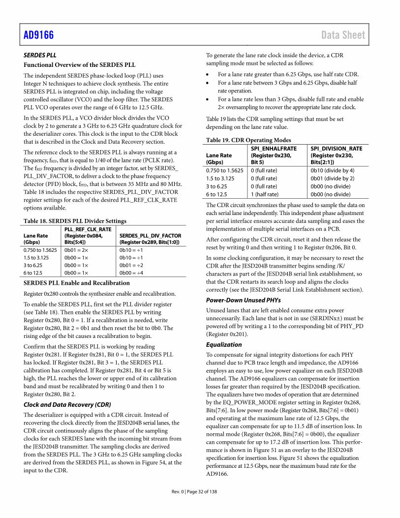
AD9166 Data Sheet
Rev. 0 | Page 32 of 138
SERDES PLL
Functional Overview of the SERDES PLL
The independent SERDES phase-locked loop (PLL) uses Integer N techniques to achieve clock synthesis. The entire SERDES PLL is integrated on chip, including the voltage controlled oscillator (VCO) and the loop filter. The SERDES PLL VCO operates over the range of 6 GHz to 12.5 GHz.
In the SERDES PLL, a VCO divider block divides the VCO clock by 2 to generate a 3 GHz to 6.25 GHz quadrature clock for the deserializer cores. This clock is the input to the CDR block that is described in the Clock and Data Recovery section.
The reference clock to the SERDES PLL is always running at a frequency, fREF, that is equal to 1/40 of the lane rate (PCLK rate). The fREF frequency is divided by an integer factor, set by SERDES_ PLL_DIV_FACTOR, to deliver a clock to the phase frequency detector (PFD) block, fPFD, that is between 35 MHz and 80 MHz. Table 18 includes the respective SERDES_PLL_DIV_FACTOR register settings for each of the desired PLL_REF_CLK_RATE options available.
Table 18. SERDES PLL Divider Settings
Lane Rate (Gbps)
PLL_REF_CLK_RATE (Register 0x084, Bits[5:4])
SERDES_PLL_DIV_FACTOR (Register 0x289, Bits[1:0])
0.750 to 1.5625 0b01 = 2× 0b10 = ÷1 1.5 to 3.125 0b00 = 1× 0b10 = ÷1 3 to 6.25 0b00 = 1× 0b01 = ÷2 6 to 12.5 0b00 = 1× 0b00 = ÷4
SERDES PLL Enable and Recalibration
Register 0x280 controls the synthesizer enable and recalibration.
To enable the SERDES PLL, first set the PLL divider register (see Table 18). Then enable the SERDES PLL by writing Register 0x280, Bit 0 = 1. If a recalibration is needed, write Register 0x280, Bit 2 = 0b1 and then reset the bit to 0b0. The rising edge of the bit causes a recalibration to begin.
Confirm that the SERDES PLL is working by reading Register 0x281. If Register 0x281, Bit 0 = 1, the SERDES PLL has locked. If Register 0x281, Bit 3 = 1, the SERDES PLL calibration has completed. If Register 0x281, Bit 4 or Bit 5 is high, the PLL reaches the lower or upper end of its calibration band and must be recalibrated by writing 0 and then 1 to Register 0x280, Bit 2.
Clock and Data Recovery (CDR)
The deserializer is equipped with a CDR circuit. Instead of recovering the clock directly from the JESD204B serial lanes, the CDR circuit continuously aligns the phase of the sampling clocks for each SERDES lane with the incoming bit stream from the JESD204B transmitter. The sampling clocks are derived from the SERDES PLL. The 3 GHz to 6.25 GHz sampling clocks are derived from the SERDES PLL, as shown in Figure 54, at the input to the CDR.
To generate the lane rate clock inside the device, a CDR sampling mode must be selected as follows:
For a lane rate greater than 6.25 Gbps, use half rate CDR. For a lane rate between 3 Gbps and 6.25 Gbps, disable half
rate operation. For a lane rate less than 3 Gbps, disable full rate and enable
2× oversampling to recover the appropriate lane rate clock.
Table 19 lists the CDR sampling settings that must be set depending on the lane rate value.
Table 19. CDR Operating Modes
Lane Rate (Gbps)
SPI_ENHALFRATE (Register 0x230, Bit 5)
SPI_DIVISION_RATE (Register 0x230, Bits[2:1])
0.750 to 1.5625 0 (full rate) 0b10 (divide by 4) 1.5 to 3.125 0 (full rate) 0b01 (divide by 2) 3 to 6.25 0 (full rate) 0b00 (no divide) 6 to 12.5 1 (half rate) 0b00 (no divide)
The CDR circuit synchronizes the phase used to sample the data on each serial lane independently. This independent phase adjustment per serial interface ensures accurate data sampling and eases the implementation of multiple serial interfaces on a PCB.
After configuring the CDR circuit, reset it and then release the reset by writing 0 and then writing 1 to Register 0x206, Bit 0.
In some clocking configuration, it may be necessary to reset the CDR after the JESD204B transmitter begins sending /K/ characters as part of the JESD204B serial link establishment, so that the CDR restarts its search loop and aligns the clocks correctly (see the JESD204B Serial Link Establishment section).
Power-Down Unused PHYs
Unused lanes that are left enabled consume extra power unnecessarily. Each lane that is not in use (SERDINx±) must be powered off by writing a 1 to the corresponding bit of PHY_PD (Register 0x201).
Equalization
To compensate for signal integrity distortions for each PHY channel due to PCB trace length and impedance, the AD9166 employs an easy to use, low power equalizer on each JESD204B channel. The AD9166 equalizers can compensate for insertion losses far greater than required by the JESD204B specification. The equalizers have two modes of operation that are determined by the EQ_POWER_MODE register setting in Register 0x268, Bits[7:6]. In low power mode (Register 0x268, Bits[7:6] = 0b01) and operating at the maximum lane rate of 12.5 Gbps, the equalizer can compensate for up to 11.5 dB of insertion loss. In normal mode (Register 0x268, Bits[7:6] = 0b00), the equalizer can compensate for up to 17.2 dB of insertion loss. This perfor-mance is shown in Figure 51 as an overlay to the JESD204B specification for insertion loss. Figure 51 shows the equalization performance at 12.5 Gbps, near the maximum baud rate for the AD9166.
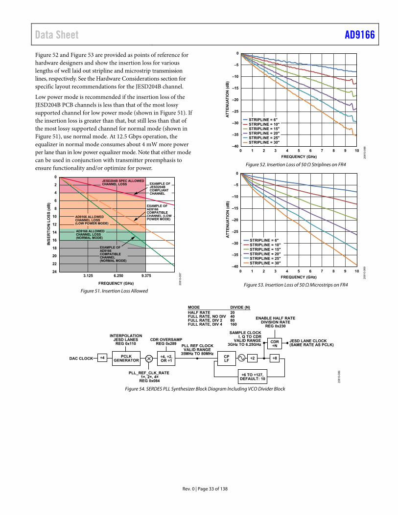
Data Sheet AD9166
Rev. 0 | Page 33 of 138
Figure 52 and Figure 53 are provided as points of reference for hardware designers and show the insertion loss for various lengths of well laid out stripline and microstrip transmission lines, respectively. See the Hardware Considerations section for specific layout recommendations for the JESD204B channel.
Low power mode is recommended if the insertion loss of the JESD204B PCB channels is less than that of the most lossy supported channel for low power mode (shown in Figure 51). If the insertion loss is greater than that, but still less than that of the most lossy supported channel for normal mode (shown in Figure 51), use normal mode. At 12.5 Gbps operation, the equalizer in normal mode consumes about 4 mW more power per lane than in low power equalizer mode. Note that either mode can be used in conjunction with transmitter preemphasis to ensure functionality and/or optimize for power.
FREQUENCY (GHz)
0
2
4
6
8
10
12
14
16
18
20
22
246.250 9.3753.125
AD9166 ALLOWEDCHANNEL LOSS(NORMAL MODE)
AD9166 ALLOWEDCHANNEL LOSS(LOW POWER MODE)
JESD204B SPEC ALLOWEDCHANNEL LOSS EXAMPLE OF
JESD204BCOMPLIANTCHANNEL
EXAMPLE OFAD9166COMPATIBLECHANNEL (LOWPOWER MODE)
EXAMPLE OFAD9166COMPATIBLECHANNEL(NORMAL MODE)
2081
0-08
7
Figure 51. Insertion Loss Allowed
–40
–35
–30
–25
–20
–15
–10
–5
0
0 1 2 3 4 5 6 7 8 9 10
ATTE
NUAT
ION
(dB)
FREQUENCY (GHz)
STRIPLINE = 6"STRIPLINE = 10"STRIPLINE = 15"STRIPLINE = 20"STRIPLINE = 25"STRIPLINE = 30"
2081
0-08
8
Figure 52. Insertion Loss of 50 Ω Striplines on FR4
–40
–35
–30
–25
–20
–15
–10
–5
0
ATTE
NUAT
ION
(dB)
FREQUENCY (GHz) 2081
0-08
9
STRIPLINE = 6"STRIPLINE = 10"STRIPLINE = 15"STRIPLINE = 20"STRIPLINE = 25"STRIPLINE = 30"
Figure 53. Insertion Loss of 50 Ω Microstrips on FR4
÷2 ÷8PCLKGENERATOR
÷4, ÷2,OR ÷1
CDR OVERSAMPREG 0x289 PLL REF CLOCK
VALID RANGE35MHz TO 80MHz
SAMPLE CLOCKI, Q TO CDR
VALID RANGE3GHz TO 6.25GHz
ENABLE HALF RATEDIVISION RATE
REG 0x230
JESD LANE CLOCK(SAME RATE AS PCLK)
INTERPOLATIONJESD LANESREG 0x110
PLL_REF_CLK_RATE1×, 2×, 4×
REG 0x084
DAC CLOCK
÷6 TO ÷127,DEFAULT: 10
CPLF
CDR÷N
÷4
MODEHALF RATEFULL RATE, NO DIVFULL RATE, DIV 2FULL RATE, DIV 4
DIVIDE (N)204080160
2081
0-08
6
Figure 54. SERDES PLL Synthesizer Block Diagram Including VCO Divider Block
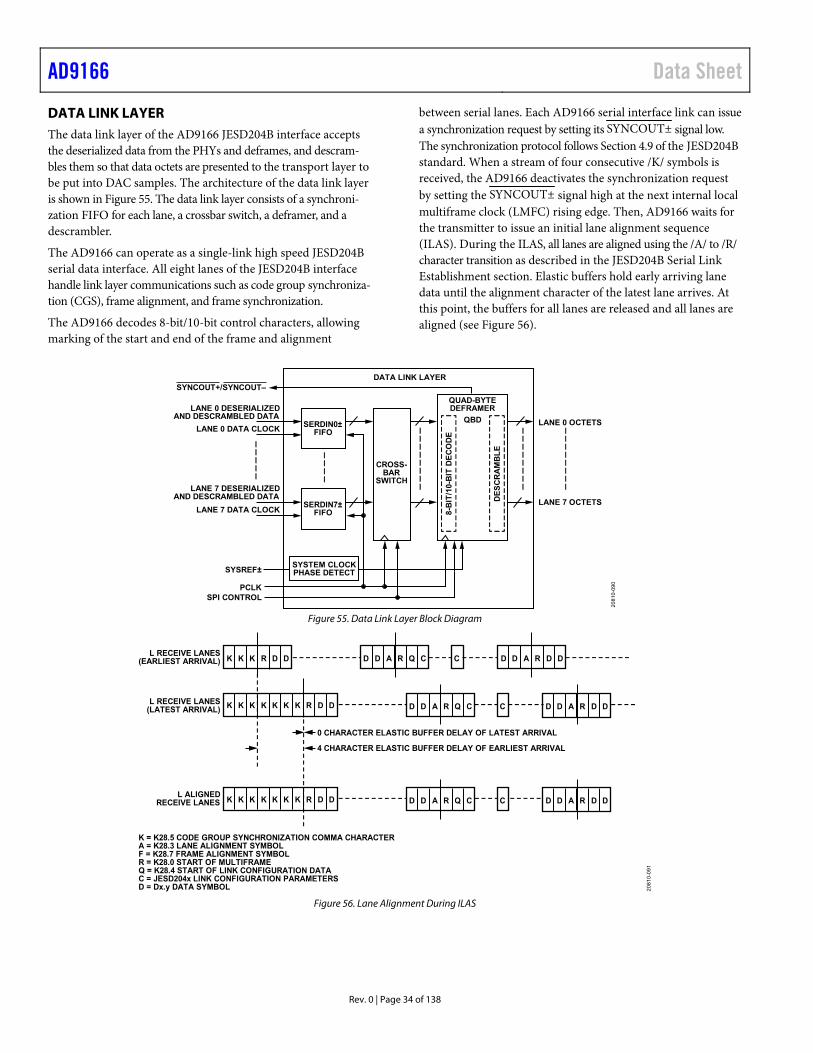
AD9166 Data Sheet
Rev. 0 | Page 34 of 138
DATA LINK LAYER The data link layer of the AD9166 JESD204B interface accepts the deserialized data from the PHYs and deframes, and descram-bles them so that data octets are presented to the transport layer to be put into DAC samples. The architecture of the data link layer is shown in Figure 55. The data link layer consists of a synchroni-zation FIFO for each lane, a crossbar switch, a deframer, and a descrambler.
The AD9166 can operate as a single-link high speed JESD204B serial data interface. All eight lanes of the JESD204B interface handle link layer communications such as code group synchroniza-tion (CGS), frame alignment, and frame synchronization.
The AD9166 decodes 8-bit/10-bit control characters, allowing marking of the start and end of the frame and alignment
between serial lanes. Each AD9166 serial interface link can issue a synchronization request by setting its SYNCOUT± signal low. The synchronization protocol follows Section 4.9 of the JESD204B standard. When a stream of four consecutive /K/ symbols is received, the AD9166 deactivates the synchronization request by setting the SYNCOUT± signal high at the next internal local multiframe clock (LMFC) rising edge. Then, AD9166 waits for the transmitter to issue an initial lane alignment sequence (ILAS). During the ILAS, all lanes are aligned using the /A/ to /R/ character transition as described in the JESD204B Serial Link Establishment section. Elastic buffers hold early arriving lane data until the alignment character of the latest lane arrives. At this point, the buffers for all lanes are released and all lanes are aligned (see Figure 56).
LANE 0 DESERIALIZEDAND DESCRAMBLED DATA
LANE 0 DATA CLOCK SERDIN0±FIFO
SERDIN7±FIFO
CROSS-BAR
SWITCHLANE 7 DESERIALIZED
AND DESCRAMBLED DATALANE 7 DATA CLOCK
PCLK
DATA LINK LAYER
SPI CONTROL
SYSREF±
DESC
RAM
BLE
8-BI
T/10
-BIT
DEC
ODE
SYSTEM CLOCKPHASE DETECT
LANE 0 OCTETS
LANE 7 OCTETS
QUAD-BYTEDEFRAMER
QBD
2081
0-09
0
SYNCOUT+/SYNCOUT–
Figure 55. Data Link Layer Block Diagram
L RECEIVE LANES(LATEST ARRIVAL)
L ALIGNEDRECEIVE LANES
0 CHARACTER ELASTIC BUFFER DELAY OF LATEST ARRIVAL
K = K28.5 CODE GROUP SYNCHRONIZATION COMMA CHARACTERA = K28.3 LANE ALIGNMENT SYMBOLF = K28.7 FRAME ALIGNMENT SYMBOLR = K28.0 START OF MULTIFRAMEQ = K28.4 START OF LINK CONFIGURATION DATAC = JESD204x LINK CONFIGURATION PARAMETERSD = Dx.y DATA SYMBOL
4 CHARACTER ELASTIC BUFFER DELAY OF EARLIEST ARRIVAL
L RECEIVE LANES(EARLIEST ARRIVAL)
K K K K K K K R D D
K K K R D D D D A R Q C C
D D A R Q C C
D D A R D D
D D A R D D
K K K K K K K R D D D D A R Q C C D D A R D D
2081
0-09
1
Figure 56. Lane Alignment During ILAS
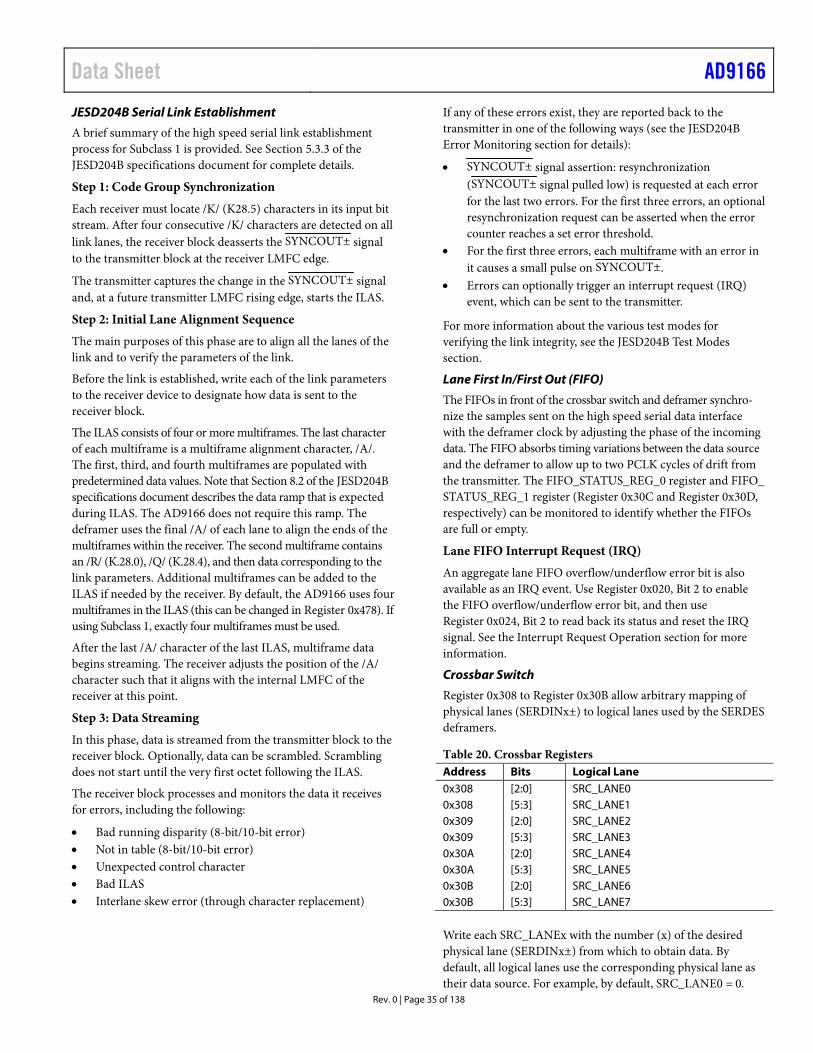
Data Sheet AD9166
Rev. 0 | Page 35 of 138
JESD204B Serial Link Establishment
A brief summary of the high speed serial link establishment process for Subclass 1 is provided. See Section 5.3.3 of the JESD204B specifications document for complete details.
Step 1: Code Group Synchronization
Each receiver must locate /K/ (K28.5) characters in its input bit stream. After four consecutive /K/ characters are detected on all link lanes, the receiver block deasserts the SYNCOUT± signal to the transmitter block at the receiver LMFC edge.
The transmitter captures the change in the SYNCOUT± signal and, at a future transmitter LMFC rising edge, starts the ILAS.
Step 2: Initial Lane Alignment Sequence
The main purposes of this phase are to align all the lanes of the link and to verify the parameters of the link.
Before the link is established, write each of the link parameters to the receiver device to designate how data is sent to the receiver block.
The ILAS consists of four or more multiframes. The last character of each multiframe is a multiframe alignment character, /A/. The first, third, and fourth multiframes are populated with predetermined data values. Note that Section 8.2 of the JESD204B specifications document describes the data ramp that is expected during ILAS. The AD9166 does not require this ramp. The deframer uses the final /A/ of each lane to align the ends of the multiframes within the receiver. The second multiframe contains an /R/ (K.28.0), /Q/ (K.28.4), and then data corresponding to the link parameters. Additional multiframes can be added to the ILAS if needed by the receiver. By default, the AD9166 uses four multiframes in the ILAS (this can be changed in Register 0x478). If using Subclass 1, exactly four multiframes must be used.
After the last /A/ character of the last ILAS, multiframe data begins streaming. The receiver adjusts the position of the /A/ character such that it aligns with the internal LMFC of the receiver at this point.
Step 3: Data Streaming
In this phase, data is streamed from the transmitter block to the receiver block. Optionally, data can be scrambled. Scrambling does not start until the very first octet following the ILAS.
The receiver block processes and monitors the data it receives for errors, including the following:
Bad running disparity (8-bit/10-bit error) Not in table (8-bit/10-bit error) Unexpected control character Bad ILAS Interlane skew error (through character replacement)
If any of these errors exist, they are reported back to the transmitter in one of the following ways (see the JESD204B Error Monitoring section for details):
SYNCOUT± signal assertion: resynchronization (SYNCOUT± signal pulled low) is requested at each error for the last two errors. For the first three errors, an optional resynchronization request can be asserted when the error counter reaches a set error threshold.
For the first three errors, each multiframe with an error in it causes a small pulse on SYNCOUT±.
Errors can optionally trigger an interrupt request (IRQ) event, which can be sent to the transmitter.
For more information about the various test modes for verifying the link integrity, see the JESD204B Test Modes section.
Lane First In/First Out (FIFO)
The FIFOs in front of the crossbar switch and deframer synchro-nize the samples sent on the high speed serial data interface with the deframer clock by adjusting the phase of the incoming data. The FIFO absorbs timing variations between the data source and the deframer to allow up to two PCLK cycles of drift from the transmitter. The FIFO_STATUS_REG_0 register and FIFO_ STATUS_REG_1 register (Register 0x30C and Register 0x30D, respectively) can be monitored to identify whether the FIFOs are full or empty.
Lane FIFO Interrupt Request (IRQ)
An aggregate lane FIFO overflow/underflow error bit is also available as an IRQ event. Use Register 0x020, Bit 2 to enable the FIFO overflow/underflow error bit, and then use Register 0x024, Bit 2 to read back its status and reset the IRQ signal. See the Interrupt Request Operation section for more information.
Crossbar Switch
Register 0x308 to Register 0x30B allow arbitrary mapping of physical lanes (SERDINx±) to logical lanes used by the SERDES deframers.
Table 20. Crossbar Registers Address Bits Logical Lane 0x308 [2:0] SRC_LANE0 0x308 [5:3] SRC_LANE1 0x309 [2:0] SRC_LANE2 0x309 [5:3] SRC_LANE3 0x30A [2:0] SRC_LANE4 0x30A [5:3] SRC_LANE5 0x30B [2:0] SRC_LANE6 0x30B [5:3] SRC_LANE7
Write each SRC_LANEx with the number (x) of the desired physical lane (SERDINx±) from which to obtain data. By default, all logical lanes use the corresponding physical lane as their data source. For example, by default, SRC_LANE0 = 0.
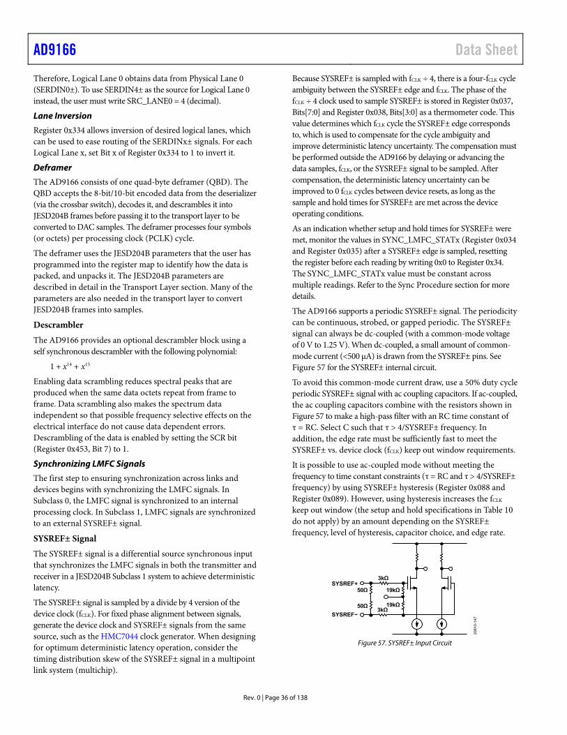
AD9166 Data Sheet
Rev. 0 | Page 36 of 138
Therefore, Logical Lane 0 obtains data from Physical Lane 0 (SERDIN0±). To use SERDIN4± as the source for Logical Lane 0 instead, the user must write SRC_LANE0 = 4 (decimal).
Lane Inversion
Register 0x334 allows inversion of desired logical lanes, which can be used to ease routing of the SERDINx± signals. For each Logical Lane x, set Bit x of Register 0x334 to 1 to invert it.
Deframer
The AD9166 consists of one quad-byte deframer (QBD). The QBD accepts the 8-bit/10-bit encoded data from the deserializer (via the crossbar switch), decodes it, and descrambles it into JESD204B frames before passing it to the transport layer to be converted to DAC samples. The deframer processes four symbols (or octets) per processing clock (PCLK) cycle.
The deframer uses the JESD204B parameters that the user has programmed into the register map to identify how the data is packed, and unpacks it. The JESD204B parameters are described in detail in the Transport Layer section. Many of the parameters are also needed in the transport layer to convert JESD204B frames into samples.
Descrambler
The AD9166 provides an optional descrambler block using a self synchronous descrambler with the following polynomial:
1 + x14 + x15
Enabling data scrambling reduces spectral peaks that are produced when the same data octets repeat from frame to frame. Data scrambling also makes the spectrum data independent so that possible frequency selective effects on the electrical interface do not cause data dependent errors. Descrambling of the data is enabled by setting the SCR bit (Register 0x453, Bit 7) to 1.
Synchronizing LMFC Signals
The first step to ensuring synchronization across links and devices begins with synchronizing the LMFC signals. In Subclass 0, the LMFC signal is synchronized to an internal processing clock. In Subclass 1, LMFC signals are synchronized to an external SYSREF± signal.
SYSREF± Signal
The SYSREF± signal is a differential source synchronous input that synchronizes the LMFC signals in both the transmitter and receiver in a JESD204B Subclass 1 system to achieve deterministic latency.
The SYSREF± signal is sampled by a divide by 4 version of the device clock (fCLK). For fixed phase alignment between signals, generate the device clock and SYSREF± signals from the same source, such as the HMC7044 clock generator. When designing for optimum deterministic latency operation, consider the timing distribution skew of the SYSREF± signal in a multipoint link system (multichip).
Because SYSREF± is sampled with fCLK ÷ 4, there is a four-fCLK cycle ambiguity between the SYSREF± edge and fCLK. The phase of the fCLK ÷ 4 clock used to sample SYSREF± is stored in Register 0x037, Bits[7:0] and Register 0x038, Bits[3:0] as a thermometer code. This value determines which fCLK cycle the SYSREF± edge corresponds to, which is used to compensate for the cycle ambiguity and improve deterministic latency uncertainty. The compensation must be performed outside the AD9166 by delaying or advancing the data samples, fCLK, or the SYSREF± signal to be sampled. After compensation, the deterministic latency uncertainty can be improved to 0 fCLK cycles between device resets, as long as the sample and hold times for SYSREF± are met across the device operating conditions.
As an indication whether setup and hold times for SYSREF± were met, monitor the values in SYNC_LMFC_STATx (Register 0x034 and Register 0x035) after a SYSREF± edge is sampled, resetting the register before each reading by writing 0x0 to Register 0x34. The SYNC_LMFC_STATx value must be constant across multiple readings. Refer to the Sync Procedure section for more details.
The AD9166 supports a periodic SYSREF± signal. The periodicity can be continuous, strobed, or gapped periodic. The SYSREF± signal can always be dc-coupled (with a common-mode voltage of 0 V to 1.25 V). When dc-coupled, a small amount of common-mode current (<500 μA) is drawn from the SYSREF± pins. See Figure 57 for the SYSREF± internal circuit.
To avoid this common-mode current draw, use a 50% duty cycle periodic SYSREF± signal with ac coupling capacitors. If ac-coupled, the ac coupling capacitors combine with the resistors shown in Figure 57 to make a high-pass filter with an RC time constant of τ = RC. Select C such that τ > 4/SYSREF± frequency. In addition, the edge rate must be sufficiently fast to meet the SYSREF± vs. device clock (fCLK) keep out window requirements.
It is possible to use ac-coupled mode without meeting the frequency to time constant constraints (τ = RC and τ > 4/SYSREF± frequency) by using SYSREF± hysteresis (Register 0x088 and Register 0x089). However, using hysteresis increases the fCLK keep out window (the setup and hold specifications in Table 10 do not apply) by an amount depending on the SYSREF± frequency, level of hysteresis, capacitor choice, and edge rate.
3kΩ
50ΩSYSREF+
SYSREF−50Ω
19kΩ
19kΩ3kΩ
2081
0-14
7
Figure 57. SYSREF± Input Circuit
Data Sheet AD9166
Rev. 0 | Page 37 of 138
Sync Processing Modes Overview
The AD9166 supports several LMFC sync processing modes. These modes are one shot, continuous, and monitor modes. All sync processing modes perform a phase check to confirm that the LMFC is phase aligned to an alignment edge. In Subclass 1, the SYSREF± signal acts as the alignment edge. In Subclass 0, an internal processing clock (PCLK) acts as the alignment edge.
The sync modes are described in the following sections (One-Shot Sync Mode (SYNC_MODE = Register 0x03A, Bits[1:0] = 0b10), Continuous Sync Mode (SYNC_MODE = Register 0x03A, Bits[1:0] = 0b01), Monitor Sync Mode (SYNC_MODE = Register 0x03A, Bits[1:0]) = 0b00), and Sync Procedure). See the Sync Procedure section for details on the procedure for syncing the LMFC signals.
One-Shot Sync Mode (SYNC_MODE = Register 0x03A, Bits[1:0] = 0b10)
In one-shot sync mode, a phase check occurs on only the first alignment edge that is received after the sync machine is armed. After the phase is aligned on the first edge, the AD9166 transitions to monitor mode. Though an LMFC synchronization occurs only once, the SYSREF± signal can still be continuous. In this case, the phase is monitored and reported, but no clock phase adjustment occurs.
Continuous Sync Mode (SYNC_MODE = Register 0x03A, Bits[1:0] = 0b01)
Continuous sync mode must be used in Subclass 1 only with a periodic SYSREF± signal. In continuous sync mode, a phase check/alignment occurs on every alignment edge.
Continuous sync mode differs from one-shot sync mode in two ways. First, no SPI cycle is required to arm the device. The alignment edge seen after continuous sync mode is enabled results in a phase check. Second, a phase check occurs on every alignment edge in continuous sync mode.
Monitor Sync Mode (SYNC_MODE = Register 0x03A, Bits[1:0]) = 0b00)
Monitor sync mode allows the user to monitor the phase error in real time. Use this sync mode with a periodic SYSREF± signal. The phase is monitored and reported, but no clock phase adjustment occurs.
When an alignment request (SYSREF± edge) occurs, snapshots of the last phase error are placed into readable registers for reference (Register 0x037 and Register 0x038, Bits[3:0]), and, if appropriate, the IRQ_SYSREF_JITTER interrupt is set.
Sync Procedure
The procedure for enabling the sync is as follows:
1. Set up the DAC; the SERDES PLL locks it and enables the CDR (see the Start-Up Sequence section).
2. Set Register 0x039 (SYSREF± jitter window). A minimum of four fCLK cycles is recommended. See Table 22 for settings.
3. Optionally, read back the SYSREF± count to check whether the SYSREF± pulses are being received. a. Set Register 0x036 = 0. Writing anything to
SYSREF_COUNT resets the count. b. Set Register 0x034 = 0. Writing anything to
SYNC_LMFC_STAT0 saves the data for readback and registers the count.
c. Read SYSREF_COUNT from the value from Register 0x036.
4. Perform a one-shot sync. a. Set Register 0x03A = 0x00. Clear one shot mode if
already enabled. b. Set Register 0x03A = 0x02. Enable one-shot sync
mode. The state machine enters monitor mode after a sync occurs.
5. Optionally, read back the SYNC_LMFC_STATx registers to verify that the synchronization completed correctly. a. Set Register 0x034 = 0. Register 0x034 must be written
to read the value. b. Read Register 0x035 and Register 0x034 to find the
value of SYNC_LMFC_STATx. It is recommended to set SYNC_LMFC_STATx to 0 but it can be set to 4, or a LMFC period in fCLK − 4, due to jitter.
6. Optionally, read back the SYSREF_PHASEx registers to identify which phase of the divide by 4 was used to sample SYSREF±. Read Register 0x038 and Register 0x037 as thermometer code. The MSBs of Register 0x037, Bits[7:4] normally show the thermometer code value.
7. Turn the link on (Register 0x300, Bit 0 = 1). 8. Read back Register 0x302 (dynamic link latency). 9. Repeat reestablishment of the link several times (Step 1 to
Step 7) and note the dynamic link latency values. Based on the noted values, program the LMFC delay (Register 0x304) and the LMFC variable (Register 0x306), and then restart the link.
Table 21. Sync Processing Modes Sync Processing Mode SYNC_MODE (Register 0x03A, Bits[1:0]) No synchronization 0b00 One shot 0b10 Continuous 0b01
Table 22. SYSREF± Jitter Window Tolerance SYSREF± Jitter Window Tolerance (fCLK Cycles)
SYSREF_JITTER_WINDOW (Register 0x039, Bits[5:0])1
±½ 0x00 ±4 0x04 ±8 0x08 ±12 0x0C ±16 0x10 ±20 0x14 ±24 0x18 ±28 0x1C 1 The two least significant digits are ignored because the SYSREF± signal is
sampled with a divide by 4 version of fCLK. As a result, the jitter window is set by the fCLK ÷ 4 clock rather than fCLK. It is recommended that at least a four-device clock SYSREF± jitter window be chosen.
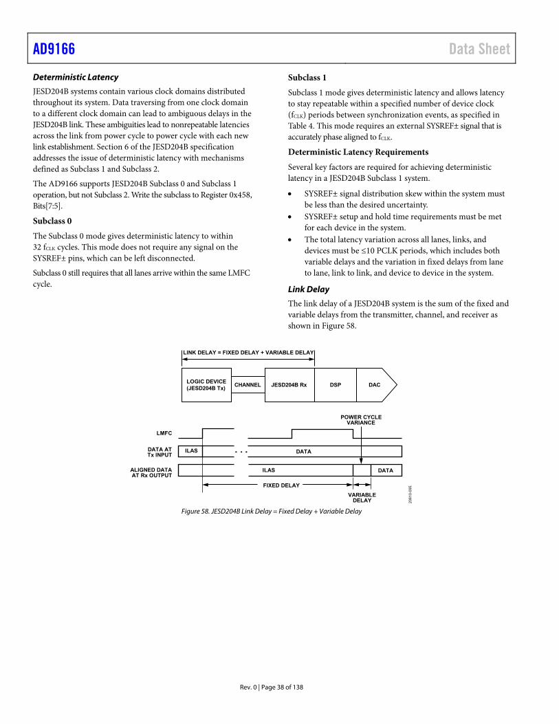
AD9166 Data Sheet
Rev. 0 | Page 38 of 138
Deterministic Latency
JESD204B systems contain various clock domains distributed throughout its system. Data traversing from one clock domain to a different clock domain can lead to ambiguous delays in the JESD204B link. These ambiguities lead to nonrepeatable latencies across the link from power cycle to power cycle with each new link establishment. Section 6 of the JESD204B specification addresses the issue of deterministic latency with mechanisms defined as Subclass 1 and Subclass 2.
The AD9166 supports JESD204B Subclass 0 and Subclass 1 operation, but not Subclass 2. Write the subclass to Register 0x458, Bits[7:5].
Subclass 0
The Subclass 0 mode gives deterministic latency to within 32 fCLK cycles. This mode does not require any signal on the SYSREF± pins, which can be left disconnected.
Subclass 0 still requires that all lanes arrive within the same LMFC cycle.
Subclass 1
Subclass 1 mode gives deterministic latency and allows latency to stay repeatable within a specified number of device clock (fCLK) periods between synchronization events, as specified in Table 4. This mode requires an external SYSREF± signal that is accurately phase aligned to fCLK.
Deterministic Latency Requirements
Several key factors are required for achieving deterministic latency in a JESD204B Subclass 1 system.
SYSREF± signal distribution skew within the system must be less than the desired uncertainty.
SYSREF± setup and hold time requirements must be met for each device in the system.
The total latency variation across all lanes, links, and devices must be ≤10 PCLK periods, which includes both variable delays and the variation in fixed delays from lane to lane, link to link, and device to device in the system.
Link Delay
The link delay of a JESD204B system is the sum of the fixed and variable delays from the transmitter, channel, and receiver as shown in Figure 58.
ILAS
ILAS
FIXED DELAYVARIABLE
DELAY
POWER CYCLEVARIANCE
DATA
LMFC
ALIGNED DATAAT Rx OUTPUT
DATA ATTx INPUT DATA
DSPCHANNELLOGIC DEVICE(JESD204B Tx) JESD204B Rx DAC
LINK DELAY = FIXED DELAY + VARIABLE DELAY
2081
0-09
5
Figure 58. JESD204B Link Delay = Fixed Delay + Variable Delay
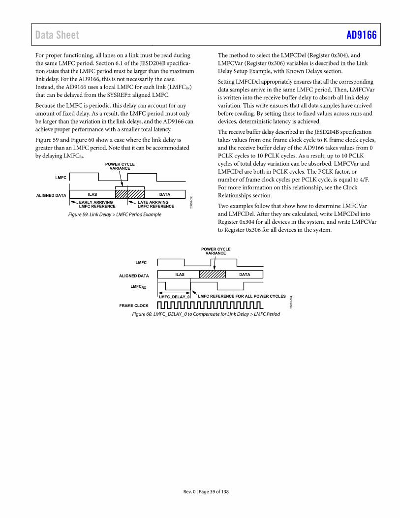
Data Sheet AD9166
Rev. 0 | Page 39 of 138
For proper functioning, all lanes on a link must be read during the same LMFC period. Section 6.1 of the JESD204B specifica-tion states that the LMFC period must be larger than the maximum link delay. For the AD9166, this is not necessarily the case. Instead, the AD9166 uses a local LMFC for each link (LMFCRx) that can be delayed from the SYSREF± aligned LMFC.
Because the LMFC is periodic, this delay can account for any amount of fixed delay. As a result, the LMFC period must only be larger than the variation in the link delays, and the AD9166 can achieve proper performance with a smaller total latency.
Figure 59 and Figure 60 show a case where the link delay is greater than an LMFC period. Note that it can be accommodated by delaying LMFCRx.
ILAS DATA
POWER CYCLEVARIANCE
LMFC
ALIGNED DATAEARLY ARRIVINGLMFC REFERENCE
LATE ARRIVINGLMFC REFERENCE 20
810-
093
Figure 59. Link Delay > LMFC Period Example
The method to select the LMFCDel (Register 0x304), and LMFCVar (Register 0x306) variables is described in the Link Delay Setup Example, with Known Delays section.
Setting LMFCDel appropriately ensures that all the corresponding data samples arrive in the same LMFC period. Then, LMFCVar is written into the receive buffer delay to absorb all link delay variation. This write ensures that all data samples have arrived before reading. By setting these to fixed values across runs and devices, deterministic latency is achieved.
The receive buffer delay described in the JESD204B specification takes values from one frame clock cycle to K frame clock cycles, and the receive buffer delay of the AD9166 takes values from 0 PCLK cycles to 10 PCLK cycles. As a result, up to 10 PCLK cycles of total delay variation can be absorbed. LMFCVar and LMFCDel are both in PCLK cycles. The PCLK factor, or number of frame clock cycles per PCLK cycle, is equal to 4/F. For more information on this relationship, see the Clock Relationships section.
Two examples follow that show how to determine LMFCVar and LMFCDel. After they are calculated, write LMFCDel into Register 0x304 for all devices in the system, and write LMFCVar to Register 0x306 for all devices in the system.
ILAS DATA
FRAME CLOCK
POWER CYCLEVARIANCE
LMFC
ALIGNED DATA
LMFCRX
LMFC_DELAY_0 LMFC REFERENCE FOR ALL POWER CYCLES20
810-
094
Figure 60. LMFC_DELAY_0 to Compensate for Link Delay > LMFC Period
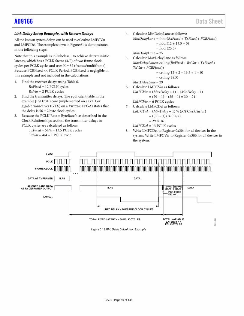
AD9166 Data Sheet
Rev. 0 | Page 40 of 138
Link Delay Setup Example, with Known Delays
All the known system delays can be used to calculate LMFCVar and LMFCDel. The example shown in Figure 61 is demonstrated in the following steps.
Note that this example is in Subclass 1 to achieve deterministic latency, which has a PCLK factor (4/F) of two frame clock cycles per PCLK cycle, and uses K = 32 (frames/multiframe). Because PCBFixed << PCLK Period, PCBFixed is negligible in this example and not included in the calculations.
1. Find the receiver delays using Table 6. RxFixed = 12 PCLK cycles RxVar = 2 PCLK cycles
2. Find the transmitter delays. The equivalent table in the example JESD204B core (implemented on a GTH or gigabit transceiver (GTX) on a Virtex-6 FPGA) states that the delay is 56 ± 2 byte clock cycles.
3. Because the PCLK Rate = ByteRate/4 as described in the Clock Relationships section, the transmitter delays in PCLK cycles are calculated as follows:
TxFixed = 54/4 = 13.5 PCLK cycles TxVar = 4/4 = 1 PCLK cycle
4. Calculate MinDelayLane as follows: MinDelayLane = floor(RxFixed + TxFixed + PCBFixed) = floor(12 + 13.5 + 0) = floor(25.5) MinDelayLane = 25
5. Calculate MaxDelayLane as follows: MaxDelayLane = ceiling(RxFixed + RxVar + TxFixed + TxVar + PCBFixed)) = ceiling(12 + 2 + 13.5 + 1 + 0) = ceiling(28.5) MaxDelayLane = 29
6. Calculate LMFCVar as follows: LMFCVar = (MaxDelay + 1) − (MinDelay − 1) = (29 + 1) − (25 − 1) = 30 − 24 LMFCVar = 6 PCLK cycles
7. Calculate LMFCDel as follows: LMFCDel = (MinDelay − 1) % (K/PClockFactor) = ((30 − 1)) % (32/2) = 29 % 16 LMFCDel = 13 PCLK cycles
8. Write LMFCDel to Register 0x304 for all devices in the system. Write LMFCVar to Register 0x306 for all devices in the system.
FRAME CLOCK
LMFC
PCLK
DATADATA AT Tx FRAMER ILAS
LMFCRX
TOTAL FIXED LATENCY = 30 PCLK CYCLES
LMFC DELAY = 26 FRAME CLOCK CYCLES
PCB FIXEDDELAY
DATAALIGNED LANE DATAAT Rx DEFRAMER OUTPUT ILAS
TOTAL VARIABLELATENCY = 4
PCLK CYCLES
Tx VARDELAY
Rx VARDELAY
2081
0-09
6
Figure 61. LMFC Delay Calculation Example
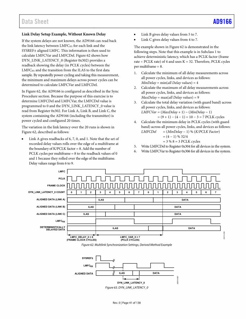
Data Sheet AD9166
Rev. 0 | Page 41 of 138
Link Delay Setup Example, Without Known Delay
If the system delays are not known, the AD9166 can read back the link latency between LMFCRX for each link and the SYSREF± aligned LMFC. This information is then used to calculate LMFCVar and LMFCDel. Figure 62 shows how DYN_LINK_LATENCY_0 (Register 0x302) provides a readback showing the delay (in PCLK cycles) between the LMFCRX and the transition from the ILAS to the first data sample. By repeatedly power cycling and taking this measurement, the minimum and maximum delays across power cycles can be determined to calculate LMFCVar and LMFCDel.
In Figure 62, the AD9166 is configured as described in the Sync Procedure section. Because the purpose of this exercise is to determine LMFCDel and LMFCVar, the LMFCDel value is programmed to 0 and the DYN_LINK_LATENCY_0 value is read from Register 0x302. For Link A, Link B, and Link C, the system containing the AD9166 (including the transmitter) is power cycled and configured 20 times.
The variation in the link latency over the 20 runs is shown in Figure 62, described as follows:
Link A gives readbacks of 6, 7, 0, and 1. Note that the set of recorded delay values rolls over the edge of a multiframe at the boundary of K/PCLK factor = 8. Add the number of PCLK cycles per multiframe = 8 to the readback values of 0 and 1 because they rolled over the edge of the multiframe. Delay values range from 6 to 9.
Link B gives delay values from 5 to 7. Link C gives delay values from 4 to 7.
The example shown in Figure 62 is demonstrated in the following steps. Note that this example is in Subclass 1 to achieve deterministic latency, which has a PCLK factor (frame rate ÷ PCLK rate) of 4 and uses K = 32. Therefore, PCLK cycles per multiframe = 8.
1. Calculate the minimum of all delay measurements across all power cycles, links, and devices as follows: MinDelay = min(all Delay values) = 4
2. Calculate the maximum of all delay measurements across all power cycles, links, and devices as follows: MaxDelay = max(all Delay values) = 9
3. Calculate the total delay variation (with guard band) across all power cycles, links, and devices as follows: LMFCVar = (MaxDelay + 1) − (MinDelay − 1) = (9 + 1) − (4 − 1) = 10 − 3 = 7 PCLK cycles
4. Calculate the minimum delay in PCLK cycles (with guard band) across all power cycles, links, and devices as follows: LMFCDel = (MinDelay − 1) % (K/PCLK Factor) = (4 − 1) % 32/4 = 3 % 8 = 3 PCLK cycles
5. Write LMFCDel to Register 0x304 for all devices in the system. 6. Write LMFCVar to Register 0x306 for all devices in the system.
0 1 2 3 4 5 6 7 0 1 2 3 4 5 6 7DYN_LINK_LATENCY_0 COUNT
ALIGNED DATA (LINK A)
DETERMINISTICALLYDELAYED DATA
LMFCRX
ALIGNED DATA (LINK B)
ALIGNED DATA (LINK C)
FRAME CLOCK
LMFC
PCLK
DATAILAS
DATAILAS
DATAILAS
DATAILAS
LMFC_DELAY_0 = 6(FRAME CLOCK CYCLES)
LMFC_VAR_0 = 7(PCLK CYCLES) 20
810-
098
Figure 62. Multilink Synchronization Settings, Derived Method Example
ILAS DATA
SYSREF±
ALIGNED DATA
LMFCRX
DYN_LINK_LATENCY_0 2081
0-09
7
Figure 63. DYN_LINK_LATENCY_0
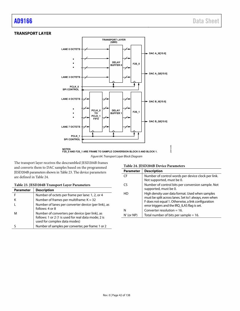
AD9166 Data Sheet
Rev. 0 | Page 42 of 138
TRANSPORT LAYER
DELAYBUFFER 1
DELAYBUFFER 0 F2S_0
F2S_1
DAC A_I0[15:0]
DAC A_Q0[15:0]
PCLK_1
LANE 0 OCTETS
LANE 7 OCTETS
PCLK_0SPI CONTROL
LANE 3 OCTETS
LANE 4 OCTETSDAC B_I0[15:0]
DAC B_Q0[15:0]
TRANSPORT LAYER(QBD)
SPI CONTROL
PCLK_0TO
PCLK_1FIFO
2081
0-09
9
NOTESF2S_0 AND F2S_1 ARE FRAME TO SAMPLE CONVERSION BLOCK 0 AND BLOCK 1.
Figure 64. Transport Layer Block Diagram
The transport layer receives the descrambled JESD204B frames and converts them to DAC samples based on the programmed JESD204B parameters shown in Table 23. The device parameters are defined in Table 24.
Table 23. JESD204B Transport Layer Parameters Parameter Description F Number of octets per frame per lane: 1, 2, or 4 K Number of frames per multiframe: K = 32 L Number of lanes per converter device (per link), as
follows: 4 or 8 M Number of converters per device (per link), as
follows: 1 or 2 (1 is used for real data mode; 2 is used for complex data modes)
S Number of samples per converter, per frame: 1 or 2
Table 24. JESD204B Device Parameters Parameter Description CF Number of control words per device clock per link.
Not supported, must be 0. CS Number of control bits per conversion sample. Not
supported, must be 0. HD High density user data format. Used when samples
must be split across lanes. Set to1 always, even when F does not equal 1. Otherwise, a link configuration error triggers and the IRQ_ILAS flag is set.
N Converter resolution = 16. N' (or NP) Total number of bits per sample = 16.
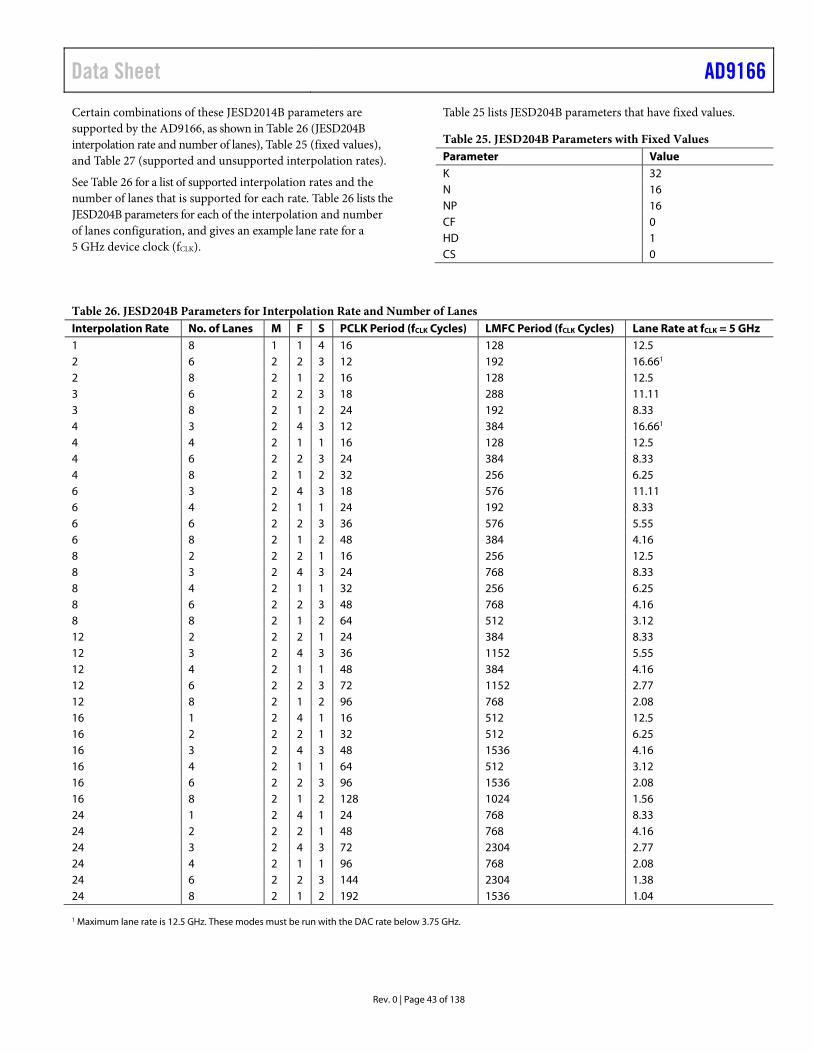
Data Sheet AD9166
Rev. 0 | Page 43 of 138
Certain combinations of these JESD2014B parameters are supported by the AD9166, as shown in Table 26 (JESD204B interpolation rate and number of lanes), Table 25 (fixed values), and Table 27 (supported and unsupported interpolation rates).
See Table 26 for a list of supported interpolation rates and the number of lanes that is supported for each rate. Table 26 lists the JESD204B parameters for each of the interpolation and number of lanes configuration, and gives an example lane rate for a 5 GHz device clock (fCLK).
Table 25 lists JESD204B parameters that have fixed values.
Table 25. JESD204B Parameters with Fixed Values Parameter Value K 32 N 16 NP 16 CF 0 HD 1 CS 0
Table 26. JESD204B Parameters for Interpolation Rate and Number of Lanes Interpolation Rate No. of Lanes M F S PCLK Period (fCLK Cycles) LMFC Period (fCLK Cycles) Lane Rate at fCLK = 5 GHz 1 8 1 1 4 16 128 12.5 2 6 2 2 3 12 192 16.661 2 8 2 1 2 16 128 12.5 3 6 2 2 3 18 288 11.11 3 8 2 1 2 24 192 8.33 4 3 2 4 3 12 384 16.661 4 4 2 1 1 16 128 12.5 4 6 2 2 3 24 384 8.33 4 8 2 1 2 32 256 6.25 6 3 2 4 3 18 576 11.11 6 4 2 1 1 24 192 8.33 6 6 2 2 3 36 576 5.55 6 8 2 1 2 48 384 4.16 8 2 2 2 1 16 256 12.5 8 3 2 4 3 24 768 8.33 8 4 2 1 1 32 256 6.25 8 6 2 2 3 48 768 4.16 8 8 2 1 2 64 512 3.12 12 2 2 2 1 24 384 8.33 12 3 2 4 3 36 1152 5.55 12 4 2 1 1 48 384 4.16 12 6 2 2 3 72 1152 2.77 12 8 2 1 2 96 768 2.08 16 1 2 4 1 16 512 12.5 16 2 2 2 1 32 512 6.25 16 3 2 4 3 48 1536 4.16 16 4 2 1 1 64 512 3.12 16 6 2 2 3 96 1536 2.08 16 8 2 1 2 128 1024 1.56 24 1 2 4 1 24 768 8.33 24 2 2 2 1 48 768 4.16 24 3 2 4 3 72 2304 2.77 24 4 2 1 1 96 768 2.08 24 6 2 2 3 144 2304 1.38 24 8 2 1 2 192 1536 1.04 1 Maximum lane rate is 12.5 GHz. These modes must be run with the DAC rate below 3.75 GHz.
AD9166 Data Sheet
Rev. 0 | Page 44 of 138
A value of yes in Table 27 means the interpolation rate is supported for the number of lanes. A blank cell means it is not supported.
Table 27. Interpolation Rates and Number of Lanes Interpolation 8 6 4 3 2 1 1× Yes1 2× Yes Yes1 3× Yes Yes 4× Yes Yes Yes Yes1 6× Yes Yes Yes Yes 8× Yes Yes Yes Yes Yes 12× Yes Yes Yes Yes Yes 16× Yes Yes Yes Yes Yes Yes 24× Yes Yes Yes Yes Yes Yes 1 These modes restrict the maximum device clock rate to 5 GHz.
Configuration Parameters
The AD9166 modes refer to the link configuration parameters for L, K, M, N, NP, S, and F. Table 28 provides the description and addresses for these settings.
Table 28. Configuration Parameters JESD204B Setting Description Address L − 1 Number of lanes minus 1. Register 0x453,
Bits[4:0] F − 1 Number of ((octets per frame) per
lane) minus 1. Register 0x454, Bits[7:0]
K − 1 Number of frames per multiframe minus 1.
Register 0x455, Bits[4:0]
M − 1 Number of converters minus 1. Register 0x456, Bits[7:0]
N − 1 Converter bit resolution minus 1. Register 0x457, Bits[4:0]
NP − 1 Bit packing per sample minus 1. Register 0x458, Bits[4:0]
S − 1 Number of ((samples per converter) per frame) minus 1.
Register 0x459, Bits[4:0]
HD High density format. Set to 1 if F = 1. Leave at 0 if F ≠ 1.
Register 0x45A, Bit 7
DID Device ID. Match the device ID sent by the transmitter.
Register 0x450, Bits[7:0]
BID Bank ID. Match the bank ID sent by the transmitter.
Register 0x451, Bits[7:0]
LID0 Lane ID for Lane 0. Match the Lane ID sent by the transmitter on Logical Lane 0.
Register 0x452, Bits[4:0]
JESDV JESD204x version. Match the version sent by the transmitter (0x0 = JESD204A, 0x1 = JESD204B).
Register 0x459, Bits[7:5]
Data Flow Through the JESD204B Receiver
The link configuration parameters determine how the serial bits on the JESD204B receiver interface are deframed and passed on to the DACs as data samples.
Deskewing and Enabling Logical Lanes
After proper configuration, the logical lanes are automatically deskewed. All logical lanes are enabled or not based on the lane number setting in Register 0x110, Bits[7:4]. The physical lanes are all powered up by default.
To disable power to physical lanes that are not being used, set Bit x in Register 0x201 to 1 to disable Physical Lane x, and keep it at 0 to enable it.
JESD204B TEST MODES PHY PRBS Testing
The JESD204B receiver on the AD9166 includes a pseudorandom binary sequence (PRBS) pattern checker on the back end of its physical layer. This functionality enables bit error rate (BER) testing of each physical lane of the JESD204B link. The PHY PRBS pattern checker does not require that the JESD204B link be established. The pattern checker can synchronize with a PRBS7, PRBS15, or PRBS31 data pattern. The PRBS pattern can be verified on multiple lanes simultaneously. The error counts for failing lanes are reported for one JESD204B lane at a time.
Table 29. PHY PRBS Pattern Selection PHY_PRBS_PAT_SEL Setting (Register 0x316, Bits[3:2]) PRBS Pattern 0b00 (default) PRBS7 0b01 PRBS15 0b10 PRBS31
The process for performing PRBS testing on the AD9166 is as follows, using Table 29 for reference.
1. Start sending a PRBS7, PRBS15, or PRBS31 pattern from the JESD204B transmitter.
2. Select and write the appropriate PRBS pattern to Register 0x316, Bits[3:2], as shown in Table 29.
3. Enable the PHY test for all lanes being tested by writing to PHY_TEST_EN (Register 0x315). Each bit of Register 0x315 enables the PRBS test for the corresponding lane. For example, writing a 1 to Bit 0 enables the PRBS test for Physical Lane 0.
4. Toggle PHY_TEST_RESET (Register 0x316, Bit 0) from 0 to 1 then back to 0.
5. Set PHY_PRBS_TEST_THRESHOLD_xBITS (Bits[23:0], Register 0x319 to Register 0x317) as desired.
6. Write a 0 and then a 1 to PHY_TEST_START (Register 0x316, Bit 1). The rising edge of PHY_TEST_START starts the test. a. (Optional) In some cases, it may be necessary to
repeat Step 4 at this point. Toggle PHY_TEST_RESET (Register 0x316, Bit 0) from 0 to 1, then back to 0.
7. Wait 500 ms. 8. Stop the test by writing PHY_TEST_START
(Register 0x316, Bit 1) = 0.
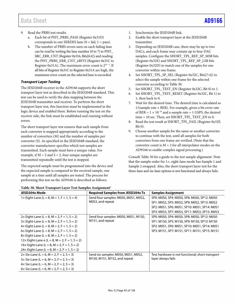
Data Sheet AD9166
Rev. 0 | Page 45 of 138
9. Read the PRBS test results. a. Each bit of PHY_PRBS_PASS (Register 0x31D)
corresponds to one SERDES lane (0 = fail, 1 = pass). b. The number of PRBS errors seen on each failing lane
can be read by writing the lane number (0 to 7) to PHY_ SRC_ERR_CNT (Register 0x316, Bits[6:4]) and reading the PHY_PRBS_ERR_CNT_xBITS (Register 0x31C to Register 0x31A). The maximum error count is 224 − 1. If all bits of Register 0x31C to Register 0x31A are high, the maximum error count on the selected lane is exceeded.
Transport Layer Testing
The JESD204B receiver in the AD9166 supports the short transport layer test as described in the JESD204B standard. This test can be used to verify the data mapping between the JESD204B transmitter and receiver. To perform the short transport layer test, this function must be implemented in the logic device and enabled there. Before running the test on the receiver side, the link must be established and running without errors.
The short transport layer test ensures that each sample from each converter is mapped appropriately according to the number of converters (M) and the number of samples per converter (S). As specified in the JESD204B standard, the converter manufacturer specifies which test samples are transmitted. Each sample must have a unique value. For example, if M = 2 and S = 2, four unique samples are transmitted repeatedly until the test is stopped.
The expected sample must be programmed into the device and the expected sample is compared to the received sample, one sample at a time until all samples are tested. The process for performing this test on the AD9166 is described as follows:
1. Synchronize the JESD204B link. 2. Enable the short transport layer at the JESD204B
transmitter. 3. Depending on JESD204B case, there may be up to two
DACs, and each frame may contain up to four DAC samples. Configure the SHORT_TPL_REF_SP_MSB bits (Register 0x32E) and SHORT_TPL_REF_SP_LSB bits (Register 0x32D) to match one of the samples for one converter within one frame.
4. Set SHORT_TPL_SP_SEL (Register 0x32C, Bits[7:4]) to select the sample within one frame for the selected converter according to Table 30.
5. Set SHORT_TPL_TEST_EN (Register 0x32C, Bit 0) to 1. 6. Set SHORT_TPL_TEST_RESET (Register 0x32C, Bit 1) to
1, then back to 0. 7. Wait for the desired time. The desired time is calculated as
1/(sample rate × BER). For example, given a bit error rate of BER = 1 × 10⁻¹⁰ and a sample rate = 1 GSPS, the desired time = 10 sec. Then, set SHORT_TPL_TEST_EN to 0.
8. Read the test result at SHORT_TPL_FAIL (Register 0x32F, Bit 0).
9. Choose another sample for the same or another converter to continue with the test, until all samples for both converters from one frame are verified. (Note that the converter count is M = 2 for all interpolator modes on the AD9166 to enable complex signal processing.)
Consult Table 30 for a guide to the test sample alignment. Note that the sample order for 1×, eight-lane mode has Sample 1 and Sample 2 swapped. Also, the short transport layer test for the three-lane and six-lane options is not functional and always fails.
Table 30. Short Transport Layer Test Samples Assignment1 JESD204x Mode Required Samples from JESD204x Tx Samples Assignment 1× Eight-Lane (L = 8, M = 1, F = 1, S = 4) Send four samples: M0S0, M0S1, M0S2,
M0S3, and repeat SP0: M0S0, SP4: M0S0, SP8: M0S0, SP12: M0S0
SP1: M0S2, SP5: M0S2, SP9: M0S2, SP13: M0S2 SP2: M0S1, SP6: M0S1, SP10: M0S1, SP14: M0S1 SP3: M0S3, SP7: M0S3, SP11: M0S3, SP15: M0S3 2× Eight-Lane (L = 8, M = 2, F = 1, S = 2) Send four samples: M0S0, M0S1, M1S0,
M1S1, and repeat SP0: M0S0, SP4: M0S0, SP8: M0S0, SP12: M0S0
3× Eight-Lane (L = 8, M = 2, F = 1, S = 2) SP1: M1S0, SP5: M1S0, SP9: M1S0, SP13: M1S0 4× Eight-Lane (L = 8, M = 2, F = 1, S = 2) SP2: M0S1, SP6: M0S1, SP10: M0S1, SP14: M0S1 6× Eight-Lane (L = 8, M = 2, F = 1, S = 2) SP3: M1S1, SP7: M1S1, SP11: M1S1, SP15: M1S1 8× Eight-Lane (L = 8, M = 2, F = 1, S = 2) 12× Eight-Lane e (L = 8, M = 2, F = 1, S = 2) 16× Eight-Lane (L = 8, M = 2, F = 1, S = 2) 24× Eight-Lane (L = 8, M = 2, F = 1, S = 2) 2× Six-Lane (L = 6, M = 2, F = 2, S = 3) Send six samples: M0S0, M0S1, M0S2,
M1S0, M1S1, M1S2, and repeat Test hardware is not functional; short transport layer always fails 3× Six-Lane (L = 6, M = 2, F = 2, S = 3)
4× Six-Lane (L = 6, M = 2, F = 2, S = 3) 6× Six-Lane (L = 6, M = 2, F = 2, S = 3)
AD9166 Data Sheet
Rev. 0 | Page 46 of 138
JESD204x Mode Required Samples from JESD204x Tx Samples Assignment 8× Six-Lane (L = 6, M = 2, F = 2, S = 3) 12× Six-Lane (L = 6, M = 2, F = 2, S = 3) 16× Six-Lane (L = 6, M = 2, F = 2, S = 3) 24× Six-Lane (L = 6, M = 2, F = 2, S = 3) 4× Three-Lane (L = 3, M = 2, F = 4, S = 3) 6× Three-Lane (L = 3, M = 2, F = 4, S = 3) 8× Three-Lane (L = 3, M = 2, F = 4, S = 3) 12× Three-Lane (L = 3, M = 2, F = 4, S = 3) 16× Three-Lane (L = 3, M = 2, F = 4, S = 3) 24× Three-Lane (L = 3, M = 2, F = 4, S = 3) 4× Four-Lane (L = 4, M = 2, F = 1, S = 1) Send two samples: M0S0, M1S0, repeat SP0: M0S0, SP4: M0S0, SP8: M0S0, SP12: M0S0 6× Four-Lane (L = 4, M = 2, F = 1, S = 1) SP1: M1S0, SP5: M1S0, SP9: M1S0, SP13: M1S0 8× Four-Lane (L = 4, M = 2, F = 1, S = 1) SP2: M0S0, SP6: M0S0, SP10: M0S0, SP14: M0S0 12× Four-Lane (L = 4, M = 2, F = 1, S = 1) SP3: M1S0, SP7: M1S0, SP11: M1S0, SP15: M1S0 16× Four-Lane (L = 4, M = 2, F = 1, S = 1) 24× Four-Lane (L = 4, M = 2, F = 1, S = 1) 8× Two-Lane (L = 2, M = 2, F = 2, S = 1) 12× Two-Lane (L = 2, M = 2, F = 2, S = 1) 16× Two-Lane (L = 2, M = 2, F = 2, S = 1) 24× Two-Lane (L = 2, M = 2, F = 2, S = 1) 16× One-Lane (L = 1, M = 2, F = 4, S = 1) 24× One-Lane (L = 1, M = 2, F = 4, S = 1)
1 Mx is the converter number and Sy is the sample number. For example, M0S0 means Converter 0, Sample 0. SPx is the sample pattern word number. For example, SP0 means Sample Pattern Word 0.
Repeated CGS and ILAS Test
As per Section 5.3.3.8.2 of the JESD204B specification, the AD9166 can check that a constant stream of /K28.5/ characters is being received, or that code group synchronization (CGS) followed by a constant stream of ILAS is being received.
To run a repeated CGS test, send a constant stream of /K28.5/ characters to the AD9166 SERDES inputs. Next, set up the device and enable the links. Ensure that the /K28.5/ characters are being received by verifying that SYNCOUT± is deasserted and that CGS has passed for all enabled link lanes by reading Register 0x470.
To run the CGS followed by a repeated ILAS sequence test, follow the procedure to set up the links. However, before performing the last write (enabling the links), enable the ILAS test mode by writing a 1 to Register 0x477, Bit 7. Then, enable the links. When the device recognizes four CGS characters on each lane, it desserts the SYNCOUT±. At this point, the transmitter starts sending a repeated ILAS sequence.
Read Register 0x473 to verify that initial lane synchronization has passed for all enabled link lanes.
JESD204B ERROR MONITORING Disparity, Not in Table, and Unexpected Control (K) Character Errors
As per Section 7.6 of the JESD204B specification, the AD9166 can detect disparity errors, not in table (NIT) errors, and unexpected control (K) character errors, and can optionally issue a sync request and reinitialize the link when errors occur.
Note that the disparity error counter counts all characters with invalid disparity, regardless of whether they are in the 8-bit/10-bit decoding table. This error counting method is a minor deviation from the JESD204B specification, which only counts disparity errors when they are in the 8-bit/10-bit decoding table.
Several other interpretations of the JESD204B specification are noted in this section. When three NIT errors are injected to one lane and QUAL_RDERR (Register 0x476, Bit 4) = 1, the readback values of the bad disparity error (BDE) count register is 1. Reporting of disparity errors that occur at the same character position of a NIT error is disabled. No such disabling is performed for the disparity errors in the characters after a NIT error. Therefore, it is expected behavior that a NIT error may result in a BDE error.
A resync is triggered when four NIT errors are injected with Register 0x476, Bit 4 = 1. When this bit is set, the error counter does not distinguish between a concurrent invalid symbol with the wrong running disparity but is in the 8-bit/10-bit decoding table, and a NIT error. Thus, a resync can be triggered when
Data Sheet AD9166
Rev. 0 | Page 47 of 138
four NIT errors are injected because they are not distinguished from disparity errors.
Checking Error Counts
The error count can be checked for BDEs, NIT errors, and unexpected K (UEK) character errors. The error counts are on a per lane and per error type basis. Each error type and lane has a register dedicated to it. To check the error count, the following steps must be performed:
1. Choose and enable the type of errors to monitor by selecting them in Register 0x480, Bits[5:3] to Register 0x487, Bits[5:3]. UEK, BDE, and NIT error monitoring can be selected for each lane by writing a 1 to the appropriate bit, as described in the register map. These bits are enabled by default.
2. The corresponding error counter reset bits are in Register 0x480, Bits[2:0] to Register 0x487, Bits[2:0]. Write a 0 to the corresponding bit to reset that error counter.
3. Registers 0x488, Bits[2:0] to Register 0x48F, Bits[2:0] have the terminal count hold indicator for each error counter. If this flag is enabled, when the terminal error count of 0xFF is reached, the counter ceases counting and holds that value until reset. Otherwise, it wraps to 0x00 and continues counting. Select the desired behavior, and program the corresponding register bits per lane.
Check for Error Count Overthreshold
To check for the error count over threshold, follow these steps:
1. Define the error counter threshold. The error counter threshold can be set to a user defined value in Register 0x47C, or remain at the default value of 0xFF. When the error threshold is reached, an IRQ is generated, SYNCOUT± is asserted, or both, depending on the mask register settings. This single error threshold is used for all three types of errors (UEK, NIT, and BDE).
2. Set the SYNC_ASSERT_MASK bits. The SYNCOUT± assertion behavior is set in Register 0x47D, Bits[2:0]. By default, when any error counter of any lane is equal to the threshold, it asserts SYNCOUT± (Register 0x47D, Bits[2:0] = 0b111).
3. Read the indicator for error count reached. Each error counter has an indicator for when a terminal count is reached, per lane. This indicator is set to 1 when the terminal count of an error counter for a particular lane has been reached. These status bits are located in Register 0x490, Bits[2:0] to Register 0x497, Bits[2:0]. These registers also indicate whether a particular lane is active by setting Bit 3 = 0b1.
Error Counter and Interrupt Request Control
For error counter and interrupt request control, follow these steps:
1. Enable the interrupts. Enable the JESD204B interrupts. The interrupts for the UEK, NIT, and BDE error counters are in Register 0x4B8, Bits[7:5]. There are other interrupts to monitor when bringing up the link, such as interlane deskewing, initial lane sync, good check sum, frame sync, code group sync (Register 0x4B8, Bits[4:0]), and configuration mismatch (Register 0x4B9, Bit 0). These bits are off by default but can be enabled by writing 0b1 to the corresponding bit.
2. Read the JESD204B interrupt status. The interrupt status bits are in Register 0x4BA, Bits[7:0] and Register 0x4BB, Bit 0, with the status bit position corresponding to the enable bit position.
3. It is recommended to enable all interrupts that are planned to be used prior to bringing up the JESD204B link. When the link is up, the interrupts can be reset and then used to monitor the link status.
Monitoring Errors via SYNCOUT±
As per the JESD204B specifications, when one or more BDE, NIT, or unexpected control character (including UEK) errors occur, the error is reported on the SYNCOUT± pin by asserting the SYNCOUT± signal for exactly two frame periods. For the AD9166, the width of the SYNCOUT± pulse can be programmed to ½, 1, or 2 PCLK cycles. The settings to achieve a SYNCOUT± pulse of two frame clock cycles are listed in Table 31.
Table 31. Setting SYNCOUT± Error Pulse Duration
1 F is a link configuration parameter (see Table 28). 2 These register settings assert the SYNCOUT± signal for two frame clock cycle
pulse widths.
UEK, NIT, and BDE IRQs
For UEK, NIT, and BDE errors, error count overthreshold events are available as IRQ events. Enable these events by writing to Register 0x4B8, Bits[7:5]. After the IRQs are enabled, the IRQ event status can be read at Register 0x4BA, Bits[7:5].
See the Interrupt Request Operation section for more information on IRQs and see the Error Counter and Interrupt Request Control section for information on resetting the IRQ.
F1 PCLK Factor (Frames per PCLK)
SYNC_ERR_DUR (Register 0x312, Bits[7:4]) Setting2
1 4 0 (default) 2 2 1 4 1 2
AD9166 Data Sheet
Rev. 0 | Page 48 of 138
Errors Requiring Reinitializing
A link reinitialization automatically occurs when four invalid disparity characters are received per the JESD204B specification. When a link reinitialization occurs, the resync request is five frames and nine octets long.
The user can optionally reinitialize the link when the error count for disparity errors, NIT errors, or UEK character errors reaches a programmable error threshold. The process to enable the reinitialization feature for certain error types is as follows:
1. Choose and enable which errors to monitor by selecting them in Register 0x480, Bits[5:3] to Register 0x487, Bits[5:3]. UEK, BDE, and NIT error monitoring can be selected for each lane by writing a 1 to the appropriate bit, as described in Table 46. These bits are enabled by default.
2. Enable the sync assertion mask for each type of error by writing to SYNC_ASSERT_MASK (Register 0x47D, Bits[2:0]) according to Table 32.
3. Program the desired error counter threshold into ERRORTHRES (Register 0x47C).
4. For each error type enabled in the SYNC_ASSERT_MASK register, if the error counter on any lane reaches the programmed threshold, SYNCOUT± falls, issuing a sync request. Note that all error counts are reset when a link reinitialization occurs. The IRQ does not reset and must be reset manually.
Table 32. Sync Assertion Mask (SYNC_ASSERT_MASK, Address 0x47D) Bit No. Bit Name Description 2 UEK Set to 1 to assert SYNCOUT± if the UEK
character error count reaches the threshold
1 NIT Set to 1 to assert SYNCOUT± if the NIT error count reaches the threshold
0 BDE Set to 1 to assert SYNCOUT± if the disparity error count reaches the threshold
CGS, Frame Sync, Checksum, and ILAS Monitoring
Monitor Register 0x470 to Register 0x473 to verify that each stage of the JESD204B link establishment has occurred.
Bit x of CODE_GRP_SYNC (Register 0x470) is high if Link Lane x received at least four K28.5 characters and passed CGS.
Bit x of FRAME_SYNC (Register 0x471) is high if Link Lane x completed initial frame synchronization.
Bit x of GOOD_CHECKSUM (Register 0x472) is high if the checksum sent over the lane matches the sum of the JESD204B parameters sent over the lane during ILAS for Link Lane x. The parameters can be added either by summing the individual fields in registers or summing the packed register. If Register 0x300, Bit 6 = 0 (default), the calculated checksums are the lower eight bits of the sum of the following fields: DID, BID, LIDx, SCR, L − 1, F − 1, K − 1, M − 1, N − 1, SUBCLASSV, NP − 1, JESDV, S − 1, and HD. If Register 0x300, Bit 6 = 1, the calculated checksums are the lower eight bits of the sum of Register 0x400 to Register 0x40C and LIDx, where x refers to a Link Lane x.
Bit x of INIT_LANE_SYNC (Register 0x473) is high if Link Lane x passed the initial lane alignment sequence.
CGS, Frame Sync, Checksum, and ILAS IRQs
Fail signals for CGS, frame sync, checksum, and ILAS are available as IRQ events. Enable them by writing to Register 0x4B8, Bits[3:0]. The IRQ event status can be read at Register 0x4BA, Bits[3:0] after the IRQs are enabled.
Write a 1 to Register 0x4BA, Bit 0 to reset the CGS IRQ. Write a 1 to Register 0x4BA, Bit 1 to reset the frame sync IRQ. Write a 1 to Register 0x4BA, Bit 2 to reset the checksum IRQ. Write a 1 to Register 0x4BA, Bit 3 to reset the ILAS IRQ.
See the Interrupt Request Operation section for more information.
Configuration Mismatch IRQ
The AD9166 has a configuration mismatch flag that is available as an IRQ event. Use Register 0x4B9, Bit 0 to enable the mismatch flag (it is enabled by default), and then use Register 0x4BB, Bit 0 to read back its status and reset the IRQ signal. See the Interrupt Request Operation section for more information.
The configuration mismatch event flag is high when the link configuration settings (in Register 0x450 to Register 0x45D) do not match the JESD204B transmitted settings (Register 0x400 to Register 0x40D).
This function is different from the good checksum flags in Register 0x472. The good checksum flags ensure that the transmit-ted checksum matches a calculated checksum based on the transmitted settings. The configuration mismatch event ensures that the transmitted settings match the configured settings.
HARDWARE CONSIDERATIONS See the Applications Information section for information on hardware considerations.
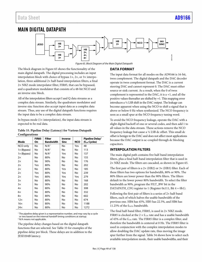
Data Sheet AD9166
Rev. 0 | Page 49 of 138
MAIN DIGITAL DATAPATH
HB2×
HB3×
JESD
HB2×,4×,8×
NCO INVSINC
HB2×
2081
0-20
4
Figure 65. Block Diagram of the Main Digital Datapath
The block diagram in Figure 65 shows the functionality of the main digital datapath. The digital processing includes an input interpolation block with choice of bypass 1×, 2×, or 3× interpo-lation, three additional 2× half-band interpolation filters, a final 2× NRZ mode interpolator filter, FIR85, that can be bypassed, and a quadrature modulator that consists of a 48-bit NCO and an inverse sinc block.
All of the interpolation filters accept I and Q data streams as a complex data stream. Similarly, the quadrature modulator and inverse sinc function also accept input data as a complex data stream. Thus, any use of the digital datapath functions requires the input data to be a complex data stream.
In bypass mode (1× interpolation), the input data stream is expected to be real data.
Table 33. Pipeline Delay (Latency) for Various Datapath Configurations
Mode FIR85 On
Filter Bandwidth
Inverse Sinc NCO
Pipeline Delay1 (fCLK Cycles)
NCO only No N/A2 No Yes 48 1× (Bypass) No N/A2 No No 113 1× (Bypass) No N/A2 Yes No 137 2× No 80% No No 155
2× No 90% No No 176
2× Yes 80% No No 202 2× No 80% Yes No 185 2× Yes 80% Yes No 239 2× Yes 80% Yes Yes 279 3× No 80% No No 168 3× No 90% No No 202 4× No 80% No No 308 6× No 80% No No 332 8× No 80% No No 602 12× No 80% No No 674 16× No 80% No No 1188 24× No 80% No No 1272
1 The pipeline delay given is a representative number, and may vary by a cycle or two based on the internal handoff timing conditions at startup.
2 N/A means not applicable.
The pipeline delay changes based on the digital datapath functions that are selected. See Table 33 for examples of the pipeline delay per block. These delays are in addition to the JESD204B latency.
DATA FORMAT The input data format for all modes on the AD9166 is 16-bit, twos complement. The digital datapath and the DAC decoder operate in twos complement format. The DAC is a current steering DAC and cannot represent 0. The DAC must either source or sink current. As a result, when the 0 of twos complement is represented in the DAC, it is a +1, and all the positive values thereafter are shifted by +1. This mapping error introduces a ½ LSB shift in the DAC output. The leakage can become apparent when using the NCO to shift a signal that is above or below 0 Hz when synthesized. The NCO frequency is seen as a small spur at the NCO frequency tuning word.
To avoid the NCO frequency leakage, operate the DAC with a slight digital backoff of one or several codes, and then add 1 to all values in the data stream. These actions remove the NCO frequency leakage but cause a ½ LSB dc offset. This small dc offset is benign to the DAC and does not affect most applications because the DAC output is ac-coupled through dc blocking capacitors.
INTERPOLATION FILTERS The main digital path contains five half-band interpolation filters, plus a final half-band interpolation filter that is used in 2× NRZ mode. The filters are cascaded, as shown in Figure 65.
The first pair of filters is a 2× (HB2) or 3× (HB3) filter. Each of these filters has two options for bandwidth, 80% or 90%. The 80% filters are lower power than the 90% filters. The filters default to the lower power 80% bandwidth. To select the filter bandwidth as 90%, program the FILT_BW bit in the DATAPATH_CFG register to 1 (Register 0x111, Bit 4 = 0b1).
Following the first pair of filters is a series of 2× half-band filters, each of which halves the usable bandwidth of the previous one. HB4 has 45%, HB5 has 22.5%, and HB6 has 11.25% of the fDATA bandwidth.
The final half-band filter, FIR85, is used in 2× NRZ mode. FIR85 is clocked at the 2 × fCLK rate and has a usable bandwidth of 45% of the fCLK rate. The FIR85 filter is a complex filter, and therefore the bandwidth is centered at 0 Hz. The FIR85 filter is used in conjunction with the complex interpolation modes to allow doubling the DAC update rate, thus moving the image spur further from the signal. Table 34 shows how to select each available interpolation mode, their usable bandwidths, and their
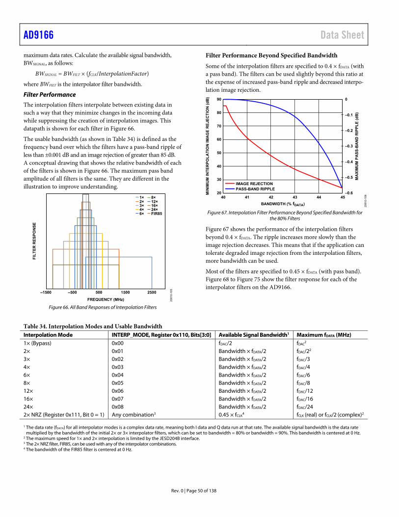
AD9166 Data Sheet
Rev. 0 | Page 50 of 138
maximum data rates. Calculate the available signal bandwidth, BWSIGNAL, as follows:
BWSIGNAL = BWFILT × (fCLK/InterpolationFactor)
where BWFILT is the interpolator filter bandwidth.
Filter Performance
The interpolation filters interpolate between existing data in such a way that they minimize changes in the incoming data while suppressing the creation of interpolation images. This datapath is shown for each filter in Figure 66.
The usable bandwidth (as shown in Table 34) is defined as the frequency band over which the filters have a pass-band ripple of less than ±0.001 dB and an image rejection of greater than 85 dB. A conceptual drawing that shows the relative bandwidth of each of the filters is shown in Figure 66. The maximum pass band amplitude of all filters is the same. They are different in the illustration to improve understanding.
FREQUENCY (MHz)
FILT
ER R
ESPO
NSE
1×2×3×4×6×
8×12×16×24×FIR85
2081
0-10
5
Figure 66. All Band Responses of Interpolation Filters
Filter Performance Beyond Specified Bandwidth
Some of the interpolation filters are specified to 0.4 × fDATA (with a pass band). The filters can be used slightly beyond this ratio at the expense of increased pass-band ripple and decreased interpo-lation image rejection.
90
20
0
–0.6
–0.5
–0.4
–0.3
–0.2
–0.1
30
40
50
60
70
80
40 41 42 43 44 45
MIN
IMUM
INTE
RPO
LATI
ON
IMAG
E RE
JECT
ION
(dB)
MAX
IMUM
PAS
S-BA
ND R
IPPL
E (d
B)
BANDWIDTH (% fDATA)
PASS-BAND RIPPLEIMAGE REJECTION
2081
0-10
6
Figure 67. Interpolation Filter Performance Beyond Specified Bandwidth for
the 80% Filters
Figure 67 shows the performance of the interpolation filters beyond 0.4 × fDATA. The ripple increases more slowly than the image rejection decreases. This means that if the application can tolerate degraded image rejection from the interpolation filters, more bandwidth can be used.
Most of the filters are specified to 0.45 × fDATA (with pass band). Figure 68 to Figure 75 show the filter response for each of the interpolator filters on the AD9166.
Table 34. Interpolation Modes and Usable Bandwidth Interpolation Mode INTERP_MODE, Register 0x110, Bits[3:0] Available Signal Bandwidth1 Maximum fDATA (MHz) 1× (Bypass) 0x00 fDAC/2 fDAC
2 2× 0x01 Bandwidth × fDATA/2 fDAC/22 3× 0x02 Bandwidth × fDATA/2 fDAC/3 4× 0x03 Bandwidth × fDATA/2 fDAC/4 6× 0x04 Bandwidth × fDATA/2 fDAC/6 8× 0x05 Bandwidth × fDATA/2 fDAC/8 12× 0x06 Bandwidth × fDATA/2 fDAC/12 16× 0x07 Bandwidth × fDATA/2 fDAC/16 24× 0x08 Bandwidth × fDATA/2 fDAC/24 2× NRZ (Register 0x111, Bit 0 = 1) Any combination3 0.45 × fCLK
4 fCLK (real) or fCLK/2 (complex)2 1 The data rate (fDATA) for all interpolator modes is a complex data rate, meaning both I data and Q data run at that rate. The available signal bandwidth is the data rate
multiplied by the bandwidth of the initial 2× or 3× interpolator filters, which can be set to bandwidth = 80% or bandwidth = 90%. This bandwidth is centered at 0 Hz. 2 The maximum speed for 1× and 2× interpolation is limited by the JESD204B interface. 3 The 2× NRZ filter, FIR85, can be used with any of the interpolator combinations. 4 The bandwidth of the FIR85 filter is centered at 0 Hz.
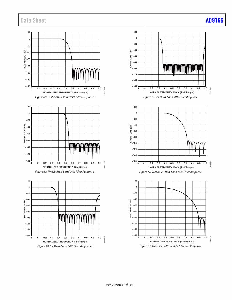
Data Sheet AD9166
Rev. 0 | Page 51 of 138
NORMALIZED FREQUENCY (Rad/Sample)
MAG
NITU
DE (d
B)
–140
–120
–100
–80
–60
–40
–20
0
20
2081
0-15
8
Figure 68. First 2× Half-Band 80% Filter Response
NORMALIZED FREQUENCY (Rad/Sample)
MAG
NITU
DE (d
B)
–140
–120
–100
–80
–60
–40
–20
0
2020
810-
159
Figure 69. First 2× Half-Band 90% Filter Response
NORMALIZED FREQUENCY (Rad/Sample)
–160
–140
–120
–100
–80
–60
–40
–20
0
20
2081
0-16
0
Figure 70. 3× Third-Band 80% Filter Response
NORMALIZED FREQUENCY (Rad/Sample)
MAG
NIT
UD
E (d
B)
–160
–140
–120
–100
–80
–60
–40
–20
0
20
2081
0-16
1
Figure 71. 3× Third-Band 90% Filter Response
NORMALIZED FREQUENCY (Rad/Sample)
MAG
NIT
UD
E (d
B)
–160
–140
–120
–100
–80
–60
–40
–20
0
20
2081
0-16
2
Figure 72. Second 2× Half-Band 45% Filter Response
NORMALIZED FREQUENCY (Rad/Sample)
0 0.1 0.2 0.3 0.4 0.5 0.6 0.7 0.8 0.9 1.0
MAG
NIT
UD
E (d
B)
–160
–140
–120
–100
–80
–60
–40
–20
0
20
2081
0-16
3
Figure 73. Third 2× Half-Band 22.5% Filter Response
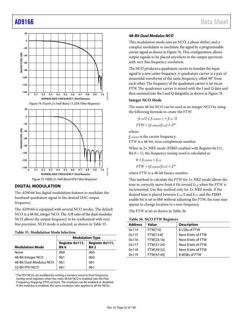
AD9166 Data Sheet
Rev. 0 | Page 52 of 138
NORMALIZED FREQUENCY (Rad/Sample)
MAG
NITU
DE (d
B)
–140
–120
–100
–80
–60
–40
–20
0
20
2081
0-16
4
Figure 74. Fourth 2× Half-Band 11.25% Filter Response
NORMALIZED FREQUENCY (Rad/Sample)
MAG
NITU
DE (d
B)
–140
–120
–100
–80
–60
–40
–20
0
2020
810-
165
Figure 75. FIR85 2× Half-Band 45% Filter Response
DIGITAL MODULATION The AD9166 has digital modulation features to modulate the baseband quadrature signal to the desired DAC output frequency.
The AD9166 is equipped with several NCO modes. The default NCO is a 48-bit, integer NCO. The A/B ratio of the dual-modulus NCO allows the output frequency to be synthesized with very fine precision. NCO mode is selected, as shown in Table 35.
Table 35. Modulation Mode Selection
Modulation Mode
Modulation Type Register 0x111, Bit 6
Register 0x111, Bit 2
None 0b0 0b0 48-Bit Integer NCO 0b1 0b0 48-Bit Dual-Modulus NCO 0b1 0b1 32-Bit FFH NCO1 0b1 0b1 1 The FFH NCOs are enabled by writing a nonzero word to their frequency
tuning word registers when the main 48-bit NCO is enabled (see the Fast Frequency Hopping (FFH) section). The modulus can be enabled or disabled. If the modulus is enabled, the same modulus ratio applies to all the NCOs.
48-Bit Dual Modulus NCO
This modulation mode uses an NCO, a phase shifter, and a complex modulator to modulate the signal by a programmable carrier signal as shown in Figure 76. This configuration allows output signals to be placed anywhere in the output spectrum with very fine frequency resolution.
The NCO produces a quadrature carrier to translate the input signal to a new center frequency. A quadrature carrier is a pair of sinusoidal waveforms of the same frequency, offset 90° from each other. The frequency of the quadrature carrier is set via an FTW. The quadrature carrier is mixed with the I and Q data and then summed into the I and Q datapaths, as shown in Figure 76.
Integer NCO Mode
The main 48-bit NCO can be used as an integer NCO by using the following formula to create the FTW:
−fCLK/2 ≤ fCARRIER < + fCLK /2
FTW = (fCARRIER/fCLK) × 248
where: fCARRIER is the carrier frequency. FTW is a 48-bit, twos complement number.
When in 2× NRZ mode (FIR85 enabled with Register 0x111, Bit 0 = 1), the frequency tuning word is calculated as
0 ≤ fCARRIER < fCLK
FTW = (fCARRIER/fCLK) × 248
where FTW is a 48-bit binary number.
This method to calculate the FTW for 2× NRZ mode allows the tone to correctly move from 0 Hz toward fCLK when the FTW is incremented. Use this method only for 2× NRZ mode. If the desired tone is placed between fCLK/2 and fCLK and the FIR85 enable bit is set to 0b0 without adjusting the FTW, the tone may appear to change location to a new frequency.
The FTW is set as shown in Table 36.
Table 36. NCO FTW Registers Address Value Description 0x114 FTW[7:0] 8 LSBs of FTW 0x115 FTW[15:8] Next 8 bits of FTW 0x116 FTW[23:16] Next 8 bits of FTW 0x117 FTW[31:24] Next 8 bits of FTW 0x118 FTW[39:32] Next 8 bits of FTW 0x119 FTW[47:40] 8 MSBs of FTW
Data Sheet AD9166
Rev. 0 | Page 53 of 138
Unlike other registers, the FTW registers are not updated immediately upon writing. Instead, the FTW registers update on the rising edge of FTW_LOAD_REQ (Register 0x113, Bit 0). After an update request, FTW_LOAD_ACK (Register 0x113, Bit 1) must be high to acknowledge that the frequency tuning word has updated.
The SEL_SIDEBAND bit (Register 0x111, Bit 1 = 0b1) is a conven-ience bit that can be set to use the lower sideband modulation result, which is equivalent to flipping the sign of the frequency tuning word.
INTERPOLATION
INTERPOLATION
NCO
10
–1
COS(ωn + θ)
θ
ωπ
SIN(ωn + θ)
I DATA
Q DATA
FTW[47:0]
SEL_SIDEBAND
OUT_I
OUT_Q+
–
NCO_PHASE_OFFSET[15:0]
2081
0-10
8
Figure 76. NCO Modulator Block Diagram
Modulus NCO Mode (Direct Digital Synthesis (DDS))
The main 48-bit NCO can also be used in a dual-modulus mode to create fractional frequencies beyond the 48-bit accuracy. The modulus mode is enabled by programming the MODULUS_EN bit in the DATAPATH_CFG register to 1 (Register 0x111, Bit 2 = 0b1).
The frequency ratio for the programmable modulus DDS is very similar to that of the typical accumulator-based DDS. The only difference is that N is not required to be a power of two for the programmable modulus, but can be an arbitrary integer. In practice, hardware constraints place limits on the range of values for N. As a result, the modulus extends the use of the NCO to applications that require exact rational frequency synthesis. The underlying function of the programmable modulus technique is to alter the accumulator modulus.
Implementation of the programmable modulus function within the AD9166 is such that the fraction, M/N, is expressible using the following equation. Note that the form of the equation implies a compound FTW with X representing the integer part and A/B representing the fractional part.
482BAX
NM
ff
DAC
CARRIER
where: X is programmed in Register 0x114 to Register 0x119. A is programmed in Register 0x12A to Register 0x12F. B is programmed in Register 0x124 to Register 0x129.
Programmable Modulus Example
Consider the case in which fCLK = 2500 MHz and the desired value of fCARRIER is 250 MHz. This scenario synthesizes an output frequency that is not a power of two submultiple of the sample rate, namely fCARRIER = (1/10) fCLK, which is not possible with a typical accumulator-based DDS.
The frequency ratio, fCARRIER/fCLK, leads directly to M and N, which are determined by reducing the fraction (250,000,000/2,500,000,000) to its lowest terms, that is,
M/N = 250,000,000/2,500,000,000 = 1/10
Therefore, M = 1 and N = 10.
After calculation, X = 28,147,497,671,065, A = 3, and B = 5. Programming these values into the registers for X, A, and B (X is programmed in Register 0x114 to Register 0x119, B is programmed in Register 0x124 to Register 0x129, and A is programmed in Register 0x12A to Register 0x12F) causes the NCO to produce an output frequency of exactly 250 MHz given a 2500 MHz sampling clock. For more details, refer to the AN-953 Application Note on the Analog Devices, Inc., website.
NCO Reset
Resetting the NCO can be useful when determining the start time and phase of the NCO. The NCO can be reset by several differ-ent methods, including a SPI write, using the TX_ENABLE pin, or by the SYSREF± signal. Due to internal timing variations from device to device, these methods achieve an accuracy of ±6 fCLK cycles.
Program Register 0x800, Bits[7:6] to 0b01 to set the NCO in phase discontinuous switching mode via a write to the SPI port. Then, any time the frequency tuning word is updated, the NCO phase accumulator resets and the NCO begins counting at the new frequency tuning word.
Fast Frequency Hopping (FFH)
To support fast frequency hopping, the AD9166 has several features in the NCO block. There are two implementations of the NCO function. The main 48-bit NCO is a general-purpose NCO and supports some of the fast frequency hopping modes, whereas the fast frequency hopping NCO is specifically designed to support several different fast frequency hopping modes.
Main NCO Frequency Hopping
In the main 48-bit NCO, the mode of updating the frequency tuning word can be changed from requiring a write to the FTW_LOAD_REQ bit (Register 0x113, Bit 0) to an automatic update mode. In the automatic update mode, the frequency tuning word is updated as soon as the chosen frequency tuning word is written.
To set the automatic frequency tuning word update mode, write the appropriate word to the FTW_REQ_MODE bits (Register 0x113, Bits[6:4]), choosing the particular frequency tuning word that causes the automatic update.
AD9166 Data Sheet
Rev. 0 | Page 54 of 138
For example, if relatively coarse frequency steps are needed, it may be sufficient to write a single word to the MSB byte of the frequency tuning word, and therefore the FTW_REQ_MODE bits can be programmed to 110 (Register 0x113, Bits[6:4] = 0b110). Then, each time the most significant byte, FTW5, is written, the NCO frequency tuning word is automatically updated.
The FTW_REQ_MODE bits can be configured to use any frequency tuning word as the automatic update trigger word. This configuration provides convenience when choosing the order in which to program the FTW registers.
The speed of the SPI port write function is a minimum of 100 MHz (see Table 9). Thus, the NCO frequency tuning word can be updated in as little as 240 ns with a one-register write in automatic update mode.
FFH NCO
The fast frequency hopping NCO is implemented as the main 48-bit NCO with an additional 31, 32-bit NCOs, with an associated bank of 31 frequency tuning words. These frequency tuning words can be preloaded into the hopping frequency register bank. Any of the 32 frequency tuning words can be selected by a one-register write to the HOPF_SEL bits in the HOPF_CTRL register (Register 0x800, Bits[4:0]). The manner in which the NCO transitions to the new frequency is determined by the hopping frequency change mode selection.
The fast frequency hopping NCO supports several modes for transitioning the phase of the NCO output as the output is hopped to a new frequency: phase continuous switching, phase discontinuous switching, and phase coherent switching. The NCO frequency change modes are listed in Table 37.
Table 37. NCO Frequency Change Mode Register 0x800, Bits[7:6] Description 0b00 Phase continuous switch 0b01 Phase discontinuous switch (reset
NCO accumulator) 0b10 Phase coherent switch
In phase continuous switching, the frequency tuning word of the NCO is updated and the phase accumulator continues to accumulate to the new frequency.
In phase discontinuous mode, the frequency tuning word of the NCO is updated and the phase accumulator is reset, making an instantaneous jump to the new frequency.
In phase coherent mode, the bank of additional 31 phase accumulators is enabled, one each to shadow each FTW in the hopping frequency register bank.
Upon enabling the phase coherent switching mode (Register 0x800, Bits[7:6] = 0b10), all 32 NCO phase accumulators begin counting simultaneously, and all continue counting regardless of which individual NCO output is currently being used in the digital datapath. In this way, the frequency of an individual NCO can be chosen and is always phase coherent to Time 0. Therefore, it is recommended to preload all frequency tuning
words, then select the phase coherent switch mode to start them at the same time.
To conserve power, each of the 31 additional NCOs and phase accumulators is enabled only when a frequency tuning word is programmed into its register. To power down a particular NCO and phase accumulator, program all zeros to the FTW register for a given NCO. All NCO frequency tuning words have a default value of 0x0. The main 48-bit NCO, which is FTW0 in the fast frequency hopping NCO, is enabled by the NCO_EN bit in the DATAPATH_CFG register (Register 0x111, Bit 6 = 0b1).
To ensure that there is no residual power consumption or possible residual spurious from one of the 32-bit NCOs after powering it up and then powering it down, the suggested method to power down the additional NCO is to first program the frequency tuning word to 0x0001, and then program it to 0x0000. This procedure ensures that the phase accumulator is flushed of residual values prior to receiving the all 0s word, which powers down the output but not the accumulator. The accumulator is powered down with the NCO_EN bit in Register 0x111, Bit 6.
NCO Only Mode
The AD9166 is capable of operating in a mode with only the modulus NCO enabled, to function as a DDS, without a JESD204B link. In this mode, a single-tone sine wave is generated by the NCO, mixed with dc data samples to set the tone amplitude, and sent to the DAC output. Thus, NCO only mode is sometimes referred to as dc test mode. The dc data samples are generated internally, without the need for a functional JESD204B link to provide the data samples. All of the features described in the Digital Modulation section are available in the NCO only mode. It is not necessary to bring up the JESD204B link in this mode.
NCO only mode is a useful option, for example, to generate a sine wave for setting up a transmitter radio signal chain without the need for a digital data source from a JESD204B transmitter. The NCO only mode can also be used in applications where a sine wave is all that is needed, such as in a local oscillator (LO) application, as an LO to a mixing stage.
To enable the NCO only mode, program the DC_TEST_EN bit in Register 0x150, Bit 1 = 0b1. Then, program a dc value into the twos complement dc test data word in Register 0x14E (MSB) and Register 0x14F (LSB). The default value is 0x0000 (zero amplitude), and a typical value to program is 0x7FFF for a full-scale tone. The final step is to program the interpolation value to 1× bypass mode by selecting INTERP_MODE = 0b0000 in Register 0x110, Bits[3:0]. This step is necessary because the dc test value is only available in the bypass path and is not accessible in the complex datapath.
When DC_TEST_EN = 1, the data source of the digital datapath is the dc test data word. This means that the JESD204B link can be brought up and data can be transferred to the device over the link, but the data is not presented to the DAC when DC_TEST_EN = 1. Connection to the SERDES data source is only achieved when
Data Sheet AD9166
Rev. 0 | Page 55 of 138
DC_TEST_EN = 0. The DC_TEST_EN bit can be toggled to switch the NCO input between SERDES data and dc data while the device is playing a signal (hot switching), but because switching to the SERDES datapath normally requires synchronizing a JESD204B link and/or setting the interpolation value, hot switching the DC_TEST_EN bit is not normally practical.
INVERSE SINC The AD9166 provides a digital inverse sinc filter to compensate the DAC roll-off over frequency. The filter is enabled by setting the INVSINC_EN bit (Register 0x111, Bit 7) and is disabled by default.
The inverse sinc (sinc−1) filter is a seven-tap FIR filter. Figure 77 shows the frequency response of sin(x)/x roll-off, the inverse sinc filter, and the composite response. The composite response has less than ±0.05 dB pass-band ripple up to a frequency of 0.4 × fCLK. When 2× NRZ mode is enabled, the inverse sinc filter operates to 0.4 × 2× fCLK.
To provide the necessary peaking at the upper end of the pass band without the risk of clipping, the inverse sinc filter has an intrinsic insertion loss of about 3.8 dB (shown in Figure 77).
1
0
MA
GN
ITU
DE
(dB
) –1
–2
–3
–4
–50 0.05 0.10 0.15 0.20
FREQUENCY (× fDAC)0.25 0.30 0.35 0.450.40 0.50
SIN(x)/x ROLL-OFFSINC–1 FILTER RESPONSECOMPOSITE RESPONSE
2081
0-10
9
Figure 77. Responses of Sin(x)/x Roll-Off, the Sinc−1 Filter, and the Composite
of the Two
DOWNSTREAM PROTECTION The AD9166 has several features designed to protect the power amplifier of the system, as well as other downstream blocks. These features consist of a control signal from the LMFC sync logic and a transmit enable function. The protection mechanism in each case is the blanking of data that is passed to the DAC decoder. The differences lie in the location in the datapath and slight variations of functionality.
The JESD204B serial link has several flags and quality measures to indicate the serial link is active and running error free. If any of these measures flags an issue, a signal from the LMFC sync logic is sent to a mux that stops data from flowing to the DAC decoder and replaces it with 0s.
There are several transmit enable features, including a TX_ ENABLE register that can be used to squelch data at several points in the datapath or configure the TX_ENABLE pin to do likewise.
Transmit Enable
The transmit enable feature can be configured either as a SPI controlled function or a pin controlled function, and can be used for several different purposes. The SPI controlled function has less accurate timing due to its reliance on a microcontroller to program it. Therefore, it is typically used as a preventative measure at power-up or when configuring the device.
The SPI controlled TX_ENABLE function can be used to zero the input to the digital datapath or to zero the output from the digital datapath, as shown in Figure 78. If the input to the digital datapath is zeroed, any filtering that is selected filters the 0 signal, causing a gradual ramp-down of energy in the digital datapath. If the digital datapath is bypassed, as in 1× interpolation mode, the data at the input to the DAC immediately drops to zero.
MAINDIGITAL
PATH
DATA
FROM LMFCSYNC LOGIC
0
0
FROM REG0x03F[6]
TX_ENABLE
FROM REG0x03F[1]
0
FROM REG0x03F[7]
TX_ENABLE
FROM REG0x03F[2]
TO DAC
2081
0-11
0
Figure 78. Downstream Protection Block Diagram
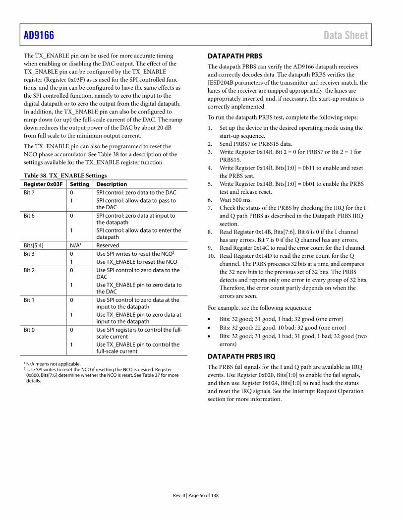
AD9166 Data Sheet
Rev. 0 | Page 56 of 138
The TX_ENABLE pin can be used for more accurate timing when enabling or disabling the DAC output. The effect of the TX_ENABLE pin can be configured by the TX_ENABLE register (Register 0x03F) as is used for the SPI controlled func-tions, and the pin can be configured to have the same effects as the SPI controlled function, namely to zero the input to the digital datapath or to zero the output from the digital datapath. In addition, the TX_ENABLE pin can also be configured to ramp down (or up) the full-scale current of the DAC. The ramp down reduces the output power of the DAC by about 20 dB from full scale to the minimum output current.
The TX_ENABLE pin can also be programmed to reset the NCO phase accumulator. See Table 38 for a description of the settings available for the TX_ENABLE register function.
Table 38. TX_ENABLE Settings Register 0x03F Setting Description Bit 7 0 SPI control: zero data to the DAC 1 SPI control: allow data to pass to
the DAC Bit 6 0 SPI control: zero data at input to
the datapath 1 SPI control: allow data to enter the
datapath Bits[5:4] N/A1 Reserved Bit 3 0 Use SPI writes to reset the NCO2 1 Use TX_ENABLE to reset the NCO Bit 2 0 Use SPI control to zero data to the
DAC 1 Use TX_ENABLE pin to zero data to
the DAC Bit 1 0 Use SPI control to zero data at the
input to the datapath 1 Use TX_ENABLE pin to zero data at
input to the datapath Bit 0 0 Use SPI registers to control the full-
scale current 1 Use TX_ENABLE pin to control the
full-scale current 1 N/A means not applicable. 2. Use SPI writes to reset the NCO if resetting the NCO is desired. Register
0x800, Bits[7:6] determine whether the NCO is reset. See Table 37 for more details.
DATAPATH PRBS The datapath PRBS can verify the AD9166 datapath receives and correctly decodes data. The datapath PRBS verifies the JESD204B parameters of the transmitter and receiver match, the lanes of the receiver are mapped appropriately, the lanes are appropriately inverted, and, if necessary, the start-up routine is correctly implemented.
To run the datapath PRBS test, complete the following steps:
1. Set up the device in the desired operating mode using the start-up sequence.
2. Send PRBS7 or PRBS15 data. 3. Write Register 0x14B. Bit 2 = 0 for PRBS7 or Bit 2 = 1 for
PRBS15. 4. Write Register 0x14B, Bits[1:0] = 0b11 to enable and reset
the PRBS test. 5. Write Register 0x14B, Bits[1:0] = 0b01 to enable the PRBS
test and release reset. 6. Wait 500 ms. 7. Check the status of the PRBS by checking the IRQ for the I
and Q path PRBS as described in the Datapath PRBS IRQ section.
8. Read Register 0x14B, Bits[7:6]. Bit 6 is 0 if the I channel has any errors. Bit 7 is 0 if the Q channel has any errors.
9. Read Register 0x14C to read the error count for the I channel. 10. Read Register 0x14D to read the error count for the Q
channel. The PRBS processes 32 bits at a time, and compares the 32 new bits to the previous set of 32 bits. The PRBS detects and reports only one error in every group of 32 bits. Therefore, the error count partly depends on when the errors are seen.
For example, see the following sequences:
Bits: 32 good; 31 good, 1 bad; 32 good (one error) Bits: 32 good; 22 good, 10 bad; 32 good (one error) Bits: 32 good; 31 good, 1 bad; 31 good, 1 bad; 32 good (two
errors)
DATAPATH PRBS IRQ The PRBS fail signals for the I and Q path are available as IRQ events. Use Register 0x020, Bits[1:0] to enable the fail signals, and then use Register 0x024, Bits[1:0] to read back the status and reset the IRQ signals. See the Interrupt Request Operation section for more information.
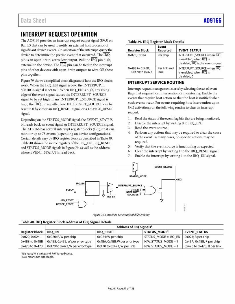
Data Sheet AD9166
Rev. 0 | Page 57 of 138
INTERRUPT REQUEST OPERATION The AD9166 provides an interrupt request output signal (IRQ) on Ball L5 that can be used to notify an external host processor of significant device events. On assertion of the interrupt, query the device to determine the precise event that occurred. The IRQ pin is an open-drain, active low output. Pull the IRQ pin high, external to the device. The IRQ pin can be tied to the interrupt pins of other devices with open-drain outputs to wire-OR these pins together.
Figure 79 shows a simplified block diagram of how the IRQ blocks work. When the IRQ_EN signal is low, the INTERRUPT_ SOURCE signal is set to 0. When IRQ_EN is high, any rising edge of the event signal causes the INTERRUPT_SOURCE signal to be set high. If any INTERRUPT_SOURCE signal is high, the IRQ pin is pulled low. INTERRUPT_SOURCE can be reset to 0 by either an IRQ_RESET signal or a DEVICE_RESET signal.
Depending on the STATUS_MODE signal, the EVENT_STATUS bit reads back an event signal or INTERRUPT_SOURCE signal. The AD9166 has several interrupt register blocks (IRQ) that can monitor up to 75 events (depending on device configuration). Certain details vary by IRQ register block as described in Table 39. Table 40 shows the source registers of the IRQ_EN, IRQ_RESET, and STATUS_MODE signals in Figure 79, as well as the address where EVENT_STATUS is read back.
Table 39. IRQ Register Block Details
Register Block Event Reported EVENT_STATUS
0x020, 0x024 Per chip INTERRUPT_SOURCE when IRQ is enabled; when IRQ is disabled, IRQ is the event signal
0x4B8 to 0x4BB; 0x470 to 0x473
Per link and lane
INTERRUPT_SOURCE when IRQ is enabled; when IRQ is disabled, 0
INTERRUPT SERVICE ROUTINE Interrupt request management starts by selecting the set of event flags that require host intervention or monitoring. Enable the events that require host action so that the host is notified when such events occur. For events requiring host intervention upon IRQ activation, run the following routine to clear an interrupt request:
1. Read the status of the event flag bits that are being monitored. 2. Disable the interrupt by writing 0 to IRQ_EN. 3. Read the event source. 4. Perform any actions that may be required to clear the cause
of the event. In many cases, no specific actions may be required.
5. Verify that the event source is functioning as expected. 6. Clear the interrupt by writing 1 to the IRQ_RESET signal. 7. Enable the interrupt by writing 1 to the IRQ_EN signal.
IRQ_EN
EVENT
DEVICE_RESET
EVENT_STATUS
INTERRUPT_SOURCE
IRQ_EN
STATUS_MODE
10
10
OTHERINTERRUPT
SOURCES
IRQ
IRQ_RESET
2081
0-11
1
Figure 79. Simplified Schematic of IRQ Circuitry
Table 40. IRQ Register Block Address of IRQ Signal Details
Register Block Address of IRQ Signals1
IRQ_EN IRQ_RESET STATUS_MODE2 EVENT_STATUS 0x020, 0x024 0x020; R/W per chip 0x024; W per chip STATUS_MODE = IRQ_EN 0x024; R per chip 0x4B8 to 0x4BB 0x4B8, 0x4B9; W per error type 0x4BA, 0x4BB; W per error type N/A, STATUS_MODE = 1 0x4BA, 0x4BB; R per chip 0x470 to 0x473 0x470 to 0x473; W per error type 0x470 to 0x473; W per link N/A, STATUS_MODE = 1 0x470 to 0x473; R per link 1 R is read; W is write; and R/W is read/write. 2 N/A means not applicable.
AD9166 Data Sheet
Rev. 0 | Page 58 of 138
APPLICATIONS INFORMATION HARDWARE CONSIDERATIONS Power Supply Recommendations
All AD9166 supply domains must remain as noise free as possible for optimal operation. Power supply noise carries frequency content that may adversely affect performance, and it may appear in the output spectrum of the device.
An inductor/capacitor (LC) filter on the output of the power supply is recommended to attenuate the noise, and must be placed as close to the AD9166 as possible.
The DAC_1P2_CLK supply is the most noise sensitive supply on the device, where phase noise and other spectral content are modulated directly onto the output signal. Other analog supplies are sensitive as well. DAC_2P5_AN and DAC_N1P2_AN are the DAC output rails and modulate noise onto the DAC output and into the amplifier input. AMP_5V_IN, AMP_3P3_OUT, and AMP_N5 are the analog rails for the amplifier input and output and may similarly modulate noise onto the output.
It is highly recommended that DAC_1P2_CLK be supplied by itself with an ultralow noise regulator such as the ADM7154 or ADP1761, with high power supply rejection ratio (PSRR) specifications to filter any unwanted switching supply noise, and achieve optimal phase noise performance.
Noisier regulators impose phase noise onto the DAC output, the amplifier input and output, and ultimately onto the output signal at the RFOUT pin.
The DAC_1P2_AN supply can be connected to the digital DAC_1P2_DIG supply with a separate filter network.
Connect DAC_1P2_SER, the 1.2V supply for the JESD204B circuitry, to a separate regulator.
The AMP_3P3 supply can be connected to the AMP_3P3_OUT RF output supply with a separate filter network.
The VDD_IO supply can be connected to either the AMP_3P3 or the AMP_3P3_OUT supply with a separate filter network. VDD_IO can also be powered separately from a system controller (for example, a microcontroller), 1.8 V to 3.3 V supply. The power supply sequencing requirement must be met, where AMP_3P3 must come up with or before VDD_IO.
Take note of the maximum power consumption numbers given in Table 2 to ensure the power supply design can tolerate tempera-ture and IC process variation extremes. The amount of current drawn is dependent on the chosen use cases. Specifications are provided for several use cases to illustrate examples and contributions from individual blocks, and to assist in calculating the maximum required current per supply.
Another consideration for the power supply design is peak current handling capability. The AD9166 draws more current in the main digital supply (DAC_1P2_DIG) when synthesizing a signal with significant amplitude variations, such as a modulated signal with high peak to average power ratio (PAPR)
or burst signals such as global system for mobile communications (GSM), time division multiple access (TDMA), or other signals that have an on and off time domain response. Therefore, the power supply must be able to supply current quickly to accommodate burst signals. Because the amount of current variation depends on the signals used, it is recommended to perform lab testing first to establish ranges. A typical variation can be several hundred milliamperes over a short time period, requiring more than 220 μF of bulk capacitance with low ESR.
Power Sequencing
The AD9166 requires power sequencing to avoid damage to internal circuitry. A board design with the AD9166 must include a power sequencer chip, such as the LTC2928, to ensure that the domains power up in the correct order. To minimize current transients during startup, separate high power, noncritical power domains across the sequence.
Perform the power-up sequence in the following order, and ensure that the supplies in each group power up and settle together:
1. DAC_1P2_DIG, AMP_3P3, AMP_3P3_OUT, VDD_IO, DAC_3P3_SYNC, AMP_N5, DAC_1P2_AN, DAC_1P2_CLK
2. DAC_N1P2_AN, DAC_1P2_SER 3. AMP_5V_IN, DAC_2P5_AN (can be derived from
AMP_5V_IN)
Within each group, monitor the supply with the longest settling time to ensure that all the supplies settle to their target voltage before sequencing to the next group.
There are no requirements for a power-down sequence.
Power and Ground Planes
Solid ground planes are recommended to avoid ground loops and to provide a solid, uninterrupted ground reference for the high speed transmission lines that require controlled impedances. For high frequency filtering, stack power planes between ground layers. Stacking also adds extra filtering and isolation between power supply domains (in addition to the decoupling capacitors).
Do not use segmented power planes as a reference for controlled impedances unless the entire length of the controlled impedance trace traverses across only a single segmented plane. These and additional guidelines for the topology of high speed transmission lines are described in the JESD204B Serial Interface Inputs (SERDIN0± to SERDIN7±) section.
For some applications, where highest performance and higher output frequencies are required, the choice of PCB materials significantly impacts results. For example, materials such as polyimide or materials from the Rogers Corporation can be used to improve tolerance to high temperatures and improve performance. Materials from Rogers such as the RO43xx series, or from Isola, such as Tachyon, are typically used for the top
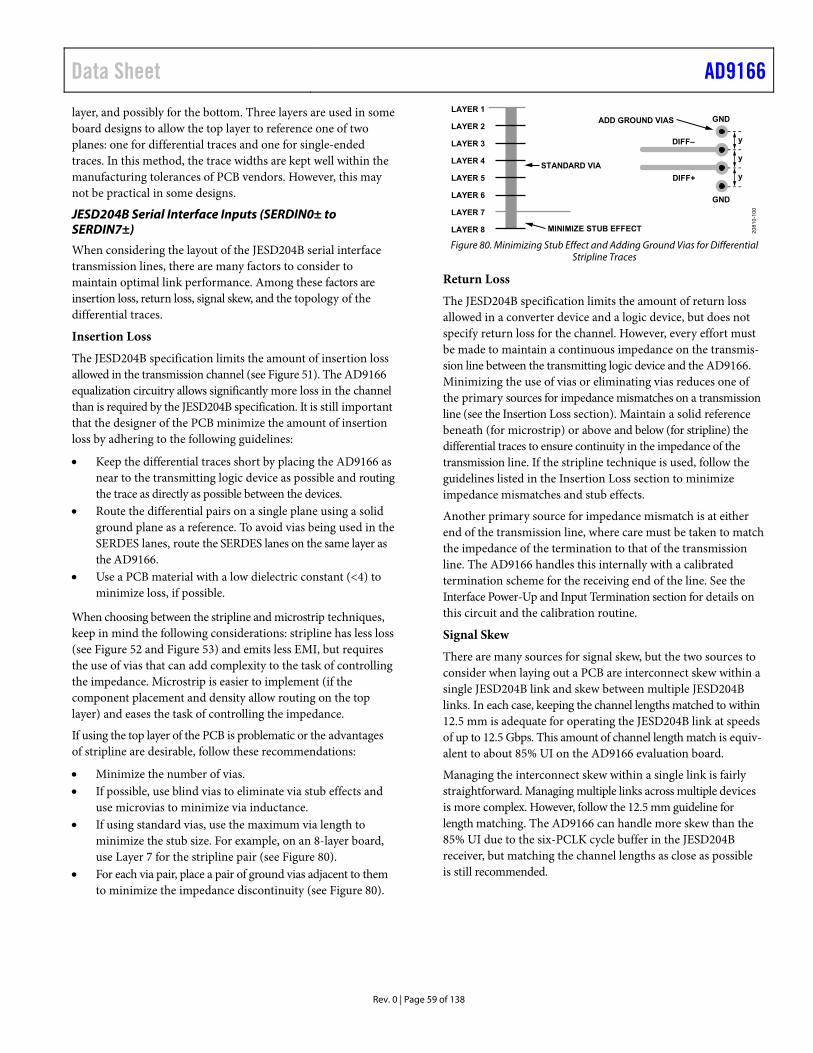
Data Sheet AD9166
Rev. 0 | Page 59 of 138
layer, and possibly for the bottom. Three layers are used in some board designs to allow the top layer to reference one of two planes: one for differential traces and one for single-ended traces. In this method, the trace widths are kept well within the manufacturing tolerances of PCB vendors. However, this may not be practical in some designs.
JESD204B Serial Interface Inputs (SERDIN0± to SERDIN7±)
When considering the layout of the JESD204B serial interface transmission lines, there are many factors to consider to maintain optimal link performance. Among these factors are insertion loss, return loss, signal skew, and the topology of the differential traces.
Insertion Loss
The JESD204B specification limits the amount of insertion loss allowed in the transmission channel (see Figure 51). The AD9166 equalization circuitry allows significantly more loss in the channel than is required by the JESD204B specification. It is still important that the designer of the PCB minimize the amount of insertion loss by adhering to the following guidelines:
Keep the differential traces short by placing the AD9166 as near to the transmitting logic device as possible and routing the trace as directly as possible between the devices.
Route the differential pairs on a single plane using a solid ground plane as a reference. To avoid vias being used in the SERDES lanes, route the SERDES lanes on the same layer as the AD9166.
Use a PCB material with a low dielectric constant (<4) to minimize loss, if possible.
When choosing between the stripline and microstrip techniques, keep in mind the following considerations: stripline has less loss (see Figure 52 and Figure 53) and emits less EMI, but requires the use of vias that can add complexity to the task of controlling the impedance. Microstrip is easier to implement (if the component placement and density allow routing on the top layer) and eases the task of controlling the impedance.
If using the top layer of the PCB is problematic or the advantages of stripline are desirable, follow these recommendations:
Minimize the number of vias. If possible, use blind vias to eliminate via stub effects and
use microvias to minimize via inductance. If using standard vias, use the maximum via length to
minimize the stub size. For example, on an 8-layer board, use Layer 7 for the stripline pair (see Figure 80).
For each via pair, place a pair of ground vias adjacent to them to minimize the impedance discontinuity (see Figure 80).
LAYER 1
LAYER 2
LAYER 3
LAYER 4
LAYER 5
LAYER 6
LAYER 7
LAYER 8 MINIMIZE STUB EFFECT
GND
GND
DIFF–
DIFF+
y
y
y
ADD GROUND VIAS
STANDARD VIA
2081
0-10
0
Figure 80. Minimizing Stub Effect and Adding Ground Vias for Differential
Stripline Traces
Return Loss
The JESD204B specification limits the amount of return loss allowed in a converter device and a logic device, but does not specify return loss for the channel. However, every effort must be made to maintain a continuous impedance on the transmis-sion line between the transmitting logic device and the AD9166. Minimizing the use of vias or eliminating vias reduces one of the primary sources for impedance mismatches on a transmission line (see the Insertion Loss section). Maintain a solid reference beneath (for microstrip) or above and below (for stripline) the differential traces to ensure continuity in the impedance of the transmission line. If the stripline technique is used, follow the guidelines listed in the Insertion Loss section to minimize impedance mismatches and stub effects.
Another primary source for impedance mismatch is at either end of the transmission line, where care must be taken to match the impedance of the termination to that of the transmission line. The AD9166 handles this internally with a calibrated termination scheme for the receiving end of the line. See the Interface Power-Up and Input Termination section for details on this circuit and the calibration routine.
Signal Skew
There are many sources for signal skew, but the two sources to consider when laying out a PCB are interconnect skew within a single JESD204B link and skew between multiple JESD204B links. In each case, keeping the channel lengths matched to within 12.5 mm is adequate for operating the JESD204B link at speeds of up to 12.5 Gbps. This amount of channel length match is equiv-alent to about 85% UI on the AD9166 evaluation board.
Managing the interconnect skew within a single link is fairly straightforward. Managing multiple links across multiple devices is more complex. However, follow the 12.5 mm guideline for length matching. The AD9166 can handle more skew than the 85% UI due to the six-PCLK cycle buffer in the JESD204B receiver, but matching the channel lengths as close as possible is still recommended.
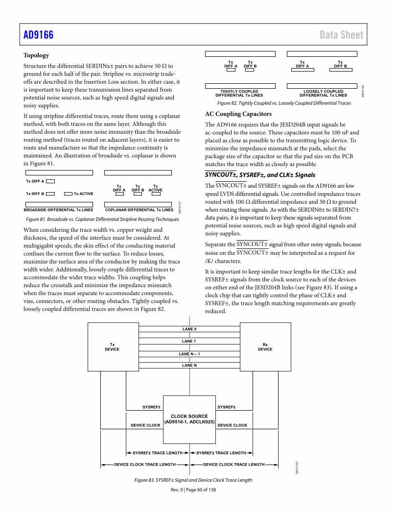
AD9166 Data Sheet
Rev. 0 | Page 60 of 138
Topology
Structure the differential SERDINx± pairs to achieve 50 Ω to ground for each half of the pair. Stripline vs. microstrip trade-offs are described in the Insertion Loss section. In either case, it is important to keep these transmission lines separated from potential noise sources, such as high speed digital signals and noisy supplies.
If using stripline differential traces, route them using a coplanar method, with both traces on the same layer. Although this method does not offer more noise immunity than the broadside routing method (traces routed on adjacent layers), it is easier to route and manufacture so that the impedance continuity is maintained. An illustration of broadside vs. coplanar is shown in Figure 81.
Tx DIFF ATx
DIFF ATx
DIFF BTx
ACTIVETx DIFF B Tx ACTIVE
BROADSIDE DIFFERENTIAL Tx LINES COPLANAR DIFFERENTIAL Tx LINES
2081
0-10
1
Figure 81. Broadside vs. Coplanar Differential Stripline Routing Techniques
When considering the trace width vs. copper weight and thickness, the speed of the interface must be considered. At multigigabit speeds, the skin effect of the conducting material confines the current flow to the surface. To reduce losses, maximize the surface area of the conductor by making the trace width wider. Additionally, loosely couple differential traces to accommodate the wider trace widths. This coupling helps reduce the crosstalk and minimize the impedance mismatch when the traces must separate to accommodate components, vias, connectors, or other routing obstacles. Tightly coupled vs. loosely coupled differential traces are shown in Figure 82.
TxDIFF A
TxDIFF A
TxDIFF B
TxDIFF B
TIGHTLY COUPLEDDIFFERENTIAL Tx LINES
LOOSELY COUPLEDDIFFERENTIAL Tx LINES 20
810-
102
Figure 82. Tightly Coupled vs. Loosely Coupled Differential Traces
AC Coupling Capacitors
The AD9166 requires that the JESD204B input signals be ac-coupled to the source. These capacitors must be 100 nF and placed as close as possible to the transmitting logic device. To minimize the impedance mismatch at the pads, select the package size of the capacitor so that the pad size on the PCB matches the trace width as closely as possible.
SYNCOUT±, SYSREF±, and CLK± Signals
The SYNCOUT± and SYSREF± signals on the AD9166 are low speed LVDS differential signals. Use controlled impedance traces routed with 100 Ω differential impedance and 50 Ω to ground when routing these signals. As with the SERDIN0± to SERDIN7± data pairs, it is important to keep these signals separated from potential noise sources, such as high speed digital signals and noisy supplies.
Separate the SYNCOUT± signal from other noisy signals, because noise on the SYNCOUT± may be interpreted as a request for /K/ characters.
It is important to keep similar trace lengths for the CLK± and SYSREF± signals from the clock source to each of the devices on either end of the JESD204B links (see Figure 83). If using a clock chip that can tightly control the phase of CLK± and SYSREF±, the trace length matching requirements are greatly reduced.
CLOCK SOURCE(AD9516-1, ADCLK925)
LANE 0
LANE 1
LANE N – 1
LANE N
DEVICE CLOCK DEVICE CLOCK
SYSREF± SYSREF±
SYSREF± TRACE LENGTH SYSREF± TRACE LENGTH
DEVICE CLOCK TRACE LENGTHDEVICE CLOCK TRACE LENGTH
TxDEVICE
RxDEVICE
2081
0-10
3
Figure 83. SYSREF± Signal and Device Clock Trace Length
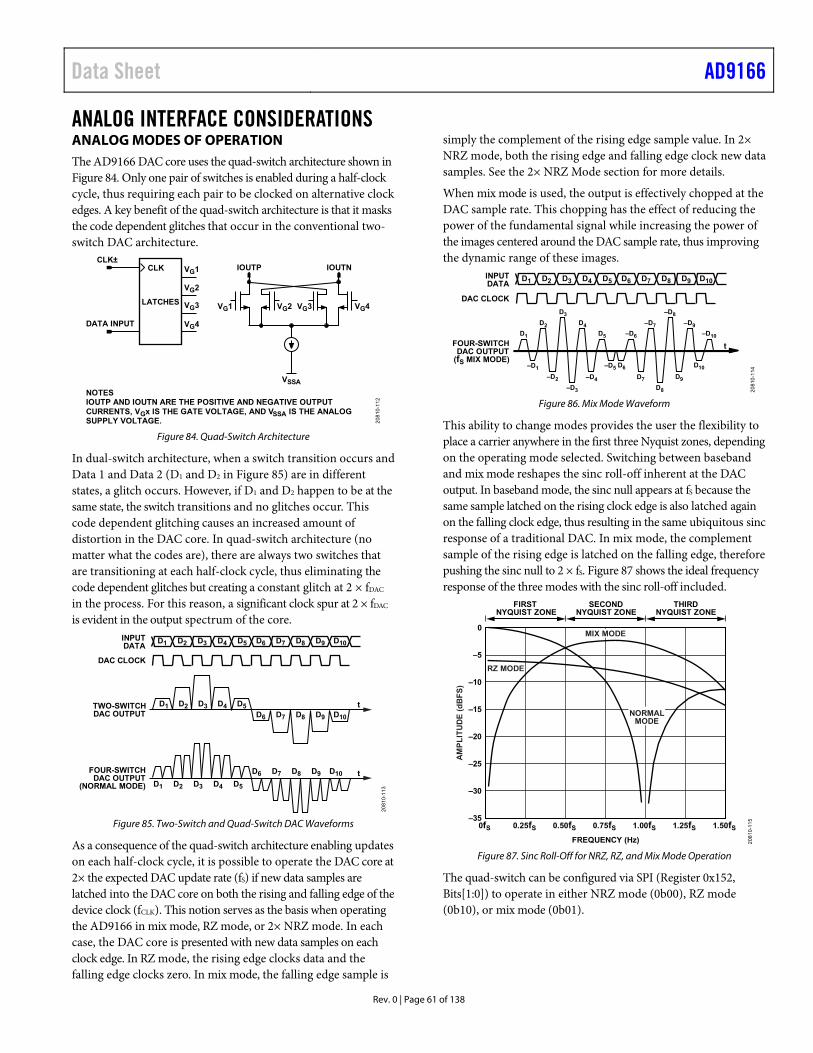
Data Sheet AD9166
Rev. 0 | Page 61 of 138
ANALOG INTERFACE CONSIDERATIONS ANALOG MODES OF OPERATION The AD9166 DAC core uses the quad-switch architecture shown in Figure 84. Only one pair of switches is enabled during a half-clock cycle, thus requiring each pair to be clocked on alternative clock edges. A key benefit of the quad-switch architecture is that it masks the code dependent glitches that occur in the conventional two-switch DAC architecture.
VG1
VSSA
IOUTP IOUTN
VG1 VG2 VG3 VG4
CLK±CLK
LATCHES
DATA INPUT
VG2
VG3
VG4
2081
0-11
2
NOTESIOUTP AND IOUTN ARE THE POSITIVE AND NEGATIVE OUTPUTCURRENTS, VGx IS THE GATE VOLTAGE, AND VSSA IS THE ANALOGSUPPLY VOLTAGE.
Figure 84. Quad-Switch Architecture
In dual-switch architecture, when a switch transition occurs and Data 1 and Data 2 (D1 and D2 in Figure 85) are in different states, a glitch occurs. However, if D1 and D2 happen to be at the same state, the switch transitions and no glitches occur. This code dependent glitching causes an increased amount of distortion in the DAC core. In quad-switch architecture (no matter what the codes are), there are always two switches that are transitioning at each half-clock cycle, thus eliminating the code dependent glitches but creating a constant glitch at 2 × fDAC in the process. For this reason, a significant clock spur at 2 × fDAC is evident in the output spectrum of the core.
INPUTDATA
DAC CLOCK
TWO-SWITCHDAC OUTPUT
FOUR-SWITCHDAC OUTPUT
(NORMAL MODE)
tD1 D2 D3 D4 D5D6 D7 D8 D9 D10
D6 D7 D8 D9 D10D1 D2 D3 D4 D5
D6 D7 D8 D9 D10D1 D2 D3 D4 D5
t
2081
0-11
3
Figure 85. Two-Switch and Quad-Switch DAC Waveforms
As a consequence of the quad-switch architecture enabling updates on each half-clock cycle, it is possible to operate the DAC core at 2× the expected DAC update rate (fS) if new data samples are latched into the DAC core on both the rising and falling edge of the device clock (fCLK). This notion serves as the basis when operating the AD9166 in mix mode, RZ mode, or 2× NRZ mode. In each case, the DAC core is presented with new data samples on each clock edge. In RZ mode, the rising edge clocks data and the falling edge clocks zero. In mix mode, the falling edge sample is
simply the complement of the rising edge sample value. In 2× NRZ mode, both the rising edge and falling edge clock new data samples. See the 2× NRZ Mode section for more details.
When mix mode is used, the output is effectively chopped at the DAC sample rate. This chopping has the effect of reducing the power of the fundamental signal while increasing the power of the images centered around the DAC sample rate, thus improving the dynamic range of these images.
INPUTDATA
DAC CLOCK
FOUR-SWITCHDAC OUTPUT
(fS MIX MODE)
–D6
–D7
–D8–D9
–D10
D6
D7D8
D9
D10–D1–D2
–D3
–D4
–D5
D1
D2
D3D4
D5
D6 D7 D8 D9 D10D1 D2 D3 D4 D5
t
2081
0-11
4
Figure 86. Mix Mode Waveform
This ability to change modes provides the user the flexibility to place a carrier anywhere in the first three Nyquist zones, depending on the operating mode selected. Switching between baseband and mix mode reshapes the sinc roll-off inherent at the DAC output. In baseband mode, the sinc null appears at fS because the same sample latched on the rising clock edge is also latched again on the falling clock edge, thus resulting in the same ubiquitous sinc response of a traditional DAC. In mix mode, the complement sample of the rising edge is latched on the falling edge, therefore pushing the sinc null to 2 × fS. Figure 87 shows the ideal frequency response of the three modes with the sinc roll-off included.
FREQUENCY (Hz)
0fS 1.50fS1.25fS1.00fS0.75fS0.50fS0.25fS–35
–30
–25
–20
–15
–10
–5
0
FIRSTNYQUIST ZONE
SECONDNYQUIST ZONE
THIRDNYQUIST ZONE
MIX MODE
RZ MODE
AMPL
ITUD
E (d
BFS)
NORMALMODE
2081
0-11
5
Figure 87. Sinc Roll-Off for NRZ, RZ, and Mix Mode Operation
The quad-switch can be configured via SPI (Register 0x152, Bits[1:0]) to operate in either NRZ mode (0b00), RZ mode (0b10), or mix mode (0b01).
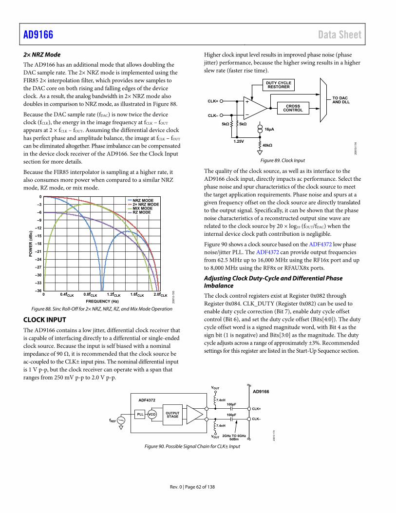
AD9166 Data Sheet
Rev. 0 | Page 62 of 138
2× NRZ Mode
The AD9166 has an additional mode that allows doubling the DAC sample rate. The 2× NRZ mode is implemented using the FIR85 2× interpolation filter, which provides new samples to the DAC core on both rising and falling edges of the device clock. As a result, the analog bandwidth in 2× NRZ mode also doubles in comparison to NRZ mode, as illustrated in Figure 88.
Because the DAC sample rate (fDAC) is now twice the device clock (fCLK), the energy in the image frequency at fCLK – fOUT appears at 2 × fCLK – fOUT. Assuming the differential device clock has perfect phase and amplitude balance, the image at fCLK – fOUT can be eliminated altogether. Phase imbalance can be compensated in the device clock receiver of the AD9166. See the Clock Input section for more details.
Because the FIR85 interpolator is sampling at a higher rate, it also consumes more power when compared to a similar NRZ mode, RZ mode, or mix mode.
–36
–33
–30
–27
–24
–21
–18
–15
–12
–9
–6
–3
0
0 0.4fCLK 0.8fCLK 1.2fCLK 1.6fCLK 2.0fCLK
POW
ER (d
Bc)
FREQUENCY (Hz)
NRZ MODE2× NRZ MODEMIX MODERZ MODE
2081
0-19
3
Figure 88. Sinc Roll-Off for 2× NRZ, NRZ, RZ, and Mix Mode Operation
CLOCK INPUT The AD9166 contains a low jitter, differential clock receiver that is capable of interfacing directly to a differential or single-ended clock source. Because the input is self biased with a nominal impedance of 90 Ω, it is recommended that the clock source be ac-coupled to the CLK± input pins. The nominal differential input is 1 V p-p, but the clock receiver can operate with a span that ranges from 250 mV p-p to 2.0 V p-p.
Higher clock input level results in improved phase noise (phase jitter) performance, because the higher swing results in a higher slew rate (faster rise time).
CLK+TO DACAND DLL
CLK–
1.25V
5kΩ 5kΩ
40kΩ
16µA
DUTY CYCLERESTORER
CROSSCONTROL
2081
0-11
6
Figure 89. Clock Input
The quality of the clock source, as well as its interface to the AD9166 clock input, directly impacts ac performance. Select the phase noise and spur characteristics of the clock source to meet the target application requirements. Phase noise and spurs at a given frequency offset on the clock source are directly translated to the output signal. Specifically, it can be shown that the phase noise characteristics of a reconstructed output sine wave are related to the clock source by 20 × log10 (fOUT/fDAC) when the internal device clock path contribution is negligible.
Figure 90 shows a clock source based on the ADF4372 low phase noise/jitter PLL. The ADF4372 can provide output frequencies from 62.5 MHz up to 16,000 MHz using the RF16x port and up to 8,000 MHz using the RF8x or RFAUX8x ports.
Adjusting Clock Duty-Cycle and Differential Phase Imbalance
The clock control registers exist at Register 0x082 through Register 0x084. CLK_DUTY (Register 0x082) can be used to enable duty cycle correction (Bit 7), enable duty cycle offset control (Bit 6), and set the duty cycle offset (Bits[4:0]). The duty cycle offset word is a signed magnitude word, with Bit 4 as the sign bit (1 is negative) and Bits[3:0] as the magnitude. The duty cycle adjusts across a range of approximately ±3%. Recommended settings for this register are listed in the Start-Up Sequence section.
VCOPLL
ADF4372
fREF
2GHz TO 6GHz0dBm
100pF7.4nH
VOUT
VOUT
7.4nH
100pF
AD9166
CLK+
CLK–OUTPUTSTAGE
2081
0-17
4
Figure 90. Possible Signal Chain for CLK± Input
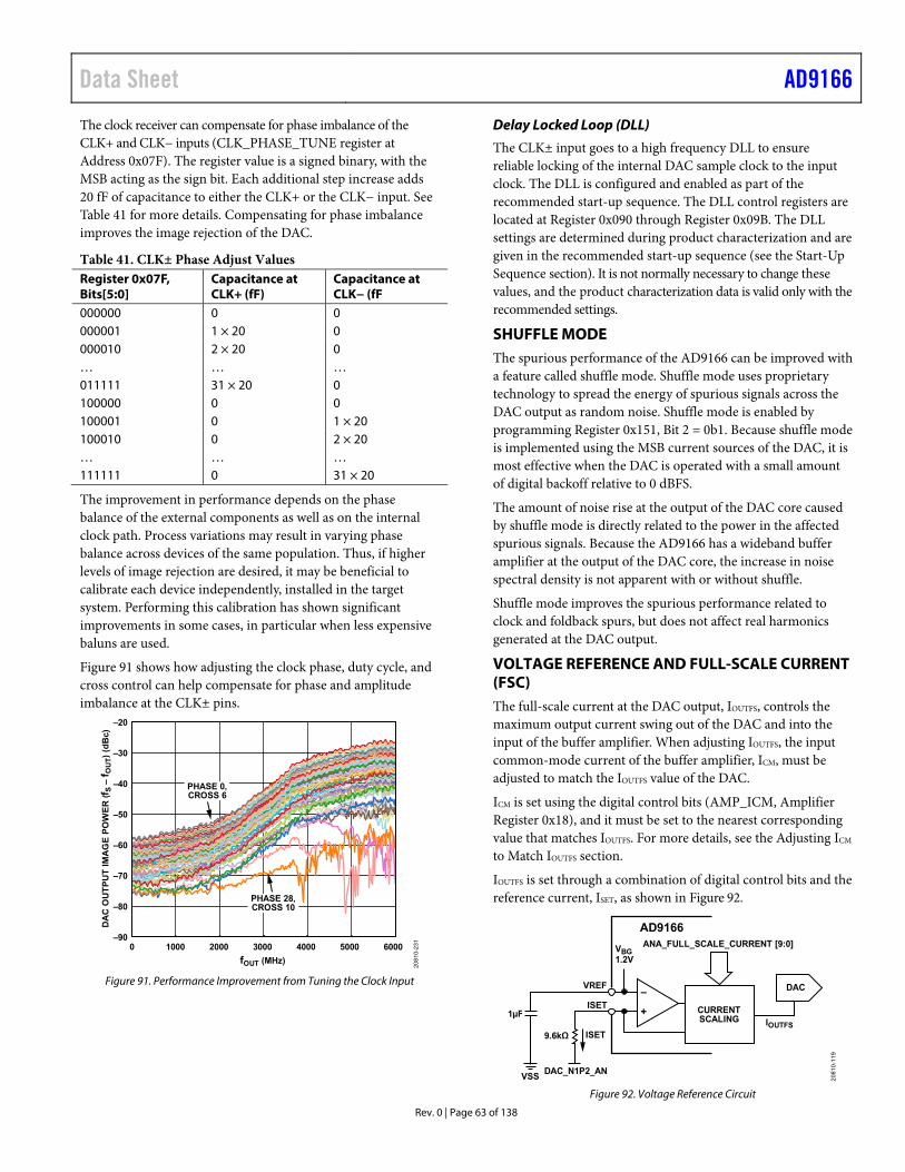
Data Sheet AD9166
Rev. 0 | Page 63 of 138
The clock receiver can compensate for phase imbalance of the CLK+ and CLK− inputs (CLK_PHASE_TUNE register at Address 0x07F). The register value is a signed binary, with the MSB acting as the sign bit. Each additional step increase adds 20 fF of capacitance to either the CLK+ or the CLK− input. See Table 41 for more details. Compensating for phase imbalance improves the image rejection of the DAC.
Table 41. CLK± Phase Adjust Values Register 0x07F, Bits[5:0]
Capacitance at CLK+ (fF)
Capacitance at CLK− (fF
000000 0 0 000001 1 × 20 0 000010 2 × 20 0 … … … 011111 31 × 20 0 100000 0 0 100001 0 1 × 20 100010 0 2 × 20 … … … 111111 0 31 × 20
The improvement in performance depends on the phase balance of the external components as well as on the internal clock path. Process variations may result in varying phase balance across devices of the same population. Thus, if higher levels of image rejection are desired, it may be beneficial to calibrate each device independently, installed in the target system. Performing this calibration has shown significant improvements in some cases, in particular when less expensive baluns are used.
Figure 91 shows how adjusting the clock phase, duty cycle, and cross control can help compensate for phase and amplitude imbalance at the CLK± pins.
PHASE 0,CROSS 6
–20
–30
–40
–50
–60
–70
–80
–900 1000 2000 3000 4000 5000 6000
PHASE 28,CROSS 10
DA
C O
UTP
UT
IMA
GE
POW
ER (f
S –
f OUT
) (dB
c)
fOUT (MHz)
2081
0-23
1
Figure 91. Performance Improvement from Tuning the Clock Input
Delay Locked Loop (DLL)
The CLK± input goes to a high frequency DLL to ensure reliable locking of the internal DAC sample clock to the input clock. The DLL is configured and enabled as part of the recommended start-up sequence. The DLL control registers are located at Register 0x090 through Register 0x09B. The DLL settings are determined during product characterization and are given in the recommended start-up sequence (see the Start-Up Sequence section). It is not normally necessary to change these values, and the product characterization data is valid only with the recommended settings.
SHUFFLE MODE The spurious performance of the AD9166 can be improved with a feature called shuffle mode. Shuffle mode uses proprietary technology to spread the energy of spurious signals across the DAC output as random noise. Shuffle mode is enabled by programming Register 0x151, Bit 2 = 0b1. Because shuffle mode is implemented using the MSB current sources of the DAC, it is most effective when the DAC is operated with a small amount of digital backoff relative to 0 dBFS.
The amount of noise rise at the output of the DAC core caused by shuffle mode is directly related to the power in the affected spurious signals. Because the AD9166 has a wideband buffer amplifier at the output of the DAC core, the increase in noise spectral density is not apparent with or without shuffle.
Shuffle mode improves the spurious performance related to clock and foldback spurs, but does not affect real harmonics generated at the DAC output.
VOLTAGE REFERENCE AND FULL-SCALE CURRENT (FSC) The full-scale current at the DAC output, IOUTFS, controls the maximum output current swing out of the DAC and into the input of the buffer amplifier. When adjusting IOUTFS, the input common-mode current of the buffer amplifier, ICM, must be adjusted to match the IOUTFS value of the DAC.
ICM is set using the digital control bits (AMP_ICM, Amplifier Register 0x18), and it must be set to the nearest corresponding value that matches IOUTFS. For more details, see the Adjusting ICM to Match IOUTFS section.
IOUTFS is set through a combination of digital control bits and the reference current, ISET, as shown in Figure 92.
CURRENTSCALING
ANA_FULL_SCALE_CURRENT [9:0]AD9166
DAC
IOUTFS9.6kΩ
1µF
VREF
ISET
VSS
ISET
VBG1.2V
+
–
DAC_N1P2_AN
2081
0-11
9
Figure 92. Voltage Reference Circuit
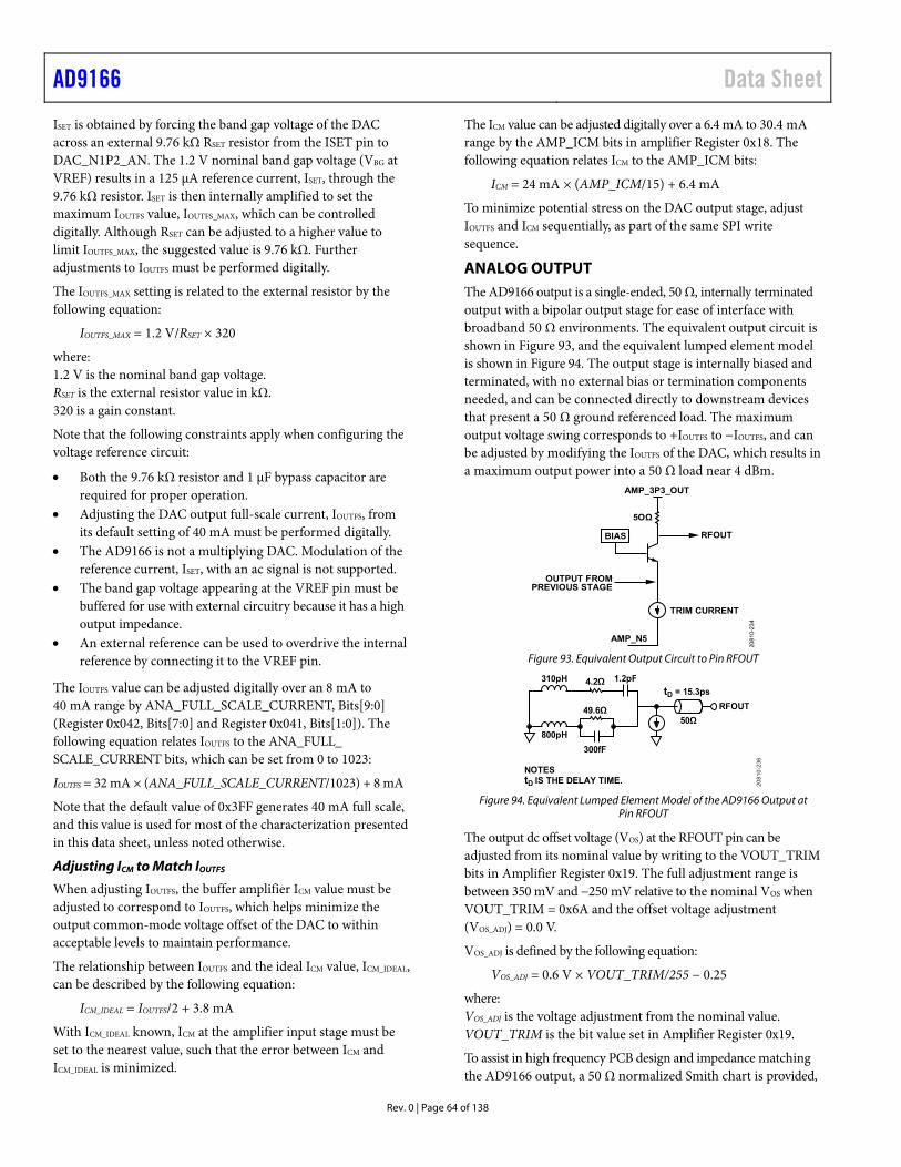
AD9166 Data Sheet
Rev. 0 | Page 64 of 138
ISET is obtained by forcing the band gap voltage of the DAC across an external 9.76 kΩ RSET resistor from the ISET pin to DAC_N1P2_AN. The 1.2 V nominal band gap voltage (VBG at VREF) results in a 125 μA reference current, ISET, through the 9.76 kΩ resistor. ISET is then internally amplified to set the maximum IOUTFS value, IOUTFS_MAX, which can be controlled digitally. Although RSET can be adjusted to a higher value to limit IOUTFS_MAX, the suggested value is 9.76 kΩ. Further adjustments to IOUTFS must be performed digitally.
The IOUTFS_MAX setting is related to the external resistor by the following equation:
IOUTFS_MAX = 1.2 V/RSET × 320
where: 1.2 V is the nominal band gap voltage. RSET is the external resistor value in kΩ. 320 is a gain constant.
Note that the following constraints apply when configuring the voltage reference circuit:
Both the 9.76 kΩ resistor and 1 μF bypass capacitor are required for proper operation.
Adjusting the DAC output full-scale current, IOUTFS, from its default setting of 40 mA must be performed digitally.
The AD9166 is not a multiplying DAC. Modulation of the reference current, ISET, with an ac signal is not supported.
The band gap voltage appearing at the VREF pin must be buffered for use with external circuitry because it has a high output impedance.
An external reference can be used to overdrive the internal reference by connecting it to the VREF pin.
The IOUTFS value can be adjusted digitally over an 8 mA to 40 mA range by ANA_FULL_SCALE_CURRENT, Bits[9:0] (Register 0x042, Bits[7:0] and Register 0x041, Bits[1:0]). The following equation relates IOUTFS to the ANA_FULL_ SCALE_CURRENT bits, which can be set from 0 to 1023:
IOUTFS = 32 mA × (ANA_FULL_SCALE_CURRENT/1023) + 8 mA
Note that the default value of 0x3FF generates 40 mA full scale, and this value is used for most of the characterization presented in this data sheet, unless noted otherwise.
Adjusting ICM to Match IOUTFS
When adjusting IOUTFS, the buffer amplifier ICM value must be adjusted to correspond to IOUTFS, which helps minimize the output common-mode voltage offset of the DAC to within acceptable levels to maintain performance.
The relationship between IOUTFS and the ideal ICM value, ICM_IDEAL, can be described by the following equation:
ICM_IDEAL = IOUTFS/2 + 3.8 mA
With ICM_IDEAL known, ICM at the amplifier input stage must be set to the nearest value, such that the error between ICM and ICM_IDEAL is minimized.
The ICM value can be adjusted digitally over a 6.4 mA to 30.4 mA range by the AMP_ICM bits in amplifier Register 0x18. The following equation relates ICM to the AMP_ICM bits:
ICM = 24 mA × (AMP_ICM/15) + 6.4 mA
To minimize potential stress on the DAC output stage, adjust IOUTFS and ICM sequentially, as part of the same SPI write sequence.
ANALOG OUTPUT The AD9166 output is a single-ended, 50 Ω, internally terminated output with a bipolar output stage for ease of interface with broadband 50 Ω environments. The equivalent output circuit is shown in Figure 93, and the equivalent lumped element model is shown in Figure 94. The output stage is internally biased and terminated, with no external bias or termination components needed, and can be connected directly to downstream devices that present a 50 Ω ground referenced load. The maximum output voltage swing corresponds to +IOUTFS to −IOUTFS, and can be adjusted by modifying the IOUTFS of the DAC, which results in a maximum output power into a 50 Ω load near 4 dBm.
TRIM CURRENT
OUTPUT FROMPREVIOUS STAGE
RFOUT
5OΩ
AMP_3P3_OUT
BIAS
AMP_N5
2081
0-23
4
Figure 93. Equivalent Output Circuit to Pin RFOUT
tD = 15.3ps
50Ω
310pH
800pH
4.2Ω
49.6Ω
300fF
1.2pF
RFOUT
2081
0-23
6
NOTEStD IS THE DELAY TIME.
Figure 94. Equivalent Lumped Element Model of the AD9166 Output at Pin RFOUT
The output dc offset voltage (VOS) at the RFOUT pin can be adjusted from its nominal value by writing to the VOUT_TRIM bits in Amplifier Register 0x19. The full adjustment range is between 350 mV and −250 mV relative to the nominal VOS when VOUT_TRIM = 0x6A and the offset voltage adjustment (VOS_ADJ) = 0.0 V.
VOS_ADJ is defined by the following equation:
VOS_ADJ = 0.6 V × VOUT_TRIM/255 − 0.25
where: VOS_ADJ is the voltage adjustment from the nominal value. VOUT_TRIM is the bit value set in Amplifier Register 0x19.
To assist in high frequency PCB design and impedance matching the AD9166 output, a 50 Ω normalized Smith chart is provided,
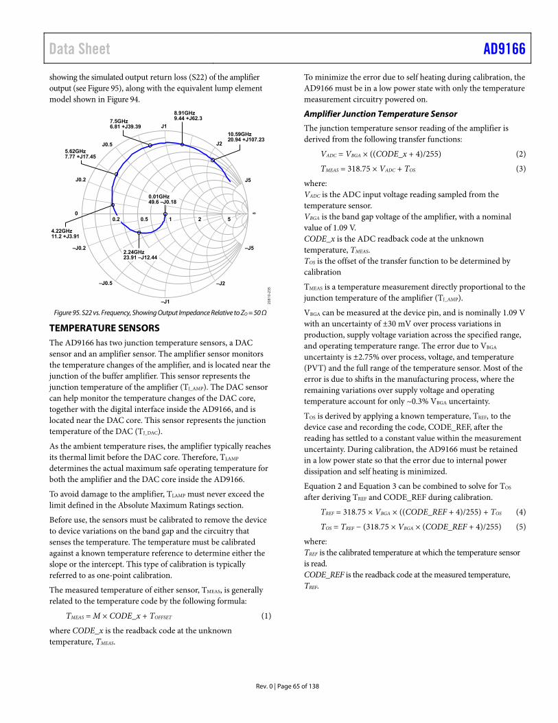
Data Sheet AD9166
Rev. 0 | Page 65 of 138
showing the simulated output return loss (S22) of the amplifier output (see Figure 95), along with the equivalent lump element model shown in Figure 94.
∞0
J5
–J5
J2
J1
–J1
–J2
J0.5
–J0.5
J0.2
–J0.2
8.91GHz9.44 +J62.37.5GHz
6.81 +J39.3910.59GHz20.94 +J107.23
0.01GHz49.6 –J0.18
2.24GHz23.91 –J12.44
5210.50.2
2081
0-23
5
5.62GHz7.77 +J17.45
4.22GHz11.2 +J3.91
Figure 95. S22 vs. Frequency, Showing Output Impedance Relative to ZO = 50 Ω
TEMPERATURE SENSORS The AD9166 has two junction temperature sensors, a DAC sensor and an amplifier sensor. The amplifier sensor monitors the temperature changes of the amplifier, and is located near the junction of the buffer amplifier. This sensor represents the junction temperature of the amplifier (TJ_AMP). The DAC sensor can help monitor the temperature changes of the DAC core, together with the digital interface inside the AD9166, and is located near the DAC core. This sensor represents the junction temperature of the DAC (TJ_DAC).
As the ambient temperature rises, the amplifier typically reaches its thermal limit before the DAC core. Therefore, TJ,AMP determines the actual maximum safe operating temperature for both the amplifier and the DAC core inside the AD9166.
To avoid damage to the amplifier, TJ,AMP must never exceed the limit defined in the Absolute Maximum Ratings section.
Before use, the sensors must be calibrated to remove the device to device variations on the band gap and the circuitry that senses the temperature. The temperature must be calibrated against a known temperature reference to determine either the slope or the intercept. This type of calibration is typically referred to as one-point calibration.
The measured temperature of either sensor, TMEAS, is generally related to the temperature code by the following formula:
TMEAS = M × CODE_x + TOFFSET (1)
where CODE_x is the readback code at the unknown temperature, TMEAS.
To minimize the error due to self heating during calibration, the AD9166 must be in a low power state with only the temperature measurement circuitry powered on.
Amplifier Junction Temperature Sensor
The junction temperature sensor reading of the amplifier is derived from the following transfer functions:
VADC = VBGA × ((CODE_x + 4)/255) (2)
TMEAS = 318.75 × VADC + TOS (3)
where: VADC is the ADC input voltage reading sampled from the temperature sensor. VBGA is the band gap voltage of the amplifier, with a nominal value of 1.09 V. CODE_x is the ADC readback code at the unknown temperature, TMEAS. TOS is the offset of the transfer function to be determined by calibration
TMEAS is a temperature measurement directly proportional to the junction temperature of the amplifier (TJ_AMP).
VBGA can be measured at the device pin, and is nominally 1.09 V with an uncertainty of ±30 mV over process variations in production, supply voltage variation across the specified range, and operating temperature range. The error due to VBGA uncertainty is ±2.75% over process, voltage, and temperature (PVT) and the full range of the temperature sensor. Most of the error is due to shifts in the manufacturing process, where the remaining variations over supply voltage and operating temperature account for only ~0.3% VBGA uncertainty.
TOS is derived by applying a known temperature, TREF, to the device case and recording the code, CODE_REF, after the reading has settled to a constant value within the measurement uncertainty. During calibration, the AD9166 must be retained in a low power state so that the error due to internal power dissipation and self heating is minimized.
Equation 2 and Equation 3 can be combined to solve for TOS after deriving TREF and CODE_REF during calibration.
TREF = 318.75 × VBGA × ((CODE_REF + 4)/255) + TOS (4)
TOS = TREF − (318.75 × VBGA × (CODE_REF + 4)/255) (5)
where: TREF is the calibrated temperature at which the temperature sensor is read. CODE_REF is the readback code at the measured temperature, TREF.
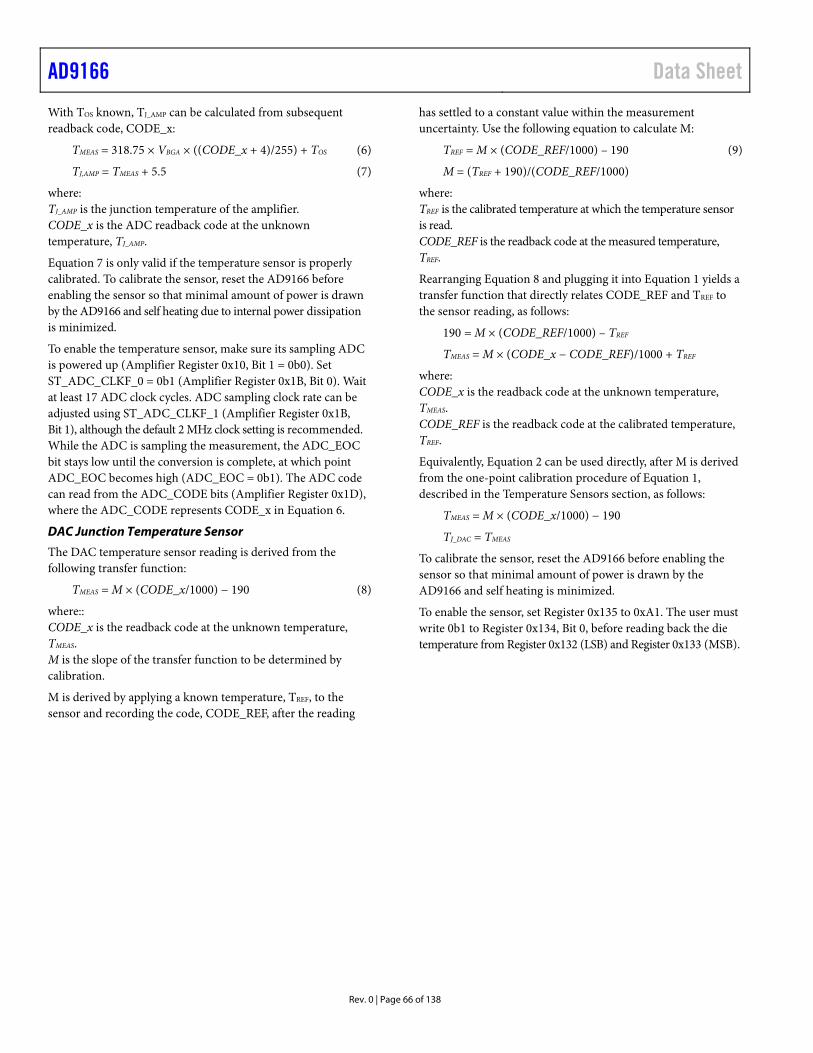
AD9166 Data Sheet
Rev. 0 | Page 66 of 138
With TOS known, TJ_AMP can be calculated from subsequent readback code, CODE_x:
TMEAS = 318.75 × VBGA × ((CODE_x + 4)/255) + TOS (6)
TJ,AMP = TMEAS + 5.5 (7)
where: TJ_AMP is the junction temperature of the amplifier. CODE_x is the ADC readback code at the unknown temperature, TJ_AMP.
Equation 7 is only valid if the temperature sensor is properly calibrated. To calibrate the sensor, reset the AD9166 before enabling the sensor so that minimal amount of power is drawn by the AD9166 and self heating due to internal power dissipation is minimized.
To enable the temperature sensor, make sure its sampling ADC is powered up (Amplifier Register 0x10, Bit 1 = 0b0). Set ST_ADC_CLKF_0 = 0b1 (Amplifier Register 0x1B, Bit 0). Wait at least 17 ADC clock cycles. ADC sampling clock rate can be adjusted using ST_ADC_CLKF_1 (Amplifier Register 0x1B, Bit 1), although the default 2 MHz clock setting is recommended. While the ADC is sampling the measurement, the ADC_EOC bit stays low until the conversion is complete, at which point ADC_EOC becomes high (ADC_EOC = 0b1). The ADC code can read from the ADC_CODE bits (Amplifier Register 0x1D), where the ADC_CODE represents CODE_x in Equation 6.
DAC Junction Temperature Sensor
The DAC temperature sensor reading is derived from the following transfer function:
TMEAS = M × (CODE_x/1000) − 190 (8)
where:: CODE_x is the readback code at the unknown temperature, TMEAS. M is the slope of the transfer function to be determined by calibration.
M is derived by applying a known temperature, TREF, to the sensor and recording the code, CODE_REF, after the reading
has settled to a constant value within the measurement uncertainty. Use the following equation to calculate M:
TREF = M × (CODE_REF/1000) – 190 (9)
M = (TREF + 190)/(CODE_REF/1000)
where: TREF is the calibrated temperature at which the temperature sensor is read. CODE_REF is the readback code at the measured temperature, TREF.
Rearranging Equation 8 and plugging it into Equation 1 yields a transfer function that directly relates CODE_REF and TREF to the sensor reading, as follows:
190 = M × (CODE_REF/1000) – TREF
TMEAS = M × (CODE_x − CODE_REF)/1000 + TREF
where: CODE_x is the readback code at the unknown temperature, TMEAS. CODE_REF is the readback code at the calibrated temperature, TREF.
Equivalently, Equation 2 can be used directly, after M is derived from the one-point calibration procedure of Equation 1, described in the Temperature Sensors section, as follows:
TMEAS = M × (CODE_x/1000) − 190
TJ_DAC = TMEAS
To calibrate the sensor, reset the AD9166 before enabling the sensor so that minimal amount of power is drawn by the AD9166 and self heating is minimized.
To enable the sensor, set Register 0x135 to 0xA1. The user must write 0b1 to Register 0x134, Bit 0, before reading back the die temperature from Register 0x132 (LSB) and Register 0x133 (MSB).
Data Sheet AD9166
Rev. 0 | Page 67 of 138
START-UP SEQUENCE Several steps are required to program the AD9166 to the proper operating state after the device is powered up according to the recommended power-up sequence (see the Power Sequencing section).
The start-up sequence is divided into several steps, and is listed in Table 42, Table 43, and Table 44, along with an explanation of the purpose of each step. Private registers are reserved but must be written for proper operation. Blank cells in Table 42 to Table 44 mean that the value depends on the result as described in the Description column.
The AD9166 is calibrated at the factory as part of the automatic test program. The configure DAC start-up sequence loads the factory calibration coefficients and configures some parameters
that optimize the performance of the DAC and the device clock DLL (see Table 42). Run this sequence whenever the DAC is powered down or reset.
The configure JESD204B sequence configures the SERDES block and then brings up the links (see Table 43). First, run the configure DAC start-up sequence, then run the configure JESD204B sequence.
Follow the configure NCO sequence if using the NCO (see Table 44). Note that the NCO can be used in NCO only mode or in conjunction with synthesized data from the SERDES data interface. Only one mode can be used at a time and this mode is selected in the second step in Table 44. The configure DAC start-up sequence is run first, then the configure NCO sequence.
Table 42. Configure DAC Start-Up Sequence After Power-Up Register Value Description R/W 0x000 0x18 Configure the device for 4-wire serial port operation (optional: leave at the default of 3-wire SPI). W 0x0D2 0x52 Reset internal calibration registers (private). W 0x0D2 0xD2 Clear the reset bit for the internal calibration registers (private). W 0x606 0x02 Configure the nonvolatile random access memory (NVRAM) (private). W 0x607 0x00 Configure the NVRAM (private). W 0x604 0x01 Load the NVRAM. Loads factory calibration factors from the NVRAM (private). W 0x003, 0x004,
0x005, 0x006 N/A1 Optional. Read CHIP_TYPE, PROD_ID, Bits[15:0], PROD_GRADE, and DEV_REVISION from
Register 0x003, Register 0x004, Register 0x005, and Register 0x006. R
0x604, Bit 1 0b1 Optional. Read the boot loader pass bit in Register 0x604, Bit 1 = 0b1 to indicate a completed boot load (private)
R
0x058 0x03 Enable the band gap reference (private). W 0x090 0x1E Power up the device clock DLL. W 0x080 0x00 Enable the clock receiver. W 0x040 0x00 Enable the DAC bias circuits. W 0x09E 0x85 Configure DAC analog parameters (private). W 0x091 0xE9 Enable the device clock DLL. W 0x092, Bit 0 0b1 Check DLL_STATUS; set Register 0x092, Bit 0 = 1 to indicate the DLL is locked to the device clock
input. R
0x0E8 0x20 Enable calibration factors (private). W 0x152, Bits[1:0] Configure the DAC decode mode (0b00 = NRZ, 0b01 = mix mode, or 0b10 = RZ). W 1 N/A means not applicable.
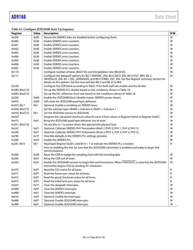
AD9166 Data Sheet
Rev. 0 | Page 68 of 138
Table 43. Configure JESD204B Start-Up Sequence Register Value Description R/W 0x300 0x00 Ensure the SERDES links are disabled before configuring them. W 0x480 0x38 Enable SERDES error counters. W 0x481 0x38 Enable SERDES error counters. W 0x482 0x38 Enable SERDES error counters. W 0x483 0x38 Enable SERDES error counters. W 0x484 0x38 Enable SERDES error counters. W 0x485 0x38 Enable SERDES error counters. W 0x486 0x38 Enable SERDES error counters. W 0x487 0x38 Enable SERDES error counters. W 0x110 Configure number of lanes (Bits[7:4]) and interpolation rate (Bits[3:0]). W 0x111 Configure the datapath options for Bit 7 (INVSINC_EN), Bit 6 (NCO_EN), Bit 4 (FILT_BW), Bit 2
(MODULUS_EN), Bit 1 (SEL_SIDEBAND), and Bit 0 (FIR85_FILT_EN). See the Register Summary section for details on the options. Set the reserved bits (Bit 5 and Bit 3) to 0b0.
W
0x230 Configure the CDR block according to Table 19 for both half rate enable and the divider. W 0x289, Bits[1:0] Set up the SERDES PLL divider based on the conditions shown in Table 18. W 0x084, Bits[5:4] Set up the PLL reference clock rate based on the conditions shown in Table 18. W 0x200 0x00 Enable the JESD204B block (disable master SERDES power-down). W 0x475 0x09 Soft reset the JESD204B quad-byte deframer. W 0x453, Bit 7 0b1 Optional. Enable scrambling on SERDES lanes. W 0x458, Bits[7:5] Set the subclass type: 0b000 = Subclass 0, 0b001 = Subclass 1. W 0x459, Bits[7:5] 0b1 Set the JESD204x version to JESD204B. W 0x45D Program the calculated checksum value for Lane 0 from values in Register 0x450 to Register 0x45C. W 0x475 0x01 Bring the JESD204B quad-byte deframer out of reset. W 0x201, Bits[7:0] Set any bits to 1 to power down the appropriate physical lane. W 0x2A7 0x01 Optional. Calibrate SERDES PHY Termination Block 1 (PHY 0, PHY 1, PHY 6, PHY 7). W 0x2AE 0x01 Optional. Calibrate SERDES PHY Termination Block 2 (PHY 2, PHY 3, PHY 4, PHY 5). W 0x29E 0x1F Override defaults in the SERDES PLL settings (private). W 0x280 0x03 Enable the SERDES PLL. W 0x281, Bit 0 0b1 Read back Register 0x281 until Bit 0 = 1 to indicate the SERDES PLL is locked. R Prior to enabling the link, be sure that the JESD204B transmitter is enabled and ready to begin link
synchronization.
0x206 0x00 Reset the CDR to realign the sampling clock with the incoming data. W 0x206 0x01 Bring the CDR out of reset. W 0x300 0x01 Enable the JESD204B receiver to begin link synchronization. When SYNCOUT± is asserted, the JESD204B
transmitter begins CGS by sending /K/ characters. W
0x470 0xFF Read the CGS status for all lanes. R 0x471 0xFF Read the frame sync status for all lanes. R 0x472 0xFF Read the good checksum status for all lanes. R 0x473 0xFF Read the initial lane sync status for all lanes. R 0x024 0x1F Clear the datapath interrupts. W 0x4BA 0xFF Clear the SERDES interrupts. W 0x4BB 0x01 Clear the SERDES interrupt. W 0x020 0x0F Optional. Enable the interrupts. W 0x4B8 0xFF Optional. Enable JESD204B interrupts. W 0x4B9 0x01 Optional. Enable JESD204B interrupts. W
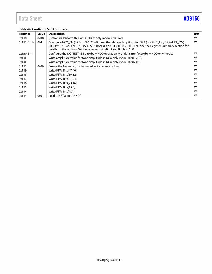
Data Sheet AD9166
Rev. 0 | Page 69 of 138
Table 44. Configure NCO Sequence Register Value Description R/W 0x110 0x80 (Optional). Perform this write if NCO only mode is desired. W 0x111, Bit 6 0b1 Configure NCO_EN (Bit 6) = 0b1. Configure other datapath options for Bit 7 (INVSINC_EN), Bit 4 (FILT_BW),
Bit 2 (MODULUS_EN), Bit 1 (SEL_SIDEBAND), and Bit 0 (FIR85_FILT_EN). See the Register Summary section for details on the options. Set the reserved bits (Bit 5 and Bit 3) to 0b0.
W
0x150, Bit 1 Configure the DC_TEST_EN bit: 0b0 = NCO operation with data interface; 0b1 = NCO only mode. W 0x14E Write amplitude value for tone amplitude in NCO only mode (Bits[15:8]). W 0x14F Write amplitude value for tone amplitude in NCO only mode (Bits[7:0]). W 0x113 0x00 Ensure the frequency tuning word write request is low. W 0x119 Write FTW, Bits[47:40]. W 0x118 Write FTW, Bits[39:32]. W 0x117 Write FTW, Bits[31:24]. W 0x116 Write FTW, Bits[23:16]. W 0x115 Write FTW, Bits[15:8]. W 0x114 Write FTW, Bits[7:0]. W 0x113 0x01 Load the FTW to the NCO. W
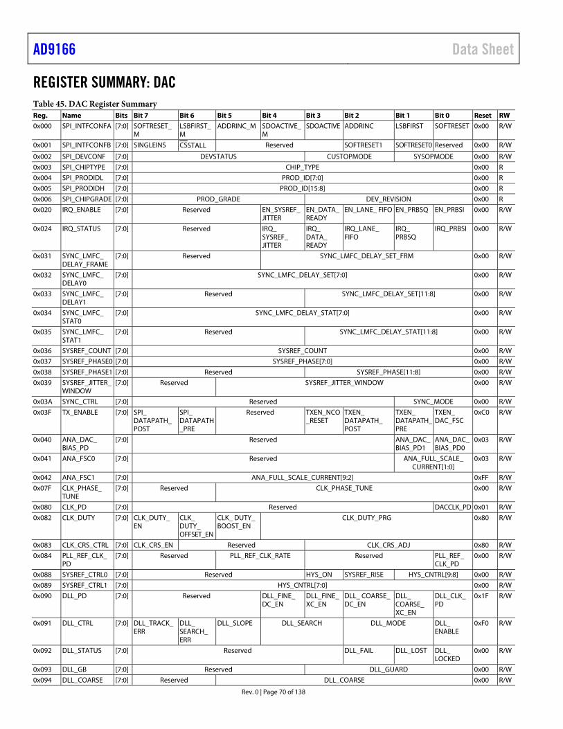
AD9166 Data Sheet
Rev. 0 | Page 70 of 138
REGISTER SUMMARY: DAC Table 45. DAC Register Summary Reg. Name Bits Bit 7 Bit 6 Bit 5 Bit 4 Bit 3 Bit 2 Bit 1 Bit 0 Reset RW
0x000 SPI_INTFCONFA [7:0] SOFTRESET_M
LSBFIRST_M
ADDRINC_M SDOACTIVE_M
SDOACTIVE ADDRINC LSBFIRST SOFTRESET 0x00 R/W
0x001 SPI_INTFCONFB [7:0] SINGLEINS CSSTALL Reserved SOFTRESET1 SOFTRESET0 Reserved 0x00 R/W
0x002 SPI_DEVCONF [7:0] DEVSTATUS CUSTOPMODE SYSOPMODE 0x00 R/W
0x003 SPI_CHIPTYPE [7:0] CHIP_TYPE 0x00 R
0x004 SPI_PRODIDL [7:0] PROD_ID[7:0] 0x00 R
0x005 SPI_PRODIDH [7:0] PROD_ID[15:8] 0x00 R
0x006 SPI_CHIPGRADE [7:0] PROD_GRADE DEV_REVISION 0x00 R
0x020 IRQ_ENABLE [7:0] Reserved EN_SYSREF_ JITTER
EN_DATA_READY
EN_LANE_ FIFO EN_PRBSQ EN_PRBSI 0x00 R/W
0x024 IRQ_STATUS [7:0] Reserved IRQ_ SYSREF_ JITTER
IRQ_ DATA_ READY
IRQ_LANE_ FIFO
IRQ_ PRBSQ
IRQ_PRBSI 0x00 R/W
0x031 SYNC_LMFC_ DELAY_FRAME
[7:0] Reserved SYNC_LMFC_DELAY_SET_FRM 0x00 R/W
0x032 SYNC_LMFC_ DELAY0
[7:0] SYNC_LMFC_DELAY_SET[7:0] 0x00 R/W
0x033 SYNC_LMFC_ DELAY1
[7:0] Reserved SYNC_LMFC_DELAY_SET[11:8] 0x00 R/W
0x034 SYNC_LMFC_ STAT0
[7:0] SYNC_LMFC_DELAY_STAT[7:0] 0x00 R/W
0x035 SYNC_LMFC_ STAT1
[7:0] Reserved SYNC_LMFC_DELAY_STAT[11:8] 0x00 R/W
0x036 SYSREF_COUNT [7:0] SYSREF_COUNT 0x00 R/W
0x037 SYSREF_PHASE0 [7:0] SYSREF_PHASE[7:0] 0x00 R/W
0x038 SYSREF_PHASE1 [7:0] Reserved SYSREF_PHASE[11:8] 0x00 R/W
0x039 SYSREF_JITTER_ WINDOW
[7:0] Reserved SYSREF_JITTER_WINDOW 0x00 R/W
0x03A SYNC_CTRL [7:0] Reserved SYNC_MODE 0x00 R/W
0x03F TX_ENABLE [7:0] SPI_ DATAPATH_ POST
SPI_ DATAPATH_PRE
Reserved TXEN_NCO_RESET
TXEN_ DATAPATH_ POST
TXEN_ DATAPATH_PRE
TXEN_ DAC_FSC
0xC0 R/W
0x040 ANA_DAC_ BIAS_PD
[7:0] Reserved ANA_DAC_BIAS_PD1
ANA_DAC_ BIAS_PD0
0x03 R/W
0x041 ANA_FSC0 [7:0] Reserved ANA_FULL_SCALE_ CURRENT[1:0]
0x03 R/W
0x042 ANA_FSC1 [7:0] ANA_FULL_SCALE_CURRENT[9:2] 0xFF R/W
0x07F CLK_PHASE_ TUNE
[7:0] Reserved CLK_PHASE_TUNE 0x00 R/W
0x080 CLK_PD [7:0] Reserved DACCLK_PD 0x01 R/W
0x082 CLK_DUTY [7:0] CLK_DUTY_ EN
CLK_ DUTY_ OFFSET_EN
CLK_ DUTY_ BOOST_EN
CLK_DUTY_PRG 0x80 R/W
0x083 CLK_CRS_CTRL [7:0] CLK_CRS_EN Reserved CLK_CRS_ADJ 0x80 R/W
0x084 PLL_REF_CLK_ PD
[7:0] Reserved PLL_REF_CLK_RATE Reserved PLL_REF_ CLK_PD
0x00 R/W
0x088 SYSREF_CTRL0 [7:0] Reserved HYS_ON SYSREF_RISE HYS_CNTRL[9:8] 0x00 R/W
0x089 SYSREF_CTRL1 [7:0] HYS_CNTRL[7:0] 0x00 R/W
0x090 DLL_PD [7:0] Reserved DLL_FINE_ DC_EN
DLL_FINE_ XC_EN
DLL_ COARSE_ DC_EN
DLL_ COARSE_ XC_EN
DLL_CLK_ PD
0x1F R/W
0x091 DLL_CTRL [7:0] DLL_TRACK_ ERR
DLL_ SEARCH_ ERR
DLL_SLOPE DLL_SEARCH DLL_MODE DLL_ ENABLE
0xF0 R/W
0x092 DLL_STATUS [7:0] Reserved DLL_FAIL DLL_LOST DLL_ LOCKED
0x00 R/W
0x093 DLL_GB [7:0] Reserved DLL_GUARD 0x00 R/W
0x094 DLL_COARSE [7:0] Reserved DLL_COARSE 0x00 R/W
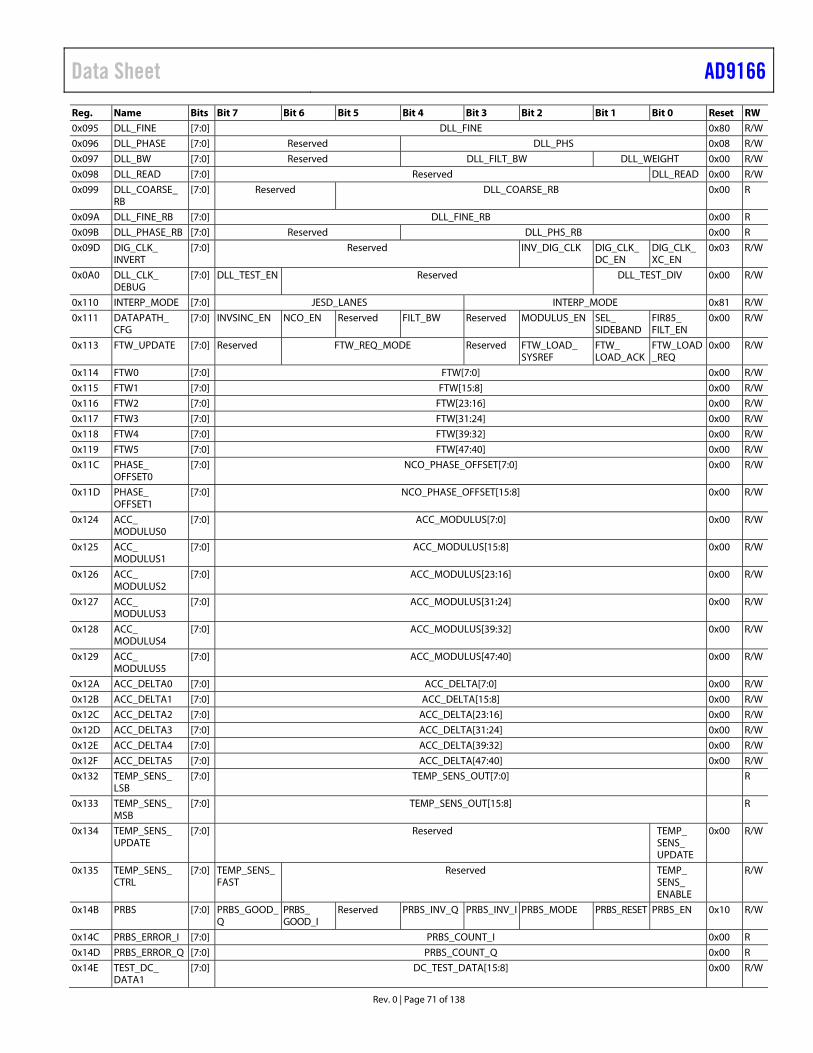
Data Sheet AD9166
Rev. 0 | Page 71 of 138
Reg. Name Bits Bit 7 Bit 6 Bit 5 Bit 4 Bit 3 Bit 2 Bit 1 Bit 0 Reset RW
0x095 DLL_FINE [7:0] DLL_FINE 0x80 R/W
0x096 DLL_PHASE [7:0] Reserved DLL_PHS 0x08 R/W
0x097 DLL_BW [7:0] Reserved DLL_FILT_BW DLL_WEIGHT 0x00 R/W
0x098 DLL_READ [7:0] Reserved DLL_READ 0x00 R/W
0x099 DLL_COARSE_ RB
[7:0] Reserved DLL_COARSE_RB 0x00 R
0x09A DLL_FINE_RB [7:0] DLL_FINE_RB 0x00 R
0x09B DLL_PHASE_RB [7:0] Reserved DLL_PHS_RB 0x00 R
0x09D DIG_CLK_ INVERT
[7:0] Reserved INV_DIG_CLK DIG_CLK_ DC_EN
DIG_CLK_ XC_EN
0x03 R/W
0x0A0 DLL_CLK_ DEBUG
[7:0] DLL_TEST_EN Reserved DLL_TEST_DIV 0x00 R/W
0x110 INTERP_MODE [7:0] JESD_LANES INTERP_MODE 0x81 R/W
0x111 DATAPATH_ CFG
[7:0] INVSINC_EN NCO_EN Reserved FILT_BW Reserved MODULUS_EN SEL_ SIDEBAND
FIR85_ FILT_EN
0x00 R/W
0x113 FTW_UPDATE [7:0] Reserved FTW_REQ_MODE Reserved FTW_LOAD_ SYSREF
FTW_ LOAD_ACK
FTW_LOAD_REQ
0x00 R/W
0x114 FTW0 [7:0] FTW[7:0] 0x00 R/W
0x115 FTW1 [7:0] FTW[15:8] 0x00 R/W
0x116 FTW2 [7:0] FTW[23:16] 0x00 R/W
0x117 FTW3 [7:0] FTW[31:24] 0x00 R/W
0x118 FTW4 [7:0] FTW[39:32] 0x00 R/W
0x119 FTW5 [7:0] FTW[47:40] 0x00 R/W
0x11C PHASE_ OFFSET0
[7:0] NCO_PHASE_OFFSET[7:0] 0x00 R/W
0x11D PHASE_ OFFSET1
[7:0] NCO_PHASE_OFFSET[15:8] 0x00 R/W
0x124 ACC_ MODULUS0
[7:0] ACC_MODULUS[7:0] 0x00 R/W
0x125 ACC_ MODULUS1
[7:0] ACC_MODULUS[15:8] 0x00 R/W
0x126 ACC_ MODULUS2
[7:0] ACC_MODULUS[23:16] 0x00 R/W
0x127 ACC_ MODULUS3
[7:0] ACC_MODULUS[31:24] 0x00 R/W
0x128 ACC_ MODULUS4
[7:0] ACC_MODULUS[39:32] 0x00 R/W
0x129 ACC_ MODULUS5
[7:0] ACC_MODULUS[47:40] 0x00 R/W
0x12A ACC_DELTA0 [7:0] ACC_DELTA[7:0] 0x00 R/W
0x12B ACC_DELTA1 [7:0] ACC_DELTA[15:8] 0x00 R/W
0x12C ACC_DELTA2 [7:0] ACC_DELTA[23:16] 0x00 R/W
0x12D ACC_DELTA3 [7:0] ACC_DELTA[31:24] 0x00 R/W
0x12E ACC_DELTA4 [7:0] ACC_DELTA[39:32] 0x00 R/W
0x12F ACC_DELTA5 [7:0] ACC_DELTA[47:40] 0x00 R/W
0x132 TEMP_SENS_ LSB
[7:0] TEMP_SENS_OUT[7:0] R
0x133 TEMP_SENS_ MSB
[7:0] TEMP_SENS_OUT[15:8] R
0x134 TEMP_SENS_ UPDATE
[7:0] Reserved TEMP_ SENS_ UPDATE
0x00 R/W
0x135 TEMP_SENS_ CTRL
[7:0] TEMP_SENS_ FAST
Reserved TEMP_ SENS_ ENABLE
R/W
0x14B PRBS [7:0] PRBS_GOOD_Q
PRBS_ GOOD_I
Reserved PRBS_INV_Q PRBS_INV_I PRBS_MODE PRBS_RESET PRBS_EN 0x10 R/W
0x14C PRBS_ERROR_I [7:0] PRBS_COUNT_I 0x00 R
0x14D PRBS_ERROR_Q [7:0] PRBS_COUNT_Q 0x00 R
0x14E TEST_DC_ DATA1
[7:0] DC_TEST_DATA[15:8] 0x00 R/W
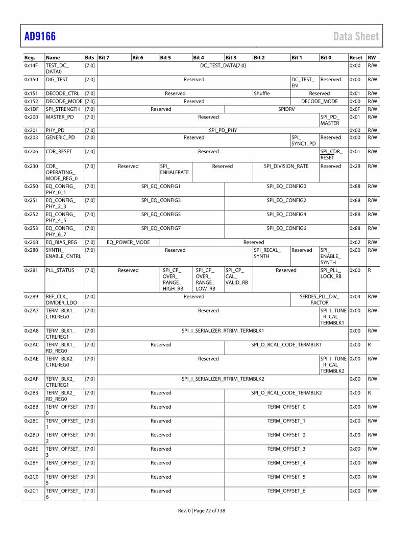
AD9166 Data Sheet
Rev. 0 | Page 72 of 138
Reg. Name Bits Bit 7 Bit 6 Bit 5 Bit 4 Bit 3 Bit 2 Bit 1 Bit 0 Reset RW
0x14F TEST_DC_ DATA0
[7:0] DC_TEST_DATA[7:0] 0x00 R/W
0x150 DIG_TEST [7:0] Reserved DC_TEST_ EN
Reserved 0x00 R/W
0x151 DECODE_CTRL [7:0] Reserved Shuffle Reserved 0x01 R/W
0x152 DECODE_MODE [7:0] Reserved DECODE_MODE 0x00 R/W
0x1DF SPI_STRENGTH [7:0] Reserved SPIDRV 0x0F R/W
0x200 MASTER_PD [7:0] Reserved SPI_PD_ MASTER
0x01 R/W
0x201 PHY_PD [7:0] SPI_PD_PHY 0x00 R/W0x203 GENERIC_PD [7:0] Reserved SPI_
SYNC1_PD Reserved 0x00 R/W
0x206 CDR_RESET [7:0] Reserved SPI_CDR_RESET
0x01 R/W
0x230 CDR_ OPERATING_ MODE_REG_0
[7:0] Reserved SPI_ ENHALFRATE
Reserved SPI_DIVISION_RATE Reserved 0x28 R/W
0x250 EQ_CONFIG_ PHY_0_1
[7:0] SPI_EQ_CONFIG1 SPI_EQ_CONFIG0 0x88 R/W
0x251 EQ_CONFIG_ PHY_2_3
[7:0] SPI_EQ_CONFIG3 SPI_EQ_CONFIG2 0x88 R/W
0x252 EQ_CONFIG_ PHY_4_5
[7:0] SPI_EQ_CONFIG5 SPI_EQ_CONFIG4 0x88 R/W
0x253 EQ_CONFIG_ PHY_6_7
[7:0] SPI_EQ_CONFIG7 SPI_EQ_CONFIG6 0x88 R/W
0x268 EQ_BIAS_REG [7:0] EQ_POWER_MODE Reserved 0x62 R/W
0x280 SYNTH_ ENABLE_CNTRL
[7:0] Reserved SPI_RECAL_ SYNTH
Reserved SPI_ ENABLE_ SYNTH
0x00 R/W
0x281 PLL_STATUS [7:0] Reserved SPI_CP_ OVER_ RANGE_ HIGH_RB
SPI_CP_ OVER_ RANGE_ LOW_RB
SPI_CP_ CAL_ VALID_RB
Reserved SPI_PLL_ LOCK_RB
0x00 R
0x289 REF_CLK_ DIVIDER_LDO
[7:0] Reserved SERDES_PLL_DIV_ FACTOR
0x04 R/W
0x2A7 TERM_BLK1_ CTRLREG0
[7:0] Reserved SPI_I_TUNE_R_CAL_ TERMBLK1
0x00 R/W
0x2A8 TERM_BLK1_ CTRLREG1
[7:0] SPI_I_SERIALIZER_RTRIM_TERMBLK1 0x00 R/W
0x2AC TERM_BLK1_ RD_REG0
[7:0] Reserved SPI_O_RCAL_CODE_TERMBLK1 0x00 R
0x2AE TERM_BLK2_ CTRLREG0
[7:0] Reserved SPI_I_TUNE_R_CAL_ TERMBLK2
0x00 R/W
0x2AF TERM_BLK2_ CTRLREG1
[7:0] SPI_I_SERIALIZER_RTRIM_TERMBLK2 0x00 R/W
0x2B3 TERM_BLK2_ RD_REG0
[7:0] Reserved SPI_O_RCAL_CODE_TERMBLK2 0x00 R
0x2BB TERM_OFFSET_0
[7:0] Reserved TERM_OFFSET_0 0x00 R/W
0x2BC TERM_OFFSET_1
[7:0] Reserved TERM_OFFSET_1 0x00 R/W
0x2BD TERM_OFFSET_2
[7:0] Reserved TERM_OFFSET_2 0x00 R/W
0x2BE TERM_OFFSET_3
[7:0] Reserved TERM_OFFSET_3 0x00 R/W
0x2BF TERM_OFFSET_4
[7:0] Reserved TERM_OFFSET_4 0x00 R/W
0x2C0 TERM_OFFSET_5
[7:0] Reserved TERM_OFFSET_5 0x00 R/W
0x2C1 TERM_OFFSET_6
[7:0] Reserved TERM_OFFSET_6 0x00 R/W
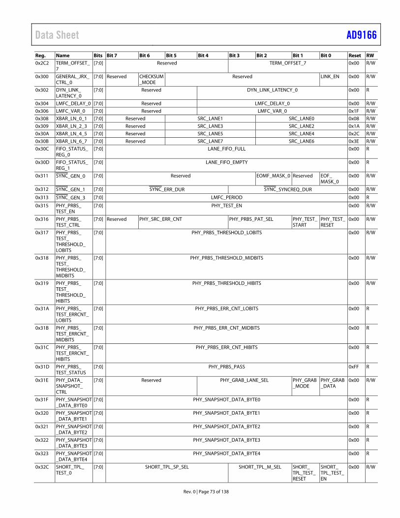
Data Sheet AD9166
Rev. 0 | Page 73 of 138
Reg. Name Bits Bit 7 Bit 6 Bit 5 Bit 4 Bit 3 Bit 2 Bit 1 Bit 0 Reset RW
0x2C2 TERM_OFFSET_7
[7:0] Reserved TERM_OFFSET_7 0x00 R/W
0x300 GENERAL_JRX_ CTRL_0
[7:0] Reserved CHECKSUM_MODE
Reserved LINK_EN 0x00 R/W
0x302 DYN_LINK_ LATENCY_0
[7:0] Reserved DYN_LINK_LATENCY_0 0x00 R
0x304 LMFC_DELAY_0 [7:0] Reserved LMFC_DELAY_0 0x00 R/W
0x306 LMFC_VAR_0 [7:0] Reserved LMFC_VAR_0 0x1F R/W
0x308 XBAR_LN_0_1 [7:0] Reserved SRC_LANE1 SRC_LANE0 0x08 R/W
0x309 XBAR_LN_2_3 [7:0] Reserved SRC_LANE3 SRC_LANE2 0x1A R/W
0x30A XBAR_LN_4_5 [7:0] Reserved SRC_LANE5 SRC_LANE4 0x2C R/W
0x30B XBAR_LN_6_7 [7:0] Reserved SRC_LANE7 SRC_LANE6 0x3E R/W
0x30C FIFO_STATUS_ REG_0
[7:0] LANE_FIFO_FULL 0x00 R
0x30D FIFO_STATUS_ REG_1
[7:0] LANE_FIFO_EMPTY 0x00 R
0x311 SYNC_GEN_0 [7:0] Reserved EOMF_MASK_0 Reserved EOF_ MASK_0
0x00 R/W
0x312 SYNC_GEN_1 [7:0] SYNC_ERR_DUR SYNC_SYNCREQ_DUR 0x00 R/W
0x313 SYNC_GEN_3 [7:0] LMFC_PERIOD 0x00 R
0x315 PHY_PRBS_ TEST_EN
[7:0] PHY_TEST_EN 0x00 R/W
0x316 PHY_PRBS_ TEST_CTRL
[7:0] Reserved PHY_SRC_ERR_CNT PHY_PRBS_PAT_SEL PHY_TEST_ START
PHY_TEST_ RESET
0x00 R/W
0x317 PHY_PRBS_ TEST_ THRESHOLD_ LOBITS
[7:0] PHY_PRBS_THRESHOLD_LOBITS 0x00 R/W
0x318 PHY_PRBS_ TEST_ THRESHOLD_ MIDBITS
[7:0] PHY_PRBS_THRESHOLD_MIDBITS 0x00 R/W
0x319 PHY_PRBS_ TEST_ THRESHOLD_ HIBITS
[7:0] PHY_PRBS_THRESHOLD_HIBITS 0x00 R/W
0x31A PHY_PRBS_ TEST_ERRCNT_ LOBITS
[7:0] PHY_PRBS_ERR_CNT_LOBITS 0x00 R
0x31B PHY_PRBS_ TEST_ERRCNT_MIDBITS
[7:0] PHY_PRBS_ERR_CNT_MIDBITS 0x00 R
0x31C PHY_PRBS_ TEST_ERRCNT_HIBITS
[7:0] PHY_PRBS_ERR_CNT_HIBITS 0x00 R
0x31D PHY_PRBS_ TEST_STATUS
[7:0] PHY_PRBS_PASS 0xFF R
0x31E PHY_DATA_ SNAPSHOT_ CTRL
[7:0] Reserved PHY_GRAB_LANE_SEL PHY_GRAB_MODE
PHY_GRAB_DATA
0x00 R/W
0x31F PHY_SNAPSHOT_DATA_BYTE0
[7:0] PHY_SNAPSHOT_DATA_BYTE0 0x00 R
0x320 PHY_SNAPSHOT_DATA_BYTE1
[7:0] PHY_SNAPSHOT_DATA_BYTE1 0x00 R
0x321 PHY_SNAPSHOT_DATA_BYTE2
[7:0] PHY_SNAPSHOT_DATA_BYTE2 0x00 R
0x322 PHY_SNAPSHOT_DATA_BYTE3
[7:0] PHY_SNAPSHOT_DATA_BYTE3 0x00 R
0x323 PHY_SNAPSHOT_DATA_BYTE4
[7:0] PHY_SNAPSHOT_DATA_BYTE4 0x00 R
0x32C SHORT_TPL_ TEST_0
[7:0] SHORT_TPL_SP_SEL SHORT_TPL_M_SEL SHORT_ TPL_TEST_ RESET
SHORT_ TPL_TEST_ EN
0x00 R/W
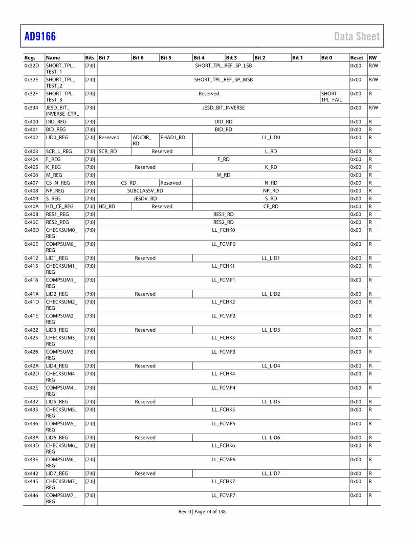
AD9166 Data Sheet
Rev. 0 | Page 74 of 138
Reg. Name Bits Bit 7 Bit 6 Bit 5 Bit 4 Bit 3 Bit 2 Bit 1 Bit 0 Reset RW
0x32D SHORT_TPL_ TEST_1
[7:0] SHORT_TPL_REF_SP_LSB 0x00 R/W
0x32E SHORT_TPL_ TEST_2
[7:0] SHORT_TPL_REF_SP_MSB 0x00 R/W
0x32F SHORT_TPL_ TEST_3
[7:0] Reserved SHORT_ TPL_FAIL
0x00 R
0x334 JESD_BIT_ INVERSE_CTRL
[7:0] JESD_BIT_INVERSE 0x00 R/W
0x400 DID_REG [7:0] DID_RD 0x00 R
0x401 BID_REG [7:0] BID_RD 0x00 R
0x402 LID0_REG [7:0] Reserved ADJDIR_ RD
PHADJ_RD LL_LID0 0x00 R
0x403 SCR_L_REG [7:0] SCR_RD Reserved L_RD 0x00 R
0x404 F_REG [7:0] F_RD 0x00 R
0x405 K_REG [7:0] Reserved K_RD 0x00 R
0x406 M_REG [7:0] M_RD 0x00 R
0x407 CS_N_REG [7:0] CS_RD Reserved N_RD 0x00 R
0x408 NP_REG [7:0] SUBCLASSV_RD NP_RD 0x00 R
0x409 S_REG [7:0] JESDV_RD S_RD 0x00 R
0x40A HD_CF_REG [7:0] HD_RD Reserved CF_RD 0x00 R
0x40B RES1_REG [7:0] RES1_RD 0x00 R
0x40C RES2_REG [7:0] RES2_RD 0x00 R
0x40D CHECKSUM0_ REG
[7:0] LL_FCHK0 0x00 R
0x40E COMPSUM0_ REG
[7:0] LL_FCMP0 0x00 R
0x412 LID1_REG [7:0] Reserved LL_LID1 0x00 R
0x415 CHECKSUM1_ REG
[7:0] LL_FCHK1 0x00 R
0x416 COMPSUM1_ REG
[7:0] LL_FCMP1 0x00 R
0x41A LID2_REG [7:0] Reserved LL_LID2 0x00 R
0x41D CHECKSUM2_ REG
[7:0] LL_FCHK2 0x00 R
0x41E COMPSUM2_ REG
[7:0] LL_FCMP2 0x00 R
0x422 LID3_REG [7:0] Reserved LL_LID3 0x00 R
0x425 CHECKSUM3_ REG
[7:0] LL_FCHK3 0x00 R
0x426 COMPSUM3_ REG
[7:0] LL_FCMP3 0x00 R
0x42A LID4_REG [7:0] Reserved LL_LID4 0x00 R
0x42D CHECKSUM4_ REG
[7:0] LL_FCHK4 0x00 R
0x42E COMPSUM4_ REG
[7:0] LL_FCMP4 0x00 R
0x432 LID5_REG [7:0] Reserved LL_LID5 0x00 R
0x435 CHECKSUM5_ REG
[7:0] LL_FCHK5 0x00 R
0x436 COMPSUM5_ REG
[7:0] LL_FCMP5 0x00 R
0x43A LID6_REG [7:0] Reserved LL_LID6 0x00 R
0x43D CHECKSUM6_ REG
[7:0] LL_FCHK6 0x00 R
0x43E COMPSUM6_ REG
[7:0] LL_FCMP6 0x00 R
0x442 LID7_REG [7:0] Reserved LL_LID7 0x00 R
0x445 CHECKSUM7_ REG
[7:0] LL_FCHK7 0x00 R
0x446 COMPSUM7_ REG
[7:0] LL_FCMP7 0x00 R
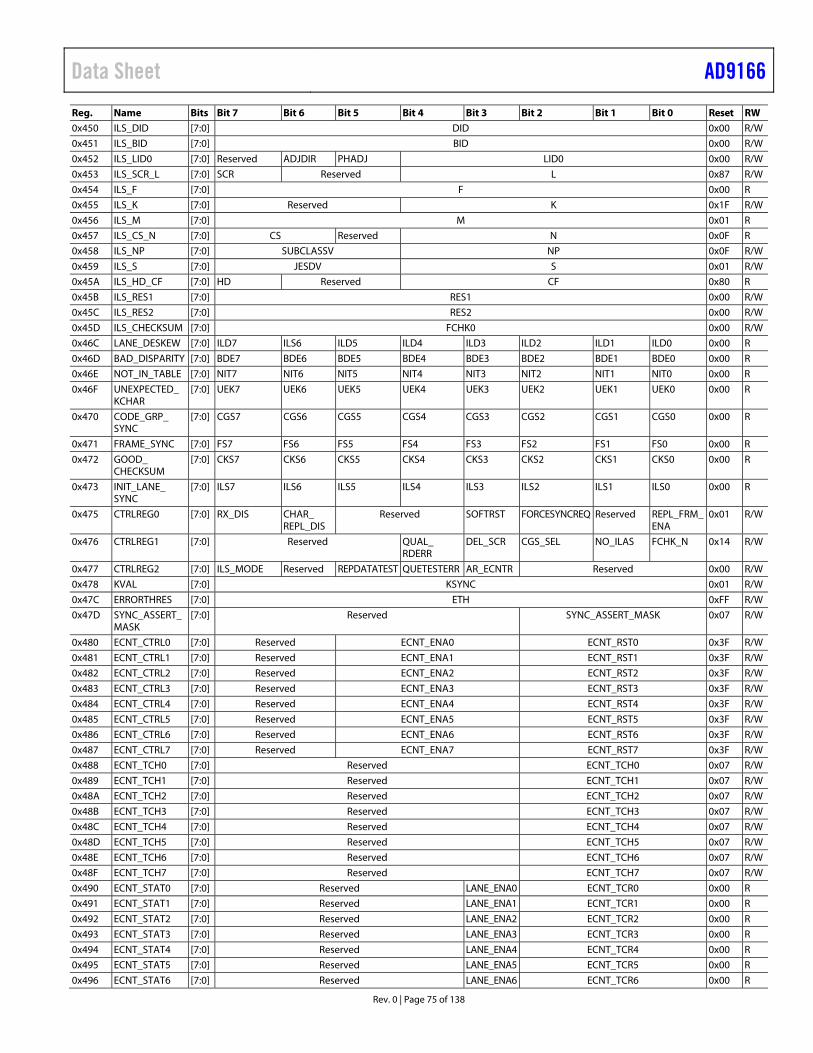
Data Sheet AD9166
Rev. 0 | Page 75 of 138
Reg. Name Bits Bit 7 Bit 6 Bit 5 Bit 4 Bit 3 Bit 2 Bit 1 Bit 0 Reset RW
0x450 ILS_DID [7:0] DID 0x00 R/W
0x451 ILS_BID [7:0] BID 0x00 R/W
0x452 ILS_LID0 [7:0] Reserved ADJDIR PHADJ LID0 0x00 R/W
0x453 ILS_SCR_L [7:0] SCR Reserved L 0x87 R/W
0x454 ILS_F [7:0] F 0x00 R
0x455 ILS_K [7:0] Reserved K 0x1F R/W
0x456 ILS_M [7:0] M 0x01 R
0x457 ILS_CS_N [7:0] CS Reserved N 0x0F R
0x458 ILS_NP [7:0] SUBCLASSV NP 0x0F R/W
0x459 ILS_S [7:0] JESDV S 0x01 R/W
0x45A ILS_HD_CF [7:0] HD Reserved CF 0x80 R
0x45B ILS_RES1 [7:0] RES1 0x00 R/W
0x45C ILS_RES2 [7:0] RES2 0x00 R/W
0x45D ILS_CHECKSUM [7:0] FCHK0 0x00 R/W
0x46C LANE_DESKEW [7:0] ILD7 ILS6 ILD5 ILD4 ILD3 ILD2 ILD1 ILD0 0x00 R
0x46D BAD_DISPARITY [7:0] BDE7 BDE6 BDE5 BDE4 BDE3 BDE2 BDE1 BDE0 0x00 R
0x46E NOT_IN_TABLE [7:0] NIT7 NIT6 NIT5 NIT4 NIT3 NIT2 NIT1 NIT0 0x00 R
0x46F UNEXPECTED_ KCHAR
[7:0] UEK7 UEK6 UEK5 UEK4 UEK3 UEK2 UEK1 UEK0 0x00 R
0x470 CODE_GRP_ SYNC
[7:0] CGS7 CGS6 CGS5 CGS4 CGS3 CGS2 CGS1 CGS0 0x00 R
0x471 FRAME_SYNC [7:0] FS7 FS6 FS5 FS4 FS3 FS2 FS1 FS0 0x00 R
0x472 GOOD_ CHECKSUM
[7:0] CKS7 CKS6 CKS5 CKS4 CKS3 CKS2 CKS1 CKS0 0x00 R
0x473 INIT_LANE_ SYNC
[7:0] ILS7 ILS6 ILS5 ILS4 ILS3 ILS2 ILS1 ILS0 0x00 R
0x475 CTRLREG0 [7:0] RX_DIS CHAR_ REPL_DIS
Reserved SOFTRST FORCESYNCREQ Reserved REPL_FRM_ ENA
0x01 R/W
0x476 CTRLREG1 [7:0] Reserved QUAL_ RDERR
DEL_SCR CGS_SEL NO_ILAS FCHK_N 0x14 R/W
0x477 CTRLREG2 [7:0] ILS_MODE Reserved REPDATATEST QUETESTERR AR_ECNTR Reserved 0x00 R/W
0x478 KVAL [7:0] KSYNC 0x01 R/W
0x47C ERRORTHRES [7:0] ETH 0xFF R/W
0x47D SYNC_ASSERT_ MASK
[7:0] Reserved SYNC_ASSERT_MASK 0x07 R/W
0x480 ECNT_CTRL0 [7:0] Reserved ECNT_ENA0 ECNT_RST0 0x3F R/W
0x481 ECNT_CTRL1 [7:0] Reserved ECNT_ENA1 ECNT_RST1 0x3F R/W
0x482 ECNT_CTRL2 [7:0] Reserved ECNT_ENA2 ECNT_RST2 0x3F R/W
0x483 ECNT_CTRL3 [7:0] Reserved ECNT_ENA3 ECNT_RST3 0x3F R/W
0x484 ECNT_CTRL4 [7:0] Reserved ECNT_ENA4 ECNT_RST4 0x3F R/W
0x485 ECNT_CTRL5 [7:0] Reserved ECNT_ENA5 ECNT_RST5 0x3F R/W
0x486 ECNT_CTRL6 [7:0] Reserved ECNT_ENA6 ECNT_RST6 0x3F R/W
0x487 ECNT_CTRL7 [7:0] Reserved ECNT_ENA7 ECNT_RST7 0x3F R/W
0x488 ECNT_TCH0 [7:0] Reserved ECNT_TCH0 0x07 R/W
0x489 ECNT_TCH1 [7:0] Reserved ECNT_TCH1 0x07 R/W
0x48A ECNT_TCH2 [7:0] Reserved ECNT_TCH2 0x07 R/W
0x48B ECNT_TCH3 [7:0] Reserved ECNT_TCH3 0x07 R/W
0x48C ECNT_TCH4 [7:0] Reserved ECNT_TCH4 0x07 R/W
0x48D ECNT_TCH5 [7:0] Reserved ECNT_TCH5 0x07 R/W
0x48E ECNT_TCH6 [7:0] Reserved ECNT_TCH6 0x07 R/W
0x48F ECNT_TCH7 [7:0] Reserved ECNT_TCH7 0x07 R/W
0x490 ECNT_STAT0 [7:0] Reserved LANE_ENA0 ECNT_TCR0 0x00 R
0x491 ECNT_STAT1 [7:0] Reserved LANE_ENA1 ECNT_TCR1 0x00 R
0x492 ECNT_STAT2 [7:0] Reserved LANE_ENA2 ECNT_TCR2 0x00 R
0x493 ECNT_STAT3 [7:0] Reserved LANE_ENA3 ECNT_TCR3 0x00 R
0x494 ECNT_STAT4 [7:0] Reserved LANE_ENA4 ECNT_TCR4 0x00 R
0x495 ECNT_STAT5 [7:0] Reserved LANE_ENA5 ECNT_TCR5 0x00 R
0x496 ECNT_STAT6 [7:0] Reserved LANE_ENA6 ECNT_TCR6 0x00 R
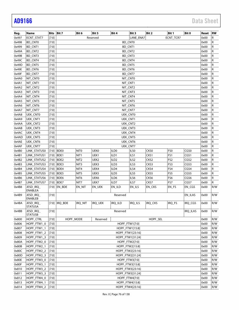
AD9166 Data Sheet
Rev. 0 | Page 76 of 138
Reg. Name Bits Bit 7 Bit 6 Bit 5 Bit 4 Bit 3 Bit 2 Bit 1 Bit 0 Reset RW
0x497 ECNT_STAT7 [7:0] Reserved LANE_ENA7 ECNT_TCR7 0x00 R
0x498 BD_CNT0 [7:0] BD_CNT0 0x00 R
0x499 BD_CNT1 [7:0] BD_CNT1 0x00 R
0x49A BD_CNT2 [7:0] BD_CNT2 0x00 R
0x49B BD_CNT3 [7:0] BD_CNT3 0x00 R
0x49C BD_CNT4 [7:0] BD_CNT4 0x00 R
0x49D BD_CNT5 [7:0] BD_CNT5 0x00 R
0x49E BD_CNT6 [7:0] BD_CNT6 0x00 R
0x49F BD_CNT7 [7:0] BD_CNT7 0x00 R
0x4A0 NIT_CNT0 [7:0] NIT_CNT0 0x00 R
0x4A1 NIT_CNT1 [7:0] NIT_CNT1 0x00 R
0x4A2 NIT_CNT2 [7:0] NIT_CNT2 0x00 R
0x4A3 NIT_CNT3 [7:0] NIT_CNT3 0x00 R
0x4A4 NIT_CNT4 [7:0] NIT_CNT4 0x00 R
0x4A5 NIT_CNT5 [7:0] NIT_CNT5 0x00 R
0x4A6 NIT_CNT6 [7:0] NIT_CNT6 0x00 R
0x4A7 NIT_CNT7 [7:0] NIT_CNT7 0x00 R
0x4A8 UEK_CNT0 [7:0] UEK_CNT0 0x00 R
0x4A9 UEK_CNT1 [7:0] UEK_CNT1 0x00 R
0x4AA UEK_CNT2 [7:0] UEK_CNT2 0x00 R
0x4AB UEK_CNT3 [7:0] UEK_CNT3 0x00 R
0x4AC UEK_CNT4 [7:0] UEK_CNT4 0x00 R
0x4AD UEK_CNT5 [7:0] UEK_CNT5 0x00 R
0x4AE UEK_CNT6 [7:0] UEK_CNT6 0x00 R
0x4AF UEK_CNT7 [7:0] UEK_CNT7 0x00 R
0x4B0 LINK_STATUS0 [7:0] BDE0 NIT0 UEK0 ILD0 ILS0 CKS0 FS0 CGS0 0x00 R
0x4B1 LINK_STATUS1 [7:0] BDE1 NIT1 UEK1 ILD1 ILS1 CKS1 FS1 CGS1 0x00 R
0x4B2 LINK_STATUS2 [7:0] BDE2 NIT2 UEK2 ILD2 ILS2 CKS2 FS2 CGS2 0x00 R
0x4B3 LINK_STATUS3 [7:0] BDE3 NIT3 UEK3 ILD3 ILS3 CKS3 FS3 CGS3 0x00 R
0x4B4 LINK_STATUS4 [7:0] BDE4 NIT4 UEK4 ILD4 ILS4 CKS4 FS4 CGS4 0x00 R
0x4B5 LINK_STATUS5 [7:0] BDE5 NIT5 UEK5 ILD5 ILS5 CKS5 FS5 CGS5 0x00 R
0x4B6 LINK_STATUS6 [7:0] BDE6 NIT6 UEK6 ILD6 ILS6 CKS6 FS6 CGS6 0x00 R
0x4B7 LINK_STATUS7 [7:0] BDE7 NIT7 UEK7 ILD7 ILS7 CKS7 FS7 CGS7 0x00 R
0x4B8 JESD_IRQ_ ENABLEA
[7:0] EN_BDE EN_NIT EN_UEK EN_ILD EN_ILS EN_CKS EN_FS EN_CGS 0x00 R/W
0x4B9 JESD_IRQ_ ENABLEB
[7:0] Reserved EN_ILAS 0x00 R/W
0x4BA JESD_IRQ_ STATUSA
[7:0] IRQ_BDE IRQ_NIT IRQ_UEK IRQ_ILD IRQ_ILS IRQ_CKS IRQ_FS IRQ_CGS 0x00 R/W
0x4BB JESD_IRQ_ STATUSB
[7:0] Reserved IRQ_ILAS 0x00 R/W
0x800 HOPF_CTRL [7:0] HOPF_MODE Reserved HOPF_SEL 0x00 R/W
0x806 HOPF_FTW1_0 [7:0] HOPF_FTW1[7:0] 0x00 R/W
0x807 HOPF_FTW1_1 [7:0] HOPF_FTW1[15:8] 0x00 R/W
0x808 HOPF_FTW1_2 [7:0] HOPF_FTW1[23:16] 0x00 R/W
0x809 HOPF_FTW1_3 [7:0] HOPF_FTW1[31:24] 0x00 R/W
0x80A HOPF_FTW2_0 [7:0] HOPF_FTW2[7:0] 0x00 R/W
0x80B HOPF_FTW2_1 [7:0] HOPF_FTW2[15:8] 0x00 R/W
0x80C HOPF_FTW2_2 [7:0] HOPF_FTW2[23:16] 0x00 R/W
0x80D HOPF_FTW2_3 [7:0] HOPF_FTW2[31:24] 0x00 R/W
0x80E HOPF_FTW3_0 [7:0] HOPF_FTW3[7:0] 0x00 R/W
0x80F HOPF_FTW3_1 [7:0] HOPF_FTW3[15:8] 0x00 R/W
0x810 HOPF_FTW3_2 [7:0] HOPF_FTW3[23:16] 0x00 R/W
0x811 HOPF_FTW3_3 [7:0] HOPF_FTW3[31:24] 0x00 R/W
0x812 HOPF_FTW4_0 [7:0] HOPF_FTW4[7:0] 0x00 R/W
0x813 HOPF_FTW4_1 [7:0] HOPF_FTW4[15:8] 0x00 R/W
0x814 HOPF_FTW4_2 [7:0] HOPF_FTW4[23:16] 0x00 R/W
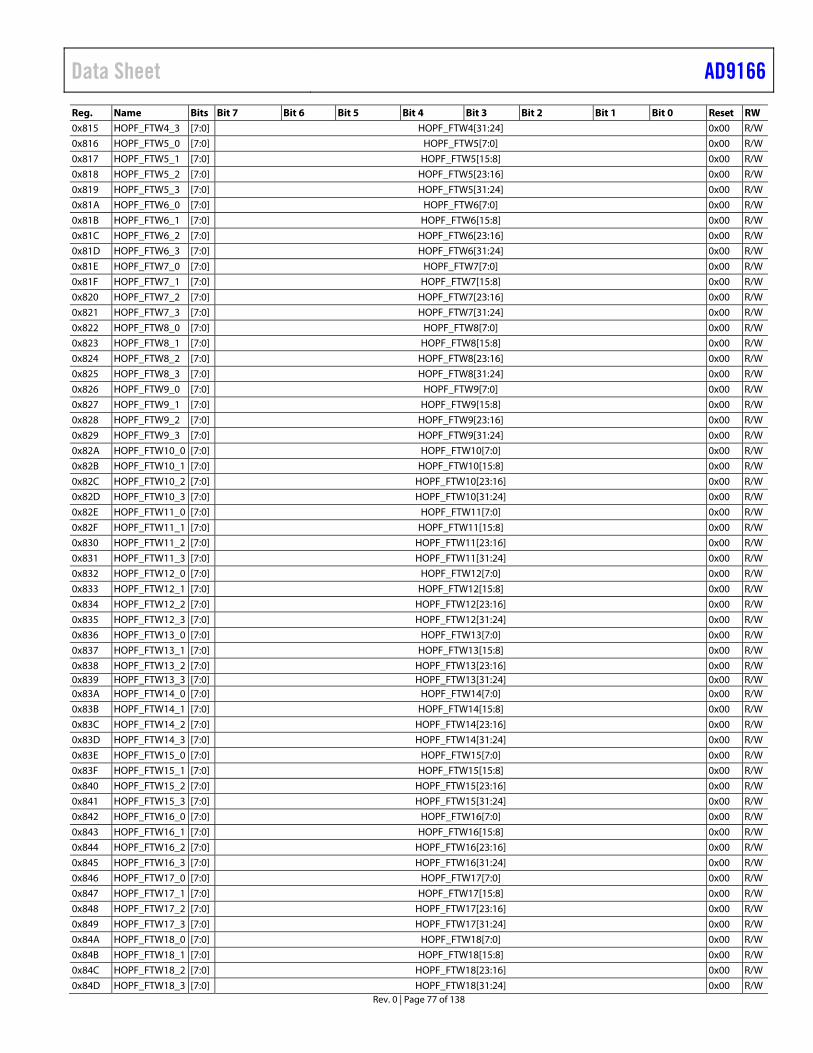
Data Sheet AD9166
Rev. 0 | Page 77 of 138
Reg. Name Bits Bit 7 Bit 6 Bit 5 Bit 4 Bit 3 Bit 2 Bit 1 Bit 0 Reset RW
0x815 HOPF_FTW4_3 [7:0] HOPF_FTW4[31:24] 0x00 R/W
0x816 HOPF_FTW5_0 [7:0] HOPF_FTW5[7:0] 0x00 R/W
0x817 HOPF_FTW5_1 [7:0] HOPF_FTW5[15:8] 0x00 R/W
0x818 HOPF_FTW5_2 [7:0] HOPF_FTW5[23:16] 0x00 R/W
0x819 HOPF_FTW5_3 [7:0] HOPF_FTW5[31:24] 0x00 R/W
0x81A HOPF_FTW6_0 [7:0] HOPF_FTW6[7:0] 0x00 R/W
0x81B HOPF_FTW6_1 [7:0] HOPF_FTW6[15:8] 0x00 R/W
0x81C HOPF_FTW6_2 [7:0] HOPF_FTW6[23:16] 0x00 R/W
0x81D HOPF_FTW6_3 [7:0] HOPF_FTW6[31:24] 0x00 R/W
0x81E HOPF_FTW7_0 [7:0] HOPF_FTW7[7:0] 0x00 R/W
0x81F HOPF_FTW7_1 [7:0] HOPF_FTW7[15:8] 0x00 R/W
0x820 HOPF_FTW7_2 [7:0] HOPF_FTW7[23:16] 0x00 R/W
0x821 HOPF_FTW7_3 [7:0] HOPF_FTW7[31:24] 0x00 R/W
0x822 HOPF_FTW8_0 [7:0] HOPF_FTW8[7:0] 0x00 R/W
0x823 HOPF_FTW8_1 [7:0] HOPF_FTW8[15:8] 0x00 R/W
0x824 HOPF_FTW8_2 [7:0] HOPF_FTW8[23:16] 0x00 R/W
0x825 HOPF_FTW8_3 [7:0] HOPF_FTW8[31:24] 0x00 R/W
0x826 HOPF_FTW9_0 [7:0] HOPF_FTW9[7:0] 0x00 R/W
0x827 HOPF_FTW9_1 [7:0] HOPF_FTW9[15:8] 0x00 R/W
0x828 HOPF_FTW9_2 [7:0] HOPF_FTW9[23:16] 0x00 R/W
0x829 HOPF_FTW9_3 [7:0] HOPF_FTW9[31:24] 0x00 R/W
0x82A HOPF_FTW10_0 [7:0] HOPF_FTW10[7:0] 0x00 R/W
0x82B HOPF_FTW10_1 [7:0] HOPF_FTW10[15:8] 0x00 R/W
0x82C HOPF_FTW10_2 [7:0] HOPF_FTW10[23:16] 0x00 R/W
0x82D HOPF_FTW10_3 [7:0] HOPF_FTW10[31:24] 0x00 R/W
0x82E HOPF_FTW11_0 [7:0] HOPF_FTW11[7:0] 0x00 R/W
0x82F HOPF_FTW11_1 [7:0] HOPF_FTW11[15:8] 0x00 R/W
0x830 HOPF_FTW11_2 [7:0] HOPF_FTW11[23:16] 0x00 R/W
0x831 HOPF_FTW11_3 [7:0] HOPF_FTW11[31:24] 0x00 R/W
0x832 HOPF_FTW12_0 [7:0] HOPF_FTW12[7:0] 0x00 R/W
0x833 HOPF_FTW12_1 [7:0] HOPF_FTW12[15:8] 0x00 R/W
0x834 HOPF_FTW12_2 [7:0] HOPF_FTW12[23:16] 0x00 R/W
0x835 HOPF_FTW12_3 [7:0] HOPF_FTW12[31:24] 0x00 R/W
0x836 HOPF_FTW13_0 [7:0] HOPF_FTW13[7:0] 0x00 R/W
0x837 HOPF_FTW13_1 [7:0] HOPF_FTW13[15:8] 0x00 R/W
0x838 HOPF_FTW13_2 [7:0] HOPF_FTW13[23:16] 0x00 R/W0x839 HOPF_FTW13_3 [7:0] HOPF_FTW13[31:24] 0x00 R/W0x83A HOPF_FTW14_0 [7:0] HOPF_FTW14[7:0] 0x00 R/W
0x83B HOPF_FTW14_1 [7:0] HOPF_FTW14[15:8] 0x00 R/W
0x83C HOPF_FTW14_2 [7:0] HOPF_FTW14[23:16] 0x00 R/W
0x83D HOPF_FTW14_3 [7:0] HOPF_FTW14[31:24] 0x00 R/W
0x83E HOPF_FTW15_0 [7:0] HOPF_FTW15[7:0] 0x00 R/W
0x83F HOPF_FTW15_1 [7:0] HOPF_FTW15[15:8] 0x00 R/W
0x840 HOPF_FTW15_2 [7:0] HOPF_FTW15[23:16] 0x00 R/W
0x841 HOPF_FTW15_3 [7:0] HOPF_FTW15[31:24] 0x00 R/W
0x842 HOPF_FTW16_0 [7:0] HOPF_FTW16[7:0] 0x00 R/W
0x843 HOPF_FTW16_1 [7:0] HOPF_FTW16[15:8] 0x00 R/W
0x844 HOPF_FTW16_2 [7:0] HOPF_FTW16[23:16] 0x00 R/W
0x845 HOPF_FTW16_3 [7:0] HOPF_FTW16[31:24] 0x00 R/W
0x846 HOPF_FTW17_0 [7:0] HOPF_FTW17[7:0] 0x00 R/W
0x847 HOPF_FTW17_1 [7:0] HOPF_FTW17[15:8] 0x00 R/W
0x848 HOPF_FTW17_2 [7:0] HOPF_FTW17[23:16] 0x00 R/W
0x849 HOPF_FTW17_3 [7:0] HOPF_FTW17[31:24] 0x00 R/W
0x84A HOPF_FTW18_0 [7:0] HOPF_FTW18[7:0] 0x00 R/W
0x84B HOPF_FTW18_1 [7:0] HOPF_FTW18[15:8] 0x00 R/W
0x84C HOPF_FTW18_2 [7:0] HOPF_FTW18[23:16] 0x00 R/W
0x84D HOPF_FTW18_3 [7:0] HOPF_FTW18[31:24] 0x00 R/W
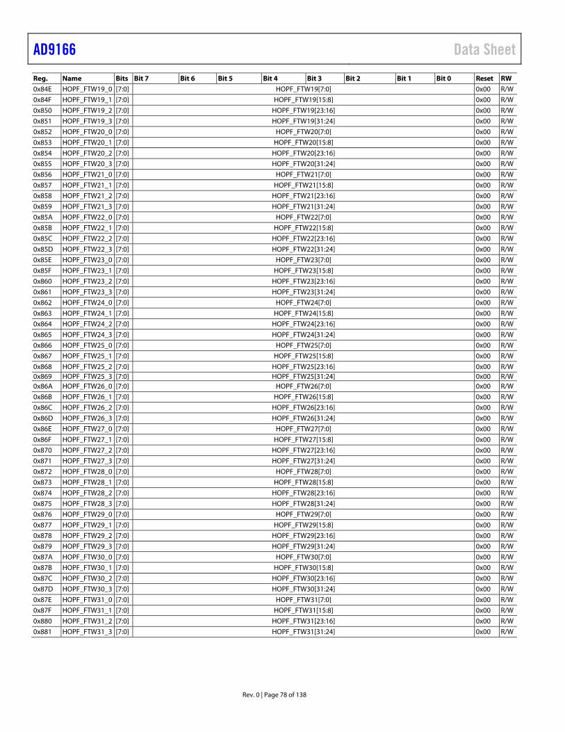
AD9166 Data Sheet
Rev. 0 | Page 78 of 138
Reg. Name Bits Bit 7 Bit 6 Bit 5 Bit 4 Bit 3 Bit 2 Bit 1 Bit 0 Reset RW
0x84E HOPF_FTW19_0 [7:0] HOPF_FTW19[7:0] 0x00 R/W
0x84F HOPF_FTW19_1 [7:0] HOPF_FTW19[15:8] 0x00 R/W
0x850 HOPF_FTW19_2 [7:0] HOPF_FTW19[23:16] 0x00 R/W
0x851 HOPF_FTW19_3 [7:0] HOPF_FTW19[31:24] 0x00 R/W
0x852 HOPF_FTW20_0 [7:0] HOPF_FTW20[7:0] 0x00 R/W
0x853 HOPF_FTW20_1 [7:0] HOPF_FTW20[15:8] 0x00 R/W
0x854 HOPF_FTW20_2 [7:0] HOPF_FTW20[23:16] 0x00 R/W
0x855 HOPF_FTW20_3 [7:0] HOPF_FTW20[31:24] 0x00 R/W
0x856 HOPF_FTW21_0 [7:0] HOPF_FTW21[7:0] 0x00 R/W
0x857 HOPF_FTW21_1 [7:0] HOPF_FTW21[15:8] 0x00 R/W
0x858 HOPF_FTW21_2 [7:0] HOPF_FTW21[23:16] 0x00 R/W
0x859 HOPF_FTW21_3 [7:0] HOPF_FTW21[31:24] 0x00 R/W
0x85A HOPF_FTW22_0 [7:0] HOPF_FTW22[7:0] 0x00 R/W
0x85B HOPF_FTW22_1 [7:0] HOPF_FTW22[15:8] 0x00 R/W
0x85C HOPF_FTW22_2 [7:0] HOPF_FTW22[23:16] 0x00 R/W
0x85D HOPF_FTW22_3 [7:0] HOPF_FTW22[31:24] 0x00 R/W
0x85E HOPF_FTW23_0 [7:0] HOPF_FTW23[7:0] 0x00 R/W
0x85F HOPF_FTW23_1 [7:0] HOPF_FTW23[15:8] 0x00 R/W
0x860 HOPF_FTW23_2 [7:0] HOPF_FTW23[23:16] 0x00 R/W
0x861 HOPF_FTW23_3 [7:0] HOPF_FTW23[31:24] 0x00 R/W
0x862 HOPF_FTW24_0 [7:0] HOPF_FTW24[7:0] 0x00 R/W
0x863 HOPF_FTW24_1 [7:0] HOPF_FTW24[15:8] 0x00 R/W
0x864 HOPF_FTW24_2 [7:0] HOPF_FTW24[23:16] 0x00 R/W
0x865 HOPF_FTW24_3 [7:0] HOPF_FTW24[31:24] 0x00 R/W
0x866 HOPF_FTW25_0 [7:0] HOPF_FTW25[7:0] 0x00 R/W
0x867 HOPF_FTW25_1 [7:0] HOPF_FTW25[15:8] 0x00 R/W
0x868 HOPF_FTW25_2 [7:0] HOPF_FTW25[23:16] 0x00 R/W0x869 HOPF_FTW25_3 [7:0] HOPF_FTW25[31:24] 0x00 R/W0x86A HOPF_FTW26_0 [7:0] HOPF_FTW26[7:0] 0x00 R/W
0x86B HOPF_FTW26_1 [7:0] HOPF_FTW26[15:8] 0x00 R/W
0x86C HOPF_FTW26_2 [7:0] HOPF_FTW26[23:16] 0x00 R/W
0x86D HOPF_FTW26_3 [7:0] HOPF_FTW26[31:24] 0x00 R/W
0x86E HOPF_FTW27_0 [7:0] HOPF_FTW27[7:0] 0x00 R/W
0x86F HOPF_FTW27_1 [7:0] HOPF_FTW27[15:8] 0x00 R/W
0x870 HOPF_FTW27_2 [7:0] HOPF_FTW27[23:16] 0x00 R/W
0x871 HOPF_FTW27_3 [7:0] HOPF_FTW27[31:24] 0x00 R/W
0x872 HOPF_FTW28_0 [7:0] HOPF_FTW28[7:0] 0x00 R/W
0x873 HOPF_FTW28_1 [7:0] HOPF_FTW28[15:8] 0x00 R/W
0x874 HOPF_FTW28_2 [7:0] HOPF_FTW28[23:16] 0x00 R/W
0x875 HOPF_FTW28_3 [7:0] HOPF_FTW28[31:24] 0x00 R/W
0x876 HOPF_FTW29_0 [7:0] HOPF_FTW29[7:0] 0x00 R/W
0x877 HOPF_FTW29_1 [7:0] HOPF_FTW29[15:8] 0x00 R/W
0x878 HOPF_FTW29_2 [7:0] HOPF_FTW29[23:16] 0x00 R/W
0x879 HOPF_FTW29_3 [7:0] HOPF_FTW29[31:24] 0x00 R/W
0x87A HOPF_FTW30_0 [7:0] HOPF_FTW30[7:0] 0x00 R/W
0x87B HOPF_FTW30_1 [7:0] HOPF_FTW30[15:8] 0x00 R/W
0x87C HOPF_FTW30_2 [7:0] HOPF_FTW30[23:16] 0x00 R/W
0x87D HOPF_FTW30_3 [7:0] HOPF_FTW30[31:24] 0x00 R/W
0x87E HOPF_FTW31_0 [7:0] HOPF_FTW31[7:0] 0x00 R/W
0x87F HOPF_FTW31_1 [7:0] HOPF_FTW31[15:8] 0x00 R/W
0x880 HOPF_FTW31_2 [7:0] HOPF_FTW31[23:16] 0x00 R/W
0x881 HOPF_FTW31_3 [7:0] HOPF_FTW31[31:24] 0x00 R/W
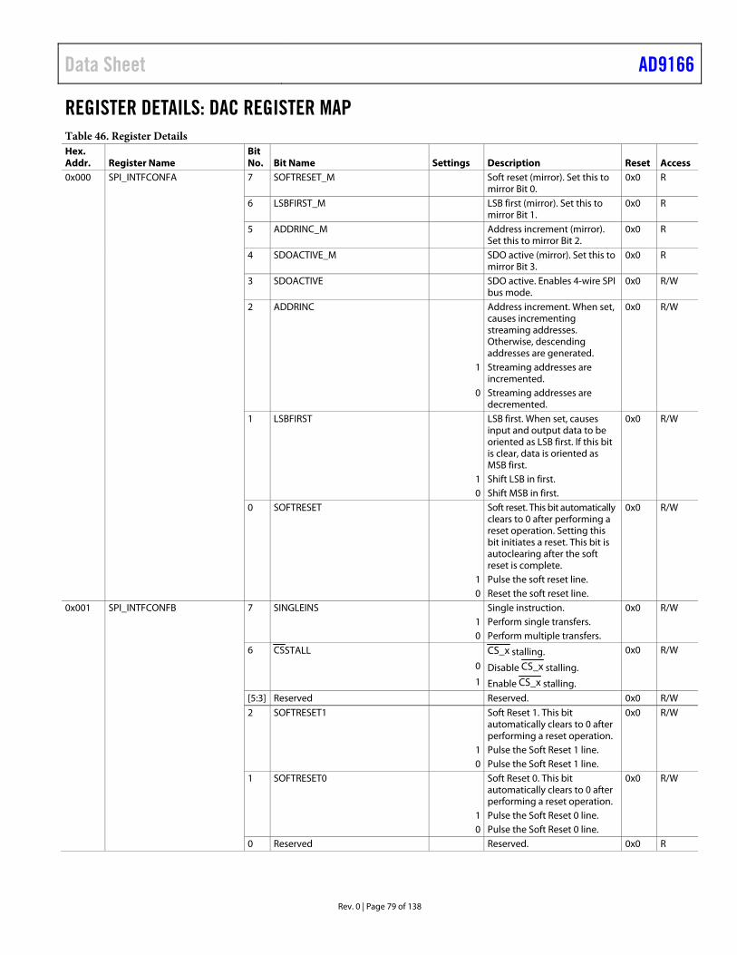
Data Sheet AD9166
Rev. 0 | Page 79 of 138
REGISTER DETAILS: DAC REGISTER MAP Table 46. Register Details Hex. Addr. Register Name
Bit No. Bit Name Settings Description Reset Access
0x000 SPI_INTFCONFA 7 SOFTRESET_M Soft reset (mirror). Set this to mirror Bit 0.
0x0 R
6 LSBFIRST_M LSB first (mirror). Set this to mirror Bit 1.
0x0 R
5 ADDRINC_M Address increment (mirror). Set this to mirror Bit 2.
0x0 R
4 SDOACTIVE_M SDO active (mirror). Set this to mirror Bit 3.
0x0 R
3 SDOACTIVE SDO active. Enables 4-wire SPI bus mode.
0x0 R/W
2 ADDRINC Address increment. When set, causes incrementing streaming addresses. Otherwise, descending addresses are generated.
0x0 R/W
1 Streaming addresses are incremented.
0 Streaming addresses are decremented.
1 LSBFIRST LSB first. When set, causes input and output data to be oriented as LSB first. If this bit is clear, data is oriented as MSB first.
0x0 R/W
1 Shift LSB in first. 0 Shift MSB in first. 0 SOFTRESET Soft reset. This bit automatically
clears to 0 after performing a reset operation. Setting this bit initiates a reset. This bit is autoclearing after the soft reset is complete.
0x0 R/W
1 Pulse the soft reset line. 0 Reset the soft reset line. 0x001 SPI_INTFCONFB 7 SINGLEINS Single instruction. 0x0 R/W 1 Perform single transfers. 0 Perform multiple transfers. 6 CSSTALL CS_x stalling. 0x0 R/W
0 Disable CS_x stalling.
1 Enable CS_x stalling.
[5:3] Reserved Reserved. 0x0 R/W
2 SOFTRESET1 Soft Reset 1. This bit automatically clears to 0 after performing a reset operation.
0x0 R/W
1 Pulse the Soft Reset 1 line. 0 Pulse the Soft Reset 1 line. 1 SOFTRESET0 Soft Reset 0. This bit
automatically clears to 0 after performing a reset operation.
0x0 R/W
1 Pulse the Soft Reset 0 line. 0 Pulse the Soft Reset 0 line. 0 Reserved Reserved. 0x0 R
AD9166 Data Sheet
Rev. 0 | Page 80 of 138
Hex. Addr. Register Name
Bit No. Bit Name Settings Description Reset Access
0x002 SPI_DEVCONF [7:4] DEVSTATUS Device status. 0x0 R/W [3:2] CUSTOPMODE Customer operating mode. 0x0 R/W
[1:0] SYSOPMODE System operating mode. 0x0 R/W 0 Normal operation. 1 Low power operation. 2 Medium power standby. 3 Low power sleep. 0x003 SPI_CHIPTYPE [7:0] CHIP_TYPE Chip type. 0x0 R 0x004 SPI_PRODIDL [7:0] PROD_ID[7:0] Product ID. 0x0 R 0x005 SPI_PRODIDH [7:0] PROD_ID[15:8] Product ID. 0x0 R 0x006 SPI_CHIPGRADE [7:4] PROD_GRADE Product grade. 0x0 R [3:0] DEV_REVISION Device revision. 0x0 R 0x020 IRQ_ENABLE [7:5] Reserved Reserved. 0x0 R 4 EN_SYSREF_JITTER Enable SYSREF± jitter interrupt. 0x0 R/W 0 Disable interrupt. 1 Enable interrupt. 3 EN_DATA_READY Enable JESD204x receiver
ready (JRX_DATA_READY) low interrupt.
0x0 R/W
0 Disable interrupt. 1 Enable interrupt. 2 EN_LANE_FIFO Enable lane FIFO overflow/
underflow interrupt. 0x0 R/W
0 Disable interrupt. 1 Enable interrupt. 1 EN_PRBSQ Enable PRBS imaginary error
interrupt. 0x0 R/W
0 Disable interrupt. 1 Enable interrupt. 0 EN_PRBSI Enable PRBS real error
interrupt. 0x0 R/W
0 Disable interrupt. 1 Enable interrupt. 0x024 IRQ_STATUS [7:5] Reserved Reserved. 0x0 R 4 IRQ_SYSREF_JITTER SYSREF± jitter is too big.
Writing 1 clears the status. 0x0 R/W
3 IRQ_DATA_READY JRX_DATA_READY is low. Writing 1 clears the status.
0x0 R/W
0 No warning. 1 Warning detected. 2 IRQ_LANE_FIFO Lane FIFO overflow/under-
flow. Writing 1 clears the status.
0x0 R/W
0 No warning. 1 Warning detected. 1 IRQ_PRBSQ PRBS imaginary error. Writing
1 clears the status. 0x0 R/W
0 No warning. 1 Warning detected. 0 IRQ_PRBSI PRBS real error. Writing 1
clears the status. 0x0 R/W
0 No warning. 1 Warning detected. 0x031 SYNC_LMFC_DELAY_FRAME [7:5] Reserved Reserved. 0x0 R [4:0] SYNC_LMFC_DELAY_SET_FRM Desired delay from rising edge
of SYSREF± input to rising edge of LMFC in frames.
0x0 R/W
Data Sheet AD9166
Rev. 0 | Page 81 of 138
Hex. Addr. Register Name
Bit No. Bit Name Settings Description Reset Access
0x032 SYNC_LMFC_DELAY0 [7:0] SYNC_LMFC_DELAY_SET[7:0] Desired delay from rising edge of SYSREF± input to rising edge of LMFC in clock units.
0x0 R/W
0x033 SYNC_LMFC_DELAY1 [7:4] Reserved Reserved. 0x0 R [3:0] SYNC_LMFC_DELAY_SET[11:8] Desired delay from rising edge
of SYSREF± input to rising edge of LMFC in clock units.
0x0 R/W
0x034 SYNC_LMFC_STAT0 [7:0] SYNC_LMFC_DELAY_STAT[7:0] Measured delay from rising edge of SYSREF± input to rising edge of LMFC in device clock units (2 LSBs are always zero). A write to SYNC_LMFC_ STATx or SYSREF_PHASEx saves the data for readback.
0x0 R/W
0x035 SYNC_LMFC_STAT1 [7:4] Reserved Reserved. 0x0 R [3:0] SYNC_LMFC_DELAY_STAT[11:8] Measured delay from rising
edge of SYSREF± input to rising edge of LMFC in device clock units (2 LSBs are always zero). A write to SYNC_LMFC_ STATx or SYSREF_PHASEx saves the data for readback.
0x0 R/W
0x036 SYSREF_COUNT [7:0] SYSREF_COUNT Count of SYSREF± signals received. A write resets the count. A write to SYNC_ LMFC_STATx or SYSREF_ PHASEx saves the data for readback.
0x0 R/W
0x037 SYSREF_PHASE0 [7:0] SYSREF_PHASE[7:0] Phase of measured SYSREF± event. Thermometer encoded. A write to SYNC_LMFC_STATx or SYSREF_PHASEx saves the data for readback.
0x0 R/W
0x038 SYSREF_PHASE1 [7:4] Reserved Reserved. 0x0 R [3:0] SYSREF_PHASE[11:8] Phase of measured SYSREF±
event. Thermometer encoded. A write to SYNC_LMFC_STATx or SYSREF_PHASEx saves the data for readback.
0x0 R/W
0x039 SYSREF_JITTER_WINDOW [7:6] Reserved Reserved. 0x0 R [5:0] SYSREF_JITTER_WINDOW Amount of jitter allowed on
the SYSREF± input. SYSREF± jitter variations bigger than this triggers an interrupt. Units are in device clock cycles. The bottom two bits are ignored.
0x0 R/W
0x03A SYNC_CTRL [7:2] Reserved Reserved. 0x0 R [1:0] SYNC_MODE Synchronization mode. 0x0 R/W 00 Do not perform
synchronization; monitor SYSREF± to LMFC delay only.
01 Perform continuous synchronization of LMFC on every SYSREF±.
10 Perform a single synchronization on the next SYSREF±, then switch to monitor mode.
AD9166 Data Sheet
Rev. 0 | Page 82 of 138
Hex. Addr. Register Name
Bit No. Bit Name Settings Description Reset Access
0x03F TX_ENABLE 7 SPI_DATAPATH_POST SPI control of the data at the output of the datapath.
0x1 R/W
0 Disable or zero the data from the datapath into the DAC.
1 Use the data from the datapath to drive the DAC.
6 SPI_DATAPATH_PRE SPI control of the data at the input of the datapath.
0x1 R/W
0 Disable or zero the data feeding into the datapath.
1 Use the data from the JESD204B lanes to drive into the datapath.
[5:4] Reserved Reserved. 0x0 R 3 TXEN_NCO_RESET Allows TX_ENABLE to control
the DDS NCO reset. 0x0 R/W
0 Use the SPI (HOPF_MODE bits to control the DDS NCO reset.
1 Use the TX_ENABLE pin to control the DDS NCO reset.
2 TXEN_DATAPATH_POST Allows TX_ENABLE to control the data at the output of the datapath.
0x0 R/W
0 Use the SPI (Bit SPI_DATAPATH_ POST) for control.
1 Use the TX_ENABLE pin for control.
1 TXEN_DATAPATH_PRE Allows TX_ENABLE to control the data at the input of the datapath.
0x0 R/W
0 Use the SPI (Bit SPI_DATAPATH _PRE) for control.
1 Use the TX_ENABLE pin for control.
0 TXEN_DAC_FSC Allows TX_ENABLE to control the DAC full-scale current.
0x0 R/W
0 Use SPI Register ANA_FSC0 and ANA_FSC1 for control.
1 Use the TX_ENABLE pin for control.
0x040 ANA_DAC_BIAS_PD [7:2] Reserved Reserved. 0x0 R 1 ANA_DAC_BIAS_PD1 Powers down the DAC core
bias circuits. A 1 powers down the DAC core bias circuits.
0x1 R/W
0 ANA_DAC_BIAS_PD0 Powers down the DAC core bias circuits. A 1 powers down the DAC core bias circuits.
0x1 R/W
0x041 ANA_FSC0 [7:2] Reserved Reserved. 0x0 R [1:0] ANA_FULL_SCALE_CURRENT DAC full-scale current. Analog
full-scale current adjustment (IOUTFS).
0x3 R/W
IOUTFS = 32 mA × (ANA_FULL_SCALE_CURRENT/1023) + 8 mA
0x042 ANA_FSC1 [7:0] ANA_FULL_SCALE_CURRENT[9:2] DAC full-scale current. Analog full-scale current adjustment (IOUTFS).
0xFF R/W
IOUTFS = 32 mA × (ANA_FULL_SCALE_CURRENT/1023) + 8 mA
Data Sheet AD9166
Rev. 0 | Page 83 of 138
Hex. Addr. Register Name
Bit No. Bit Name Settings Description Reset Access
0x07F CLK_PHASE_TUNE [7:6] Reserved Reserved. 0x0 R [5:0] CLK_PHASE_TUNE Fine tuning of the clock input
phase balance. Adds capacitance to the CLK+ or the CLK− input to phase shift the differential input at CLK±. The register is coded as signed binary. Added nominal capacitance = CLK_PHASE_TUNE × 20 fF
0x0 R/W
Added Nominal Capacitance
At CLK+ At CLK−
0x0 0 0 0x1 20 0 0x2 40 0 … … … 0x1F 620 0 0x20 0 0 0x21 0 20 0x22 0 40 … … … 0x3F 0 620 0x080 CLK_PD [7:1] Reserved Reserved. 0x0 R 0 DACCLK_PD Device clock power-down.
Powers down the device input clock circuitry.
0x1 R/W
0 Power up. 1 Power down. 0x082 CLK_DUTY 7 CLK_DUTY_EN Enable duty cycle control. 0x1 R/W 6 CLK_DUTY_OFFSET_EN Enable duty cycle offset. 0x0 R/W 5 CLK_DUTY_BOOST_EN Enable duty cycle range boost.
Extends range to ±5% at cost of 1 dB to 2 dB worse phase noise.
0x0 R/W
[4:0] CLK_DUTY_PRG Program the duty cycle offset. 5-bit signed magnitude field, with the MSB as the sign bit and the four LSBs as the magnitude from 0 to 15. A larger magnitude skews duty cycle to a greater amount. Range is ±3%.
0x0 R/W
0x083 CLK_CRS_CTRL 7 CLK_CRS_EN Enable clock cross control adjustment.
0x1 R/W
[6:4] Reserved Reserved. 0x0 R [3:0] CLK_CRS_ADJ Program the clock crossing
point. 0x0 R/W
0x084 PLL_REF_CLK_PD [7:6] Reserved Reserved. 0x0 R [5:4] PLL_REF_CLK_RATE PLL reference clock rate
multiplier. 0x0 R/W
00 Normal rate (1×) PLL reference clock.
01 Double rate (2×) PLL reference clock.
10 Quadruple rate (4×) PLL reference clock.
11 Disable the PLL reference clock.
[3:1] Reserved Reserved. 0x0 R
AD9166 Data Sheet
Rev. 0 | Page 84 of 138
Hex. Addr. Register Name
Bit No. Bit Name Settings Description Reset Access
0 PLL_REF_CLK_PD PLL reference clock power-down.
0x0 R/W
0 Enable the PLL reference clock.
1 Power down the PLL reference clock.
0x088 SYSREF_CTRL0 [7:4] Reserved Reserved. 0x0 R 3 HYS_ON SYSREF± hysteresis enable.
This bit enables the programmable hysteresis control for the SYSREF± receiver.
0x0 R/W
2 SYSREF_RISE Use SYSREF± rising edge. 0x0 R/W
[1:0] HYS_CNTRL[9:8] Controls the amount of hysteresis in the SYSREF± receiver. Each of the 10 bits adds 10 mV of differential hysteresis to the receiver input.
0x0 R/W
0x089 SYSREF_CTRL1 [7:0] HYS_CNTRL[7:0] Controls the amount of hysteresis in the SYSREF± receiver. Each of the 10 bits adds 10 mV of differential hysteresis to the receiver input.
0x0 R/W
0x090 DLL_PD [7:5] Reserved Reserved. 0x0 R 4 DLL_FINE_DC_EN Fine delay line duty cycle
correction enable. 0x1 R/W
3 DLL_FINE_XC_EN Fine delay line cross control enable.
0x1 R/W
2 DLL_COARSE_DC_EN Coarse delay line duty cycle correction enable.
0x1 R/W
1 DLL_COARSE_XC_EN Coarse delay line cross control enable.
0x1 R/W
0 DLL_CLK_PD Powers down DLL and digital clock generator.
0x1 R/W
0 Power up DLL controller. 1 Power down DLL controller. 0x091 DLL_CTRL 7 DLL_TRACK_ERR Track error behavior. 0x1 R/W 0 Continue on error. 1 Restart on error. 6 DLL_SEARCH_ERR Search error behavior. 0x1 R/W 0 Stop on error. 1 Retry on error.
5 DLL_SLOPE Desired slope. 0x1 R/W 0 Negative slope. 1 Positive slope. [4:3] DLL_SEARCH Search direction. 0x2 R/W 00 Search down from initial point
only.
01 Search up from initial point only.
10 Search up and down from initial point.
[2:1] DLL_MODE Controller mode. 0x0 R/W 00 Search then track. 01 Track only. 10 Search only.
Data Sheet AD9166
Rev. 0 | Page 85 of 138
Hex. Addr. Register Name
Bit No. Bit Name Settings Description Reset Access
0 DLL_ENABLE Controller enable. 0x0 R/W 0 Disable DLL controller: use
static SPI settings.
1 Enable DLL controller: use controller with feedback loop.
0x092 DLL_STATUS [7:3] Reserved Reserved. 0x0 R 2 DLL_FAIL The device clock DLL failed to
lock. 0x0 R
1 DLL_LOST The device clock DLL has lost lock.
0x0 R/W
0 DLL_LOCKED The device clock DLL has achieved lock.
0x0 R
0x093 DLL_GB [7:4] Reserved Reserved. 0x0 R [3:0] DLL_GUARD Search guard band. 0x0 R/W 0x094 DLL_COARSE [7:6] Reserved Reserved. 0x0 R [5:0] DLL_COARSE Coarse delay line setpoint. 0x0 R/W 0x095 DLL_FINE [7:0] DLL_FINE Fine delay line setpoint. 0x80 R/W 0x096 DLL_PHASE [7:5] Reserved Reserved. 0x0 R [4:0] DLL_PHS Desired phase. 0x8 R/W 0 Minimum allowed phase. 16 Maximum allowed phase. 0x097 DLL_BW [7:5] Reserved Reserved. 0x0 R [4:2] DLL_FILT_BW Phase measurement filter
bandwidth. 0x0 R/W
[1:0] DLL_WEIGHT Tracking speed. 0x0 R/W 0x098 DLL_READ [7:1] Reserved Reserved. 0x0 R 0 DLL_READ Read request: 0 to 1 transition
updates the coarse, fine, and phase readback values.
0x0 R/W
0x099 DLL_COARSE_RB [7:6] Reserved Reserved. 0x0 R [5:0] DLL_COARSE_RB Coarse delay line readback. 0x0 R 0x09A DLL_FINE_RB [7:0] DLL_FINE_RB Fine delay line readback. 0x0 R 0x09B DLL_PHASE_RB [7:5] Reserved Reserved. 0x0 R [4:0] DLL_PHS_RB Phase readback. 0x0 R 0x09D DIG_CLK_INVERT [7:3] Reserved Reserved. 0x0 R 2 INV_DIG_CLK Invert digital clock from DLL. 0x0 R/W 0 Normal polarity. 1 Inverted polarity.
1 DIG_CLK_DC_EN Digital clock duty cycle correction enable.
0x1 R/W
0 DIG_CLK_XC_EN Digital clock cross control enable.
0x1 R/W
0x0A0 DLL_CLK_DEBUG 7 DLL_TEST_EN DLL clock output test enable. 0x0 R/W [6:2] Reserved Reserved. 0x0 R [1:0] DLL_TEST_DIV DLL clock output divide. 0x0 R/W 0x110 INTERP_MODE [7:4] JESD_LANES Number of JESD204B lanes.
For proper operation of the JESD204B data link, this signal must only be programmed while the QBD is held in soft reset (Register 0x475, Bit 3), and must not be changed during normal operation.
0x8 R/W
AD9166 Data Sheet
Rev. 0 | Page 86 of 138
Hex. Addr. Register Name
Bit No. Bit Name Settings Description Reset Access
[3:0] INTERP_MODE Interpolation mode. For proper operation of the JESD204B data link, this signal must only be programmed while the QBD is held in soft reset (Register 0x475, Bit 3), and must not be changed during normal operation.
0x1 R/W
0000 1× (bypass). 0001 2×. 0010 3×. 0011 4×. 0100 6×. 0101 8×. 0110 12×. 0111 16×. 1000 24×. 0x111 DATAPATH_CFG 7 INVSINC_EN Inverse sinc filter enable. 0x0 R/W 0 Disable inverse sinc filter. 1 Enable inverse sinc filter.
6 NCO_EN Modulation enable. 0x0 R/W 0 Disable NCO. 1 Enable NCO.
5 Reserved Reserved. 0x0 R
4 FILT_BW Datapath filter bandwidth. 0x0 R/W 0 Filter bandwidth is 80%. 1 Filter bandwidth is 90%.
3 Reserved Reserved. 0x0 R
2 MODULUS_EN Modulus DDS enable. 0x0 R/W 0 Disable modulus DDS. 1 Enable modulus DDS.
1 SEL_SIDEBAND Selects upper or lower sideband from modulation result.
0x0 R/W
0 Use upper sideband. 1 Use lower sideband = spectral
flip.
0 FIR85_FILT_EN FIR85 filter enable. 0x0 R/W 0x113 FTW_UPDATE 7 Reserved Reserved. 0x0 R [6:4] FTW_REQ_MODE Frequency tuning word (FTW)
automatic update mode. 0x0 R/W
000 No automatic requests are generated when the FTW registers are written.
001 Automatically generate FTW_LOAD_REQ after FTW0 is written.
010 Automatically generate FTW_LOAD_REQ after FTW1 is written.
011 Automatically generate FTW_LOAD_REQ after FTW2 is written.
100 Automatically generate FTW_LOAD_REQ after FTW3 is written.
101 Automatically generate FTW_LOAD_REQ after FTW4 is written.
Data Sheet AD9166
Rev. 0 | Page 87 of 138
Hex. Addr. Register Name
Bit No. Bit Name Settings Description Reset Access
110 Automatically generate FTW_LOAD_REQ after FTW5 is written.
3 Reserved Reserved. 0x0 R 2 FTW_LOAD_SYSREF FTW load and reset from rising
edge of SYSREF±. 0x0 R/W
1 FTW_LOAD_ACK Frequency tuning word update acknowledge.
0x0 R
0 FTW is not loaded. 1 FTW is loaded. 0 FTW_LOAD_REQ Frequency tuning word
update request from SPI. 0x0 R/W
0 Clear FTW_LOAD_ACK. 1 0 to 1 transition loads the
FTW.
0x114 FTW0 [7:0] FTW[7:0] NCO frequency tuning word. This is X in the equation fOUT = fCLK × (M/N) = fCLK × ((X + A/B)/248).
0x0 R/W
0x115 FTW1 [7:0] FTW[15:8] NCO frequency tuning word. This is X in the equation fOUT = fCLK × (M/N) = fCLK × ((X + A/B)/248).
0x0 R/W
0x116 FTW2 [7:0] FTW[23:16] NCO frequency tuning word. This is X in the equation fOUT = fCLK × (M/N) = fCLK × ((X + A/B)/248).
0x0 R/W
0x117 FTW3 [7:0] FTW[31:24] NCO frequency tuning word. This is X in the equation fOUT = fCLK × (M/N) = fCLK × ((X + A/B)/248).
0x0 R/W
0x118 FTW4 [7:0] FTW[39:32] NCO frequency tuning word. This is X in the equation fOUT = fCLK × (M/N) = fCLK × ((X + A/B)/248).
0x0 R/W
0x119 FTW5 [7:0] FTW[47:40] NCO frequency tuning word. This is X in the equation fOUT = fCLK × (M/N) = fCLK × ((X + A/B)/248).
0x0 R/W
0x11C PHASE_OFFSET0 [7:0] NCO_PHASE_OFFSET[7:0] NCO phase offset. 0x0 R/W 0x11D PHASE_OFFSET1 [7:0] NCO_PHASE_OFFSET[15:8] NCO phase offset. 0x0 R/W 0x124 ACC_MODULUS0 [7:0] ACC_MODULUS[7:0] DDS modulus. This is B in the
equation fOUT = fCLK × (M/N) = fCLK × ((X + A/B)/248). This modulus value is used for all NCO FTWs.
0x0 R/W
0x125 ACC_MODULUS1 [7:0] ACC_MODULUS[15:8] DDS modulus. This is B in the equation fOUT = fCLK × (M/N) = fCLK × ((X + A/B)/248). This modulus value is used for all NCO FTWs.
0x0 R/W
0x126 ACC_MODULUS2 [7:0] ACC_MODULUS[23:16] DDS modulus. This is B in the equation fOUT = fCLK × (M/N) = fCLK × ((X + A/B)/248). This modulus value is used for all NCO FTWs.
0x0 R/W
0x127 ACC_MODULUS3 [7:0] ACC_MODULUS[31:24] DDS modulus. This is B in the equation fOUT = fCLK × (M/N) = fCLK × ((X + A/B)/248). This modulus value is used for all NCO FTWs.
0x0 R/W
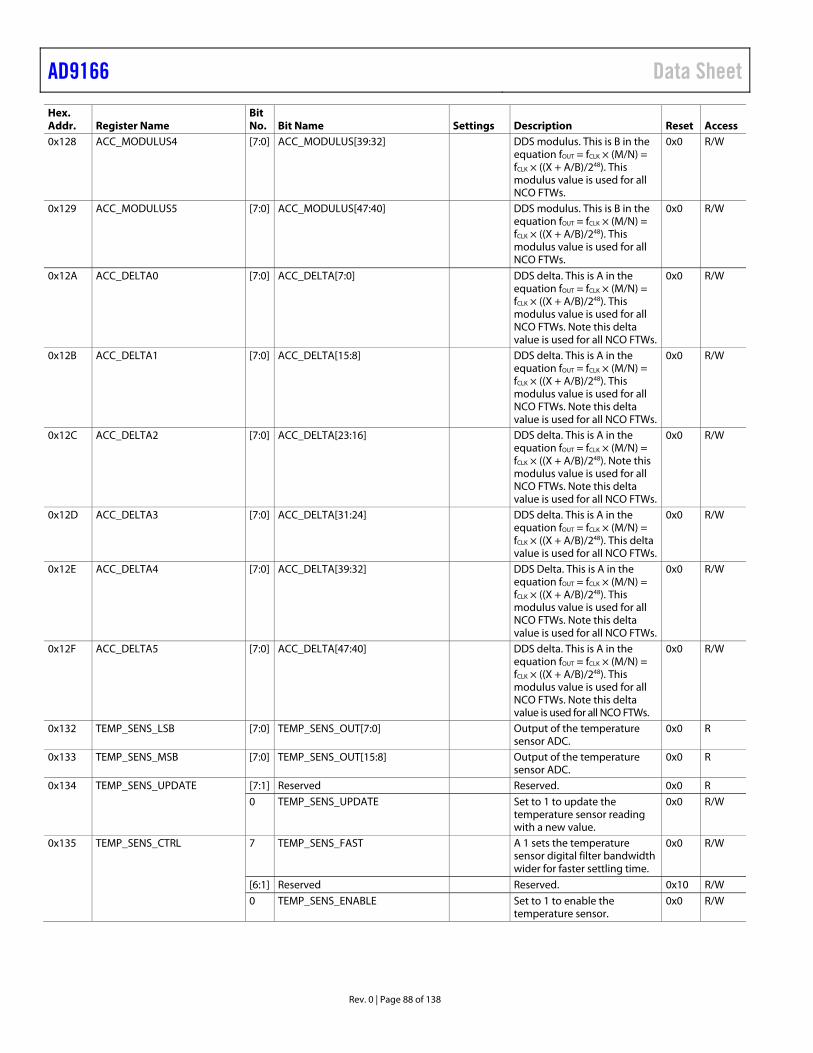
AD9166 Data Sheet
Rev. 0 | Page 88 of 138
Hex. Addr. Register Name
Bit No. Bit Name Settings Description Reset Access
0x128 ACC_MODULUS4 [7:0] ACC_MODULUS[39:32] DDS modulus. This is B in the equation fOUT = fCLK × (M/N) = fCLK × ((X + A/B)/248). This modulus value is used for all NCO FTWs.
0x0 R/W
0x129 ACC_MODULUS5 [7:0] ACC_MODULUS[47:40] DDS modulus. This is B in the equation fOUT = fCLK × (M/N) = fCLK × ((X + A/B)/248). This modulus value is used for all NCO FTWs.
0x0 R/W
0x12A ACC_DELTA0 [7:0] ACC_DELTA[7:0] DDS delta. This is A in the equation fOUT = fCLK × (M/N) = fCLK × ((X + A/B)/248). This modulus value is used for all NCO FTWs. Note this delta value is used for all NCO FTWs.
0x0 R/W
0x12B ACC_DELTA1 [7:0] ACC_DELTA[15:8] DDS delta. This is A in the equation fOUT = fCLK × (M/N) = fCLK × ((X + A/B)/248). This modulus value is used for all NCO FTWs. Note this delta value is used for all NCO FTWs.
0x0 R/W
0x12C ACC_DELTA2 [7:0] ACC_DELTA[23:16] DDS delta. This is A in the equation fOUT = fCLK × (M/N) = fCLK × ((X + A/B)/248). Note this modulus value is used for all NCO FTWs. Note this delta value is used for all NCO FTWs.
0x0 R/W
0x12D ACC_DELTA3 [7:0] ACC_DELTA[31:24] DDS delta. This is A in the equation fOUT = fCLK × (M/N) = fCLK × ((X + A/B)/248). This delta value is used for all NCO FTWs.
0x0 R/W
0x12E ACC_DELTA4 [7:0] ACC_DELTA[39:32] DDS Delta. This is A in the equation fOUT = fCLK × (M/N) = fCLK × ((X + A/B)/248). This modulus value is used for all NCO FTWs. Note this delta value is used for all NCO FTWs.
0x0 R/W
0x12F ACC_DELTA5 [7:0] ACC_DELTA[47:40] DDS delta. This is A in the equation fOUT = fCLK × (M/N) = fCLK × ((X + A/B)/248). This modulus value is used for all NCO FTWs. Note this delta value is used for all NCO FTWs.
0x0 R/W
0x132 TEMP_SENS_LSB [7:0] TEMP_SENS_OUT[7:0] Output of the temperature sensor ADC.
0x0 R
0x133 TEMP_SENS_MSB [7:0] TEMP_SENS_OUT[15:8] Output of the temperature sensor ADC.
0x0 R
0x134 TEMP_SENS_UPDATE [7:1] Reserved Reserved. 0x0 R
0 TEMP_SENS_UPDATE Set to 1 to update the temperature sensor reading with a new value.
0x0 R/W
0x135 TEMP_SENS_CTRL 7 TEMP_SENS_FAST A 1 sets the temperature sensor digital filter bandwidth wider for faster settling time.
0x0 R/W
[6:1] Reserved Reserved. 0x10 R/W
0 TEMP_SENS_ENABLE Set to 1 to enable the temperature sensor.
0x0 R/W
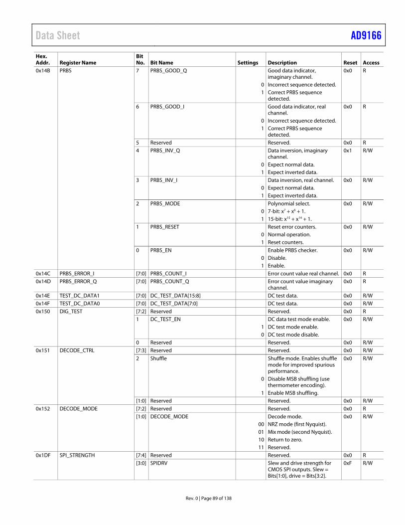
Data Sheet AD9166
Rev. 0 | Page 89 of 138
Hex. Addr. Register Name
Bit No. Bit Name Settings Description Reset Access
0x14B PRBS 7 PRBS_GOOD_Q Good data indicator, imaginary channel.
0x0 R
0 Incorrect sequence detected. 1 Correct PRBS sequence
detected.
6 PRBS_GOOD_I Good data indicator, real channel.
0x0 R
0 Incorrect sequence detected. 1 Correct PRBS sequence
detected.
5 Reserved Reserved. 0x0 R 4 PRBS_INV_Q Data inversion, imaginary
channel. 0x1 R/W
0 Expect normal data. 1 Expect inverted data. 3 PRBS_INV_I Data inversion, real channel. 0x0 R/W 0 Expect normal data. 1 Expect inverted data.
2 PRBS_MODE Polynomial select. 0x0 R/W 0 7-bit: x7 + x6 + 1. 1 15-bit: x15 + x14 + 1. 1 PRBS_RESET Reset error counters. 0x0 R/W 0 Normal operation. 1 Reset counters.
0 PRBS_EN Enable PRBS checker. 0x0 R/W 0 Disable. 1 Enable. 0x14C PRBS_ERROR_I [7:0] PRBS_COUNT_I Error count value real channel. 0x0 R 0x14D PRBS_ERROR_Q [7:0] PRBS_COUNT_Q Error count value imaginary
channel. 0x0 R
0x14E TEST_DC_DATA1 [7:0] DC_TEST_DATA[15:8] DC test data. 0x0 R/W 0x14F TEST_DC_DATA0 [7:0] DC_TEST_DATA[7:0] DC test data. 0x0 R/W 0x150 DIG_TEST [7:2] Reserved Reserved. 0x0 R 1 DC_TEST_EN DC data test mode enable. 0x0 R/W 1 DC test mode enable. 0 DC test mode disable. 0 Reserved Reserved. 0x0 R/W 0x151 DECODE_CTRL [7:3] Reserved Reserved. 0x0 R/W
2 Shuffle Shuffle mode. Enables shuffle mode for improved spurious performance.
0x0 R/W
0 Disable MSB shuffling (use thermometer encoding).
1 Enable MSB shuffling. [1:0] Reserved Reserved. 0x0 R/W 0x152 DECODE_MODE [7:2] Reserved Reserved. 0x0 R [1:0] DECODE_MODE Decode mode. 0x0 R/W 00 NRZ mode (first Nyquist). 01 Mix mode (second Nyquist). 10 Return to zero. 11 Reserved. 0x1DF SPI_STRENGTH [7:4] Reserved Reserved. 0x0 R [3:0] SPIDRV Slew and drive strength for
CMOS SPI outputs. Slew = Bits[1:0], drive = Bits[3:2].
0xF R/W
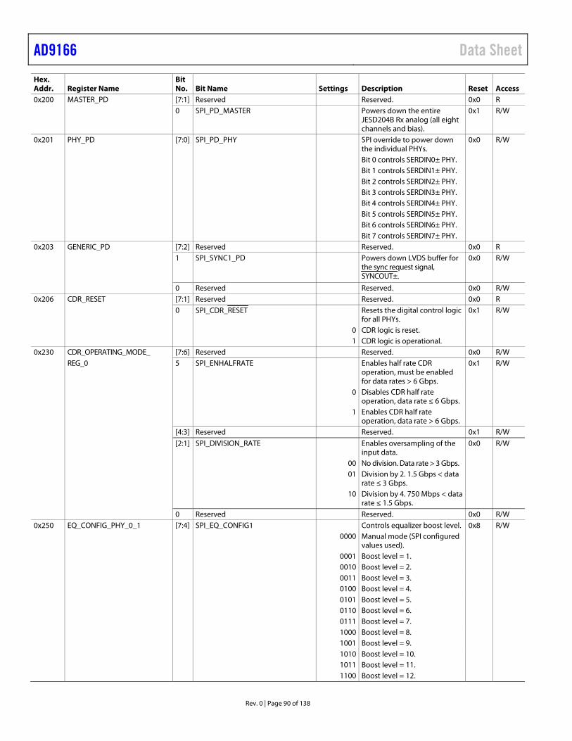
AD9166 Data Sheet
Rev. 0 | Page 90 of 138
Hex. Addr. Register Name
Bit No. Bit Name Settings Description Reset Access
0x200 MASTER_PD [7:1] Reserved Reserved. 0x0 R 0 SPI_PD_MASTER Powers down the entire
JESD204B Rx analog (all eight channels and bias).
0x1 R/W
0x201 PHY_PD [7:0] SPI_PD_PHY SPI override to power down the individual PHYs.
0x0 R/W
Bit 0 controls SERDIN0± PHY. Bit 1 controls SERDIN1± PHY. Bit 2 controls SERDIN2± PHY. Bit 3 controls SERDIN3± PHY. Bit 4 controls SERDIN4± PHY. Bit 5 controls SERDIN5± PHY. Bit 6 controls SERDIN6± PHY. Bit 7 controls SERDIN7± PHY. 0x203 GENERIC_PD [7:2] Reserved Reserved. 0x0 R 1 SPI_SYNC1_PD Powers down LVDS buffer for
the sync request signal, SYNCOUT±.
0x0 R/W
0 Reserved Reserved. 0x0 R/W 0x206 CDR_RESET [7:1] Reserved Reserved. 0x0 R 0 SPI_CDR_RESET Resets the digital control logic
for all PHYs. 0x1 R/W
0 CDR logic is reset. 1 CDR logic is operational. 0x230 CDR_OPERATING_MODE_ [7:6] Reserved Reserved. 0x0 R/W REG_0 5 SPI_ENHALFRATE Enables half rate CDR
operation, must be enabled for data rates > 6 Gbps.
0x1 R/W
0 Disables CDR half rate operation, data rate ≤ 6 Gbps.
1 Enables CDR half rate operation, data rate > 6 Gbps.
[4:3] Reserved Reserved. 0x1 R/W
[2:1] SPI_DIVISION_RATE Enables oversampling of the input data.
0x0 R/W
00 No division. Data rate > 3 Gbps. 01 Division by 2. 1.5 Gbps < data
rate ≤ 3 Gbps.
10 Division by 4. 750 Mbps < data rate ≤ 1.5 Gbps.
0 Reserved Reserved. 0x0 R/W 0x250 EQ_CONFIG_PHY_0_1 [7:4] SPI_EQ_CONFIG1 Controls equalizer boost level. 0x8 R/W 0000 Manual mode (SPI configured
values used).
0001 Boost level = 1. 0010 Boost level = 2. 0011 Boost level = 3. 0100 Boost level = 4. 0101 Boost level = 5. 0110 Boost level = 6. 0111 Boost level = 7. 1000 Boost level = 8. 1001 Boost level = 9. 1010 Boost level = 10. 1011 Boost level = 11. 1100 Boost level = 12.
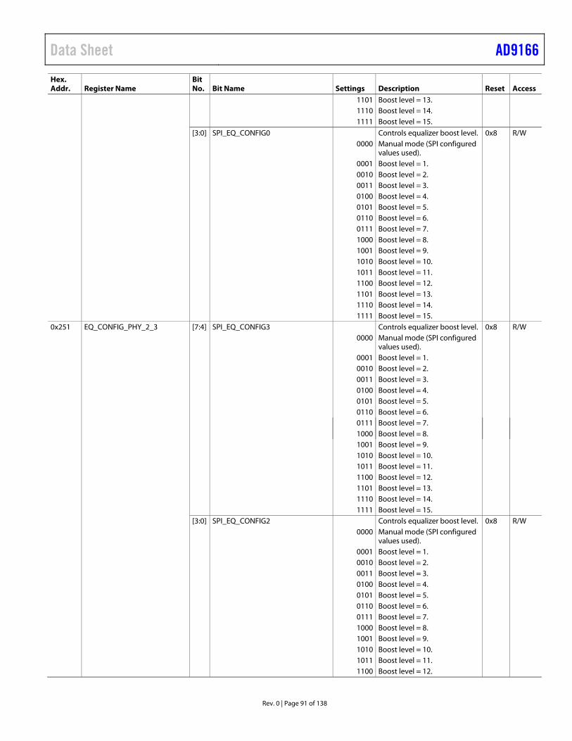
Data Sheet AD9166
Rev. 0 | Page 91 of 138
Hex. Addr. Register Name
Bit No. Bit Name Settings Description Reset Access
1101 Boost level = 13. 1110 Boost level = 14. 1111 Boost level = 15.
[3:0] SPI_EQ_CONFIG0 Controls equalizer boost level. 0x8 R/W 0000 Manual mode (SPI configured
values used).
0001 Boost level = 1. 0010 Boost level = 2. 0011 Boost level = 3. 0100 Boost level = 4. 0101 Boost level = 5. 0110 Boost level = 6. 0111 Boost level = 7. 1000 Boost level = 8. 1001 Boost level = 9. 1010 Boost level = 10. 1011 Boost level = 11. 1100 Boost level = 12. 1101 Boost level = 13. 1110 Boost level = 14. 1111 Boost level = 15. 0x251 EQ_CONFIG_PHY_2_3 [7:4] SPI_EQ_CONFIG3 Controls equalizer boost level. 0x8 R/W 0000 Manual mode (SPI configured
values used).
0001 Boost level = 1. 0010 Boost level = 2. 0011 Boost level = 3. 0100 Boost level = 4. 0101 Boost level = 5. 0110 Boost level = 6. 0111 Boost level = 7. 1000 Boost level = 8. 1001 Boost level = 9. 1010 Boost level = 10. 1011 Boost level = 11. 1100 Boost level = 12. 1101 Boost level = 13. 1110 Boost level = 14. 1111 Boost level = 15. [3:0] SPI_EQ_CONFIG2 Controls equalizer boost level. 0x8 R/W 0000 Manual mode (SPI configured
values used).
0001 Boost level = 1. 0010 Boost level = 2. 0011 Boost level = 3. 0100 Boost level = 4. 0101 Boost level = 5. 0110 Boost level = 6. 0111 Boost level = 7. 1000 Boost level = 8. 1001 Boost level = 9. 1010 Boost level = 10. 1011 Boost level = 11. 1100 Boost level = 12.
AD9166 Data Sheet
Rev. 0 | Page 92 of 138
Hex. Addr. Register Name
Bit No. Bit Name Settings Description Reset Access
1101 Boost Level = 13. 1110 Boost level = 14. 1111 Boost level = 15. 0x252 EQ_CONFIG_PHY_4_5 [7:4] SPI_EQ_CONFIG5 Controls equalizer boost level. 0x8 R/W 0000 Manual mode (SPI configured
values used).
0001 Boost level = 1. 0010 Boost level = 2. 0011 Boost level = 3. 0100 Boost level = 4. 0101 Boost level = 5. 0110 Boost level = 6. 0111 Boost level = 7. 1000 Boost level = 8. 1001 Boost level = 9. 1010 Boost level = 10. 1011 Boost level = 11. 1100 Boost level = 12. 1101 Boost level = 13. 1110 Boost level = 14. 1111 Boost level = 15. [3:0] SPI_EQ_CONFIG4 Controls equalizer boost level. 0x8 R/W 0000 Manual mode (SPI configured
values used).
0001 Boost level = 1. 0010 Boost level = 2. 0011 Boost level = 3. 0100 Boost level = 4. 0101 Boost level = 5. 0110 Boost level = 6. 0111 Boost level = 7. 1000 Boost level = 8. 1001 Boost level = 9. 1010 Boost level = 10. 1011 Boost level = 11. 1100 Boost level = 12. 1101 Boost level = 13. 1110 Boost level = 14. 1111 Boost level = 15. 0x253 EQ_CONFIG_PHY_6_7 [7:4] SPI_EQ_CONFIG7 Controls equalizer boost level. 0x8 R/W 0000 Manual mode (SPI configured
values used).
0001 Boost level = 1. 0010 Boost level = 2. 0011 Boost level = 3. 0100 Boost level = 4. 0101 Boost level = 5. 0110 Boost level = 6. 0111 Boost level = 7. 1000 Boost level = 8. 1001 Boost level = 9. 1010 Boost level = 10. 1011 Boost level = 11. 1100 Boost level = 12.
Data Sheet AD9166
Rev. 0 | Page 93 of 138
Hex. Addr. Register Name
Bit No. Bit Name Settings Description Reset Access
1101 Boost level = 13. 1110 Boost level = 14. 1111 Boost level = 15.
[3:0] SPI_EQ_CONFIG6 Controls equalizer boost level. 0x8 R/W 0000 Manual mode (SPI configured
values used).
0001 Boost level = 1. 0010 Boost level = 2. 0011 Boost level = 3. 0100 Boost level = 4. 0101 Boost level = 5. 0110 Boost level = 6. 0111 Boost level = 7. 1000 Boost level = 8. 1001 Boost level = 9. 1010 Boost level = 10. 1011 Boost level = 11. 1100 Boost level = 12. 1101 Boost level = 13. 1110 Boost level = 14. 1111 Boost level = 15. 0x268 EQ_BIAS_REG [7:6] EQ_POWER_MODE Controls the equalizer power
mode/insertion loss capability. 0x1 R/W
00 Normal mode. 01 Low power mode. [5:0] Reserved Reserved. 0x4 R/W 0x280 SYNTH_ENABLE_CNTRL [7:3] Reserved Reserved. 0x0 R 2 SPI_RECAL_SYNTH Set this bit high to rerun all of
the SERDES PLL calibration routines. Set this bit low again to allow additional recalibra-tions. Rising edge causes the calibration.
0x0 R/W
1 Reserved Reserved. 0x0 R/W 0 SPI_ENABLE_SYNTH Enable the SERDES PLL. Setting
this bit turns on all currents and proceeds to calibrate the PLL. Make sure reference clock and division ratios are correct before enabling this bit.
0x0 R/W
0x281 PLL_STATUS [7:6] Reserved Reserved. 0x0 R 5 SPI_CP_OVER_RANGE_HIGH_RB If set, the SERDES PLL CP
output is above the valid operating range.
0x0 R
0 Charge pump output is within operating range.
1 Charge pump output is above operating range.
4 SPI_CP_OVER_RANGE_LOW_RB If set, the SERDES PLL CP output is below the valid operating range.
0x0 R
0 Charge pump output is within operating range.
1 Charge pump output is below operating range.
AD9166 Data Sheet
Rev. 0 | Page 94 of 138
Hex. Addr. Register Name
Bit No. Bit Name Settings Description Reset Access
3 SPI_CP_CAL_VALID_RB This bit tells the user if the charge pump calibration has completed and is valid.
0x0 R
0 Charge pump calibration is not valid.
1 Charge pump calibration is valid.
[2:1] Reserved Reserved. 0x0 R 0 SPI_PLL_LOCK_RB If set, the SERDES synthesizer
is locked. 0x0 R
0 PLL is not locked. 1 PLL is locked. 0x289 REF_CLK_DIVIDER_LDO [7:2] Reserved Reserved. 0x0 R
[1:0] SERDES_PLL_DIV_FACTOR SERDES PLL reference clock division factor. This field controls the division of the SERDES PLL reference clock before it is fed into the SERDES PLL PFD. It must be set so that fREF/division factor is between 35 MHz and 80 MHz.
0x0 R/W
00 Divide by 4 for lane rate between 6 Gbps and 12.5 Gbps.
01 Divide by 2 for lane rate between 3 Gbps and 6 Gbps.
10 Divide by 1 for lane rate between 1.5 Gbps and 3 Gbps.
0x2A7 TERM_BLK1_CTRLREG0 [7:1] Reserved Reserved. 0x0 R 0 SPI_I_TUNE_R_CAL_TERMBLK1 Rising edge of this bit starts a
termination calibration routine.
0x0 R/W
0x2A8 TERM_BLK1_CTRLREG1 [7:0] SPI_I_SERIALIZER_RTRIM_ TERMBLK1
SPI override for termination value for PHY 0, PHY 1, PHY 6, and PHY 7. Value options are as follows:
0x0 R/W
XXX0XXXX Automatically calibrate termination value.
XXX1000X Force 000 as termination value. XXX1001X Force 001 as termination value. XXX1010X Force 010 as termination value. XXX1011X Force 011 as termination value. XXX1100X Force 100 as termination value. XXX1101X Force 101 as termination value. XXX1110X Force 110 as termination value. XXX1111X Force 111 as termination value. XXX1000X Force 000 as termination value. 0x2AC TERM_BLK1_RD_REG0 [7:4] Reserved Reserved. 0x0 R [3:0] SPI_O_RCAL_CODE_TERMBLK1 Readback of calibration code
for PHY 0, PHY 1, PHY 6, and PHY 7.
0x0 R
0x2AE TERM_BLK2_CTRLREG0 [7:1] Reserved Reserved. 0x0 R 0 SPI_I_TUNE_R_CAL_TERMBLK2 Rising edge of this bit starts a
termination calibration routine.
0x0 R/W
Data Sheet AD9166
Rev. 0 | Page 95 of 138
Hex. Addr. Register Name
Bit No. Bit Name Settings Description Reset Access
0x2AF TERM_BLK2_CTRLREG1 [7:0] SPI_I_SERIALIZER_RTRIM_ TERMBLK2
SPI override for termination value for PHY 2, PHY 3, PHY 4, and PHY 5. Value options are as follows:
0x0 R/W
XXX0XXXX Automatically calibrate termination value.
XXX1000X Force 000 as termination value. XXX1001X Force 001 as termination value. XXX1010X Force 010 as termination value. XXX1011X Force 011 as termination value. XXX1100X Force 100 as termination value. XXX1101X Force 101 as termination value. XXX1110X Force 110 as termination value. XXX1111X Force 111 as termination value. XXX1000X Force 000 as termination value. 0x2B3 TERM_BLK2_RD_REG0 [7:4] Reserved Reserved. 0x0 R [3:0] SPI_O_RCAL_CODE_TERMBLK2 Readback of calibration code
for PHY 2, PHY 3, PHY 4, and PHY 5.
0x0 R
0x2BB TERM_OFFSET_0 [7:4] Reserved Reserved. 0x0 R [3:0] TERM_OFFSET_0 Add or subtract from the
termination calibration value of Physical Lane 0. 4-bit signed magnitude value that adds to or subtracts from the termination value. Bit 3 is the sign bit, and Bits[2:0] are the magnitude bits.
0x0 R/W
0x2BC TERM_OFFSET_1 [7:4] Reserved Reserved. 0x0 R [3:0] TERM_OFFSET_1 Add or subtract from the
termination calibration value of Physical Lane 1. 4-bit signed magnitude value that adds to or subtracts from the termination value. Bit 3 is the sign bit, and Bits[2:0] are the magnitude bits.
0x0 R/W
0x2BD TERM_OFFSET_2 [7:4] Reserved Reserved. 0x0 R [3:0] TERM_OFFSET_2 Add or subtract from the
termination calibration value of Physical Lane 2. 4-bit signed magnitude value that adds to or subtracts from the termination value. Bit 3 is the sign bit, and Bits[2:0] are the magnitude bits.
0x0 R/W
0x2BE TERM_OFFSET_3 [7:4] Reserved Reserved. 0x0 R [3:0] TERM_OFFSET_3 Add or subtract from the
termination calibration value of Physical Lane 3. 4-bit signed magnitude value that adds to or subtracts from the termination value. Bit 3 is the sign bit, and Bits[2:0] are the magnitude bits.
0x0 R/W
AD9166 Data Sheet
Rev. 0 | Page 96 of 138
Hex. Addr. Register Name
Bit No. Bit Name Settings Description Reset Access
0x2BF TERM_OFFSET_4 [7:4] Reserved Reserved. 0x0 R
[3:0] TERM_OFFSET_4 Add or subtract from the termination calibration value of Physical Lane 4. 4-bit signed magnitude value that adds to or subtracts from the termination value. Bit 3 is the sign bit, and Bits[2:0] are the magnitude bits.
0x0 R/W
0x2C0 TERM_OFFSET_5 [7:4] Reserved Reserved. 0x0 R [3:0] TERM_OFFSET_5 Add or subtract from the
termination calibration value of Physical Lane 5. 4-bit signed magnitude value that adds to or subtracts from the termination value. Bit 3 is the sign bit, and Bits[2:0] are the magnitude bits.
0x0 R/W
0x2C1 TERM_OFFSET_6 [7:4] Reserved Reserved. 0x0 R [3:0] TERM_OFFSET_6 Add or subtract from the
termination calibration value of Physical Lane 6. 4-bit signed magnitude value that adds to or subtracts from the termination value. Bit 3 is the sign bit, and Bits[2:0] are the magnitude bits.
0x0 R/W
0x2C2 TERM_OFFSET_7 [7:4] Reserved Reserved. 0x0 R
[3:0] TERM_OFFSET_7 Add or subtract from the termination calibration value of Physical Lane 7. 4-bit signed magnitude value that adds to or subtracts from the termination value. Bit 3 is the sign bit, and Bits[2:0] are the magnitude bits.
0x0 R/W
0x300 GENERAL_JRX_CTRL_0 7 Reserved Reserved. 0x0 R 6 CHECKSUM_MODE JESD204B link parameter
checksum calculation method.0x0 R/W
0 Checksum is sum of fields. 1 Checksum is sum of octets. [5:1] Reserved Reserved. 0x0 R 0 LINK_EN This bit brings up the
JESD204B receiver when all link parameters are programmed and all clocks are ready.
0x0 R/W
0x302 DYN_LINK_LATENCY_0 [7:5] Reserved Reserved. 0x0 R [4:0] DYN_LINK_LATENCY_0 Measurement of the JESD204B
link delay (in PCLK units). Link 0 dynamic link latency. Latency between current deframer LMFC and the global LMFC.
0x0 R
0x304 LMFC_DELAY_0 [7:5] Reserved Reserved. 0x0 R [4:0] LMFC_DELAY_0 Fixed part of the JESD204B
link delay (in PCLK units). Delay in frame clock cycles for global LMFC for Link 0.
0x0 R/W
Data Sheet AD9166
Rev. 0 | Page 97 of 138
Hex. Addr. Register Name
Bit No. Bit Name Settings Description Reset Access
0x306 LMFC_VAR_0 [7:5] Reserved Reserved. 0x0 R [4:0] LMFC_VAR_0 Variable part of the JESD204B
link delay (in PCLK units). Location in Rx LMFC where JESD204B words are read out from buffer. This setting must not be more than 10 PCLKs.
0x1F R/W
0x308 XBAR_LN_0_1 [7:6] Reserved Reserved. 0x0 R
[5:3] SRC_LANE1 Select data from SERDINx±, for Logical Lane 1.
0x1 R/W
000 Data is from SERDIN0±. 001 Data is from SERDIN1±. 010 Data is from SERDIN2±. 011 Data is from SERDIN3±. 100 Data is from SERDIN4±. 101 Data is from SERDIN5±. 110 Data is from SERDIN6±. 111 Data is from SERDIN7±. [2:0] SRC_LANE0 Select data from SERDINx± for
Logical Lane 0. 0x0 R/W
000 Data is from SERDIN0±. 001 Data is from SERDIN1±. 010 Data is from SERDIN2±. 011 Data is from SERDIN3±. 100 Data is from SERDIN4±. 101 Data is from SERDIN5±. 110 Data is from SERDIN6±. 111 Data is from SERDIN7±. 0x309 XBAR_LN_2_3 [7:6] Reserved Reserved. 0x0 R [5:3] SRC_LANE3 Select data from SERDINx± for
Logical Lane 3. 0x3 R/W
000 Data is from SERDIN0±. 001 Data is from SERDIN1±. 010 Data is from SERDIN2±. 011 Data is from SERDIN3±. 100 Data is from SERDIN4±. 101 Data is from SERDIN5±. 110 Data is from SERDIN6±. 111 Data is from SERDIN7±. [2:0] SRC_LANE2 Select data from SERDINx± for
Logical Lane 2. 0x2 R/W
000 Data is from SERDIN0±. 001 Data is from SERDIN1±. 010 Data is from SERDIN2±. 011 Data is from SERDIN3±. 100 Data is from SERDIN4±. 101 Data is from SERDIN5±. 110 Data is from SERDIN6±. 111 Data is from SERDIN7±. 0x30A XBAR_LN_4_5 [7:6] Reserved Reserved. 0x0 R
[5:3] SRC_LANE5 Select data from SERDINx± for Logical Lane 5.
0x5 R/W
000 Data is from SERDIN0±. 001 Data is from SERDIN1±. 010 Data is from SERDIN2±. 011 Data is from SERDIN3±. 100 Data is from SERDIN4±.
AD9166 Data Sheet
Rev. 0 | Page 98 of 138
Hex. Addr. Register Name
Bit No. Bit Name Settings Description Reset Access
101 Data is from SERDIN5±. 110 Data is from SERDIN6±. 111 Data is from SERDIN7±.
[2:0] SRC_LANE4 Select data from SERDINx± for Logical Lane 4.
0x4 R/W
000 Data is from SERDIN0±. 001 Data is from SERDIN1±. 010 Data is from SERDIN2±. 011 Data is from SERDIN3±. 100 Data is from SERDIN4±. 101 Data is from SERDIN5±. 110 Data is from SERDIN6±. 111 Data is from SERDIN7±. 0x30B XBAR_LN_6_7 [7:6] Reserved Reserved. 0x0 R [5:3] SRC_LANE7 Select data from SERDINx± for
Logical Lane 7. 0x7 R/W
000 Data is from SERDIN0±. 001 Data is from SERDIN1±. 010 Data is from SERDIN2±. 011 Data is from SERDIN3±. 100 Data is from SERDIN4±. 101 Data is from SERDIN5±. 110 Data is from SERDIN6±. 111 Data is from SERDIN7±. [2:0] SRC_LANE6 Select data from SERDINx± for
Logical Lane 6. 0x6 R/W
000 Data is from SERDIN0±. 001 Data is from SERDIN1±. 010 Data is from SERDIN2±. 011 Data is from SERDIN3±. 100 Data is from SERDIN4±. 101 Data is from SERDIN5±. 110 Data is from SERDIN6±. 111 Data is from SERDIN7±. 0x30C FIFO_STATUS_REG_0 [7:0] LANE_FIFO_FULL Bit 0 corresponds to FIFO full
flag for data from SERDIN0±. 0x0 R
Bit 1 corresponds to FIFO full flag for data from SERDIN1±.
Bit 2 corresponds to FIFO full flag for data from SERDIN2±.
Bit 3 corresponds to FIFO full flag for data from SERDIN3±.
Bit 4 corresponds to FIFO full flag for data from SERDIN4±.
Bit 5 corresponds to FIFO full flag for data from SERDIN5±.
Bit 6 corresponds to FIFO full flag for data from SERDIN6±.
Bit 7 corresponds to FIFO full flag for data from SERDIN7±.
Data Sheet AD9166
Rev. 0 | Page 99 of 138
Hex. Addr. Register Name
Bit No. Bit Name Settings Description Reset Access
0x30D FIFO_STATUS_REG_1 [7:0] LANE_FIFO_EMPTY Bit 0 corresponds to FIFO empty flag for data from SERDIN0±.
0x0 R
Bit 1 corresponds to FIFO empty flag for data from SERDIN1±.
Bit 2 corresponds to FIFO empty flag for data from SERDIN2±.
Bit 3 corresponds to FIFO empty flag for data from SERDIN3±.
Bit 4 corresponds to FIFO empty flag for data from SERDIN4±.
Bit 5 corresponds to FIFO empty flag for data from SERDIN5±.
Bit 6 corresponds to FIFO empty flag for data from SERDIN6±.
Bit 7 corresponds to FIFO empty flag for data from SERDIN7±.
0x311 SYNC_GEN_0 [7:3] Reserved Reserved. 0x0 R
2 EOMF_MASK_0 Mask end of multiframe (EOMF) flag, based on output from QBD Lane 0. Controls whether SYNCOUT± is asserted in response to loss of multiframe sync.
0x0 R/W
0 Do not assert SYNCOUT± on loss of multiframe.
1 Assert SYNCOUT± on loss of multiframe.
1 Reserved Reserved. 0x0 R/W
0 EOF_MASK_0 Mask end of frame (EOF) flag, based on output from QBD Lane 0. Controls whether SYNCOUT± is asserted in response to loss of frame sync.
0x0 R/W
0 Do not assert SYNCOUT± on loss of frame.
1 Assert SYNCOUT± on loss of frame.
0x312 SYNC_GEN_1 [7:4] SYNC_ERR_DUR Duration of SYNCOUT± signal low for purpose of sync error report. 0 means half PCLK cycle. Add an additional PCLK = 4 octets for each increment of the value.
0x0 R/W
[3:0] SYNC_SYNCREQ_DUR Duration of SYNCOUT± signal low for purpose of sync request. 0 means 5 frames + 9 octets. Add an additional PCLK = 4 octets for each increment of the value.
0x0 R/W
0x313 SYNC_GEN_3 [7:0] LMFC_PERIOD LMFC period in PCLK cycle. This is to report the global LMFC period based on PCLK.
0x0 R
AD9166 Data Sheet
Rev. 0 | Page 100 of 138
Hex. Addr. Register Name
Bit No. Bit Name Settings Description Reset Access
0x315 PHY_PRBS_TEST_EN [7:0] PHY_TEST_EN Enable PHY BER by ungating the clocks.
0x0 R/W
1 PHY test enable. 0 PHY test disable. 0x316 PHY_PRBS_TEST_CTRL 7 Reserved Reserved. 0x0 R
[6:4] PHY_SRC_ERR_CNT 0x0 R/W 000 Report Lane 0 error count. 001 Report Lane 1 error count. 010 Report Lane 2 error count. 011 Report Lane 3 error count. 100 Report Lane 4 error count. 101 Report Lane 5 error count. 110 Report Lane 6 error count. 111 Report Lane 7 error count. [3:2] PHY_PRBS_PAT_SEL Select PRBS pattern for PHY
BER test. 0x0 R/W
00 PRBS7. 01 PRBS15. 10 PRBS31. 11 Not used. 1 PHY_TEST_START Start and stop the PHY PRBS
test. 0x0 R/W
0 Test not started. 1 Test started. 0 PHY_TEST_RESET Reset PHY PRBS test state
machine and error counters. 0x0 R/W
0 Not reset. 1 Reset. 0x317 PHY_PRBS_TEST_
THRESHOLD_LOBITS [7:0] PHY_PRBS_THRESHOLD_LOBITS Bits[7:0] of the 24-bit
threshold value set the error flag for PHY PRBS test.
0x0 R/W
0x318 PHY_PRBS_TEST_ THRESHOLD_MIDBITS
[7:0] PHY_PRBS_THRESHOLD_MIDBITS Bits[15:8] of the 24-bit threshold value set the error flag for PHY PRBS test.
0x0 R/W
0x319 PHY_PRBS_TEST_ THRESHOLD_HIBITS
[7:0] PHY_PRBS_THRESHOLD_HIBITS Bits[23:16] of the 24-bit threshold value set the error flag for PHY PRBS test.
0x0 R/W
0x31A PHY_PRBS_TEST_ERRCNT_ LOBITS
[7:0] PHY_PRBS_ERR_CNT_LOBITS Bits[7:0] of the 24-bit reported PHY BER test error count from selected lane.
0x0 R
0x31B PHY_PRBS_TEST_ERRCNT_ MIDBITS
[7:0] PHY_PRBS_ERR_CNT_MIDBITS Bits[15:8] of the 24-bit reported PHY BER test error count from selected lane.
0x0 R
0x31C PHY_PRBS_TEST_ERRCNT_ HIBITS
[7:0] PHY_PRBS_ERR_CNT_HIBITS Bits[23:16] of the 24-bit reported PHY BER test error count from selected lane.
0x0 R
0x31D PHY_PRBS_TEST_STATUS [7:0] PHY_PRBS_PASS Each bit is for the corresponding lane. Report PHY BER test pass/fail for each lane.
0xFF R
Data Sheet AD9166
Rev. 0 | Page 101 of 138
Hex. Addr. Register Name
Bit No. Bit Name Settings Description Reset Access
0x31E PHY_DATA_SNAPSHOT_CTRL [7:5] Reserved Reserved. 0x0 R [4:2] PHY_GRAB_LANE_SEL Select from which PHY lane to
grab data. 0x0 R/W
000 Grab data from Lane 0. 001 Grab data from Lane 1. 010 Grab data from Lane 2. 011 Grab data from Lane 3. 100 Grab data from Lane 4. 101 Grab data from Lane 5. 110 Grab data from Lane 6. 111 Grab data from Lane 7. 1 PHY_GRAB_MODE Use error trigger to grab data. 0x0 R/W 0 Grab data when
PHY_GRAB_DATA is set.
1 Grab data upon bit error.
0 PHY_GRAB_DATA Transition from 0 to 1 causes logic to store current receive data from one lane.
0x0 R/W
0x31F PHY_SNAPSHOT_DATA_BYTE0 [7:0] PHY_SNAPSHOT_DATA_BYTE0 Stores a single byte, PHY_SNAPSHOT_DATA, Bits[7:0], of a 40-bit snapshot (PHY_SNAPSHOT_DATA, Bits[39:0]) as received on a single PHY lane. The lane to be captured and the capture method is defined in Register 0x31E.
0x0 R
0x320 PHY_SNAPSHOT_DATA_ BYTE1
[7:0] PHY_SNAPSHOT_DATA_BYTE1 Stores a single byte, PHY_SNAPSHOT_DATA, Bits[15:8], of a 40-bit snapshot (PHY_SNAPSHOT_DATA, Bits[39:0]) as received on a single PHY lane. The lane to be captured and the capture method is defined in Register 0x31E.
0x0 R
0x321 PHY_SNAPSHOT_DATA_ BYTE2
[7:0] PHY_SNAPSHOT_DATA_BYTE2 Stores a single byte, PHY_SNAPSHOT_DATA, Bits[23:16], of a 40-bit snapshot (PHY_SNAPSHOT_ DATA, Bits[39:0]) as received on a single PHY lane. The lane to be captured and the capture method is defined in Register 0x31E.
0x0 R
0x322 PHY_SNAPSHOT_DATA_ BYTE3
[7:0] PHY_SNAPSHOT_DATA_BYTE3 Stores a single byte, PHY_SNAPSHOT_DATA, Bits[31:24], of a 40-bit snapshot (PHY_SNAPSHOT_ DATA, Bits[39:0]) as received on a single PHY lane. The lane to be captured and the capture method is defined in Register 0x31E.
0x0 R
0x323 PHY_SNAPSHOT_DATA_ BYTE4
[7:0] PHY_SNAPSHOT_DATA_BYTE4 Stores a single byte, PHY_SNAPSHOT_DATA, Bits[39:32], of a 40-bit snapshot (PHY_SNAPSHOT_ DATA, Bits[39:0]) as received on a single PHY lane. The lane to be captured and the capture method is defined in Register 0x31E.
0x0 R
AD9166 Data Sheet
Rev. 0 | Page 102 of 138
Hex. Addr. Register Name
Bit No. Bit Name Settings Description Reset Access
0x32C SHORT_TPL_TEST_0 [7:4] SHORT_TPL_SP_SEL Short transport layer sample selection. Select which sample to check from a specific DAC.
0x0 R/W
0000 Sample 0. 0001 Sample 1. 0010 Sample 2. 0011 Sample 3. 0100 Sample 4. 0101 Sample 5. 0110 Sample 6. 0111 Sample 7. 1000 Sample 8. 1001 Sample 9. 1010 Sample 10. 1011 Sample 11. 1100 Sample 12. 1101 Sample 13. 1110 Sample 14. 1111 Sample 15.
[3:2] SHORT_TPL_M_SEL Short transport layer test DAC selection. Select which DAC to check.
0x0 R/W
00 DAC 0. 01 DAC 1. 10 DAC 2. 11 DAC 3. 1 SHORT_TPL_TEST_RESET Short transport layer test
reset. Resets the result of short transport layer test.
0x0 R/W
0 Not reset. 1 Reset. 0 SHORT_TPL_TEST_EN Short transport layer test
enable. Enable short transport layer test.
0x0 R/W
0 Disable. 1 Enable. 0x32D SHORT_TPL_TEST_1 [7:0] SHORT_TPL_REF_SP_LSB Short transport layer reference
sample LSB. This LSB is the lower eight bits of expected DAC sample, and is used to compare with the received DAC sample at the output of JESD204B Rx.
0x0 R/W
0x32E SHORT_TPL_TEST_2 [7:0] SHORT_TPL_REF_SP_MSB Short transport layer test reference sample MSB. This LSB is the upper eight bits of expected DAC sample, and is used to compare with the received sample at JESD204B Rx output.
0x0 R/W
0x32F SHORT_TPL_TEST_3 [7:1] Reserved Reserved. 0x0 R
0 SHORT_TPL_FAIL Short transport layer test fail. This bit shows if the selected DAC sample matches the reference sample. If they match, the test passes. Otherwise, the test fails.
0x0 R
0 Test pass. 1 Test fail.
Data Sheet AD9166
Rev. 0 | Page 103 of 138
Hex. Addr. Register Name
Bit No. Bit Name Settings Description Reset Access
0x334 JESD_BIT_INVERSE_CTRL [7:0] JESD_BIT_INVERSE Each bit of this byte inverses the JESD204B deserialized data from one specific JESD204B Rx PHY. The bit order matches the logical lane order. For example, Bit 0 controls Lane 0, Bit 1 controls Lane 1.
0x0 R/W
0x400 DID_REG [7:0] DID_RD Received ILAS configuration on Lane 0. DID is the device ID number. Link information received on Lane 0 as specified in Section 8.3 of JESD204B.
0x0 R
0x401 BID_REG [7:0] BID_RD Received ILAS configuration on Lane 0. BID is the bank ID, extension to DID. Link information received on Lane 0 as specified in Section 8.3 of JESD204B.
0x0 R
0x402 LID0_REG 7 Reserved Reserved. 0x0 R 6 ADJDIR_RD Received ILAS configuration
on Lane 0. ADJDIR is the direction to adjust the DAC LMFC. Link information received on Lane 0 as specified in Section 8.3 of JESD204B.
0x0 R
5 PHADJ_RD Received ILAS configuration on Lane 0. PHADJ is the phase adjustment request to DAC. Link information received on Lane 0 as specified in Section 8.3 of JESD204B.
0x0 R
[4:0] LL_LID0 Received ILAS LID configuration on Lane 0. LID0 is the lane identification for Lane 0. Link information received on Lane 0 as specified in Section 8.3 of JESD204B.
0x0 R
0x403 SCR_L_REG 7 SCR_RD Received ILAS configuration on Lane 0. SCR is the Tx scrambling status. Link information received on Lane 0 as specified in Section 8.3 of JESD204B.
0x0 R
0 Scrambling is disabled. 1 Scrambling is enabled.
[6:5] Reserved Reserved. 0x0 R [4:0] L_RD Received ILAS configuration
on Lane 0. L is the number of lanes per converter device. Link information received on Lane 0 as specified in Section 8.3 of JESD204B.
0x0 R
00000 1 lane per converter device. 00001 2 lanes per converter device. 00011 4 lanes per converter device. 00111 8 lanes per converter device.
AD9166 Data Sheet
Rev. 0 | Page 104 of 138
Hex. Addr. Register Name
Bit No. Bit Name Settings Description Reset Access
0x404 F_REG [7:0] F_RD Received ILAS configuration on Lane 0. F is the number of octets per frame. Settings of 1, 2, and 4 are valid (value in register is F − 1). Link infor-mation received on Lane 0 as specified in Section 8.3 of JESD204B.
0x0 R
0 1 octet per frame. 1 2 octets per frame. 11 4 octets per frame. 0x405 K_REG [7:5] Reserved Reserved. 0x0 R [4:0] K_RD Received ILAS configuration
on Lane 0. K is the number of frames per multiframe. Settings of 16 or 32 are valid. On this device, all modes use K = 32 (value in register is K − 1). Link information received on Lane 0 as specified in Section 8.3 of JESD204B.
0x0 R
01111 16 frames per multiframe. 11111 32 frames per multiframe. 0x406 M_REG [7:0] M_RD Received ILAS configuration
on Lane 0. M is the number of converters per device. Link information received on Lane 0 as specified in Section 8.3 of JESD204B. M is 1 for real interface and 2 for complex interface (value in register is M − 1).
0x0 R
0x407 CS_N_REG [7:6] CS_RD Received ILAS configuration on Lane 0. CS is the number of control bits per sample. Link information received on Lane 0 as specified in Section 8.3 of JESD204B. CS is always 0 on this device.
0x0 R
5 Reserved Reserved. 0x0 R [4:0] N_RD Received ILAS configuration
on Lane 0. N is the converter resolution. Value in register is N − 1 (for example, 16 bits = 0b01111).
0x0 R
0x408 NP_REG [7:5] SUBCLASSV_RD Received ILAS configuration on Lane 0. SUBCLASSV is the device subclass version. Link information received on Lane 0 as specified in Section 8.3 of JESD204B.
0x0 R
000 Subclass 0. 001 Subclass 1.
[4:0] NP_RD Received ILAS configuration on Lane 0. NP is the total number of bits per sample. Link information received on Lane 0 as specified in Section 8.3 of JESD204B. Value in register is NP − 1, for example, 16 bits per sample = 0b01111.
0x0 R
Data Sheet AD9166
Rev. 0 | Page 105 of 138
Hex. Addr. Register Name
Bit No. Bit Name Settings Description Reset Access
0x409 S_REG [7:5] JESDV_RD Received ILAS configuration on Lane 0. JESDV is the JESD204x version. Link information received on Lane 0 as specified in Section 8.3 of JESD204B.
0x0 R
000 JESD204A. 001 JESD204B. [4:0] S_RD Received ILAS configuration
on Lane 0. S is the number of samples per converter per frame cycle. Link information received on Lane 0 as specified in Section 8.3 of JESD204B. Value in register is S − 1.
0x0 R
0x40A HD_CF_REG 7 HD_RD Received ILAS configuration on Lane 0. HD is the high density format. Refer to Section 5.1.3 of JESD204B standard. Link information received on Lane 0 as specified in Section 8.3 of JESD204B.
0x0 R
0 Low density mode. 1 High density mode. [6:5] Reserved Reserved. 0x0 R [4:0] CF_RD Received ILAS configuration
on Lane 0. CF is the number of control words per frame clock period per link. Link information received on Lane 0 as specified in Section 8.3 of JESD204B. CF is always 0 on this device.
0x0 R
0x40B RES1_REG [7:0] RES1_RD Received ILAS configuration on Lane 0. Reserved Field 1. Link information received on Lane 0 as specified in Section 8.3 of JESD204B.
0x0 R
0x40C RES2_REG [7:0] RES2_RD Received ILAS configuration on Lane 0. Reserved Field 2. Link information received on Lane 0 as specified in Section 8.3 of JESD204B.
0x0 R
0x40D CHECKSUM0_REG [7:0] LL_FCHK0 Received checksum during ILAS on Lane 0. Checksum for Lane 0. Link information received on Lane 0 as specified in Section 8.3 of JESD204B.
0x0 R
0x40E COMPSUM0_REG [7:0] LL_FCMP0 Computed checksum on Lane 0. Computed checksum for Lane 0. The JESD204B Rx computes the checksum of the link information received on Lane 0 as specified in Section 8.3 of JESD204B. The computation method is set by the CHECKSUM_MODE bit (Register 0x300, Bit 6) and must match the likewise calculated checksum in Register 0x40D.
0x0 R
AD9166 Data Sheet
Rev. 0 | Page 106 of 138
Hex. Addr. Register Name
Bit No. Bit Name Settings Description Reset Access
0x412 LID1_REG [7:5] Reserved Reserved. 0x0 R [4:0] LL_LID1 Received lane ID (LID) during
ILAS on Lane 1. Link information received on Lane 0 as specified in Section 8.3 of JESD204B.
0x0 R
0x415 CHECKSUM1_REG [7:0] LL_FCHK1 Received checksum during ILAS on Lane 1. Link information received on Lane 0 as specified in Section 8.3 of JESD204B.
0x0 R
0x416 COMPSUM1_REG [7:0] LL_FCMP1 Computed checksum on Lane 1 (see description for Register 0x40E).
0x0 R
0x41A LID2_REG [7:5] Reserved Reserved. 0x0 R [4:0] LL_LID2 Received lane ID (LID) during
ILAS on Lane 2. 0x0 R
0x41D CHECKSUM2_REG [7:0] LL_FCHK2 Received checksum during ILAS on Lane 2
0x0 R
0x41E COMPSUM2_REG [7:0] LL_FCMP2 Computed checksum on Lane 2 (see description for Register 0x40E).
0x0 R
0x422 LID3_REG [7:5] Reserved Reserved. 0x0 R [4:0] LL_LID3 Received lane ID (LID) during
ILAS on Lane 3. 0x0 R
0x425 CHECKSUM3_REG [7:0] LL_FCHK3 Received checksum during ILAS on Lane 3
0x0 R
0x426 COMPSUM3_REG [7:0] LL_FCMP3 Computed checksum on Lane 3 (see description for Register 0x40E).
0x0 R
0x42A LID4_REG [7:5] Reserved Reserved. 0x0 R [4:0] LL_LID4 Received LID during ILAS on
Lane 4. 0x0 R
0x42D CHECKSUM4_REG [7:0] LL_FCHK4 Received checksum during ILAS on Lane 4
0x0 R
0x42E COMPSUM4_REG [7:0] LL_FCMP4 Computed checksum on Lane 4 (see description for Register 0x40E).
0x0 R
0x432 LID5_REG [7:5] Reserved Reserved. 0x0 R [4:0] LL_LID5 Received LID during ILAS on
Lane 5. 0x0 R
0x435 CHECKSUM5_REG [7:0] LL_FCHK5 Received checksum during ILAS on Lane 5
0x0 R
0x436 COMPSUM5_REG [7:0] LL_FCMP5 Computed checksum on Lane 5 (see description for Register 0x40E).
0x0 R
0x43A LID6_REG [7:5] Reserved Reserved. 0x0 R [4:0] LL_LID6 Received LID during ILAS on
Lane 6. 0x0 R
0x43D CHECKSUM6_REG [7:0] LL_FCHK6 Received checksum during ILAS on Lane 6
0x0 R
0x43E COMPSUM6_REG [7:0] LL_FCMP6 Computed checksum on Lane 6 (see description for Register 0x40E).
0x0 R
0x442 LID7_REG [7:5] Reserved Reserved. 0x0 R [4:0] LL_LID7 Received LID during ILAS on
Lane 7. 0x0 R
0x445 CHECKSUM7_REG [7:0] LL_FCHK7 Received checksum during ILAS on Lane 7.
0x0 R
0x446 COMPSUM7_REG [7:0] LL_FCMP7 Computed checksum on Lane 7 (see description for Register 0x40E).
0x0 R
Data Sheet AD9166
Rev. 0 | Page 107 of 138
Hex. Addr. Register Name
Bit No. Bit Name Settings Description Reset Access
0x450 ILS_DID [7:0] DID Device (link) identification number (DID). DID is the device ID number. Link information received on Lane 0 as specified in Section 8.3 of JESD204B. Must be set to the value read in Register 0x400. This signal must only be programmed while the QBD is held in soft reset (Register 0x475, Bit 3), and must not be changed during normal operation.
0x0 R/W
0x451 ILS_BID [7:0] BID Bank ID, extension to DID. This signal must only be pro-grammed while the QBD is held in soft reset (Register 0x475, Bit 3), and must not be changed during normal operation.
0x0 R/W
0x452 ILS_LID0 7 Reserved Reserved. 0x0 R 6 ADJDIR Direction to adjust DAC LMFC
(Subclass 2 only). ADJDIR is the direction to adjust DAC LMFC. Link information received on Lane 0 as specified in Section 8.3 of JESD204B. This signal must only be pro-grammed while the QBD is held in soft reset (Register 0x475, Bit 3), and must not be changed during normal operation.
0x0 R/W
5 PHADJ Phase adjustment to DAC (Subclass 2 only). PHADJ is the phase adjustment request to the DAC. Link information received on Lane 0 as specified in Section 8.3 of JESD204B. This signal must only be pro-grammed while the QBD is held in soft reset (Register 0x475, Bit 3), and must not be changed during normal operation.
0x0 R/W
[4:0] LID0 Lane identification number (within link). LID0 is the lane identification for Lane 0. Link information received on Lane 0 as specified in Section 8.3 of JESD204B. This signal must only be programmed while the QBD is held in soft reset (Register 0x475, Bit 3), and must not be changed during normal operation.
0x0 R/W
0x453 ILS_SCR_L 7 SCR Scramble enable. SCR is the Rx descrambling enable. This signal must only be pro-grammed while the QBD is held in soft reset (Register 0x475, Bit 3), and must not be changed during normal operation.
0x1 R/W
0 Descrambling is disabled. 1 Descrambling is enabled.
AD9166 Data Sheet
Rev. 0 | Page 108 of 138
Hex. Addr. Register Name
Bit No. Bit Name Settings Description Reset Access
[6:5] Reserved Reserved. 0x0 R [4:0] L Number of lanes per converter
(minus 1). L is the number of lanes per converter device. Settings of 1, 2, 3, 4, 6, and 8 are valid. Refer to Table 15 and Table 16.
0x7 R
0x454 ILS_F [7:0] F Number of octets per frame (minus 1). This value of F is not used to soft configure the QBD. Register CTRLREG1 is used to soft configure the QBD.
0x0 R
0x455 ILS_K [7:5] Reserved Reserved. 0x0 R [4:0] K Number of frames per
multiframe (minus 1). K is the number of frames per multiframe. On this device, all modes use K = 32 (value in register is K − 1). This signal must only be programmed while the QBD is held in soft reset (Register 0x475, Bit 3), and must not be changed during normal operation.
0x1F R/W
01111 16 frames per multiframe. 11111 32 frames per multiframe. 0x456 ILS_M [7:0] M Number of converters per
device (minus 1). M is the number of converters/device. Settings of 1 and 2 are valid. Refer to Table 15 and Table 16.
0x1 R
0x457 ILS_CS_N [7:6] CS Number of control bits per sample. CS is the number of control bits per sample. Must be set to 0. Control bits are not supported.
0x0 R
5 Reserved Reserved. 0x0 R [4:0] N Converter resolution (minus 1).
N is the converter resolution. Must be set to 16 (0x0F).
0xF R
0x458 ILS_NP [7:5] SUBCLASSV Device subclass version. SUBCLASSV is the device subclass version. This signal must only be programmed while the QBD is held in soft reset (Register 0x475, Bit 3), and must not be changed during normal operation.
0x0 R/W
000 Subclass 0. 001 Subclass 1. 010 Subclass 2 (not supported). [4:0] NP Total number of bits per
sample (minus 1). NP is the total number of bits per sample. Must be set to 16 (0x0F). Refer to Table 15 and Table 16.
0xF R
Data Sheet AD9166
Rev. 0 | Page 109 of 138
Hex. Addr. Register Name
Bit No. Bit Name Settings Description Reset Access
0x459 ILS_S [7:5] JESDV JESD204x version. JESDV is the JESD204x version. This signal must only be programmed while the QBD is held in soft reset (Register 0x475, Bit 3), and must not be changed during normal operation.
0x0 R/W
000 JESD204A. 001 JESD204B.
[4:0] S Number of samples per converter per frame cycle (minus 1). S is the number of samples per converter per frame cycle. Settings of 1 and 2 are valid. Refer to Table 15 and Table 16.
0x1 R
0x45A ILS_HD_CF 7 HD High density format. HD is the high density mode. Refer to Section 5.1.3 of JESD204B standard.
0x1 R
0 Low density mode. 1 High density mode. [6:5] Reserved Reserved. 0x0 R [4:0] CF Number of control bits per
sample. CF is the number of control words per frame clock period per link. Must be set to 0. Control bits are not supported.
0x0 R
0x45B ILS_RES1 [7:0] RES1 Reserved. Reserved Field 1. This signal must only be programmed while the QBD is held in soft reset (Register 0x475, Bit 3), and must not be changed during normal operation.
0x0 R/W
0x45C ILS_RES2 [7:0] RES2 Reserved. Reserved Field 2. This signal must only be programmed while the QBD is held in soft reset (Register 0x475, Bit 3), and must not be changed during normal operation.
0x0 R/W
0x45D ILS_CHECKSUM [7:0] FCHK0 Link configuration checksum. Checksum for Lane 0. The checksum for the values programmed into Register 0x450 to Register 0x45C must be calculated according to Section 8.3 of the JESD204B specification and written to this register (SUM(Register 0x450 to Register 0x45C) % 256). This signal must only be programmed while the QBD is held in soft reset (Register 0x475, Bit 3), and must not be changed during normal operation.
0x0 R/W
AD9166 Data Sheet
Rev. 0 | Page 110 of 138
Hex. Addr. Register Name
Bit No. Bit Name Settings Description Reset Access
0x46C LANE_DESKEW 7 ILD7 Interlane deskew status for Lane 7 (ignore this output when NO_ILAS = 1).
0x0 R
0 Deskew failed. 1 Deskew achieved.
6 ILS6 Initial lane synchronization status for Lane 6 (ignore this output when NO_ILAS = 1).
0x0 R
0 Synchronization lost. 1 Synchronization achieved.
5 ILD5 Interlane deskew status for Lane 5 (ignore this output when NO_ILAS = 1).
0x0 R
0 Deskew failed. 1 Deskew achieved.
4 ILD4 Interlane deskew status for Lane 4 (ignore this output when NO_ILAS = 1).
0x0 R
0 Deskew failed. 1 Deskew achieved. 3 ILD3 Interlane deskew status for
Lane 3 (ignore this output when NO_ILAS = 1).
0x0 R
0 Deskew failed. 1 Deskew achieved. 2 ILD2 Interlane deskew status for
Lane 2 (ignore this output when NO_ILAS = 1).
0x0 R
0 Deskew failed. 1 Deskew achieved. 1 ILD1 Interlane deskew status for
Lane 1 (ignore this output when NO_ILAS = 1).
0x0 R
0 Deskew failed. 1 Deskew achieved. 0 ILD0 Interlane deskew status for
Lane 0 (ignore this output when NO_ILAS = 1).
0x0 R
0 Deskew failed. 1 Deskew achieved. 0x46D BAD_DISPARITY 7 BDE7 BDE status for Lane 7. 0x0 R 0 Error count < ETH[7:0] value. 1 Error count ≥ ETH[7:0] value.
6 BDE6 BDE status for Lane 6. 0x0 R 0 Error count < ETH[7:0] value. 1 Error count ≥ ETH[7:0] value. 5 BDE5 BDE status for Lane 5. 0x0 R 0 Error count < ETH[7:0] value. 1 Error count ≥ ETH[7:0] value. 4 BDE4 BDE status for Lane 4. 0x0 R 0 Error count < ETH[7:0] value. 1 Error count ≥ ETH[7:0] value. 3 BDE3 BDE status for Lane 3. 0x0 R 0 Error count < ETH[7:0] value. 1 Error count ≥ ETH[7:0] value.
Data Sheet AD9166
Rev. 0 | Page 111 of 138
Hex. Addr. Register Name
Bit No. Bit Name Settings Description Reset Access
2 BDE2 BDE status for Lane 2. 0x0 R 0 Error count < ETH[7:0] value. 1 Error count ≥ ETH[7:0] value. 1 BDE1 BDE status for Lane 1. 0x0 R 0 Error count < ETH[7:0] value. 1 Error count ≥ ETH[7:0] value.
0 BDE0 BDE status for Lane 0. 0x0 R 0 Error count < ETH[7:0] value. 1 Error count ≥ ETH[7:0] value. 0x46E NOT_IN_TABLE 7 NIT7 NIT error status for Lane 7. 0x0 R 0 Error count < ETH[7:0] value. 1 Error count ≥ ETH[7:0] value.
6 NIT6 NIT error status for Lane 6. 0x0 R 0 Error count < ETH[7:0] value. 1 Error count ≥ ETH[7:0] value.
5 NIT5 NIT errors status for Lane 5. 0x0 R 0 Error count < ETH[7:0] value. 1 Error count ≥ ETH[7:0] value.
4 NIT4 NIT error status for Lane 4. 0x0 R 0 Error count < ETH[7:0] value. 1 Error count ≥ ETH[7:0] value. 3 NIT3 NIT error status for Lane 3. 0x0 R 0 Error count < ETH[7:0] value. 1 Error count ≥ ETH[7:0] value. 2 NIT2 NIT error status for Lane 2. 0x0 R 0 Error count < ETH[7:0] value. 1 Error count ≥ ETH[7:0] value. 1 NIT1 NIT error status for Lane 1. 0x0 R 0 Error count < ETH[7:0] value. 1 Error count ≥ ETH[7:0] value.
0 NIT0 NIT error status for Lane 0. 0x0 R 0 Error count < ETH[7:0] value. 1 Error count ≥ ETH[7:0] value. 0x46F UNEXPECTED_KCHAR 7 UEK7 UEK character error status for
Lane 7. 0x0 R
0 Error count < ETH[7:0] value. 1 Error count ≥ ETH[7:0] value. 6 UEK6 UEK character error status for
Lane 6. 0x0 R
0 Error count < ETH[7:0] value. 1 Error count ≥ ETH[7:0] value.
5 UEK5 UEK character error status for Lane 5.
0x0 R
0 Error count < ETH[7:0] value. 1 Error count ≥ ETH[7:0] value. 4 UEK4 UEK character error status for
Lane 4. 0x0 R
0 Error count < ETH[7:0] value. 1 Error count ≥ ETH[7:0] value. 3 UEK3 UEK character error status for
Lane 3. 0x0 R
0 Error count < ETH[7:0] value. 1 Error count ≥ ETH[7:0] value.
AD9166 Data Sheet
Rev. 0 | Page 112 of 138
Hex. Addr. Register Name
Bit No. Bit Name Settings Description Reset Access
2 UEK2 UEK character error status for Lane 2.
0x0 R
0 Error count < ETH[7:0] value. 1 Error count ≥ ETH[7:0] value. 1 UEK1 UEK character error status for
Lane 1. 0x0 R
0 Error count < ETH[7:0] value. 1 Error count ≥ ETH[7:0] value. 0 UEK0 UEK character error status for
Lane 0. 0x0 R
0 Error count < ETH[7:0] value. 1 Error count ≥ ETH[7:0] value. 0x470 CODE_GRP_SYNC 7 CGS7 CGS status for Lane 7. 0x0 R 0 Synchronization lost. 1 Synchronization achieved.
6 CGS6 CGS status for Lane 6. 0x0 R 0 Synchronization lost. 1 Synchronization achieved. 5 CGS5 CGS status for Lane 5. 0x0 R 0 Synchronization lost. 1 Synchronization achieved. 4 CGS4 CGS status for Lane 4. 0x0 R 0 Synchronization lost. 1 Synchronization achieved. 3 CGS3 CGS status for Lane 3. 0x0 R 0 Synchronization lost. 1 Synchronization achieved.
2 CGS2 CGS status for Lane 2. 0x0 R 0 Synchronization lost. 1 Synchronization achieved. 1 CGS1 CGS status for Lane 1. 0x0 R 0 Synchronization lost. 1 Synchronization achieved.
0 CGS0 CGS status for Lane 0. 0x0 R 0 Synchronization lost. 1 Synchronization achieved. 0x471 FRAME_SYNC 7 FS7 Frame sync status for Lane 7
(ignore this output when NO_ILAS = 1).
0x0 R
0 Synchronization lost. 1 Synchronization achieved. 6 FS6 Frame sync status for Lane 6
(ignore this output when NO_ILAS = 1).
0x0 R
0 Synchronization lost. 1 Synchronization achieved.
5 FS5 Frame sync status for Lane 5 (ignore this output when NO_ILAS = 1).
0x0 R
0 Synchronization lost. 1 Synchronization achieved. 4 FS4 Frame sync status for Lane 4
(ignore this output when NO_ILAS = 1).
0x0 R
0 Synchronization lost. 1 Synchronization achieved.
Data Sheet AD9166
Rev. 0 | Page 113 of 138
Hex. Addr. Register Name
Bit No. Bit Name Settings Description Reset Access
3 FS3 Frame sync status for Lane 3 (ignore this output when NO_ILAS = 1).
0x0 R
0 Synchronization lost. 1 Synchronization achieved. 2 FS2 Frame sync status for Lane 2
(ignore this output when NO_ILAS = 1).
0x0 R
0 Synchronization lost. 1 Synchronization achieved.
1 FS1 Frame sync status for Lane 1 (ignore this output when NO_ILAS = 1).
0x0 R
0 Synchronization lost. 1 Synchronization achieved. 0 FS0 Frame sync status for Lane 0
(ignore this output when NO_ILAS = 1).
0x0 R
0 Synchronization lost. 1 Synchronization achieved. 0x472 GOOD_CHECKSUM 7 CKS7 Computed checksum status
for Lane 7 (ignore this output when NO_ILAS = 1).
0x0 R
0 Checksum is incorrect. 1 Checksum is correct.
6 CKS6 Computed checksum status for Lane 6 (ignore this output when NO_ILAS = 1).
0x0 R
0 Checksum is incorrect. 1 Checksum is correct.
5 CKS5 Computed checksum status for Lane 5 (ignore this output when NO_ILAS = 1).
0x0 R
0 Checksum is incorrect. 1 Checksum is correct. 4 CKS4 Computed checksum status
for Lane 4 (ignore this output when NO_ILAS = 1).
0x0 R
0 Checksum is incorrect. 1 Checksum is correct. 3 CKS3 Computed checksum status
for Lane 3 (ignore this output when NO_ILAS = 1).
0x0 R
0 Checksum is incorrect. 1 Checksum is correct.
2 CKS2 Computed checksum status for Lane 2 (ignore this output when NO_ILAS = 1).
0x0 R
0 Checksum is incorrect. 1 Checksum is correct. 1 CKS1 Computed checksum status
for Lane 1 (ignore this output when NO_ILAS = 1).
0x0 R
0 Checksum is incorrect. 1 Checksum is correct.
AD9166 Data Sheet
Rev. 0 | Page 114 of 138
Hex. Addr. Register Name
Bit No. Bit Name Settings Description Reset Access
0 CKS0 Computed checksum status for Lane 0 (ignore this output when NO_ILAS = 1).
0x0 R
0 Checksum is incorrect. 1 Checksum is correct. 0x473 INIT_LANE_SYNC 7 ILS7 Initial lane synchronization
status for Lane 7 (ignore this output when NO_ILAS = 1).
0x0 R
0 Synchronization lost. 1 Synchronization achieved.
6 ILS6 Initial lane synchronization status for Lane 6 (ignore this output when NO_ILAS = 1).
0x0 R
0 Synchronization lost. 1 Synchronization achieved. 5 ILS5 Initial lane synchronization
status for Lane 5 (ignore this output when NO_ILAS = 1).
0x0 R
0 Synchronization lost. 1 Synchronization achieved. 4 ILS4 Initial lane synchronization
status for Lane 4 (ignore this output when NO_ILAS = 1).
0x0 R
0 Synchronization lost. 1 Synchronization achieved.
3 ILS3 Initial lane synchronization status for Lane 3 (ignore this output when NO_ILAS = 1).
0x0 R
0 Synchronization lost. 1 Synchronization achieved.
2 ILS2 Initial lane synchronization status for Lane 2 (ignore this output when NO_ILAS = 1).
0x0 R
0 Synchronization lost. 1 Synchronization achieved. 1 ILS1 Initial lane synchronization
status for Lane 1 (ignore this output when NO_ILAS = 1).
0x0 R
0 Synchronization lost. 1 Synchronization achieved. 0 ILS0 Initial lane synchronization
status for Lane 0 (ignore this output when NO_ILAS = 1).
0x0 R
0 Synchronization lost. 1 Synchronization achieved. 0x475 CTRLREG0 7 RX_DIS Level input: disable deframer
receiver when this input = 1. This signal must only be pro-grammed while the QBD is held in soft reset (Register 0x475, Bit 3), and must not be changed during normal operation.
0x0 R/W
1 Disable character replacement of /A/ and /F/ control characters at the end of received frames and multiframes.
0 Enables the substitution.
Data Sheet AD9166
Rev. 0 | Page 115 of 138
Hex. Addr. Register Name
Bit No. Bit Name Settings Description Reset Access
6 CHAR_REPL_DIS When this input = 1, character replacement at the end of frame/multiframe is disabled. This signal must only be pro-grammed while the QBD is held in soft reset (Register 0x475, Bit 3), and must not be changed during normal operation.
0x0 R/W
[5:4] Reserved Reserved. 0x0 R
3 SOFTRST Soft reset. Active high synchronous reset. Resets all hardware to power-on state.
0x0 R/W
1 Disables the deframer reception.
0 Enable deframer logic. 2 FORCESYNCREQ Command from application to
assert a sync request (SYNCOUT±). Active high.
0x0 R/W
1 Reserved Reserved. 0x0 R
0 REPL_FRM_ENA When this level input is set, it enables replacement of frames received in error. This signal must only be programmed while the QBD is held in soft reset (Register 0x475, Bit 3), and must not be changed during normal operation.
0x1 R/W
0x476 CTRLREG1 [7:5] Reserved Reserved. 0x0 R 4 QUAL_RDERR Error reporting behavior for
concurrent NIT and running disparity (RD) errors. This signal must only be programmed while the QBD is held in soft reset (Register 0x475, Bit 3), and must not be changed during normal operation.
0x1 R/W
0 NIT has no effect on RD error. 1 NIT error masks concurrent RD
error.
3 DEL_SCR Alternative descrambler enable. (see JESD204B Section 5.2.4) This signal must only be pro-grammed while the QBD is held in soft reset (Register 0x475, Bit 3), and must not be changed during normal operation.
0x0 R/W
1 Descrambling begins at Octet 2 of user data.
0 Descrambling begins at Octet 0 of user data. This is the common usage.
2 CGS_SEL Determines the QBD behavior after code group sync has been achieved. This signal must only be programmed while the QBD is held in soft reset (Register 0x475, Bit 3), and must not be changed during normal operation.
0x1 R/W
AD9166 Data Sheet
Rev. 0 | Page 116 of 138
Hex. Addr. Register Name
Bit No. Bit Name Settings Description Reset Access
0 After code group sync is achieved, the QBD asserts SYNCOUT± only if there are sufficient disparity errors as per the JESD204B standard.
1 After code group sync is achieved, if a /K/ is followed by any character other than an /R/ or another /K/, QBD asserts SYNCOUT±.
1 NO_ILAS This signal must only be pro-grammed while the QBD is held in soft reset (Register 0x475, Bit 3), and must not be changed during normal operation.
0x0 R/W
1 For single-lane operation, ILAS is omitted. Code group sync is followed by user data.
0 Code group sync is followed by ILAS. For multilane operation, NO_ILAS must always be set to 0.
0 FCHK_N Checksum calculation method. This signal must only be programmed while the QBD is held in soft reset (Register 0x475, Register 3), and must not be changed during normal operation.
0x0 R/W
0 Calculate checksum by summing individual fields (this more closely matches the definition of the checksum field in the JESD204B standard.
1 Calculate checksum by summing the registers containing the packed fields (this setting is provided in case the framer of another vendor performs the calculation with this method).
0x477 CTRLREG2 7 ILS_MODE Data link layer test mode. This signal must only be pro-grammed while the QBD is held in soft reset (Register 0x475, Bit 3), and must not be changed during normal operation.
0x0 R/W
0 Normal mode. 1 Code group sync pattern is
followed by a perpetual ILAS sequence.
6 Reserved Reserved. 0x0 R
5 REPDATATEST Repetitive data test enable, using JTSPAT pattern. To enable the test, ILS_MODE must = 0. This signal must only be programmed while the QBD is held in soft reset (Register 0x475, Bit 3), and must not be changed during normal operation.
0x0 R/W
Data Sheet AD9166
Rev. 0 | Page 117 of 138
Hex. Addr. Register Name
Bit No. Bit Name Settings Description Reset Access
4 QUETESTERR Queue test error mode. This signal must only be pro-grammed while the QBD is held in soft reset (Register 0x475, Bit 3), and must not be changed during normal operation.
0x0 R/W
0 Simultaneous errors on multiple lanes are reported as one error.
1 Detected errors from all lanes are trapped in a counter and sequentially signaled on SYNCOUT±.
3 AR_ECNTR Automatic reset of error counter. The error counter that causes assertion of SYNCOUT± is automatically reset to 0 when AR_ECNTR = 1. All other counters are unaffected. This signal must only be programmed while the QBD is held in soft reset (Register 0x475, Bit 3), and must not be changed during normal operation.
0x0 R/W
[2:0] Reserved Reserved. 0x0 R 0x478 KVAL [7:0] KSYNC Number of 4 × K multiframes
during ILS. F is the number of octets per frame. Settings of 1, 2, and 4 are valid. Refer to Table 15 and Table 16. This signal must only be pro-grammed while the QBD is held in soft reset (Register 0x475, Bit 3), and must not be changed during normal operation.
0x1 R/W
0x47C ERRORTHRES [7:0] ETH Error threshold value. Bad disparity, NIT disparity, and unexpected K character errors are counted and compared to the error threshold value. When the count is equal, either an IRQ is generated or SYNCOUT± is asserted per the mask register settings or both. Function is performed in all lanes. This signal must only be pro-grammed while the QBD is held in soft reset (Register 0x475, Bit 3), and must not be changed during normal operation.
0xFF R/W
AD9166 Data Sheet
Rev. 0 | Page 118 of 138
Hex. Addr. Register Name
Bit No. Bit Name Settings Description Reset Access
0x47D SYNC_ASSERT_MASK [7:3] Reserved Reserved. 0x0 R
[2:0] SYNC_ASSERT_MASK SYNCOUT assertion enable mask for BD, NIT, and UEK error conditions. Active high, SYNCOUT assertion enable mask for BD, NIT, and UEK error conditions, respectively. When an error counter, in any lane, has reached the error threshold count, ETH[7:0], and the corresponding SYNC_ ASSERT_MASK bit is set, SYNCOUT is asserted. The mask bits are as follows. Note that the bit sequence is reversed with respect to the other error count controls and the error counters.
0x7 R/W
Bit 2 = UEK character error. Bit 1 = NIT. Bit 0 = BDE.
0x480 ECNT_CTRL0 [7:6] Reserved Reserved. 0x0 R [5:3] ECNT_ENA0 Error counter enable for
Lane 0. Counters of each lane are addressed as follows:
0x7 R/W
Bit 2 = UEK character error. Bit 1 = NIT. Bit 0 = BDE.
[2:0] ECNT_RST0 Error counters enable for Lane 0, active high. Counters of each lane are addressed as follows:
0x7 R/W
Bit 2 = UEK character error. Bit 1 = NIT. Bit 0 = BDE. 0x481 ECNT_CTRL1 [7:6] Reserved Reserved. 0x0 R
[5:3] ECNT_ENA1 Error counters enable for Lane 1, active high. Counters of each lane are addressed as follows:
0x7 R/W
Bit 2 = UEK character error. Bit 1 = NIT. Bit 0 = BDE.
[2:0] ECNT_RST1 Error counters enable for Lane 1, active high. Counters of each lane are addressed as follows:
0x7 R/W
Bit 2 = UEK character error. Bit 1 = NIT. Bit 0 = BDE.
0x482 ECNT_CTRL2 [7:6] Reserved Reserved. 0x0 R
[5:3] ECNT_ENA2 Error counters enable for Lane 2, active high. Counters of each lane are addressed as follows:
0x7 R/W
Bit 2 = UEK character error. Bit 1 = NIT. Bit 0 = BDE.
Data Sheet AD9166
Rev. 0 | Page 119 of 138
Hex. Addr. Register Name
Bit No. Bit Name Settings Description Reset Access
[2:0] ECNT_RST2 Error counters enable for Lane 2, active high. Counters of each lane are addressed as follows:
0x7 R/W
Bit 2 = UEK character error. Bit 1 = NIT. Bit 0 = BDE. 0x483 ECNT_CTRL3 [7:6] Reserved Reserved. 0x0 R [5:3] ECNT_ENA3 Error counters enable for
Lane 3, active high. Counters of each lane are addressed as follows:
0x7 R/W
Bit 2 = UEK character error. Bit 1 = NIT. Bit 0 = BDE. [2:0] ECNT_RST3 Error counters enable for
Lane 3, active high. Counters of each lane are addressed as follows:
0x7 R/W
Bit 2 = UEK character error. Bit 1 = NIT. Bit 0 = BDE. 0x484 ECNT_CTRL4 [7:6] Reserved Reserved. 0x0 R [5:3] ECNT_ENA4 Error counters enable for
Lane 4, active high. Counters of each lane are addressed as follows:
0x7 R/W
Bit 2 = UEK character error. Bit 1 = NIT. Bit 0 = BDE. [2:0] ECNT_RST4 Error counters enable for
Lane 4, active high. Counters of each lane are addressed as follows:
0x7 R/W
Bit 2 = UEK character error. Bit 1 = NIT. Bit 0 = BDE. 0x485 ECNT_CTRL5 [7:6] Reserved Reserved. 0x0 R [5:3] ECNT_ENA5 Error counters enable for
Lane 5, active high. Counters of each lane are addressed as follows:
0x7 R/W
Bit 2 = UEK character error. Bit 1 = NIT. Bit 0 = BDE. [2:0] ECNT_RST5 Error counters enable for
Lane 5, active high. Counters of each lane are addressed as follows:
0x7 R/W
Bit 2 = UEK character error. Bit 1 = NIT. Bit 0 = BDE.
AD9166 Data Sheet
Rev. 0 | Page 120 of 138
Hex. Addr. Register Name
Bit No. Bit Name Settings Description Reset Access
0x486 ECNT_CTRL6 [7:6] Reserved Reserved. 0x0 R
[5:3] ECNT_ENA6 Error counters enable for Lane 6, active high. Counters of each lane are addressed as follows:
0x7 R/W
Bit 2 = UEK character error. Bit 1 = NIT. Bit 0 = BDE. [2:0] ECNT_RST6 Error counters enable for Lane
6, active high. Counters of each lane are addressed as follows:
0x7 R/W
Bit 2 = UEK character error. Bit 1 = NIT. Bit 0 = BDE. 0x487 ECNT_CTRL7 [7:6] Reserved Reserved. 0x0 R [5:3] ECNT_ENA7 Error counters enable for
Lane 7, active high. Counters of each lane are addressed as follows:
0x7 R/W
Bit 2 = UEK character error. Bit 1 = NIT. Bit 0 = BDE. [2:0] ECNT_RST7 Reset error counters for
Lane 7, active high. Counters of each lane are addressed as follows:
0x7 R/W
Bit 2 = UEK character error. Bit 1 = NIT. Bit 0 = BDE. 0x488 ECNT_TCH0 [7:3] Reserved Reserved. 0x0 R [2:0] ECNT_TCH0 Terminal count hold enable of
error counters for Lane 0. When set, the designated counter is to hold the terminal count value of 0xFF when it is reached until the counter is reset by the user. Otherwise, the designated counter rolls over. Counters of each lane are addressed as follows:
0x7 R/W
Bit 2 = UEK character error. Bit 1 = NIT. Bit 0 = BDE. This signal must only be pro-
grammed while the QBD is held in soft reset (Register 0x475, Bit 3), and must not be changed during normal operation.
0x489 ECNT_TCH1 [7:3] Reserved Reserved. 0x0 R
Data Sheet AD9166
Rev. 0 | Page 121 of 138
Hex. Addr. Register Name
Bit No. Bit Name Settings Description Reset Access
[2:0] ECNT_TCH1 Terminal count hold enable of error counters for Lane 1. When set, the designated counter is to hold the terminal count value of 0xFF when it is reached until the counter is reset by the user. Otherwise, the designated counter rolls over. Counters of each lane are addressed as follows:
0x7 R/W
Bit 2 = UEK character error. Bit 1 = NIT. Bit 0 = BDE. This signal must only be pro-
grammed while the QBD is held in soft reset (Register 0x475, Bit 3), and must not be changed during normal operation.
0x48A ECNT_TCH2 [7:3] Reserved Reserved. 0x0 R
[2:0] ECNT_TCH2 Terminal count hold enable of error counters for Lane 2. When set, the designated counter is to hold the terminal count value of 0xFF when it is reached until the counter is reset by the user. Otherwise, the designated counter rolls over. Counters of each lane are addressed as follows:
0x7 R/W
Bit 2 = UEK character error. Bit 1 = NIT. Bit 0 = BDE. This signal must only be pro-
grammed while the QBD is held in soft reset (Register 0x475, Bit 3), and must not be changed during normal operation.
0x48B ECNT_TCH3 [7:3] Reserved Reserved. 0x0 R [2:0] ECNT_TCH3 Terminal count hold enable of
error counters for Lane 3. When set, the designated counter is to hold the terminal count value of 0xFF when it is reached until the counter is reset by the user. Otherwise, the designated counter rolls over. Counters of each lane are addressed as follows:
0x7 R/W
Bit 2 = UEK character error. Bit 1 = NIT. Bit 0 = BDE. This signal must only be pro-
grammed while the QBD is held in soft reset (Register 0x475, Bit 3), and must not be changed during normal operation.
AD9166 Data Sheet
Rev. 0 | Page 122 of 138
Hex. Addr. Register Name
Bit No. Bit Name Settings Description Reset Access
0x48C ECNT_TCH4 [7:3] Reserved Reserved. 0x0 R [2:0] ECNT_TCH4 Terminal count hold enable of
error counters for Lane 4. When set, the designated counter is to hold the terminal count value of 0xFF when it is reached until the counter is reset by the user. Otherwise, the designated counter rolls over. Counters of each lane are addressed as follows:
0x7 R/W
Bit 2 = UEK character error. Bit 1 = NIT. Bit 0 = BDE. This signal must only be pro-
grammed while the QBD is held in soft reset (Register 0x475, Bit 3), and must not be changed during normal operation.
0x48D ECNT_TCH5 [7:3] Reserved Reserved. 0x0 R
[2:0] ECNT_TCH5 Terminal count hold enable of error counters for Lane 5. When set, the designated counter is to hold the terminal count value of 0xFF when it is reached until the counter is reset by the user. Otherwise, the designated counter rolls over. Counters of each lane are addressed as follows:
0x7 R/W
Bit 2 = UEK character error. Bit 1 = NIT. Bit 0 = BDE. This signal must only be pro-
grammed while the QBD is held in soft reset (Register 0x475, Bit 3), and must not be changed during normal operation.
0x48E ECNT_TCH6 [7:3] Reserved Reserved. 0x0 R [2:0] ECNT_TCH6 Terminal count hold enable of
error counters for Lane 6. When set, the designated counter is to hold the terminal count value of 0xFF when it is reached until the counter is reset by the user. Otherwise, the designated counter rolls over. Counters of each lane are addressed as follows:
0x7 R/W
Bit 2 = UEK character error. Bit 1 = NIT. Bit 0 = BDE. This signal must only be pro-
grammed while the QBD is held in soft reset (Register 0x475, Bit 3), and must not be changed during normal operation.
Data Sheet AD9166
Rev. 0 | Page 123 of 138
Hex. Addr. Register Name
Bit No. Bit Name Settings Description Reset Access
0x48F ECNT_TCH7 [7:3] Reserved Reserved. 0x0 R [2:0] ECNT_TCH7 Terminal count hold enable of
error counters for Lane 7. When set, the designated counter is to hold the terminal count value of 0xFF when it is reached until the counter is reset by the user. Otherwise, the designated counter rolls over. Counters of each lane are addressed as follows:
0x7 R/W
Bit 2 = UEK character error. Bit 1 = NIT. Bit 0 = BDE. This signal must only be pro-
grammed while the QBD is held in soft reset (Register 0x475, Bit 3), and must not be changed during normal operation.
0x490 ECNT_STAT0 [7:4] Reserved Reserved. 0x0 R 3 LANE_ENA0 This output indicates if Lane 0
is enabled. 0x0 R
0 Lane 0 is held in soft reset. 1 Lane 0 is enabled.
[2:0] ECNT_TCR0 Terminal count reached indicator of error counters for Lane 0. Set to 1 when the corresponding counter terminal count value of 0xFF has been reached. Counters of each lane are addressed as follows.
0x0 R
Bit 2 = UEK character error. Bit 1 = NIT. Bit 0 = BDE. 0x491 ECNT_STAT1 [7:4] Reserved Reserved. 0x0 R 3 LANE_ENA1 This output indicates if Lane 1
is enabled. 0x0 R
0 Lane 1 is held in soft reset. 1 Lane 1 is enabled. [2:0] ECNT_TCR1 Terminal count reached
indicator of error counters for Lane 1. Set to 1 when the corresponding counter terminal count value of 0xFF has been reached. Counters of each lane are addressed as follows.
0x0 R
Bit 2 = UEK character error. Bit 1 = NIT. Bit 0 = BDE.
0x492 ECNT_STAT2 [7:4] Reserved Reserved. 0x0 R 3 LANE_ENA2 This output indicates if Lane 2
is enabled. 0x0 R
0 Lane 2 is held in soft reset. 1 Lane 2 is enabled.
AD9166 Data Sheet
Rev. 0 | Page 124 of 138
Hex. Addr. Register Name
Bit No. Bit Name Settings Description Reset Access
[2:0] ECNT_TCR2 Terminal count reached indicator of error counters for Lane 2. Set to 1 when the corresponding counter terminal count value of 0xFF has been reached. Counters of each lane are addressed as follows.
0x0 R
Bit 2 = UEK character error. Bit 1 = NIT. Bit 0 = BDE.
0x493 ECNT_STAT3 [7:4] Reserved Reserved. 0x0 R 3 LANE_ENA3 This output indicates if Lane 3
is enabled. 0x0 R
0 Lane 3 is held in soft reset. 1 Lane 3 is enabled. [2:0] ECNT_TCR3 Terminal count reached
indicator of error counters for Lane 3. Set to 1 when the corresponding counter terminal count value of 0xFF has been reached. Counters of each lane are addressed as follows:
0x0 R
Bit 2 = UEK character error. Bit 1 = NIT. Bit 0 = BDE. 0x494 ECNT_STAT4 [7:4] Reserved Reserved. 0x0 R
3 LANE_ENA4 This output indicates if Lane 4 is enabled.
0x0 R
0 Lane 4 is held in soft reset. 1 Lane 4 is enabled. [2:0] ECNT_TCR4 Terminal count reached
indicator of error counters for Lane 4. Set to 1 when the corresponding counter terminal count value of 0xFF has been reached. Counters of each lane are addressed as follows:
0x0 R
Bit 2 = UEK character error. Bit 1 = NIT. Bit 0 = BDE.
0x495 ECNT_STAT5 [7:4] Reserved Reserved. 0x0 R 3 LANE_ENA5 This output indicates if Lane 5
is enabled. 0x0 R
0 Lane 5 is held in soft reset. 1 Lane 5 is enabled. [2:0] ECNT_TCR5 Terminal count reached
indicator of error counters for Lane 5. Set to 1 when the corresponding counter terminal count value of 0xFF has been reached. Counters of each lane are addressed as follows:
0x0 R
Bit 2 = UEK character error. Bit 1 = NIT. Bit 0 = BDE.
Data Sheet AD9166
Rev. 0 | Page 125 of 138
Hex. Addr. Register Name
Bit No. Bit Name Settings Description Reset Access
0x496 ECNT_STAT6 [7:4] Reserved Reserved. 0x0 R 3 LANE_ENA6 This output indicates if Lane 6
is enabled. 0x0 R
0 Lane 6 is held in soft reset. 1 Lane 6 is enabled. [2:0] ECNT_TCR6 Terminal count reached
indicator of error counters for Lane 6. Set to 1 when the corresponding counter terminal count value of 0xFF has been reached. Counters of each lane are addressed as follows:
0x0 R
Bit 2 = UEK character error. Bit 1 = NIT. Bit 0 = BDE.
0x497 ECNT_STAT7 [7:4] Reserved Reserved. 0x0 R 3 LANE_ENA7 This output indicates if Lane 7
is enabled. 0x0 R
0 Lane 7 is held in soft reset. 1 Lane 7 is enabled. [2:0] ECNT_TCR7 Terminal count reached
indicator of error counters for Lane 7. Set to 1 when the corresponding counter terminal count value of 0xFF has been reached. Counters of each lane are addressed as follows:
0x0 R
Bit 2 = UEK character error. Bit 1 = NIT. Bit 0 = BDE. 0x498 BD_CNT0 [7:0] BD_CNT0 Bad disparity 8-bit error
counters for Lane 0. 0x0 R
0x499 BD_CNT1 [7:0] BD_CNT1 Bad disparity 8-bit error counters for Lane 1.
0x0 R
0x49A BD_CNT2 [7:0] BD_CNT2 Bad disparity 8-bit error counters for Lane 2.
0x0 R
0x49B BD_CNT3 [7:0] BD_CNT3 Bad disparity 8-bit error counters for Lane 3.
0x0 R
0x49C BD_CNT4 [7:0] BD_CNT4 Bad disparity 8-bit error counters for Lane 4.
0x0 R
0x49D BD_CNT5 [7:0] BD_CNT5 Bad disparity 8-bit error counters for Lane 5.
0x0 R
0x49E BD_CNT6 [7:0] BD_CNT6 Bad disparity 8-bit error counters for Lane 6.
0x0 R
0x49F BD_CNT7 [7:0] BD_CNT7 Bad disparity 8-bit error counters for Lane 7.
0x0 R
0x4A0 NIT_CNT0 [7:0] NIT_CNT0 Bad disparity 8-bit error counters for Lane 0.
0x0 R
0x4A1 NIT_CNT1 [7:0] NIT_CNT1 NIT 8-bit error counters for Lane 1.
0x0 R
0x4A2 NIT_CNT2 [7:0] NIT_CNT2 NIT 8-bit error counters for Lane 2.
0x0 R
0x4A3 NIT_CNT3 [7:0] NIT_CNT3 NIT 8-bit error counters for Lane 3.
0x0 R
0x4A4 NIT_CNT4 [7:0] NIT_CNT4 NIT 8-bit error counters for Lane 4.
0x0 R
0x4A5 NIT_CNT5 [7:0] NIT_CNT5 NIT 8-bit error counters for Lane 5.
0x0 R
AD9166 Data Sheet
Rev. 0 | Page 126 of 138
Hex. Addr. Register Name
Bit No. Bit Name Settings Description Reset Access
0x4A6 NIT_CNT6 [7:0] NIT_CNT6 NIT 8-bit error counters for Lane 6.
0x0 R
0x4A7 NIT_CNT7 [7:0] NIT_CNT7 NIT 8-bit error counters for Lane 7.
0x0 R
0x4A8 UEK_CNT0 [7:0] UEK_CNT0 UEK character 8-bit error counters for Lane 0.
0x0 R
0x4A9 UEK_CNT1 [7:0] UEK_CNT1 UEK character 8-bit error counters for Lane 1.
0x0 R
0x4AA UEK_CNT2 [7:0] UEK_CNT2 UEK character 8-bit error counters for Lane 2.
0x0 R
0x4AB UEK_CNT3 [7:0] UEK_CNT3 UEK character 8-bit error counters for Lane 3.
0x0 R
0x4AC UEK_CNT4 [7:0] UEK_CNT4 UEK character 8-bit error counters for Lane 4.
0x0 R
0x4AD UEK_CNT5 [7:0] UEK_CNT5 UEK character 8-bit error counters for Lane 5.
0x0 R
0x4AE UEK_CNT6 [7:0] UEK_CNT6 UEK character 8-bit error counters for Lane 6.
0x0 R
0x4AF UEK_CNT7 [7:0] UEK_CNT7 UEK character 8-bit error counters for Lane 7.
0x0 R
0x4B0 LINK_STATUS0 7 BDE0 BDE status for Lane 0. 0x0 R 0 Error count < ETH[7:0] value. 1 Error count ≥ ETH[7:0] value. 6 NIT0 NIT errors status for Lane 0. 0x0 R 0 Error count < ETH[7:0] value. 1 Error count ≥ ETH[7:0] value. 5 UEK0 UEK character errors status for
Lane 0. 0x0 R
0 Error count < ETH[7:0] value. 1 Error count ≥ ETH[7:0] value. 4 ILD0 Interlane deskew status for
Lane 0 (ignore this output when NO_ILAS = 1).
0x0 R
0 Deskew failed. 1 Deskew achieved. 3 ILS0 Initial lane synchronization
status for Lane 0 (ignore this output when NO_ILAS = 1).
0x0 R
0 Synchronization lost. 1 Synchronization achieved. 2 CKS0 Computed checksum status
for Lane 0 (ignore this output when NO_ILAS = 1).
0x0 R
0 Checksum is incorrect. 1 Checksum is correct.
1 FS0 Frame sync status for Lane 0 (ignore this output when NO_ILAS = 1).
0x0 R
0 Synchronization lost. 1 Synchronization achieved. 0 CGS0 Code group sync status for
Lane 0. 0x0 R
0 Synchronization lost. 1 Synchronization achieved. 0x4B1 LINK_STATUS1 7 BDE1 BDE status for Lane 1. 0x0 R 0 Error count < ETH[7:0] value. 1 Error count ≥ ETH[7:0] value.
Data Sheet AD9166
Rev. 0 | Page 127 of 138
Hex. Addr. Register Name
Bit No. Bit Name Settings Description Reset Access
6 NIT1 NIT errors status for Lane 1. 0x0 R 0 Error count < ETH[7:0] value. 1 Error count ≥ ETH[7:0] value.
5 UEK1 UEK character errors status for Lane 1.
0x0 R
0 Error count < ETH[7:0] value. 1 Error count ≥ ETH[7:0] value. 4 ILD1 Interlane deskew status for
Lane 1 (ignore this output when NO_ILAS = 1).
0x0 R
0 Deskew failed. 1 Deskew achieved.
3 ILS1 Initial lane synchronization status for Lane 1 (ignore this output when NO_ILAS = 1).
0x0 R
0 Synchronization lost. 1 Synchronization achieved. 2 CKS1 Computed checksum status
for Lane 1 (ignore this output when NO_ILAS = 1).
0x0 R
0 Checksum is incorrect. 1 Checksum is correct. 1 FS1 Frame sync status for Lane 1
(ignore this output when NO_ILAS = 1).
0x0 R
0 Synchronization lost. 1 Synchronization achieved. 0 CGS1 Code group sync status for
Lane 1. 0x0 R
0 Synchronization lost. 1 Synchronization achieved. 0x4B2 LINK_STATUS2 7 BDE2 BDE status for Lane 2. 0x0 R 0 Error count < ETH[7:0] value. 1 Error count ≥ ETH[7:0] value. 6 NIT2 NIT errors status for Lane 2. 0x0 R 0 Error count < ETH[7:0] value. 1 Error count ≥ ETH[7:0] value.
5 UEK2 UEK character errors status for Lane 2.
0x0 R
0 Error count < ETH[7:0] value. 1 Error count ≥ ETH[7:0] value.
4 ILD2 Interlane deskew status for Lane 2 (ignore this output when NO_ILAS = 1).
0x0 R
0 Deskew failed. 1 Deskew achieved. 3 ILS2 Initial lane synchronization
status for Lane 2 (ignore this output when NO_ILAS = 1).
0x0 R
0 Synchronization lost. 1 Synchronization achieved. 2 CKS2 Computed checksum status
for Lane 2 (ignore this output when NO_ILAS = 1).
0x0 R
0 Checksum is incorrect. 1 Checksum is correct.
AD9166 Data Sheet
Rev. 0 | Page 128 of 138
Hex. Addr. Register Name
Bit No. Bit Name Settings Description Reset Access
1 FS2 Frame sync status for Lane 2 (ignore this output when NO_ILAS = 1).
0x0 R
0 Synchronization lost. 1 Synchronization achieved. 0 CGS2 Code group sync status for
Lane 2. 0x0 R
0 Synchronization lost. 1 Synchronization achieved. 0x4B3 LINK_STATUS3 7 BDE3 BDE status for Lane 3. 0x0 R 0 Error count < ETH[7:0] value. 1 Error count ≥ ETH[7:0] value. 6 NIT3 NIT errors status for Lane 3. 0x0 R 0 Error count < ETH[7:0] value. 1 Error count ≥ ETH[7:0] value. 5 UEK3 UEK character errors status for
Lane 3. 0x0 R
0 Error count < ETH[7:0] value. 1 Error count ≥ ETH[7:0] value. 4 ILD3 Interlane deskew status for
Lane 3 (ignore this output when NO_ILAS = 1).
0x0 R
0 Deskew failed. 1 Deskew achieved. 3 ILS3 Initial lane synchronization
status for Lane 3 (ignore this output when NO_ILAS = 1).
0x0 R
0 Synchronization lost. 1 Synchronization achieved. 2 CKS3 Computed checksum status
for Lane 3 (ignore this output when NO_ILAS = 1).
0x0 R
0 Checksum is incorrect. 1 Checksum is correct.
1 FS3 Frame sync status for Lane 3 (ignore this output when NO_ILAS = 1).
0x0 R
0 Synchronization lost. 1 Synchronization achieved.
0 CGS3 Code group sync status for Lane 3.
0x0 R
0 Synchronization lost. 1 Synchronization achieved. 0x4B4 LINK_STATUS4 7 BDE4 BDE status for Lane 4. 0x0 R 0 Error count < ETH[7:0] value. 1 Error count ≥ ETH[7:0] value. 6 NIT4 Not in table errors status for
Lane 4. 0x0 R
0 Error count < ETH[7:0] value. 1 Error count ≥ ETH[7:0] value. 5 UEK4 UEK character errors status for
Lane 4. 0x0 R
0 Error count < ETH[7:0] value. 1 Error count ≥ ETH[7:0] value.
Data Sheet AD9166
Rev. 0 | Page 129 of 138
Hex. Addr. Register Name
Bit No. Bit Name Settings Description Reset Access
4 ILD4 Interlane deskew status for Lane 4 (ignore this output when NO_ILAS = 1).
0x0 R
0 Deskew failed. 1 Deskew achieved. 3 ILS4 Initial lane synchronization
status for Lane 4 (ignore this output when NO_ILAS = 1).
0x0 R
0 Synchronization lost. 1 Synchronization achieved.
2 CKS4 Computed checksum status for Lane 4 (ignore this output when NO_ILAS = 1).
0x0 R
0 Checksum is incorrect. 1 Checksum is correct. 1 FS4 Frame sync status for Lane 4
(ignore this output when NO_ILAS = 1).
0x0 R
0 Synchronization lost. 1 Synchronization achieved. 0 CGS4 Code group sync status for
Lane 4. 0x0 R
0 Synchronization lost. 1 Synchronization achieved. 0x4B5 LINK_STATUS5 7 BDE5 BDE status for Lane 5. 0x0 R 0 Error count < ETH[7:0] value. 1 Error count ≥ ETH[7:0] value. 6 NIT5 NIT errors status for Lane 5. 0x0 R 0 Error count < ETH[7:0] value. 1 Error count ≥ ETH[7:0] value.
5 UEK5 UEK character errors status for Lane 5.
0x0 R
0 Error count < ETH[7:0] value. 1 Error count ≥ ETH[7:0] value. 4 ILD5 Interlane deskew status for
Lane 5 (ignore this output when NO_ILAS = 1).
0x0 R
0 Deskew failed. 1 Deskew achieved.
3 ILS5 Initial lane synchronization status for Lane 5 (ignore this output when NO_ILAS = 1).
0x0 R
0 Synchronization lost. 1 Synchronization achieved. 2 CKS5 Computed checksum status
for Lane 5 (ignore this output when NO_ILAS = 1).
0x0 R
0 Checksum is incorrect. 1 Checksum is correct. 1 FS5 Frame sync status for Lane 5
(ignore this output when NO_ILAS = 1).
0x0 R
0 Synchronization lost. 1 Synchronization achieved. 0 CGS5 Code group sync status for
Lane 5. 0x0 R
0 Synchronization lost. 1 Synchronization achieved.
AD9166 Data Sheet
Rev. 0 | Page 130 of 138
Hex. Addr. Register Name
Bit No. Bit Name Settings Description Reset Access
0x4B6 LINK_STATUS6 7 BDE6 BDE status for Lane 6. 0x0 R 0 Error count < ETH[7:0] value. 1 Error count ≥ ETH[7:0] value. 6 NIT6 NIT errors status for Lane 6. 0x0 R 0 Error count < ETH[7:0] value. 1 Error count ≥ ETH[7:0] value.
5 UEK6 UEK character errors status for Lane 6.
0x0 R
0 Error count < ETH[7:0] value. 1 Error count ≥ ETH[7:0] value. 4 ILD6 Interlane deskew status for
Lane 6 (ignore this output when NO_ILAS = 1).
0x0 R
0 Deskew failed. 1 Deskew achieved. 3 ILS6 Initial lane synchronization
status for Lane 6 (ignore this output when NO_ILAS = 1).
0x0 R
0 Synchronization lost. 1 Synchronization achieved. 2 CKS6 Computed checksum status
for Lane 6 (ignore this output when NO_ILAS = 1).
0x0 R
0 Checksum is incorrect. 1 Checksum is correct.
1 FS6 Frame sync status for Lane 6 (ignore this output when NO_ILAS = 1).
0x0 R
0 Synchronization lost. 1 Synchronization achieved. 0 CGS6 Code group sync status for
Lane 6. 0x0 R
0 Synchronization lost. 1 Synchronization achieved. 0x4B7 LINK_STATUS7 7 BDE7 BDE status for Lane 7. 0x0 R 0 Error count < ETH[7:0] value. 1 Error count ≥ ETH[7:0] value. 6 NIT7 NIT errors status for Lane 7. 0x0 R 0 Error count < ETH[7:0] value. 1 Error count ≥ ETH[7:0] value. 5 UEK7 UEK character errors status for
Lane 7. 0x0 R
0 Error count < ETH[7:0] value. 1 Error count ≥ ETH[7:0] value. 4 ILD7 Interlane deskew status for
Lane 7 (ignore this output when NO_ILAS = 1).
0x0 R
0 Deskew failed. 1 Deskew achieved. 3 ILS7 Initial lane synchronization
status for Lane 7 (ignore this output when NO_ILAS = 1).
0x0 R
0 Synchronization lost. 1 Synchronization achieved.
Data Sheet AD9166
Rev. 0 | Page 131 of 138
Hex. Addr. Register Name
Bit No. Bit Name Settings Description Reset Access
2 CKS7 Computed checksum status for Lane 7 (ignore this output when NO_ILAS = 1).
0x0 R
0 Checksum is incorrect. 1 Checksum is correct.
1 FS7 Frame sync status for Lane 7 (ignore this output when NO_ILAS = 1).
0x0 R
0 Synchronization lost. 1 Synchronization achieved. 0 CGS7 Code group sync status for
Lane 7. 0x0 R
0 Synchronization lost. 1 Synchronization achieved. 0x4B8 JESD_IRQ_ENABLEA 7 EN_BDE BDE counter. 0x0 R/W 6 EN_NIT NIT error counter. 0x0 R/W 5 EN_UEK UEK error counter. 0x0 R/W 4 EN_ILD Interlane deskew. 0x0 R/W 3 EN_ILS Initial lane sync. 0x0 R/W
2 EN_CKS Good checksum. This is an interrupt that compares two checksums: the checksum that the transmitter sent over the link during the ILAS, and the checksum that the receiver calculated from the ILAS data that the transmitter sent over the link. The checksum IRQ never at any time looks at the checksum that is programmed over the SPI into Register 0x45D. The checksum IRQ only looks at the data sent by the transmitter, and never looks at any data programmed via the SPI.
0x0 R/W
1 EN_FS Frame sync. 0x0 R/W 0 EN_CGS Code group sync. 0x0 R/W 0x4B9 JESD_IRQ_ENABLEB [7:1] Reserved Reserved. 0x0 R 0 EN_ILAS Configuration mismatch
(checked for Lane 0 only). The ILAS IRQ compares the two sets of ILAS data that the receiver has: the ILAS data sent over the JESD204B link by the transmitter, and the ILAS data programmed into the receiver via the SPI (Register 0x450 to Register 0x45D). If the data differs, the IRQ is triggered. Note that all of the ILAS data (including the checksum) is compared.
0x0 R/W
0x4BA JESD_IRQ_STATUSA 7 IRQ_BDE BDE counter. 0x0 R/W 6 IRQ_NIT NIT error counter. 0x0 R/W 5 IRQ_UEK UEK error counter. 0x0 R/W 4 IRQ_ILD Interlane deskew. 0x0 R/W 3 IRQ_ILS Initial lane sync. 0x0 R/W 2 IRQ_CKS Good checksum. 0x0 R/W 1 IRQ_FS Frame sync. 0x0 R/W 0 IRQ_CGS Code group sync. 0x0 R/W
AD9166 Data Sheet
Rev. 0 | Page 132 of 138
Hex. Addr. Register Name
Bit No. Bit Name Settings Description Reset Access
0x4BB JESD_IRQ_STATUSB [7:1] Reserved Reserved. 0x0 R 0 IRQ_ILAS Configuration mismatch
(checked for Lane 0 only). 0x0 R/W
0x800 HOPF_CTRL [7:6] HOPF_MODE Frequency switch (hop) mode. Defines the phase relation when a new frequency is hopped to.
0x0 R/W
00 Phase continuous switch. Changes frequency tuning word, and the phase accumulator continues to accumulate to the new FTW.
01 Phase discontinuous switch. Changes the frequency tuning word and resets the phase accumulator.
10 Phase coherent switch. FTW is selected from one of the 32 hopping FTWs. Frequency changes are phase discontinuous from one frequency to another but changes back to a previous frequency and retains the phase accumulation of the previous frequency.
5 Reserved Reserved. 0x0 R [4:0] HOPF_SEL Hopping frequency selection
control. Enter the number of the FTW to select the output of that NCO.
0x0 R/W
0x806 HOPF_FTW1_0 [7:0] HOPF_FTW1[7:0] Hopping frequency FTW1. 0x0 R/W
0x807 HOPF_FTW1_1 [7:0] HOPF_FTW1[15:8] Hopping frequency FTW1. 0x0 R/W
0x808 HOPF_FTW1_2 [7:0] HOPF_FTW1[23:16] Hopping frequency FTW1 0x0 R/W
0x809 HOPF_FTW1_3 [7:0] HOPF_FTW1[31:24] Hopping frequency FTW1 0x0 R/W
0x80A HOPF_FTW2_0 [7:0] HOPF_FTW2[7:0] Hopping frequency FTW2 0x0 R/W
0x80B HOPF_FTW2_1 [7:0] HOPF_FTW2[15:8] Hopping frequency FTW2 0x0 R/W
0x80C HOPF_FTW2_2 [7:0] HOPF_FTW2[23:16] Hopping frequency FTW2 0x0 R/W
0x80D HOPF_FTW2_3 [7:0] HOPF_FTW2[31:24] Hopping frequency FTW2 0x0 R/W
0x80E HOPF_FTW3_0 [7:0] HOPF_FTW3[7:0] Hopping frequency FTW3 0x0 R/W
0x80F HOPF_FTW3_1 [7:0] HOPF_FTW3[15:8] Hopping frequency FTW3 0x0 R/W
0x810 HOPF_FTW3_2 [7:0] HOPF_FTW3[23:16] Hopping frequency FTW3 0x0 R/W
0x811 HOPF_FTW3_3 [7:0] HOPF_FTW3[31:24] Hopping frequency FTW3 0x0 R/W
0x812 HOPF_FTW4_0 [7:0] HOPF_FTW4[7:0] Hopping frequency FTW4 0x0 R/W
0x813 HOPF_FTW4_1 [7:0] HOPF_FTW4[15:8] Hopping frequency FTW4 0x0 R/W
0x814 HOPF_FTW4_2 [7:0] HOPF_FTW4[23:16] Hopping frequency FTW4 0x0 R/W
0x815 HOPF_FTW4_3 [7:0] HOPF_FTW4[31:24] Hopping frequency FTW4 0x0 R/W
0x816 HOPF_FTW5_0 [7:0] HOPF_FTW5[7:0] Hopping frequency FTW5 0x0 R/W
0x817 HOPF_FTW5_1 [7:0] HOPF_FTW5[15:8] Hopping frequency FTW5 0x0 R/W
0x818 HOPF_FTW5_2 [7:0] HOPF_FTW5[23:16] Hopping frequency FTW5 0x0 R/W
0x819 HOPF_FTW5_3 [7:0] HOPF_FTW5[31:24] Hopping frequency FTW5 0x0 R/W
0x81A HOPF_FTW6_0 [7:0] HOPF_FTW6[7:0] Hopping frequency FTW6 0x0 R/W
0x81B HOPF_FTW6_1 [7:0] HOPF_FTW6[15:8] Hopping frequency FTW6 0x0 R/W
0x81C HOPF_FTW6_2 [7:0] HOPF_FTW6[23:16] Hopping frequency FTW6 0x0 R/W
0x81D HOPF_FTW6_3 [7:0] HOPF_FTW6[31:24] Hopping frequency FTW6 0x0 R/W
0x81E HOPF_FTW7_0 [7:0] HOPF_FTW7[7:0] Hopping frequency FTW7 0x0 R/W
0x81F HOPF_FTW7_1 [7:0] HOPF_FTW7[15:8] Hopping frequency FTW7 0x0 R/W
0x820 HOPF_FTW7_2 [7:0] HOPF_FTW7[23:16] Hopping frequency FTW7 0x0 R/W
Data Sheet AD9166
Rev. 0 | Page 133 of 138
Hex. Addr. Register Name
Bit No. Bit Name Settings Description Reset Access
0x821 HOPF_FTW7_3 [7:0] HOPF_FTW7[31:24] Hopping frequency FTW7 0x0 R/W
0x822 HOPF_FTW8_0 [7:0] HOPF_FTW8[7:0] Hopping frequency FTW8 0x0 R/W
0x823 HOPF_FTW8_1 [7:0] HOPF_FTW8[15:8] Hopping frequency FTW8 0x0 R/W
0x824 HOPF_FTW8_2 [7:0] HOPF_FTW8[23:16] Hopping frequency FTW8 0x0 R/W
0x825 HOPF_FTW8_3 [7:0] HOPF_FTW8[31:24] Hopping frequency FTW8 0x0 R/W
0x826 HOPF_FTW9_0 [7:0] HOPF_FTW9[7:0] Hopping frequency FTW9 0x0 R/W
0x827 HOPF_FTW9_1 [7:0] HOPF_FTW9[15:8] Hopping frequency FTW9 0x0 R/W
0x828 HOPF_FTW9_2 [7:0] HOPF_FTW9[23:16] Hopping frequency FTW9 0x0 R/W
0x829 HOPF_FTW9_3 [7:0] HOPF_FTW9[31:24] Hopping frequency FTW9 0x0 R/W
0x82A HOPF_FTW10_0 [7:0] HOPF_FTW10[7:0] Hopping frequency FTW10 0x0 R/W
0x82B HOPF_FTW10_1 [7:0] HOPF_FTW10[15:8] Hopping frequency FTW10 0x0 R/W
0x82C HOPF_FTW10_2 [7:0] HOPF_FTW10[23:16] Hopping frequency FTW10 0x0 R/W
0x82D HOPF_FTW10_3 [7:0] HOPF_FTW10[31:24] Hopping frequency FTW10 0x0 R/W
0x82E HOPF_FTW11_0 [7:0] HOPF_FTW11[7:0] Hopping frequency FTW11 0x0 R/W
0x82F HOPF_FTW11_1 [7:0] HOPF_FTW11[15:8] Hopping frequency FTW11 0x0 R/W
0x830 HOPF_FTW11_2 [7:0] HOPF_FTW11[23:16] Hopping frequency FTW11 0x0 R/W
0x831 HOPF_FTW11_3 [7:0] HOPF_FTW11[31:24] Hopping frequency FTW11 0x0 R/W
0x832 HOPF_FTW12_0 [7:0] HOPF_FTW12[7:0] Hopping frequency FTW12 0x0 R/W
0x833 HOPF_FTW12_1 [7:0] HOPF_FTW12[15:8] Hopping frequency FTW12 0x0 R/W
0x834 HOPF_FTW12_2 [7:0] HOPF_FTW12[23:16] Hopping frequency FTW12 0x0 R/W
0x835 HOPF_FTW12_3 [7:0] HOPF_FTW12[31:24] Hopping frequency FTW12 0x0 R/W
0x836 HOPF_FTW13_0 [7:0] HOPF_FTW13[7:0] Hopping frequency FTW13 0x0 R/W
0x837 HOPF_FTW13_1 [7:0] HOPF_FTW13[15:8] Hopping frequency FTW13 0x0 R/W
0x838 HOPF_FTW13_2 [7:0] HOPF_FTW13[23:16] Hopping frequency FTW13 0x0 R/W
0x839 HOPF_FTW13_3 [7:0] HOPF_FTW13[31:24] Hopping frequency FTW13 0x0 R/W
0x83A HOPF_FTW14_0 [7:0] HOPF_FTW14[7:0] Hopping frequency FTW14 0x0 R/W
0x83B HOPF_FTW14_1 [7:0] HOPF_FTW14[15:8] Hopping frequency FTW14 0x0 R/W
0x83C HOPF_FTW14_2 [7:0] HOPF_FTW14[23:16] Hopping frequency FTW14 0x0 R/W
0x83D HOPF_FTW14_3 [7:0] HOPF_FTW14[31:24] Hopping frequency FTW14 0x0 R/W
0x83E HOPF_FTW15_0 [7:0] HOPF_FTW15[7:0] Hopping frequency FTW15 0x0 R/W
0x83F HOPF_FTW15_1 [7:0] HOPF_FTW15[15:8] Hopping frequency FTW15 0x0 R/W
0x840 HOPF_FTW15_2 [7:0] HOPF_FTW15[23:16] Hopping frequency FTW15 0x0 R/W
0x841 HOPF_FTW15_3 [7:0] HOPF_FTW15[31:24] Hopping frequency FTW15 0x0 R/W
0x842 HOPF_FTW16_0 [7:0] HOPF_FTW16[7:0] Hopping frequency FTW16 0x0 R/W
0x843 HOPF_FTW16_1 [7:0] HOPF_FTW16[15:8] Hopping frequency FTW16 0x0 R/W
0x844 HOPF_FTW16_2 [7:0] HOPF_FTW16[23:16] Hopping frequency FTW16 0x0 R/W
0x845 HOPF_FTW16_3 [7:0] HOPF_FTW16[31:24] Hopping frequency FTW16 0x0 R/W
0x846 HOPF_FTW17_0 [7:0] HOPF_FTW17[7:0] Hopping frequency FTW17 0x0 R/W
0x847 HOPF_FTW17_1 [7:0] HOPF_FTW17[15:8] Hopping frequency FTW17 0x0 R/W
0x848 HOPF_FTW17_2 [7:0] HOPF_FTW17[23:16] Hopping frequency FTW17 0x0 R/W
0x849 HOPF_FTW17_3 [7:0] HOPF_FTW17[31:24] Hopping frequency FTW17 0x0 R/W
0x84A HOPF_FTW18_0 [7:0] HOPF_FTW18[7:0] Hopping frequency FTW18 0x0 R/W
0x84B HOPF_FTW18_1 [7:0] HOPF_FTW18[15:8] Hopping frequency FTW18 0x0 R/W
0x84C HOPF_FTW18_2 [7:0] HOPF_FTW18[23:16] Hopping frequency FTW18 0x0 R/W
0x84D HOPF_FTW18_3 [7:0] HOPF_FTW18[31:24] Hopping frequency FTW18 0x0 R/W
0x84E HOPF_FTW19_0 [7:0] HOPF_FTW19[7:0] Hopping frequency FTW19 0x0 R/W
0x84F HOPF_FTW19_1 [7:0] HOPF_FTW19[15:8] Hopping frequency FTW19 0x0 R/W
0x850 HOPF_FTW19_2 [7:0] HOPF_FTW19[23:16] Hopping frequency FTW19 0x0 R/W
0x851 HOPF_FTW19_3 [7:0] HOPF_FTW19[31:24] Hopping frequency FTW19 0x0 R/W
0x852 HOPF_FTW20_0 [7:0] HOPF_FTW20[7:0] Hopping frequency FTW20 0x0 R/W
0x853 HOPF_FTW20_1 [7:0] HOPF_FTW20[15:8] Hopping frequency FTW20 0x0 R/W
0x854 HOPF_FTW20_2 [7:0] HOPF_FTW20[23:16] Hopping frequency FTW20 0x0 R/W
0x855 HOPF_FTW20_3 [7:0] HOPF_FTW20[31:24] Hopping frequency FTW20 0x0 R/W
AD9166 Data Sheet
Rev. 0 | Page 134 of 138
Hex. Addr. Register Name
Bit No. Bit Name Settings Description Reset Access
0x856 HOPF_FTW21_0 [7:0] HOPF_FTW21[7:0] Hopping frequency FTW21 0x0 R/W
0x857 HOPF_FTW21_1 [7:0] HOPF_FTW21[15:8] Hopping frequency FTW21 0x0 R/W
0x858 HOPF_FTW21_2 [7:0] HOPF_FTW21[23:16] Hopping frequency FTW21 0x0 R/W
0x859 HOPF_FTW21_3 [7:0] HOPF_FTW21[31:24] Hopping frequency FTW21 0x0 R/W
0x85A HOPF_FTW22_0 [7:0] HOPF_FTW22[7:0] Hopping frequency FTW22 0x0 R/W
0x85B HOPF_FTW22_1 [7:0] HOPF_FTW22[15:8] Hopping frequency FTW22 0x0 R/W
0x85C HOPF_FTW22_2 [7:0] HOPF_FTW22[23:16] Hopping frequency FTW22 0x0 R/W
0x85D HOPF_FTW22_3 [7:0] HOPF_FTW22[31:24] Hopping frequency FTW22 0x0 R/W
0x85E HOPF_FTW23_0 [7:0] HOPF_FTW23[7:0] Hopping frequency FTW23 0x0 R/W
0x85F HOPF_FTW23_1 [7:0] HOPF_FTW23[15:8] Hopping frequency FTW23 0x0 R/W
0x860 HOPF_FTW23_2 [7:0] HOPF_FTW23[23:16] Hopping frequency FTW23 0x0 R/W
0x861 HOPF_FTW23_3 [7:0] HOPF_FTW23[31:24] Hopping frequency FTW23 0x0 R/W
0x862 HOPF_FTW24_0 [7:0] HOPF_FTW24[7:0] Hopping frequency FTW24 0x0 R/W
0x863 HOPF_FTW24_1 [7:0] HOPF_FTW24[15:8] Hopping frequency FTW24 0x0 R/W
0x864 HOPF_FTW24_2 [7:0] HOPF_FTW24[23:16] Hopping frequency FTW24 0x0 R/W
0x865 HOPF_FTW24_3 [7:0] HOPF_FTW24[31:24] Hopping frequency FTW24 0x0 R/W
0x866 HOPF_FTW25_0 [7:0] HOPF_FTW25[7:0] Hopping frequency FTW25 0x0 R/W
0x867 HOPF_FTW25_1 [7:0] HOPF_FTW25[15:8] Hopping frequency FTW25 0x0 R/W
0x868 HOPF_FTW25_2 [7:0] HOPF_FTW25[23:16] Hopping frequency FTW25 0x0 R/W
0x869 HOPF_FTW25_3 [7:0] HOPF_FTW25[31:24] Hopping frequency FTW25 0x0 R/W
0x86A HOPF_FTW26_0 [7:0] HOPF_FTW26[7:0] Hopping frequency FTW26 0x0 R/W
0x86B HOPF_FTW26_1 [7:0] HOPF_FTW26[15:8] Hopping frequency FTW26 0x0 R/W
0x86C HOPF_FTW26_2 [7:0] HOPF_FTW26[23:16] Hopping frequency FTW26 0x0 R/W
0x86D HOPF_FTW26_3 [7:0] HOPF_FTW26[31:24] Hopping frequency FTW26 0x0 R/W
0x86E HOPF_FTW27_0 [7:0] HOPF_FTW27[7:0] Hopping frequency FTW27 0x0 R/W
0x86F HOPF_FTW27_1 [7:0] HOPF_FTW27[15:8] Hopping frequency FTW27 0x0 R/W
0x870 HOPF_FTW27_2 [7:0] HOPF_FTW27[23:16] Hopping frequency FTW27 0x0 R/W
0x871 HOPF_FTW27_3 [7:0] HOPF_FTW27[31:24] Hopping frequency FTW27 0x0 R/W
0x872 HOPF_FTW28_0 [7:0] HOPF_FTW28[7:0] Hopping frequency FTW28 0x0 R/W
0x873 HOPF_FTW28_1 [7:0] HOPF_FTW28[15:8] Hopping frequency FTW28 0x0 R/W
0x874 HOPF_FTW28_2 [7:0] HOPF_FTW28[23:16] Hopping frequency FTW28 0x0 R/W
0x875 HOPF_FTW28_3 [7:0] HOPF_FTW28[31:24] Hopping frequency FTW28 0x0 R/W
0x876 HOPF_FTW29_0 [7:0] HOPF_FTW29[7:0] Hopping frequency FTW29 0x0 R/W
0x877 HOPF_FTW29_1 [7:0] HOPF_FTW29[15:8] Hopping frequency FTW29 0x0 R/W
0x878 HOPF_FTW29_2 [7:0] HOPF_FTW29[23:16] Hopping frequency FTW29 0x0 R/W
0x879 HOPF_FTW29_3 [7:0] HOPF_FTW29[31:24] Hopping frequency FTW29 0x0 R/W
0x87A HOPF_FTW30_0 [7:0] HOPF_FTW30[7:0] Hopping frequency FTW30 0x0 R/W
0x87B HOPF_FTW30_1 [7:0] HOPF_FTW30[15:8] Hopping frequency FTW30 0x0 R/W
0x87C HOPF_FTW30_2 [7:0] HOPF_FTW30[23:16] Hopping frequency FTW30 0x0 R/W
0x87D HOPF_FTW30_3 [7:0] HOPF_FTW30[31:24] Hopping frequency FTW30 0x0 R/W
0x87E HOPF_FTW31_0 [7:0] HOPF_FTW31[7:0] Hopping frequency FTW31 0x0 R/W
0x87F HOPF_FTW31_1 [7:0] HOPF_FTW31[15:8] Hopping frequency FTW31 0x0 R/W
0x880 HOPF_FTW31_2 [7:0] HOPF_FTW31[23:16] Hopping frequency FTW31 0x0 R/W
0x881 HOPF_FTW31_3 [7:0] HOPF_FTW31[31:24] Hopping frequency FTW31 0x0 R/W
Data Sheet AD9166
Rev. 0 | Page 135 of 138
REGISTER SUMMARY: AMPLIFIER Table 47. Amplifier Register Summary
Reg Name Bits Bit 7 Bit 6 Bit 5 Bit 4 Bit 3 Bit 2 Bit 1 Bit 0 Reset RW 0x00 SPI_INTFCONFA [7:0] SOFTRESET_
M LSBFIRST_M
ADDRINC_ M
SDOACTIVE_M
SDOACTIVE ADDRINC LSBFIRST SOFTRESET 0x00 R/W
0x01 SPI_INTFCONFB [7:0] SINGLEINS CSSTALL RESERVED SOFTRESET1 SOFTRESET0 RESERVED 0x00 R/W
0x03 SPI_CHIPTYPE [7:0] CHIP_TYPE 0x01 R 0x04 SPI_PRODVARIANT0 [7:0] PROD_VARIANT0 0x33 R
0x05 SPI_PRODVARIANT1 [7:0] PROD_VARIANT1 0xD5 R 0x06 SPI_PRODREV [7:0] PROD_REV 0x8C R 0x0A SPI_SCRATCHPAD [7:0] SCRATCHPAD 0x00 R/W
0x10 POWERDOWN [7:0] RESERVED PD_ NMIRROR
PD_ PMIRROR
PD_ CMDACCURENT
RESERVED PD_BG PD_ ADCLOCK
0x39 R/W
0x18 TRIM_CM [7:0] RESERVED AMP_ICM 0x00 R/W 0x19 DCOUTPUTVOLTAGE [7:0] VOUT_TRIM 0xA0 R/W 0x1B ADC_START [7:0] RESERVED ST_ADC_
CLKF_1 ST_ADC_ CLKF_0
0x00 R/W
0x1C ADC_EOC [7:0] RESERVED ADC_EOC 0x01 R
0x1D ADC_RESULTS [7:0] ADC_CODE 0xBD R
AD9166 Data Sheet
Rev. 0 | Page 136 of 138
REGISTER DETAILS: AMPLIFIER REGISTER MAP Table 48. Amplifier Register Details Addr Name Bits Bit Name Settings Description Reset Access0x00 SPI_INTFCONFA 7 SOFTRESET_M Soft reset (mirror) Set this to mirror Bit 0. 0x0 R 6 LSBFIRST_M LSB first (mirror) Set this to mirror Bit 1. 0x0 R 5 ADDRINC_M Address Increment (mirror) Set this to mirror Bit 2. 0x0 R 4 SDOACTIVE_M SDO active (mirror) Set this to mirror Bit 3. 0x0 R 3 SDOACTIVE SDO active. Enables 4-wire SPI bus mode. 0x0 R/W 2 ADDRINC Address Increment. When set, causes incrementing
of streaming addresses. Otherwise, descending addresses are generated.
0x0 R/W
1 Streaming addresses are incremented. 0 Streaming addresses are decremented. 1 LSBFIRST LSB first. When set, causes input and output data to
be oriented as LSB first. If this bit is clear, data is oriented as MSB first.
0x0 R/W
1 Shift LSB in first. 0 Shift MSB in First. 0 SOFTRESET Soft reset. This bit automatically clears to 0 after
performing a reset operation. Setting this bit initiates a reset. This bit is autoclearing after the soft reset is complete.
0x0 R/W
1 Pulse the soft reset line. 0 Reset the soft reset line. 0x01 SPI_INTFCONFB 7 SINGLEINS Single instruction. 0x0 R/W 1 Perform single transfers. 0 Perform multiple transfers. 6 CSSTALL CS_x stalling. 0x0 R/W
0 Disable CS_x stalling.
1 Enable CS_x stalling.
[5:3] RESERVED Reserved. 0x0 R 2 SOFTRESET1 Soft Reset 1. This bit automatically clears to 0 after
performing a reset operation. 0x0 R/W
1 Pulse the Soft Reset 1 line. 0 Pulse the Soft Reset 1 line. 1 SOFTRESET0 Soft Reset 0. This bit automatically clears to 0 after
performing a reset operation. 0x0 R/W
1 Pulse the Soft Reset 0 line. 0 Pulse the Soft Reset 0 line. 0 RESERVED Reserved. 0x0 R 0x03 SPI_CHIPTYPE [7:0] CHIP_TYPE Chip type. 0x01 R 0x04 SPI_PRODVARIANT0 [7:0] PROD_VARIANT0 Product variant. 0x33 R 0x05 SPI_PRODVARIANT1 [7:0] PROD_VARIANT1 Product variant. 0xD5 R 0x06 SPI_PRODREV [7:0] PROD_REV Revision of the product variant. 0x8C R 0x0A SPI_SCRATCHPAD [7:0] SCRATCHPAD Scratch pad R/W register. 0x0 R/W 0x10 POWERDOWN [7:6] RESERVED Reserved. 0x0 R/W 5 PD_NMIRROR Force 1/10 nominal bias current in output stage. 0x1 R/W 1 Power down. 0 Normal functioning. 4 PD_PMIRROR Force 1/10 nominal bias current in input stage. 0x1 R/W 1 Power down. 0 Normal functioning
Data Sheet AD9166
Rev. 0 | Page 137 of 138
Addr Name Bits Bit Name Settings Description Reset Access 3 PD_CMDACCURRENT Force the DAC common-mode current to minimum 0x1 R/W 1 Power down. 0 Normal functioning. 2 RESERVED Reserved. 0x0 R/W 1 PD_BG Power down band gap and amplifier bias. Removes
bias to the ADC, and the input and output stages. 0x0 R/W
1 Power down. 0 Normal functioning. 0 PD_ADCCLOCK Power down ADC clock. 0x1 R/W 1 Power down. 0 Normal functioning. 0x18 TRIM_CM [7:4] RESERVED Reserved. 0x0 R [3:0] AMP_ICM Sets the input common-mode current (ICM) of the
amplifier. To minimize common-mode voltage (VCM) offset at the DAC output, set ICM to the nearest setting (AMP_ICM, Bits[3:0]) that corresponds to the full-scale current setting of the DAC (ANA_FULL_SCALE_CURRENT, Bits[9:0], Register 0x42 and Register 0x41).
0x0 R/W
ICM = (30.4 − 6.4) × AMP_ICM/15 + 6.4 mA 0x19 DCOUTPUTVOLTAGE [7:0] VOUT_TRIM Adjusts the dc offset of the RF output (VOS_ADJ). 0xA0 R/W VOS_ADJ = 0.6 V × VOUT_TRIM/255 − 0.25 0x1B ADC_START [7:2] RESERVED Reserved. 0x0 R 1 ST_ADC_CLKF_1 Select the ADC clock frequency (fS). 0x0 0 2 MHz. 1 250 kHz. 0 ST_ADC_CLKF_0 Set high to start ADC conversion, which takes
approximately 17 ADC clock cycles. End of conversion is indicated by ADC_EOC, Bit 0.
0x0 R/W
0x1C ADC_EOC [7:1] RESERVED Reserved. 0x0 R 0 ADC_EOC ADC end of conversion flag. A 0 indicates an ADC
conversion is in progress, if triggered earlier by setting the ADC_START, Bit 0.
0x1 R
0 ADC conversion is in progress. 1 ADC conversion is finished. 0x1D ADC_RESULTS [7:0] ADC_CODE ADC output code (sample) at the end of an ADC
conversion cycle. 0xBD R
An ADC conversion cycle can be initiated by setting ADC_START, Bit 0 = high. The ADC code can be read at the end of a conversion cycle (indicated by ADC_EOC, Bit 0 = high).
The ADC is sampling an input voltage (VADC), measured at the output of an analog mux, which is connected to the junction temperature sensor.
VADC = VBGA × ADC_CODE/255 where VBGA = 1.09 V nominally. VBG varies between devices, leading to
measurement uncertainty. The variation is ±30 mV over process, voltage (supply), and temperature (PVT). VBGA can be measured at the AMP_VBG pin.
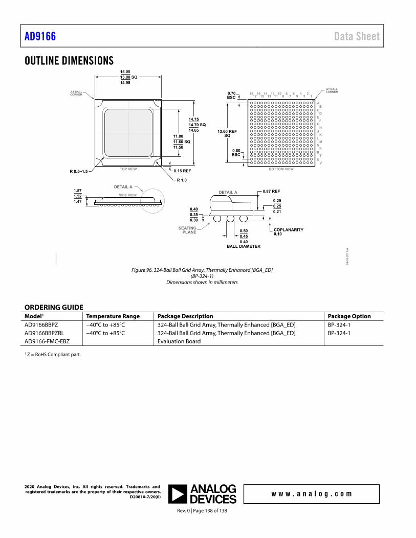
AD9166 Data Sheet
Rev. 0 | Page 138 of 138
OUTLINE DIMENSIONS
98
1110
1312
76
54 2
3 1
AB
CD
EF
GH
JK
LM
NP
RT
UV
1514
171618
PKG
-005
402
04-1
0-20
17-A
0.80BSC
BOTTOM VIEWTOP VIEW
SIDE VIEW
DETAIL A
15.0515.00 SQ14.95
14.7514.70 SQ14.65
11.8011.60 SQ11.50
1.571.521.47
13.60 REFSQ
0.70BSC
0.15 REF
A1 BALLCORNERA1 BALL
CORNER
0.290.250.210.40
0.350.30
0.87 REF
0.500.450.40
COPLANARITY0.10
BALL DIAMETER
DETAIL A
SEATINGPLANE
R 0.5~1.5
R 1.0
Figure 96. 324-Ball Ball Grid Array, Thermally Enhanced [BGA_ED]
(BP-324-1) Dimensions shown in millimeters
ORDERING GUIDE Model1 Temperature Range Package Description Package Option AD9166BBPZ −40°C to +85°C 324-Ball Ball Grid Array, Thermally Enhanced [BGA_ED] BP-324-1 AD9166BBPZRL −40°C to +85°C 324-Ball Ball Grid Array, Thermally Enhanced [BGA_ED] BP-324-1 AD9166-FMC-EBZ Evaluation Board 1 Z = RoHS Compliant part.
2020 Analog Devices, Inc. All rights reserved. Trademarks and registered trademarks are the property of their respective owners. D20810-7/20(0)
Related Documents