1778 IEEE TRANSACTIONS ON INDUSTRY APPLICATIONS, VOL. 47, NO. 4, JULY/AUGUST 2011 DC Bus Voltage Clamp Method to Prevent Over-Voltage Failures in Adjustable Speed Drives Lixiang Wei, Member, IEEE, Zhijun Liu, and Gary L. Skibinski Abstract—The influences of PWM switching and long cable length on motor insulations have been discussed in numerous pa- pers. This paper investigates their effect on the voltage insulation components inside an adjustable speed drive (ASD). This paper shows that high potential voltage insulation issue may exist on various components inside the ASD and cause earlier failures under very long cable or multiple drive conditions. A system model to describe this phenomenon is described in the paper. A dc bus voltage clamp circuit is proposed to reduce these voltage stresses. The effectiveness of this circuit is verified by both simulation and experimental results. Index Terms—Adjustable speed drive (ASD), insulation, long cable, voltage clamp circuit. I. I NTRODUCTION A DVANCES in power electronics technology has enabled the adjustable speed drive (ASD) to reach higher switch- ing and improved controllability of voltage, current and torque. Higher switching frequency may also reduce acoustic noise. The fast dv/dt PWM switching of the inverter devices also induce high frequency ground leakage current, high shaft in- sulation voltage, and high levels of bearing current. Numerous papers have been published to analyze these issues [1]–[11]. Chen and Lipo [1] pointed out that a net common-mode cur- rent flowing through three-phase stator windings to the axial direction produces a time-varying flux surrounding the motor shaft. This flux induces a shaft end-to-end voltage driving a circulating bearing current in turn. Reference [2]–[5] analyzed the PWM switching and cable length effect on bearing current, EMI emission, and motor insulation. In [4]–[12], various meth- ods and topologies were proposed to reduce the effect of the PWM switching on motor insulation, EMI performance and bearing current effect; However, they cannot reduce the voltage stresses inside the ASD drive. However, analysis of over voltage failures of components inside the drive has not been fully addressed. One simple assumption made from these references is that the common mode capacitance inside the drive is much higher than the Manuscript received October 16, 2010; revised December 13, 2010 and February 10, 2011; accepted February 17, 2011. Date of publication May 27, 2011; date of current version July 20, 2011. Paper 2010-IDC-415.R2, presented at the 2010 IEEE Energy Conversion Congress and Exposition, Atlanta, GA, September 12–16, and approved for publication in the IEEE TRANSACTIONS ON I NDUSTRY APPLICATIONS by the Industrial Drives Committee of the IEEE Industry Applications Society. The authors are with the Rockwell Automation-Allen Bradley, Mequon, WI 53092 USA (e-mail: [email protected]; [email protected]; [email protected]). Color versions of one or more of the figures in this paper are available online at http://ieeexplore.ieee.org. Digital Object Identifier 10.1109/TIA.2011.2154352 Fig. 1. Schematics of a standard ASD with common mode and cable models: (a) Diagram of an ASD drive with SCR front end; (b) Components that are exposed to high voltage stresses. common mode impedance external to the inverter. This is true for majority of applications. However, when an ASD is applied with very long cable or multiple parallel cables, common mode capacitance of the cable and motor may be comparable or even higher than the common mode capacitance inside the drive. Under this condition, high voltage stresses may be generated inside the drive. Fig. 1(a) shows a typical diagram of an ASD to be studied with SCR based rectifier. Fig. 1(b) further shows the voltage insulation components inside the ASD. Nowadays, the physical sizes of the ASD drive and its high voltage components have been reduced dramatically to remain competitive. Typical ways of reducing drive size is to replace the bus bars with printed circuit board (PCB), to integrate high voltage component with low voltage circuitry, to shrink the component sizes, and to reduce or remove unnecessary com- ponents. All above optimizations may increase voltage stresses of these components and cause unexpected voltage failures. This paper investigates the effects of PWM switching and long cable lengths on voltage stresses of different compo- nents inside the ASD. First, it categorizes the high voltage components and how to analyze their voltage stresses. It is found out that the voltage stresses of the component can be simplified by analyzing the voltage differences between dc bus terminals and the ground potential (GND). Then, a sys- tem model to describe this phenomenon is characterized and 0093-9994/$26.00 © 2011 IEEE

Welcome message from author
This document is posted to help you gain knowledge. Please leave a comment to let me know what you think about it! Share it to your friends and learn new things together.
Transcript
1778 IEEE TRANSACTIONS ON INDUSTRY APPLICATIONS, VOL. 47, NO. 4, JULY/AUGUST 2011
DC Bus Voltage Clamp Method to PreventOver-Voltage Failures in Adjustable Speed Drives
Lixiang Wei, Member, IEEE, Zhijun Liu, and Gary L. Skibinski
Abstract—The influences of PWM switching and long cablelength on motor insulations have been discussed in numerous pa-pers. This paper investigates their effect on the voltage insulationcomponents inside an adjustable speed drive (ASD). This papershows that high potential voltage insulation issue may exist onvarious components inside the ASD and cause earlier failuresunder very long cable or multiple drive conditions. A system modelto describe this phenomenon is described in the paper. A dc busvoltage clamp circuit is proposed to reduce these voltage stresses.The effectiveness of this circuit is verified by both simulation andexperimental results.
Index Terms—Adjustable speed drive (ASD), insulation, longcable, voltage clamp circuit.
I. INTRODUCTION
ADVANCES in power electronics technology has enabledthe adjustable speed drive (ASD) to reach higher switch-
ing and improved controllability of voltage, current and torque.Higher switching frequency may also reduce acoustic noise.The fast dv/dt PWM switching of the inverter devices alsoinduce high frequency ground leakage current, high shaft in-sulation voltage, and high levels of bearing current. Numerouspapers have been published to analyze these issues [1]–[11].Chen and Lipo [1] pointed out that a net common-mode cur-rent flowing through three-phase stator windings to the axialdirection produces a time-varying flux surrounding the motorshaft. This flux induces a shaft end-to-end voltage driving acirculating bearing current in turn. Reference [2]–[5] analyzedthe PWM switching and cable length effect on bearing current,EMI emission, and motor insulation. In [4]–[12], various meth-ods and topologies were proposed to reduce the effect of thePWM switching on motor insulation, EMI performance andbearing current effect; However, they cannot reduce the voltagestresses inside the ASD drive.
However, analysis of over voltage failures of componentsinside the drive has not been fully addressed. One simpleassumption made from these references is that the commonmode capacitance inside the drive is much higher than the
Manuscript received October 16, 2010; revised December 13, 2010 andFebruary 10, 2011; accepted February 17, 2011. Date of publication May 27,2011; date of current version July 20, 2011. Paper 2010-IDC-415.R2, presentedat the 2010 IEEE Energy Conversion Congress and Exposition, Atlanta, GA,September 12–16, and approved for publication in the IEEE TRANSACTIONS
ON INDUSTRY APPLICATIONS by the Industrial Drives Committee of the IEEEIndustry Applications Society.
The authors are with the Rockwell Automation-Allen Bradley, Mequon,WI 53092 USA (e-mail: [email protected]; [email protected];[email protected]).
Color versions of one or more of the figures in this paper are available onlineat http://ieeexplore.ieee.org.
Digital Object Identifier 10.1109/TIA.2011.2154352
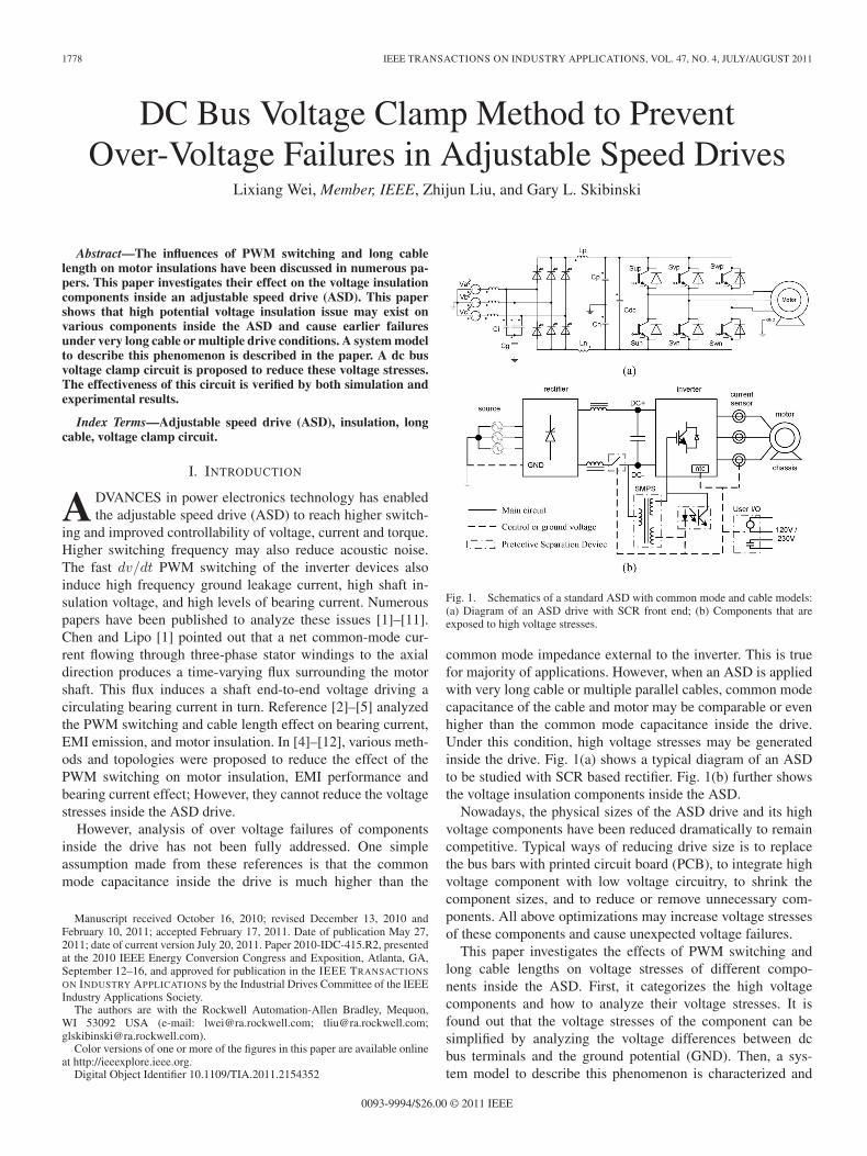
Fig. 1. Schematics of a standard ASD with common mode and cable models:(a) Diagram of an ASD drive with SCR front end; (b) Components that areexposed to high voltage stresses.
common mode impedance external to the inverter. This is truefor majority of applications. However, when an ASD is appliedwith very long cable or multiple parallel cables, common modecapacitance of the cable and motor may be comparable or evenhigher than the common mode capacitance inside the drive.Under this condition, high voltage stresses may be generatedinside the drive. Fig. 1(a) shows a typical diagram of an ASDto be studied with SCR based rectifier. Fig. 1(b) further showsthe voltage insulation components inside the ASD.
Nowadays, the physical sizes of the ASD drive and its highvoltage components have been reduced dramatically to remaincompetitive. Typical ways of reducing drive size is to replacethe bus bars with printed circuit board (PCB), to integrate highvoltage component with low voltage circuitry, to shrink thecomponent sizes, and to reduce or remove unnecessary com-ponents. All above optimizations may increase voltage stressesof these components and cause unexpected voltage failures.
This paper investigates the effects of PWM switching andlong cable lengths on voltage stresses of different compo-nents inside the ASD. First, it categorizes the high voltagecomponents and how to analyze their voltage stresses. It isfound out that the voltage stresses of the component can besimplified by analyzing the voltage differences between dcbus terminals and the ground potential (GND). Then, a sys-tem model to describe this phenomenon is characterized and
0093-9994/$26.00 © 2011 IEEE
WEI et al.: DC BUS VOLTAGE CLAMP METHOD TO PREVENT OVER-VOLTAGE FAILURES 1779
developed. It is found out that several potential high voltagestresses operating conditions (much higher than the dc busvoltage) may exist for some severe conditions.
After that, a simple dc bus voltage clamp circuit is intro-duced to help reduce the voltage stresses. This circuit has theminimum number of components—two diodes; one capacitor;and one resistor. It clamps the voltage stresses of the ASDdrive components to slightly higher than dc bus voltages. Oneadvantage of this circuit is that it only operates when the GNDis higher than dc+ or is lower than dc−. The wattage losses ofthe overall system and the voltage ratings of the dischargingcapacitors can be very low. Theory analysis, simulation andexperimental result are provided in the paper to verify theeffectiveness of the circuit.
II. VOLTAGE STRESSES IN ADJUSTABLE SPEED DRIVE
A. High Voltage Components and Their Voltage Stresses inASD Drive
One characteristic of ASDs is to use low voltage controlsignals to control high voltage switching devices. Based on theirfunctionality, there are two types of high voltage components.
The first type of components are the main circuit componentsthat transfer power from line to load side, including inverterIGBT, rectifier diode/SCR, dc link choke, dc bus capacitor,snubber capacitor, and etc. They are all located in the differen-tial mode (DM) circuit and their voltage stresses are generallyno higher than the dc bus voltage. Selection of voltage ratingsfor these components is straightforward.
The second type of components provide protective separationbetween the control circuit and the main circuit, includingopto-coupler, PCB, sensors, voltage/current transducer, switchmode power supply (SMPS) transformer, and etc. The highvoltage (HV) sides of these components are either no higherthan the positive bus or no lower than the negative bus. Thelow voltage (LV) sides are the control voltage that is veryclose to GND voltage. Therefore, the insulation voltage of theprotective separation component can be approximated as thevoltage between GND and the dc bus terminals. Selection ofthe voltage ratings for these components may be influenced bythe operating condition heavily and will be analyzed.
B. Differential Mode Voltage Between DC Bus Terminals tothe GND
The voltage stresses between the ground and the dc busterminals can be calculated by adding the common mode anddifferential mode components.
For the differential mode circuit, this voltage stresses canbe approximated as half the dc bus voltage for a Y groundedsystem. Where
Vpgpk_DM =Vdc
2; Vngpk_DM = −Vdc
2(1)
where Vpgpk_DM is the maximum voltage between positive dcbus and the GND in differential mode circuit, Vngpk_DM is theminimum voltage between negative bus voltage and the GNDin differential mode circuit.
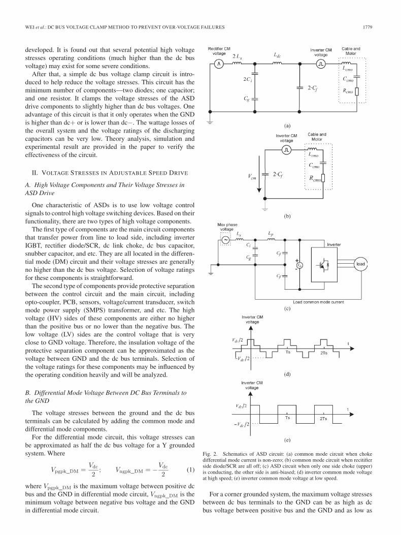
Fig. 2. Schematics of ASD circuit: (a) common mode circuit when chokedifferential mode current is non-zero; (b) common mode circuit when recitifierside diode/SCR are all off; (c) ASD circuit when only one side choke (upper)is conducting, the other side is anti-biased; (d) inverter common mode voltageat high speed; (e) inverter common mode voltage at low speed.
For a corner grounded system, the maximum voltage stressesbetween dc bus terminals to the GND can be as high as dcbus voltage between positive bus and the GND and as low as

1780 IEEE TRANSACTIONS ON INDUSTRY APPLICATIONS, VOL. 47, NO. 4, JULY/AUGUST 2011
Fig. 3. Proposed clamp ciricuit is a solid Y ground system.
negative dc bus voltage between negative bus to the GND asshown in
Vpgpk_DM = Vdc; Vngpk_DM = −Vdc. (2)
C. Common Mode Voltage Between DC Bus Terminalsand the GND
For the common mode voltage, it is determined by the cablelength, common mode capacitance of the ASD drive, and PWMswitching frequency. This voltage can be much higher than therated dc bus voltage for some cable and operating conditions asexplained in the following sections.
The main objective of this paper is to investigate the voltagestresses of insulation components inside a drive; the effectof the PWM switching to the motor winding and bearinginsulations will not be discussed. As a result, the common modemodel of the cable and motor is simplified as a single L–C–Rcircuit [6].
According to the conduction state of the input diode rectifier,there are three different simplified models of the common modecircuit for the ASD drive.
Figs. 2(a) and 3 show the equivalent circuit of common modecircuit when the rectifier has at least one switches of the upper(T1/T3/T5) diode/SCR and at least one switches of the lowerdiode/SCR (T2/T4/T6) conducting in the same time. Underthis condition, the common mode circuit and differential modecircuit are decoupled and it has been used as an equivalentcircuit of the system for most of the reference papers. Thecommon mode stresses generated by the PWM switching willbe distributed to rectifier side, dc bus, and the inverter sidecomponents. A much less voltage stresses is generated insidethe drive under this condition.
Fig. 2(a) is typical equivalent circuit discussed by mostresearchers. However, this is only true when the inverter isoperated under high loaded condition where the rectifier circuitoperates under continuous mode. There are two other operatingconditions exist when the rectifier operated under discontinuousmode. Both states may generate higher voltage stresses to thedrive components.
Fig. 2(b) shows an equivalent circuit of the drive when thereare no Diode/SCRs conducting. This operating state can befound widely when the rectifier has SCR switches. It existswhen the system operates at light load or regenerating conditionwhere both Diode/SCRs in the rectifier remains off state whilethe inverter is switching. Under this condition, the switchingenergy in the common mode circuit only distributed to the dc
bus terminals and the inverter side components. The voltagestresses of the drive components are generally higher thanFig. 2(a).
Fig. 2(c) shows the third equivalent circuits. Under this con-dition, only one side of the rectifier Diode/SCR is conducting.The common mode and differential mode circuit are combinedtogether and cannot be separated. For the case of Fig. 2(c),where only upper side diode/SCR are conducting, the upperside voltage potential between GND and dc+ are clamped bythe input circuit.
At low speed or no load condition, the system may transit be-tween these three conditions. As a result, the AC side commonmode capacitor maybe in and out of different equivalent circuitsand cause excessive voltages stresses between dc bus terminalsto GND.
The inverter common mode voltage is generated by the PWMswitching of the inverter. Fig. 2(d) shows a typical commonmode voltage generated by the PWM inverter at high speed.From this figure, the common mode voltage increase Vdc/3 ateach step. When the inverter operates at low speed, the highestcommon mode voltage steps generated as shown in Fig. 2(e). Inthis condition, the duty ratios of all three inverter legs are closeto 50%. The common mode voltage may change from Vdc/2 to−Vdc/2 directly as shown in Fig. 2(e).
It should be noted that some articles have proposed commonmode reduction PWM method (CMRPWM) for inverters [13].With this method, the zero vectors 000 and 111 are eliminatedto reduce the common mode stresses. Under this condition,the common mode voltage only increases Vdc/3 at each step.The voltage insulation between dc bus terminals to the GNDwill be reduced dramatically. However, this method does notcreate the best electrical performance to the system at lowspeed. It generates higher current stresses to dc bus capacitor,increase the harmonics and temperature of the motor windingand increase the audible noises at low speed. In this paper,only the standard PWM control method will be discussed torepresent the best electrical performance and the worst case forinsulation components inside the drive.
D. Voltage Stresses Analysis and the Capacitance RatioBetween ASD and the Load at Discontinuous Mode
For a RLC resonant circuit as shown in Fig. 2(b), a stepchange with an amplitude of Vdc in the common mode voltagecan induce as higher as two times of Vdc voltage spike in thecapacitor Cmo and 2 ∗ Cf if the effect of the resistance can beneglected. Thus, the worst case common mode voltage stress in

WEI et al.: DC BUS VOLTAGE CLAMP METHOD TO PREVENT OVER-VOLTAGE FAILURES 1781
Fig. 4. Worst-case peak common mode voltage between GND and the busterminals (Vdc is set as 640 V).
capacitor Cf generated by a single common mode voltage stepof Vdc (zero speed) can be calculated as
Vcmpk =2Vdc · Ccmo
Ccmo + 2 · Cf=
(2 − 4Cf
Ccmo + 2Cf
)Vdc (3)
where Cf is the common mode capacitor in dc link, the Ccmo isthe equivalent common mode capacitor of the cable and motor.
For majority of the applications, common mode filter capac-itor Cf is much higher than Ccmo. The peak common modevoltage stresses of Cf are low and the voltage potential of GNDis between dc+ and dc−. The voltage stresses of the protectiveinsulation components are low.
For some special conditions where multiple cables or verylong cables are associated, the total capacitance Ccmo may behigher than common mode capacitance Cf . The peak voltageinduced in the common mode capacitor will be increased to ashigh as twice the dc bus voltage. As a result, the voltage stressesof the protective separation component may be two times higherthan the dc bus voltage as shown in Fig. 4.
E. Overall Stresses Adding DM and CM Voltages
The worst case voltage stresses of between the dc bus to theGND adding differential mode voltage for Y grounded systemcan be expressed as
Vpg = Vpgpk_DM + Vcmpk =(
2.5 − 4Cf
Ccmo + 2Cf
)Vdc
Vng = Vngpk_DM − Vcmpk = −(
2.5 − 4Cf
Ccmo + 2Cf
)Vdc
(4)
where, Vpg/Vng is the voltage stresses between dc+ /dc− andGND, respectively
For corner grounded system, the worst case voltage stressesbetween the dc bus terminals to the GND adding differential
mode voltage can be expressed as
Vpg =Vpgpk_DM + Vcmpk =(
3 − 4Cf
Ccmo + 2Cf
)Vdc
Vng =Vngpk_DM − Vcmpk = −(
3 − 4Cf
Ccmo + 2Cf
)Vdc. (5)
Theoretically, the maximum voltage stresses existed betweendc bus terminals when the common mode capacitance Cf is 0and the inverter operated at low speed. It can reach as high as2.5 time of the dc bus voltage for Y grounded system and 3 timeof the dc bus voltage at corner grounded system. However, thisvalue is an ideal calculation by neglecting the damping of theoutput common mode circuit and the common mode capaci-tance of the power converter. Due to the conductor resistanceand insulation resistance between cable and the ground, thepeak voltage stress may never be able to reach this level.
III. PROPOSED VOLTAGE CLAMP METHOD
Fig. 4 show the proposed voltage clamp circuit for an ASDdrive. It consists of three types of components.
• Two diodes clamped between the positive and negative busvoltage.
• A clamping capacitor between the neutral of the twodiodes and the GND. The snubber capacitance is generallyselected to be higher than the common mode capacitanceof the cables and motors. The leakage inductance betweenthe capacitor to the dc bus terminal should be designed aslow as possible.
• A discharging resistor in parallel with the clampingcapacitor.
There are three operation modes of the clamp circuit.• Standby Mode: During normal condition, the voltage of
the GND is always lower than the dc+ and higher thandc−, both diodes are anti-biased. The voltage across theRC snubber circuit is zero as shown in Fig. 5(a).
• The voltage difference between GND and bus terminal isless than Vdc = Vdc+ − Vdc−.
• Clamping Mode: If the GND is either higher than dc+or lower than the dc−, one of the diode starts to conduct.The common mode energy will be transferred to the RCsnubber circuit, since the capacitance of this snubbercircuit is selected to be much higher than the overall cableand motor common mode capacitance. The potential of theGND will be clamped to one of the two dc bus voltages(dc+ or dc−). Fig. 5(b) shows a circuit diagram at thismode when Vgnd is higher than Vdc+. The voltage differ-ence between GND and bus terminal is slightly higher thanVdc = Vdc+ − Vdc−.
• Discharging Mode: After the PWM switching transientis over, the GND potential is low than dc+ and higherthan the dc−. Both diodes return to off condition. Theenergy of the snubber capacitor is now discharged bythe snubber resistor. After all energies are discharged, thesystem goes back to standby mode. The voltage differencebetween GND and bus terminal is still less than Vdc =Vdc+ − Vdc−.
1782 IEEE TRANSACTIONS ON INDUSTRY APPLICATIONS, VOL. 47, NO. 4, JULY/AUGUST 2011
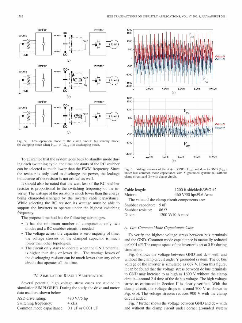
Fig. 5. Three operation mode of the clamp circuit: (a) standby mode;(b) clamping mode when Vgnd > Vdc+; (c) discharging mode.
To guarantee that the system goes back to standby mode dur-ing each switching cycle, the time constants of the RC snubbercan be selected as much lower than the PWM frequency. Sincethe resistor is only used to discharge the power, the leakageinductance of the resistor is not critical as well.
It should also be noted that the watt loss of the RC snubberresistor is proportional to the switching frequency of the in-verter. The wattage of the resistor is much lower than the energybeing charged/discharged by the inverter cable capacitance.While selecting the RC resistor, its wattage must be able tosupport the inverters to operate under the highest switchingfrequency.
The proposed method has the following advantages.
• It has the minimum number of components, only twodiodes and a RC snubber circuit is needed.
• The voltage across the capacitor is zero majority of time,the voltage stresses on the clamped capacitor is muchlower than other topologies.
• The circuit only starts to operate when the GND potentialis higher than dc+ or lower dc−. The wattage losses ofthe discharging resistor can be much lower than any othercircuit that operates all the time.
IV. SIMULATION RESULT VERIFICATION
Several potential high voltage stress cases are studied insimulation SIMPLORER. During the study, the drive and motordata used are shown below.ASD drive rating: 480 V/75 hpSwitching frequency: 4 kHzCommon mode capacitance: 0.1 uF or 0.001 uF
Fig. 6. Voltage stresses of the dc+ to GND (Vpg) and dc− to GND (Vng)under low common mode capacitance with Y grounded system: (a) withoutclamp circuit and (b) with clamp circuit.
Cable length: 1200 ft shielded/AWG #2Motor: 460 V/50 hp/59.6 Arms
The value of the clamp circuit components are:Snubber capacitor: 5 uFSnubber resistor: 86 ΩDiode: 1200 V/10 A rated
A. Low Common Mode Capacitance Case
To verify the highest voltage stress between bus terminalsand the GND. Common mode capacitance is manually reducedto 0.001 uF. The output speed of the inverter is set at 0 Hz duringsimulation.
Fig. 6 shows the voltage between GND and dc+ with andwithout the clamp circuit under Y grounded system. The dc busvoltage of the inverter is simulated as 667 V. From this figure,it can be found that the voltage stress between dc bus terminalsto GND may increase to as high as 1600 V without the clampcircuit—around 2.4 time of the dc bus voltage. The high voltagestress as estimated in Section II is clearly verified. With theclamp circuit, the voltage drops to around 700 V as shown inFig. 6(b). The voltage stresses reduces 900 V with the clampcircuit added.
Fig. 7 further shows the voltage between GND and dc+ withand without the clamp circuit under corner grounded system
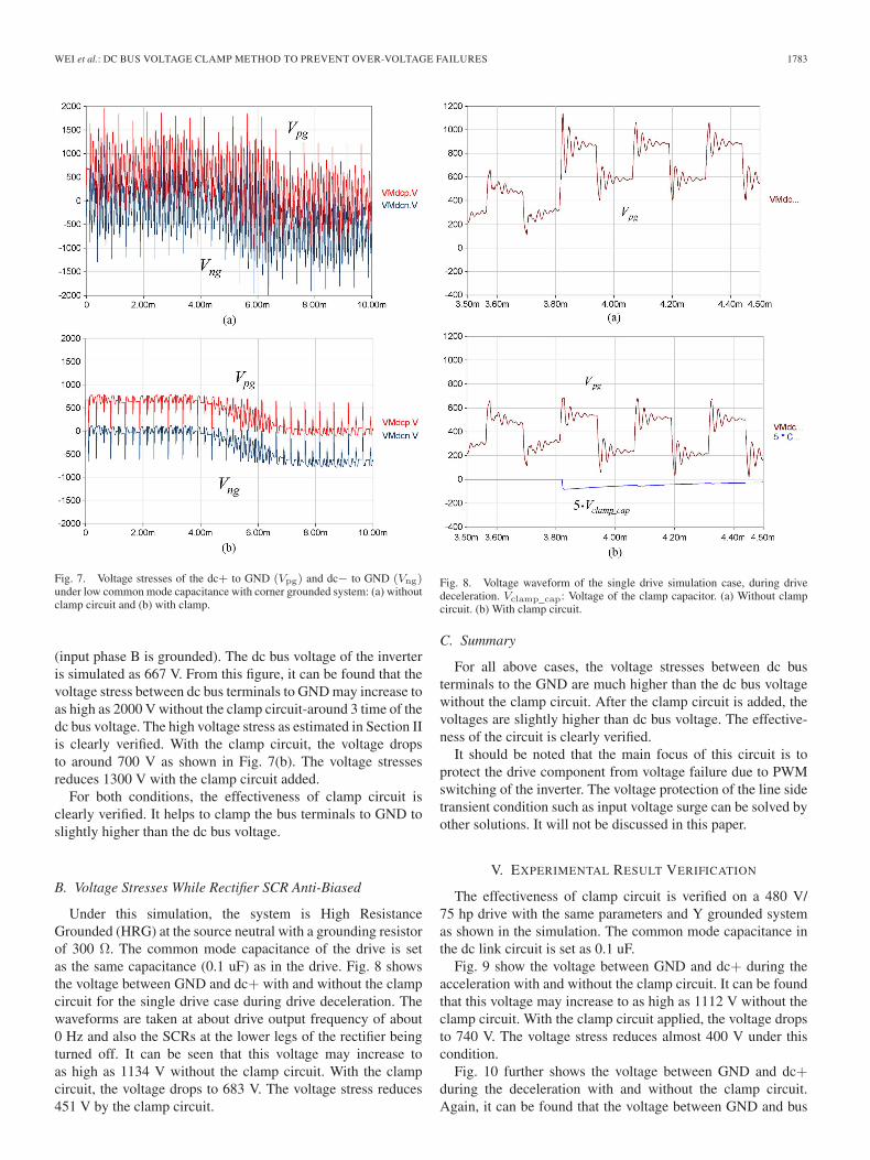
WEI et al.: DC BUS VOLTAGE CLAMP METHOD TO PREVENT OVER-VOLTAGE FAILURES 1783
Fig. 7. Voltage stresses of the dc+ to GND (Vpg) and dc− to GND (Vng)under low common mode capacitance with corner grounded system: (a) withoutclamp circuit and (b) with clamp.
(input phase B is grounded). The dc bus voltage of the inverteris simulated as 667 V. From this figure, it can be found that thevoltage stress between dc bus terminals to GND may increase toas high as 2000 V without the clamp circuit-around 3 time of thedc bus voltage. The high voltage stress as estimated in Section IIis clearly verified. With the clamp circuit, the voltage dropsto around 700 V as shown in Fig. 7(b). The voltage stressesreduces 1300 V with the clamp circuit added.
For both conditions, the effectiveness of clamp circuit isclearly verified. It helps to clamp the bus terminals to GND toslightly higher than the dc bus voltage.
B. Voltage Stresses While Rectifier SCR Anti-Biased
Under this simulation, the system is High ResistanceGrounded (HRG) at the source neutral with a grounding resistorof 300 Ω. The common mode capacitance of the drive is setas the same capacitance (0.1 uF) as in the drive. Fig. 8 showsthe voltage between GND and dc+ with and without the clampcircuit for the single drive case during drive deceleration. Thewaveforms are taken at about drive output frequency of about0 Hz and also the SCRs at the lower legs of the rectifier beingturned off. It can be seen that this voltage may increase toas high as 1134 V without the clamp circuit. With the clampcircuit, the voltage drops to 683 V. The voltage stress reduces451 V by the clamp circuit.
Fig. 8. Voltage waveform of the single drive simulation case, during drivedeceleration. Vclamp_cap: Voltage of the clamp capacitor. (a) Without clampcircuit. (b) With clamp circuit.
C. Summary
For all above cases, the voltage stresses between dc busterminals to the GND are much higher than the dc bus voltagewithout the clamp circuit. After the clamp circuit is added, thevoltages are slightly higher than dc bus voltage. The effective-ness of the circuit is clearly verified.
It should be noted that the main focus of this circuit is toprotect the drive component from voltage failure due to PWMswitching of the inverter. The voltage protection of the line sidetransient condition such as input voltage surge can be solved byother solutions. It will not be discussed in this paper.
V. EXPERIMENTAL RESULT VERIFICATION
The effectiveness of clamp circuit is verified on a 480 V/75 hp drive with the same parameters and Y grounded systemas shown in the simulation. The common mode capacitance inthe dc link circuit is set as 0.1 uF.
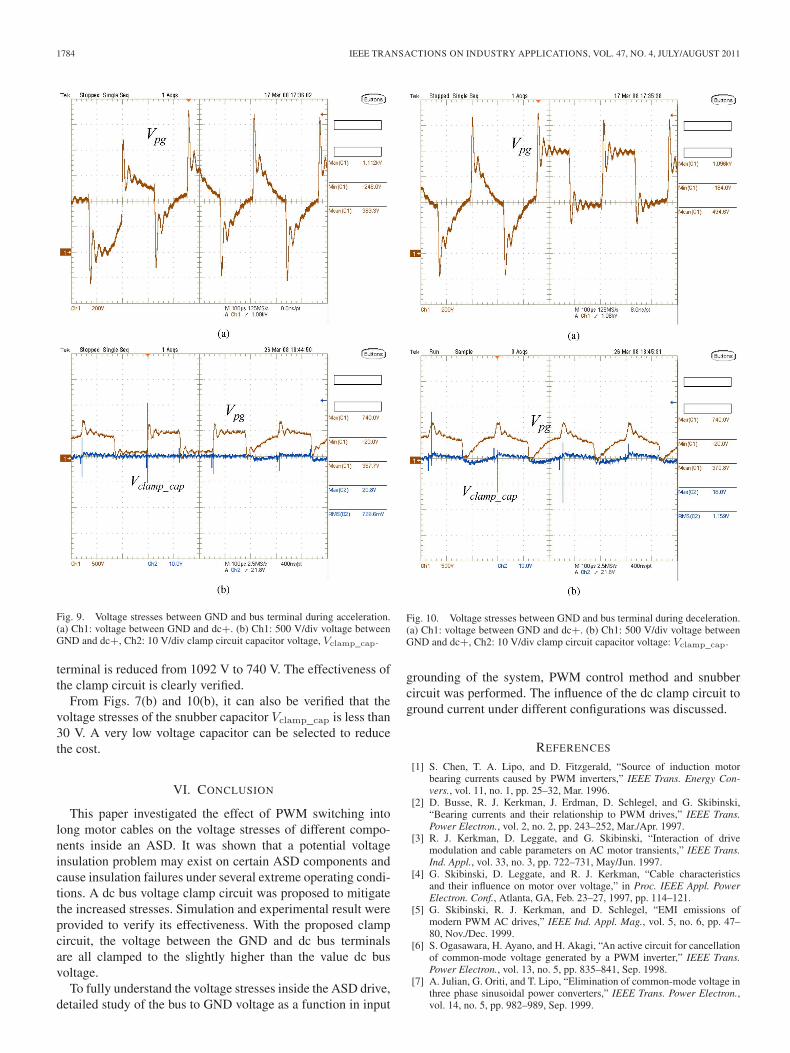
Fig. 9 show the voltage between GND and dc+ during theacceleration with and without the clamp circuit. It can be foundthat this voltage may increase to as high as 1112 V without theclamp circuit. With the clamp circuit applied, the voltage dropsto 740 V. The voltage stress reduces almost 400 V under thiscondition.
Fig. 10 further shows the voltage between GND and dc+during the deceleration with and without the clamp circuit.Again, it can be found that the voltage between GND and bus
1784 IEEE TRANSACTIONS ON INDUSTRY APPLICATIONS, VOL. 47, NO. 4, JULY/AUGUST 2011
Fig. 9. Voltage stresses between GND and bus terminal during acceleration.(a) Ch1: voltage between GND and dc+. (b) Ch1: 500 V/div voltage betweenGND and dc+, Ch2: 10 V/div clamp circuit capacitor voltage, Vclamp_cap.
terminal is reduced from 1092 V to 740 V. The effectiveness ofthe clamp circuit is clearly verified.
From Figs. 7(b) and 10(b), it can also be verified that thevoltage stresses of the snubber capacitor Vclamp_cap is less than30 V. A very low voltage capacitor can be selected to reducethe cost.
VI. CONCLUSION
This paper investigated the effect of PWM switching intolong motor cables on the voltage stresses of different compo-nents inside an ASD. It was shown that a potential voltageinsulation problem may exist on certain ASD components andcause insulation failures under several extreme operating condi-tions. A dc bus voltage clamp circuit was proposed to mitigatethe increased stresses. Simulation and experimental result wereprovided to verify its effectiveness. With the proposed clampcircuit, the voltage between the GND and dc bus terminalsare all clamped to the slightly higher than the value dc busvoltage.
To fully understand the voltage stresses inside the ASD drive,detailed study of the bus to GND voltage as a function in input
Fig. 10. Voltage stresses between GND and bus terminal during deceleration.(a) Ch1: voltage between GND and dc+. (b) Ch1: 500 V/div voltage betweenGND and dc+, Ch2: 10 V/div clamp circuit capacitor voltage: Vclamp_cap.
grounding of the system, PWM control method and snubbercircuit was performed. The influence of the dc clamp circuit toground current under different configurations was discussed.
REFERENCES
[1] S. Chen, T. A. Lipo, and D. Fitzgerald, “Source of induction motorbearing currents caused by PWM inverters,” IEEE Trans. Energy Con-vers., vol. 11, no. 1, pp. 25–32, Mar. 1996.
[2] D. Busse, R. J. Kerkman, J. Erdman, D. Schlegel, and G. Skibinski,“Bearing currents and their relationship to PWM drives,” IEEE Trans.Power Electron., vol. 2, no. 2, pp. 243–252, Mar./Apr. 1997.
[3] R. J. Kerkman, D. Leggate, and G. Skibinski, “Interaction of drivemodulation and cable parameters on AC motor transients,” IEEE Trans.Ind. Appl., vol. 33, no. 3, pp. 722–731, May/Jun. 1997.
[4] G. Skibinski, D. Leggate, and R. J. Kerkman, “Cable characteristicsand their influence on motor over voltage,” in Proc. IEEE Appl. PowerElectron. Conf., Atlanta, GA, Feb. 23–27, 1997, pp. 114–121.
[5] G. Skibinski, R. J. Kerkman, and D. Schlegel, “EMI emissions ofmodern PWM AC drives,” IEEE Ind. Appl. Mag., vol. 5, no. 6, pp. 47–80, Nov./Dec. 1999.
[6] S. Ogasawara, H. Ayano, and H. Akagi, “An active circuit for cancellationof common-mode voltage generated by a PWM inverter,” IEEE Trans.Power Electron., vol. 13, no. 5, pp. 835–841, Sep. 1998.
[7] A. Julian, G. Oriti, and T. Lipo, “Elimination of common-mode voltage inthree phase sinusoidal power converters,” IEEE Trans. Power Electron.,vol. 14, no. 5, pp. 982–989, Sep. 1999.

WEI et al.: DC BUS VOLTAGE CLAMP METHOD TO PREVENT OVER-VOLTAGE FAILURES 1785
[8] M. M. Swamy, K. Yamada, and T. Kume, “Common mode currentattenuation techniques for use with PWM drives,” IEEE Trans. PowerElectron., vol. 16, no. 2, pp. 248–255, Mar. 2001.
[9] Y. C. Son and S. K. Sul, “A new active common-mode filter for PWMinverter,” IEEE Trans. Power Electron., vol. 18, no. 6, pp. 1309–1314,Nov. 2003.
[10] D. Hyypio, “Mitigation of bearing electro-erosion of inverter-fed motorsthrough passive common-mode voltage suppression,” IEEE Trans. Ind.Appl., vol. 41, no. 2, pp. 576–583, Mar./Apr. 2005.
[11] H. Akagi and T. Doumoto, “An approach to eliminating high-frequencyshaft voltage and leakage current from an inverter-driven motor,” IEEETrans. Ind. Appl., vol. 40, no. 4, pp. 1162–1169, Jul./Aug. 2004.
[12] D. Gritter and J. Reichard, “DV/DT limiting of inverter output voltage,”U.S. Patent 5 633 790, May 27, 1997.
[13] A. Hava and E. Un, “Performance analysis of reduced common modevoltage PWM methods and comparison with standard PWM methodsfor three phase voltage source inverters,” IEEE Trans. Power Electron.,vol. 24, no. 1, pp. 241–252, Jan. 2009.
Lixiang Wei (S’98–A’00–M’03) was born in Chinain 1973. He received the Ph.D. degree in electri-cal engineering from the University of Wisconsin-Madison, Madison, in 2003.
He is currently employed as a Principal Engi-neer with Standard Drive Division of RockwellAutomation-Allen Bradley, Mequon, WI. He hasinvolved in research and development of power elec-tronics and motor drive area for over 10 years. He isthe author of more than 30 international journal andconference papers and received three IAS committee
paper prizes. He is also the author of 12 U.S. patents and has more than30 other U.S. patents pending. His main research areas are power converterdesign, thermal analysis of multiple-chip power modules, filter and magneticdesign, low power and high power converter design, and various motor controlsystems.
Dr. Wei is currently the Chair of Industrial Power Converter Committee ofIEEE Industry Application Society.
Zhijun Liu received the B.S. and M.S. degreesin electrical engineering from Harbin Institute ofTechnology, Harbin, China, in 1982 and 1985,respectively, and the D.Eng. degree from ClevelandState University, Cleveland, OH, in 1993.
From 1993 to 1995, he was an Electrical En-gineer at Electric Systems, Inc., Chattanooga, TN.Since 1995, he has been employed with RockwellAutomation-Allen Bradley, Mequon, WI, where heis currently a Project Engineer in the Systems andSolutions Business. His research interests are in the
areas of power electronics and ac drives, control systems and algorithms,system modeling and analysis, and application of drive systems in industrialprocess lines.
Gary L. Skibinski received B.S. and M.S. degreesin electrical engineering from the University ofWisconsin, Milwaukee, and the Ph.D. degree fromthe University of Wisconsin-Madison, Madison, in1976, 1980, and 1992, respectively.
From 1976 to 1980, he was an Electrical Engineerworking on naval nuclear power converters at Eaton.From 1981 to 1985, he worked as Senior Project En-gineer at Allen-Bradley on servo controllers. Duringthe Ph.D. program, he was a Consultant for UPSand switch-mode power supply products at R.T.E.
Corporation He is currently Engineering Fellow at Rockwell Automation-AllenBradley, Mequon, WI. His current interests include power semiconductors,power electronic applications, and high-frequency high-power converter cir-cuits for ac drives. He is the holder of 29 U.S. patents, published articlesin two IEEE press books, published over 80 articles in professional journals/conferences with nineteen being prize awards and is a registered PE in the stateof Wisconsin.
Dr. Skibinski is the Chairman of IEEE Std. 518 Guide for the Installation ofElectrical Equipment to Minimize Electrical Noise.
Related Documents


