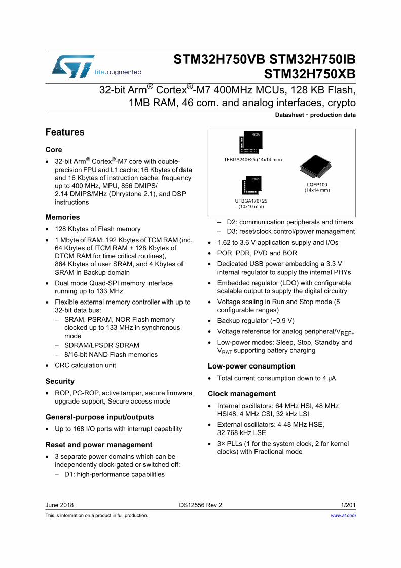
This is information on a product in full production. June 2018 DS12556 Rev 2 1/201 STM32H750VB STM32H750IB STM32H750XB 32-bit Arm ® Cortex ® -M7 400MHz MCUs, 128 KB Flash, 1MB RAM, 46 com. and analog interfaces, crypto Datasheet - production data Features Core • 32-bit Arm ® Cortex ® -M7 core with double- precision FPU and L1 cache: 16 Kbytes of data and 16 Kbytes of instruction cache; frequency up to 400 MHz, MPU, 856 DMIPS/ 2.14 DMIPS/MHz (Dhrystone 2.1), and DSP instructions Memories • 128 Kbytes of Flash memory • 1 Mbyte of RAM: 192 Kbytes of TCM RAM (inc. 64 Kbytes of ITCM RAM + 128 Kbytes of DTCM RAM for time critical routines), 864 Kbytes of user SRAM, and 4 Kbytes of SRAM in Backup domain • Dual mode Quad-SPI memory interface running up to 133 MHz • Flexible external memory controller with up to 32-bit data bus: – SRAM, PSRAM, NOR Flash memory clocked up to 133 MHz in synchronous mode – SDRAM/LPSDR SDRAM – 8/16-bit NAND Flash memories • CRC calculation unit Security • ROP, PC-ROP, active tamper, secure firmware upgrade support, Secure access mode General-purpose input/outputs • Up to 168 I/O ports with interrupt capability Reset and power management • 3 separate power domains which can be independently clock-gated or switched off: – D1: high-performance capabilities – D2: communication peripherals and timers – D3: reset/clock control/power management • 1.62 to 3.6 V application supply and I/Os • POR, PDR, PVD and BOR • Dedicated USB power embedding a 3.3 V internal regulator to supply the internal PHYs • Embedded regulator (LDO) with configurable scalable output to supply the digital circuitry • Voltage scaling in Run and Stop mode (5 configurable ranges) • Backup regulator (~0.9 V) • Voltage reference for analog peripheral/V REF+ • Low-power modes: Sleep, Stop, Standby and V BAT supporting battery charging Low-power consumption • Total current consumption down to 4 μA Clock management • Internal oscillators: 64 MHz HSI, 48 MHz HSI48, 4 MHz CSI, 32 kHz LSI • External oscillators: 4-48 MHz HSE, 32.768 kHz LSE • 3× PLLs (1 for the system clock, 2 for kernel clocks) with Fractional mode FBGA LQFP100 (14x14 mm) UFBGA176+25 (10x10 mm) FBGA TFBGA240+25 (14x14 mm) www.st.com

Welcome message from author
This document is posted to help you gain knowledge. Please leave a comment to let me know what you think about it! Share it to your friends and learn new things together.
Transcript
This is information on a product in full production.
June 2018 DS12556 Rev 2 1/201
STM32H750VB STM32H750IB STM32H750XB
32-bit Arm® Cortex®-M7 400MHz MCUs, 128 KB Flash, 1MB RAM, 46 com. and analog interfaces, crypto
Datasheet - production data
Features
Core
• 32-bit Arm® Cortex®-M7 core with double-precision FPU and L1 cache: 16 Kbytes of data and 16 Kbytes of instruction cache; frequency up to 400 MHz, MPU, 856 DMIPS/ 2.14 DMIPS/MHz (Dhrystone 2.1), and DSP instructions
Memories
• 128 Kbytes of Flash memory
• 1 Mbyte of RAM: 192 Kbytes of TCM RAM (inc. 64 Kbytes of ITCM RAM + 128 Kbytes of DTCM RAM for time critical routines), 864 Kbytes of user SRAM, and 4 Kbytes of SRAM in Backup domain
• Dual mode Quad-SPI memory interface running up to 133 MHz
• Flexible external memory controller with up to 32-bit data bus:
– SRAM, PSRAM, NOR Flash memory clocked up to 133 MHz in synchronous mode
– SDRAM/LPSDR SDRAM
– 8/16-bit NAND Flash memories
• CRC calculation unit
Security
• ROP, PC-ROP, active tamper, secure firmware upgrade support, Secure access mode
General-purpose input/outputs
• Up to 168 I/O ports with interrupt capability
Reset and power management
• 3 separate power domains which can be independently clock-gated or switched off:
– D1: high-performance capabilities
– D2: communication peripherals and timers
– D3: reset/clock control/power management
• 1.62 to 3.6 V application supply and I/Os
• POR, PDR, PVD and BOR
• Dedicated USB power embedding a 3.3 V internal regulator to supply the internal PHYs
• Embedded regulator (LDO) with configurable scalable output to supply the digital circuitry
• Voltage scaling in Run and Stop mode (5 configurable ranges)
• Backup regulator (~0.9 V)
• Voltage reference for analog peripheral/VREF+
• Low-power modes: Sleep, Stop, Standby and VBAT supporting battery charging
Low-power consumption
• Total current consumption down to 4 µA
Clock management
• Internal oscillators: 64 MHz HSI, 48 MHz HSI48, 4 MHz CSI, 32 kHz LSI
• External oscillators: 4-48 MHz HSE, 32.768 kHz LSE
• 3× PLLs (1 for the system clock, 2 for kernel clocks) with Fractional mode
FBGA
LQFP100(14x14 mm)
UFBGA176+25 (10x10 mm)
FBGA
TFBGA240+25 (14x14 mm)
www.st.com
STM32H750VB STM32H750IB STM32H750XB
2/201 DS12556 Rev 2
Interconnect matrix
• 3 bus matrices (1 AXI and 2 AHB)
• Bridges (5× AHB2-APB, 2× AXI2-AHB)
4 DMA controllers to unload the CPU
• 1× high-speed master direct memory access controller (MDMA) with linked list support
• 2× dual-port DMAs with FIFO
• 1× basic DMA with request router capabilities
Up to 35 communication peripherals
• 4× I2Cs FM+ interfaces (SMBus/PMBus)
• 4× USARTs/4x UARTs (ISO7816 interface, LIN, IrDA, up to 12.5 Mbit/s) and 1x LPUART
• 6× SPIs, 3 with muxed duplex I2S audio class accuracy via internal audio PLL or external clock, 1x I2S in LP domain (up to 133 MHz)
• 4x SAIs (serial audio interface)
• SPDIFRX interface
• SWPMI single-wire protocol master I/F
• MDIO Slave interface
• 2× SD/SDIO/MMC interfaces (up to 125 MHz)
• 2× CAN controllers: 2 with CAN FD, 1 with time-triggered CAN (TT-CAN)
• 2× USB OTG interfaces (1FS, 1HS/FS) crystal-less solution with LPM and BCD
• Ethernet MAC interface with DMA controller
• HDMI-CEC
• 8- to 14-bit camera interface (up to 80 MHz)
11 analog peripherals
• 3× ADCs with 16-bit max. resolution (up to 36 channels, 4.5 MSPS at 12 bits)
• 1× temperature sensor
• 2× 12-bit D/A converters (1 MHz)
• 2× ultra-low-power comparators
• 2× operational amplifiers (8 MHz bandwidth)
• 1× digital filters for sigma delta modulator (DFSDM) with 8 channels/4 filters
Graphics
• LCD-TFT controller up to XGA resolution
• Chrom-ART graphical hardware Accelerator™ (DMA2D) to reduce CPU load
• Hardware JPEG Codec
Up to 22 timers and watchdogs
• 1× high-resolution timer (2.5 ns max resolution)
• 2× 32-bit timers with up to 4 IC/OC/PWM or pulse counter and quadrature (incremental) encoder input (up to 200 MHz)
• 2× 16-bit advanced motor control timers (up to 200 MHz)
• 10× 16-bit general-purpose timers (up to 200 MHz)
• 5× 16-bit low-power timers (up to 200 MHz)
• 2× watchdogs (independent and window)
• 1× SysTick timer
• RTC with sub-second accuracy & HW calendar
Cryptographic acceleration
• AES 128, 192, 256, TDES,
• HASH (MD5, SHA-1, SHA-2), HMAC
• True random number generators
Debug mode
• SWD & JTAG interfaces
• 4-Kbyte Embedded Trace Buffer
96-bit unique ID
All packages are ECOPACK®2 compliant

DS12556 Rev 2 3/201
STM32H750VB STM32H750IB STM32H750XB Contents
6
Contents
1 Introduction . . . . . . . . . . . . . . . . . . . . . . . . . . . . . . . . . . . . . . . . . . . . . . . 12
2 Description . . . . . . . . . . . . . . . . . . . . . . . . . . . . . . . . . . . . . . . . . . . . . . . . 13
3 Functional overview . . . . . . . . . . . . . . . . . . . . . . . . . . . . . . . . . . . . . . . . 18
3.1 Arm® Cortex®-M7 with FPU . . . . . . . . . . . . . . . . . . . . . . . . . . . . . . . . . . . 18
3.2 Memory protection unit (MPU) . . . . . . . . . . . . . . . . . . . . . . . . . . . . . . . . . 18
3.3 Memories . . . . . . . . . . . . . . . . . . . . . . . . . . . . . . . . . . . . . . . . . . . . . . . . . 19
3.3.1 Embedded Flash memory . . . . . . . . . . . . . . . . . . . . . . . . . . . . . . . . . . . 19
3.3.2 Secure access mode . . . . . . . . . . . . . . . . . . . . . . . . . . . . . . . . . . . . . . . 19
3.3.3 Embedded SRAM . . . . . . . . . . . . . . . . . . . . . . . . . . . . . . . . . . . . . . . . . 20
3.4 Boot modes . . . . . . . . . . . . . . . . . . . . . . . . . . . . . . . . . . . . . . . . . . . . . . . 20
3.5 Power supply management . . . . . . . . . . . . . . . . . . . . . . . . . . . . . . . . . . . 21
3.5.1 Power supply scheme . . . . . . . . . . . . . . . . . . . . . . . . . . . . . . . . . . . . . . 21
3.5.2 Power supply supervisor . . . . . . . . . . . . . . . . . . . . . . . . . . . . . . . . . . . . 22
3.5.3 Voltage regulator . . . . . . . . . . . . . . . . . . . . . . . . . . . . . . . . . . . . . . . . . . 23
3.6 Low-power strategy . . . . . . . . . . . . . . . . . . . . . . . . . . . . . . . . . . . . . . . . . 23
3.7 Reset and clock controller (RCC) . . . . . . . . . . . . . . . . . . . . . . . . . . . . . . . 24
3.7.1 Clock management . . . . . . . . . . . . . . . . . . . . . . . . . . . . . . . . . . . . . . . . 24
3.7.2 System reset sources . . . . . . . . . . . . . . . . . . . . . . . . . . . . . . . . . . . . . . 25
3.8 General-purpose input/outputs (GPIOs) . . . . . . . . . . . . . . . . . . . . . . . . . . 25
3.9 Bus-interconnect matrix . . . . . . . . . . . . . . . . . . . . . . . . . . . . . . . . . . . . . . 25
3.10 DMA controllers . . . . . . . . . . . . . . . . . . . . . . . . . . . . . . . . . . . . . . . . . . . . 27
3.11 Chrom-ART Accelerator™ (DMA2D) . . . . . . . . . . . . . . . . . . . . . . . . . . . . 27
3.12 Nested vectored interrupt controller (NVIC) . . . . . . . . . . . . . . . . . . . . . . . 28
3.13 Extended interrupt and event controller (EXTI) . . . . . . . . . . . . . . . . . . . . 28
3.14 Cyclic redundancy check calculation unit (CRC) . . . . . . . . . . . . . . . . . . . 28
3.15 Flexible memory controller (FMC) . . . . . . . . . . . . . . . . . . . . . . . . . . . . . . 29
3.16 Quad-SPI memory interface (QUADSPI) . . . . . . . . . . . . . . . . . . . . . . . . . 29
3.17 Analog-to-digital converters (ADCs) . . . . . . . . . . . . . . . . . . . . . . . . . . . . . 29
3.18 Temperature sensor . . . . . . . . . . . . . . . . . . . . . . . . . . . . . . . . . . . . . . . . . 30
3.19 VBAT operation . . . . . . . . . . . . . . . . . . . . . . . . . . . . . . . . . . . . . . . . . . . . . 30
Contents STM32H750VB STM32H750IB STM32H750XB
4/201 DS12556 Rev 2
3.20 Digital-to-analog converters (DAC) . . . . . . . . . . . . . . . . . . . . . . . . . . . . . 31
3.21 Ultra-low-power comparators (COMP) . . . . . . . . . . . . . . . . . . . . . . . . . . . 31
3.22 Operational amplifiers (OPAMP) . . . . . . . . . . . . . . . . . . . . . . . . . . . . . . . 31
3.23 Digital filter for sigma-delta modulators (DFSDM) . . . . . . . . . . . . . . . . . . 32
3.24 Digital camera interface (DCMI) . . . . . . . . . . . . . . . . . . . . . . . . . . . . . . . . 33
3.25 LCD-TFT controller . . . . . . . . . . . . . . . . . . . . . . . . . . . . . . . . . . . . . . . . . . 34
3.26 JPEG Codec (JPEG) . . . . . . . . . . . . . . . . . . . . . . . . . . . . . . . . . . . . . . . . 34
3.27 Random number generator (RNG) . . . . . . . . . . . . . . . . . . . . . . . . . . . . . . 34
3.28 Cryptographic acceleration (CRYPT and HASH) . . . . . . . . . . . . . . . . . . . 35
3.29 Timers and watchdogs . . . . . . . . . . . . . . . . . . . . . . . . . . . . . . . . . . . . . . . 35
3.29.1 High-resolution timer (HRTIM1) . . . . . . . . . . . . . . . . . . . . . . . . . . . . . . . 37
3.29.2 Advanced-control timers (TIM1, TIM8) . . . . . . . . . . . . . . . . . . . . . . . . . 38
3.29.3 General-purpose timers (TIMx) . . . . . . . . . . . . . . . . . . . . . . . . . . . . . . . 38
3.29.4 Basic timers TIM6 and TIM7 . . . . . . . . . . . . . . . . . . . . . . . . . . . . . . . . . 39
3.29.5 Low-power timers (LPTIM1, LPTIM2, LPTIM3, LPTIM4, LPTIM5) . . . . 39
3.29.6 Independent watchdog . . . . . . . . . . . . . . . . . . . . . . . . . . . . . . . . . . . . . 39
3.29.7 Window watchdog . . . . . . . . . . . . . . . . . . . . . . . . . . . . . . . . . . . . . . . . . 39
3.29.8 SysTick timer . . . . . . . . . . . . . . . . . . . . . . . . . . . . . . . . . . . . . . . . . . . . . 39
3.30 Real-time clock (RTC), backup SRAM and backup registers . . . . . . . . . . 40
3.31 Inter-integrated circuit interface (I2C) . . . . . . . . . . . . . . . . . . . . . . . . . . . . 41
3.32 Universal synchronous/asynchronous receiver transmitter (USART) . . . 41
3.33 Low-power universal asynchronous receiver transmitter (LPUART) . . . . 42
3.34 Serial peripheral interface (SPI)/inter- integrated sound interfaces (I2S) . 43
3.35 Serial audio interfaces (SAI) . . . . . . . . . . . . . . . . . . . . . . . . . . . . . . . . . . . 43
3.36 SPDIFRX Receiver Interface (SPDIFRX) . . . . . . . . . . . . . . . . . . . . . . . . . 44
3.37 Single wire protocol master interface (SWPMI) . . . . . . . . . . . . . . . . . . . . 44
3.38 Management Data Input/Output (MDIO) slaves . . . . . . . . . . . . . . . . . . . . 45
3.39 SD/SDIO/MMC card host interfaces (SDMMC) . . . . . . . . . . . . . . . . . . . . 45
3.40 Controller area network (FDCAN1, FDCAN2) . . . . . . . . . . . . . . . . . . . . . 45
3.41 Universal serial bus on-the-go high-speed (OTG_HS) . . . . . . . . . . . . . . . 46
3.42 Ethernet MAC interface with dedicated DMA controller (ETH) . . . . . . . . . 46
3.43 High-definition multimedia interface (HDMI) - consumer electronics control (CEC) . . . . . . . . . . . . . . . . . . . . . . . . . . . 47
3.44 Debug infrastructure . . . . . . . . . . . . . . . . . . . . . . . . . . . . . . . . . . . . . . . . . 47

DS12556 Rev 2 5/201
STM32H750VB STM32H750IB STM32H750XB Contents
6
4 Memory mapping . . . . . . . . . . . . . . . . . . . . . . . . . . . . . . . . . . . . . . . . . . . 48
5 Pin descriptions . . . . . . . . . . . . . . . . . . . . . . . . . . . . . . . . . . . . . . . . . . . 49
6 Electrical characteristics . . . . . . . . . . . . . . . . . . . . . . . . . . . . . . . . . . . . 86
6.1 Parameter conditions . . . . . . . . . . . . . . . . . . . . . . . . . . . . . . . . . . . . . . . . 86
6.1.1 Minimum and maximum values . . . . . . . . . . . . . . . . . . . . . . . . . . . . . . . 86
6.1.2 Typical values . . . . . . . . . . . . . . . . . . . . . . . . . . . . . . . . . . . . . . . . . . . . 86
6.1.3 Typical curves . . . . . . . . . . . . . . . . . . . . . . . . . . . . . . . . . . . . . . . . . . . . 86
6.1.4 Loading capacitor . . . . . . . . . . . . . . . . . . . . . . . . . . . . . . . . . . . . . . . . . 86
6.1.5 Pin input voltage . . . . . . . . . . . . . . . . . . . . . . . . . . . . . . . . . . . . . . . . . . 86
6.1.6 Power supply scheme . . . . . . . . . . . . . . . . . . . . . . . . . . . . . . . . . . . . . . 87
6.1.7 Current consumption measurement . . . . . . . . . . . . . . . . . . . . . . . . . . . 88
6.2 Absolute maximum ratings . . . . . . . . . . . . . . . . . . . . . . . . . . . . . . . . . . . . 88
6.3 Operating conditions . . . . . . . . . . . . . . . . . . . . . . . . . . . . . . . . . . . . . . . . 90
6.3.1 General operating conditions . . . . . . . . . . . . . . . . . . . . . . . . . . . . . . . . . 90
6.3.2 VCAP external capacitor . . . . . . . . . . . . . . . . . . . . . . . . . . . . . . . . . . . . 91
6.3.3 Operating conditions at power-up / power-down . . . . . . . . . . . . . . . . . . 91
6.3.4 Embedded reset and power control block characteristics . . . . . . . . . . . 92
6.3.5 Embedded reference voltage . . . . . . . . . . . . . . . . . . . . . . . . . . . . . . . . . 93
6.3.6 Supply current characteristics . . . . . . . . . . . . . . . . . . . . . . . . . . . . . . . . 94
6.3.7 Wakeup time from low-power modes . . . . . . . . . . . . . . . . . . . . . . . . . . 107
6.3.8 External clock source characteristics . . . . . . . . . . . . . . . . . . . . . . . . . . 108
6.3.9 Internal clock source characteristics . . . . . . . . . . . . . . . . . . . . . . . . . . 112
6.3.10 PLL characteristics . . . . . . . . . . . . . . . . . . . . . . . . . . . . . . . . . . . . . . . . 114
6.3.11 Memory characteristics . . . . . . . . . . . . . . . . . . . . . . . . . . . . . . . . . . . . 116
6.3.12 EMC characteristics . . . . . . . . . . . . . . . . . . . . . . . . . . . . . . . . . . . . . . . 118
6.3.13 Absolute maximum ratings (electrical sensitivity) . . . . . . . . . . . . . . . . 119
6.3.14 I/O current injection characteristics . . . . . . . . . . . . . . . . . . . . . . . . . . . 120
6.3.15 I/O port characteristics . . . . . . . . . . . . . . . . . . . . . . . . . . . . . . . . . . . . . 121
6.3.16 NRST pin characteristics . . . . . . . . . . . . . . . . . . . . . . . . . . . . . . . . . . . 127
6.3.17 FMC characteristics . . . . . . . . . . . . . . . . . . . . . . . . . . . . . . . . . . . . . . . 128
6.3.18 Quad-SPI interface characteristics . . . . . . . . . . . . . . . . . . . . . . . . . . . 148
6.3.19 Delay block (DLYB) characteristics . . . . . . . . . . . . . . . . . . . . . . . . . . . 150
6.3.20 16-bit ADC characteristics . . . . . . . . . . . . . . . . . . . . . . . . . . . . . . . . . . 150
6.3.21 DAC electrical characteristics . . . . . . . . . . . . . . . . . . . . . . . . . . . . . . . 156
6.3.22 Voltage reference buffer characteristics . . . . . . . . . . . . . . . . . . . . . . . 159
Contents STM32H750VB STM32H750IB STM32H750XB
6/201 DS12556 Rev 2
6.3.23 Temperature sensor characteristics . . . . . . . . . . . . . . . . . . . . . . . . . . . 160
6.3.24 VBAT monitoring characteristics . . . . . . . . . . . . . . . . . . . . . . . . . . . . . . 161
6.3.25 Voltage booster for analog switch . . . . . . . . . . . . . . . . . . . . . . . . . . . . 161
6.3.26 Comparator characteristics . . . . . . . . . . . . . . . . . . . . . . . . . . . . . . . . . 162
6.3.27 Operational amplifiers characteristics . . . . . . . . . . . . . . . . . . . . . . . . . 163
6.3.28 Digital filter for Sigma-Delta Modulators (DFSDM) characteristics . . . 166
6.3.29 Camera interface (DCMI) timing specifications . . . . . . . . . . . . . . . . . . 169
6.3.30 LCD-TFT controller (LTDC) characteristics . . . . . . . . . . . . . . . . . . . . . 170
6.3.31 Timer characteristics . . . . . . . . . . . . . . . . . . . . . . . . . . . . . . . . . . . . . . 172
6.3.32 Communications interfaces . . . . . . . . . . . . . . . . . . . . . . . . . . . . . . . . . 173
6.3.33 JTAG/SWD interface characteristics . . . . . . . . . . . . . . . . . . . . . . . . . . 187
7 Package information . . . . . . . . . . . . . . . . . . . . . . . . . . . . . . . . . . . . . . . 190
7.1 LQFP100 package information . . . . . . . . . . . . . . . . . . . . . . . . . . . . . . . . 190
7.2 UFBGA176+25 package information . . . . . . . . . . . . . . . . . . . . . . . . . . . 193
7.3 TFBGA240+25 package information . . . . . . . . . . . . . . . . . . . . . . . . . . . 195
7.4 Thermal characteristics . . . . . . . . . . . . . . . . . . . . . . . . . . . . . . . . . . . . . 198
7.4.1 Reference document . . . . . . . . . . . . . . . . . . . . . . . . . . . . . . . . . . . . . . 198
8 Ordering information . . . . . . . . . . . . . . . . . . . . . . . . . . . . . . . . . . . . . . 199
9 Revision history . . . . . . . . . . . . . . . . . . . . . . . . . . . . . . . . . . . . . . . . . . 200
DS12556 Rev 2 7/201
STM32H750VB STM32H750IB STM32H750XB List of tables
9
List of tables
Table 1. STM32H750xB features and peripheral counts . . . . . . . . . . . . . . . . . . . . . . . . . . . . . . . . . 14Table 2. System vs domain low-power mode . . . . . . . . . . . . . . . . . . . . . . . . . . . . . . . . . . . . . . . . . . 24Table 3. DFSDM implementation . . . . . . . . . . . . . . . . . . . . . . . . . . . . . . . . . . . . . . . . . . . . . . . . . . . 33Table 4. Timer feature comparison. . . . . . . . . . . . . . . . . . . . . . . . . . . . . . . . . . . . . . . . . . . . . . . . . . 35Table 5. USART features . . . . . . . . . . . . . . . . . . . . . . . . . . . . . . . . . . . . . . . . . . . . . . . . . . . . . . . . . 42Table 6. Legend/abbreviations used in the pinout table . . . . . . . . . . . . . . . . . . . . . . . . . . . . . . . . . . 52Table 7. STM32H750xB pin/ball definition . . . . . . . . . . . . . . . . . . . . . . . . . . . . . . . . . . . . . . . . . . . . 53Table 8. Port A alternate functions . . . . . . . . . . . . . . . . . . . . . . . . . . . . . . . . . . . . . . . . . . . . . . . . . . 72Table 9. Port B alternate functions . . . . . . . . . . . . . . . . . . . . . . . . . . . . . . . . . . . . . . . . . . . . . . . . . . 73Table 10. Port C alternate functions . . . . . . . . . . . . . . . . . . . . . . . . . . . . . . . . . . . . . . . . . . . . . . . . . . 75Table 11. Port D alternate functions . . . . . . . . . . . . . . . . . . . . . . . . . . . . . . . . . . . . . . . . . . . . . . . . . . 77Table 12. Port E alternate functions . . . . . . . . . . . . . . . . . . . . . . . . . . . . . . . . . . . . . . . . . . . . . . . . . . 78Table 13. Port F alternate functions . . . . . . . . . . . . . . . . . . . . . . . . . . . . . . . . . . . . . . . . . . . . . . . . . . 79Table 14. Port G alternate functions . . . . . . . . . . . . . . . . . . . . . . . . . . . . . . . . . . . . . . . . . . . . . . . . . . 80Table 15. Port H alternate functions . . . . . . . . . . . . . . . . . . . . . . . . . . . . . . . . . . . . . . . . . . . . . . . . . . 82Table 16. Port I alternate functions. . . . . . . . . . . . . . . . . . . . . . . . . . . . . . . . . . . . . . . . . . . . . . . . . . . 83Table 17. Port J alternate functions . . . . . . . . . . . . . . . . . . . . . . . . . . . . . . . . . . . . . . . . . . . . . . . . . . 84Table 18. Port K alternate functions . . . . . . . . . . . . . . . . . . . . . . . . . . . . . . . . . . . . . . . . . . . . . . . . . . 85Table 19. Voltage characteristics . . . . . . . . . . . . . . . . . . . . . . . . . . . . . . . . . . . . . . . . . . . . . . . . . . . . 88Table 20. Current characteristics . . . . . . . . . . . . . . . . . . . . . . . . . . . . . . . . . . . . . . . . . . . . . . . . . . . . 89Table 21. Thermal characteristics. . . . . . . . . . . . . . . . . . . . . . . . . . . . . . . . . . . . . . . . . . . . . . . . . . . . 89Table 22. General operating conditions . . . . . . . . . . . . . . . . . . . . . . . . . . . . . . . . . . . . . . . . . . . . . . . 90Table 23. VCAP operating conditions. . . . . . . . . . . . . . . . . . . . . . . . . . . . . . . . . . . . . . . . . . . . . . . . . 91Table 24. Operating conditions at power-up / power-down (regulator ON) . . . . . . . . . . . . . . . . . . . . 91Table 25. Reset and power control block characteristics . . . . . . . . . . . . . . . . . . . . . . . . . . . . . . . . . . 92Table 26. Embedded reference voltage . . . . . . . . . . . . . . . . . . . . . . . . . . . . . . . . . . . . . . . . . . . . . . . 93Table 27. Internal reference voltage calibration values . . . . . . . . . . . . . . . . . . . . . . . . . . . . . . . . . . . 94Table 28. Typical and maximum current consumption in Run mode, code with data processing
running from ITCM, regulator ON . . . . . . . . . . . . . . . . . . . . . . . . . . . . . . . . . . . . . . . . . . . . 95Table 29. Typical and maximum current consumption in Run mode, code with data processing
running from Flash memory, cache ON, regulator ON . . . . . . . . . . . . . . . . . . . . . . . . . . . . 96Table 30. Typical and maximum current consumption in Run mode, code with data processing
running from Flash memory, cache OFF, regulator ON . . . . . . . . . . . . . . . . . . . . . . . . . . . 96Table 31. Typical consumption in Run mode and corresponding performance
versus code position . . . . . . . . . . . . . . . . . . . . . . . . . . . . . . . . . . . . . . . . . . . . . . . . . . . . . . 97Table 32. Typical current consumption batch acquisition mode . . . . . . . . . . . . . . . . . . . . . . . . . . . . . 97Table 33. Typical and maximum current consumption in Sleep mode, regulator ON. . . . . . . . . . . . . 97Table 34. Typical and maximum current consumption in Stop mode, regulator ON. . . . . . . . . . . . . . 98Table 35. Typical and maximum current consumption in Standby mode . . . . . . . . . . . . . . . . . . . . . . 98Table 36. Typical and maximum current consumption in VBAT mode . . . . . . . . . . . . . . . . . . . . . . . . 99Table 37. Peripheral current consumption in Run mode . . . . . . . . . . . . . . . . . . . . . . . . . . . . . . . . . 101Table 38. Peripheral current consumption in Stop, Standby and VBAT mode . . . . . . . . . . . . . . . . . 106Table 39. Low-power mode wakeup timings . . . . . . . . . . . . . . . . . . . . . . . . . . . . . . . . . . . . . . . . . . 107Table 40. High-speed external user clock characteristics. . . . . . . . . . . . . . . . . . . . . . . . . . . . . . . . . 108Table 41. Low-speed external user clock characteristics . . . . . . . . . . . . . . . . . . . . . . . . . . . . . . . . . 109Table 42. 4-48 MHz HSE oscillator characteristics . . . . . . . . . . . . . . . . . . . . . . . . . . . . . . . . . . . . . 110Table 43. Low-speed external user clock characteristics . . . . . . . . . . . . . . . . . . . . . . . . . . . . . . . . . 111Table 44. HSI48 oscillator characteristics. . . . . . . . . . . . . . . . . . . . . . . . . . . . . . . . . . . . . . . . . . . . . 112
List of tables STM32H750VB STM32H750IB STM32H750XB
8/201 DS12556 Rev 2
Table 45. HSI oscillator characteristics. . . . . . . . . . . . . . . . . . . . . . . . . . . . . . . . . . . . . . . . . . . . . . . 113Table 46. CSI oscillator characteristics. . . . . . . . . . . . . . . . . . . . . . . . . . . . . . . . . . . . . . . . . . . . . . . 113Table 47. LSI oscillator characteristics . . . . . . . . . . . . . . . . . . . . . . . . . . . . . . . . . . . . . . . . . . . . . . . 114Table 48. PLL characteristics (wide VCO frequency range) . . . . . . . . . . . . . . . . . . . . . . . . . . . . . . . 114Table 49. PLL characteristics (medium VCO frequency range) . . . . . . . . . . . . . . . . . . . . . . . . . . . . 115Table 50. Flash memory characteristics . . . . . . . . . . . . . . . . . . . . . . . . . . . . . . . . . . . . . . . . . . . . . . 116Table 51. Flash memory programming . . . . . . . . . . . . . . . . . . . . . . . . . . . . . . . . . . . . . . . . . . . . . . 117Table 52. Flash memory endurance and data retention . . . . . . . . . . . . . . . . . . . . . . . . . . . . . . . . . . 117Table 53. EMS characteristics . . . . . . . . . . . . . . . . . . . . . . . . . . . . . . . . . . . . . . . . . . . . . . . . . . . . . 118Table 54. EMI characteristics . . . . . . . . . . . . . . . . . . . . . . . . . . . . . . . . . . . . . . . . . . . . . . . . . . . . . . 119Table 55. ESD absolute maximum ratings . . . . . . . . . . . . . . . . . . . . . . . . . . . . . . . . . . . . . . . . . . . . 119Table 56. Electrical sensitivities . . . . . . . . . . . . . . . . . . . . . . . . . . . . . . . . . . . . . . . . . . . . . . . . . . . . 120Table 57. I/O current injection susceptibility . . . . . . . . . . . . . . . . . . . . . . . . . . . . . . . . . . . . . . . . . . . 120Table 58. I/O static characteristics . . . . . . . . . . . . . . . . . . . . . . . . . . . . . . . . . . . . . . . . . . . . . . . . . . 121Table 59. Output voltage characteristics . . . . . . . . . . . . . . . . . . . . . . . . . . . . . . . . . . . . . . . . . . . . . 123Table 60. Output timing characteristics (HSLV OFF) . . . . . . . . . . . . . . . . . . . . . . . . . . . . . . . . . . . . 124Table 61. Output timing characteristics (HSLV ON) . . . . . . . . . . . . . . . . . . . . . . . . . . . . . . . . . . . . . 126Table 62. NRST pin characteristics . . . . . . . . . . . . . . . . . . . . . . . . . . . . . . . . . . . . . . . . . . . . . . . . . 127Table 63. Asynchronous non-multiplexed SRAM/PSRAM/NOR read timings . . . . . . . . . . . . . . . . . 130Table 64. Asynchronous non-multiplexed SRAM/PSRAM/NOR read - NWAIT timings . . . . . . . . . . 130Table 65. Asynchronous non-multiplexed SRAM/PSRAM/NOR write timings . . . . . . . . . . . . . . . . . 131Table 66. Asynchronous non-multiplexed SRAM/PSRAM/NOR write - NWAIT timings. . . . . . . . . . 132Table 67. Asynchronous multiplexed PSRAM/NOR read timings. . . . . . . . . . . . . . . . . . . . . . . . . . . 133Table 68. Asynchronous multiplexed PSRAM/NOR read-NWAIT timings . . . . . . . . . . . . . . . . . . . . 133Table 69. Asynchronous multiplexed PSRAM/NOR write timings . . . . . . . . . . . . . . . . . . . . . . . . . . 134Table 70. Asynchronous multiplexed PSRAM/NOR write-NWAIT timings . . . . . . . . . . . . . . . . . . . . 135Table 71. Synchronous multiplexed NOR/PSRAM read timings . . . . . . . . . . . . . . . . . . . . . . . . . . . 137Table 72. Synchronous multiplexed PSRAM write timings. . . . . . . . . . . . . . . . . . . . . . . . . . . . . . . . 139Table 73. Synchronous non-multiplexed NOR/PSRAM read timings . . . . . . . . . . . . . . . . . . . . . . . . 140Table 74. Synchronous non-multiplexed PSRAM write timings . . . . . . . . . . . . . . . . . . . . . . . . . . . . 141Table 75. Switching characteristics for NAND Flash read cycles . . . . . . . . . . . . . . . . . . . . . . . . . . . 144Table 76. Switching characteristics for NAND Flash write cycles. . . . . . . . . . . . . . . . . . . . . . . . . . . 144Table 77. SDRAM read timings . . . . . . . . . . . . . . . . . . . . . . . . . . . . . . . . . . . . . . . . . . . . . . . . . . . . 145Table 78. LPSDR SDRAM read timings . . . . . . . . . . . . . . . . . . . . . . . . . . . . . . . . . . . . . . . . . . . . . . 146Table 79. SDRAM write timings . . . . . . . . . . . . . . . . . . . . . . . . . . . . . . . . . . . . . . . . . . . . . . . . . . . . 147Table 80. LPSDR SDRAM write timings. . . . . . . . . . . . . . . . . . . . . . . . . . . . . . . . . . . . . . . . . . . . . . 147Table 81. Quad-SPI characteristics in SDR mode . . . . . . . . . . . . . . . . . . . . . . . . . . . . . . . . . . . . . . 148Table 82. Quad SPI characteristics in DDR mode . . . . . . . . . . . . . . . . . . . . . . . . . . . . . . . . . . . . . . 149Table 83. Dynamics characteristics: Delay Block characteristics . . . . . . . . . . . . . . . . . . . . . . . . . . . 150Table 84. ADC characteristics . . . . . . . . . . . . . . . . . . . . . . . . . . . . . . . . . . . . . . . . . . . . . . . . . . . . . 150Table 85. ADC accuracy. . . . . . . . . . . . . . . . . . . . . . . . . . . . . . . . . . . . . . . . . . . . . . . . . . . . . . . . . . 152Table 86. DAC characteristics . . . . . . . . . . . . . . . . . . . . . . . . . . . . . . . . . . . . . . . . . . . . . . . . . . . . . 156Table 87. DAC accuracy. . . . . . . . . . . . . . . . . . . . . . . . . . . . . . . . . . . . . . . . . . . . . . . . . . . . . . . . . . 157Table 88. VREFBUF characteristics . . . . . . . . . . . . . . . . . . . . . . . . . . . . . . . . . . . . . . . . . . . . . . . . . 159Table 89. Temperature sensor characteristics . . . . . . . . . . . . . . . . . . . . . . . . . . . . . . . . . . . . . . . . . 160Table 90. Temperature sensor calibration values. . . . . . . . . . . . . . . . . . . . . . . . . . . . . . . . . . . . . . . 160Table 91. VBAT monitoring characteristics . . . . . . . . . . . . . . . . . . . . . . . . . . . . . . . . . . . . . . . . . . . . 161Table 92. VBAT charging characteristics . . . . . . . . . . . . . . . . . . . . . . . . . . . . . . . . . . . . . . . . . . . . . . 161Table 93. Voltage booster for analog switch characteristics. . . . . . . . . . . . . . . . . . . . . . . . . . . . . . . 161Table 94. COMP characteristics . . . . . . . . . . . . . . . . . . . . . . . . . . . . . . . . . . . . . . . . . . . . . . . . . . . . 162Table 95. OPAMP characteristics . . . . . . . . . . . . . . . . . . . . . . . . . . . . . . . . . . . . . . . . . . . . . . . . . . . 163Table 96. DFSDM measured timing 1.62-3.6 V . . . . . . . . . . . . . . . . . . . . . . . . . . . . . . . . . . . . . . . . 166

DS12556 Rev 2 9/201
STM32H750VB STM32H750IB STM32H750XB List of tables
9
Table 97. DCMI characteristics. . . . . . . . . . . . . . . . . . . . . . . . . . . . . . . . . . . . . . . . . . . . . . . . . . . . . 169Table 98. LTDC characteristics . . . . . . . . . . . . . . . . . . . . . . . . . . . . . . . . . . . . . . . . . . . . . . . . . . . . 170Table 99. TIMx characteristics . . . . . . . . . . . . . . . . . . . . . . . . . . . . . . . . . . . . . . . . . . . . . . . . . . . . . 172Table 100. Minimum i2c_ker_ck frequency in all I2C modes . . . . . . . . . . . . . . . . . . . . . . . . . . . . . . . 173Table 101. I2C analog filter characteristics. . . . . . . . . . . . . . . . . . . . . . . . . . . . . . . . . . . . . . . . . . . . . 173Table 102. SPI dynamic characteristics . . . . . . . . . . . . . . . . . . . . . . . . . . . . . . . . . . . . . . . . . . . . . . . 174Table 103. I2S dynamic characteristics . . . . . . . . . . . . . . . . . . . . . . . . . . . . . . . . . . . . . . . . . . . . . . . 177Table 104. SAI characteristics . . . . . . . . . . . . . . . . . . . . . . . . . . . . . . . . . . . . . . . . . . . . . . . . . . . . . . 179Table 105. MDIO Slave timing parameters. . . . . . . . . . . . . . . . . . . . . . . . . . . . . . . . . . . . . . . . . . . . . 180Table 106. Dynamic characteristics: SD / MMC characteristics, VDD=2.7V to 3.6V . . . . . . . . . . . . . 181Table 107. Dynamic characteristics: eMMC characteristics, VDD=1.71V to 1.9V . . . . . . . . . . . . . . . 182Table 108. USB OTG_FS electrical characteristics . . . . . . . . . . . . . . . . . . . . . . . . . . . . . . . . . . . . . . 184Table 109. Dynamic characteristics: USB ULPI . . . . . . . . . . . . . . . . . . . . . . . . . . . . . . . . . . . . . . . . . 184Table 110. Dynamics characteristics: Ethernet MAC signals for SMI. . . . . . . . . . . . . . . . . . . . . . . . . 185Table 111. Dynamics characteristics: Ethernet MAC signals for RMII . . . . . . . . . . . . . . . . . . . . . . . . 186Table 112. Dynamics characteristics: Ethernet MAC signals for MII . . . . . . . . . . . . . . . . . . . . . . . . . 187Table 113. Dynamics characteristics: JTAG characteristics . . . . . . . . . . . . . . . . . . . . . . . . . . . . . . . . 188Table 114. Dynamics characteristics: SWD characteristics . . . . . . . . . . . . . . . . . . . . . . . . . . . . . . . . 188Table 115. LQPF100 - 100-pin, 14 x 14 mm low-profile quad flat package
mechanical data . . . . . . . . . . . . . . . . . . . . . . . . . . . . . . . . . . . . . . . . . . . . . . . . . . . . . . . . 191Table 116. UFBGA176+25 - ball, 10 x 10 mm, 0.65 mm pitch,
ultra fine pitch ball grid array package mechanical data. . . . . . . . . . . . . . . . . . . . . . . . . . 193Table 117. UFBGA 176+25 recommended PCB design rules (0.65 mm pitch BGA) . . . . . . . . . . . . 194Table 118. TFBG - 240 +25 ball, 14x14 mm, 0.8 mm pitch, fine pitch ball grid array
mechanical data . . . . . . . . . . . . . . . . . . . . . . . . . . . . . . . . . . . . . . . . . . . . . . . . . . . . . . . . 196Table 119. TFBGA - 240+25ball recommended PCB design rules (0.8 mm pitch) . . . . . . . . . . . . . . 197Table 120. Thermal characteristics. . . . . . . . . . . . . . . . . . . . . . . . . . . . . . . . . . . . . . . . . . . . . . . . . . . 198Table 121. STM32H750xB ordering information scheme. . . . . . . . . . . . . . . . . . . . . . . . . . . . . . . . . . 199Table 122. Document revision history . . . . . . . . . . . . . . . . . . . . . . . . . . . . . . . . . . . . . . . . . . . . . . . . 200
List of figures STM32H750VB STM32H750IB STM32H750XB
10/201 DS12556 Rev 2
List of figures
Figure 1. STM32H750xB block diagram . . . . . . . . . . . . . . . . . . . . . . . . . . . . . . . . . . . . . . . . . . . . . . 17Figure 2. Power-up/power-down sequence . . . . . . . . . . . . . . . . . . . . . . . . . . . . . . . . . . . . . . . . . . . . 22Figure 3. STM32H750xB bus matrix . . . . . . . . . . . . . . . . . . . . . . . . . . . . . . . . . . . . . . . . . . . . . . . . . 26Figure 4. LQFP100 pinout . . . . . . . . . . . . . . . . . . . . . . . . . . . . . . . . . . . . . . . . . . . . . . . . . . . . . . . . . 49Figure 5. UFBGA176+25 ballout. . . . . . . . . . . . . . . . . . . . . . . . . . . . . . . . . . . . . . . . . . . . . . . . . . . . 50Figure 6. TFBGA240+25 ballout . . . . . . . . . . . . . . . . . . . . . . . . . . . . . . . . . . . . . . . . . . . . . . . . . . 51Figure 7. Pin loading conditions. . . . . . . . . . . . . . . . . . . . . . . . . . . . . . . . . . . . . . . . . . . . . . . . . . . . . 86Figure 8. Pin input voltage . . . . . . . . . . . . . . . . . . . . . . . . . . . . . . . . . . . . . . . . . . . . . . . . . . . . . . . . . 86Figure 9. Power supply scheme. . . . . . . . . . . . . . . . . . . . . . . . . . . . . . . . . . . . . . . . . . . . . . . . . . . . . 87Figure 10. Current consumption measurement scheme . . . . . . . . . . . . . . . . . . . . . . . . . . . . . . . . . . . 88Figure 11. External capacitor CEXT . . . . . . . . . . . . . . . . . . . . . . . . . . . . . . . . . . . . . . . . . . . . . . . . . . . 91Figure 12. High-speed external clock source AC timing diagram . . . . . . . . . . . . . . . . . . . . . . . . . . . 108Figure 13. Low-speed external clock source AC timing diagram. . . . . . . . . . . . . . . . . . . . . . . . . . . . 109Figure 14. Typical application with an 8 MHz crystal . . . . . . . . . . . . . . . . . . . . . . . . . . . . . . . . . . . . . 111Figure 15. Typical application with a 32.768 kHz crystal . . . . . . . . . . . . . . . . . . . . . . . . . . . . . . . . . . 112Figure 16. VIL/VIH for all I/Os except BOOT0 . . . . . . . . . . . . . . . . . . . . . . . . . . . . . . . . . . . . . . . . . . 122Figure 17. Recommended NRST pin protection . . . . . . . . . . . . . . . . . . . . . . . . . . . . . . . . . . . . . . . . 127Figure 18. Asynchronous non-multiplexed SRAM/PSRAM/NOR read waveforms . . . . . . . . . . . . . . 129Figure 19. Asynchronous non-multiplexed SRAM/PSRAM/NOR write waveforms . . . . . . . . . . . . . . 131Figure 20. Asynchronous multiplexed PSRAM/NOR read waveforms. . . . . . . . . . . . . . . . . . . . . . . . 132Figure 21. Asynchronous multiplexed PSRAM/NOR write waveforms . . . . . . . . . . . . . . . . . . . . . . . 134Figure 22. Synchronous multiplexed NOR/PSRAM read timings . . . . . . . . . . . . . . . . . . . . . . . . . . . 136Figure 23. Synchronous multiplexed PSRAM write timings. . . . . . . . . . . . . . . . . . . . . . . . . . . . . . . . 138Figure 24. Synchronous non-multiplexed NOR/PSRAM read timings . . . . . . . . . . . . . . . . . . . . . . . . 140Figure 25. Synchronous non-multiplexed PSRAM write timings . . . . . . . . . . . . . . . . . . . . . . . . . . . . 141Figure 26. NAND controller waveforms for read access . . . . . . . . . . . . . . . . . . . . . . . . . . . . . . . . . . 142Figure 27. NAND controller waveforms for write access . . . . . . . . . . . . . . . . . . . . . . . . . . . . . . . . . . 143Figure 28. NAND controller waveforms for common memory read access . . . . . . . . . . . . . . . . . . . . 143Figure 29. NAND controller waveforms for common memory write access. . . . . . . . . . . . . . . . . . . . 144Figure 30. SDRAM read access waveforms (CL = 1) . . . . . . . . . . . . . . . . . . . . . . . . . . . . . . . . . . . . 145Figure 31. SDRAM write access waveforms . . . . . . . . . . . . . . . . . . . . . . . . . . . . . . . . . . . . . . . . . . . 146Figure 32. Quad-SPI timing diagram - SDR mode. . . . . . . . . . . . . . . . . . . . . . . . . . . . . . . . . . . . . . . 149Figure 33. Quad-SPI timing diagram - DDR mode . . . . . . . . . . . . . . . . . . . . . . . . . . . . . . . . . . . . . . 149Figure 34. ADC accuracy characteristics (12-bit resolution) . . . . . . . . . . . . . . . . . . . . . . . . . . . . . . . 153Figure 35. Typical connection diagram using the ADC . . . . . . . . . . . . . . . . . . . . . . . . . . . . . . . . . . . 154Figure 36. Power supply and reference decoupling (VREF+ not connected to VDDA). . . . . . . . . . . . . 155Figure 37. Power supply and reference decoupling (VREF+ connected to VDDA). . . . . . . . . . . . . . . . 155Figure 38. 12-bit buffered /non-buffered DAC . . . . . . . . . . . . . . . . . . . . . . . . . . . . . . . . . . . . . . . . . . 158Figure 39. Channel transceiver timing diagrams . . . . . . . . . . . . . . . . . . . . . . . . . . . . . . . . . . . . . . . . 168Figure 40. DCMI timing diagram . . . . . . . . . . . . . . . . . . . . . . . . . . . . . . . . . . . . . . . . . . . . . . . . . . . . 169Figure 41. LCD-TFT horizontal timing diagram . . . . . . . . . . . . . . . . . . . . . . . . . . . . . . . . . . . . . . . . . 171Figure 42. LCD-TFT vertical timing diagram . . . . . . . . . . . . . . . . . . . . . . . . . . . . . . . . . . . . . . . . . . . 171Figure 43. SPI timing diagram - slave mode and CPHA = 0 . . . . . . . . . . . . . . . . . . . . . . . . . . . . . . . 175Figure 44. SPI timing diagram - slave mode and CPHA = 1(1) . . . . . . . . . . . . . . . . . . . . . . . . . . . . . 176Figure 45. SPI timing diagram - master mode(1) . . . . . . . . . . . . . . . . . . . . . . . . . . . . . . . . . . . . . . . . 176Figure 46. I2S slave timing diagram (Philips protocol)(1) . . . . . . . . . . . . . . . . . . . . . . . . . . . . . . . . . . 178Figure 47. I2S master timing diagram (Philips protocol)(1) . . . . . . . . . . . . . . . . . . . . . . . . . . . . . . . . . 178Figure 48. SAI master timing waveforms . . . . . . . . . . . . . . . . . . . . . . . . . . . . . . . . . . . . . . . . . . . . . . 180
DS12556 Rev 2 11/201
STM32H750VB STM32H750IB STM32H750XB List of figures
11
Figure 49. SAI slave timing waveforms . . . . . . . . . . . . . . . . . . . . . . . . . . . . . . . . . . . . . . . . . . . . . . . 180Figure 50. MDIO Slave timing diagram . . . . . . . . . . . . . . . . . . . . . . . . . . . . . . . . . . . . . . . . . . . . . . . 181Figure 51. SDIO high-speed mode . . . . . . . . . . . . . . . . . . . . . . . . . . . . . . . . . . . . . . . . . . . . . . . . . . 183Figure 52. SD default mode . . . . . . . . . . . . . . . . . . . . . . . . . . . . . . . . . . . . . . . . . . . . . . . . . . . . . . . . 183Figure 53. DDR mode . . . . . . . . . . . . . . . . . . . . . . . . . . . . . . . . . . . . . . . . . . . . . . . . . . . . . . . . . . . . 183Figure 54. ULPI timing diagram . . . . . . . . . . . . . . . . . . . . . . . . . . . . . . . . . . . . . . . . . . . . . . . . . . . . . 185Figure 55. Ethernet SMI timing diagram . . . . . . . . . . . . . . . . . . . . . . . . . . . . . . . . . . . . . . . . . . . . . . 186Figure 56. Ethernet RMII timing diagram . . . . . . . . . . . . . . . . . . . . . . . . . . . . . . . . . . . . . . . . . . . . . . 186Figure 57. Ethernet MII timing diagram . . . . . . . . . . . . . . . . . . . . . . . . . . . . . . . . . . . . . . . . . . . . . . . 187Figure 58. JTAG timing diagram . . . . . . . . . . . . . . . . . . . . . . . . . . . . . . . . . . . . . . . . . . . . . . . . . . . . 189Figure 59. SWD timing diagram. . . . . . . . . . . . . . . . . . . . . . . . . . . . . . . . . . . . . . . . . . . . . . . . . . . . . 189Figure 60. LQFP100 - 100-pin, 14 x 14 mm low-profile quad flat package outline . . . . . . . . . . . . . . 190Figure 61. LQFP100 - 100-pin, 14 x 14 mm low-profile quad flat
recommended footprint . . . . . . . . . . . . . . . . . . . . . . . . . . . . . . . . . . . . . . . . . . . . . . . . . . . 192Figure 62. UFBGA176+25 - 201-ball, 10 x 10 mm, 0.65 mm pitch,
ultra fine pitch ball grid array package outline . . . . . . . . . . . . . . . . . . . . . . . . . . . . . . . . . 193Figure 63. UFBGA176+25 - 201-ball, 10 x 10 mm, 0.65 mm pitch, ultra fine pitch ball
grid array package recommended footprint . . . . . . . . . . . . . . . . . . . . . . . . . . . . . . . . . . . 194Figure 64. TFBGA - 240+25 ball, 14x14 mm, 0.8 mm pitch, fine pitch ball grid array
package outline. . . . . . . . . . . . . . . . . . . . . . . . . . . . . . . . . . . . . . . . . . . . . . . . . . . . . . . . . 195Figure 65. TFBGA - 240+25 ball, 14x14 mm 0.8 mm pitch
recommended footprint . . . . . . . . . . . . . . . . . . . . . . . . . . . . . . . . . . . . . . . . . . . . . . . . . . . 196

Introduction STM32H750VB STM32H750IB STM32H750XB
12/201 DS12556 Rev 2
1 Introduction
This document provides information on STM32H750xB microcontrollers, such as description, functional overview, pin assignment and definition, electrical characteristics, packaging, and ordering information.
This document should be read in conjunction with the STM32H750xB reference manual (RM0433), available from the STMicroelectronics website www.st.com.
For information on the Arm®(a) Cortex®-M7 core, please refer to the Cortex®-M7 Technical Reference Manual, available from the http://www.arm.com website.
a. Arm is a registered trademark of Arm Limited (or its subsidiaries) in the US and/or elsewhere.
DS12556 Rev 2 13/201
STM32H750VB STM32H750IB STM32H750XB Description
48
2 Description
STM32H750xB devices are based on the high-performance Arm® Cortex®-M7 32-bit RISC core operating at up to 400 MHz. The Cortex® -M7 core features a floating point unit (FPU) which supports Arm® double-precision (IEEE 754 compliant) and single-precision data-processing instructions and data types. STM32H750xB devices support a full set of DSP instructions and a memory protection unit (MPU) to enhance application security.
STM32H750xB devices incorporate high-speed embedded memories with a Flash memory of 128 Kbytes, 1 Mbyte of RAM (including 192 Kbytes of TCM RAM, 864 Kbytes of user SRAM and 4 Kbytes of backup SRAM), as well as an extensive range of enhanced I/Os and peripherals connected to APB buses, AHB buses, 2x32-bit multi-AHB bus matrix and a multi layer AXI interconnect supporting internal and external memory access.
All the devices offer three ADCs, two DACs, two ultra-low power comparators, a low-power RTC, a high-resolution timer, 12 general-purpose 16-bit timers, two PWM timers for motor control, five low-power timers, a true random number generator (RNG), and a cryptographic acceleration cell. The devices support four digital filters for external sigma-delta modulators (DFSDM). They also feature standard and advanced communication interfaces.
• Standard peripherals
– Four I2Cs
– Four USARTs, four UARTs and one LPUART
– Six SPIs, three I2Ss in Half-duplex mode. To achieve audio class accuracy, the I2S peripherals can be clocked by a dedicated internal audio PLL or by an external clock to allow synchronization.
– Four SAI serial audio interfaces
– One SPDIFRX interface
– One SWPMI (Single Wire Protocol Master Interface)
– Management Data Input/Output (MDIO) slaves
– Two SDMMC interfaces
– A USB OTG full-speed and a USB OTG high-speed interface with full-speed capability (with the ULPI)
– One FDCAN plus one TT-CAN interface
– An Ethernet interface
– Chrom-ART Accelerator™
– HDMI-CEC
• Advanced peripherals including
– A flexible memory control (FMC) interface
– A Quad-SPI Flash memory interface
– A camera interface for CMOS sensors
– An LCD-TFT display controller
– A JPEG hardware compressor/decompressor
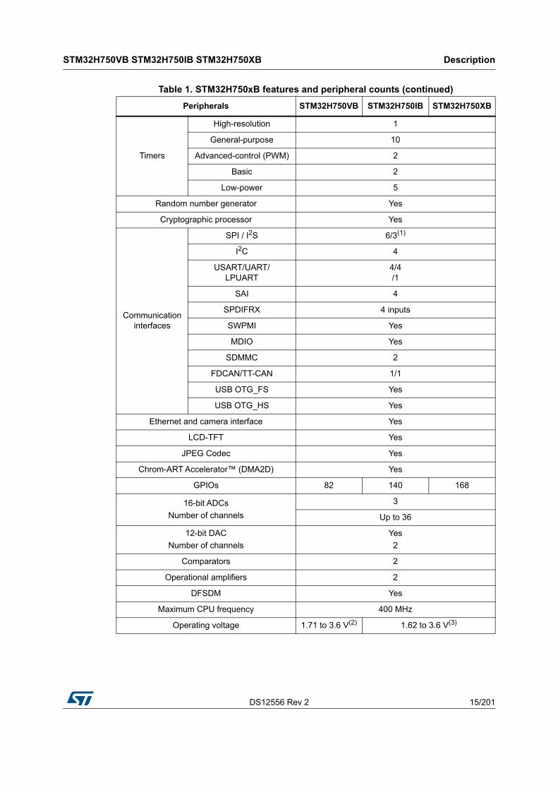
Refer to Table 1: STM32H750xB features and peripheral counts for the list of peripherals available on each part number.

Description STM32H750VB STM32H750IB STM32H750XB
14/201 DS12556 Rev 2
STM32H750xB devices operate in the –40 to +85 °C temperature range from a 1.62 to 3.6 V power supply. The supply voltage can drop down to 1.62 V by using an external power supervisor (see Section 3.5.2: Power supply supervisor) and connecting the PDR_ON pin to VSS. Otherwise the supply voltage must stay above 1.71 V with the embedded power voltage detector enabled.
Dedicated supply inputs for USB (OTG_FS and OTG_HS) are available on all packages except LQFP100 to allow a greater power supply choice.
A comprehensive set of power-saving modes allows the design of low-power applications.
STM32H750xB devices are offered in 3 packages ranging from 100 pins to 240 pins/balls. The set of included peripherals changes with the device chosen.
These features make STM32H750xB microcontrollers suitable for a wide range of applications:
• Motor drive and application control
• Medical equipment
• Industrial applications: PLC, inverters, circuit breakers
• Printers, and scanners
• Alarm systems, video intercom, and HVAC
• Home audio appliances
• Mobile applications, Internet of Things
• Wearable devices: smart watches.
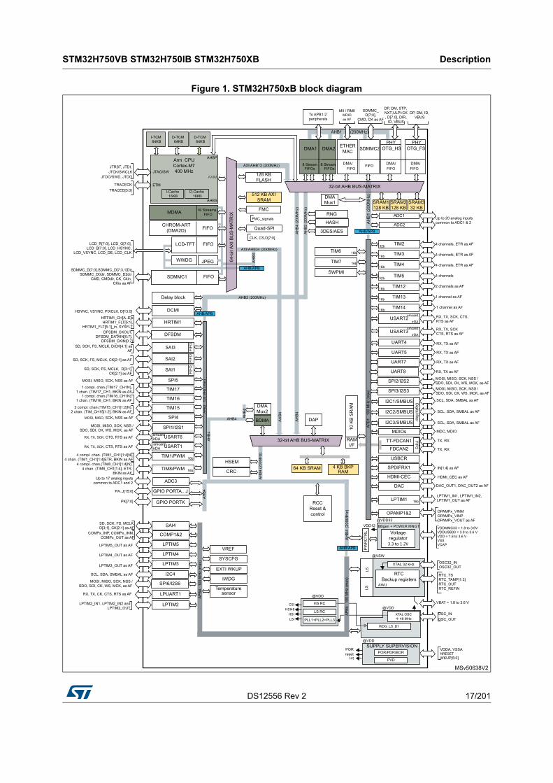
Figure 1 shows the general block diagram of the device family.
Table 1. STM32H750xB features and peripheral counts
Peripherals STM32H750VB STM32H750IB STM32H750XB
Flash memory in Kbytes 128
SRAM in Kbytes
SRAM mapped onto AXI bus
512
SRAM1 (D2 domain) 128
SRAM2 (D2 domain) 128
SRAM3 (D2 domain) 32
SRAM4 (D3 domain) 64
TCM RAM in Kbytes
ITCM RAM
(instruction)64
DTCM RAM (data) 128
Backup SRAM (Kbytes) 4
FMC Yes
Quad-SPI Yes
Ethernet Yes
DS12556 Rev 2 15/201
STM32H750VB STM32H750IB STM32H750XB Description
48
Timers
High-resolution 1
General-purpose 10
Advanced-control (PWM) 2
Basic 2
Low-power 5
Random number generator Yes
Cryptographic processor Yes
Communication interfaces
SPI / I2S 6/3(1)
I2C 4
USART/UART/LPUART
4/4/1
SAI 4
SPDIFRX 4 inputs
SWPMI Yes
MDIO Yes
SDMMC 2
FDCAN/TT-CAN 1/1
USB OTG_FS Yes
USB OTG_HS Yes
Ethernet and camera interface Yes
LCD-TFT Yes
JPEG Codec Yes
Chrom-ART Accelerator™ (DMA2D) Yes
GPIOs 82 140 168
16-bit ADCs
Number of channels
3
Up to 36
12-bit DAC
Number of channels
Yes
2
Comparators 2
Operational amplifiers 2
DFSDM Yes
Maximum CPU frequency 400 MHz
Operating voltage 1.71 to 3.6 V(2) 1.62 to 3.6 V(3)
Table 1. STM32H750xB features and peripheral counts (continued)
Peripherals STM32H750VB STM32H750IB STM32H750XB

Description STM32H750VB STM32H750IB STM32H750XB
16/201 DS12556 Rev 2
Operating temperaturesAmbient temperatures: –40 up to +85 °C(4)
Junction temperature: –40 to + 125 °C
Package LQFP100 UFBGA176+25 TFBGA240+25
1. The SPI1, SPI2 and SPI3 interfaces give the flexibility to work in an exclusive way in either the SPI mode or the I2S audio mode.
2. Since the LQFP100 package does not feature the PDR_ON pin (tied internally to VDD), the minimum VDD value for this package is 1.71 V.
3. VDD/VDDA can drop down to 1.62 V by using an external power supervisor (see Section 3.5.2: Power supply supervisor) and connecting PDR_ON pin to VSS. Otherwise the supply voltage must stay above 1.71 V with the embedded power voltage detector enabled.
4. The product junction temperature must be kept within the –40 to +125 °C temperature range.
Table 1. STM32H750xB features and peripheral counts (continued)
Peripherals STM32H750VB STM32H750IB STM32H750XB
DS12556 Rev 2 17/201
STM32H750VB STM32H750IB STM32H750XB Description
48
Figure 1. STM32H750xB block diagram
MSv50638V2
TT-FDCAN1
FDCAN2
I2C1/SMBUS
I2C2/SMBUS
I2C3/SMBUS
AXI/AHB12 (200MHz)
4 compl. chan. (TIM1_CH1[1:4]N),4 chan. (TIM1_CH1[1:4]ETR, BKIN as AF
AP
B1
30
MH
z
TX, RX
SCL, SDA, SMBAL as AF
AP
B1
100
MH
z (m
ax)
MDMA
PK[7:0]
4 compl. chan.(TIM8_CH1[1:4]N),4 chan. (TIM8_CH1[1:4], ETR,
BKIN as AF
RX, TX, SCK, CTS, RTS as AF
SCL, SDA, SMBAL as AF
SCL, SDA, SMBAL as AF
MOSI, MISO, SCK, NSS /SDO, SDI, CK, WS, MCK, as AF
TX, RX
RX, TX as AF
RX, TX as AF
RX, TX, SCKCTS, RTS as AF
RX, TX, SCK, CTS, RTS as AF
1 channel as AF
smcard
irDA
1 channel as AF
2 channels as AF
4 channels
4 channels, ETR as AF
4 channels, ETR as AF
4 channels, ETR as AF
RX, TX as AF
FIFOLCD-TFT
FIFOCHROM-ART
(DMA2D)
SD, SCK, FS, MCLK, D/CK[4:1] as AF FI
FO
LCD_R[7:0], LCD_G[7:0], LCD_B[7:0], LCD_HSYNC,
LCD_VSYNC, LCD_DE, LCD_CLK
CLK, CS,D[7:0]
64-b
it A
XI B
US
-MAT
RIX
HDMI_CEC as AF
IN[1:4] as AF
MDC, MDIO
AXIMAXIM
Arm CPUCortex-M7400 MHz
AHBP
AHBS
TRACECKTRACED[3:0]
JTRST, JTDI,JTCK/SWCLK
JTDO/SWD, JTDOJTAG/SW
ETM
I-Cache 16KB
D-Cache 16KB
I-TCM 64KB
D-TCM 64KB
16 StreamsFIFO
SDMMC1SDMMC_D[7:0],SDMMC_D[7:3,1]Dir
SDMMC_D0dir, SDMMC_D2dirCMD, CMDdir, CK, Ckin,
CKio as AF
FIFO
DMA1
FIFOs8 Stream
DMA2
FIFOs
ETHERMAC
FIFO
SDMMC2
FIFO
OTG_HS
FIFO
OTG_FS
FIFO
SRAM1128 KB
8 Stream
FMC_signals
DMA/ DMA/ DMA/
PHY PHY
MII / RMII MDIO as AF
DP, DM, STP, NXT,ULPI:CK, D[7:0], DIR,
ID, VBUS
AH
B1
(200
MH
z)
ADC1
DAC_OUT1, DAC_OUT2 as AF
16b
AXI/AHB34 (200MHz)
JPEGWWDG
AH
B2
(200
MH
z)
AHB2 (200MHz)
PA..J[15:0]
HSYNC, VSYNC, PIXCLK, D[13:0]
SAI3
MOSI, MISO, SCK, NSS as AF
MOSI, MISO, SCK, NSS as AF
smcardirDA 32-bit AHB BUS-MATRIX
AH
B4
(200
MH
z)
BDMA
DMAMux2
Up to 20 analog inputs common to ADC1 & 2
HSEM
AH
B4
(200
MH
z)
AH
B3
AH
B4
AH
B4
AH
B4
AHB4
AH
B4
VDDA, VSSANRESETWKUP[5:0]
@VDD
RCC Reset & control
OSC32_INOSC32_OUT
VBAT = 1.8 to 3.6 V
AWU
VDD12 BBgen + POWER MNGT
LSLS
OSC_INOSC_OUT
RTC_TSRTC_TAMP[1:3]RTC_OUTRTC_REFIN
VDDMMC33 = 1.8 to 3.6VVDDUSB33 = 3.0 to 3.6 VVDD = 1.8 to 3.6 VVSSVCAP
@VDD
@VDD33
@VSW
PW
RC
TRL
AH
B4
(200
MH
z)
SUPPLY SUPERVISION
Int
POR reset
@VDD
WDG_LS_D1
LPTIM1_IN1, LPTIM1_IN2,LPTIM1_OUT as AF
OPAMPx_VINMOPAMPx_VINPOPAMPx_VOUT as AF
HRTIM1_CH[A..E]xHRTIM1_FLT[5:1],
HRTIM1_FLT[5:1]_in, SYSFLTDFSDM_CKOUT,
DFSDM_DATAIN[0:7],DFSDM_CKIN[0:7]
2 compl. chan.(TIM15_CH1[1:2]N),2 chan. (TIM_CH15[1:2], BKIN as AF
1 compl. chan.(TIM16_CH1N),1 chan. (TIM16_CH1, BKIN as AF
1 compl. chan.(TIM17_CH1N),1 chan. (TIM17_CH1, BKIN as AF
SDMMC_ D[7:0],
CMD, CK as AF
Up to 17 analog inputs common to ADC1 and 2
SD, SCK, FS, MCLK, D[3;1], CK[2:1] as AF
SCL, SDA, SMBAL as AF
COMPx_INP, COMPx_INM, COMPx_OUT as AF
LPTIM5_OUT as AF
D-TCM 64KB
AHB/APB
Quad-SPI
128 KB FLASH
512 KB AXI SRAM
FMC
Delay block
DCMIAHB/APB
HRTIM1
DFSDM
SD, SCK, FS, MCLK, CK[2:1] as AF FIFOSAI2
SD, SCK, FS, MCLK, D[3:1], CK[2:1] as AF FI
FOSAI1
SPI5
TIM17
TIM16
TIM15
SPI4
MOSI, MISO, SCK, NSS /SDO, SDI, CK, WS, MCK, as AF SPI1/I2S1
USART6
RX, TX, SCK, CTS, RTS as AF irDA USART1
TIM1/PWM 16b
TIM8/PWM 16b
AP
B2
100
MH
z (m
ax)
ADC3
GPIO PORTA.. J
GPIO PORTK
SAI4
COMP1&2
LPTIM5
LPTIM4_OUT as AF LPTIM4
LPTIM3_OUT as AF LPTIM3
I2C4MOSI, MISO, SCK, NSS /
SDO, SDI, CK, WS, MCK, as AF SPI6/I2S6
RX, TX, CK, CTS, RTS as AF LPUART1
LPTIM2
VREF
SYSCFG
EXTI WKUP
CRC
DAP
RNG
DMAMux1
To APB1-2 peripherals
SRAM2128 KB
SRAM332 KB
ADC2AHB/APB
TIM6 16b
TIM7 16b
SWPMI
TIM232b
TIM316b
TIM416b
TIM532b
TIM1216b
TIM1316b
TIM1416b
USART2
smcard
irDAUSART3
UART4
UART5
UART7
RX, TX as AFUART8
SPI2/I2S2MOSI, MISO, SCK, NSS /SDO, SDI, CK, WS, MCK, as AFSPI3/I2S3
Digital filter
MDIOs
FIFO
10 K
B S
RA
M
RAM I/F
USBCR
SPDIFRX1
HDMI-CEC
DAC
LPTIM1
OPAMP1&2
AHB/APB
XTAL 32 kHz
RTCBackup registers
XTAL OSC4- 48 MHz
HS RC
LS RC
PLL1+PLL2+PLL3
POR/PDR/BOR
PVD
smcard
Voltage regulator
3.3 to 1.2V
LSIHSI
CSIHSI48
LPTIM2_IN1, LPTIM2_IN2 and LPTIM2_OUT
AHB1 (200MHz)
DP, DM, ID, VBUS
64 KB SRAM 4 KB BKP RAM
AH
B4
32-bit AHB BUS-MATRIX
AP
B4
100
MH
z (m
ax)
AP
B4
100
MH
z (m
ax)
AP
B4
100
MH
z (m
ax)IWDG
Temperature sensor
HASH
3DES/AES
Functional overview STM32H750VB STM32H750IB STM32H750XB
18/201 DS12556 Rev 2
3 Functional overview
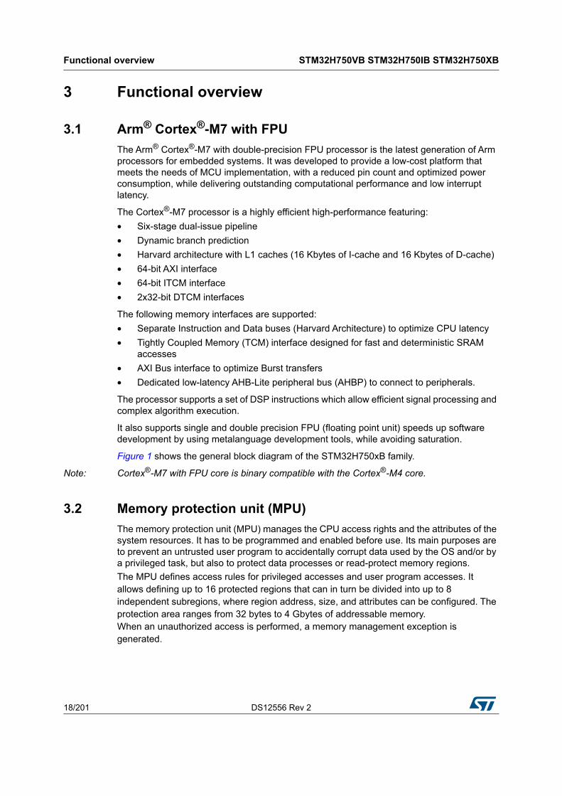
3.1 Arm® Cortex®-M7 with FPU
The Arm® Cortex®-M7 with double-precision FPU processor is the latest generation of Arm processors for embedded systems. It was developed to provide a low-cost platform that meets the needs of MCU implementation, with a reduced pin count and optimized power consumption, while delivering outstanding computational performance and low interrupt latency.
The Cortex®-M7 processor is a highly efficient high-performance featuring:
• Six-stage dual-issue pipeline
• Dynamic branch prediction
• Harvard architecture with L1 caches (16 Kbytes of I-cache and 16 Kbytes of D-cache)
• 64-bit AXI interface
• 64-bit ITCM interface
• 2x32-bit DTCM interfaces
The following memory interfaces are supported:
• Separate Instruction and Data buses (Harvard Architecture) to optimize CPU latency
• Tightly Coupled Memory (TCM) interface designed for fast and deterministic SRAM accesses
• AXI Bus interface to optimize Burst transfers
• Dedicated low-latency AHB-Lite peripheral bus (AHBP) to connect to peripherals.
The processor supports a set of DSP instructions which allow efficient signal processing and complex algorithm execution.
It also supports single and double precision FPU (floating point unit) speeds up software development by using metalanguage development tools, while avoiding saturation.
Figure 1 shows the general block diagram of the STM32H750xB family.
Note: Cortex®-M7 with FPU core is binary compatible with the Cortex®-M4 core.
3.2 Memory protection unit (MPU)
The memory protection unit (MPU) manages the CPU access rights and the attributes of the system resources. It has to be programmed and enabled before use. Its main purposes are to prevent an untrusted user program to accidentally corrupt data used by the OS and/or by a privileged task, but also to protect data processes or read-protect memory regions.
The MPU defines access rules for privileged accesses and user program accesses. It allows defining up to 16 protected regions that can in turn be divided into up to 8 independent subregions, where region address, size, and attributes can be configured. The protection area ranges from 32 bytes to 4 Gbytes of addressable memory.When an unauthorized access is performed, a memory management exception is generated.
DS12556 Rev 2 19/201
STM32H750VB STM32H750IB STM32H750XB Functional overview
48
3.3 Memories
3.3.1 Embedded Flash memory
The STM32H750xB devices embed 128 Kbytes of Flash memory that can be used for storing programs and data.
The Flash memory is organized as follows:
• 128 Kbytes of user Flash memory containing 128 Kbytes of System Flash memory from which the device can boot
• 2 Kbytes (64 Flash words) of user option bytes for user configuration
3.3.2 Secure access mode
In addition to other typical memory protection mechanism (RDP, PCROP), STM32H750xB devices introduce the Secure access mode, a new enhanced security feature. This mode allows developing user-defined secure services by ensuring, on the one hand code and data protection and on the other hand code safe execution.
Two types of secure services are available:
• STMicroelectronics Root Secure Services:
These services are embedded in System memory. They provide a secure solution for firmware and third-party modules installation. These services rely on cryptographic algorithms based on a device unique private key.
• User-defined secure services:
These services are embedded in user Flash memory. Examples of user secure services are proprietary user firmware update solution, secure Flash integrity check or any other sensitive applications that require a high level of protection.
The secure firmware is embedded in specific user Flash memory areas configured through option bytes.
Secure services are executed just after a reset and preempt all other applications to guarantee protected and safe execution. Once executed, the corresponding code and data are no more accessible.
The above secure services are available only for Cortex®-M7 core operating in Secure access mode. The other masters cannot access the option bytes involved in Secure access mode settings or the Flash secured areas.
Functional overview STM32H750VB STM32H750IB STM32H750XB
20/201 DS12556 Rev 2
3.3.3 Embedded SRAM
All devices feature:
• 512 Kbytes of AXI-SRAM mapped onto AXI bus on D1 domain.
• SRAM1 mapped on D2 domain: 128 Kbytes
• SRAM2 mapped on D2 domain: 128 Kbytes
• SRAM3 mapped on D2 domain: 32 Kbytes
• SRAM4 mapped on D3 domain: 64 Kbytes
• 4 Kbytes of backup SRAM
The content of this area is protected against possible unwanted write accesses, and is retained in Standby or VBAT mode.
• RAM mapped to TCM interface (ITCM and DTCM):
Both ITCM and DTCM RAMs are 0 wait state memories. either They can be accessed either from the CPU or the MDMA (even in Sleep mode) through a specific AHB slave of the CPU(AHBP):
– 64 Kbytes of ITCM-RAM (instruction RAM)
This RAM is connected to ITCM 64-bit interface designed for execution of critical real-times routines by the CPU.
– 128 Kbytes of DTCM-RAM (2x 64-Kbyte DTCM-RAMs on 2x32-bit DTCM ports)
The DTCM-RAM could be used for critical real-time data, such as interrupt service routines or stack/heap memory. Both DTCM-RAMs can be used in parallel (for load/store operations) thanks to the Cortex®-M7 dual issue capability.
The MDMA can be used to load code or data in ITCM or DTCM RAMs.
Error code correction (ECC)
Over the product lifetime, and/or due to external events such as radiations, invalid bits in memories may occur. They can be detected and corrected by ECC. This is an expected behavior that has to be managed at final-application software level in order to ensure data integrity through ECC algorithms implementation.
SRAM data are protected by ECC:
• 7 ECC bits are added per 32-bit word.
• 8 ECC bits are added per 64-bit word for AXI-SRAM and ITCM-RAM.
The ECC mechanism is based on the SECDED algorithm. It supports single-error correction and double-error detection.
3.4 Boot modes
At startup, the boot memory space is selected by the BOOT pin and BOOT_ADDx option bytes, allowing to program any boot memory address from 0x0000 0000 to 0x3FFF FFFF which includes:
• All Flash address space
• All RAM address space: ITCM, DTCM RAMs and SRAMs
• The System memory bootloader

DS12556 Rev 2 21/201
STM32H750VB STM32H750IB STM32H750XB Functional overview
48
The boot loader is located in non-user System memory. It is used to reprogram the Flash memory through a serial interface (USART, I2C, SPI, USB-DFU). Refer to STM32 microcontroller System memory Boot mode application note (AN2606) for details.
3.5 Power supply management
3.5.1 Power supply scheme
STM32H750xB power supply voltages are the following:
• VDD = 1.62 to 3.6 V: external power supply for I/Os, provided externally through VDD
pins.
• VDDLDO = 1.62 to 3.6 V: supply voltage for the internal regulator supplying VCORE
• VDDA = 1.62 to 3.6 V: external analog power supplies for ADC, DAC, COMP and OPAMP.
• VDD33USB and VDD50USB:
VDD50USB can be supplied through the USB cable to generate the VDD33USB via the USB internal regulator. This allows supporting a VDD supply different from 3.3 V.
The USB regulator can be bypassed to supply directly VDD33USB if VDD = 3.3 V.
• VBAT = 1.2 to 3.6 V: power supply for the VSW domain when VDD is not present.
• VCAP: VCORE supply voltage, which values depend on voltage scaling (0.7 V, 0.9 V, 1.0 V, 1.1 V or 1.2 V). They are configured through VOS bits in PWR_D3CR register. The VCORE domain is split into the following power domains that can be independently switch off.
– D1 domain containing some peripherals and the Cortex®-M7 core.
– D2 domain containing a large part of the peripherals.
– D3 domain containing some peripherals and the system control.
During power-up and power-down phases, the following power sequence requirements must be respected (see Figure 2):
• When VDD is below 1 V, other power supplies (VDDA, VDD33USB, VDD50USB) must remain below VDD + 300 mV.
• When VDD is above 1 V, all power supplies are independent.
During the power-down phase, VDD can temporarily become lower than other supplies only if the energy provided to the microcontroller remains below 1 mJ. This allows external decoupling capacitors to be discharged with different time constants during the power-down transient phase.

Functional overview STM32H750VB STM32H750IB STM32H750XB
22/201 DS12556 Rev 2
Figure 2. Power-up/power-down sequence
1. VDDx refers to any power supply among VDDA, VDD33USB, VDD50USB.
3.5.2 Power supply supervisor
The devices have an integrated power-on reset (POR)/ power-down reset (PDR) circuitry coupled with a Brownout reset (BOR) circuitry:
• Power-on reset (POR)
The POR supervisor monitors VDD power supply and compares it to a fixed threshold. The devices remain in Reset mode when VDD is below this threshold,
• Power-down reset (PDR)
The PDR supervisor monitors VDD power supply. A reset is generated when VDD drops below a fixed threshold.
The PDR supervisor can be enabled/disabled through PDR_ON pin.
• Brownout reset (BOR)
The BOR supervisor monitors VDD power supply. Three BOR thresholds (from 2.1 to 2.7 V) can be configured through option bytes. A reset is generated when VDD drops below this threshold.
MSv47490V1
0.3
1
VBOR0
3.6
Operating modePower-on Power-down time
V
VDDX(1)
VDD
Invalid supply area VDDX < VDD + 300 mV VDDX independent from VDD
DS12556 Rev 2 23/201
STM32H750VB STM32H750IB STM32H750XB Functional overview
48
3.5.3 Voltage regulator
The same voltage regulator supplies the 3 power domains (D1, D2 and D3). D1 and D2 can be independently switched off.
Voltage regulator output can be adjusted according to application needs through 5 power supply levels:
• Run mode (VOS1 to VOS3)
– Scale 1: high performance
– Scale 2: medium performance and consumption
– Scale 3: optimized performance and low-power consumption
• Stop mode (SVOS3 to SVOS5)
– Scale 3: peripheral with wakeup from Stop mode capabilities (UART, SPI, I2C, LPTIM) are operational
– Scale 4 and 5 where the peripheral with wakeup from Stop mode is disabled
The peripheral functionality is disabled but wakeup from Stop mode is possible through GPIO or asynchronous interrupt.
3.6 Low-power strategy
There are several ways to reduce power consumption on STM32H750xB:• Decrease dynamic power consumption by slowing down the system clocks even in
Run mode and individually clock gating the peripherals that are not used.
• Save power consumption when the CPU is idle, by selecting among the available low-power mode according to the user application needs. This allows achieving the best compromise between short startup time, low-power consumption, as well as available wakeup sources.
The devices feature several low-power modes:
• CSleep (CPU clock stopped)
• CStop (CPU sub-system clock stopped)
• DStop (Domain bus matrix clock stopped)
• Stop (System clock stopped)
• DStandby (Domain powered down)
• Standby (System powered down)
CSleep and CStop low-power modes are entered by the MCU when executing the WFI (Wait for Interrupt) or WFE (Wait for Event) instructions, or when the SLEEPONEXIT bit of the Cortex®-Mx core is set after returning from an interrupt service routine.
A domain can enter low-power mode (DStop or DStandby) when the processor, its subsystem and the peripherals allocated in the domain enter low-power mode.
If part of the domain is not in low-power mode, the domain remains in the current mode.
Finally the system can enter Stop or Standby when all EXTI wakeup sources are cleared and the power domains are in DStop or DStandby mode.

Functional overview STM32H750VB STM32H750IB STM32H750XB
24/201 DS12556 Rev 2
3.7 Reset and clock controller (RCC)
The clock and reset controller is located in D3 domain. The RCC manages the generation of all the clocks, as well as the clock gating and the control of the system and peripheral resets. It provides a high flexibility in the choice of clock sources and allows to apply clock ratios to improve the power consumption. In addition, on some communication peripherals that are capable to work with two different clock domains (either a bus interface clock or a kernel peripheral clock), the system frequency can be changed without modifying the baudrate.
3.7.1 Clock management
The devices embed four internal oscillators, two oscillators with external crystal or resonator, two internal oscillators with fast startup time and three PLLs.
The RCC receives the following clock source inputs:
• Internal oscillators:
– 64 MHz HSI clock
– 48 MHz RC oscillator
– 4 MHz CSI clock
– 32 kHz LSI clock
• External oscillators:
– 4-48 MHz HSE clock
– 32.768 kHz LSE clock
The RCC provides three PLLs: one for system clock, two for kernel clocks.
The system starts on the HSI clock. The user application can then select the clock configuration.
Table 2. System vs domain low-power mode
System power modeD1 domain power
modeD2 domain power
modeD3 domain power
mode
Run DRun/DStop/DStandby DRun/DStop/DStandby DRun
Stop DStop/DStandby DStop/DStandby DStop
Standby DStandby DStandby DStandby
DS12556 Rev 2 25/201
STM32H750VB STM32H750IB STM32H750XB Functional overview
48
3.7.2 System reset sources
Power-on reset initializes all registers while system reset reinitializes the system except for the debug, part of the RCC and power controller status registers, as well as the backup power domain.
A system reset is generated in the following cases:
• Power-on reset (pwr_por_rst)
• Brownout reset
• Low level on NRST pin (external reset)
• Window watchdog
• Independent watchdog
• Software reset
• Low-power mode security reset
• Exit from Standby
3.8 General-purpose input/outputs (GPIOs)
Each of the GPIO pins can be configured by software as output (push-pull or open-drain, with or without pull-up or pull-down), as input (floating, with or without pull-up or pull-down) or as peripheral alternate function. Most of the GPIO pins are shared with digital or analog alternate functions. All GPIOs are high-current-capable and have speed selection to better manage internal noise, power consumption and electromagnetic emission.
After reset, all GPIOs (except debug pins) are in Analog mode to reduce power consumption (refer to GPIOs register reset values in the device reference manual).
The I/O configuration can be locked if needed by following a specific sequence in order to avoid spurious writing to the I/Os registers.
3.9 Bus-interconnect matrix
The devices feature an AXI bus matrix, two AHB bus matrices and bus bridges that allow interconnecting bus masters with bus slaves (see Figure 3).
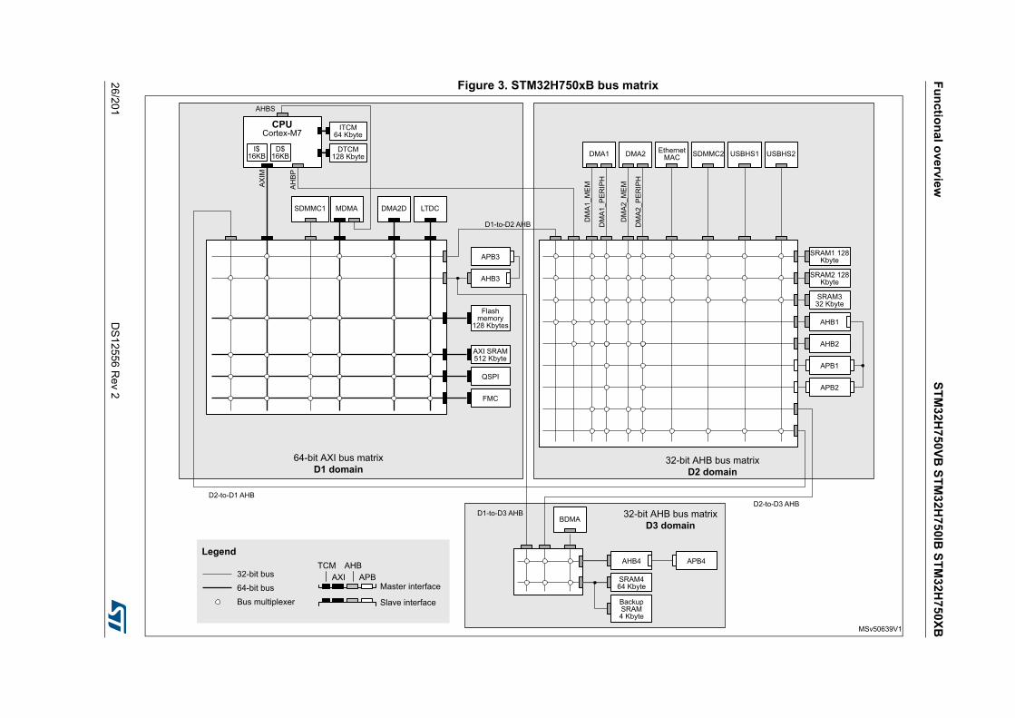
Fu
nctio
nal o
verview
ST
M3
2H
750
VB
ST
M3
2H75
0IB S
TM
32H
75
0XB
26/20
1D
S12
556 Re
v 2
Figure 3. STM32H750xB bus matrix
MSv50639V1
AX
IM
DMA2 EthernetMAC SDMMC2DMA1 USBHS1 USBHS2
APB1
SDMMC1 MDMA DMA2D LTDC
BDMA
APB4
Cortex-M7
I$16KB
D$16KB
AH
BP
DM
A1_
ME
M
DM
A1_
PE
RIP
H
DM
A2_
ME
M
DM
A2_
PE
RIP
H
APB3
32-bit AHB bus matrixD2 domain
64-bit AXI bus matrixD1 domain
32-bit AHB bus matrixD3 domain
DTCM128 Kbyte
ITCM64 Kbyte
Flash memory
128 Kbytes
AXI SRAM512 Kbyte
QSPI
FMC
SRAM1 128 Kbyte
SRAM2 128 Kbyte
SRAM332 Kbyte
AHB1
AHB2
AHB4
SRAM464 Kbyte
Backup SRAM4 Kbyte
AHBS
CPU
D2-to-D1 AHBD2-to-D3 AHB
D1-to-D2 AHB
D1-to-D3 AHB
32-bit bus64-bit busBus multiplexer
Legend
Master interface
Slave interface
AHB3
AXIAHB
APB
APB2
TCM
DS12556 Rev 2 27/201
STM32H750VB STM32H750IB STM32H750XB Functional overview
48
3.10 DMA controllers
. The devices feature four DMA instances to unload CPU activity:
• A master direct memory access (MDMA)
The MDMA is a high-speed DMA controller, which is in charge of all types of memory transfers (peripheral to memory, memory to memory, memory to peripheral), without any CPU action. It features a master AXI interface and a dedicated AHB interface to access Cortex®-M7 TCM memories.
The MDMA is located in D1 domain. It is able to interface with the other DMA controllers located in D2 domain to extend the standard DMA capabilities, or can manage peripheral DMA requests directly.
Each of the 16 channels can perform single block transfers, repeated block transfers and linked list transfers.
• Two dual-port DMAs (DMA1, DMA2) located in D2 domain, with FIFO and request router capabilities.
• One basic DMA (BDMA) located in D3 domain, with request router capabilities.
The DMA request router could be considered as an extension of the DMA controller. It routes the DMA peripheral requests to the DMA controller itself. This allowing managing the DMA requests with a high flexibility, maximizing the number of DMA requests that run concurrently, as well as generating DMA requests from peripheral output trigger or DMA event.
3.11 Chrom-ART Accelerator™ (DMA2D)
The Chrom-Art Accelerator™ (DMA2D) is a graphical accelerator which offers advanced bit blitting, row data copy and pixel format conversion. It supports the following functions:
• Rectangle filling with a fixed color
• Rectangle copy
• Rectangle copy with pixel format conversion
• Rectangle composition with blending and pixel format conversion
Various image format coding are supported, from indirect 4bpp color mode up to 32bpp direct color. It embeds dedicated memory to store color lookup tables. The DMA2D also supports block based YCbCr to handle JPEG decoder output.
An interrupt can be generated when an operation is complete or at a programmed watermark.
All the operations are fully automatized and are running independently from the CPU or the DMAs.

Functional overview STM32H750VB STM32H750IB STM32H750XB
28/201 DS12556 Rev 2
3.12 Nested vectored interrupt controller (NVIC)
The devices embed a nested vectored interrupt controller which is able to manage 16 priority levels, and handle up to 150 maskable interrupt channels plus the 16 interrupt lines of the Cortex®-M7 with FPU core.
• Closely coupled NVIC gives low-latency interrupt processing
• Interrupt entry vector table address passed directly to the core
• Allows early processing of interrupts
• Processing of late arriving, higher-priority interrupts
• Support tail chaining
• Processor context automatically saved on interrupt entry, and restored on interrupt exit with no instruction overhead
This hardware block provides flexible interrupt management features with minimum interrupt latency.
3.13 Extended interrupt and event controller (EXTI)
The EXTI controller performs interrupt and event management. In addition, it can wake up the processor, power domains and/or D3 domain from Stop mode.
The EXTI handles up to 89 independent event/interrupt lines split as 28 configurable events and 61 direct events .
Configurable events have dedicated pending flags, active edge selection, and software trigger capable.
Direct events provide interrupts or events from peripherals having a status flag.
3.14 Cyclic redundancy check calculation unit (CRC)
The CRC (cyclic redundancy check) calculation unit is used to get a CRC code using a programmable polynomial.
Among other applications, CRC-based techniques are used to verify data transmission or storage integrity. In the scope of the EN/IEC 60335-1 standard, they offer a means of verifying the Flash memory integrity. The CRC calculation unit helps compute a signature of the software during runtime, to be compared with a reference signature generated at link-time and stored at a given memory location.

DS12556 Rev 2 29/201
STM32H750VB STM32H750IB STM32H750XB Functional overview
48
3.15 Flexible memory controller (FMC)
The FMC controller main features are the following:• Interface with static-memory mapped devices including:
– Static random access memory (SRAM)
– NOR Flash memory/OneNAND Flash memory
– PSRAM (4 memory banks)
– NAND Flash memory with ECC hardware to check up to 8 Kbytes of data
• Interface with synchronous DRAM (SDRAM/Mobile LPSDR SDRAM) memories
• 8-,16-,32-bit data bus width
• Independent Chip Select control for each memory bank
• Independent configuration for each memory bank
• Write FIFO
• Read FIFO for SDRAM controller
• The maximum FMC_CLK/FMC_SDCLK frequency for synchronous accesses is the FMC kernel clock divided by 2.
3.16 Quad-SPI memory interface (QUADSPI)
All devices embed a Quad-SPI memory interface, which is a specialized communication interface targeting Single, Dual or Quad-SPI Flash memories. It supports both single and double datarate operations.
It can operate in any of the following modes:
• Direct mode through registers
• External Flash status register polling mode
• Memory mapped mode.
Up to 256 Mbytes of external Flash memory can be mapped, and 8-, 16- and 32-bit data accesses are supported as well as code execution.
The opcode and the frame format are fully programmable.
3.17 Analog-to-digital converters (ADCs)
The STM32H750xB devices embed three analog-to-digital converters, which resolution can be configured to 16, 14, 12, 10 or 8 bits. The sampling rates are respectively 3.6 MSPS, 4 MSPS, 4.5 MSPS, 5 MSPS and 6 MSPS when the ADC frequency (fADC) is 36 MHz.
Each ADC shares up to 20 external channels, performing conversions in the Single-shot or Scan mode. In Scan mode, automatic conversion is performed on a selected group of analog inputs.
Additional logic functions embedded in the ADC interface allow:
• Simultaneous sample and hold
• Interleaved sample and hold
The ADC can be served by the DMA controller, thus allowing to automatically transfer ADC converted values to a destination location without any software action.
Functional overview STM32H750VB STM32H750IB STM32H750XB
30/201 DS12556 Rev 2
In addition, an analog watchdog feature can accurately monitor the converted voltage of one, some or all selected channels. An interrupt is generated when the converted voltage is outside the programmed thresholds.
To synchronize A/D conversion and timers, the ADCs could be triggered by any of TIM1, TIM2, TIM3, TIM4, TIM6, TIM8, TIM15, HRTIM1 and LPTIM1 timer.
3.18 Temperature sensor
STM32H750xB devices embed a temperature sensor that generates a voltage (VTS) that varies linearly with the temperature. This temperature sensor is internally connected to ADC3_IN18. The conversion range is between 1.7 V and 3.6 V. It can measure the device junction temperature ranging from − 40 to +125 °C.
The temperature sensor have a good linearity, but it has to be calibrated to obtain a good overall accuracy of the temperature measurement. As the temperature sensor offset varies from chip to chip due to process variation, the uncalibrated internal temperature sensor is suitable for applications that detect temperature changes only. To improve the accuracy of the temperature sensor measurement, each device is individually factory-calibrated by ST. The temperature sensor factory calibration data are stored by ST in the System memory area, which is accessible in Read-only mode.
3.19 VBAT operation
The VBAT power domain contains the RTC, the backup registers and the backup SRAM.
To optimize battery duration, this power domain is supplied by VDD when available or by the voltage applied on VBAT pin (when VDD supply is not present). VBAT power is switched when the PDR detects that VDD dropped below the PDR level.
The voltage on the VBAT pin could be provided by an external battery, a supercapacitor or directly by VDD, in which case, the VDD mode is not functional.
VBAT operation is activated when VDD is not present.
The VBAT pin supplies the RTC, the backup registers and the backup SRAM.
Note: When the microcontroller is supplied from VBAT, external interrupts and RTC alarm/events do not exit it from VBAT operation.
When PDR_ON pin is connected to VSS (Internal Reset OFF), the VBAT functionality is no more available and VBAT pin should be connected to VDD.
DS12556 Rev 2 31/201
STM32H750VB STM32H750IB STM32H750XB Functional overview
48
3.20 Digital-to-analog converters (DAC)
The two 12-bit buffered DAC channels can be used to convert two digital signals into two analog voltage signal outputs.
This dual digital Interface supports the following features:
• two DAC converters: one for each output channel
• 8-bit or 12-bit monotonic output
• left or right data alignment in 12-bit mode
• synchronized update capability
• noise-wave generation
• triangular-wave generation
• dual DAC channel independent or simultaneous conversions
• DMA capability for each channel including DMA underrun error detection
• external triggers for conversion
• input voltage reference VREF+ or internal VREFBUF reference.
The DAC channels are triggered through the timer update outputs that are also connected to different DMA streams.
3.21 Ultra-low-power comparators (COMP)
STM32H750xB devices embed two rail-to-rail comparators (COMP1 and COMP2). They feature programmable reference voltage (internal or external), hysteresis and speed (low speed for low-power) as well as selectable output polarity.
The reference voltage can be one of the following:
• An external I/O
• A DAC output channel
• An internal reference voltage or submultiple (1/4, 1/2, 3/4).
All comparators can wake up from Stop mode, generate interrupts and breaks for the timers, and be combined into a window comparator.
3.22 Operational amplifiers (OPAMP)
STM32H750xB devices embed two rail-to-rail operational amplifiers (OPAMP1 and OPAMP2) with external or internal follower routing and PGA capability.
The operational amplifier main features are:
• PGA with a non-inverting gain ranging of 2, 4, 8 or 16 or inverting gain ranging of -1, -3, -7 or -15
• One positive input connected to DAC
• Output connected to internal ADC
• Low input bias current down to 1 nA
• Low input offset voltage down to 1.5 mV
• Gain bandwidth up to 8 MHz

Functional overview STM32H750VB STM32H750IB STM32H750XB
32/201 DS12556 Rev 2
The devices embeds two operational amplifiers (OPAMP1 and OPAMP2) with two inputs and one output each. These three I/Os can be connected to the external pins, thus enabling any type of external interconnections. The operational amplifiers can be configured internally as a follower, as an amplifier with a non-inverting gain ranging from 2 to 16 or with inverting gain ranging from -1 to -15.
3.23 Digital filter for sigma-delta modulators (DFSDM)
The devices embed one DFSDM with 4 digital filters modules and 8 external input serial channels (transceivers) or alternately 8 internal parallel inputs support.
The DFSDM peripheral is dedicated to interface the external Σ∆ modulators to microcontroller and then to perform digital filtering of the received data streams (which represent analog value on Σ∆ modulators inputs). DFSDM can also interface PDM (Pulse Density Modulation) microphones and perform PDM to PCM conversion and filtering in hardware. DFSDM features optional parallel data stream inputs from internal ADC peripherals or microcontroller memory (through DMA/CPU transfers into DFSDM).
DFSDM transceivers support several serial interface formats (to support various Σ∆ modulators). DFSDM digital filter modules perform digital processing according user selected filter parameters with up to 24-bit final ADC resolution.
The DFSDM peripheral supports:
• 8 multiplexed input digital serial channels:
– configurable SPI interface to connect various SD modulator(s)
– configurable Manchester coded 1 wire interface support
– PDM (Pulse Density Modulation) microphone input support
– maximum input clock frequency up to 20 MHz (10 MHz for Manchester coding)
– clock output for SD modulator(s): 0..20 MHz
• alternative inputs from 8 internal digital parallel channels (up to 16 bit input resolution):
– internal sources: ADC data or memory data streams (DMA)
• 4 digital filter modules with adjustable digital signal processing:
– Sincx filter: filter order/type (1..5), oversampling ratio (up to 1..1024)
– integrator: oversampling ratio (1..256)
• up to 24-bit output data resolution, signed output data format
• automatic data offset correction (offset stored in register by user)
• continuous or single conversion
• start-of-conversion triggered by:
– software trigger
– internal timers
– external events
– start-of-conversion synchronously with first digital filter module (DFSDM0)
• analog watchdog feature:
– low value and high value data threshold registers
– dedicated configurable Sincx digital filter (order = 1..3, oversampling ratio = 1..32)
– input from final output data or from selected input digital serial channels
– continuous monitoring independently from standard conversion
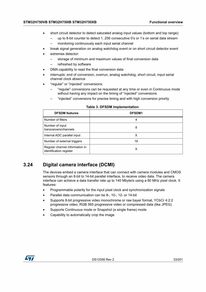
DS12556 Rev 2 33/201
STM32H750VB STM32H750IB STM32H750XB Functional overview
48
• short circuit detector to detect saturated analog input values (bottom and top range):
– up to 8-bit counter to detect 1..256 consecutive 0’s or 1’s on serial data stream
– monitoring continuously each input serial channel
• break signal generation on analog watchdog event or on short circuit detector event
• extremes detector:
– storage of minimum and maximum values of final conversion data
– refreshed by software
• DMA capability to read the final conversion data
• interrupts: end of conversion, overrun, analog watchdog, short circuit, input serial channel clock absence
• “regular” or “injected” conversions:
– “regular” conversions can be requested at any time or even in Continuous mode without having any impact on the timing of “injected” conversions
– “injected” conversions for precise timing and with high conversion priority
3.24 Digital camera interface (DCMI)
The devices embed a camera interface that can connect with camera modules and CMOS sensors through an 8-bit to 14-bit parallel interface, to receive video data. The camera interface can achieve a data transfer rate up to 140 Mbyte/s using a 80 MHz pixel clock. It features:
• Programmable polarity for the input pixel clock and synchronization signals
• Parallel data communication can be 8-, 10-, 12- or 14-bit
• Supports 8-bit progressive video monochrome or raw bayer format, YCbCr 4:2:2 progressive video, RGB 565 progressive video or compressed data (like JPEG)
• Supports Continuous mode or Snapshot (a single frame) mode
• Capability to automatically crop the image
Table 3. DFSDM implementation
DFSDM features DFSDM1
Number of filters 4
Number of input transceivers/channels
8
Internal ADC parallel input X
Number of external triggers 16
Regular channel information in identification register
X
Functional overview STM32H750VB STM32H750IB STM32H750XB
34/201 DS12556 Rev 2
3.25 LCD-TFT controller
The LCD-TFT display controller provides a 24-bit parallel digital RGB (Red, Green, Blue) and delivers all signals to interface directly to a broad range of LCD and TFT panels up to XGA (1024x768) resolution with the following features:
• 2 display layers with dedicated FIFO (64x64-bit)
• Color Look-Up table (CLUT) up to 256 colors (256x24-bit) per layer
• Up to 8 input color formats selectable per layer
• Flexible blending between two layers using alpha value (per pixel or constant)
• Flexible programmable parameters for each layer
• Color keying (transparency color)
• Up to 4 programmable interrupt events
• AXI master interface with burst of 16 words
3.26 JPEG Codec (JPEG)
The JPEG Codec can encode and decode a JPEG stream as defined in the ISO/IEC 10918-1 specification. It provides an fast and simple hardware compressor and decompressor of JPEG images with full management of JPEG headers.
The JPEG codec main features are as follows:
• 8-bit/channel pixel depths
• Single clock per pixel encoding and decoding
• Support for JPEG header generation and parsing
• Up to four programmable quantization tables
• Fully programmable Huffman tables (two AC and two DC)
• Fully programmable minimum coded unit (MCU)
• Encode/decode support (non simultaneous)
• Single clock Huffman coding and decoding
• Two-channel interface: Pixel/Compress In, Pixel/Compressed Out
• Support for single greyscale component
• Ability to enable/disable header processing
• Fully synchronous design
• Configuration for High-speed decode mode
3.27 Random number generator (RNG)
All devices embed an RNG that delivers 32-bit random numbers generated by an integrated analog circuit.
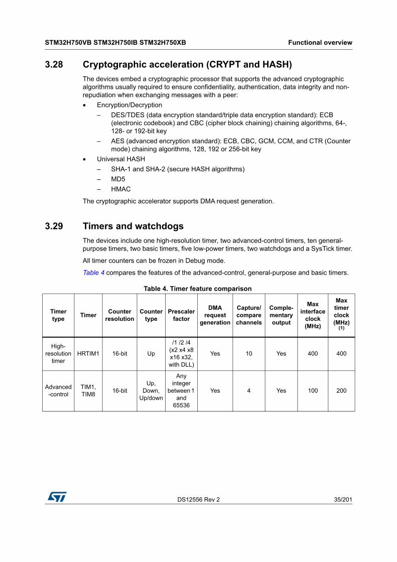
DS12556 Rev 2 35/201
STM32H750VB STM32H750IB STM32H750XB Functional overview
48
3.28 Cryptographic acceleration (CRYPT and HASH)
The devices embed a cryptographic processor that supports the advanced cryptographic algorithms usually required to ensure confidentiality, authentication, data integrity and non-repudiation when exchanging messages with a peer:
• Encryption/Decryption
– DES/TDES (data encryption standard/triple data encryption standard): ECB (electronic codebook) and CBC (cipher block chaining) chaining algorithms, 64-, 128- or 192-bit key
– AES (advanced encryption standard): ECB, CBC, GCM, CCM, and CTR (Counter mode) chaining algorithms, 128, 192 or 256-bit key
• Universal HASH
– SHA-1 and SHA-2 (secure HASH algorithms)
– MD5
– HMAC
The cryptographic accelerator supports DMA request generation.
3.29 Timers and watchdogs
The devices include one high-resolution timer, two advanced-control timers, ten general-purpose timers, two basic timers, five low-power timers, two watchdogs and a SysTick timer.
All timer counters can be frozen in Debug mode.
Table 4 compares the features of the advanced-control, general-purpose and basic timers.
Table 4. Timer feature comparison
Timer type
TimerCounter
resolutionCounter
typePrescaler
factor
DMA request
generation
Capture/compare channels
Comple-mentary output
Max interface
clock (MHz)
Max timer clock (MHz)
(1)
High-resolution
timerHRTIM1 16-bit Up
/1 /2 /4(x2 x4 x8 x16 x32, with DLL)
Yes 10 Yes 400 400
Advanced-control
TIM1, TIM8
16-bitUp,
Down, Up/down
Any integer
between 1 and
65536
Yes 4 Yes 100 200

Functional overview STM32H750VB STM32H750IB STM32H750XB
36/201 DS12556 Rev 2
General purpose
TIM2, TIM5
32-bitUp,
Down, Up/down
Any integer
between 1 and
65536
Yes 4 No 100 200
TIM3, TIM4
16-bitUp,
Down, Up/down
Any integer
between 1 and
65536
Yes 4 No 100 200
TIM12 16-bit Up
Any integer
between 1 and
65536
No 2 No 100 200
TIM13, TIM14
16-bit Up
Any integer
between 1 and
65536
No 1 No 100 200
TIM15 16-bit Up
Any integer
between 1 and
65536
Yes 2 1 100 200
TIM16, TIM17
16-bit Up
Any integer
between 1 and
65536
Yes 1 1 100 200
BasicTIM6, TIM7
16-bit Up
Any integer
between 1 and
65536
Yes 0 No 100 200
Low-power timer
LPTIM1, LPTIM2, LPTIM3, LPTIM4, LPTIM5
16-bit Up1, 2, 4, 8, 16, 32, 64,
128No 0 No 100 200
1. The maximum timer clock is up to 400 MHz depending on TIMPRE bit in the RCC_CFGR register and D2PRE1/2 bits in RCC_D2CFGR register.
Table 4. Timer feature comparison (continued)
Timer type
TimerCounter
resolutionCounter
typePrescaler
factor
DMA request
generation
Capture/compare channels
Comple-mentary output
Max interface
clock (MHz)
Max timer clock (MHz)
(1)
DS12556 Rev 2 37/201
STM32H750VB STM32H750IB STM32H750XB Functional overview
48
3.29.1 High-resolution timer (HRTIM1)
The high-resolution timer (HRTIM1) allows generating digital signals with high-accuracy timings, such as PWM or phase-shifted pulses.
It consists of 6 timers, 1 master and 5 slaves, totaling 10 high-resolution outputs, which can be coupled by pairs for deadtime insertion. It also features 5 fault inputs for protection purposes and 10 inputs to handle external events such as current limitation, zero voltage or zero current switching.
The HRTIM1 timer is made of a digital kernel clocked at 400 MHz The high-resolution is available on the 10 outputs in all operating modes: variable duty cycle, variable frequency, and constant ON time.
The slave timers can be combined to control multiswitch complex converters or operate independently to manage multiple independent converters.
The waveforms are defined by a combination of user-defined timings and external events such as analog or digital feedbacks signals.
HRTIM1 timer includes options for blanking and filtering out spurious events or faults. It also offers specific modes and features to offload the CPU: DMA requests, Burst mode controller, Push-pull and Resonant mode.
It supports many topologies including LLC, Full bridge phase shifted, buck or boost converters, either in voltage or current mode, as well as lighting application (fluorescent or LED). It can also be used as a general purpose timer, for instance to achieve high-resolution PWM-emulated DAC.
Functional overview STM32H750VB STM32H750IB STM32H750XB
38/201 DS12556 Rev 2
3.29.2 Advanced-control timers (TIM1, TIM8)
The advanced-control timers (TIM1, TIM8) can be seen as three-phase PWM generators multiplexed on 6 channels. They have complementary PWM outputs with programmable inserted dead times. They can also be considered as complete general-purpose timers. Their 4 independent channels can be used for:
• Input capture
• Output compare
• PWM generation (Edge- or Center-aligned modes)
• One-pulse mode output
If configured as standard 16-bit timers, they have the same features as the general-purpose TIMx timers. If configured as 16-bit PWM generators, they have full modulation capability (0-100%).
The advanced-control timer can work together with the TIMx timers via the Timer Link feature for synchronization or event chaining.
TIM1 and TIM8 support independent DMA request generation.
3.29.3 General-purpose timers (TIMx)
There are ten synchronizable general-purpose timers embedded in the STM32H750xB devices (see Table 4 for differences).
• TIM2, TIM3, TIM4, TIM5
The devices include 4 full-featured general-purpose timers: TIM2, TIM3, TIM4 and TIM5. TIM2 and TIM5 are based on a 32-bit auto-reload up/downcounter and a 16-bit prescaler while TIM3 and TIM4 are based on a 16-bit auto-reload up/downcounter and a 16-bit prescaler. All timers feature 4 independent channels for input capture/output compare, PWM or One-pulse mode output. This gives up to 16 input capture/output compare/PWMs on the largest packages.
TIM2, TIM3, TIM4 and TIM5 general-purpose timers can work together, or with the other general-purpose timers and the advanced-control timers TIM1 and TIM8 via the Timer Link feature for synchronization or event chaining.
Any of these general-purpose timers can be used to generate PWM outputs.
TIM2, TIM3, TIM4, TIM5 all have independent DMA request generation. They are capable of handling quadrature (incremental) encoder signals and the digital outputs from 1 to 4 hall-effect sensors.
• TIM12, TIM13, TIM14, TIM15, TIM16, TIM17
These timers are based on a 16-bit auto-reload upcounter and a 16-bit prescaler. TIM13, TIM14, TIM16 and TIM17 feature one independent channel, whereas TIM12 and TIM15 have two independent channels for input capture/output compare, PWM or One-pulse mode output. They can be synchronized with the TIM2, TIM3, TIM4, TIM5 full-featured general-purpose timers or used as simple timebases.
DS12556 Rev 2 39/201
STM32H750VB STM32H750IB STM32H750XB Functional overview
48
3.29.4 Basic timers TIM6 and TIM7
These timers are mainly used for DAC trigger and waveform generation. They can also be used as a generic 16-bit time base.
TIM6 and TIM7 support independent DMA request generation.
3.29.5 Low-power timers (LPTIM1, LPTIM2, LPTIM3, LPTIM4, LPTIM5)
The low-power timers have an independent clock and is running also in Stop mode if it is clocked by LSE, LSI or an external clock. It is able to wakeup the devices from Stop mode.
This low-power timer supports the following features:
• 16-bit up counter with 16-bit autoreload register
• 16-bit compare register
• Configurable output: pulse, PWM
• Continuous / One-shot mode
• Selectable software / hardware input trigger
• Selectable clock source:
• Internal clock source: LSE, LSI, HSI or APB clock
• External clock source over LPTIM input (working even with no internal clock source running, used by the Pulse Counter Application)
• Programmable digital glitch filter
• Encoder mode
3.29.6 Independent watchdog
The independent watchdog is based on a 12-bit downcounter and 8-bit prescaler. It is clocked from an independent 32 kHz internal RC and as it operates independently from the main clock, it can operate in Stop and Standby modes. It can be used either as a watchdog to reset the device when a problem occurs, or as a free-running timer for application timeout management. It is hardware- or software-configurable through the option bytes.
3.29.7 Window watchdog
The window watchdog is based on a 7-bit downcounter that can be set as free-running. It can be used as a watchdog to reset the device when a problem occurs. It is clocked from the main clock. It has an early warning interrupt capability and the counter can be frozen in Debug mode.
3.29.8 SysTick timer
This timer is dedicated to real-time operating systems, but could also be used as a standard downcounter. It features:
• A 24-bit downcounter
• Autoreload capability
• Maskable system interrupt generation when the counter reaches 0
• Programmable clock source.
Functional overview STM32H750VB STM32H750IB STM32H750XB
40/201 DS12556 Rev 2
3.30 Real-time clock (RTC), backup SRAM and backup registers
The RTC is an independent BCD timer/counter. It supports the following features:
• Calendar with subsecond, seconds, minutes, hours (12 or 24 format), week day, date, month, year, in BCD (binary-coded decimal) format.
• Automatic correction for 28, 29 (leap year), 30, and 31 days of the month.
• Two programmable alarms.
• On-the-fly correction from 1 to 32767 RTC clock pulses. This can be used to synchronize it with a master clock.
• Reference clock detection: a more precise second source clock (50 or 60 Hz) can be used to enhance the calendar precision.
• Digital calibration circuit with 0.95 ppm resolution, to compensate for quartz crystal inaccuracy.
• Three anti-tamper detection pins with programmable filter.
• Timestamp feature which can be used to save the calendar content. This function can be triggered by an event on the timestamp pin, or by a tamper event, or by a switch to VBAT mode.
• 17-bit auto-reload wakeup timer (WUT) for periodic events with programmable resolution and period.
The RTC and the 32 backup registers are supplied through a switch that takes power either from the VDD supply when present or from the VBAT pin.
The backup registers are 32-bit registers used to store 128 bytes of user application data when VDD power is not present. They are not reset by a system or power reset, or when the device wakes up from Standby mode.
The RTC clock sources can be:
• A 32.768 kHz external crystal (LSE)
• An external resonator or oscillator (LSE)
• The internal low-power RC oscillator (LSI, with typical frequency of 32 kHz)
• The high-speed external clock (HSE) divided by 32.
The RTC is functional in VBAT mode and in all low-power modes when it is clocked by the LSE. When clocked by the LSI, the RTC is not functional in VBAT mode, but is functional in all low-power modes.
All RTC events (Alarm, Wakeup Timer, Timestamp or Tamper) can generate an interrupt and wakeup the device from the low-power modes.

DS12556 Rev 2 41/201
STM32H750VB STM32H750IB STM32H750XB Functional overview
48
3.31 Inter-integrated circuit interface (I2C)
STM32H750xB devices embed four I2C interfaces.
The I2C bus interface handles communications between the microcontroller and the serial I2C bus. It controls all I2C bus-specific sequencing, protocol, arbitration and timing.
The I2C peripheral supports:
• I2C-bus specification and user manual rev. 5 compatibility:
– Slave and Master modes, multimaster capability
– Standard-mode (Sm), with a bitrate up to 100 kbit/s
– Fast-mode (Fm), with a bitrate up to 400 kbit/s
– Fast-mode Plus (Fm+), with a bitrate up to 1 Mbit/s and 20 mA output drive I/Os
– 7-bit and 10-bit addressing mode, multiple 7-bit slave addresses
– Programmable setup and hold times
– Optional clock stretching
• System Management Bus (SMBus) specification rev 2.0 compatibility:
– Hardware PEC (Packet Error Checking) generation and verification with ACK control
– Address resolution protocol (ARP) support
– SMBus alert
• Power System Management Protocol (PMBusTM) specification rev 1.1 compatibility
• Independent clock: a choice of independent clock sources allowing the I2C communication speed to be independent from the PCLK reprogramming.
• Wakeup from Stop mode on address match
• Programmable analog and digital noise filters
• 1-byte buffer with DMA capability
3.32 Universal synchronous/asynchronous receiver transmitter (USART)
STM32H750xB devices have four embedded universal synchronous receiver transmitters (USART1, USART2, USART3 and USART6) and four universal asynchronous receiver transmitters (UART4, UART5, UART7 and UART8). Refer to Table 5 for a summary of USARTx and UARTx features.
These interfaces provide asynchronous communication, IrDA SIR ENDEC support, multiprocessor communication mode, single-wire Half-duplex communication mode and have LIN Master/Slave capability. They provide hardware management of the CTS and RTS signals, and RS485 Driver Enable. They are able to communicate at speeds of up to 12.5 Mbit/s.
USART1, USART2, USART3 and USART6 also provide Smartcard mode (ISO 7816 compliant) and SPI-like communication capability.
The USARTs embed a Transmit FIFO (TXFIFO) and a Receive FIFO (RXFIFO). FIFO mode is enabled by software and is disabled by default.

Functional overview STM32H750VB STM32H750IB STM32H750XB
42/201 DS12556 Rev 2
All USART have a clock domain independent from the CPU clock, allowing the USARTx to wake up the MCU from Stop mode.The wakeup from Stop mode is programmable and can be done on:
• Start bit detection
• Any received data frame
• A specific programmed data frame
• Specific TXFIFO/RXFIFO status when FIFO mode is enabled.
All USART interfaces can be served by the DMA controller.
3.33 Low-power universal asynchronous receiver transmitter (LPUART)
The device embeds one Low-Power UART (LPUART1). The LPUART supports asynchronous serial communication with minimum power consumption. It supports half duplex single wire communication and modem operations (CTS/RTS). It allows multiprocessor communication.
The LPUARTs embed a Transmit FIFO (TXFIFO) and a Receive FIFO (RXFIFO). FIFO mode is enabled by software and is disabled by default.
Table 5. USART features
USART modes/features(1)
1. X = supported.
USART1/2/3/6 UART4/5/7/8
Hardware flow control for modem X X
Continuous communication using DMA X X
Multiprocessor communication X X
Synchronous mode (Master/Slave) X -
Smartcard mode X -
Single-wire Half-duplex communication X X
IrDA SIR ENDEC block X X
LIN mode X X
Dual clock domain and wakeup from low power mode X X
Receiver timeout interrupt X X
Modbus communication X X
Auto baud rate detection X X
Driver Enable X X
USART data length 7, 8 and 9 bits
Tx/Rx FIFO X X
Tx/Rx FIFO size 16
DS12556 Rev 2 43/201
STM32H750VB STM32H750IB STM32H750XB Functional overview
48
The LPUART has a clock domain independent from the CPU clock, and can wakeup the system from Stop mode. The wakeup from Stop mode are programmable and can be done on:
• Start bit detection
• Any received data frame
• A specific programmed data frame
• Specific TXFIFO/RXFIFO status when FIFO mode is enabled.
Only a 32.768 kHz clock (LSE) is needed to allow LPUART communication up to 9600 baud. Therefore, even in Stop mode, the LPUART can wait for an incoming frame while having an extremely low energy consumption. Higher speed clock can be used to reach higher baudrates.
LPUART interface can be served by the DMA controller.
3.34 Serial peripheral interface (SPI)/inter- integrated sound interfaces (I2S)
The devices feature up to six SPIs (SPI2S1, SPI2S2, SPI2S3, SPI4, SPI5 and SPI6) that allow communicating up to 150 Mbits/s in Master and Slave modes, in Half-duplex, Full-duplex and Simplex modes. The 3-bit prescaler gives 8 master mode frequencies and the frame is configurable from 4 to 16 bits. All SPI interfaces support NSS pulse mode, TI mode, Hardware CRC calculation and 8x 8-bit embedded Rx and Tx FIFOs with DMA capability.
Three standard I2S interfaces (multiplexed with SPI1, SPI2 and SPI3) are available. They can be operated in Master or Slave mode, in Simplex communication modes, and can be configured to operate with a 16-/32-bit resolution as an input or output channel. Audio sampling frequencies from 8 kHz up to 192 kHz are supported. When either or both of the I2S interfaces is/are configured in Master mode, the master clock can be output to the external DAC/CODEC at 256 times the sampling frequency. All I2S interfaces support 16x 8-bit embedded Rx and Tx FIFOs with DMA capability.
3.35 Serial audio interfaces (SAI)
The devices embed 4 SAIs (SAI1, SAI2, SAI3 and SAI4) that allow designing many stereo or mono audio protocols such as I2S, LSB or MSB-justified, PCM/DSP, TDM or AC’97. An SPDIF output is available when the audio block is configured as a transmitter. To bring this level of flexibility and reconfigurability, the SAI contains two independent audio sub-blocks. Each block has it own clock generator and I/O line controller. Audio sampling frequencies up to 192 kHz are supported. In addition, up to 8 microphones can be supported thanks to an embedded PDM interface.The SAI can work in master or slave configuration. The audio sub-blocks can be either receiver or transmitter and can work synchronously or asynchronously (with respect to the other one). The SAI can be connected with other SAIs to work synchronously.
Functional overview STM32H750VB STM32H750IB STM32H750XB
44/201 DS12556 Rev 2
3.36 SPDIFRX Receiver Interface (SPDIFRX)
The SPDIFRX peripheral is designed to receive an S/PDIF flow compliant with IEC-60958 and IEC-61937. These standards support simple stereo streams up to high sample rate, and compressed multi-channel surround sound, such as those defined by Dolby or DTS (up to 5.1).
The main SPDIFRX features are the following:
• Up to 4 inputs available
• Automatic symbol rate detection
• Maximum symbol rate: 12.288 MHz
• Stereo stream from 32 to 192 kHz supported
• Supports Audio IEC-60958 and IEC-61937, consumer applications
• Parity bit management
• Communication using DMA for audio samples
• Communication using DMA for control and user channel information
• Interrupt capabilities
The SPDIFRX receiver provides all the necessary features to detect the symbol rate, and decode the incoming data stream. The user can select the wanted SPDIF input, and when a valid signal will be available, the SPDIFRX will re-sample the incoming signal, decode the Manchester stream, recognize frames, sub-frames and blocks elements. It delivers to the CPU decoded data, and associated status flags.
The SPDIFRX also offers a signal named spdif_frame_sync, which toggles at the S/PDIF sub-frame rate that will be used to compute the exact sample rate for clock drift algorithms.
3.37 Single wire protocol master interface (SWPMI)
The Single wire protocol master interface (SWPMI) is the master interface corresponding to the Contactless Frontend (CLF) defined in the ETSI TS 102 613 technical specification. The main features are:
• Full-duplex communication mode
• automatic SWP bus state management (active, suspend, resume)
• configurable bitrate up to 2 Mbit/s
• automatic SOF, EOF and CRC handling
SWPMI can be served by the DMA controller.
DS12556 Rev 2 45/201
STM32H750VB STM32H750IB STM32H750XB Functional overview
48
3.38 Management Data Input/Output (MDIO) slaves
The devices embed an MDIO slave interface it includes the following features:
• 32 MDIO Registers addresses, each of which is managed using separate input and output data registers:
– 32 x 16-bit firmware read/write, MDIO read-only output data registers
– 32 x 16-bit firmware read-only, MDIO write-only input data registers
• Configurable slave (port) address
• Independently maskable interrupts/events:
– MDIO Register write
– MDIO Register read
– MDIO protocol error
• Able to operate in and wake up from Stop mode
3.39 SD/SDIO/MMC card host interfaces (SDMMC)
Two SDMMC host interfaces are available. They support MultiMediaCard System Specification Version 4.51 in three different databus modes: 1 bit (default), 4 bits and 8 bits.
Both interfaces support the SD memory card specifications version 4.1. and the SDIO card specification version 4.0. in two different databus modes: 1 bit (default) and 4 bits.
Each SDMMC host interface supports only one SD/SDIO/MMC card at any one time and a stack of MMC Version 4.51 or previous.
The SDMMC host interface embeds a dedicated DMA controller allowing high-speed transfers between the interface and the SRAM.
3.40 Controller area network (FDCAN1, FDCAN2)
The controller area network (CAN) subsystem consists of two CAN modules, a shared message RAM memory and a clock calibration unit.
Both CAN modules (FDCAN1 and FDCAN2) are compliant with ISO 11898-1 (CAN protocol specification version 2.0 part A, B) and CAN FD protocol specification version 1.0.
FDCAN1 supports time triggered CAN (TTCAN) specified in ISO 11898-4, including event synchronized time-triggered communication, global system time, and clock drift compensation. The FDCAN1 contains additional registers, specific to the time triggered feature. The CAN FD option can be used together with event-triggered and time-triggered CAN communication.
A 10-Kbyte message RAM memory implements filters, receive FIFOs, receive buffers, transmit event FIFOs, transmit buffers (and triggers for TTCAN). This message RAM is shared between the two FDCAN1 and FDCAN2 modules.
The common clock calibration unit is optional. It can be used to generate a calibrated clock for both FDCAN1 and FDCAN2 from the HSI internal RC oscillator and the PLL, by evaluating CAN messages received by the FDCAN1.
Functional overview STM32H750VB STM32H750IB STM32H750XB
46/201 DS12556 Rev 2
3.41 Universal serial bus on-the-go high-speed (OTG_HS)
The devices embed two USB OTG high-speed (up to 480 Mbit/s) device/host/OTG peripheral. OTG-HS1 supports both full-speed and high-speed operations, while OTG-HS2 supports only full-speed operations. They both integrate the transceivers for full-speed operation (12 Mbit/s) and are able to operate from the internal HSI48 oscillator. OTG-HS1 features a UTMI low-pin interface (ULPI) for high-speed operation (480 Mbit/s). When using the USB OTG-HS1 in HS mode, an external PHY device connected to the ULPI is required.
The USB OTG HS peripherals are compliant with the USB 2.0 specification and with the OTG 2.0 specification. They have software-configurable endpoint setting and supports suspend/resume. The USB OTG controllers require a dedicated 48 MHz clock that is generated by a PLL connected to the HSE oscillator.
The main features are:
• Combined Rx and Tx FIFO size of 4 Kbytes with dynamic FIFO sizing
• Supports the session request protocol (SRP) and host negotiation protocol (HNP)
• 9 bidirectional endpoints (including EP0)
• 16 host channels with periodic OUT support
• Software configurable to OTG1.3 and OTG2.0 modes of operation
• USB 2.0 LPM (Link Power Management) support
• Battery Charging Specification Revision 1.2 support
• Internal FS OTG PHY support
• External HS or HS OTG operation supporting ULPI in SDR mode (OTG_HS1 only)
The OTG PHY is connected to the microcontroller ULPI port through 12 signals. It can be clocked using the 60 MHz output.
• Internal USB DMA
• HNP/SNP/IP inside (no need for any external resistor)
• For OTG/Host modes, a power switch is needed in case bus-powered devices are connected
3.42 Ethernet MAC interface with dedicated DMA controller (ETH)
The devices provide an IEEE-802.3-2002-compliant media access controller (MAC) for ethernet LAN communications through an industry-standard medium-independent interface (MII) or a reduced medium-independent interface (RMII). The microcontroller requires an external physical interface device (PHY) to connect to the physical LAN bus (twisted-pair, fiber, etc.). The PHY is connected to the device MII port using 17 signals for MII or 9 signals for RMII, and can be clocked using the 25 MHz (MII) from the microcontroller.

DS12556 Rev 2 47/201
STM32H750VB STM32H750IB STM32H750XB Functional overview
48
The devices include the following features:
• Supports 10 and 100 Mbit/s rates
• Dedicated DMA controller allowing high-speed transfers between the dedicated SRAM and the descriptors
• Tagged MAC frame support (VLAN support)
• Half-duplex (CSMA/CD) and full-duplex operation
• MAC control sublayer (control frames) support
• 32-bit CRC generation and removal
• Several address filtering modes for physical and multicast address (multicast and group addresses)
• 32-bit status code for each transmitted or received frame
• Internal FIFOs to buffer transmit and receive frames. The transmit FIFO and the receive FIFO are both 2 Kbytes.
• Supports hardware PTP (precision time protocol) in accordance with IEEE 1588 2008 (PTP V2) with the time stamp comparator connected to the TIM2 input
• Triggers interrupt when system time becomes greater than target time
3.43 High-definition multimedia interface (HDMI) - consumer electronics control (CEC)
The devices embed a HDMI-CEC controller that provides hardware support for the Consumer Electronics Control (CEC) protocol (Supplement 1 to the HDMI standard).
This protocol provides high-level control functions between all audiovisual products in an environment. It is specified to operate at low speeds with minimum processing and memory overhead. It has a clock domain independent from the CPU clock, allowing the HDMI-CEC controller to wakeup the MCU from Stop mode on data reception.
3.44 Debug infrastructure
The devices offer a comprehensive set of debug and trace features to support software development and system integration.
• Breakpoint debugging
• Code execution tracing
• Software instrumentation
• JTAG debug port
• Serial-wire debug port
• Trigger input and output
• Serial-wire trace port
• Trace port
• Arm® CoreSight™ debug and trace components
The debug can be controlled via a JTAG/Serial-wire debug access port, using industry standard debugging tools.
The trace port performs data capture for logging and analysis.

Memory mapping STM32H750VB STM32H750IB STM32H750XB
48/201 DS12556 Rev 2
4 Memory mapping
Refer to the product line reference manual for details on the memory mapping as well as the boundary addresses for all peripherals.

DS12556 Rev 2 49/201
STM32H750VB STM32H750IB STM32H750XB Pin descriptions
85
5 Pin descriptions
Figure 4. LQFP100 pinout
1. The above figure shows the package top view.
MSv41918V4
VD
D
VS
S
PE
1
PE
0
PB
9
PB
8
BO
OT0
PB
7
PB
6
PB
5
PB
4
PB
3
PD
7
PD
6
PD
5
PD
4
PD
3
PD
2
PD
1
PD
0
PC
12
PC
11
PC
10
PA15
PA14
100 99 98 97 96 95 94 93 92 91 90 89 88 87 86 85 84 83 82 81 80 79 78 77 76
PE2 1 75 VDD
PE3 2 74 VSS
PE4 3 73 VCAP
PE5 4 72 PA13
PE6 5 71 PA12
VBAT 6 70 PA11
PC13 7 69 PA10
PC14-OSC32_IN 8 68 PA9
PC15-OSC32_OUT 9 67 PA8
VSS 10 66 PC9
VDD 11 65 PC8
PH0-OSC_IN 12 64 PC7PH1-OSC_OUT 13 100-pins 63 PC6
NRST 14 62 PD15
PC0 15 61 PD14
PC1 16 60 PD13
PC2_C 17 59 PD12
PC3_C 18 58 PD11
VSSA 19 57 PD10
VREF+ 20 56 PD9
VDDA 21 55 PD8
PA0 22 54 PB15
PA1 23 53 PB14
PA2 24 52 PB13
PA3 25 51 PB12
26 27 28 29 30 31 32 33 34 35 36 37 38 39 40 41 42 43 44 45 46 47 48 49 50
VS
S
VD
D
PA4
PA5
PA6
PA7
PC
4
PC
5
PB
0
PB
1
PB
2
PE
7
PE
8
PE
9
PE
10
PE
11
PE
12
PE
13
PE
14
PE
15
PB
10
PB
11
VC
AP
VS
S
VD
D
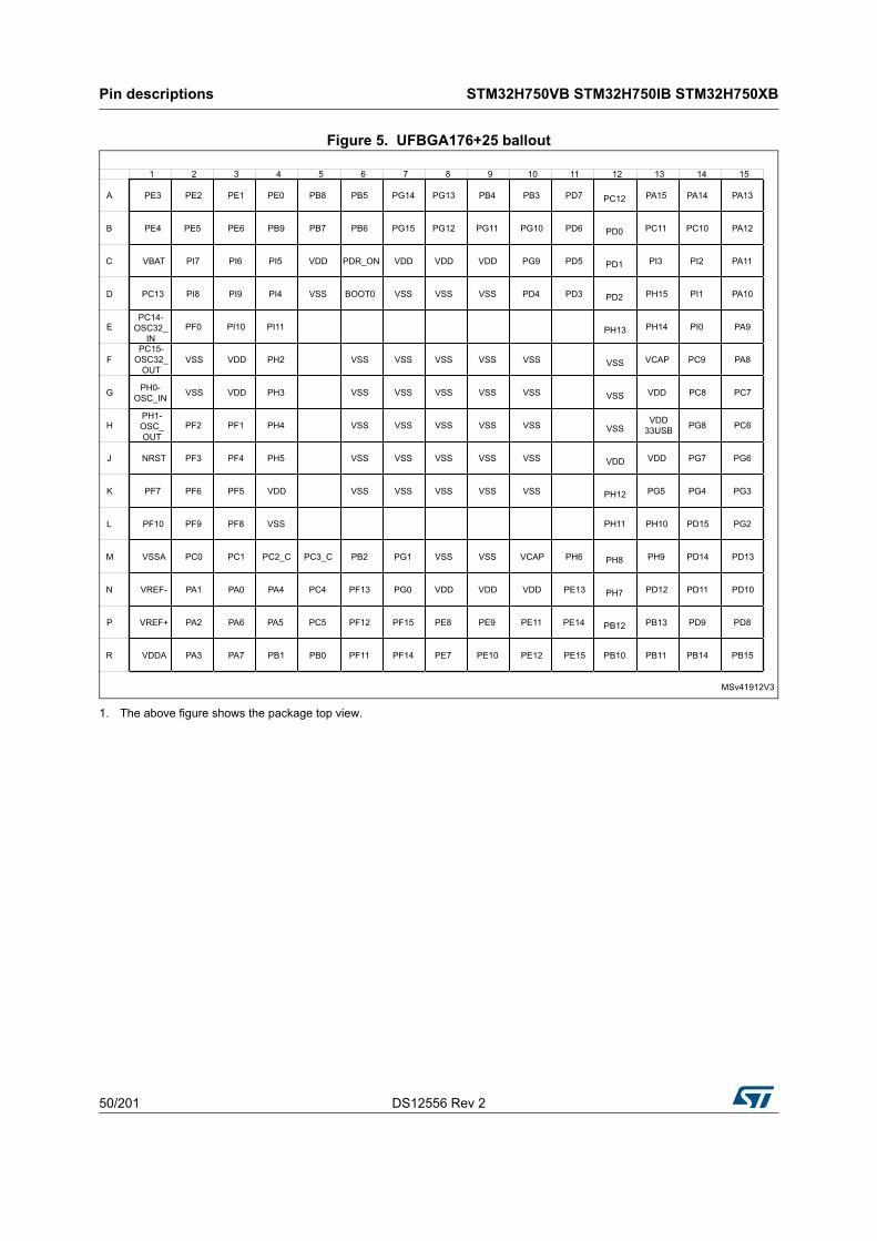
Pin descriptions STM32H750VB STM32H750IB STM32H750XB
50/201 DS12556 Rev 2
Figure 5. UFBGA176+25 ballout
1. The above figure shows the package top view.
MSv41912V3
1 2 3 4 5 6 7 8 9 10 11 12 13 14 15
A PE3 PE2 PE1 PE0 PB8 PB5 PG14 PG13 PB4 PB3 PD7 PC12 PA15 PA14 PA13
B PE4 PE5 PE6 PB9 PB7 PB6 PG15 PG12 PG11 PG10 PD6 PD0 PC11 PC10 PA12
C VBAT PI7 PI6 PI5 VDD PDR_ON VDD VDD VDD PG9 PD5 PD1 PI3 PI2 PA11
D PC13 PI8 PI9 PI4 VSS BOOT0 VSS VSS VSS PD4 PD3 PD2 PH15 PI1 PA10
EPC14-
OSC32_IN
PF0 PI10 PI11 PH13 PH14 PI0 PA9
FPC15-
OSC32_OUT
VSS VDD PH2 VSS VSS VSS VSS VSS VSS VCAP PC9 PA8
G PH0-OSC_IN VSS VDD PH3 VSS VSS VSS VSS VSS VSS VDD PC8 PC7
HPH1-OSC_OUT
PF2 PF1 PH4 VSS VSS VSS VSS VSS VSSVDD
33USB PG8 PC6
J NRST PF3 PF4 PH5 VSS VSS VSS VSS VSS VDD VDD PG7 PG6
K PF7 PF6 PF5 VDD VSS VSS VSS VSS VSS PH12 PG5 PG4 PG3
L PF10 PF9 PF8 PH11 PH10 PD15 PG2
M VSSA PC0 PC1 PC2_C PC3_C PB2 PG1 VSS VSS VCAP PH6 PH8 PH9 PD14 PD13
N VREF- PA1 PA0 PA4 PC4 PF13 PG0 VDD VDD VDD PE13 PH7 PD12 PD11 PD10
P VREF+ PA2 PA6 PA5 PC5 PF12 PF15 PE8 PE9 PE11 PE14 PB12 PB13 PD9 PD8
R VDDA PA3 PA7 PB1 PB0 PF11 PF14 PE7 PE10 PE12 PE15 PB10 PB11 PB14 PB15
VSS
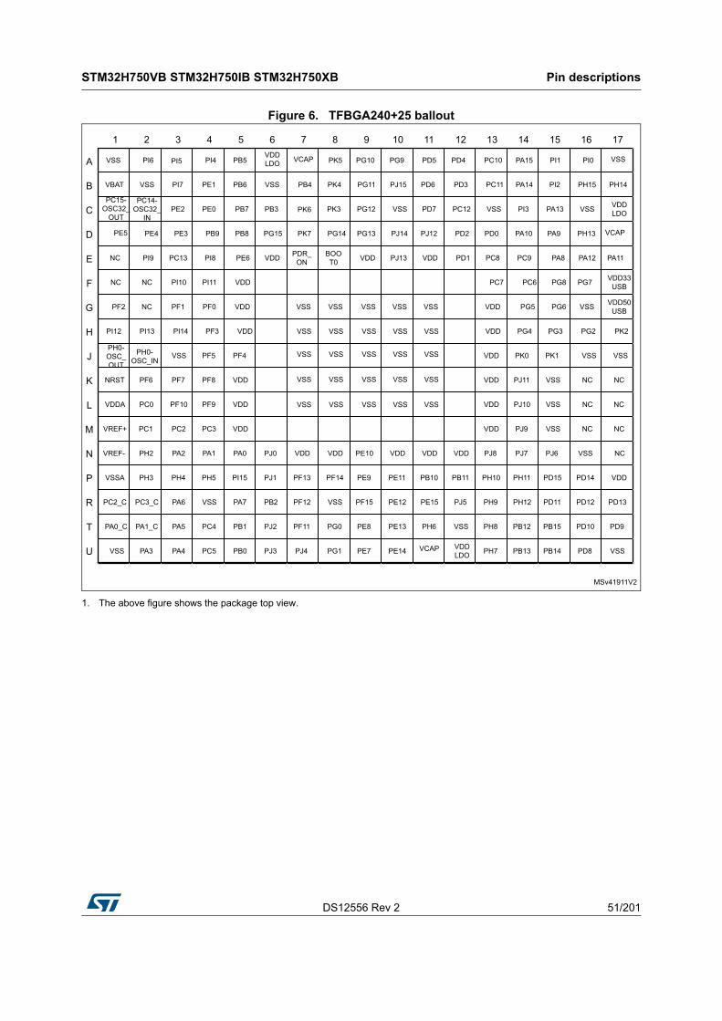
DS12556 Rev 2 51/201
STM32H750VB STM32H750IB STM32H750XB Pin descriptions
85
Figure 6. TFBGA240+25 ballout
1. The above figure shows the package top view.
MSv41911V2
VSS PI6 PI5 PI4 PB5VDDLDO VCAP PK5 PG10 PG9 PD5 PD4 PC10 PA15 PI1 PI0 VSS
VBAT VSS PI7 PE1 PB6 VSS PB4 PK4 PG11 PJ15 PD6 PD3 PC11 PA14 PI2 PH15 PH14
PC15-OSC32_
OUTPE2 PE0 PB7 PB3 PK6 PK3 PG12 VSS PD7 PC12 VSS PI3 PA13 VSS VDD
LDO
PE5 PE4 PE3 PB9 PB8 PG15 PK7 PG14 PG13 PJ14 PJ12 PD2 PD0 PA10 PA9 PH13 VCAP
NC PI9 PC13 PI8 PE6 VDD PDR_ON
BOOT0 VDD PJ13 VDD PD1 PC8 PC9 PA8 PA12 PA11
NC NC PI10 PI11 VDD PC7 PC6 PG8 PG7 VDD33USB
PF2 NC PF1 PF0 VDD VSS VSS VSS VSS VSS VDD PG5 PG6 VSS VDD50USB
PI12 PI13 PI14 PF3 VDD VDD PG4 PG3 PG2 PK2
PH0-OSC_IN
VSS PF5 PF4 VDD PK0 PK1 VSS VSS
NRST PF6 PF7 PF8 VDD VDD PJ11 VSS NC NC
VDDA PC0 PF10 PF9 VDD VDD PJ10 VSS NC NC
VREF+ PC1 PC2 PC3 VDD VDD PJ9 VSS NC NC
VREF- PH2 PA2 PA1 PA0 PJ0 VDD VDD PE10 VDD VDD VDD PJ8 PJ7 PJ6 VSS NC
VSSA PH3 PH4 PH5 PI15 PJ1 PF13 PF14 PE9 PE11 PB10 PB11 PH10 PH11 PD15 PD14 VDD
PC2_C PC3_C PA6 VSS PA7 PB2 PF12 VSS PF15 PE12 PE15 PJ5 PH9 PH12 PD11 PD12 PD13
PA0_C PA1_C PA5 PC4 PB1 PJ2 PF11 PG0 PE8 PE13 PH6 VSS PH8 PB12 PB15 PD10 PD9
VSS PA3 PA4 PC5 PB0 PJ3 PJ4 PG1 PE7 PE14 VCAP VDDLDO PH7 PB13 PB14 PD8 VSS
PC14-OSC32_
IN
VSS VSS VSS VSS VSS
VSS VSS VSS VSS VSS
VSS VSS VSS VSS VSS
VSS VSS VSS VSS VSS
PH0-OSC_OUT
A
B
C
D
E
F
G
H
J
K
L
M
N
P
R
T
U
1 2 3 4 5 6 7 8 9 10 11 12 13 14 15 16 17
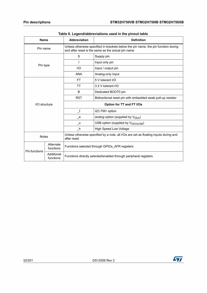
Pin descriptions STM32H750VB STM32H750IB STM32H750XB
52/201 DS12556 Rev 2
Table 6. Legend/abbreviations used in the pinout table
Name Abbreviation Definition
Pin name Unless otherwise specified in brackets below the pin name, the pin function during and after reset is the same as the actual pin name
Pin type
S Supply pin
I Input only pin
I/O Input / output pin
ANA Analog-only Input
I/O structure
FT 5 V tolerant I/O
TT 3.3 V tolerant I/O
B Dedicated BOOT0 pin
RST Bidirectional reset pin with embedded weak pull-up resistor
Option for TT and FT I/Os
_f I2C FM+ option
_a analog option (supplied by VDDA)
_u USB option (supplied by VDD33USB)
_h High Speed Low Voltage
Notes Unless otherwise specified by a note, all I/Os are set as floating inputs during and after reset.
Pin functions
Alternate functions
Functions selected through GPIOx_AFR registers
Additional functions
Functions directly selected/enabled through peripheral registers

DS12556 Rev 2 53/201
STM32H750VB STM32H750IB STM32H750XB Pin descriptions
85
Table 7. STM32H750xB pin/ball definition
Pin/ball name
Pin name (function after
reset) Pin
typ
e
I/O s
tru
ctu
re
No
tes
Alternate functionsAdditional functions
LQ
FP
100
UF
BG
A17
6+2
5
TF
BG
A2
40 +
25
1 A2 C3 PE2 I/O FT_h -
TRACECLK, SAI1_CK1, SPI4_SCK, SAI1_MCLK_A,
SAI4_MCLK_A, QUADSPI_BK1_IO2, SAI4_CK1,
ETH_MII_TXD3, FMC_A23, EVENTOUT
-
2 A1 D3 PE3 I/O FT_h -TRACED0, TIM15_BKIN, SAI1_SD_B, SAI4_SD_B, FMC_A19, EVENTOUT
-
3 B1 D2 PE4 I/O FT_h -
TRACED1, SAI1_D2, DFSDM_DATIN3, TIM15_CH1N,
SPI4_NSS, SAI1_FS_A, SAI4_FS_A, SAI4_D2, FMC_A20, DCMI_D4, LCD_B0, EVENTOUT
-
4 B2 D1 PE5 I/O FT_h -
TRACED2, SAI1_CK2, DFSDM_CKIN3, TIM15_CH1,
SPI4_MISO, SAI1_SCK_A, SAI4_SCK_A, SAI4_CK2,
FMC_A21, DCMI_D6, LCD_G0, EVENTOUT
-
5 B3 E5 PE6 I/O FT_h -
TRACED3, TIM1_BKIN2, SAI1_D1, TIM15_CH2,
SPI4_MOSI, SAI1_SD_A, SAI4_SD_A, SAI4_D1,
SAI2_MCK_B, TIM1_BKIN2_COMP12,
FMC_A22, DCMI_D7, LCD_G1, EVENTOUT
-
- H10 A1 VSS S - - - -
- - - VDD S - - - -
6 C1 B1 VBAT S - - - -
- J6 B2 VSS - - - - -
- D2 E4 PI8 I/O FT - EVENTOUTRTC_TAMP_2/
RTC_TS/WKUP3
7 D1 E3 PC13 I/O FT - EVENTOUTRTC_TAMP_1/
RTC_TS/WKUP2
- J7 B6 VSS - - - - -
8 E1 C2PC14-
OSC32_IN (OSC32_IN)(1)
I/O FT - EVENTOUT OSC32_IN

Pin descriptions STM32H750VB STM32H750IB STM32H750XB
54/201 DS12556 Rev 2
9 F1 C1PC15-
OSC32_OUT (OSC32_OUT)(1)
I/O FT - EVENTOUTOSC32_
OUT
- D3 E2 PI9 I/O FT_h -UART4_RX, FDCAN1_RX, FMC_D30, LCD_VSYNC,
EVENTOUT-
- E3 F3 PI10 I/O FT_h -FDCAN1_RXFD_MODE,
ETH_MII_RX_ER, FMC_D31, LCD_HSYNC, EVENTOUT
- E4 F4 PI11 I/O FT -LCD_G6, OTG_HS_ULPI_DIR,
EVENTOUTWKUP4
- F2 A17 VSS S - - - -
- F3 E6 VDD S - - - -
- - E1(2) NC - - - - -
- - F1(3) NC - - - - -
- - G2(4) NC - - - - -
- E2 G4 PF0 I/O FT_f - I2C2_SDA, FMC_A0, EVENTOUT -
- H3 G3 PF1 I/O FT_f - I2C2_SCL, FMC_A1, EVENTOUT -
- H2 G1 PF2 I/O FT -I2C2_SMBA, FMC_A2,
EVENTOUT-
- - H1 PI12 I/O FT -ETH_TX_ER, LCD_HSYNC,
EVENTOUT-
- - H2 PI13 I/O FT - LCD_VSYNC, EVENTOUT -
- - H3 PI14 I/O FT_h - LCD_CLK, EVENTOUT -
- J2 H4 PF3 I/O FT_ha - FMC_A3, EVENTOUT ADC3_INP5
- J3 J5 PF4 I/O FT_ha - FMC_A4, EVENTOUTADC3_INN5, ADC3_INP9
- K3 J4 PF5 I/O FT_ha - FMC_A5, EVENTOUT ADC3_INP4
10 G2 C10 VSS S - - - -
11 G3 E9 VDD S - - - -
- K2 K2 PF6 I/O FT_ha -
TIM16_CH1, SPI5_NSS, SAI1_SD_B, UART7_RX,
SAI4_SD_B, QUADSPI_BK1_IO3, EVENTOUT
ADC3_INN4, ADC3_INP8
- K1 K3 PF7 I/O FT_ha -
TIM17_CH1, SPI5_SCK, SAI1_MCLK_B, UART7_TX,
SAI4_MCLK_B, QUADSPI_BK1_IO2, EVENTOUT
ADC3_INP3
Table 7. STM32H750xB pin/ball definition (continued)
Pin/ball name
Pin name (function after
reset) Pin
typ
e
I/O
str
uct
ure
No
tes
Alternate functionsAdditional functions
LQ
FP
100
UF
BG
A17
6+25
TF
BG
A24
0 +
25
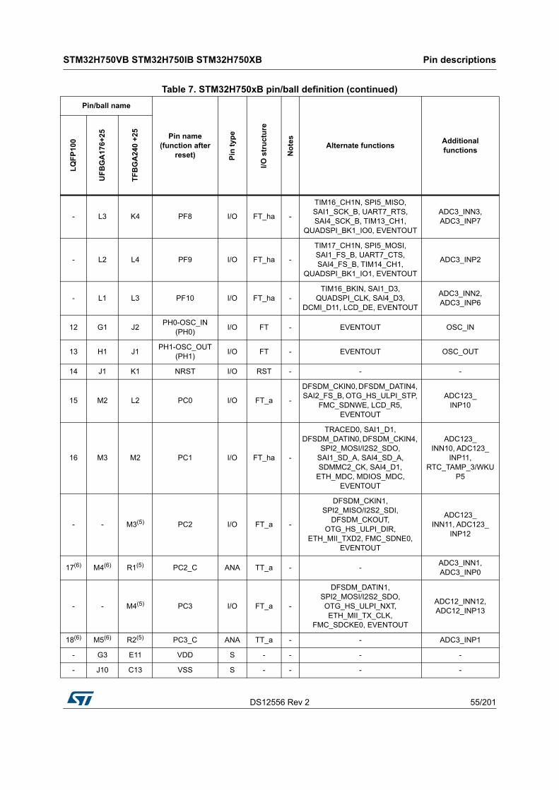
DS12556 Rev 2 55/201
STM32H750VB STM32H750IB STM32H750XB Pin descriptions
85
- L3 K4 PF8 I/O FT_ha -
TIM16_CH1N, SPI5_MISO, SAI1_SCK_B, UART7_RTS, SAI4_SCK_B, TIM13_CH1,
QUADSPI_BK1_IO0, EVENTOUT
ADC3_INN3, ADC3_INP7
- L2 L4 PF9 I/O FT_ha -
TIM17_CH1N, SPI5_MOSI, SAI1_FS_B, UART7_CTS, SAI4_FS_B, TIM14_CH1,
QUADSPI_BK1_IO1, EVENTOUT
ADC3_INP2
- L1 L3 PF10 I/O FT_ha -TIM16_BKIN, SAI1_D3,
QUADSPI_CLK, SAI4_D3, DCMI_D11, LCD_DE, EVENTOUT
ADC3_INN2, ADC3_INP6
12 G1 J2PH0-OSC_IN
(PH0)I/O FT - EVENTOUT OSC_IN
13 H1 J1PH1-OSC_OUT
(PH1)I/O FT - EVENTOUT OSC_OUT
14 J1 K1 NRST I/O RST - - -
15 M2 L2 PC0 I/O FT_a -
DFSDM_CKIN0, DFSDM_DATIN4, SAI2_FS_B, OTG_HS_ULPI_STP,
FMC_SDNWE, LCD_R5, EVENTOUT
ADC123_INP10
16 M3 M2 PC1 I/O FT_ha -
TRACED0, SAI1_D1, DFSDM_DATIN0, DFSDM_CKIN4,
SPI2_MOSI/I2S2_SDO, SAI1_SD_A, SAI4_SD_A, SDMMC2_CK, SAI4_D1,
ETH_MDC, MDIOS_MDC, EVENTOUT
ADC123_INN10, ADC123_
INP11, RTC_TAMP_3/WKU
P5
- - M3(5) PC2 I/O FT_a -
DFSDM_CKIN1, SPI2_MISO/I2S2_SDI,
DFSDM_CKOUT, OTG_HS_ULPI_DIR,
ETH_MII_TXD2, FMC_SDNE0, EVENTOUT
ADC123_INN11, ADC123_
INP12
17(6) M4(6) R1(5) PC2_C ANA TT_a - -ADC3_INN1, ADC3_INP0
- - M4(5) PC3 I/O FT_a -
DFSDM_DATIN1, SPI2_MOSI/I2S2_SDO, OTG_HS_ULPI_NXT, ETH_MII_TX_CLK,
FMC_SDCKE0, EVENTOUT
ADC12_INN12, ADC12_INP13
18(6) M5(6) R2(5) PC3_C ANA TT_a - - ADC3_INP1
- G3 E11 VDD S - - - -
- J10 C13 VSS S - - - -
Table 7. STM32H750xB pin/ball definition (continued)
Pin/ball name
Pin name (function after
reset) Pin
typ
e
I/O
str
uct
ure
No
tes
Alternate functionsAdditional functions
LQ
FP
100
UF
BG
A17
6+25
TF
BG
A24
0 +
25

Pin descriptions STM32H750VB STM32H750IB STM32H750XB
56/201 DS12556 Rev 2
19 M1 P1 VSSA S - - - -
- N1 N1 VREF- S - - - -
20 P1 M1 VREF+ S - - - -
21 R1 L1 VDDA S - - - -
22 N3 N5(5) PA0 I/O FT_a -
TIM2_CH1/TIM2_ETR, TIM5_CH1, TIM8_ETR,
TIM15_BKIN, USART2_CTS_NSS, UART4_TX,
SDMMC2_CMD, SAI2_SD_B, ETH_MII_CRS, EVENTOUT
ADC1_INP16, WKUP0
- - T1(5) PA0_C ANA TT_a - -ADC12_INN1, ADC12_INP0
23 N2 N4(5) PA1 I/O FT_ha -
TIM2_CH2, TIM5_CH2, LPTIM3_OUT, TIM15_CH1N, USART2_RTS, UART4_RX,
QUADSPI_BK1_IO3, SAI2_MCK_B,
ETH_MII_RX_CLK/ETH_RMII_REF_CLK, LCD_R2, EVENTOUT
ADC1_INN16, ADC1_INP17
- - T2(5) PA1_C ANA TT_a - - ADC12_INP1
24 P2 N3 PA2 I/O FT_a -
TIM2_CH3, TIM5_CH3, LPTIM4_OUT, TIM15_CH1, USART2_TX, SAI2_SCK_B, ETH_MDIO, MDIOS_MDIO,
LCD_R1, EVENTOUT
ADC12_INP14, WKUP1
- F4 N2 PH2 I/O FT_ha -
LPTIM1_IN2, QUADSPI_BK2_IO0,
SAI2_SCK_B, ETH_MII_CRS, FMC_SDCKE0, LCD_R0,
EVENTOUT
ADC3_INP13
- - F5 VDD S - - - -
- J8 C16 VSS S - - - -
- G4 P2 PH3 I/O FT_ha -
QUADSPI_BK2_IO1, SAI2_MCK_B, ETH_MII_COL,
FMC_SDNE0, LCD_R1, EVENTOUT
ADC3_INN13, ADC3_INP14
- H4 P3 PH4 I/O FT_fa -I2C2_SCL, LCD_G5,
OTG_HS_ULPI_NXT, LCD_G4, EVENTOUT
ADC3_INN14, ADC3_INP15
- J4 P4 PH5 I/O FT_fa -I2C2_SDA, SPI5_NSS,
FMC_SDNWE, EVENTOUTADC3_INN15, ADC3_INP16
Table 7. STM32H750xB pin/ball definition (continued)
Pin/ball name
Pin name (function after
reset) Pin
typ
e
I/O
str
uct
ure
No
tes
Alternate functionsAdditional functions
LQ
FP
100
UF
BG
A17
6+25
TF
BG
A24
0 +
25
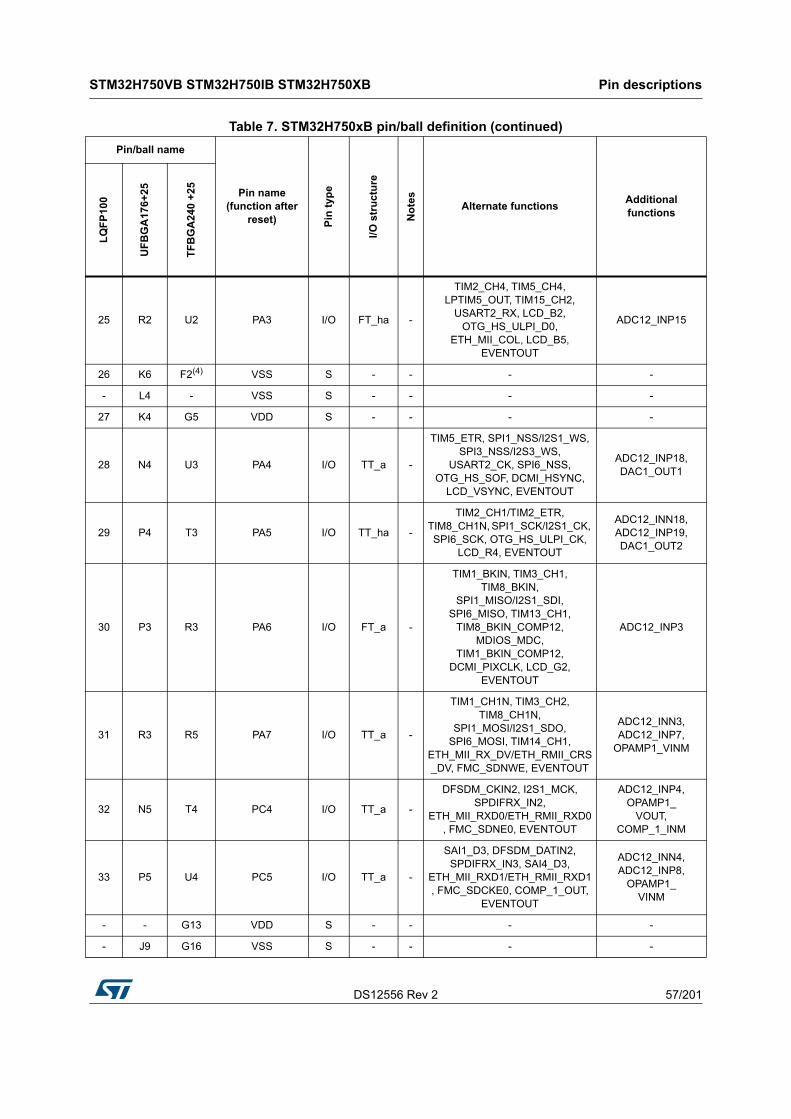
DS12556 Rev 2 57/201
STM32H750VB STM32H750IB STM32H750XB Pin descriptions
85
25 R2 U2 PA3 I/O FT_ha -
TIM2_CH4, TIM5_CH4, LPTIM5_OUT, TIM15_CH2,
USART2_RX, LCD_B2, OTG_HS_ULPI_D0,
ETH_MII_COL, LCD_B5, EVENTOUT
ADC12_INP15
26 K6 F2(4) VSS S - - - -
- L4 - VSS S - - - -
27 K4 G5 VDD S - - - -
28 N4 U3 PA4 I/O TT_a -
TIM5_ETR, SPI1_NSS/I2S1_WS, SPI3_NSS/I2S3_WS,
USART2_CK, SPI6_NSS, OTG_HS_SOF, DCMI_HSYNC,
LCD_VSYNC, EVENTOUT
ADC12_INP18, DAC1_OUT1
29 P4 T3 PA5 I/O TT_ha -
TIM2_CH1/TIM2_ETR, TIM8_CH1N, SPI1_SCK/I2S1_CK, SPI6_SCK, OTG_HS_ULPI_CK,
LCD_R4, EVENTOUT
ADC12_INN18, ADC12_INP19, DAC1_OUT2
30 P3 R3 PA6 I/O FT_a -
TIM1_BKIN, TIM3_CH1, TIM8_BKIN,
SPI1_MISO/I2S1_SDI, SPI6_MISO, TIM13_CH1,
TIM8_BKIN_COMP12, MDIOS_MDC,
TIM1_BKIN_COMP12, DCMI_PIXCLK, LCD_G2,
EVENTOUT
ADC12_INP3
31 R3 R5 PA7 I/O TT_a -
TIM1_CH1N, TIM3_CH2, TIM8_CH1N,
SPI1_MOSI/I2S1_SDO, SPI6_MOSI, TIM14_CH1,
ETH_MII_RX_DV/ETH_RMII_CRS_DV, FMC_SDNWE, EVENTOUT
ADC12_INN3, ADC12_INP7,
OPAMP1_VINM
32 N5 T4 PC4 I/O TT_a -
DFSDM_CKIN2, I2S1_MCK, SPDIFRX_IN2,
ETH_MII_RXD0/ETH_RMII_RXD0, FMC_SDNE0, EVENTOUT
ADC12_INP4, OPAMP1_
VOUT, COMP_1_INM
33 P5 U4 PC5 I/O TT_a -
SAI1_D3, DFSDM_DATIN2, SPDIFRX_IN3, SAI4_D3,
ETH_MII_RXD1/ETH_RMII_RXD1, FMC_SDCKE0, COMP_1_OUT,
EVENTOUT
ADC12_INN4, ADC12_INP8,
OPAMP1_VINM
- - G13 VDD S - - - -
- J9 G16 VSS S - - - -
Table 7. STM32H750xB pin/ball definition (continued)
Pin/ball name
Pin name (function after
reset) Pin
typ
e
I/O
str
uct
ure
No
tes
Alternate functionsAdditional functions
LQ
FP
100
UF
BG
A17
6+25
TF
BG
A24
0 +
25
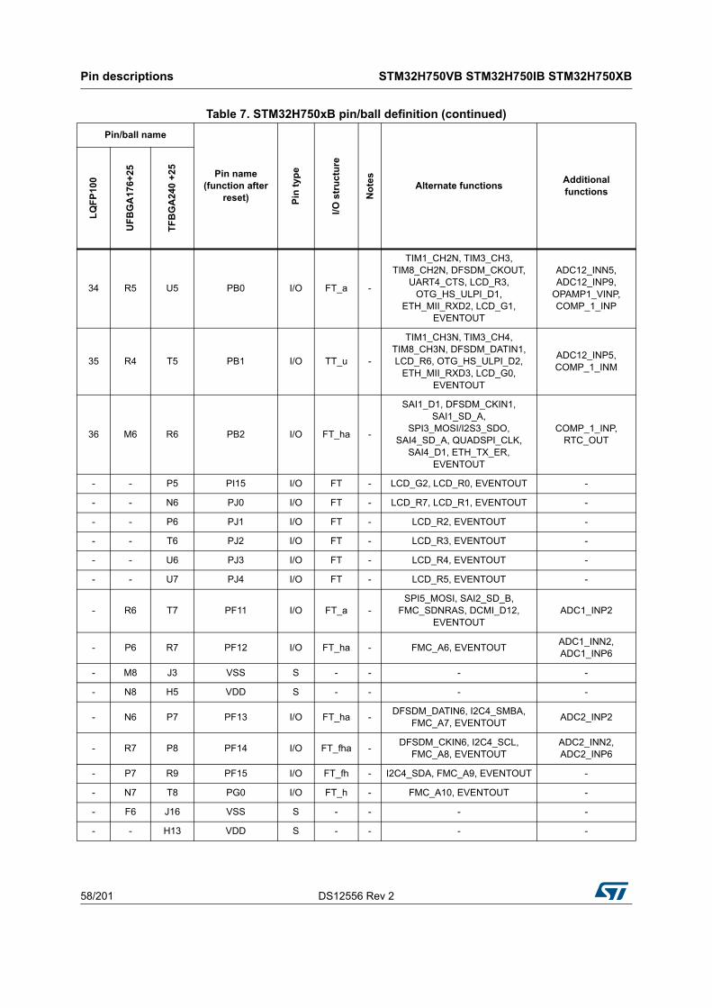
Pin descriptions STM32H750VB STM32H750IB STM32H750XB
58/201 DS12556 Rev 2
34 R5 U5 PB0 I/O FT_a -
TIM1_CH2N, TIM3_CH3, TIM8_CH2N, DFSDM_CKOUT,
UART4_CTS, LCD_R3, OTG_HS_ULPI_D1,
ETH_MII_RXD2, LCD_G1, EVENTOUT
ADC12_INN5, ADC12_INP9,
OPAMP1_VINP, COMP_1_INP
35 R4 T5 PB1 I/O TT_u -
TIM1_CH3N, TIM3_CH4, TIM8_CH3N, DFSDM_DATIN1, LCD_R6, OTG_HS_ULPI_D2,
ETH_MII_RXD3, LCD_G0, EVENTOUT
ADC12_INP5, COMP_1_INM
36 M6 R6 PB2 I/O FT_ha -
SAI1_D1, DFSDM_CKIN1, SAI1_SD_A,
SPI3_MOSI/I2S3_SDO, SAI4_SD_A, QUADSPI_CLK,
SAI4_D1, ETH_TX_ER, EVENTOUT
COMP_1_INP, RTC_OUT
- - P5 PI15 I/O FT - LCD_G2, LCD_R0, EVENTOUT -
- - N6 PJ0 I/O FT - LCD_R7, LCD_R1, EVENTOUT -
- - P6 PJ1 I/O FT - LCD_R2, EVENTOUT -
- - T6 PJ2 I/O FT - LCD_R3, EVENTOUT -
- - U6 PJ3 I/O FT - LCD_R4, EVENTOUT -
- - U7 PJ4 I/O FT - LCD_R5, EVENTOUT -
- R6 T7 PF11 I/O FT_a -SPI5_MOSI, SAI2_SD_B,
FMC_SDNRAS, DCMI_D12, EVENTOUT
ADC1_INP2
- P6 R7 PF12 I/O FT_ha - FMC_A6, EVENTOUTADC1_INN2, ADC1_INP6
- M8 J3 VSS S - - - -
- N8 H5 VDD S - - - -
- N6 P7 PF13 I/O FT_ha -DFSDM_DATIN6, I2C4_SMBA,
FMC_A7, EVENTOUTADC2_INP2
- R7 P8 PF14 I/O FT_fha -DFSDM_CKIN6, I2C4_SCL,
FMC_A8, EVENTOUTADC2_INN2, ADC2_INP6
- P7 R9 PF15 I/O FT_fh - I2C4_SDA, FMC_A9, EVENTOUT -
- N7 T8 PG0 I/O FT_h - FMC_A10, EVENTOUT -
- F6 J16 VSS S - - - -
- - H13 VDD S - - - -
Table 7. STM32H750xB pin/ball definition (continued)
Pin/ball name
Pin name (function after
reset) Pin
typ
e
I/O
str
uct
ure
No
tes
Alternate functionsAdditional functions
LQ
FP
100
UF
BG
A17
6+25
TF
BG
A24
0 +
25
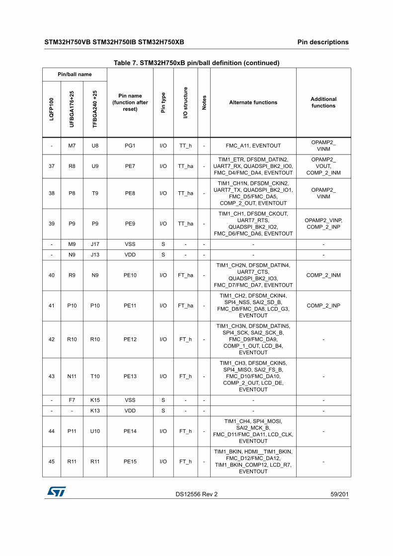
DS12556 Rev 2 59/201
STM32H750VB STM32H750IB STM32H750XB Pin descriptions
85
- M7 U8 PG1 I/O TT_h - FMC_A11, EVENTOUTOPAMP2_
VINM
37 R8 U9 PE7 I/O TT_ha -TIM1_ETR, DFSDM_DATIN2,
UART7_RX, QUADSPI_BK2_IO0, FMC_D4/FMC_DA4, EVENTOUT
OPAMP2_VOUT,
COMP_2_INM
38 P8 T9 PE8 I/O TT_ha -
TIM1_CH1N, DFSDM_CKIN2, UART7_TX, QUADSPI_BK2_IO1,
FMC_D5/FMC_DA5, COMP_2_OUT, EVENTOUT
OPAMP2_VINM
39 P9 P9 PE9 I/O TT_ha -
TIM1_CH1, DFSDM_CKOUT, UART7_RTS,
QUADSPI_BK2_IO2, FMC_D6/FMC_DA6, EVENTOUT
OPAMP2_VINP, COMP_2_INP
- M9 J17 VSS S - - - -
- N9 J13 VDD S - - - -
40 R9 N9 PE10 I/O FT_ha -
TIM1_CH2N, DFSDM_DATIN4, UART7_CTS,
QUADSPI_BK2_IO3, FMC_D7/FMC_DA7, EVENTOUT
COMP_2_INM
41 P10 P10 PE11 I/O FT_ha -
TIM1_CH2, DFSDM_CKIN4, SPI4_NSS, SAI2_SD_B,
FMC_D8/FMC_DA8, LCD_G3, EVENTOUT
COMP_2_INP
42 R10 R10 PE12 I/O FT_h -
TIM1_CH3N, DFSDM_DATIN5, SPI4_SCK, SAI2_SCK_B,
FMC_D9/FMC_DA9, COMP_1_OUT, LCD_B4,
EVENTOUT
-
43 N11 T10 PE13 I/O FT_h -
TIM1_CH3, DFSDM_CKIN5, SPI4_MISO, SAI2_FS_B, FMC_D10/FMC_DA10,
COMP_2_OUT, LCD_DE, EVENTOUT
-
- F7 K15 VSS S - - - -
- - K13 VDD S - - - -
44 P11 U10 PE14 I/O FT_h -
TIM1_CH4, SPI4_MOSI, SAI2_MCK_B,
FMC_D11/FMC_DA11, LCD_CLK, EVENTOUT
-
45 R11 R11 PE15 I/O FT_h -
TIM1_BKIN, HDMI__TIM1_BKIN, FMC_D12/FMC_DA12,
TIM1_BKIN_COMP12, LCD_R7, EVENTOUT
-
Table 7. STM32H750xB pin/ball definition (continued)
Pin/ball name
Pin name (function after
reset) Pin
typ
e
I/O
str
uct
ure
No
tes
Alternate functionsAdditional functions
LQ
FP
100
UF
BG
A17
6+25
TF
BG
A24
0 +
25

Pin descriptions STM32H750VB STM32H750IB STM32H750XB
60/201 DS12556 Rev 2
46 R12 P11 PB10 I/O FT_f -
TIM2_CH3, HRTIM_SCOUT, LPTIM2_IN1, I2C2_SCL,
SPI2_SCK/I2S2_CK, DFSDM_DATIN7, USART3_TX,
QUADSPI_BK1_NCS, OTG_HS_ULPI_D3,
ETH_MII_RX_ER, LCD_G4, EVENTOUT
-
47 R13 P12 PB11 I/O FT_f -
TIM2_CH4, HRTIM_SCIN, LPTIM2_ETR, I2C2_SDA,
DFSDM_CKIN7, USART3_RX, OTG_HS_ULPI_D4,
ETH_MII_TX_EN/ETH_RMII_TX_EN, LCD_G5, EVENTOUT
-
48 M10 U11 VCAPVCAP S - - - -
49 K7 L15 VSS S - - - -
- - U12 VDDLDO S - - - -
50 N10 L13 VDD S - - - -
- - R12 PJ5 I/O FT - LCD_R6, EVENTOUT -
- M11 T11 PH6 I/O FT -
TIM12_CH1, I2C2_SMBA, SPI5_SCK, ETH_MII_RXD2,
FMC_SDNE1, DCMI_D8, EVENTOUT
-
- N12 U13 PH7 I/O FT_fa -I2C3_SCL, SPI5_MISO,
ETH_MII_RXD3, FMC_SDCKE1, DCMI_D9, EVENTOUT
-
- M12 T13 PH8 I/O FT_fha -TIM5_ETR, I2C3_SDA, FMC_D16,
DCMI_HSYNC, LCD_R2, EVENTOUT
-
- F8 M15 VSS S - - - -
- - M13 VDD S - - - -
- M13 R13 PH9 I/O FT_h -TIM12_CH2, I2C3_SMBA,
FMC_D17, DCMI_D0, LCD_R3, EVENTOUT
-
- L13 P13 PH10 I/O FT_h -TIM5_CH1, I2C4_SMBA,
FMC_D18, DCMI_D1, LCD_R4, EVENTOUT
-
- L12 P14 PH11 I/O FT_fh -TIM5_CH2, I2C4_SCL, FMC_D19, DCMI_D2, LCD_R5, EVENTOUT
-
- K12 R14 PH12 I/O FT_fh -TIM5_CH3, I2C4_SDA, FMC_D20, DCMI_D3, LCD_R6, EVENTOUT
-
Table 7. STM32H750xB pin/ball definition (continued)
Pin/ball name
Pin name (function after
reset) Pin
typ
e
I/O
str
uct
ure
No
tes
Alternate functionsAdditional functions
LQ
FP
100
UF
BG
A17
6+25
TF
BG
A24
0 +
25

DS12556 Rev 2 61/201
STM32H750VB STM32H750IB STM32H750XB Pin descriptions
85
- H12 N16 VSS S - - - -
- J12 P17 VDD S - - - -
51 P12 T14 PB12 I/O FT_u -
TIM1_BKIN, I2C2_SMBA, SPI2_NSS/I2S2_WS,
DFSDM_DATIN1, USART3_CK, FDCAN2_RX, OTG_HS_ULPI_D5, ETH_MII_TXD0/ETH_RMII_TXD0,
OTG_HS_ID, TIM1_BKIN_COMP12,
UART5_RX, EVENTOUT
52 P13 U14 PB13 I/O FT_u -
TIM1_CH1N, LPTIM2_OUT, SPI2_SCK/I2S2_CK,
DFSDM_CKIN1, USART3_CTS_NSS,
FDCAN2_TX, OTG_HS_ULPI_D6, ETH_MII_TXD1/ETH_RMII_TXD1,
UART5_TX, EVENTOUT
OTG_HS_VBUS
53 R14 U15 PB14 I/O FT_u -
TIM1_CH2N, TIM12_CH1, TIM8_CH2N, USART1_TX,
SPI2_MISO/I2S2_SDI, DFSDM_DATIN2, USART3_RTS,
UART4_RTS, SDMMC2_D0, OTG_HS_DM, EVENTOUT
-
54 R15 T15 PB15 I/O FT_u -
RTC_REFIN, TIM1_CH3N, TIM12_CH2, TIM8_CH3N,
USART1_RX, SPI2_MOSI/I2S2_SDO,
DFSDM_CKIN2, UART4_CTS, SDMMC2_D1, OTG_HS_DP,
EVENTOUT
-
55 P15 U16 PD8 I/O FT_h -
DFSDM_CKIN3, SAI3_SCK_B, USART3_TX, SPDIFRX_IN1,
FMC_D13/FMC_DA13, EVENTOUT
-
56 P14 T17 PD9 I/O FT_h -
DFSDM_DATIN3, SAI3_SD_B, USART3_RX,
FDCAN2_RXFD_MODE, FMC_D14/FMC_DA14,
EVENTOUT
-
57 N15 T16 PD10 I/O FT_h -
DFSDM_CKOUT, SAI3_FS_B, USART3_CK,
FDCAN2_TXFD_MODE, FMC_D15/FMC_DA15, LCD_B3,
EVENTOUT
-
- - N12 VDD S - - - -
Table 7. STM32H750xB pin/ball definition (continued)
Pin/ball name
Pin name (function after
reset) Pin
typ
e
I/O
str
uct
ure
No
tes
Alternate functionsAdditional functions
LQ
FP
100
UF
BG
A17
6+25
TF
BG
A24
0 +
25

Pin descriptions STM32H750VB STM32H750IB STM32H750XB
62/201 DS12556 Rev 2
- F9 U17 VSS S - - - -
58 N14 R15 PD11 I/O FT_h -
LPTIM2_IN2, I2C4_SMBA, USART3_CTS_NSS,
QUADSPI_BK1_IO0, SAI2_SD_A, FMC_A16, EVENTOUT
-
59 N13 R16 PD12 I/O FT_fh -
LPTIM1_IN1, TIM4_CH1, LPTIM2_IN1, I2C4_SCL,
USART3_RTS, QUADSPI_BK1_IO1, SAI2_FS_A,
FMC_A17, EVENTOUT
-
60 M15 R17 PD13 I/O FT_fh -
LPTIM1_OUT, TIM4_CH2, I2C4_SDA, QUADSPI_BK1_IO3,
SAI2_SCK_A, FMC_A18, EVENTOUT
-
- K8 T12 VSS S - - - -
- J13 N11 VDD S - - - -
61 M14 P16 PD14 I/O FT_h -TIM4_CH3, SAI3_MCLK_B,
UART8_CTS, FMC_D0/FMC_DA0, EVENTOUT
-
62 L14 P15 PD15 I/O FT_h -TIM4_CH4, SAI3_MCLK_A,
UART8_RTS, FMC_D1/FMC_DA1, EVENTOUT
-
- - N15 PJ6 I/O FT - TIM8_CH2, LCD_R7, EVENTOUT -
- - N14 PJ7 I/O FT -TRGIN, TIM8_CH2N, LCD_G0,
EVENTOUT-
- - N10 VDD S - -
- F10 R8 VSS S - -
- - N13 PJ8 I/O FT -TIM1_CH3N, TIM8_CH1,
UART8_TX, LCD_G1, EVENTOUT-
- - M14 PJ9 I/O FT -TIM1_CH3, TIM8_CH1N,
UART8_RX, LCD_G2, EVENTOUT
-
- - L14 PJ10 I/O FT -TIM1_CH2N, TIM8_CH2,
SPI5_MOSI, LCD_G3, EVENTOUT
-
- - K14 PJ11 I/O FT -TIM1_CH2, TIM8_CH2N,
SPI5_MISO, LCD_G4, EVENTOUT
-
- - N8 VDD S - -
- G6 U1 VSS S - - - -
Table 7. STM32H750xB pin/ball definition (continued)
Pin/ball name
Pin name (function after
reset) Pin
typ
e
I/O
str
uct
ure
No
tes
Alternate functionsAdditional functions
LQ
FP
100
UF
BG
A17
6+25
TF
BG
A24
0 +
25
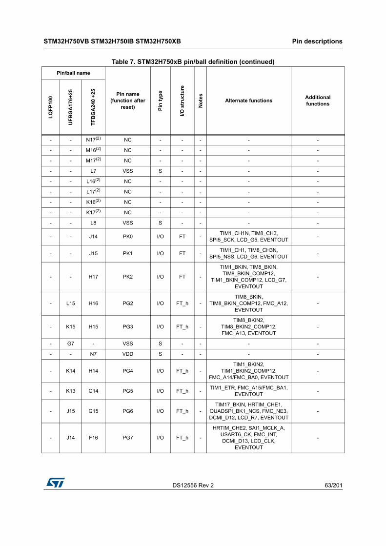
DS12556 Rev 2 63/201
STM32H750VB STM32H750IB STM32H750XB Pin descriptions
85
- - N17(2) NC - - - - -
- - M16(2) NC - - - - -
- - M17(2) NC - - - - -
- - L7 VSS S - - - -
- - L16(2) NC - - - - -
- - L17(2) NC - - - - -
- - K16(2) NC - - - - -
- - K17(2) NC - - - - -
- - L8 VSS S - - - -
- - J14 PK0 I/O FT -TIM1_CH1N, TIM8_CH3,
SPI5_SCK, LCD_G5, EVENTOUT-
- - J15 PK1 I/O FT -TIM1_CH1, TIM8_CH3N,
SPI5_NSS, LCD_G6, EVENTOUT-
- - H17 PK2 I/O FT -
TIM1_BKIN, TIM8_BKIN, TIM8_BKIN_COMP12,
TIM1_BKIN_COMP12, LCD_G7, EVENTOUT
-
- L15 H16 PG2 I/O FT_h -TIM8_BKIN,
TIM8_BKIN_COMP12, FMC_A12, EVENTOUT
-
- K15 H15 PG3 I/O FT_h -TIM8_BKIN2,
TIM8_BKIN2_COMP12, FMC_A13, EVENTOUT
-
- G7 - VSS S - - - -
- - N7 VDD S - - - -
- K14 H14 PG4 I/O FT_h -TIM1_BKIN2,
TIM1_BKIN2_COMP12, FMC_A14/FMC_BA0, EVENTOUT
-
- K13 G14 PG5 I/O FT_h -TIM1_ETR, FMC_A15/FMC_BA1,
EVENTOUT-
- J15 G15 PG6 I/O FT_h -TIM17_BKIN, HRTIM_CHE1,
QUADSPI_BK1_NCS, FMC_NE3, DCMI_D12, LCD_R7, EVENTOUT
-
- J14 F16 PG7 I/O FT_h -
HRTIM_CHE2, SAI1_MCLK_A, USART6_CK, FMC_INT, DCMI_D13, LCD_CLK,
EVENTOUT
-
Table 7. STM32H750xB pin/ball definition (continued)
Pin/ball name
Pin name (function after
reset) Pin
typ
e
I/O
str
uct
ure
No
tes
Alternate functionsAdditional functions
LQ
FP
100
UF
BG
A17
6+25
TF
BG
A24
0 +
25
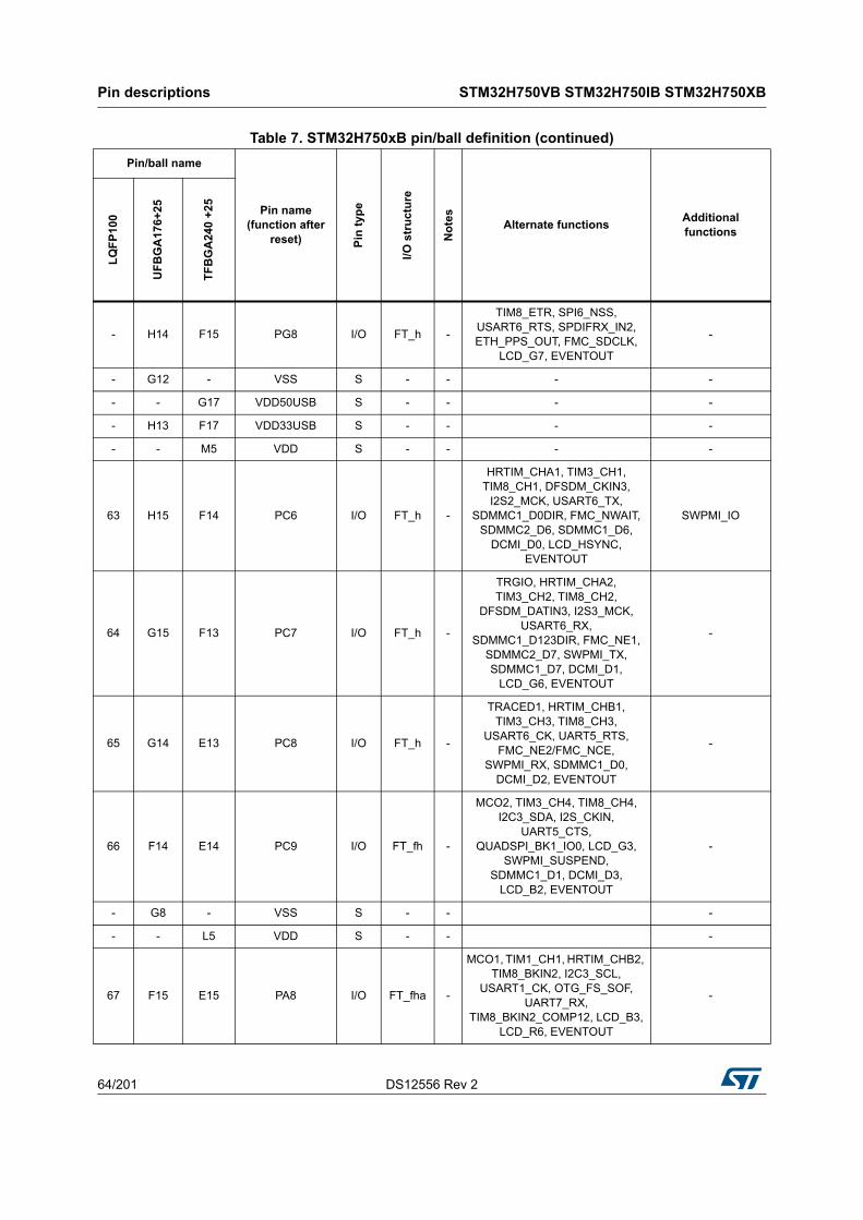
Pin descriptions STM32H750VB STM32H750IB STM32H750XB
64/201 DS12556 Rev 2
- H14 F15 PG8 I/O FT_h -
TIM8_ETR, SPI6_NSS, USART6_RTS, SPDIFRX_IN2, ETH_PPS_OUT, FMC_SDCLK,
LCD_G7, EVENTOUT
-
- G12 - VSS S - - - -
- - G17 VDD50USB S - - - -
- H13 F17 VDD33USB S - - - -
- - M5 VDD S - - - -
63 H15 F14 PC6 I/O FT_h -
HRTIM_CHA1, TIM3_CH1, TIM8_CH1, DFSDM_CKIN3,
I2S2_MCK, USART6_TX, SDMMC1_D0DIR, FMC_NWAIT,
SDMMC2_D6, SDMMC1_D6, DCMI_D0, LCD_HSYNC,
EVENTOUT
SWPMI_IO
64 G15 F13 PC7 I/O FT_h -
TRGIO, HRTIM_CHA2, TIM3_CH2, TIM8_CH2,
DFSDM_DATIN3, I2S3_MCK, USART6_RX,
SDMMC1_D123DIR, FMC_NE1, SDMMC2_D7, SWPMI_TX, SDMMC1_D7, DCMI_D1,
LCD_G6, EVENTOUT
-
65 G14 E13 PC8 I/O FT_h -
TRACED1, HRTIM_CHB1, TIM3_CH3, TIM8_CH3,
USART6_CK, UART5_RTS, FMC_NE2/FMC_NCE,
SWPMI_RX, SDMMC1_D0, DCMI_D2, EVENTOUT
-
66 F14 E14 PC9 I/O FT_fh -
MCO2, TIM3_CH4, TIM8_CH4, I2C3_SDA, I2S_CKIN,
UART5_CTS, QUADSPI_BK1_IO0, LCD_G3,
SWPMI_SUSPEND, SDMMC1_D1, DCMI_D3,
LCD_B2, EVENTOUT
-
- G8 - VSS S - - -
- - L5 VDD S - - -
67 F15 E15 PA8 I/O FT_fha -
MCO1, TIM1_CH1, HRTIM_CHB2, TIM8_BKIN2, I2C3_SCL,
USART1_CK, OTG_FS_SOF, UART7_RX,
TIM8_BKIN2_COMP12, LCD_B3, LCD_R6, EVENTOUT
-
Table 7. STM32H750xB pin/ball definition (continued)
Pin/ball name
Pin name (function after
reset) Pin
typ
e
I/O
str
uct
ure
No
tes
Alternate functionsAdditional functions
LQ
FP
100
UF
BG
A17
6+25
TF
BG
A24
0 +
25
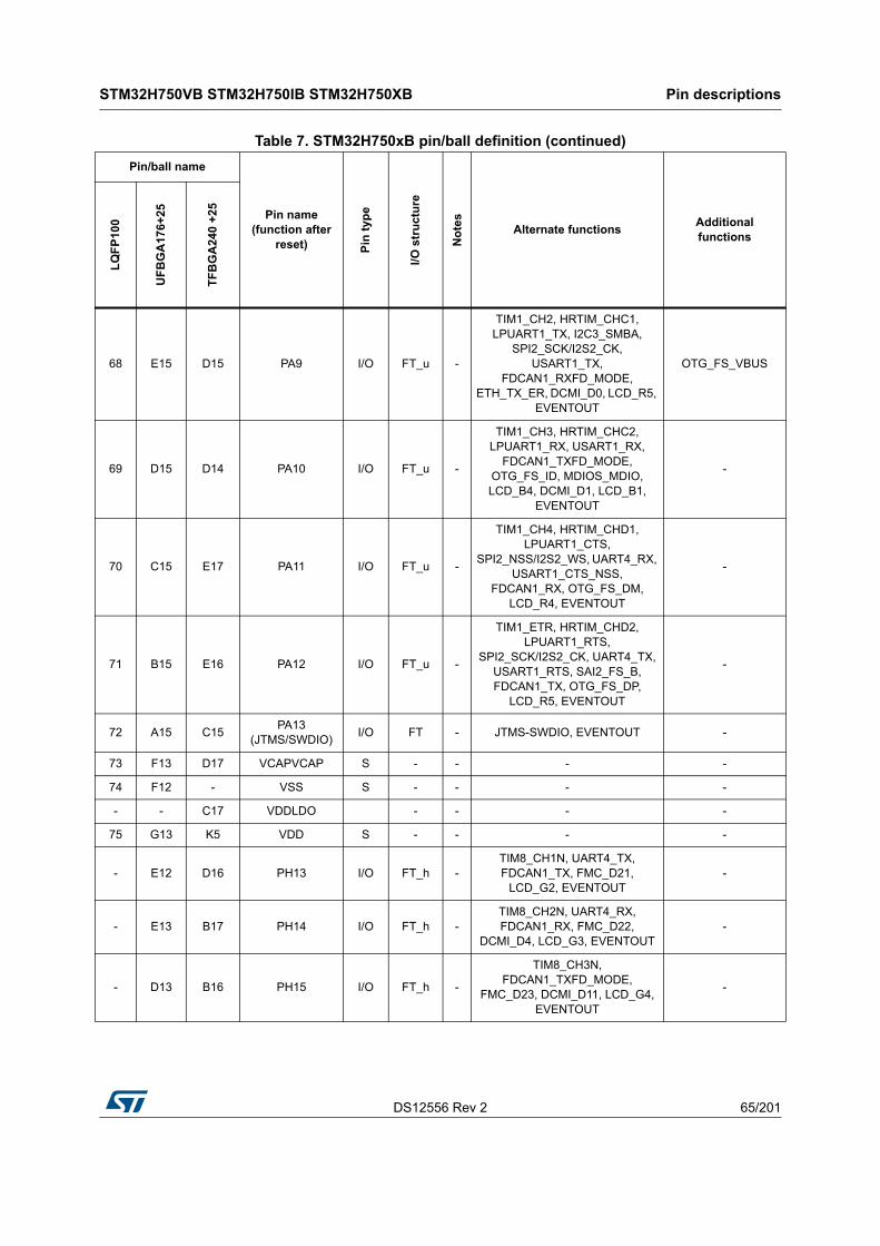
DS12556 Rev 2 65/201
STM32H750VB STM32H750IB STM32H750XB Pin descriptions
85
68 E15 D15 PA9 I/O FT_u -
TIM1_CH2, HRTIM_CHC1, LPUART1_TX, I2C3_SMBA,
SPI2_SCK/I2S2_CK, USART1_TX,
FDCAN1_RXFD_MODE, ETH_TX_ER, DCMI_D0, LCD_R5,
EVENTOUT
OTG_FS_VBUS
69 D15 D14 PA10 I/O FT_u -
TIM1_CH3, HRTIM_CHC2, LPUART1_RX, USART1_RX,
FDCAN1_TXFD_MODE, OTG_FS_ID, MDIOS_MDIO, LCD_B4, DCMI_D1, LCD_B1,
EVENTOUT
-
70 C15 E17 PA11 I/O FT_u -
TIM1_CH4, HRTIM_CHD1, LPUART1_CTS,
SPI2_NSS/I2S2_WS, UART4_RX, USART1_CTS_NSS,
FDCAN1_RX, OTG_FS_DM, LCD_R4, EVENTOUT
-
71 B15 E16 PA12 I/O FT_u -
TIM1_ETR, HRTIM_CHD2, LPUART1_RTS,
SPI2_SCK/I2S2_CK, UART4_TX, USART1_RTS, SAI2_FS_B, FDCAN1_TX, OTG_FS_DP,
LCD_R5, EVENTOUT
-
72 A15 C15PA13
(JTMS/SWDIO)I/O FT - JTMS-SWDIO, EVENTOUT -
73 F13 D17 VCAPVCAP S - - - -
74 F12 - VSS S - - - -
- - C17 VDDLDO - - - -
75 G13 K5 VDD S - - - -
- E12 D16 PH13 I/O FT_h -TIM8_CH1N, UART4_TX, FDCAN1_TX, FMC_D21,
LCD_G2, EVENTOUT-
- E13 B17 PH14 I/O FT_h -TIM8_CH2N, UART4_RX, FDCAN1_RX, FMC_D22,
DCMI_D4, LCD_G3, EVENTOUT-
- D13 B16 PH15 I/O FT_h -
TIM8_CH3N, FDCAN1_TXFD_MODE,
FMC_D23, DCMI_D11, LCD_G4, EVENTOUT
-
Table 7. STM32H750xB pin/ball definition (continued)
Pin/ball name
Pin name (function after
reset) Pin
typ
e
I/O
str
uct
ure
No
tes
Alternate functionsAdditional functions
LQ
FP
100
UF
BG
A17
6+25
TF
BG
A24
0 +
25
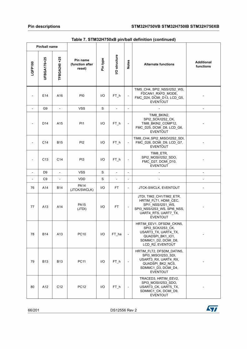
Pin descriptions STM32H750VB STM32H750IB STM32H750XB
66/201 DS12556 Rev 2
- E14 A16 PI0 I/O FT_h -
TIM5_CH4, SPI2_NSS/I2S2_WS, FDCAN1_RXFD_MODE,
FMC_D24, DCMI_D13, LCD_G5, EVENTOUT
-
- G9 - VSS S - - - -
- D14 A15 PI1 I/O FT_h -
TIM8_BKIN2, SPI2_SCK/I2S2_CK,
TIM8_BKIN2_COMP12, FMC_D25, DCMI_D8, LCD_G6,
EVENTOUT
-
- C14 B15 PI2 I/O FT_h -TIM8_CH4, SPI2_MISO/I2S2_SDI,
FMC_D26, DCMI_D9, LCD_G7, EVENTOUT
-
- C13 C14 PI3 I/O FT_h -
TIM8_ETR, SPI2_MOSI/I2S2_SDO, FMC_D27, DCMI_D10,
EVENTOUT
-
- D9 - VSS S - - - -
- C9 - VDD S - - - -
76 A14 B14PA14
(JTCK/SWCLK)I/O FT - JTCK-SWCLK, EVENTOUT -
77 A13 A14PA15(JTDI)
I/O FT -
JTDI, TIM2_CH1/TIM2_ETR, HRTIM_FLT1, HDMI_CEC,
SPI1_NSS/I2S1_WS, SPI3_NSS/I2S3_WS, SPI6_NSS,
UART4_RTS, UART7_TX, EVENTOUT
-
78 B14 A13 PC10 I/O FT_ha -
HRTIM_EEV1, DFSDM_CKIN5, SPI3_SCK/I2S3_CK,
USART3_TX, UART4_TX, QUADSPI_BK1_IO1,
SDMMC1_D2, DCMI_D8, LCD_R2, EVENTOUT
-
79 B13 B13 PC11 I/O FT_h -
HRTIM_FLT2, DFSDM_DATIN5, SPI3_MISO/I2S3_SDI,
USART3_RX, UART4_RX, QUADSPI_BK2_NCS,
SDMMC1_D3, DCMI_D4, EVENTOUT
-
80 A12 C12 PC12 I/O FT_h -
TRACED3, HRTIM_EEV2, SPI3_MOSI/I2S3_SDO,
USART3_CK, UART5_TX, SDMMC1_CK, DCMI_D9,
EVENTOUT
-
Table 7. STM32H750xB pin/ball definition (continued)
Pin/ball name
Pin name (function after
reset) Pin
typ
e
I/O
str
uct
ure
No
tes
Alternate functionsAdditional functions
LQ
FP
100
UF
BG
A17
6+25
TF
BG
A24
0 +
25
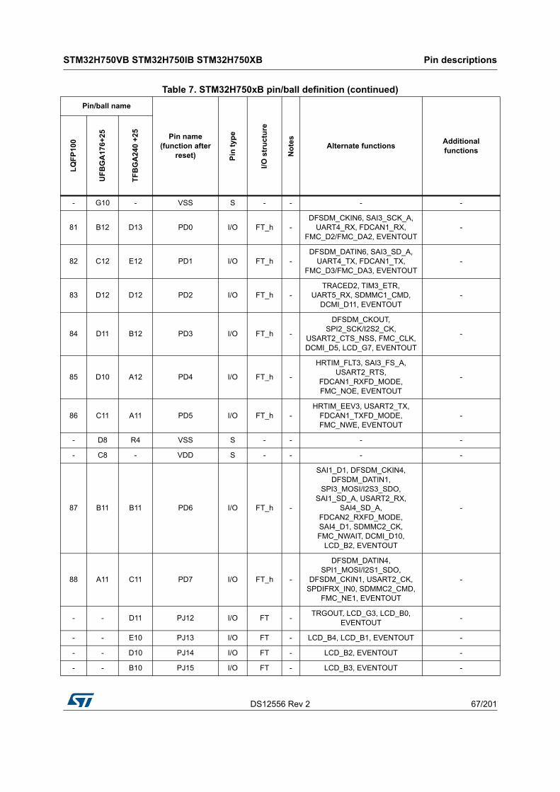
DS12556 Rev 2 67/201
STM32H750VB STM32H750IB STM32H750XB Pin descriptions
85
- G10 - VSS S - - - -
81 B12 D13 PD0 I/O FT_h -DFSDM_CKIN6, SAI3_SCK_A,
UART4_RX, FDCAN1_RX, FMC_D2/FMC_DA2, EVENTOUT
-
82 C12 E12 PD1 I/O FT_h -DFSDM_DATIN6, SAI3_SD_A,
UART4_TX, FDCAN1_TX, FMC_D3/FMC_DA3, EVENTOUT
-
83 D12 D12 PD2 I/O FT_h -TRACED2, TIM3_ETR,
UART5_RX, SDMMC1_CMD, DCMI_D11, EVENTOUT
-
84 D11 B12 PD3 I/O FT_h -
DFSDM_CKOUT, SPI2_SCK/I2S2_CK,
USART2_CTS_NSS, FMC_CLK, DCMI_D5, LCD_G7, EVENTOUT
-
85 D10 A12 PD4 I/O FT_h -
HRTIM_FLT3, SAI3_FS_A, USART2_RTS,
FDCAN1_RXFD_MODE, FMC_NOE, EVENTOUT
-
86 C11 A11 PD5 I/O FT_h -HRTIM_EEV3, USART2_TX,
FDCAN1_TXFD_MODE, FMC_NWE, EVENTOUT
-
- D8 R4 VSS S - - - -
- C8 - VDD S - - - -
87 B11 B11 PD6 I/O FT_h -
SAI1_D1, DFSDM_CKIN4, DFSDM_DATIN1,
SPI3_MOSI/I2S3_SDO, SAI1_SD_A, USART2_RX,
SAI4_SD_A, FDCAN2_RXFD_MODE, SAI4_D1, SDMMC2_CK, FMC_NWAIT, DCMI_D10,
LCD_B2, EVENTOUT
-
88 A11 C11 PD7 I/O FT_h -
DFSDM_DATIN4, SPI1_MOSI/I2S1_SDO,
DFSDM_CKIN1, USART2_CK, SPDIFRX_IN0, SDMMC2_CMD,
FMC_NE1, EVENTOUT
-
- - D11 PJ12 I/O FT -TRGOUT, LCD_G3, LCD_B0,
EVENTOUT-
- - E10 PJ13 I/O FT - LCD_B4, LCD_B1, EVENTOUT -
- - D10 PJ14 I/O FT - LCD_B2, EVENTOUT -
- - B10 PJ15 I/O FT - LCD_B3, EVENTOUT -
Table 7. STM32H750xB pin/ball definition (continued)
Pin/ball name
Pin name (function after
reset) Pin
typ
e
I/O
str
uct
ure
No
tes
Alternate functionsAdditional functions
LQ
FP
100
UF
BG
A17
6+25
TF
BG
A24
0 +
25

Pin descriptions STM32H750VB STM32H750IB STM32H750XB
68/201 DS12556 Rev 2
- H6 - VSS S - - - -
- - - VDD S - - - -
- C10 A10 PG9 I/O FT_h -
SPI1_MISO/I2S1_SDI, USART6_RX, SPDIFRX_IN3,
QUADSPI_BK2_IO2, SAI2_FS_B, FMC_NE2/FMC_NCE,
DCMI_VSYNC, EVENTOUT
-
- B10 A9 PG10 I/O FT_h -
HRTIM_FLT5, SPI1_NSS/I2S1_WS, LCD_G3,
SAI2_SD_B, FMC_NE3, DCMI_D2, LCD_B2, EVENTOUT
-
- B9 B9 PG11 I/O FT_h -
HRTIM_EEV4, SPI1_SCK/I2S1_CK,
SPDIFRX_IN0, SDMMC2_D2, ETH_MII_TX_EN/ETH_RMII_TX_
EN, DCMI_D3, LCD_B3, EVENTOUT
-
- B8 C9 PG12 I/O FT_h -
LPTIM1_IN1, HRTIM_EEV5, SPI6_MISO, USART6_RTS,
SPDIFRX_IN1, LCD_B4, ETH_MII_TXD1/ETH_RMII_TXD1, FMC_NE4, LCD_B1, EVENTOUT
-
- A8 D9 PG13 I/O FT_h -
TRACED0, LPTIM1_OUT, HRTIM_EEV10, SPI6_SCK,
USART6_CTS_NSS, ETH_MII_TXD0/ETH_RMII_TXD0, FMC_A24, LCD_R0, EVENTOUT
-
- A7 D8 PG14 I/O FT_h -
TRACED1, LPTIM1_ETR, SPI6_MOSI, USART6_TX,
QUADSPI_BK2_IO3, ETH_MII_TXD1/ETH_RMII_TXD1, FMC_A25, LCD_B0, EVENTOUT
-
- D7 - VSS S - - - -
- C7 - VDD S - - - -
- - C8 PK3 I/O FT - LCD_B4, EVENTOUT -
- - B8 PK4 I/O FT - LCD_B5, EVENTOUT -
- - A8 PK5 I/O FT - LCD_B6, EVENTOUT -
- - C7 PK6 I/O FT - LCD_B7, EVENTOUT -
- - D7 PK7 I/O FT - LCD_DE, EVENTOUT -
- H7 - VSS S - - - -
Table 7. STM32H750xB pin/ball definition (continued)
Pin/ball name
Pin name (function after
reset) Pin
typ
e
I/O
str
uct
ure
No
tes
Alternate functionsAdditional functions
LQ
FP
100
UF
BG
A17
6+25
TF
BG
A24
0 +
25
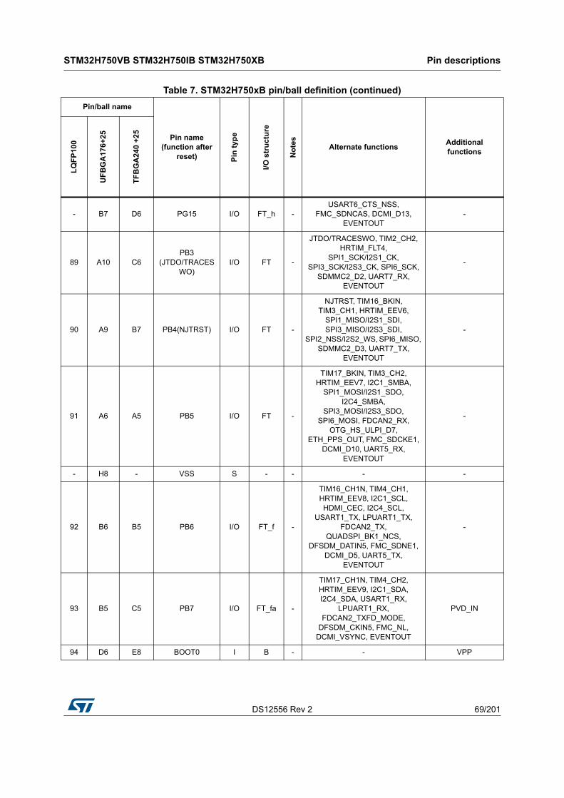
DS12556 Rev 2 69/201
STM32H750VB STM32H750IB STM32H750XB Pin descriptions
85
- B7 D6 PG15 I/O FT_h -USART6_CTS_NSS,
FMC_SDNCAS, DCMI_D13, EVENTOUT
-
89 A10 C6PB3
(JTDO/TRACESWO)
I/O FT -
JTDO/TRACESWO, TIM2_CH2, HRTIM_FLT4,
SPI1_SCK/I2S1_CK, SPI3_SCK/I2S3_CK, SPI6_SCK,
SDMMC2_D2, UART7_RX, EVENTOUT
-
90 A9 B7 PB4(NJTRST) I/O FT -
NJTRST, TIM16_BKIN, TIM3_CH1, HRTIM_EEV6,
SPI1_MISO/I2S1_SDI, SPI3_MISO/I2S3_SDI,
SPI2_NSS/I2S2_WS, SPI6_MISO, SDMMC2_D3, UART7_TX,
EVENTOUT
-
91 A6 A5 PB5 I/O FT -
TIM17_BKIN, TIM3_CH2, HRTIM_EEV7, I2C1_SMBA,
SPI1_MOSI/I2S1_SDO, I2C4_SMBA,
SPI3_MOSI/I2S3_SDO, SPI6_MOSI, FDCAN2_RX,
OTG_HS_ULPI_D7, ETH_PPS_OUT, FMC_SDCKE1,
DCMI_D10, UART5_RX, EVENTOUT
-
- H8 - VSS S - - - -
92 B6 B5 PB6 I/O FT_f -
TIM16_CH1N, TIM4_CH1, HRTIM_EEV8, I2C1_SCL, HDMI_CEC, I2C4_SCL,
USART1_TX, LPUART1_TX, FDCAN2_TX,
QUADSPI_BK1_NCS, DFSDM_DATIN5, FMC_SDNE1,
DCMI_D5, UART5_TX, EVENTOUT
-
93 B5 C5 PB7 I/O FT_fa -
TIM17_CH1N, TIM4_CH2, HRTIM_EEV9, I2C1_SDA, I2C4_SDA, USART1_RX,
LPUART1_RX, FDCAN2_TXFD_MODE,
DFSDM_CKIN5, FMC_NL, DCMI_VSYNC, EVENTOUT
PVD_IN
94 D6 E8 BOOT0 I B - - VPP
Table 7. STM32H750xB pin/ball definition (continued)
Pin/ball name
Pin name (function after
reset) Pin
typ
e
I/O
str
uct
ure
No
tes
Alternate functionsAdditional functions
LQ
FP
100
UF
BG
A17
6+25
TF
BG
A24
0 +
25
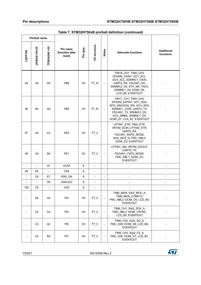
Pin descriptions STM32H750VB STM32H750IB STM32H750XB
70/201 DS12556 Rev 2
95 A5 D5 PB8 I/O FT_fh -
TIM16_CH1, TIM4_CH3, DFSDM_CKIN7, I2C1_SCL, I2C4_SCL, SDMMC1_CKIN, UART4_RX, FDCAN1_RX,
SDMMC2_D4, ETH_MII_TXD3, SDMMC1_D4, DCMI_D6,
LCD_B6, EVENTOUT
-
96 B4 D4 PB9 I/O FT_fh -
TIM17_CH1, TIM4_CH4, DFSDM_DATIN7, I2C1_SDA,
SPI2_NSS/I2S2_WS, I2C4_SDA, SDMMC1_CDIR, UART4_TX, FDCAN1_TX, SDMMC2_D5, I2C4_SMBA, SDMMC1_D5,
DCMI_D7, LCD_B7, EVENTOUT
-
97 A4 C4 PE0 I/O FT_h -
LPTIM1_ETR, TIM4_ETR, HRTIM_SCIN, LPTIM2_ETR,
UART8_RX, FDCAN1_RXFD_MODE,
SAI2_MCK_A, FMC_NBL0, DCMI_D2, EVENTOUT
-
98 A3 B4 PE1 I/O FT_h -
LPTIM1_IN2, HRTIM_SCOUT, UART8_TX,
FDCAN1_TXFD_MODE, FMC_NBL1, DCMI_D3,
EVENTOUT
-
- - A7 VCAP S - - - -
99 D5 - VSS S - - - -
- C6 E7 PDR_ON S - - - -
- - A6 VDDLDO S - - - -
100 C5 - VDD S - - - -
- D4 A4 PI4 I/O FT_h -
TIM8_BKIN, SAI2_MCK_A, TIM8_BKIN_COMP12,
FMC_NBL2, DCMI_D5, LCD_B4, EVENTOUT
-
- C4 A3 PI5 I/O FT_h -TIM8_CH1, SAI2_SCK_A,
FMC_NBL3, DCMI_VSYNC, LCD_B5, EVENTOUT
-
- C3 A2 PI6 I/O FT_h -TIM8_CH2, SAI2_SD_A,
FMC_D28, DCMI_D6, LCD_B6, EVENTOUT
-
- C2 B3 PI7 I/O FT_h -TIM8_CH3, SAI2_FS_A,
FMC_D29, DCMI_D7, LCD_B7, EVENTOUT
-
Table 7. STM32H750xB pin/ball definition (continued)
Pin/ball name
Pin name (function after
reset) Pin
typ
e
I/O
str
uct
ure
No
tes
Alternate functionsAdditional functions
LQ
FP
100
UF
BG
A17
6+25
TF
BG
A24
0 +
25
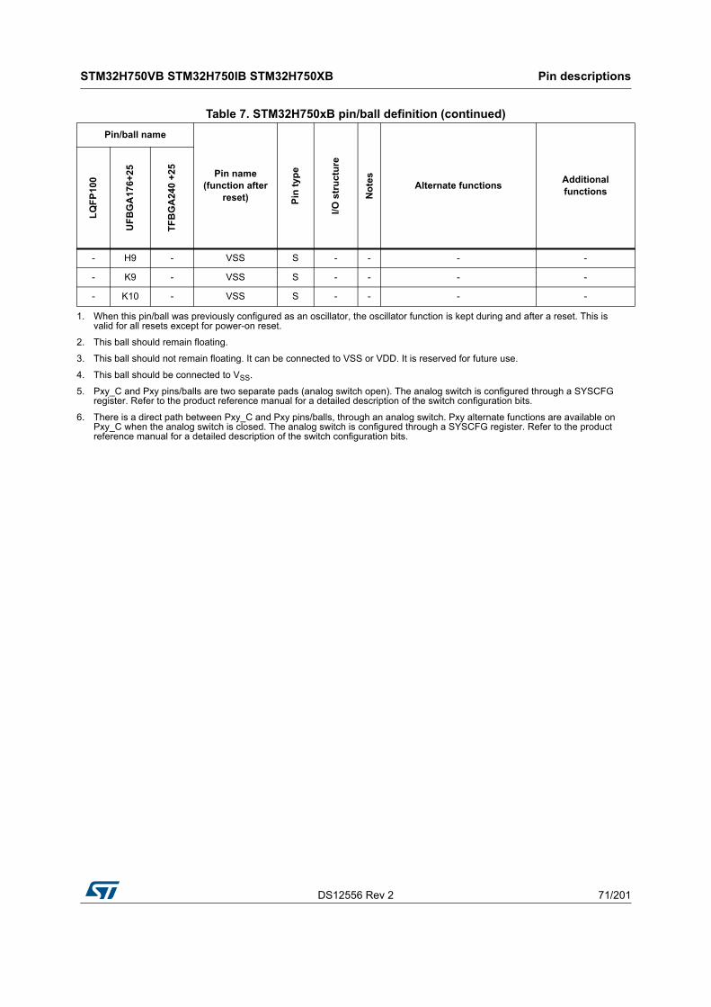
DS12556 Rev 2 71/201
STM32H750VB STM32H750IB STM32H750XB Pin descriptions
85
- H9 - VSS S - - - -
- K9 - VSS S - - - -
- K10 - VSS S - - - -
1. When this pin/ball was previously configured as an oscillator, the oscillator function is kept during and after a reset. This is valid for all resets except for power-on reset.
2. This ball should remain floating.
3. This ball should not remain floating. It can be connected to VSS or VDD. It is reserved for future use.
4. This ball should be connected to VSS.
5. Pxy_C and Pxy pins/balls are two separate pads (analog switch open). The analog switch is configured through a SYSCFG register. Refer to the product reference manual for a detailed description of the switch configuration bits.
6. There is a direct path between Pxy_C and Pxy pins/balls, through an analog switch. Pxy alternate functions are available on Pxy_C when the analog switch is closed. The analog switch is configured through a SYSCFG register. Refer to the product reference manual for a detailed description of the switch configuration bits.
Table 7. STM32H750xB pin/ball definition (continued)
Pin/ball name
Pin name (function after
reset) Pin
typ
e
I/O
str
uct
ure
No
tes
Alternate functionsAdditional functions
LQ
FP
100
UF
BG
A17
6+25
TF
BG
A24
0 +
25

Pin
des
criptio
ns
ST
M3
2H
750
VB
ST
M3
2H75
0IB S
TM
32H
75
0XB
72/2
01D
S1
2556 R
ev 2
Table 8. Port A alternate functions
Port
AF0 AF1 AF2 AF3 AF4 AF5 AF6 AF7 AF8 AF9 AF10 AF11 AF12 AF13 AF14 AF15
SYSTIM1/2/16/17/LPTIM1/HRTIM1
SAI1/TIM3/4/5/12/
HRTIM1
LPUART/TIM8/
LPTIM2/3/4/5/HRTIM1/
DFSDM
I2C1/2/3/4/USART1/TIM15/
LPTIM2/DFSDM/CEC
SPI1/2/3/4/5/6/CEC
SPI2/3/SAI1/3/I2C4/UART4/DFSDM
SPI2/3/6/USART1/2/3/6/UART7/SDMMC1
SPI6/SAI2/4/UART4/5/8/LPUART/SDMMC1/S
PDIFRX
SAI4/FDCAN1/2/TIM13/14/QUADSPI/F
MC/SDMMC2/
LCD/SPDIFRX
SAI2/4/TIM8/
QUADSPI/SDMMC2/OTG1_HS/OTG2_FS/
LCD
I2C4/UART7/
SWPMI1/TIM1/8/DFSDM/
SDMMC2/MDIOS/
ETH
TIM1/8/FMC/SDMMC1/
MDIOS/OTG1_FS/
LCD
TIM1/DCMI/LCD/COMP
UART5/LCD
SYS
Por
t A
PA0 -TIM2_CH1/TIM2_ETR
TIM5_CH1 TIM8_ETR TIM15_BKIN - -USART2_CTS_NSS
UART4_TXSDMMC2_
CMDSAI2_SD_B
ETH_MII_CRS
- - -EVENT-
OUT
PA1 - TIM2_CH2 TIM5_CH2LPTIM3_
OUTTIM15_CH1N
- -USART2_
RTSUART4_RX
QUADSPI_BK1_IO3
SAI2_MCK_B
ETH_MII_RX_CLK/
ETH_RMII_REF_CLK
- - LCD_R2EVENT-
OUT
PA2 - TIM2_CH3 TIM5_CH3LPTIM4_
OUTTIM15_CH1 - -
USART2_TX
SAI2_SCK_B
- - ETH_MDIOMDIOS_
MDIO- LCD_R1
EVENT-OUT
PA3 - TIM2_CH4 TIM5_CH4LPTIM5_
OUTTIM15_CH2 - -
USART2_RX
- LCD_B2OTG_HS_ULPI_D0
ETH_MII_COL
- - LCD_B5EVENT-
OUT
PA4 - - TIM5_ETR - -SPI1_NSS/I2S1_WS
SPI3_NSS/I2S3_WS
USART2_CK
SPI6_NSS - - -OTG_HS_
SOFDCMI_HSYNC
LCD_VSYNC
EVENT-OUT
PA5 -TIM2_CH1/TIM2_ETR
-TIM8_CH1N
-SPI1_SCK/I2S1_CK
- - SPI6_SCK -OTG_HS_ULPI_CK
- - - LCD_R4EVENT-
OUT
PA6 - TIM1_BKIN TIM3_CH1 TIM8_BKIN -SPI1_MISO/I2S1_SDI
- - SPI6_MISOTIM13_CH
1TIM8_BKIN_COMP12
MDIOS_MDC
TIM1_BKIN_COMP12
DCMI_PIXCLK
LCD_G2EVENT-
OUT
PA7 - TIM1_CH1N TIM3_CH2TIM8_CH1
N-
SPI1_MOSI/I2S1_SDO
- - SPI6_MOSITIM14_CH
1-
ETH_MII_RX_DV/
ETH_RMII_CRS_DV
FMC_SDNWE
- -EVENT-
OUT
PA8 MCO1 TIM1_CH1HRTIM_CH
B2TIM8_BKIN
2I2C3_SCL - -
USART1_CK
- -OTG_FS_
SOFUART7_RX
TIM8_BKIN2_COMP12
LCD_B3 LCD_R6EVENT-
OUT
PA9 - TIM1_CH2HRTIM_CH
C1LPUART1_
TXI2C3_SMBA
SPI2_SCK/I2S2_CK
-USART1_
TX-
FDCAN1_RXFD_MODE
-ETH_TX_
ER- DCMI_D0 LCD_R5
EVENT-OUT
PA10 - TIM1_CH3HRTIM_CH
C2LPUART1_
RX- - -
USART1_RX
-FDCAN1_
TXFD_MODE
OTG_FS_IDMDIOS_
MDIOLCD_B4 DCMI_D1 LCD_B1
EVENT-OUT
PA11 - TIM1_CH4HRTIM_CH
D1LPUART1_
CTS-
SPI2_NSS/I2S2_WS
UART4_RXUSART1_CTS_NSS
-FDCAN1_
RXOTG_FS_
DM- - - LCD_R4
EVENT-OUT
PA12 - TIM1_ETRHRTIM_CH
D2LPUART1_
RTS-
SPI2_SCK/I2S2_CK
UART4_TXUSART1_
RTSSAI2_FS_B
FDCAN1_TX
OTG_FS_DP
- - - LCD_R5EVENT-
OUT
PA13JTMS-SWDIO
- - - - - - - - - - - - - -EVENT-
OUT
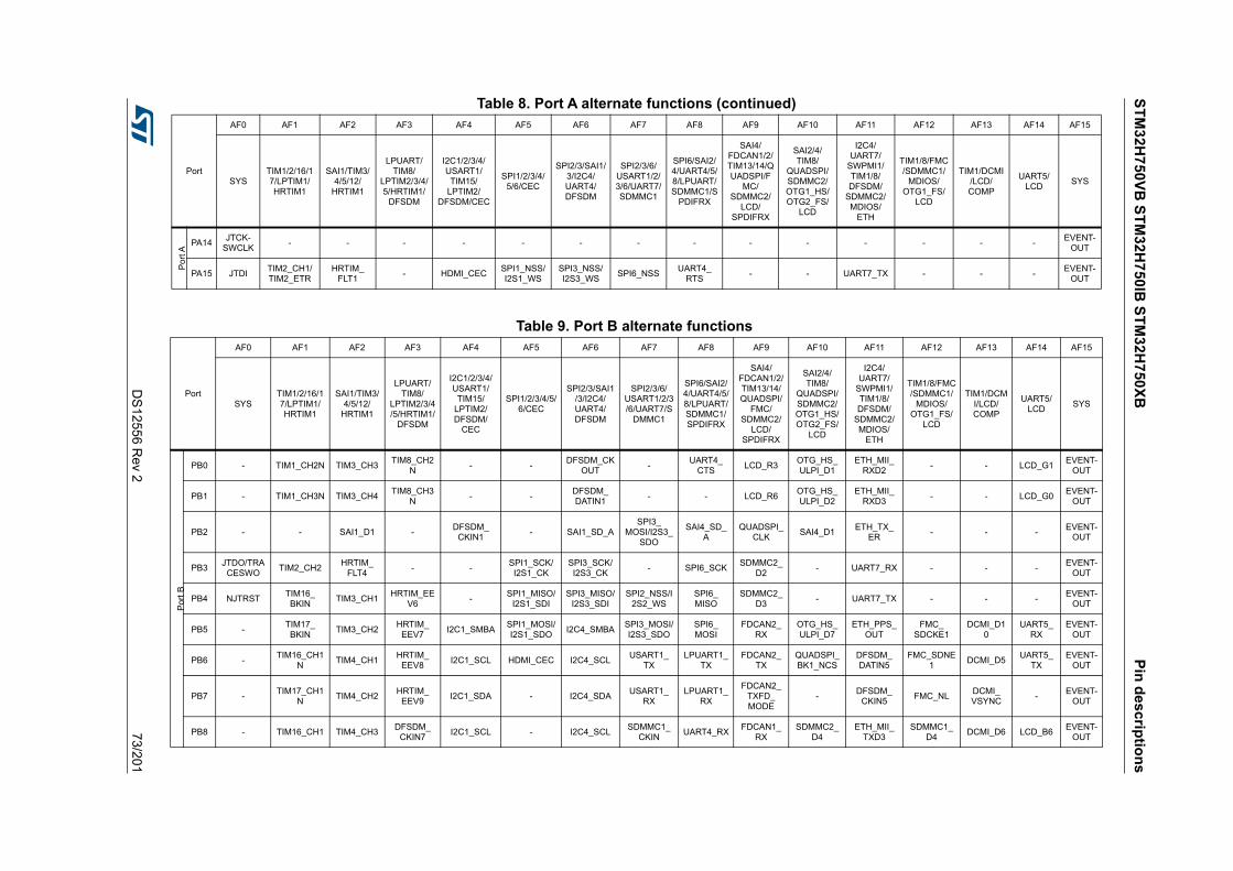
ST
M3
2H7
50V
B S
TM
32H
750
IB S
TM
32H
750
XB
Pin
de
scrip
tion
s
DS
1255
6 Rev 2
73/201
Por
t A
PA14JTCK-
SWCLK- - - - - - - - - - - - - -
EVENT-OUT
PA15 JTDITIM2_CH1/TIM2_ETR
HRTIM_FLT1
- HDMI_CECSPI1_NSS/I2S1_WS
SPI3_NSS/I2S3_WS
SPI6_NSSUART4_
RTS- - UART7_TX - - -
EVENT-OUT
Table 8. Port A alternate functions (continued)
Port
AF0 AF1 AF2 AF3 AF4 AF5 AF6 AF7 AF8 AF9 AF10 AF11 AF12 AF13 AF14 AF15
SYSTIM1/2/16/17/LPTIM1/HRTIM1
SAI1/TIM3/4/5/12/
HRTIM1
LPUART/TIM8/
LPTIM2/3/4/5/HRTIM1/
DFSDM
I2C1/2/3/4/USART1/TIM15/
LPTIM2/DFSDM/CEC
SPI1/2/3/4/5/6/CEC
SPI2/3/SAI1/3/I2C4/UART4/DFSDM
SPI2/3/6/USART1/2/3/6/UART7/SDMMC1
SPI6/SAI2/4/UART4/5/8/LPUART/SDMMC1/S
PDIFRX
SAI4/FDCAN1/2/TIM13/14/QUADSPI/F
MC/SDMMC2/
LCD/SPDIFRX
SAI2/4/TIM8/
QUADSPI/SDMMC2/OTG1_HS/OTG2_FS/
LCD
I2C4/UART7/
SWPMI1/TIM1/8/DFSDM/
SDMMC2/MDIOS/
ETH
TIM1/8/FMC/SDMMC1/
MDIOS/OTG1_FS/
LCD
TIM1/DCMI/LCD/COMP
UART5/LCD
SYS
Table 9. Port B alternate functions
Port
AF0 AF1 AF2 AF3 AF4 AF5 AF6 AF7 AF8 AF9 AF10 AF11 AF12 AF13 AF14 AF15
SYSTIM1/2/16/17/LPTIM1/HRTIM1
SAI1/TIM3/4/5/12/
HRTIM1
LPUART/TIM8/
LPTIM2/3/4/5/HRTIM1/
DFSDM
I2C1/2/3/4/USART1/TIM15/
LPTIM2/DFSDM/
CEC
SPI1/2/3/4/5/6/CEC
SPI2/3/SAI1/3/I2C4/UART4/DFSDM
SPI2/3/6/USART1/2/3/6/UART7/S
DMMC1
SPI6/SAI2/4/UART4/5/8/LPUART/SDMMC1/SPDIFRX
SAI4/FDCAN1/2/TIM13/14/QUADSPI/
FMC/SDMMC2/
LCD/SPDIFRX
SAI2/4/TIM8/
QUADSPI/SDMMC2/OTG1_HS/OTG2_FS/
LCD
I2C4/UART7/
SWPMI1/TIM1/8/DFSDM/
SDMMC2/MDIOS/
ETH
TIM1/8/FMC/SDMMC1/
MDIOS/OTG1_FS/
LCD
TIM1/DCMI/LCD/COMP
UART5/LCD
SYS
Por
t B
PB0 - TIM1_CH2N TIM3_CH3TIM8_CH2
N- -
DFSDM_CKOUT
-UART4_
CTSLCD_R3
OTG_HS_ULPI_D1
ETH_MII_RXD2
- - LCD_G1EVENT-
OUT
PB1 - TIM1_CH3N TIM3_CH4TIM8_CH3
N- -
DFSDM_DATIN1
- - LCD_R6OTG_HS_ULPI_D2
ETH_MII_RXD3
- - LCD_G0EVENT-
OUT
PB2 - - SAI1_D1 -DFSDM_
CKIN1- SAI1_SD_A
SPI3_MOSI/I2S3_
SDO
SAI4_SD_A
QUADSPI_CLK
SAI4_D1ETH_TX_
ER- - -
EVENT-OUT
PB3JTDO/TRA
CESWOTIM2_CH2
HRTIM_FLT4
- -SPI1_SCK/I2S1_CK
SPI3_SCK/I2S3_CK
- SPI6_SCKSDMMC2_
D2- UART7_RX - - -
EVENT-OUT
PB4 NJTRSTTIM16_BKIN
TIM3_CH1HRTIM_EE
V6-
SPI1_MISO/I2S1_SDI
SPI3_MISO/I2S3_SDI
SPI2_NSS/I2S2_WS
SPI6_MISO
SDMMC2_D3
- UART7_TX - - -EVENT-
OUT
PB5 -TIM17_BKIN
TIM3_CH2HRTIM_
EEV7I2C1_SMBA
SPI1_MOSI/I2S1_SDO
I2C4_SMBASPI3_MOSI/I2S3_SDO
SPI6_MOSI
FDCAN2_RX
OTG_HS_ULPI_D7
ETH_PPS_OUT
FMC_SDCKE1
DCMI_D10
UART5_RX
EVENT-OUT
PB6 -TIM16_CH1
NTIM4_CH1
HRTIM_EEV8
I2C1_SCL HDMI_CEC I2C4_SCLUSART1_
TXLPUART1_
TXFDCAN2_
TXQUADSPI_BK1_NCS
DFSDM_DATIN5
FMC_SDNE1
DCMI_D5UART5_
TXEVENT-
OUT
PB7 -TIM17_CH1
NTIM4_CH2
HRTIM_EEV9
I2C1_SDA - I2C4_SDAUSART1_
RXLPUART1_
RX
FDCAN2_TXFD_MODE
-DFSDM_
CKIN5FMC_NL
DCMI_VSYNC
-EVENT-
OUT
PB8 - TIM16_CH1 TIM4_CH3DFSDM_
CKIN7I2C1_SCL - I2C4_SCL
SDMMC1_CKIN
UART4_RXFDCAN1_
RXSDMMC2_
D4ETH_MII_
TXD3SDMMC1_
D4DCMI_D6 LCD_B6
EVENT-OUT

Pin
des
criptio
ns
ST
M3
2H
750
VB
ST
M3
2H75
0IB S
TM
32H
75
0XB
74/2
01D
S1
2556 R
ev 2
Po
rt B
PB9 - TIM17_CH1 TIM4_CH4DFSDM_DATIN7
I2C1_SDASPI2_NSS/I2S2_WS
I2C4_SDASDMMC1_
CDIRUART4_TX
FDCAN1_TX
SDMMC2_D5
I2C4_SMBA
SDMMC1_D5
DCMI_D7 LCD_B7EVENT-
OUT
PB10 - TIM2_CH3HRTIM_SCOUT
LPTIM2_IN1
I2C2_SCLSPI2_SCK/I2S2_CK
DFSDM_DATIN7
USART3_TX
-QUADSPI_BK1_NCS
OTG_HS_ULPI_D3
ETH_MII_RX_ER
- - LCD_G4EVENT-
OUT
PB11 - TIM2_CH4HRTIM_
SCINLPTIM2_
ETRI2C2_SDA -
DFSDM_CKIN7
USART3_RX
- -OTG_HS_ULPI_D4
ETH_MII_TX_EN/
ETH_RMII_TX_EN
- - LCD_G5EVENT-
OUT
PB12 - TIM1_BKIN - - I2C2_SMBASPI2_NSS/I2S2_WS
DFSDM_DATIN1
USART3_CK
-FDCAN2_
RXOTG_HS_ULPI_D5
ETH_MII_TXD0/ETH_RMII_TXD0
OTG_HS_ID
TIM1_BKIN_
COMP12
UART5_RX
EVENT-OUT
PB13 - TIM1_CH1N -LPTIM2_
OUT-
SPI2_SCK/I2S2_CK
DFSDM_CKIN1
USART3_CTS_NSS
-FDCAN2_
TXOTG_HS_ULPI_D6
ETH_MII_TXD1/ETH_RMII_TXD1
- -UART5_
TXEVENT-
OUT
PB14 - TIM1_CH2NTIM12_CH
1TIM8_CH2N
USART1_TXSPI2_MISO/
I2S2_SDIDFSDM_DATIN2
USART3_RTS
UART4_RTS
SDMMC2_D0
- -OTG_HS_
DM- -
EVENT-OUT
PB15RTC_REFIN
TIM1_CH3NTIM12_CH
2TIM8_CH3
NUSART1_RX
SPI2_MOSI/I2S2_SDO
DFSDM_CKIN2
-UART4_
CTSSDMMC2_
D1- -
OTG_HS_DP
- -EVENT-
OUT
Table 9. Port B alternate functions (continued)
Port
AF0 AF1 AF2 AF3 AF4 AF5 AF6 AF7 AF8 AF9 AF10 AF11 AF12 AF13 AF14 AF15
SYSTIM1/2/16/17/LPTIM1/HRTIM1
SAI1/TIM3/4/5/12/
HRTIM1
LPUART/TIM8/
LPTIM2/3/4/5/HRTIM1/
DFSDM
I2C1/2/3/4/USART1/TIM15/
LPTIM2/DFSDM/
CEC
SPI1/2/3/4/5/6/CEC
SPI2/3/SAI1/3/I2C4/UART4/DFSDM
SPI2/3/6/USART1/2/3/6/UART7/S
DMMC1
SPI6/SAI2/4/UART4/5/8/LPUART/SDMMC1/SPDIFRX
SAI4/FDCAN1/2/TIM13/14/QUADSPI/
FMC/SDMMC2/
LCD/SPDIFRX
SAI2/4/TIM8/
QUADSPI/SDMMC2/OTG1_HS/OTG2_FS/
LCD
I2C4/UART7/
SWPMI1/TIM1/8/DFSDM/
SDMMC2/MDIOS/
ETH
TIM1/8/FMC/SDMMC1/
MDIOS/OTG1_FS/
LCD
TIM1/DCMI/LCD/COMP
UART5/LCD
SYS

ST
M3
2H7
50V
B S
TM
32H
750
IB S
TM
32H
750
XB
Pin
de
scrip
tion
s
DS
1255
6 Rev 2
75/201
Table 10. Port C alternate functions
Port
AF0 AF1 AF2 AF3 AF4 AF5 AF6 AF7 AF8 AF9 AF10 AF11 AF12 AF13 AF14 AF15
SYSTIM1/2/16/17/LPTIM1/HRTIM1
SAI1/TIM3/4/5/12/
HRTIM1
LPUART/TIM8/
LPTIM2/3/4/5/HRTIM1/
DFSDM
I2C1/2/3/4/USART1/TIM15/
LPTIM2/DFSDM/CEC
SPI1/2/3/4/5/6/CEC
SPI2/3/SAI1/3/I2C4/UART4/DFSDM
SPI2/3/6/USART1/2/3/6/UART7/SDMMC1
SPI6/SAI2/4/UART4/5/8/LPUART/SDMMC1/SPDIFRX
SAI4/FDCAN1/2/TIM13/14/QUADSPI/
FMC/SDMMC2/
LCD/SPDIFRX
SAI2/4/TIM8/
QUADSPI/SDMMC2/OTG1_HS/OTG2_FS/
LCD
I2C4/UART7/
SWPMI1/TIM1/8/DFSDM/
SDMMC2/MDIOS/
ETH
TIM1/8/FMC/SDMMC1/
MDIOS/OTG1_FS/
LCD
TIM1/DCMI/LCD/COMP
UART5/LCD
SYSP
ort
C
PC0 - - -DFSDM_
CKIN0- -
DFSDM_DATIN4
- SAI2_FS_B -OTG_HS_ULPI_STP
-FMC_
SDNWE- LCD_R5
EVENT-OUT
PC1 TRACED0 - SAI1_D1DFSDM_DATIN0
DFSDM_CKIN4
SPI2_MOSI/I2S2
_SDOSAI1_SD_A -
SAI4_SD_A
SDMMC2_CK
SAI4_D1 ETH_MDCMDIOS_
MDC- -
EVENT-OUT
PC2 - - -DFSDM_
CKIN1-
SPI2_MISO/I2S2
_SDI
DFSDM_CKOUT
- - -OTG_HS_ULPI_DIR
ETH_MII_TXD2
FMC_SDNE0
- -EVENT-
OUT
PC3 - - -DFSDM_DATIN1
-SPI2_
MOSI/I2S2_SDO
- - - -OTG_HS_ULPI_NXT
ETH_MII_TX_CLK
FMC_SDCKE0
- -EVENT-
OUT
PC4 - - -DFSDM_
CKIN2- I2S1_MCK - - -
SPDIFRX_IN2
-ETH_MII_
RXD0/ETH_RMII_RXD0
FMC_SDNE0
- -EVENT-
OUT
PC5 - - SAI1_D3DFSDM_DATIN2
- - - -SPDIFRX_
IN3SAI4_D3
ETH_MII_RXD1/ETH_RMII_RXD1
FMC_SDCKE0
COMP_1_OUT
-EVENT-
OUT
PC6 -HRTIM_CH
A1TIM3_CH1 TIM8_CH1
DFSDM_CKIN3
I2S2_MCK -USART6_
TXSDMMC1_
D0DIRFMC_NWAIT
SDMMC2_D6
-SDMMC1_
D6DCMI_D0
LCD_HSYNC
EVENT-OUT
PC7 TRGIOHRTIM_CH
A2TIM3_CH2 TIM8_CH2
DFSDM_DATIN3
- I2S3_MCKUSART6_
RXSDMMC1_D123DIR
FMC_NE1SDMMC2_
D7SWPMI_TX
SDMMC1_D7
DCMI_D1 LCD_G6EVENT-
OUT
PC8 TRACED1HRTIM_CH
B1TIM3_CH3 TIM8_CH3 - - -
USART6_CK
UART5_RTS
FMC_NE2/FMC_NCE
- SWPMI_RXSDMMC1_
D0DCMI_D2 -
EVENT-OUT
PC9 MCO2 - TIM3_CH4 TIM8_CH4 I2C3_SDA I2S_CKIN - -UART5_
CTSQUADSPI_BK1_IO0
LCD_G3SWPMI_
SUSPENDSDMMC1_
D1DCMI_D3 LCD_B2
EVENT-OUT
PC10 - -HRTIM_
EEV1DFSDM_
CKIN5- -
SPI3_SCK/I2S3_CK
USART3_TX
UART4_TXQUADSPI_BK1_IO1
- -SDMMC1_
D2DCMI_D8 LCD_R2
EVENT-OUT
PC11 - -HRTIM_
FLT2DFSDM_DATIN5
- -SPI3_MISO/
I2S3_SDIUSART3_
RXUART4_RX
QUADSPI_BK2_NCS
- -SDMMC1_
D3DCMI_D4 -
EVENT-OUT
PC12 TRACED3 -HRTIM_
EEV2- - -
SPI3_MOSI/I2S3_SDO
USART3_CK
UART5_TX - - -SDMMC1_
CKDCMI_D9 -
EVENT-OUT
PC13 - - - - - - - - - - - - - - -EVENT-
OUT

Pin
des
criptio
ns
ST
M3
2H
750
VB
ST
M3
2H75
0IB S
TM
32H
75
0XB
76/2
01D
S1
2556 R
ev 2
Po
rt C
PC14 - - - - - - - - - - - - - - -EVENT-
OUT
PC15 - - - - - - - - - - - - - - -EVENT-
OUT
Table 10. Port C alternate functions (continued)
Port
AF0 AF1 AF2 AF3 AF4 AF5 AF6 AF7 AF8 AF9 AF10 AF11 AF12 AF13 AF14 AF15
SYSTIM1/2/16/17/LPTIM1/HRTIM1
SAI1/TIM3/4/5/12/
HRTIM1
LPUART/TIM8/
LPTIM2/3/4/5/HRTIM1/
DFSDM
I2C1/2/3/4/USART1/TIM15/
LPTIM2/DFSDM/CEC
SPI1/2/3/4/5/6/CEC
SPI2/3/SAI1/3/I2C4/UART4/DFSDM
SPI2/3/6/USART1/2/3/6/UART7/SDMMC1
SPI6/SAI2/4/UART4/5/8/LPUART/SDMMC1/SPDIFRX
SAI4/FDCAN1/2/TIM13/14/QUADSPI/
FMC/SDMMC2/
LCD/SPDIFRX
SAI2/4/TIM8/
QUADSPI/SDMMC2/OTG1_HS/OTG2_FS/
LCD
I2C4/UART7/
SWPMI1/TIM1/8/DFSDM/
SDMMC2/MDIOS/
ETH
TIM1/8/FMC/SDMMC1/
MDIOS/OTG1_FS/
LCD
TIM1/DCMI/LCD/COMP
UART5/LCD
SYS
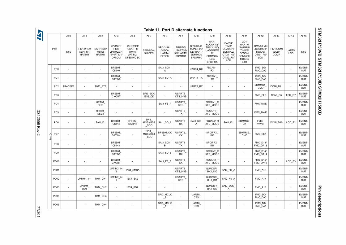
ST
M3
2H7
50V
B S
TM
32H
750
IB S
TM
32H
750
XB
Pin
de
scrip
tion
s
DS
1255
6 Rev 2
77/201
Table 11. Port D alternate functions
Port
AF0 AF1 AF2 AF3 AF4 AF5 AF6 AF7 AF8 AF9 AF10 AF11 AF12 AF13 AF14 AF15
SYSTIM1/2/16/17/LPTIM1/HRTIM1
SAI1/TIM3/4/5/12/
HRTIM1
LPUART/TIM8/
LPTIM2/3/4/5/HRTIM1/
DFSDM
I2C1/2/3/4/USART1/TIM15/
LPTIM2/DFSDM/CEC
SPI1/2/3/4/5/6/CEC
SPI2/3/SAI1/3/I2C4/UART4/DFSDM
SPI2/3/6/USART1/2/3/6/UART7/SDMMC1
SPI6/SAI2/4/UART4/5/8/LPUART/SDMMC1/SPDIFRX
SAI4/FDCAN1/2/TIM13/14/QUADSPI/FM
C/SDMMC2/
LCD/SPDIFRX
SAI2/4/TIM8/
QUADSPI/SDMMC2/OTG1_HS/OTG2_FS/
LCD
I2C4/UART7/
SWPMI1/TIM1/8/DFSDM/
SDMMC2/MDIOS/
ETH
TIM1/8/FMC/SDMMC1/
MDIOS/OTG1_FS/
LCD
TIM1/DCMI/LCD/COMP
UART5/LCD
SYSP
ort
D
PD0 - - -DFSDM_
CKIN6- -
SAI3_SCK_A
- UART4_RXFDCAN1_
RX- -
FMC_D2/FMC_DA2
- -EVENT-
OUT
PD1 - - -DFSDM_DATIN6
- - SAI3_SD_A - UART4_TXFDCAN1_
TX- -
FMC_D3/FMC_DA3
- -EVENT-
OUT
PD2 TRACED2 - TIM3_ETR - - - - - UART5_RX - - -SDMMC1_
CMDDCMI_D11 -
EVENT-OUT
PD3 - - -DFSDM_CKOUT
-SPI2_SCK/I2S2_CK
-USART2_CTS_NSS
- - - - FMC_CLK DCMI_D5 LCD_G7EVENT-
OUT
PD4 - -HRTIM_
FLT3- - - SAI3_FS_A
USART2_RTS
-FDCAN1_RXFD_MODE
- - FMC_NOE - -EVENT-
OUT
PD5 - -HRTIM_
EEV3- - - -
USART2_TX
-FDCAN1_TXFD_MODE
- - FMC_NWE - -EVENT-
OUT
PD6 - - SAI1_D1DFSDM_
CKIN4DFSDM_DATIN1
SPI3_MOSI/I2S3
_SDOSAI1_SD_A
USART2_RX
SAI4_SD_A
FDCAN2_RXFD_MODE
SAI4_D1SDMMC2_
CKFMC_NWAIT
DCMI_D10 LCD_B2EVENT-
OUT
PD7 - - -DFSDM_DATIN4
-SPI1_
MOSI/I2S1_SDO
DFSDM_CKIN1
USART2_CK
-SPDIFRX_
IN0-
SDMMC2_CMD
FMC_NE1 - -EVENT-
OUT
PD8 - - -DFSDM_
CKIN3- -
SAI3_SCK_B
USART3_TX
-SPDIFRX_
IN1- -
FMC_D13/FMC_DA13
- -EVENT-
OUT
PD9 - - -DFSDM_DATIN3
- - SAI3_SD_BUSART3_
RX-
FDCAN2_RXFD_MODE
- -FMC_D14/FMC_DA14
- -EVENT-
OUT
PD10 - - -DFSDM_CKOUT
- - SAI3_FS_BUSART3_
CK-
FDCAN2_TXFD_MODE
- -FMC_D15/FMC_DA15
- LCD_B3EVENT-
OUT
PD11 - - -LPTIM2_IN
2I2C4_SMBA - -
USART3_CTS_NSS
-QUADSPI_BK1_IO0
SAI2_SD_A - FMC_A16 - -EVENT-
OUT
PD12 - LPTIM1_IN1 TIM4_CH1LPTIM2_IN
1I2C4_SCL - -
USART3_RTS
-QUADSPI_BK1_IO1
SAI2_FS_A - FMC_A17 - -EVENT-
OUT
PD13 -LPTIM1_
OUTTIM4_CH2 - I2C4_SDA - - -
QUADSPI_BK1_IO3
SAI2_SCK_A
- FMC_A18 - -EVENT-
OUT
PD14 - - TIM4_CH3 - - -SAI3_MCLK
_B-
UART8_CTS
- - -FMC_D0/FMC_DA0
- -EVENT-
OUT
PD15 - - TIM4_CH4 - - -SAI3_MCLK
_A-
UART8_RTS
- - -FMC_D1/FMC_DA1
- -EVENT-
OUT
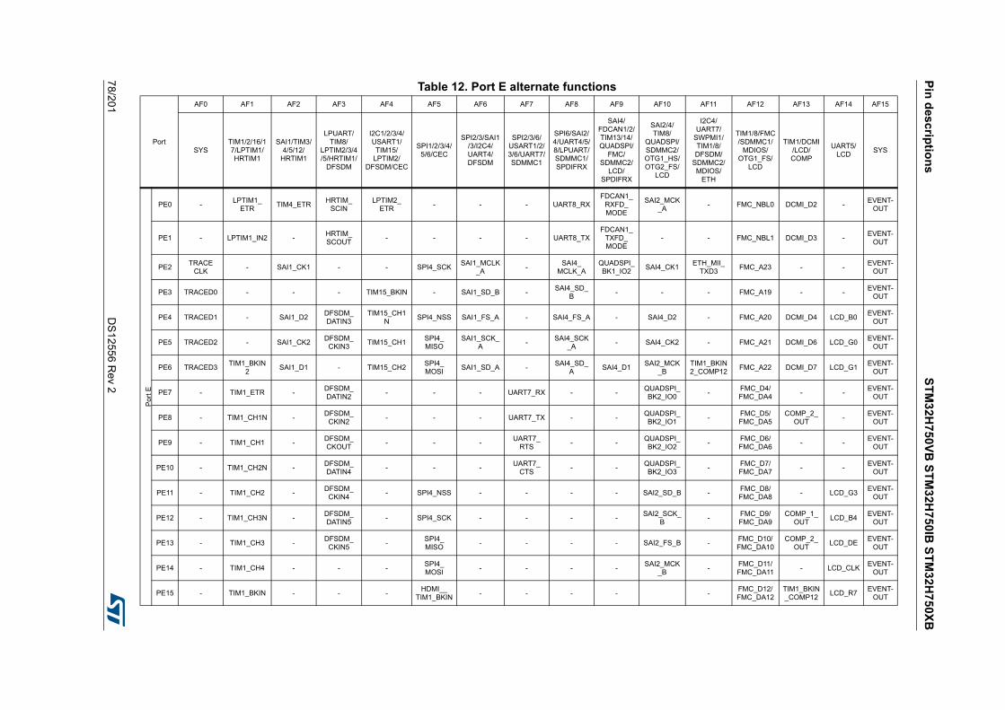
Pin
des
criptio
ns
ST
M3
2H
750
VB
ST
M3
2H75
0IB S
TM
32H
75
0XB
78/2
01D
S1
2556 R
ev 2
Table 12. Port E alternate functions
Port
AF0 AF1 AF2 AF3 AF4 AF5 AF6 AF7 AF8 AF9 AF10 AF11 AF12 AF13 AF14 AF15
SYSTIM1/2/16/17/LPTIM1/HRTIM1
SAI1/TIM3/4/5/12/
HRTIM1
LPUART/TIM8/
LPTIM2/3/4/5/HRTIM1/
DFSDM
I2C1/2/3/4/USART1/TIM15/
LPTIM2/DFSDM/CEC
SPI1/2/3/4/5/6/CEC
SPI2/3/SAI1/3/I2C4/UART4/DFSDM
SPI2/3/6/USART1/2/3/6/UART7/SDMMC1
SPI6/SAI2/4/UART4/5/8/LPUART/SDMMC1/SPDIFRX
SAI4/FDCAN1/2/TIM13/14/QUADSPI/
FMC/SDMMC2/
LCD/SPDIFRX
SAI2/4/TIM8/
QUADSPI/SDMMC2/OTG1_HS/OTG2_FS/
LCD
I2C4/UART7/
SWPMI1/TIM1/8/DFSDM/
SDMMC2/MDIOS/
ETH
TIM1/8/FMC/SDMMC1/
MDIOS/OTG1_FS/
LCD
TIM1/DCMI/LCD/COMP
UART5/LCD
SYSP
ort E
PE0 -LPTIM1_
ETRTIM4_ETR
HRTIM_SCIN
LPTIM2_ETR
- - - UART8_RXFDCAN1_
RXFD_MODE
SAI2_MCK_A
- FMC_NBL0 DCMI_D2 -EVENT-
OUT
PE1 - LPTIM1_IN2 -HRTIM_SCOUT
- - - - UART8_TXFDCAN1_
TXFD_MODE
- - FMC_NBL1 DCMI_D3 -EVENT-
OUT
PE2TRACE
CLK- SAI1_CK1 - - SPI4_SCK
SAI1_MCLK_A
-SAI4_
MCLK_AQUADSPI_BK1_IO2
SAI4_CK1ETH_MII_
TXD3FMC_A23 - -
EVENT-OUT
PE3 TRACED0 - - - TIM15_BKIN - SAI1_SD_B -SAI4_SD_
B- - - FMC_A19 - -
EVENT-OUT
PE4 TRACED1 - SAI1_D2DFSDM_DATIN3
TIM15_CH1N
SPI4_NSS SAI1_FS_A - SAI4_FS_A - SAI4_D2 - FMC_A20 DCMI_D4 LCD_B0EVENT-
OUT
PE5 TRACED2 - SAI1_CK2DFSDM_
CKIN3TIM15_CH1
SPI4_MISO
SAI1_SCK_A
-SAI4_SCK
_A- SAI4_CK2 - FMC_A21 DCMI_D6 LCD_G0
EVENT-OUT
PE6 TRACED3TIM1_BKIN
2SAI1_D1 - TIM15_CH2
SPI4_MOSI
SAI1_SD_A -SAI4_SD_
ASAI4_D1
SAI2_MCK_B
TIM1_BKIN2_COMP12
FMC_A22 DCMI_D7 LCD_G1EVENT-
OUT
PE7 - TIM1_ETR -DFSDM_DATIN2
- - - UART7_RX - -QUADSPI_BK2_IO0
-FMC_D4/FMC_DA4
- -EVENT-
OUT
PE8 - TIM1_CH1N -DFSDM_
CKIN2- - - UART7_TX - -
QUADSPI_BK2_IO1
-FMC_D5/FMC_DA5
COMP_2_OUT
-EVENT-
OUT
PE9 - TIM1_CH1 -DFSDM_CKOUT
- - -UART7_
RTS- -
QUADSPI_BK2_IO2
-FMC_D6/FMC_DA6
- -EVENT-
OUT
PE10 - TIM1_CH2N -DFSDM_DATIN4
- - -UART7_
CTS- -
QUADSPI_BK2_IO3
-FMC_D7/FMC_DA7
- -EVENT-
OUT
PE11 - TIM1_CH2 -DFSDM_
CKIN4- SPI4_NSS - - - - SAI2_SD_B -
FMC_D8/FMC_DA8
- LCD_G3EVENT-
OUT
PE12 - TIM1_CH3N -DFSDM_DATIN5
- SPI4_SCK - - - -SAI2_SCK_
B-
FMC_D9/FMC_DA9
COMP_1_OUT
LCD_B4EVENT-
OUT
PE13 - TIM1_CH3 -DFSDM_
CKIN5-
SPI4_MISO
- - - - SAI2_FS_B -FMC_D10/FMC_DA10
COMP_2_OUT
LCD_DEEVENT-
OUT
PE14 - TIM1_CH4 - - -SPI4_MOSI
- - - -SAI2_MCK
_B-
FMC_D11/FMC_DA11
- LCD_CLKEVENT-
OUT
PE15 - TIM1_BKIN - - -HDMI__
TIM1_BKIN- - - - -
FMC_D12/FMC_DA12
TIM1_BKIN_COMP12
LCD_R7EVENT-
OUT
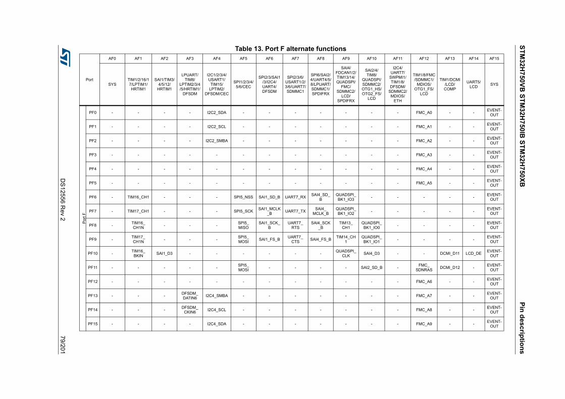
ST
M3
2H7
50V
B S
TM
32H
750
IB S
TM
32H
750
XB
Pin
de
scrip
tion
s
DS
1255
6 Rev 2
79/201
Table 13. Port F alternate functions
Port
AF0 AF1 AF2 AF3 AF4 AF5 AF6 AF7 AF8 AF9 AF10 AF11 AF12 AF13 AF14 AF15
SYSTIM1/2/16/17/LPTIM1/HRTIM1
SAI1/TIM3/4/5/12/
HRTIM1
LPUART/TIM8/
LPTIM2/3/4/5/HRTIM1/
DFSDM
I2C1/2/3/4/USART1/TIM15/
LPTIM2/DFSDM/CEC
SPI1/2/3/4/5/6/CEC
SPI2/3/SAI1/3/I2C4/UART4/DFSDM
SPI2/3/6/USART1/2/3/6/UART7/SDMMC1
SPI6/SAI2/4/UART4/5/8/LPUART/SDMMC1/SPDIFRX
SAI4/FDCAN1/2/TIM13/14/QUADSPI/
FMC/SDMMC2/
LCD/SPDIFRX
SAI2/4/TIM8/
QUADSPI/SDMMC2/OTG1_HS/OTG2_FS/
LCD
I2C4/UART7/
SWPMI1/TIM1/8/DFSDM/
SDMMC2/MDIOS/
ETH
TIM1/8/FMC/SDMMC1/
MDIOS/OTG1_FS/
LCD
TIM1/DCMI/LCD/COMP
UART5/LCD
SYSP
ort
F
PF0 - - - - I2C2_SDA - - - - - - - FMC_A0 - -EVENT-
OUT
PF1 - - - - I2C2_SCL - - - - - - - FMC_A1 - -EVENT-
OUT
PF2 - - - - I2C2_SMBA - - - - - - - FMC_A2 - -EVENT-
OUT
PF3 - - - - - - - - - - - - FMC_A3 - -EVENT-
OUT
PF4 - - - - - - - - - - - - FMC_A4 - -EVENT-
OUT
PF5 - - - - - - - - - - - - FMC_A5 - -EVENT-
OUT
PF6 - TIM16_CH1 - - - SPI5_NSS SAI1_SD_B UART7_RXSAI4_SD_
BQUADSPI_BK1_IO3
- - - - -EVENT-
OUT
PF7 - TIM17_CH1 - - - SPI5_SCKSAI1_MCLK
_BUART7_TX
SAI4_MCLK_B
QUADSPI_BK1_IO2
- - - - -EVENT-
OUT
PF8 -TIM16_CH1N
- - -SPI5_MISO
SAI1_SCK_B
UART7_RTS
SAI4_SCK_B
TIM13_CH1
QUADSPI_BK1_IO0
- - - -EVENT-
OUT
PF9 -TIM17_CH1N
- - -SPI5_MOSI
SAI1_FS_BUART7_
CTSSAI4_FS_B
TIM14_CH1
QUADSPI_BK1_IO1
- - - -EVENT-
OUT
PF10 -TIM16_BKIN
SAI1_D3 - - - - - -QUADSPI_
CLKSAI4_D3 - - DCMI_D11 LCD_DE
EVENT-OUT
PF11 - - - - -SPI5_MOSI
- - - - SAI2_SD_B -FMC_
SDNRASDCMI_D12 -
EVENT-OUT
PF12 - - - - - - - - - - - - FMC_A6 - -EVENT-
OUT
PF13 - - -DFSDM_DATIN6
I2C4_SMBA - - - - - - - FMC_A7 - -EVENT-
OUT
PF14 - - -DFSDM_
CKIN6I2C4_SCL - - - - - - - FMC_A8 - -
EVENT-OUT
PF15 - - - - I2C4_SDA - - - - - - - FMC_A9 - -EVENT-
OUT

Pin
des
criptio
ns
ST
M3
2H
750
VB
ST
M3
2H75
0IB S
TM
32H
75
0XB
80/2
01D
S1
2556 R
ev 2
Table 14. Port G alternate functions
Port
AF0 AF1 AF2 AF3 AF4 AF5 AF6 AF7 AF8 AF9 AF10 AF11 AF12 AF13 AF14 AF15
SYSTIM1/2/16/17/LPTIM1/HRTIM1
SAI1/TIM3/4/5/12/
HRTIM1
LPUART/TIM8/
LPTIM2/3/4/5/HRTIM1/
DFSDM
I2C1/2/3/4/USART1/TIM15/
LPTIM2/DFSDM/CEC
SPI1/2/3/4/5/6/CEC
SPI2/3/SAI1/3/I2C4/UART4/DFSDM
SPI2/3/6/USART1/2/3/6/UART7/SDMMC1
SPI6/SAI2/4/UART4/5/8/LPUART/SDMMC1/SPDIFRX
SAI4/FDCAN1/2/TIM13/14/QUADSPI/
FMC/SDMMC2/
LCD/SPDIFRX
SAI2/4/TIM8/QUADSPI/SDMMC2/OTG1_HS/OTG2_FS/
LCD
I2C4/UART7/SWPMI1/
TIM1/8/DFSDM/
SDMMC2/MDIOS/ETH
TIM1/8/FMC/SDMMC1/
MDIOS/OTG1_FS/
LCD
TIM1/DCMI/LCD
/COMP
UART5/LCD
SYSP
ort G
PG0 - - - - - - - - - - - - FMC_A10 - -EVENT-OUT
PG1 - - - - - - - - - - - - FMC_A11 - -EVENT-OUT
PG2 - - - TIM8_BKIN - - - - - - -TIM8_BKIN_
COMP12FMC_A12 - -
EVENT-OUT
PG3 - - -TIM8_BKIN2
- - - - - - -TIM8_BKIN2_COMP12
FMC_A13 - -EVENT-OUT
PG4 -TIM1_BKIN
2- - - - - - - - -
TIM1_BKIN2_COMP12
FMC_A14/FMC_BA0
- -EVENT-OUT
PG5 - TIM1_ETR - - - - - - - - - -FMC_A15/FMC_BA1
- -EVENT-OUT
PG6 -TIM17_BKIN
HRTIM_CHE1
- - - - - - -QUADSPI_BK1_NCS
- FMC_NE3DCMI_D1
2LCD_R
7EVENT-OUT
PG7 - -HRTIM_CHE2
- - -SAI1_
MCLK_AUSART6_
CK- - - - FMC_INT
DCMI_D13
LCD_CLK
EVENT-OUT
PG8 - - - TIM8_ETR - SPI6_NSS -USART6_
RTSSPDIFRX_
IN2- -
ETH_PPS_OUT
FMC_SDCLK
-LCD_
G7EVENT-OUT
PG9 - - - - -SPI1_
MISO/I2S1_SDI
-USART6_
RXSPDIFRX_
IN3QUADSPI_BK
2_IO2SAI2_FS_B -
FMC_NE2/FMC_NCE
DCMI_VSYNC
-EVENT-OUT
PG10 - -HRTIM_
FLT5- -
SPI1_NSS/I2S1_WS
- - - LCD_G3 SAI2_SD_B - FMC_NE3 DCMI_D2LCD_B
2EVENT-OUT
PG11 - -HRTIM_
EEV4- -
SPI1_SCK/I2S1_CK
- -SPDIFRX_
IN0- SDMMC2_D2
ETH_MII_TX_EN/
ETH_RMII_TX_EN
- DCMI_D3LCD_B
3EVENT-OUT
PG12 - LPTIM1_IN1HRTIM_
EEV5- -
SPI6_MISO
USART6_RTS
SPDIFRX_IN1
LCD_B4 -ETH_MII_
TXD1/ETH_RMII_TXD1
FMC_NE4 -LCD_
B1EVENT-OUT
PG13 TRACED0LPTIM1_
OUTHRTIM_EEV10
- - SPI6_SCK -USART6_CTS_NSS
- - -ETH_MII_
TXD0/ETH_RMII_TXD0
FMC_A24 -LCD_
R0EVENT-OUT

ST
M3
2H7
50V
B S
TM
32H
750
IB S
TM
32H
750
XB
Pin
de
scrip
tion
s
DS
1255
6 Rev 2
81/201
Por
t G
PG14 TRACED1LPTIM1_
ETR- - -
SPI6_MOSI
-USART6_
TXQUADSPI_BK2_IO3
-ETH_MII_
TXD1/ETH_RMII_TXD1
FMC_A25 -LCD_
B0EVENT-OUT
PG15 - - - - - - -USART6_CTS_NSS
- - - -FMC_
SDNCASDCMI_
D13-
EVENT-OUT
Table 14. Port G alternate functions (continued)
Port
AF0 AF1 AF2 AF3 AF4 AF5 AF6 AF7 AF8 AF9 AF10 AF11 AF12 AF13 AF14 AF15
SYSTIM1/2/16/17/LPTIM1/HRTIM1
SAI1/TIM3/4/5/12/
HRTIM1
LPUART/TIM8/
LPTIM2/3/4/5/HRTIM1/
DFSDM
I2C1/2/3/4/USART1/TIM15/
LPTIM2/DFSDM/CEC
SPI1/2/3/4/5/6/CEC
SPI2/3/SAI1/3/I2C4/UART4/DFSDM
SPI2/3/6/USART1/2/3/6/UART7/SDMMC1
SPI6/SAI2/4/UART4/5/8/LPUART/SDMMC1/SPDIFRX
SAI4/FDCAN1/2/TIM13/14/QUADSPI/
FMC/SDMMC2/
LCD/SPDIFRX
SAI2/4/TIM8/QUADSPI/SDMMC2/OTG1_HS/OTG2_FS/
LCD
I2C4/UART7/SWPMI1/
TIM1/8/DFSDM/
SDMMC2/MDIOS/ETH
TIM1/8/FMC/SDMMC1/
MDIOS/OTG1_FS/
LCD
TIM1/DCMI/LCD
/COMP
UART5/LCD
SYS
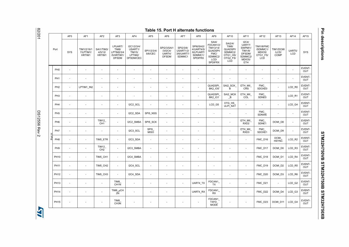
Pin
des
criptio
ns
ST
M3
2H
750
VB
ST
M3
2H75
0IB S
TM
32H
75
0XB
82/2
01D
S1
2556 R
ev 2
Table 15. Port H alternate functions
Port
AF0 AF1 AF2 AF3 AF4 AF5 AF6 AF7 AF8 AF9 AF10 AF11 AF12 AF13 AF14 AF15
SYSTIM1/2/16/17/LPTIM1/HRTIM1
SAI1/TIM3/4/5/12/
HRTIM1
LPUART/TIM8/
LPTIM2/3/4/5/HRTIM1/
DFSDM
I2C1/2/3/4/USART1/TIM15/
LPTIM2/DFSDM/CEC
SPI1/2/3/4/5/6/CEC
SPI2/3/SAI1/3/I2C4/UART4/DFSDM
SPI2/3/6/USART1/2/3/6/UART7/SDMMC1
SPI6/SAI2/4/UART4/5/8/LPUART/SDMMC1/SPDIFRX
SAI4/FDCAN1/2/TIM13/14/QUADSPI/
FMC/SDMMC2/
LCD/SPDIFRX
SAI2/4/TIM8/
QUADSPI/SDMMC2/OTG1_HS/OTG2_FS/
LCD
I2C4/UART7/
SWPMI1/TIM1/8/DFSDM/
SDMMC2/MDIOS/
ETH
TIM1/8/FMC/SDMMC1/
MDIOS/OTG1_FS/
LCD
TIM1/DCMI/LCD/COMP
UART5/LCD
SYSP
ort
H
PH0 - - - - - - - - - - - - - - -EVENT-
OUT
PH1 - - - - - - - - - - - - - - -EVENT-
OUT
PH2 - LPTIM1_IN2 - - - - - - -QUADSPI_BK2_IO0
SAI2_SCK_B
ETH_MII_CRS
FMC_SDCKE0
- LCD_R0EVENT-
OUT
PH3 - - - - - - - - -QUADSPI_BK2_IO1
SAI2_MCK_B
ETH_MII_COL
FMC_SDNE0
- LCD_R1EVENT-
OUT
PH4 - - - - I2C2_SCL - - - - LCD_G5OTG_HS_ULPI_NXT
- - - LCD_G4EVENT-
OUT
PH5 - - - - I2C2_SDA SPI5_NSS - - - - - -FMC_
SDNWE- -
EVENT-OUT
PH6 - -TIM12_
CH1- I2C2_SMBA SPI5_SCK - - - - -
ETH_MII_RXD2
FMC_SDNE1
DCMI_D8 -EVENT-
OUT
PH7 - - - - I2C3_SCLSPI5_MISO
- - - - -ETH_MII_
RXD3FMC_
SDCKE1DCMI_D9 -
EVENT-OUT
PH8 - - TIM5_ETR - I2C3_SDA - - - - - - - FMC_D16DCMI_HSYNC
LCD_R2EVENT-
OUT
PH9 - -TIM12_
CH2- I2C3_SMBA - - - - - - - FMC_D17 DCMI_D0 LCD_R3
EVENT-OUT
PH10 - - TIM5_CH1 - I2C4_SMBA - - - - - - - FMC_D18 DCMI_D1 LCD_R4EVENT-
OUT
PH11 - - TIM5_CH2 - I2C4_SCL - - - - - - - FMC_D19 DCMI_D2 LCD_R5EVENT-
OUT
PH12 - - TIM5_CH3 - I2C4_SDA - - - - - - - FMC_D20 DCMI_D3 LCD_R6EVENT-
OUT
PH13 - - -TIM8_CH1N
- - - - UART4_TXFDCAN1_
TX- - FMC_D21 - LCD_G2
EVENT-OUT
PH14 - - -TIM8_µCH
2N- - - - UART4_RX
FDCAN1_RX
- - FMC_D22 DCMI_D4 LCD_G3EVENT-
OUT
PH15 - - -TIM8_CH3N
- - - - -FDCAN1_
TXFD_MODE
- - FMC_D23 DCMI_D11 LCD_G4EVENT-
OUT

ST
M3
2H7
50V
B S
TM
32H
750
IB S
TM
32H
750
XB
Pin
de
scrip
tion
s
DS
1255
6 Rev 2
83/201
Table 16. Port I alternate functions
Port
AF0 AF1 AF2 AF3 AF4 AF5 AF6 AF7 AF8 AF9 AF10 AF11 AF12 AF13 AF14 AF15
SYSTIM1/2/16/17/LPTIM1/HRTIM1
SAI1/TIM3/4/5/12/
HRTIM1
LPUART/TIM8/
LPTIM2/3/4/5/HRTIM1/
DFSDM
I2C1/2/3/4/USART1/TIM15/
LPTIM2/DFSDM/CEC
SPI1/2/3/4/5/6/CEC
SPI2/3/SAI1/3/I2C4/UART4/DFSDM
SPI2/3/6/USART1/2/3/6/UART7/SDMMC1
SPI6/SAI2/4/UART4/5/8/LPUART/SDMMC1/SPDIFRX
SAI4/FDCAN1/2/TIM13/14/QUADSPI/
FMC/SDMMC2/
LCD/SPDIFRX
SAI2/4/TIM8/
QUADSPI/SDMMC2/OTG1_HS/OTG2_FS/
LCD
I2C4/UART7/
SWPMI1/TIM1/8/DFSDM/
SDMMC2/MDIOS/
ETH
TIM1/8/FMC/SDMMC1/
MDIOS/OTG1_FS/
LCD
TIM1/DCMI/LCD/COMP
UART5/LCD
SYSP
ort
I
PI0 - - TIM5_CH4 - -SPI2_NSS/I2S2_WS
- - -FDCAN1_
RXFD_MODE
- - FMC_D24 DCMI_D13 LCD_G5EVENT-
OUT
PI1 - - -TIM8_BKIN
2-
SPI2_SCK/I2S2_CK
- - - - -TIM8_BKIN2_COMP12
FMC_D25 DCMI_D8 LCD_G6EVENT-
OUT
PI2 - - - TIM8_CH4 -SPI2_
MISO/I2S2_SDI
- - - - - - FMC_D26 DCMI_D9 LCD_G7EVENT-
OUT
PI3 - - - TIM8_ETR -SPI2_
MOSI/I2S2_SDO
- - - - - - FMC_D27 DCMI_D10 -EVENT-
OUT
PI4 - - - TIM8_BKIN - - - - - -SAI2_MCK
_ATIM8_BKIN_COMP12
FMC_NBL2 DCMI_D5 LCD_B4EVENT-
OUT
PI5 - - - TIM8_CH1 - - - - - -SAI2_SCK_
A- FMC_NBL3
DCMI_VSYNC
LCD_B5EVENT-
OUT
PI6 - - - TIM8_CH2 - - - - - - SAI2_SD_A - FMC_D28 DCMI_D6 LCD_B6EVENT-
OUT
PI7 - - - TIM8_CH3 - - - - - - SAI2_FS_A - FMC_D29 DCMI_D7 LCD_B7EVENT-
OUT
PI8 - - - - - - - - - - - - - - -EVENT-
OUT
PI9 - - - - - - - - UART4_RXFDCAN1_
RX- - FMC_D30 -
LCD_VSYNC
EVENT-OUT
PI10 - - - - - - - - -FDCAN1_
RXFD_MODE
-ETH_MII_
RX_ERFMC_D31 -
LCD_HSYNC
EVENT-OUT
PI11 - - - - - - - - - LCD_G6OTG_HS_ULPI_DIR
- - - -EVENT-
OUT
PI12 - - - - - - - - - - -ETH_TX_
ER- -
LCD_HSYNC
EVENT-OUT
PI13 - - - - - - - - - - - - - -LCD_
VSYNCEVENT-
OUT
PI14 - - - - - - - - - - - - - - LCD_CLKEVENT-
OUT
PI15 - - - - - - - - - LCD_G2 - - - - LCD_R0EVENT-
OUT

Pin
des
criptio
ns
ST
M3
2H
750
VB
ST
M3
2H75
0IB S
TM
32H
75
0XB
84/2
01D
S1
2556 R
ev 2
Table 17. Port J alternate functions
Port
AF0 AF1 AF2 AF3 AF4 AF5 AF6 AF7 AF8 AF9 AF10 AF11 AF12 AF13 AF14 AF15
SYSTIM1/2/16/17/LPTIM1/HRTIM1
SAI1/TIM3/4/5/12/
HRTIM1
LPUART/TIM8/
LPTIM2/3/4/5/HRTIM1/
DFSDM
I2C1/2/3/4/USART1/TIM15/
LPTIM2/DFSDM/CEC
SPI1/2/3/4/5/6/CEC
SPI2/3/SAI1/3/I2C4/UART4/DFSDM
SPI2/3/6/USART1/2/3/6/UART7/SDMMC1
SPI6/SAI2/4/UART4/5/8/LPUART/SDMMC1/SPDIFRX
SAI4/FDCAN1/2/TIM13/14/QUADSPI/
FMC/SDMMC2/
LCD/SPDIFRX
SAI2/4/TIM8/
QUADSPI/SDMMC2/OTG1_HS/OTG2_FS/
LCD
I2C4/UART7/
SWPMI1/TIM1/8/DFSDM/
SDMMC2/MDIOS/
ETH
TIM1/8/FMC/SDMMC1/
MDIOS/OTG1_FS/
LCD
TIM1/DCMI/LCD/COMP
UART5/LCD
SYSP
ort J
PJ0 - - - - - - - - - LCD_R7 - - - - LCD_R1EVENT-
OUT
PJ1 - - - - - - - - - - - - - - LCD_R2EVENT-
OUT
PJ2 - - - - - - - - - - - - - - LCD_R3EVENT-
OUT
PJ3 - - - - - - - - - - - - - - LCD_R4EVENT-
OUT
PJ4 - - - - - - - - - - - - - - LCD_R5EVENT-
OUT
PJ5 - - - - - - - - - - - - - - LCD_R6EVENT-
OUT
PJ6 - - - TIM8_CH2 - - - - - - - - - - LCD_R7EVENT-
OUT
PJ7 TRGIN - -TIM8_CH2N
- - - - - - - - - - LCD_G0EVENT-
OUT
PJ8 - TIM1_CH3N - TIM8_CH1 - - - - UART8_TX - - - - - LCD_G1EVENT-
OUT
PJ9 - TIM1_CH3 -TIM8_CH1N
- - - - UART8_RX - - - - - LCD_G2EVENT-
OUT
PJ10 - TIM1_CH2N - TIM8_CH2 -SPI5_MOSI
- - - - - - - - LCD_G3EVENT-
OUT
PJ11 - TIM1_CH2 -TIM8_CH2N
-SPI5_MISO
- - - - - - - - LCD_G4EVENT-
OUT
PJ12 TRGOUT - - - - - - - - LCD_G3 - - - - LCD_B0EVENT-
OUT
PJ13 - - - - - - - - - LCD_B4 - - - - LCD_B1EVENT-
OUT
PJ14 - - - - - - - - - - - - - - LCD_B2EVENT-
OUT
PJ15 - - - - - - - - - - - - - - LCD_B3EVENT-
OUT

ST
M3
2H7
50V
B S
TM
32H
750
IB S
TM
32H
750
XB
Pin
de
scrip
tion
s
DS
1255
6 Rev 2
85/201
Table 18. Port K alternate functions
Port
AF0 AF1 AF2 AF3 AF4 AF5 AF6 AF7 AF8 AF9 AF10 AF11 AF12 AF13 AF14 AF15
SYSTIM1/2/16/17/LPTIM1/HRTIM1
SAI1/TIM3/4/5/12/
HRTIM1
LPUART/TIM8/
LPTIM2/3/4/5/HRTIM1/
DFSDM
I2C1/2/3/4/USART1/TIM15/
LPTIM2/DFSDM/CEC
SPI1/2/3/4/5/6/CEC
SPI2/3/SAI1/3/I2C4/UART4/DFSDM
SPI2/3/6/USART1/2/3/6/UART7/SDMMC1
SPI6/SAI2/4/UART4/5/8/LPUART/SDMMC1/SPDIFRX
SAI4/FDCAN1/2/TIM13/14/QUADSPI/
FMC/SDMMC2/
LCD/SPDIFRX
SAI2/4/TIM8/
QUADSPI/SDMMC2/OTG1_HS/OTG2_FS/
LCD
I2C4/UART7/
SWPMI1/TIM1/8/DFSDM/
SDMMC2/MDIOS/
ETH
TIM1/8/FMC/SDMMC1/
MDIOS/OTG1_FS/
LCD
TIM1/DCMI/LCD/COMP
UART5/LCD
SYSP
ort
K
PK0 - TIM1_CH1N - TIM8_CH3 - SPI5_SCK - - - - - - - - LCD_G5EVENT-
OUT
PK1 - TIM1_CH1 -TIM8_CH3N
- SPI5_NSS - - - - - - - - LCD_G6EVENT-
OUT
PK2 - TIM1_BKIN - TIM8_BKIN - - - - - -TIM8_BKIN_COMP12
TIM1_BKIN_COMP12
- - LCD_G7EVENT-
OUT
PK3 - - - - - - - - - - - - - - LCD_B4EVENT-
OUT
PK4 - - - - - - - - - - - - - - LCD_B5EVENT-
OUT
PK5 - - - - - - - - - - - - - - LCD_B6EVENT-
OUT
PK6 - - - - - - - - - - - - - - LCD_B7EVENT-
OUT
PK7 - - - - - - - - - - - - - - LCD_DEEVENT-
OUT
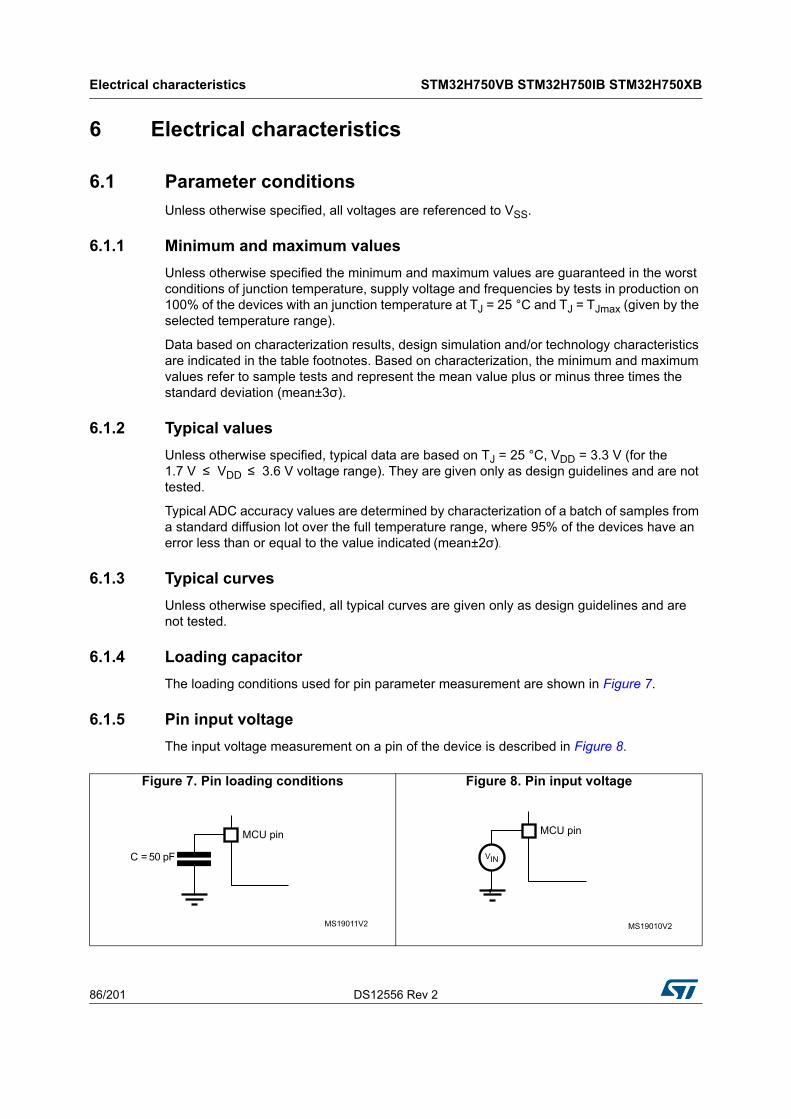
Electrical characteristics STM32H750VB STM32H750IB STM32H750XB
86/201 DS12556 Rev 2
6 Electrical characteristics
6.1 Parameter conditions
Unless otherwise specified, all voltages are referenced to VSS.
6.1.1 Minimum and maximum values
Unless otherwise specified the minimum and maximum values are guaranteed in the worst conditions of junction temperature, supply voltage and frequencies by tests in production on 100% of the devices with an junction temperature at TJ = 25 °C and TJ = TJmax (given by the selected temperature range).
Data based on characterization results, design simulation and/or technology characteristics are indicated in the table footnotes. Based on characterization, the minimum and maximum values refer to sample tests and represent the mean value plus or minus three times the standard deviation (mean±3σ).
6.1.2 Typical values
Unless otherwise specified, typical data are based on TJ = 25 °C, VDD = 3.3 V (for the 1.7 V ≤ VDD ≤ 3.6 V voltage range). They are given only as design guidelines and are not tested.
Typical ADC accuracy values are determined by characterization of a batch of samples from a standard diffusion lot over the full temperature range, where 95% of the devices have an error less than or equal to the value indicated (mean±2σ).
6.1.3 Typical curves
Unless otherwise specified, all typical curves are given only as design guidelines and are not tested.
6.1.4 Loading capacitor
The loading conditions used for pin parameter measurement are shown in Figure 7.
6.1.5 Pin input voltage
The input voltage measurement on a pin of the device is described in Figure 8.
Figure 7. Pin loading conditions Figure 8. Pin input voltage
MS19011V2
C = 50 pF
MCU pin
MS19010V2
MCU pin
VIN
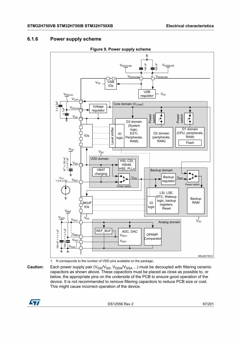
DS12556 Rev 2 87/201
STM32H750VB STM32H750IB STM32H750XB Electrical characteristics
189
6.1.6 Power supply scheme
Figure 9. Power supply scheme
1. N corresponds to the number of VDD pins available on the package..
Caution: Each power supply pair (VDD/VSS, VDDA/VSSA ...) must be decoupled with filtering ceramic capacitors as shown above. These capacitors must be placed as close as possible to, or below, the appropriate pins on the underside of the PCB to ensure good operation of the device. It is not recommended to remove filtering capacitors to reduce PCB size or cost. This might cause incorrect operation of the device.
MSv46116V3
BKUP IOs
VDD domain
Analog domain
Core domain (VCORE)
Backup domain
D3 domain(System
logic,EXTI,
Peripherals,RAM)
D1 domain(CPU, peripherals,
RAM)
Leve
l shi
fter
OPAMP, Comparator
Voltageregulator
ADC, DAC
Flash
D2 domain(peripherals,
RAM)
Pow
er
switc
h
Power switch
VCAP
VSS
VDDLDO
VBAT
VDDA
VREF+
VREF-
VSSA
Backupregulator
VDD
Backup RAM
Power switch
HSI, CSI, HSI48,
HSE, PLLs
IOs
Pow
er
switc
h
USBregulator
VDD50USBVDD33USB
VSS
VSS
VSS
REF_BUF
VSS
IOlogic
VREF+
USBIOs
VSS
VSW
LSI, LSE, RTC, Wakeup logic, backup
registers, Reset
IOlogic
VBKP
VBATcharging
VREF-
VDDA
VBAT1.2 to 3.6V
2 x
2.2μ
F
N(1
) x 1
00 n
F +
1 x
4.7
μF
100
nF
100
nF +
1 x
1 μ
F
4..7
μF
100
nF
VDD
VDDLDO
100
nF +
1 x
1 μ
F
VREF
VDD33USB VDD50USB

Electrical characteristics STM32H750VB STM32H750IB STM32H750XB
88/201 DS12556 Rev 2
6.1.7 Current consumption measurement
Figure 10. Current consumption measurement scheme
6.2 Absolute maximum ratings
Stresses above the absolute maximum ratings listed in Table 19: Voltage characteristics, Table 20: Current characteristics, and Table 21: Thermal characteristics may cause permanent damage to the device. These are stress ratings only and the functional operation of the device at these conditions is not implied. Exposure to maximum rating conditions for extended periods may affect device reliability.
ai14126
VBAT
VDD
VDDA
IDD_VBAT
IDD
Table 19. Voltage characteristics (1)
1. All main power (VDD, VDDA, VDD33USB, VBAT) and ground (VSS, VSSA) pins must always be connected to the external power supply, in the permitted range.
Symbols Ratings Min Max Unit
VDDX - VSSExternal main supply voltage (including VDD, VDDLDO, VDDA, VDD33USB, VBAT)
−0.3 4.0 V
VIN(2)
2. VIN maximum must always be respected. Refer to Table 57 for the maximum allowed injected current values.
Input voltage on FT_xxx pins VSS−0.3Min(VDD, VDDA, VDD33USB, VBAT)
+4.0(3)(4)
3. This formula has to be applied on power supplies related to the IO structure described by the pin definition table.
4. To sustain a voltage higher than 4V the internal pull-up/pull-down resistors must be disabled.
V
Input voltage on TT_xx pins VSS-0.3 4.0 V
Input voltage on BOOT0 pin VSS 9.0 V
Input voltage on any other pins VSS-0.3 4.0 V
|∆VDDX|Variations between different VDDX power pins of the same domain
- 50 mV
|VSSx-VSS| Variations between all the different ground pins - 50 mV
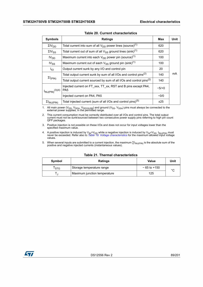
DS12556 Rev 2 89/201
STM32H750VB STM32H750IB STM32H750XB Electrical characteristics
189
Table 20. Current characteristics
Symbols Ratings Max Unit
ΣIVDD Total current into sum of all VDD power lines (source)(1)
1. All main power (VDD, VDDA, VDD33USB) and ground (VSS, VSSA) pins must always be connected to the external power supplies, in the permitted range.
620
mA
ΣIVSS Total current out of sum of all VSS ground lines (sink)(1) 620
IVDD Maximum current into each VDD power pin (source)(1) 100
IVSS Maximum current out of each VSS ground pin (sink)(1) 100
IIO Output current sunk by any I/O and control pin 20
ΣI(PIN)
Total output current sunk by sum of all I/Os and control pins(2)
2. This current consumption must be correctly distributed over all I/Os and control pins. The total output current must not be sunk/sourced between two consecutive power supply pins referring to high pin count QFP packages.
140
Total output current sourced by sum of all I/Os and control pins(2) 140
IINJ(PIN)(3)(4)
3. Positive injection is not possible on these I/Os and does not occur for input voltages lower than the specified maximum value.
4. A positive injection is induced by VIN>VDD while a negative injection is induced by VIN<VSS. IINJ(PIN) must never be exceeded. Refer also to Table 19: Voltage characteristics for the maximum allowed input voltage values.
Injected current on FT_xxx, TT_xx, RST and B pins except PA4, PA5
−5/+0
Injected current on PA4, PA5 −0/0
ΣIINJ(PIN) Total injected current (sum of all I/Os and control pins)(5)
5. When several inputs are submitted to a current injection, the maximum ∑IINJ(PIN) is the absolute sum of the positive and negative injected currents (instantaneous values).
±25
Table 21. Thermal characteristics
Symbol Ratings Value Unit
TSTG Storage temperature range − 65 to +150°C
TJ Maximum junction temperature 125

Electrical characteristics STM32H750VB STM32H750IB STM32H750XB
90/201 DS12556 Rev 2
6.3 Operating conditions
6.3.1 General operating conditions
Table 22. General operating conditions
Symbol Parameter Operating conditions Min Max Unit
VDD Standard operating voltage - 1.62(1) 3.6
V
VDDLDO Supply voltage for the internal regulator VDDLDO ≤ VDD 1.62(1) 3.6
VDD33USB Standard operating voltage, USB domainUSB used 3.0 3.6
USB not used 0 3.6
VDDA Analog operating voltage
ADC or COMP used 1.62
3.6
DAC used 1.8
OPAMP used 2.0
VREFBUF used 1.8
ADC, DAC, OPAMP, COMP, VREFBUF not
used0
VIN I/O Input voltage
TT_xx I/O −0.3 VDD+0.3
BOOT0 0 9
All I/O except BOOT0 and TT_xx
−0.3Min(VDD, VDDA,
VDD33USB) +3.6V < 5.5V(2)(3)
PDPower dissipation at TA = 85 °C for suffix 6(4)
TFBGA240+25 - - 1093
mWUFBGA176+25 - - 1070
LQFP100 - - 889
TA Ambient temperature for the suffix 6 version
Maximum power dissipation –40 85°C
Low-power dissipation(5) –40 105
TJ Junction temperature range
Suffix 6 version –40 125 °C
1. When RESET is released functionality is guaranteed down to VBOR0 min
2. This formula has to be applied on power supplies related to the IO structure described by the pin definition table.
3. For operation with voltage higher than Min (VDD, VDDA, VDD33USB) +0.3V, the internal Pull-up and Pull-Down resistors must be disabled.
4. If TA is lower, higher PD values are allowed as long as TJ does not exceed TJmax (see Section 7.4: Thermal characteristics).
5. In low-power dissipation state, TA can be extended to this range as long as TJ does not exceed TJmax (see Section 7.4: Thermal characteristics).
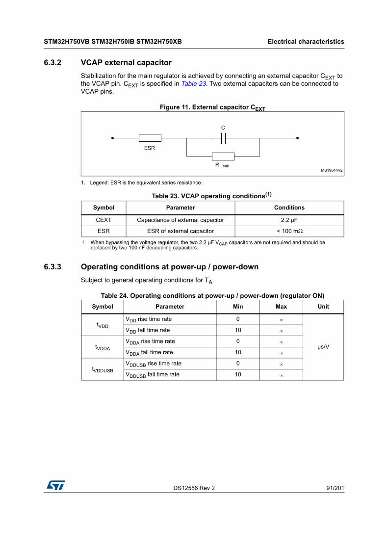
DS12556 Rev 2 91/201
STM32H750VB STM32H750IB STM32H750XB Electrical characteristics
189
6.3.2 VCAP external capacitor
Stabilization for the main regulator is achieved by connecting an external capacitor CEXT to the VCAP pin. CEXT is specified in Table 23. Two external capacitors can be connected to VCAP pins.
Figure 11. External capacitor CEXT
1. Legend: ESR is the equivalent series resistance.
6.3.3 Operating conditions at power-up / power-down
Subject to general operating conditions for TA.
Table 24. Operating conditions at power-up / power-down (regulator ON)
Table 23. VCAP operating conditions(1)
1. When bypassing the voltage regulator, the two 2.2 µF VCAP capacitors are not required and should be replaced by two 100 nF decoupling capacitors.
Symbol Parameter Conditions
CEXT Capacitance of external capacitor 2.2 µF
ESR ESR of external capacitor < 100 mΩ
MS19044V2
ESR
R Leak
C
Symbol Parameter Min Max Unit
tVDD
VDD rise time rate 0 ∞
µs/V
VDD fall time rate 10 ∞
tVDDA
VDDA rise time rate 0 ∞
VDDA fall time rate 10 ∞
tVDDUSB
VDDUSB rise time rate 0 ∞VDDUSB fall time rate 10 ∞
Electrical characteristics STM32H750VB STM32H750IB STM32H750XB
92/201 DS12556 Rev 2
6.3.4 Embedded reset and power control block characteristics
The parameters given in Table 25 are derived from tests performed under ambient temperature and VDD supply voltage conditions summarized in Table 22: General operating conditions.
Table 25. Reset and power control block characteristics
Symbol Parameter Conditions Min Typ Max Unit
tRSTTEMPO(1) Reset temporization
after BOR0 released- - 377 - µs
VBOR0 Brown-out reset threshold 0Rising edge(1) 1.62 1.67 1.71
V
Falling edge 1.58 1.62 1.68
VBOR1 Brown-out reset threshold 1Rising edge 2.04 2.10 2.15
Falling edge 1.95 2.00 2.06
VBOR2 Brown-out reset threshold 2Rising edge 2.34 2.41 2.47
Falling edge 2.25 2.31 2.37
VBOR3 Brown-out reset threshold 3Rising edge 2.63 2.70 2.78
Falling edge 2.54 2.61 2.68
VPVD0Programmable Voltage
Detector threshold 0
Rising edge 1.90 1.96 2.01
Falling edge 1.81 1.86 1.91
VPVD1Programmable Voltage
Detector threshold 1
Rising edge 2.05 2.10 2.16
Falling edge 1.96 2.01 2.06
VPVD2Programmable Voltage
Detector threshold 2
Rising edge 2.19 2.26 2.32
Falling edge 2.10 2.15 2.21
VPVD3Programmable Voltage
Detector threshold 3
Rising edge 2.35 2.41 2.47
Falling edge 2.25 2.31 2.37
VPVD4Programmable Voltage
Detector threshold 4
Rising edge 2.49 2.56 2.62
Falling edge 2.39 2.45 2.51
VPVD5Programmable Voltage
Detector threshold 5
Rising edge 2.64 2.71 2.78
Falling edge 2.55 2.61 2.68
VPVD6Programmable Voltage
Detector threshold 6
Rising edge 2.78 2.86 2.94
Falling edge in Run mode 2.69 2.76 2.83
Vhyst_BOR_PVDHysteresis voltage of BOR (unless BOR0) and PVD
Hysteresis in Run mode - 100 - mV
IDD_BOR_PVD(1) BOR(2) (unless BOR0) and
PVD consumption from VDD- - 0.630 µA

DS12556 Rev 2 93/201
STM32H750VB STM32H750IB STM32H750XB Electrical characteristics
189
6.3.5 Embedded reference voltage
The parameters given in Table 26 are derived from tests performed under ambient temperature and VDD supply voltage conditions summarized in Table 22: General operating conditions.
VAVM_0Analog voltage detector for
VDDA threshold 0
Rising edge 1.66 1.71 1.76
V
Falling edge 1.56 1.61 1.66
VAVM_1Analog voltage detector for
VDDA threshold 1
Rising edge 2.06 2.12 2.19
Falling edge 1.96 2.02 2.08
VAVM_2Analog voltage detector for
VDDA threshold 2
Rising edge 2.42 2.50 2.58
Falling edge 2.35 2.42 2.49
VAVM_3Analog voltage detector for
VDDA threshold 3
Rising edge 2.74 2.83 2.91
Falling edge 2.64 2.72 2.80
Vhyst_VDDAHysteresis of VDDA voltage
detector- - 100 - mV
IDD_PVMPVM consumption from
VDD(1)- - - 0.25 µA
IDD_VDDAVoltage detector
consumption on VDDA(1) Resistor bridge - - 2.5 µA
1. Guaranteed by design.
2. BOR0 is enabled in all modes and its consumption is therefore included in the supply current characteristics tables (refer to Section 6.3.6: Supply current characteristics).
Table 25. Reset and power control block characteristics (continued)
Symbol Parameter Conditions Min Typ Max Unit
Table 26. Embedded reference voltage
Symbol Parameter Conditions Min Typ Max Unit
VREFINT Internal reference voltages-40°C < TJ < 105°C,
VDD = 3.3 V1.180 1.216 1.255 V
tS_vrefint(1)(2)
ADC sampling time when reading the internal reference voltage
- 4.3 - -
µs
tS_vbat(1)(2)
VBAT sampling time when reading the internal VBAT reference voltage
- 9 - -
Irefbuf(2) Reference Buffer
consumption for ADCVDDA=3.3 V 9 13.5 23 µA
ΔVREFINT(2)
Internal reference voltage spread over the temperature range
-40°C < TJ < 105°C - 5 15 mV
Tcoeff(2) Average temperature
coefficientAverage temperature
coefficient- 20 70 ppm/°C
VDDcoeff(2) Average Voltage coefficient 3.0V < VDD < 3.6V - 10 1370 ppm/V

Electrical characteristics STM32H750VB STM32H750IB STM32H750XB
94/201 DS12556 Rev 2
6.3.6 Supply current characteristics
The current consumption is a function of several parameters and factors such as the operating voltage, ambient temperature, I/O pin loading, device software configuration, operating frequencies, I/O pin switching rate, program location in memory and executed binary code.
The current consumption is measured as described in Figure 10: Current consumption measurement scheme.
All the run-mode current consumption measurements given in this section are performed with a CoreMark code.
Typical and maximum current consumption
The MCU is placed under the following conditions:
• All I/O pins are in analog input mode.
• All peripherals are disabled except when explicitly mentioned.
• The Flash memory access time is adjusted with the minimum wait states number, depending on the fACLK frequency (refer to the table “Number of wait states according to CPU clock (frcc_c_ck) frequency and VCORE range” available in the reference manual).
• When the peripherals are enabled, the AHB clock frequency is the CPU frequency divided by 2 and the APB clock frequency is AHB clock frequency divided by 2.
The parameters given in Table 28 to Table 36 are derived from tests performed under ambient temperature and supply voltage conditions summarized in Table 22: General operating conditions.
VREFINT_DIV1 1/4 reference voltage - - 25 -%
VREFINTVREFINT_DIV2 1/2 reference voltage - - 50 -
VREFINT_DIV3 3/4 reference voltage - - 75 -
1. The shortest sampling time for the application can be determined by multiple iterations.
2. Guaranteed by design.
Table 26. Embedded reference voltage (continued)
Symbol Parameter Conditions Min Typ Max Unit
Table 27. Internal reference voltage calibration values
Symbol Parameter Memory address
VREFIN_CAL Raw data acquired at temperature of 30 °C, VDDA = 3.3 V 1FF1E860 - 1FF1E861

DS12556 Rev 2 95/201
STM32H750VB STM32H750IB STM32H750XB Electrical characteristics
189
Table 28. Typical and maximum current consumption in Run mode, code with data processingrunning from ITCM, regulator ON(1)
Symbol Parameter Conditionsfrcc_c_ck (MHz)
Typ
Max(2)
unitTJ = 25°C
TJ = 85°C
TJ = 105°C
TJ = 125°C
IDD
Supply current in Run
mode
All peripherals
disabled
VOS1400 71 110 210 290 540
mA
300 56 - - - -
VOS2
300 50 72 170 230 370
216 37 58 150 210 380
200 35.5 - - - -
VOS3
200 33 50 130 190 300
180 30 47 130 180 290
168 28 45 130 180 290
144 25 41 120 180 290
60 13 28 110 160 280
25 10 24 99 160 270
All peripherals
enabled
VOS1400 165 220(3) 400 500(3) 840
300 130 - - - -
VOS2300 120 170 300 390 570
200 83 - - - -
VOS3 200 78 110 220 300 470
1. Data are in DTCM for best computation performance, cache has no influence on consumption in this case.
2. Guaranteed by characterization results unless otherwise specified.
3. Guaranteed by test in production.
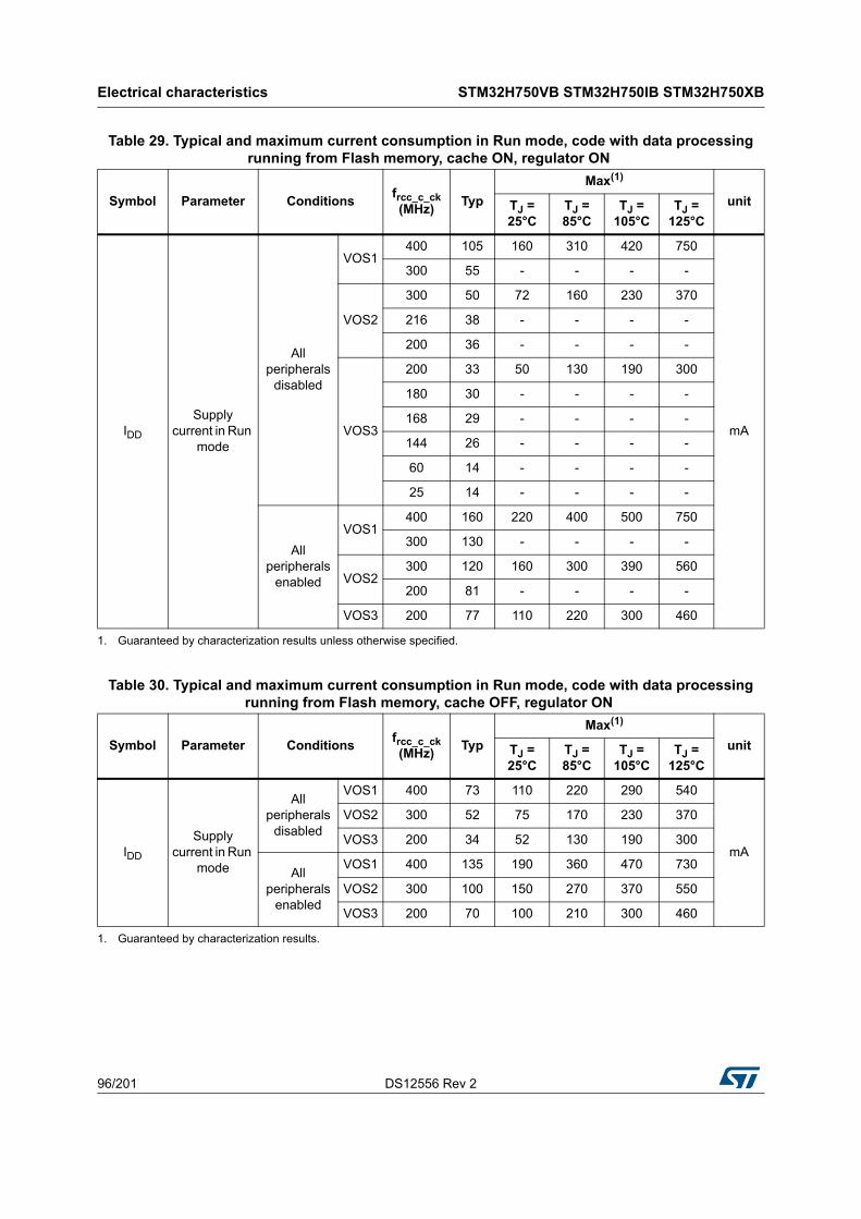
Electrical characteristics STM32H750VB STM32H750IB STM32H750XB
96/201 DS12556 Rev 2
Table 29. Typical and maximum current consumption in Run mode, code with data processingrunning from Flash memory, cache ON, regulator ON
Symbol Parameter Conditionsfrcc_c_ck (MHz)
Typ
Max(1)
unitTJ = 25°C
TJ = 85°C
TJ = 105°C
TJ = 125°C
IDD
Supply current in Run
mode
All peripherals
disabled
VOS1400 105 160 310 420 750
mA
300 55 - - - -
VOS2
300 50 72 160 230 370
216 38 - - - -
200 36 - - - -
VOS3
200 33 50 130 190 300
180 30 - - - -
168 29 - - - -
144 26 - - - -
60 14 - - - -
25 14 - - - -
All peripherals
enabled
VOS1400 160 220 400 500 750
300 130 - - - -
VOS2300 120 160 300 390 560
200 81 - - - -
VOS3 200 77 110 220 300 460
1. Guaranteed by characterization results unless otherwise specified.
Table 30. Typical and maximum current consumption in Run mode, code with data processingrunning from Flash memory, cache OFF, regulator ON
Symbol Parameter Conditionsfrcc_c_ck (MHz)
Typ
Max(1)
unitTJ = 25°C
TJ = 85°C
TJ = 105°C
TJ = 125°C
IDD
Supply current in Run
mode
All peripherals
disabled
VOS1 400 73 110 220 290 540
mA
VOS2 300 52 75 170 230 370
VOS3 200 34 52 130 190 300
All peripherals
enabled
VOS1 400 135 190 360 470 730
VOS2 300 100 150 270 370 550
VOS3 200 70 100 210 300 460
1. Guaranteed by characterization results.
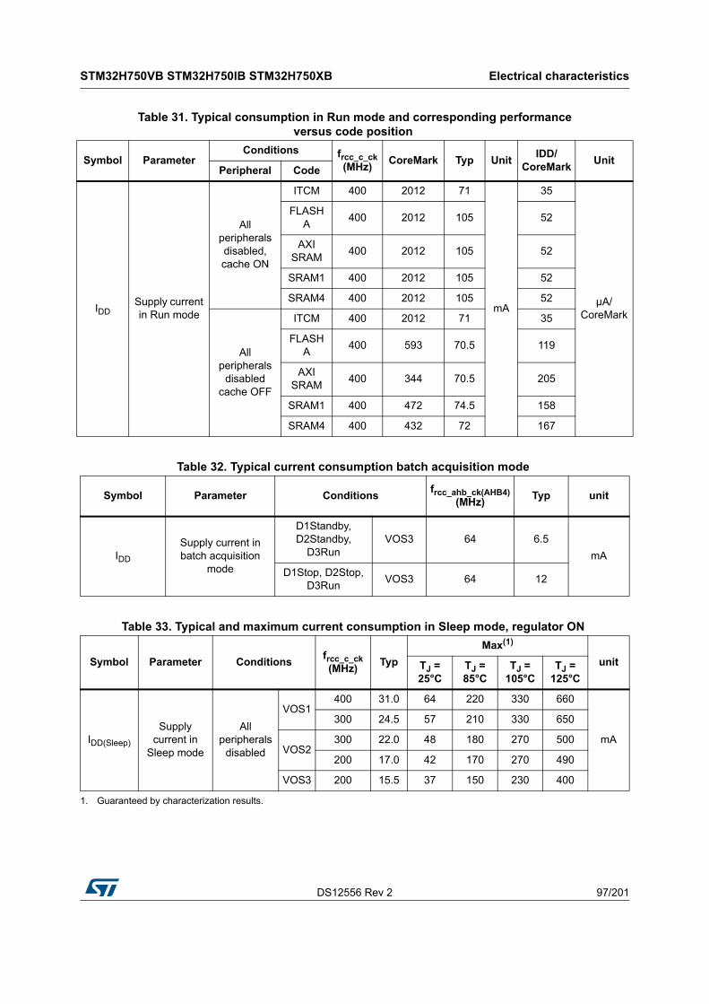
DS12556 Rev 2 97/201
STM32H750VB STM32H750IB STM32H750XB Electrical characteristics
189
Table 31. Typical consumption in Run mode and corresponding performance versus code position
Symbol ParameterConditions frcc_c_ck
(MHz)CoreMark Typ Unit
IDD/CoreMark
UnitPeripheral Code
IDDSupply current in Run mode
All peripherals disabled, cache ON
ITCM 400 2012 71
mA
35
µA/CoreMark
FLASH A
400 2012 105 52
AXI SRAM
400 2012 105 52
SRAM1 400 2012 105 52
SRAM4 400 2012 105 52
All peripherals
disabled cache OFF
ITCM 400 2012 71 35
FLASH A
400 593 70.5 119
AXI SRAM
400 344 70.5 205
SRAM1 400 472 74.5 158
SRAM4 400 432 72 167
Table 32. Typical current consumption batch acquisition mode
Symbol Parameter Conditionsfrcc_ahb_ck(AHB4)
(MHz)Typ unit
IDD
Supply current in batch acquisition
mode
D1Standby, D2Standby,
D3RunVOS3 64 6.5
mA
D1Stop, D2Stop, D3Run
VOS3 64 12
Table 33. Typical and maximum current consumption in Sleep mode, regulator ON
Symbol Parameter Conditionsfrcc_c_ck (MHz)
Typ
Max(1)
unitTJ = 25°C
TJ = 85°C
TJ = 105°C
TJ = 125°C
IDD(Sleep)
Supply current in
Sleep mode
All peripherals
disabled
VOS1400 31.0 64 220 330 660
mA
300 24.5 57 210 330 650
VOS2300 22.0 48 180 270 500
200 17.0 42 170 270 490
VOS3 200 15.5 37 150 230 400
1. Guaranteed by characterization results.
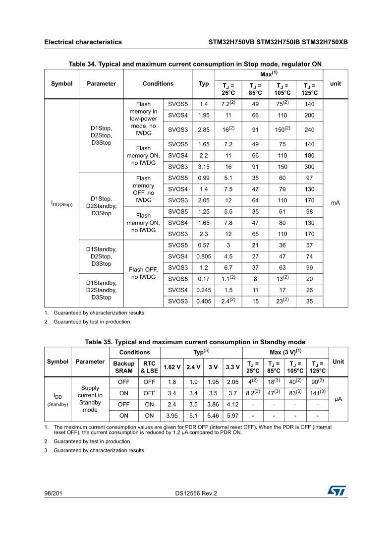
Electrical characteristics STM32H750VB STM32H750IB STM32H750XB
98/201 DS12556 Rev 2
Table 34. Typical and maximum current consumption in Stop mode, regulator ON
Symbol Parameter Conditions Typ
Max(1)
unitTJ = 25°C
TJ = 85°C
TJ = 105°C
TJ = 125°C
IDD(Stop)
D1Stop, D2Stop, D3Stop
Flash memory in low-power mode, no
IWDG
SVOS5 1.4 7.2(2) 49 75(2) 140
mA
SVOS4 1.95 11 66 110 200
SVOS3 2.85 16(2) 91 150(2) 240
Flash memory ON,
no IWDG
SVOS5 1.65 7.2 49 75 140
SVOS4 2.2 11 66 110 180
SVOS3 3.15 16 91 150 300
D1Stop, D2Standby,
D3Stop
Flash memory OFF, no IWDG
SVOS5 0.99 5.1 35 60 97
SVOS4 1.4 7.5 47 79 130
SVOS3 2.05 12 64 110 170
Flash memory ON,
no IWDG
SVOS5 1.25 5.5 35 61 98
SVOS4 1.65 7.8 47 80 130
SVOS3 2.3 12 65 110 170
D1Standby, D2Stop, D3Stop
Flash OFF, no IWDG
SVOS5 0.57 3 21 36 57
SVOS4 0.805 4.5 27 47 74
SVOS3 1.2 6.7 37 63 99
D1Standby, D2Standby,
D3Stop
SVOS5 0.17 1.1(2) 8 13(2) 20
SVOS4 0.245 1.5 11 17 26
SVOS3 0.405 2.4(2) 15 23(2) 35
1. Guaranteed by characterization results.
2. Guaranteed by test in production.
Table 35. Typical and maximum current consumption in Standby mode
Symbol Parameter
Conditions Typ(3) Max (3 V)(1)
UnitBackup SRAM
RTC & LSE
1.62 V 2.4 V 3 V 3.3 VTJ = 25°C
TJ = 85°C
TJ = 105°C
TJ = 125°C
IDD
(Standby)
Supply current in Standby
mode
OFF OFF 1.8 1.9 1.95 2.05 4(2) 18(3) 40(2) 90(3)
µAON OFF 3.4 3.4 3.5 3.7 8.2(3) 47(3) 83(3) 141(3)
OFF ON 2.4 3.5 3.86 4.12 - - - -
ON ON 3.95 5.1 5.46 5.97 - - - -
1. The maximum current consumption values are given for PDR OFF (internal reset OFF). When the PDR is OFF (internal reset OFF), the current consumption is reduced by 1.2 µA compared to PDR ON.
2. Guaranteed by test in production.
3. Guaranteed by characterization results.
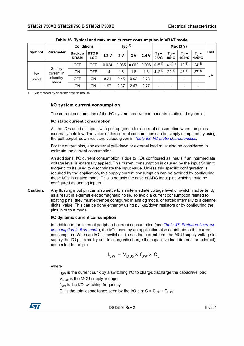
DS12556 Rev 2 99/201
STM32H750VB STM32H750IB STM32H750XB Electrical characteristics
189
I/O system current consumption
The current consumption of the I/O system has two components: static and dynamic.
I/O static current consumption
All the I/Os used as inputs with pull-up generate a current consumption when the pin is externally held low. The value of this current consumption can be simply computed by using the pull-up/pull-down resistors values given in Table 58: I/O static characteristics.
For the output pins, any external pull-down or external load must also be considered to estimate the current consumption.
An additional I/O current consumption is due to I/Os configured as inputs if an intermediate voltage level is externally applied. This current consumption is caused by the input Schmitt trigger circuits used to discriminate the input value. Unless this specific configuration is required by the application, this supply current consumption can be avoided by configuring these I/Os in analog mode. This is notably the case of ADC input pins which should be configured as analog inputs.
Caution: Any floating input pin can also settle to an intermediate voltage level or switch inadvertently, as a result of external electromagnetic noise. To avoid a current consumption related to floating pins, they must either be configured in analog mode, or forced internally to a definite digital value. This can be done either by using pull-up/down resistors or by configuring the pins in output mode.
I/O dynamic current consumption
In addition to the internal peripheral current consumption (see Table 37: Peripheral current consumption in Run mode), the I/Os used by an application also contribute to the current consumption. When an I/O pin switches, it uses the current from the MCU supply voltage to supply the I/O pin circuitry and to charge/discharge the capacitive load (internal or external) connected to the pin:
ISW VDDx fSW CL××=
where
ISW is the current sunk by a switching I/O to charge/discharge the capacitive load
VDDx is the MCU supply voltage
fSW is the I/O switching frequency
CL is the total capacitance seen by the I/O pin: C = CINT+ CEXT
Table 36. Typical and maximum current consumption in VBAT mode
Symbol Parameter
Conditions Typ(1) Max (3 V)
UnitBackup SRAM
RTC & LSE
1.2 V 2 V 3 V 3.4 VTJ = 25°C
TJ = 85°C
TJ = 105°C
TJ = 125°C
IDD
(VBAT)
Supply current in standby mode
OFF OFF 0.024 0.035 0.062 0.096 0.5(1) 4.1(1) 10(1) 24(1)
µAON OFF 1.4 1.6 1.8 1.8 4.4(1) 22(1) 48(1) 87(1)
OFF ON 0.24 0.45 0.62 0.73 - - - -
ON ON 1.97 2.37 2.57 2.77 - - - -
1. Guaranteed by characterization results.
Electrical characteristics STM32H750VB STM32H750IB STM32H750XB
100/201 DS12556 Rev 2
The test pin is configured in push-pull output mode and is toggled by software at a fixed frequency.
On-chip peripheral current consumption
The MCU is placed under the following conditions:
• At startup, all I/O pins are in analog input configuration.
• All peripherals are disabled unless otherwise mentioned.
• The I/O compensation cell is enabled.
• frcc_c_ck is the CPU clock. fPCLK = frcc_c_ck/4, and fHCLK = frcc_c_ck/2.
The given value is calculated by measuring the difference of current consumption
– with all peripherals clocked off
– with only one peripheral clocked on
– frcc_c_ck = 400 MHz (Scale 1), frcc_c_ck = 300 MHz (Scale 2), frcc_c_ck = 200 MHz (Scale 3)
• The ambient operating temperature is 25 °C and VDD=3.3 V.
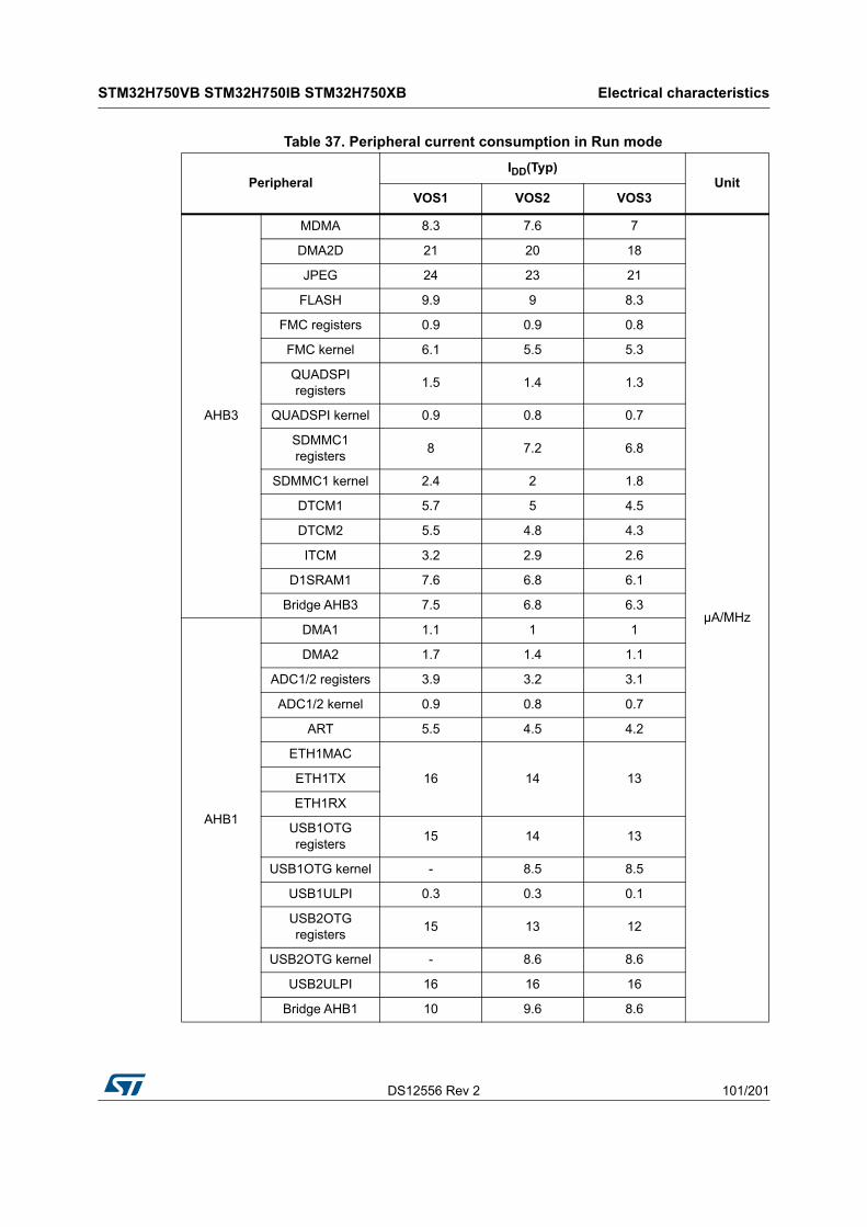
DS12556 Rev 2 101/201
STM32H750VB STM32H750IB STM32H750XB Electrical characteristics
189
Table 37. Peripheral current consumption in Run mode
PeripheralIDD(Typ)
UnitVOS1 VOS2 VOS3
AHB3
MDMA 8.3 7.6 7
µA/MHz
DMA2D 21 20 18
JPEG 24 23 21
FLASH 9.9 9 8.3
FMC registers 0.9 0.9 0.8
FMC kernel 6.1 5.5 5.3
QUADSPI registers
1.5 1.4 1.3
QUADSPI kernel 0.9 0.8 0.7
SDMMC1 registers
8 7.2 6.8
SDMMC1 kernel 2.4 2 1.8
DTCM1 5.7 5 4.5
DTCM2 5.5 4.8 4.3
ITCM 3.2 2.9 2.6
D1SRAM1 7.6 6.8 6.1
Bridge AHB3 7.5 6.8 6.3
AHB1
DMA1 1.1 1 1
DMA2 1.7 1.4 1.1
ADC1/2 registers 3.9 3.2 3.1
ADC1/2 kernel 0.9 0.8 0.7
ART 5.5 4.5 4.2
ETH1MAC
16 14 13ETH1TX
ETH1RX
USB1OTG registers
15 14 13
USB1OTG kernel - 8.5 8.5
USB1ULPI 0.3 0.3 0.1
USB2OTG registers
15 13 12
USB2OTG kernel - 8.6 8.6
USB2ULPI 16 16 16
Bridge AHB1 10 9.6 8.6

Electrical characteristics STM32H750VB STM32H750IB STM32H750XB
102/201 DS12556 Rev 2
AHB2
DCMI 1.7 1.7 1.7
µA/MHz
CRYPT 0.1 0.1 0.1
HASH 0.1 0.1 0.1
RNG registers 1.8 1.4 1.2
RNG kernel - 9.6 9.6
SDMMC2 registers
13 12 11
SDMMC2 kernel 2.7 2.5 2.4
D2SRAM1 3.3 3.1 2.8
D2SRAM2 2.9 2.7 2.5
D2SRAM3 1.9 1.8 1.7
Bridge AHB2 0.1 0.1 0.1
AHB4
GPIOA 1.1 1 0.9
GPIOB 1 0.9 0.9
GPIOC 1.4 1.3 1.3
GPIOD 1.1 1 0.9
GPIOE 1 0.9 0.8
GPIOF 0.9 0.8 0.8
GPIOG 0.9 0.7 0.7
GPIOH 1 0.9 0.9
GPIOI 0.9 0.9 0.8
GPIOJ 0.9 0.8 0.8
GPIOK 0.9 0.8 0.7
CRC 0.5 0.4 0.4
BDMA 6.2 5.8 5.5
ADC3 registers 1.8 1.7 1.7
ADC3 kernel 0.1 0.1 0.1
Backup SRAM 1.9 1.8 1.8
Bridge AHB4 0.1 0.1 0.1
APB3
LCD-TFT 12 11 10
µA/MHz
WWDG1 0.5 0.4 0.3
Bridge APB3 0.5 0.2 0.1
Table 37. Peripheral current consumption in Run mode (continued)
PeripheralIDD(Typ)
UnitVOS1 VOS2 VOS3

DS12556 Rev 2 103/201
STM32H750VB STM32H750IB STM32H750XB Electrical characteristics
189
APB1
TIM2 3.5 3.2 2.9
µA/MHz
TIM3 3.4 3.1 2.7
TIM4 2.7 2.5 1.9
TIM5 3.2 2.9 2.5
TIM6 1 0.8 0.7
TIM7 1 0.9 0.7
TIM12 1.7 1.5 1.2
TIM13 1.5 1.3 1
TIM14 1.4 1.3 0.9
LPTIM1 registers 0.7 0.6 0.5
LPTIM1 kernel 2.3 2.1 1.9
WWDG2 0.6 0.4 0.4
SPI2 registers 1.8 1.5 1.2
SPI2 kernel 0.6 0.5 0.5
SPI3 registers 1.5 1.3 1.1
SPI3 kernel 0.6 0.5 0.5
SPDIFRX registers
0.6 0.5 0.3
SPDIFRX kernel 2.9 2.4 2.4
USART2 registers 1.4 1.3 1
USART2 kernel 4.7 4.1 4
USART3 registers 1.4 1.3 1
USART3 kernel 4.2 3.8 3.5
UART4 registers 1.5 1.1 1
UART4 kernel 3.7 3.6 3.2
Table 37. Peripheral current consumption in Run mode (continued)
PeripheralIDD(Typ)
UnitVOS1 VOS2 VOS3
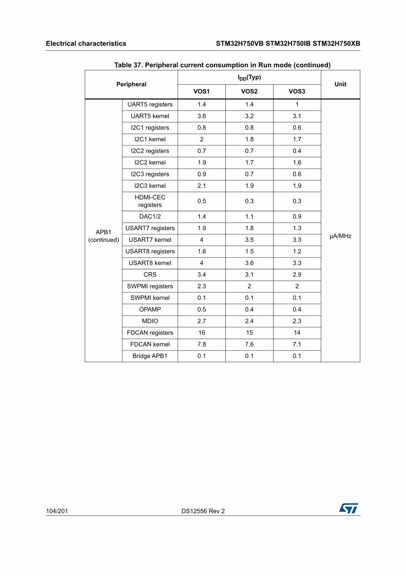
Electrical characteristics STM32H750VB STM32H750IB STM32H750XB
104/201 DS12556 Rev 2
APB1 (continued)
UART5 registers 1.4 1.4 1
µA/MHz
UART5 kernel 3.6 3.2 3.1
I2C1 registers 0.8 0.8 0.6
I2C1 kernel 2 1.8 1.7
I2C2 registers 0.7 0.7 0.4
I2C2 kernel 1.9 1.7 1.6
I2C3 registers 0.9 0.7 0.6
I2C3 kernel 2.1 1.9 1.9
HDMI-CEC registers
0.5 0.3 0.3
DAC1/2 1.4 1.1 0.9
USART7 registers 1.9 1.8 1.3
USART7 kernel 4 3.5 3.3
USART8 registers 1.6 1.5 1.2
USART8 kernel 4 3.6 3.3
CRS 3.4 3.1 2.9
SWPMI registers 2.3 2 2
SWPMI kernel 0.1 0.1 0.1
OPAMP 0.5 0.4 0.4
MDIO 2.7 2.4 2.3
FDCAN registers 16 15 14
FDCAN kernel 7.8 7.6 7.1
Bridge APB1 0.1 0.1 0.1
Table 37. Peripheral current consumption in Run mode (continued)
PeripheralIDD(Typ)
UnitVOS1 VOS2 VOS3
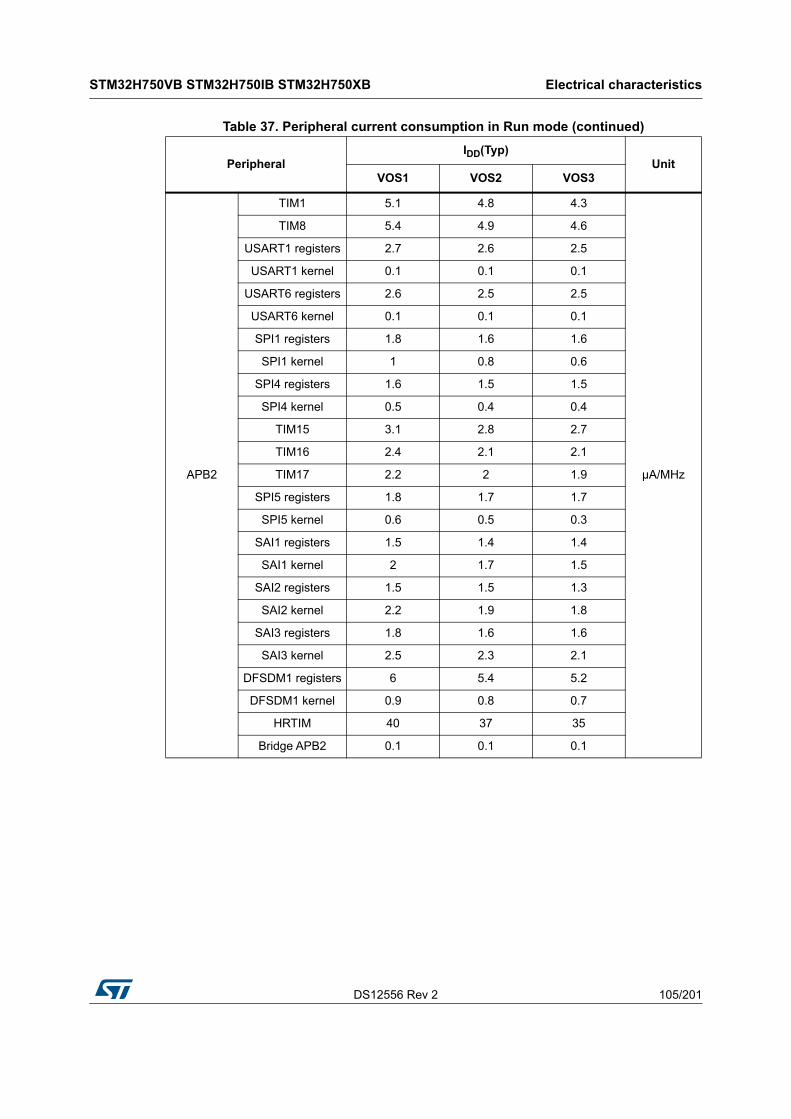
DS12556 Rev 2 105/201
STM32H750VB STM32H750IB STM32H750XB Electrical characteristics
189
APB2
TIM1 5.1 4.8 4.3
µA/MHz
TIM8 5.4 4.9 4.6
USART1 registers 2.7 2.6 2.5
USART1 kernel 0.1 0.1 0.1
USART6 registers 2.6 2.5 2.5
USART6 kernel 0.1 0.1 0.1
SPI1 registers 1.8 1.6 1.6
SPI1 kernel 1 0.8 0.6
SPI4 registers 1.6 1.5 1.5
SPI4 kernel 0.5 0.4 0.4
TIM15 3.1 2.8 2.7
TIM16 2.4 2.1 2.1
TIM17 2.2 2 1.9
SPI5 registers 1.8 1.7 1.7
SPI5 kernel 0.6 0.5 0.3
SAI1 registers 1.5 1.4 1.4
SAI1 kernel 2 1.7 1.5
SAI2 registers 1.5 1.5 1.3
SAI2 kernel 2.2 1.9 1.8
SAI3 registers 1.8 1.6 1.6
SAI3 kernel 2.5 2.3 2.1
DFSDM1 registers 6 5.4 5.2
DFSDM1 kernel 0.9 0.8 0.7
HRTIM 40 37 35
Bridge APB2 0.1 0.1 0.1
Table 37. Peripheral current consumption in Run mode (continued)
PeripheralIDD(Typ)
UnitVOS1 VOS2 VOS3
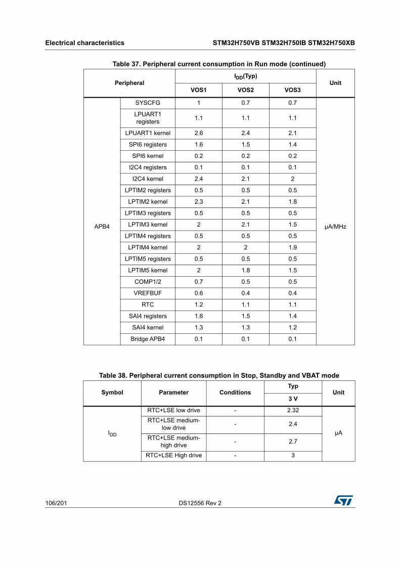
Electrical characteristics STM32H750VB STM32H750IB STM32H750XB
106/201 DS12556 Rev 2
APB4
SYSCFG 1 0.7 0.7
µA/MHz
LPUART1 registers
1.1 1.1 1.1
LPUART1 kernel 2.6 2.4 2.1
SPI6 registers 1.6 1.5 1.4
SPI6 kernel 0.2 0.2 0.2
I2C4 registers 0.1 0.1 0.1
I2C4 kernel 2.4 2.1 2
LPTIM2 registers 0.5 0.5 0.5
LPTIM2 kernel 2.3 2.1 1.8
LPTIM3 registers 0.5 0.5 0.5
LPTIM3 kernel 2 2.1 1.5
LPTIM4 registers 0.5 0.5 0.5
LPTIM4 kernel 2 2 1.9
LPTIM5 registers 0.5 0.5 0.5
LPTIM5 kernel 2 1.8 1.5
COMP1/2 0.7 0.5 0.5
VREFBUF 0.6 0.4 0.4
RTC 1.2 1.1 1.1
SAI4 registers 1.6 1.5 1.4
SAI4 kernel 1.3 1.3 1.2
Bridge APB4 0.1 0.1 0.1
Table 38. Peripheral current consumption in Stop, Standby and VBAT mode
Symbol Parameter ConditionsTyp
Unit3 V
IDD
RTC+LSE low drive - 2.32
µA
RTC+LSE medium-low drive
- 2.4
RTC+LSE medium-high drive
- 2.7
RTC+LSE High drive - 3
Table 37. Peripheral current consumption in Run mode (continued)
PeripheralIDD(Typ)
UnitVOS1 VOS2 VOS3

DS12556 Rev 2 107/201
STM32H750VB STM32H750IB STM32H750XB Electrical characteristics
189
6.3.7 Wakeup time from low-power modes
The wakeup times given in Table 39 are measured starting from the wakeup event trigger up to the first instruction executed by the CPU:
• For Stop or Sleep modes: the wakeup event is WFE.
• WKUP (PC1) pin is used to wakeup from Standby, Stop and Sleep modes.
All timings are derived from tests performed under ambient temperature and VDD=3.3 V.
Table 39. Low-power mode wakeup timings
Symbol Parameter Conditions Typ(1) Max(1) Unit
tWUSLEEP(2) Wakeup from Sleep - 9 10
CPU clock cycles
tWUSTOP(2) Wakeup from Stop
VOS3, HSI, Flash memory in normal mode 4.4 5.6
µs
VOS3, HSI, Flash memory in low-power mode
12 15
VOS4, HSI, Flash memory in normal mode 15 20
VOS4, HSI, Flash memory in low-power mode
23 28
VOS5, HSI, Flash memory in normal mode 30 71
VOS5, HSI, Flash memory in low-power mode
38 47
VOS3, CSI, Flash memory in normal mode 27 37
VOS3, CSI, Flash memory in low power mode
36 50
VOS4, CSI, Flash memory in normal mode 38 48
VOS4, CSI, Flash memory in low-power mode
47 61
VOS5, CSI, Flash memory in normal mode 52 64
VOS5, CSI, Flash memory in low-power mode
62 77
tWUSTOP2(2) Wakeup from Stop,
clock kept running
VOS3, HSI, Flash memory in normal mode 2.6 3.4
VOS3, CSI, Flash memory in normal mode 26 36
tWUSTDBY(2) Wakeup from Standby
mode- 390 500
1. Guaranteed by characterization results.
2. The wakeup times are measured from the wakeup event to the point in which the application code reads the first instruction.
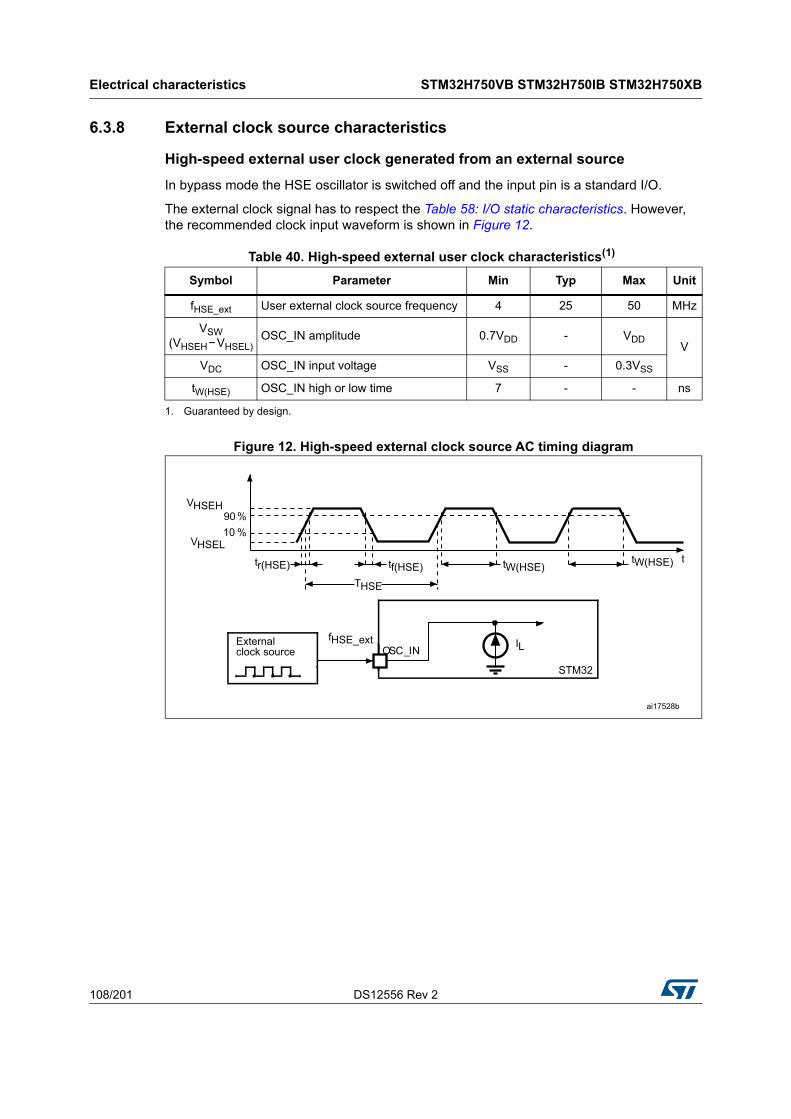
Electrical characteristics STM32H750VB STM32H750IB STM32H750XB
108/201 DS12556 Rev 2
6.3.8 External clock source characteristics
High-speed external user clock generated from an external source
In bypass mode the HSE oscillator is switched off and the input pin is a standard I/O.
The external clock signal has to respect the Table 58: I/O static characteristics. However, the recommended clock input waveform is shown in Figure 12.
Figure 12. High-speed external clock source AC timing diagram
Table 40. High-speed external user clock characteristics(1)
1. Guaranteed by design.
Symbol Parameter Min Typ Max Unit
fHSE_ext User external clock source frequency 4 25 50 MHz
VSW (VHSEH−VHSEL)
OSC_IN amplitude 0.7VDD - VDDV
VDC OSC_IN input voltage VSS - 0.3VSS
tW(HSE) OSC_IN high or low time 7 - - ns
ai17528b
OSC_INExternal
STM32
clock source
VHSEH
tf(HSE) tW(HSE)
IL
90 %10 %
THSE
ttr(HSE) tW(HSE)
fHSE_ext
VHSEL
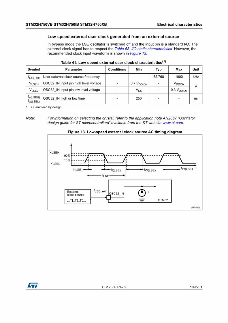
DS12556 Rev 2 109/201
STM32H750VB STM32H750IB STM32H750XB Electrical characteristics
189
Low-speed external user clock generated from an external source
In bypass mode the LSE oscillator is switched off and the input pin is a standard I/O. The external clock signal has to respect the Table 58: I/O static characteristics. However, the recommended clock input waveform is shown in Figure 13.
Note: For information on selecting the crystal, refer to the application note AN2867 “Oscillator design guide for ST microcontrollers” available from the ST website www.st.com.
Figure 13. Low-speed external clock source AC timing diagram
Table 41. Low-speed external user clock characteristics(1)
Symbol Parameter Conditions Min Typ Max Unit
fLSE_ext User external clock source frequency - - 32.768 1000 kHz
VLSEH OSC32_IN input pin high level voltage - 0.7 VDDIOx - VDDIOxV
VLSEL OSC32_IN input pin low level voltage - VSS - 0.3 VDDIOx
tw(LSEH)tw(LSEL)
OSC32_IN high or low time - 250 - - ns
1. Guaranteed by design.
ai17529b
OSC32_INExternal
STM32
clock source
VLSEH
tf(LSE) tW(LSE)
IL
90%10%
TLSE
ttr(LSE) tW(LSE)
fLSE_ext
VLSEL
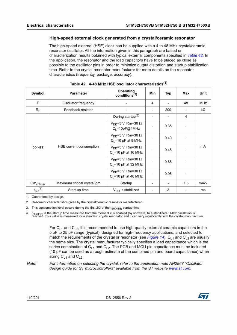
Electrical characteristics STM32H750VB STM32H750IB STM32H750XB
110/201 DS12556 Rev 2
High-speed external clock generated from a crystal/ceramic resonator
The high-speed external (HSE) clock can be supplied with a 4 to 48 MHz crystal/ceramic resonator oscillator. All the information given in this paragraph are based on characterization results obtained with typical external components specified in Table 42. In the application, the resonator and the load capacitors have to be placed as close as possible to the oscillator pins in order to minimize output distortion and startup stabilization time. Refer to the crystal resonator manufacturer for more details on the resonator characteristics (frequency, package, accuracy).
For CL1 and CL2, it is recommended to use high-quality external ceramic capacitors in the 5 pF to 25 pF range (typical), designed for high-frequency applications, and selected to match the requirements of the crystal or resonator (see Figure 14). CL1 and CL2 are usually the same size. The crystal manufacturer typically specifies a load capacitance which is the series combination of CL1 and CL2. The PCB and MCU pin capacitance must be included (10 pF can be used as a rough estimate of the combined pin and board capacitance) when sizing CL1 and CL2.
Note: For information on selecting the crystal, refer to the application note AN2867 “Oscillator design guide for ST microcontrollers” available from the ST website www.st.com.
Table 42. 4-48 MHz HSE oscillator characteristics(1)
Symbol ParameterOperating
conditions(2) Min Typ Max Unit
F Oscillator frequency - 4 - 48 MHz
RF Feedback resistor - - 200 - kΩ
IDD(HSE) HSE current consumption
During startup(3) - - 4
mA
VDD=3 V, Rm=30 Ω
CL=10pF@4MHz- 0.35 -
VDD=3 V, Rm=30 Ω
CL=10 pF at 8 MHz- 0.40 -
VDD=3 V, Rm=30 Ω
CL=10 pF at 16 MHz- 0.45 -
VDD=3 V, Rm=30 Ω
CL=10 pF at 32 MHz- 0.65 -
VDD=3 V, Rm=30 Ω
CL=10 pF at 48 MHz- 0.95 -
Gmcritmax Maximum critical crystal gm Startup - - 1.5 mA/V
tSU(4) Start-up time VDD is stabilized - 2 - ms
1. Guaranteed by design.
2. Resonator characteristics given by the crystal/ceramic resonator manufacturer.
3. This consumption level occurs during the first 2/3 of the tSU(HSE) startup time.
4. tSU(HSE) is the startup time measured from the moment it is enabled (by software) to a stabilized 8 MHz oscillation is reached. This value is measured for a standard crystal resonator and it can vary significantly with the crystal manufacturer.

DS12556 Rev 2 111/201
STM32H750VB STM32H750IB STM32H750XB Electrical characteristics
189
Figure 14. Typical application with an 8 MHz crystal
1. REXT value depends on the crystal characteristics.
Low-speed external clock generated from a crystal/ceramic resonator
The low-speed external (LSE) clock can be supplied with a 32.768 kHz crystal/ceramic resonator oscillator. All the information given in this paragraph are based on characterization results obtained with typical external components specified in Table 43. In the application, the resonator and the load capacitors have to be placed as close as possible to the oscillator pins in order to minimize output distortion and startup stabilization time. Refer to the crystal resonator manufacturer for more details on the resonator characteristics (frequency, package, accuracy).
ai17530b
OSC_OUT
OSC_IN fHSECL1
RF
STM32
8 MHzresonator
Resonator withintegrated capacitors
Bias controlled
gain
REXT(1) CL2
Table 43. Low-speed external user clock characteristics(1)
Symbol Parameter Operating conditions(2) Min Typ Max Unit
F Oscillator frequency - - 32.768 - kHz
IDDLSE current consumption
LSEDRV[1:0] = 00, Low drive capability
- 290 -
nA
LSEDRV[1:0] = 01, Medium Low drive capability
- 390 -
LSEDRV[1:0] = 10, Medium high drive capability
- 550 -
LSEDRV[1:0] = 11, High drive capability
- 900 -
GmcritmaxMaximum critical crystal
gm
LSEDRV[1:0] = 00, Low drive capability
- - 0.5
µA/V
LSEDRV[1:0] = 01, Medium Low drive capability
- - 0.75
LSEDRV[1:0] = 10, Medium high drive capability
- - 1.7
LSEDRV[1:0] = 11, High drive capability
- - 2.7
tSU(3) Startup time VDD is stabilized - 2 - s
1. Guaranteed by design.
2. Refer to the note and caution paragraphs below the table, and to the application note AN2867 “Oscillator design guide for ST microcontrollers.
3. tSU is the startup time measured from the moment it is enabled (by software) to a stabilized 32.768k Hz oscillation is reached. This value is measured for a standard crystal resonator and it can vary significantly with the crystal manufacturer.
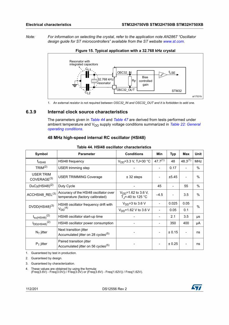
Electrical characteristics STM32H750VB STM32H750IB STM32H750XB
112/201 DS12556 Rev 2
Note: For information on selecting the crystal, refer to the application note AN2867 “Oscillator design guide for ST microcontrollers” available from the ST website www.st.com.
Figure 15. Typical application with a 32.768 kHz crystal
1. An external resistor is not required between OSC32_IN and OSC32_OUT and it is forbidden to add one.
6.3.9 Internal clock source characteristics
The parameters given in Table 44 and Table 47 are derived from tests performed under ambient temperature and VDD supply voltage conditions summarized in Table 22: General operating conditions.
48 MHz high-speed internal RC oscillator (HSI48)
ai17531b
OSC32_OUT
OSC32_IN fLSECL1
RF
STM32
32.768 kHzresonator
Resonator withintegrated capacitors
Bias controlled
gain
CL2
Table 44. HSI48 oscillator characteristics
Symbol Parameter Conditions Min Typ Max Unit
fHSI48 HSI48 frequency VDD=3.3 V, TJ=30 °C 47.7(1) 48 48.3(1) MHz
TRIM(2) USER trimming step - - 0.17 - %
USER TRIM
COVERAGE(3) USER TRIMMING Coverage ± 32 steps - ±5.45 - %
DuCy(HSI48)(2) Duty Cycle - 45 - 55 %
ACCHSI48_REL(3) Accuracy of the HSI48 oscillator over temperature (factory calibrated)
VDD=1.62 to 3.6 V, TJ=-40 to 125 °C
–4.5 - 3.5 %
DVDD(HSI48)(3) HSI48 oscillator frequency drift with VDD
(4)
VDD=3 to 3.6 V - 0.025 0.05%
VDD=1.62 V to 3.6 V - 0.05 0.1
tsu(HSI48)(2) HSI48 oscillator start-up time - - 2.1 3.5 µs
IDD(HSI48)(2) HSI48 oscillator power consumption - - 350 400 µA
NT jitterNext transition jitter
Accumulated jitter on 28 cycles(5) - - ± 0.15 - ns
PT jitterPaired transition jitter
Accumulated jitter on 56 cycles(5) - - ± 0.25 - ns
1. Guaranteed by test in production.
2. Guaranteed by design.
3. Guaranteed by characterization.
4. These values are obtained by using the formula: (Freq(3.6V) - Freq(3.0V)) / Freq(3.0V) or (Freq(3.6V) - Freq(1.62V)) / Freq(1.62V).
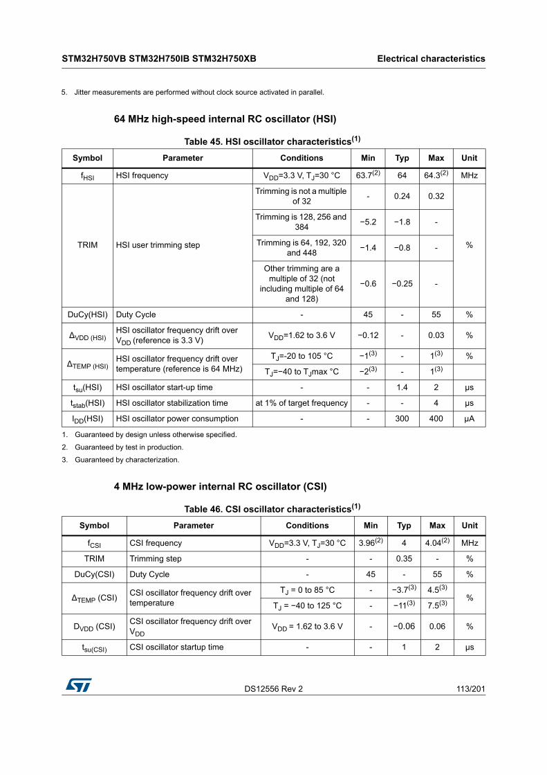
DS12556 Rev 2 113/201
STM32H750VB STM32H750IB STM32H750XB Electrical characteristics
189
64 MHz high-speed internal RC oscillator (HSI)
4 MHz low-power internal RC oscillator (CSI)
5. Jitter measurements are performed without clock source activated in parallel.
Table 45. HSI oscillator characteristics(1)
Symbol Parameter Conditions Min Typ Max Unit
fHSI HSI frequency VDD=3.3 V, TJ=30 °C 63.7(2) 64 64.3(2) MHz
TRIM HSI user trimming step
Trimming is not a multiple of 32
- 0.24 0.32
%
Trimming is 128, 256 and 384
−5.2 −1.8 -
Trimming is 64, 192, 320 and 448
−1.4 −0.8 -
Other trimming are a multiple of 32 (not
including multiple of 64 and 128)
−0.6 −0.25 -
DuCy(HSI) Duty Cycle - 45 - 55 %
ΔVDD (HSI)HSI oscillator frequency drift over VDD (reference is 3.3 V)
VDD=1.62 to 3.6 V −0.12 - 0.03 %
ΔTEMP (HSI)HSI oscillator frequency drift over temperature (reference is 64 MHz)
TJ=-20 to 105 °C −1(3) - 1(3) %
TJ=−40 to TJmax °C −2(3) - 1(3)
tsu(HSI) HSI oscillator start-up time - - 1.4 2 µs
tstab(HSI) HSI oscillator stabilization time at 1% of target frequency - - 4 µs
IDD(HSI) HSI oscillator power consumption - - 300 400 µA
1. Guaranteed by design unless otherwise specified.
2. Guaranteed by test in production.
3. Guaranteed by characterization.
Table 46. CSI oscillator characteristics(1)
Symbol Parameter Conditions Min Typ Max Unit
fCSI CSI frequency VDD=3.3 V, TJ=30 °C 3.96(2) 4 4.04(2) MHz
TRIM Trimming step - - 0.35 - %
DuCy(CSI) Duty Cycle - 45 - 55 %
∆TEMP (CSI)CSI oscillator frequency drift over temperature
TJ = 0 to 85 °C - −3.7(3) 4.5(3)
%TJ = −40 to 125 °C - −11(3) 7.5(3)
DVDD (CSI)CSI oscillator frequency drift over VDD
VDD = 1.62 to 3.6 V - −0.06 0.06 %
tsu(CSI) CSI oscillator startup time - - 1 2 µs

Electrical characteristics STM32H750VB STM32H750IB STM32H750XB
114/201 DS12556 Rev 2
Low-speed internal (LSI) RC oscillator
6.3.10 PLL characteristics
The parameters given in Table 48 are derived from tests performed under temperature and VDD supply voltage conditions summarized in Table 22: General operating conditions.
tstab(CSI)CSI oscillator stabilization time (to reach ±3% of fCSI)
- - - 4 cycle
IDD(CSI) CSI oscillator power consumption - - 23 30 µA
1. Guaranteed by design.
2. Guaranteed by test in production.
3. Guaranteed by characterization.
Table 46. CSI oscillator characteristics(1) (continued)
Symbol Parameter Conditions Min Typ Max Unit
Table 47. LSI oscillator characteristics
Symbol Parameter Conditions Min Typ Max Unit
fLSI(1)
1. Guaranteed by characterization results.
LSI frequency
VDD = 3.3 V, TJ = 25 °C (after calibration)
31.4 32 32.6
kHz
TJ = –40 to 105 °C, VDD = 1.62 to 3.6 V
29.76 - 33.60
tsu(LSI)(2)
2. Guaranteed by design.
LSI oscillator startup time - - 80 130
µststab(LSI)
(2) LSI oscillator stabilization time (5% of final value)
- - 120 170
IDD(LSI)(2) LSI oscillator power
consumption- - 130 280 nA
Table 48. PLL characteristics (wide VCO frequency range)(1)
Symbol Parameter Conditions Min Typ Max Unit
fPLL_IN
PLL input clock - 2 - 16 MHz
PLL input clock duty cycle - 10 - 90 %
fPLL_P_OUT PLL multiplier output clock P
Voltage scaling range 1 1.5 - 400(2)
MHz
Voltage scaling range 2 1.5 - 300
Voltage scaling range 3 1.5 - 200
fPLL_Q_OUT PLL multiplier output clock Q/R
Voltage scaling range 1 1.5 - 400(2)
Voltage scaling range 2 1.5 - 300
Voltage scaling range 3 1.5 - 200
fVCO_OUT PLL VCO output - 192 - 836
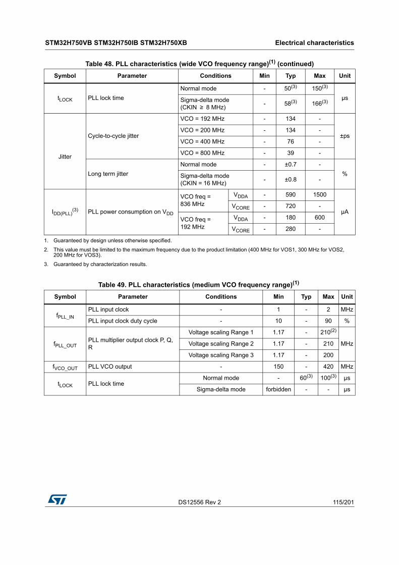
DS12556 Rev 2 115/201
STM32H750VB STM32H750IB STM32H750XB Electrical characteristics
189
tLOCK PLL lock time
Normal mode - 50(3) 150(3)
µsSigma-delta mode (CKIN ≥ 8 MHz)
- 58(3) 166(3)
Jitter
Cycle-to-cycle jitter
VCO = 192 MHz - 134 -
±psVCO = 200 MHz - 134 -
VCO = 400 MHz - 76 -
VCO = 800 MHz - 39 -
Long term jitter
Normal mode - ±0.7 -
%Sigma-delta mode (CKIN = 16 MHz)
- ±0.8 -
IDD(PLL)(3) PLL power consumption on VDD
VCO freq = 836 MHz
VDDA - 590 1500
µAVCORE - 720 -
VCO freq = 192 MHz
VDDA - 180 600
VCORE - 280 -
1. Guaranteed by design unless otherwise specified.
2. This value must be limited to the maximum frequency due to the product limitation (400 MHz for VOS1, 300 MHz for VOS2, 200 MHz for VOS3).
3. Guaranteed by characterization results.
Table 48. PLL characteristics (wide VCO frequency range)(1) (continued)
Symbol Parameter Conditions Min Typ Max Unit
Table 49. PLL characteristics (medium VCO frequency range)(1)
Symbol Parameter Conditions Min Typ Max Unit
fPLL_IN
PLL input clock - 1 - 2 MHz
PLL input clock duty cycle - 10 - 90 %
fPLL_OUTPLL multiplier output clock P, Q, R
Voltage scaling Range 1 1.17 - 210(2)
MHzVoltage scaling Range 2 1.17 - 210
Voltage scaling Range 3 1.17 - 200
fVCO_OUT PLL VCO output - 150 - 420 MHz
tLOCK PLL lock timeNormal mode - 60(3) 100(3) µs
Sigma-delta mode forbidden - - µs
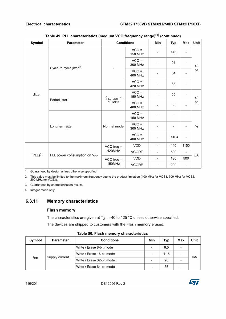
Electrical characteristics STM32H750VB STM32H750IB STM32H750XB
116/201 DS12556 Rev 2
6.3.11 Memory characteristics
Flash memory
The characteristics are given at TJ = –40 to 125 °C unless otherwise specified.
The devices are shipped to customers with the Flash memory erased.
Jitter
Cycle-to-cycle jitter(4) -
VCO = 150 MHz
- 145 -
+/-ps
VCO = 300 MHz
- 91 -
VCO = 400 MHz
- 64 -
VCO = 420 MHz
- 63 -
Period jitterfPLL_OUT =
50 MHz
VCO = 150 MHz
- 55 -+/-psVCO =
400 MHz- 30 -
Long term jitter Normal mode
VCO = 150 MHz
- - -
%VCO =
300 MHz- - -
VCO = 400 MHz
- +/-0.3 -
I(PLL)(3) PLL power consumption on VDD
VCO freq = 420MHz
VDD - 440 1150
µAVCORE - 530 -
VCO freq = 150MHz
VDD - 180 500
VCORE - 200 -
1. Guaranteed by design unless otherwise specified.
2. This value must be limited to the maximum frequency due to the product limitation (400 MHz for VOS1, 300 MHz for VOS2, 200 MHz for VOS3).
3. Guaranteed by characterization results.
4. Integer mode only.
Table 49. PLL characteristics (medium VCO frequency range)(1) (continued)
Symbol Parameter Conditions Min Typ Max Unit
Table 50. Flash memory characteristics
Symbol Parameter Conditions Min Typ Max Unit
IDD Supply current
Write / Erase 8-bit mode - 6.5 -
mAWrite / Erase 16-bit mode - 11.5 -
Write / Erase 32-bit mode - 20 -
Write / Erase 64-bit mode - 35 -
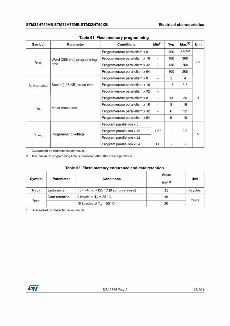
DS12556 Rev 2 117/201
STM32H750VB STM32H750IB STM32H750XB Electrical characteristics
189
Table 51. Flash memory programming
Symbol Parameter Conditions Min(1) Typ Max(1) Unit
tprogWord (266 bits) programming time
Program/erase parallelism x 8 - 290 580(2)
µsProgram/erase parallelism x 16 - 180 360
Program/erase parallelism x 32 - 130 260
Program/erase parallelism x 64 - 100 200
tERASE128KB Sector (128 KB) erase time
Program/erase parallelism x 8 - 2 4
s
Program/erase parallelism x 16 - 1.8 3.6
Program/erase parallelism x 32 -
tME Mass erase time
Program/erase parallelism x 8 - 13 26
Program/erase parallelism x 16 - 8 16
Program/erase parallelism x 32 - 6 12
Program/erase parallelism x 64 - 5 10
Vprog Programming voltage
Program parallelism x 8
1.62 - 3.6V
Program parallelism x 16
Program parallelism x 32
Program parallelism x 64 1.8 - 3.6
1. Guaranteed by characterization results.
2. The maximum programming time is measured after 10K erase operations.
Table 52. Flash memory endurance and data retention
Symbol Parameter ConditionsValue
UnitMin(1)
NEND Endurance TJ = –40 to +125 °C (6 suffix versions) 10 kcycles
tRET
Data retention 1 kcycle at TA = 85 °C 30Years
10 kcycles at TA = 55 °C 20
1. Guaranteed by characterization results.
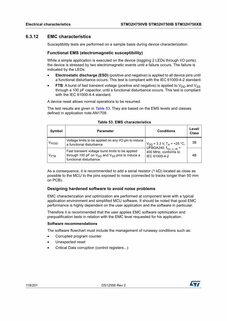
Electrical characteristics STM32H750VB STM32H750IB STM32H750XB
118/201 DS12556 Rev 2
6.3.12 EMC characteristics
Susceptibility tests are performed on a sample basis during device characterization.
Functional EMS (electromagnetic susceptibility)
While a simple application is executed on the device (toggling 2 LEDs through I/O ports). the device is stressed by two electromagnetic events until a failure occurs. The failure is indicated by the LEDs:
• Electrostatic discharge (ESD) (positive and negative) is applied to all device pins until a functional disturbance occurs. This test is compliant with the IEC 61000-4-2 standard.
• FTB: A burst of fast transient voltage (positive and negative) is applied to VDD and VSS through a 100 pF capacitor, until a functional disturbance occurs. This test is compliant with the IEC 61000-4-4 standard.
A device reset allows normal operations to be resumed.
The test results are given in Table 53. They are based on the EMS levels and classes defined in application note AN1709.
As a consequence, it is recommended to add a serial resistor (1 kΏ) located as close as possible to the MCU to the pins exposed to noise (connected to tracks longer than 50 mm on PCB).
Designing hardened software to avoid noise problems
EMC characterization and optimization are performed at component level with a typical application environment and simplified MCU software. It should be noted that good EMC performance is highly dependent on the user application and the software in particular.
Therefore it is recommended that the user applies EMC software optimization and prequalification tests in relation with the EMC level requested for his application.
Software recommendations
The software flowchart must include the management of runaway conditions such as:
• Corrupted program counter
• Unexpected reset
• Critical Data corruption (control registers...)
Table 53. EMS characteristics
Symbol Parameter ConditionsLevel/Class
VFESDVoltage limits to be applied on any I/O pin to induce a functional disturbance VDD = 3.3 V, TA = +25 °C,
UFBGA240, frcc_c_ck = 400 MHz, conforms to IEC 61000-4-2
3B
VFTB
Fast transient voltage burst limits to be applied through 100 pF on VDD and VSS pins to induce a functional disturbance
4B

DS12556 Rev 2 119/201
STM32H750VB STM32H750IB STM32H750XB Electrical characteristics
189
Prequalification trials
Most of the common failures (unexpected reset and program counter corruption) can be reproduced by manually forcing a low state on the NRST pin or the Oscillator pins for 1 second.
To complete these trials, ESD stress can be applied directly on the device, over the range of specification values. When unexpected behavior is detected, the software can be hardened to prevent unrecoverable errors occurring (see application note AN1015).
Electromagnetic Interference (EMI)
The electromagnetic field emitted by the device are monitored while a simple application, executing EEMBC code, is running. This emission test is compliant with SAE IEC61967-2 standard which specifies the test board and the pin loading.
6.3.13 Absolute maximum ratings (electrical sensitivity)
Based on three different tests (ESD, LU) using specific measurement methods, the device is stressed in order to determine its performance in terms of electrical sensitivity.
Electrostatic discharge (ESD)
Electrostatic discharges (a positive then a negative pulse) are applied to the pins of each sample according to each pin combination. This test conforms to the ANSI/ESDA/JEDEC JS-001 and ANSI/ESDA/JEDEC JS-002 standards.
Table 54. EMI characteristics
Symbol Parameter ConditionsMonitored
frequency band
Max vs. [fHSE/fCPU] Unit
8/400 MHz
SEMI Peak levelVDD = 3.6 V, TA = 25 °C, UFBGA240 package, conforming to IEC61967-2
0.1 to 30 MHz 6
dBµV30 to 130 MHz 5
130 MHz to 1 GHz 13
1 GHz to 2 GHz 7
EMI Level 2.5 -
Table 55. ESD absolute maximum ratings
Symbol Ratings Conditions Packages ClassMaximum value(1) Unit
VESD(HBM)
Electrostatic discharge voltage (human body model)
TA = +25 °C conforming to ANSI/ESDA/JEDEC JS-001
All 1C 1000
V
VESD(CDM)
Electrostatic discharge voltage (charge device model)
TA = +25 °C conforming to ANSI/ESDA/JEDEC JS-002
All C1 250
1. Guaranteed by characterization results.
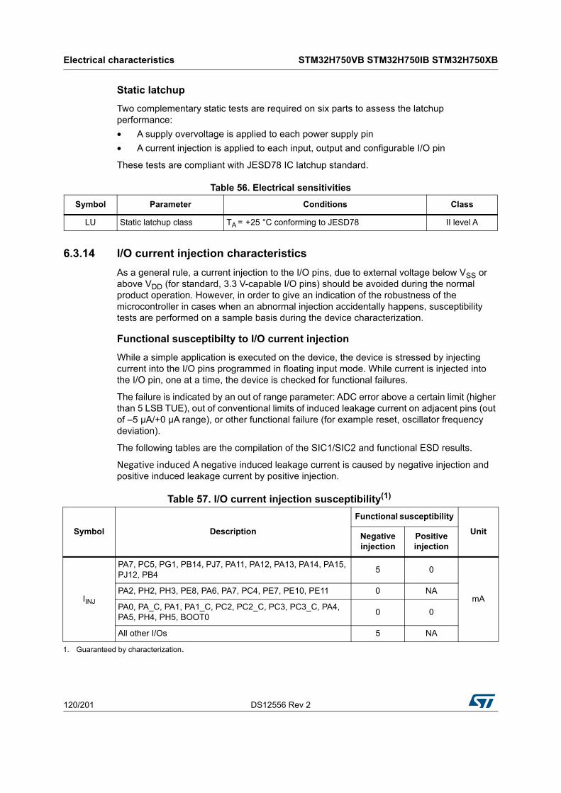
Electrical characteristics STM32H750VB STM32H750IB STM32H750XB
120/201 DS12556 Rev 2
Static latchup
Two complementary static tests are required on six parts to assess the latchup performance:
• A supply overvoltage is applied to each power supply pin
• A current injection is applied to each input, output and configurable I/O pin
These tests are compliant with JESD78 IC latchup standard.
6.3.14 I/O current injection characteristics
As a general rule, a current injection to the I/O pins, due to external voltage below VSS or above VDD (for standard, 3.3 V-capable I/O pins) should be avoided during the normal product operation. However, in order to give an indication of the robustness of the microcontroller in cases when an abnormal injection accidentally happens, susceptibility tests are performed on a sample basis during the device characterization.
Functional susceptibilty to I/O current injection
While a simple application is executed on the device, the device is stressed by injecting current into the I/O pins programmed in floating input mode. While current is injected into the I/O pin, one at a time, the device is checked for functional failures.
The failure is indicated by an out of range parameter: ADC error above a certain limit (higher than 5 LSB TUE), out of conventional limits of induced leakage current on adjacent pins (out of –5 µA/+0 µA range), or other functional failure (for example reset, oscillator frequency deviation).
The following tables are the compilation of the SIC1/SIC2 and functional ESD results.
Negative induced A negative induced leakage current is caused by negative injection and positive induced leakage current by positive injection.
Table 56. Electrical sensitivities
Symbol Parameter Conditions Class
LU Static latchup class TA = +25 °C conforming to JESD78 II level A
Table 57. I/O current injection susceptibility(1)
Symbol Description
Functional susceptibility
UnitNegative injection
Positive injection
IINJ
PA7, PC5, PG1, PB14, PJ7, PA11, PA12, PA13, PA14, PA15, PJ12, PB4
5 0
mAPA2, PH2, PH3, PE8, PA6, PA7, PC4, PE7, PE10, PE11 0 NA
PA0, PA_C, PA1, PA1_C, PC2, PC2_C, PC3, PC3_C, PA4, PA5, PH4, PH5, BOOT0
0 0
All other I/Os 5 NA
1. Guaranteed by characterization.
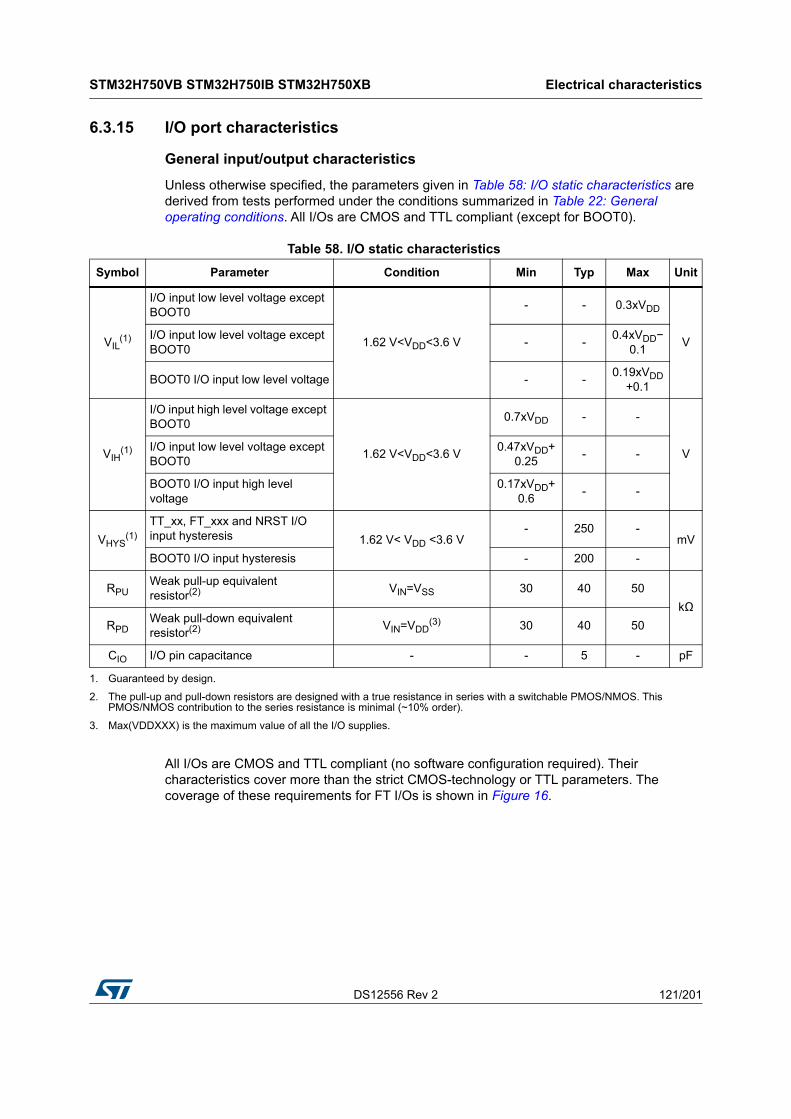
DS12556 Rev 2 121/201
STM32H750VB STM32H750IB STM32H750XB Electrical characteristics
189
6.3.15 I/O port characteristics
General input/output characteristics
Unless otherwise specified, the parameters given in Table 58: I/O static characteristics are derived from tests performed under the conditions summarized in Table 22: General operating conditions. All I/Os are CMOS and TTL compliant (except for BOOT0).
All I/Os are CMOS and TTL compliant (no software configuration required). Their characteristics cover more than the strict CMOS-technology or TTL parameters. The coverage of these requirements for FT I/Os is shown in Figure 16.
Table 58. I/O static characteristics
Symbol Parameter Condition Min Typ Max Unit
VIL(1)
I/O input low level voltage except BOOT0
1.62 V<VDD<3.6 V
- - 0.3xVDD
VI/O input low level voltage except BOOT0
- -0.4xVDD−
0.1
BOOT0 I/O input low level voltage - -0.19xVDD
+0.1
VIH(1)
I/O input high level voltage except BOOT0
1.62 V<VDD<3.6 V
0.7xVDD - -
VI/O input low level voltage except BOOT0
0.47xVDD+0.25
- -
BOOT0 I/O input high level voltage
0.17xVDD+0.6
- -
VHYS(1)
TT_xx, FT_xxx and NRST I/O input hysteresis 1.62 V< VDD <3.6 V
- 250 -mV
BOOT0 I/O input hysteresis - 200 -
RPUWeak pull-up equivalent resistor(2) VIN=VSS 30 40 50
kΩ
RPDWeak pull-down equivalent resistor(2) VIN=VDD
(3) 30 40 50
CIO I/O pin capacitance - - 5 - pF
1. Guaranteed by design.
2. The pull-up and pull-down resistors are designed with a true resistance in series with a switchable PMOS/NMOS. This PMOS/NMOS contribution to the series resistance is minimal (~10% order).
3. Max(VDDXXX) is the maximum value of all the I/O supplies.

Electrical characteristics STM32H750VB STM32H750IB STM32H750XB
122/201 DS12556 Rev 2
Figure 16. VIL/VIH for all I/Os except BOOT0
Output driving current
The GPIOs (general purpose input/outputs) can sink or source up to ±8 mA, and sink or source up to ±20 mA (with a relaxed VOL/VOH).
In the user application, the number of I/O pins which can drive current must be limited to respect the absolute maximum rating specified in Section 6.2. In particular:
• The sum of the currents sourced by all the I/Os on VDD, plus the maximum Run consumption of the MCU sourced on VDD, cannot exceed the absolute maximum rating ΣIVDD (see Table 20).
• The sum of the currents sunk by all the I/Os on VSS plus the maximum Run consumption of the MCU sunk on VSS cannot exceed the absolute maximum rating ΣIVSS (see Table 20).
MSv46121V2
0
0.5
1
1.5
2
2.5
3
1.6 1.8 2 2.2 2.4 2.6 2.8 3 3.2 3.4 3.6
Volta
ge
TLL requirement: VIHmin = 2 V
TLL requirement: VILmin = 0.8 V
CMOS requirement: VIHmin=0.7VDD
CMOS requirement: VILmax=0.3VDD
Based on simulation VIHmin=0.47VDD+0.25
Based on simulation VILmax=0.4VDD+0.1
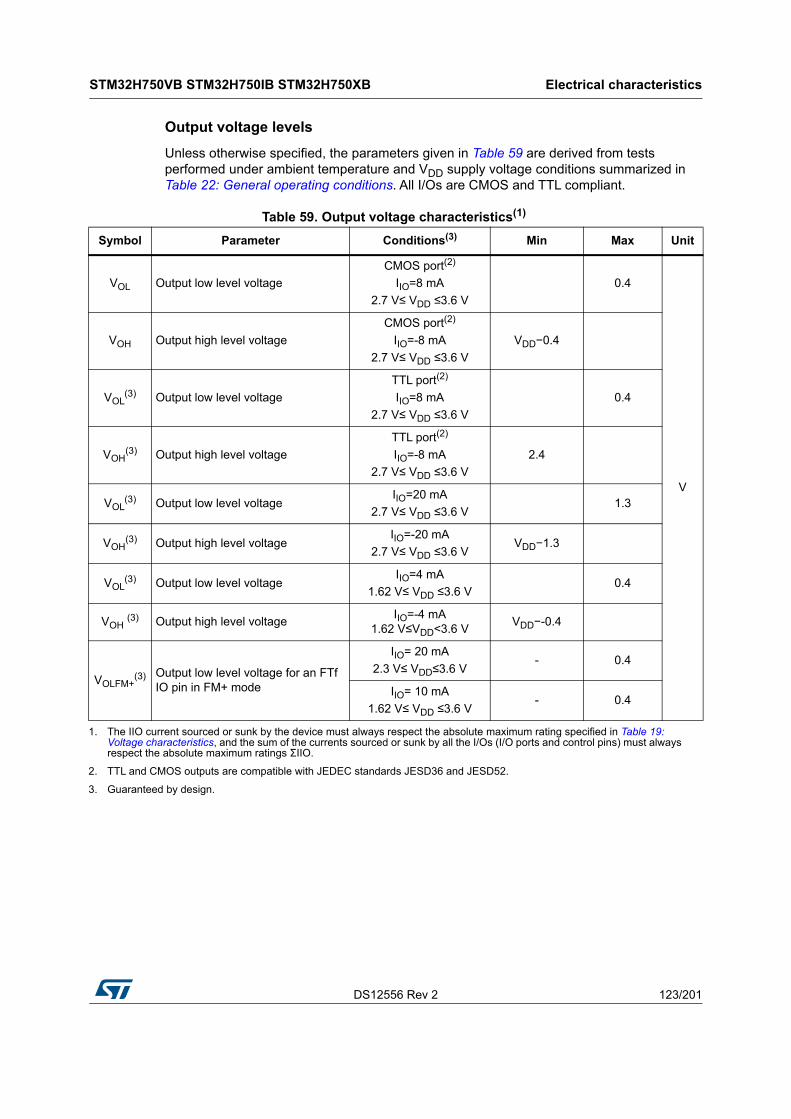
DS12556 Rev 2 123/201
STM32H750VB STM32H750IB STM32H750XB Electrical characteristics
189
Output voltage levels
Unless otherwise specified, the parameters given in Table 59 are derived from tests performed under ambient temperature and VDD supply voltage conditions summarized in Table 22: General operating conditions. All I/Os are CMOS and TTL compliant.
Table 59. Output voltage characteristics(1)
Symbol Parameter Conditions(3) Min Max Unit
VOL Output low level voltage
CMOS port(2)
IIO=8 mA
2.7 V≤ VDD ≤3.6 V
0.4
V
VOH Output high level voltage
CMOS port(2)
IIO=-8 mA
2.7 V≤ VDD ≤3.6 V
VDD−0.4
VOL(3) Output low level voltage
TTL port(2)
IIO=8 mA
2.7 V≤ VDD ≤3.6 V
0.4
VOH(3) Output high level voltage
TTL port(2)
IIO=-8 mA
2.7 V≤ VDD ≤3.6 V
2.4
VOL(3) Output low level voltage
IIO=20 mA
2.7 V≤ VDD ≤3.6 V1.3
VOH(3) Output high level voltage
IIO=-20 mA
2.7 V≤ VDD ≤3.6 VVDD−1.3
VOL(3) Output low level voltage
IIO=4 mA
1.62 V≤ VDD ≤3.6 V0.4
VOH (3) Output high level voltageIIO=-4 mA
1.62 V≤VDD<3.6 VVDD−-0.4
VOLFM+(3) Output low level voltage for an FTf
IO pin in FM+ mode
IIO= 20 mA
2.3 V≤ VDD≤3.6 V- 0.4
IIO= 10 mA
1.62 V≤ VDD ≤3.6 V- 0.4
1. The IIO current sourced or sunk by the device must always respect the absolute maximum rating specified in Table 19: Voltage characteristics, and the sum of the currents sourced or sunk by all the I/Os (I/O ports and control pins) must always respect the absolute maximum ratings ΣIIO.
2. TTL and CMOS outputs are compatible with JEDEC standards JESD36 and JESD52.
3. Guaranteed by design.

Electrical characteristics STM32H750VB STM32H750IB STM32H750XB
124/201 DS12556 Rev 2
Output buffer timing characteristics (HSLV option disabled)
The HSLV bit of SYSCFG_CCCSR register can be used to optimize the I/O speed when the product voltage is below 2.5 V.
Table 60. Output timing characteristics (HSLV OFF)(1)
Speed Symbol Parameter conditions Min Max Unit
00
Fmax(2) Maximum frequency
C=50 pF, 2.7 V≤ VDD≤3.6 V - 12
MHz
C=50 pF, 1.62 V≤VDD≤2.7 V - 3
C=30 pF, 2.7 V≤VDD≤3.6 V - 12
C=30 pF, 1.62 V≤VDD≤2.7 V - 3
C=10 pF, 2.7 V≤VDD≤3.6 V - 16
C=10 pF, 1.62 V≤VDD≤2.7 V - 4
tr/tf(3)
Output high to low level fall time and output low to high level rise time
C=50 pF, 2.7 V≤ VDD≤3.6 V - 16.6
ns
C=50 pF, 1.62 V≤VDD≤2.7 V - 33.3
C=30 pF, 2.7 V≤VDD≤3.6 V - 13.3
C=30 pF, 1.62 V≤VDD≤2.7 V - 25
C=10 pF, 2.7 V≤VDD≤3.6 V - 10
C=10 pF, 1.62 V≤VDD≤2.7 V - 20
01
Fmax(2) Maximum frequency
C=50 pF, 2.7 V≤ VDD≤3.6 V - 60
MHz
C=50 pF, 1.62 V≤VDD≤2.7 V - 15
C=30 pF, 2.7 V≤VDD≤3.6 V - 80
C=30 pF, 1.62 V≤VDD≤2.7 V - 15
C=10 pF, 2.7 V≤VDD≤3.6 V - 110
C=10 pF, 1.62 V≤VDD≤2.7 V - 20
tr/tf(3)
Output high to low level fall time and output low to high level rise time
C=50 pF, 2.7 V≤ VDD≤3.6 V - 5.2
ns
C=50 pF, 1.62 V≤VDD≤2.7 V - 10
C=30 pF, 2.7 V≤VDD≤3.6 V - 4.2
C=30 pF, 1.62 V≤VDD≤2.7 V - 7.5
C=10 pF, 2.7 V≤VDD≤3.6 V - 2.8
C=10 pF, 1.62 V≤VDD≤2.7 V - 5.2

DS12556 Rev 2 125/201
STM32H750VB STM32H750IB STM32H750XB Electrical characteristics
189
10
Fmax(2) Maximum frequency
C=50 pF, 2.7 V≤VDD≤3.6 V(4) - 85
MHz
C=50 pF, 1.62 V≤VDD≤2.7 V(4) - 35
C=30 pF, 2.7 V≤VDD≤3.6 V(4) - 110
C=30 pF, 1.62 V≤VDD≤2.7 V(4) - 40
C=10 pF, 2.7 V≤VDD≤3.6 V(4) - 166
C=10 pF, 1.62 V≤VDD≤2.7 V(4) - 100
tr/tf(3)
Output high to low level fall time and output low to high level rise time
C=50 pF, 2.7 V≤VDD≤3.6 V(4) - 3.8
ns
C=50 pF, 1.62 V≤VDD≤2.7 V(4) - 6.9
C=30 pF, 2.7 V≤VDD≤3.6 V(4) - 2.8
C=30 pF, 1.62 V≤VDD≤2.7 V(4) - 5.2
C=10 pF, 2.7 V≤VDD≤3.6 V(4) - 1.8
C=10 pF, 1.62 V≤VDD≤2.7 V(4) - 3.3
11
Fmax(2) Maximum frequency
C=50 pF, 2.7 V≤VDD≤3.6 V(4) - 100
MHz
C=50 pF, 1.62 V≤VDD≤2.7 V(4) - 50
C=30 pF, 2.7 V≤VDD≤3.6 V(4) - 133
C=30 pF, 1.62 V≤VDD≤2.7 V(4) - 66
C=10 pF, 2.7 V≤VDD≤3.6 V(4) - 220
C=10 pF, 1.62 V≤VDD≤2.7 V(4) - 85
tr/tf(3)
Output high to low level fall time and output low to high level rise time
C=50 pF, 2.7 V≤VDD≤3.6 V(4) - 3.3
ns
C=50 pF, 1.62 V≤VDD≤2.7 V(4) - 6.6
C=30 pF, 2.7 V≤VDD≤3.6 V(4) - 2.4
C=30 pF, 1.62 V≤VDD≤2.7 V(4) - 4.5
C=10 pF, 2.7 V≤VDD≤3.6 V(4) - 1.5
C=10 pF, 1.62 V≤VDD≤2.7 V(4) - 2.7
1. Guaranteed by design.
2. The maximum frequency is defined with the following conditions: (tr+tf) ≤ 2/3 T Skew ≤ 1/20 T 45%<Duty cycle<55%
3. The fall and rise times are defined between 90% and 10% and between 10% and 90% of the output waveform, respectively.
4. Compensation system enabled.
Table 60. Output timing characteristics (HSLV OFF)(1) (continued)
Speed Symbol Parameter conditions Min Max Unit
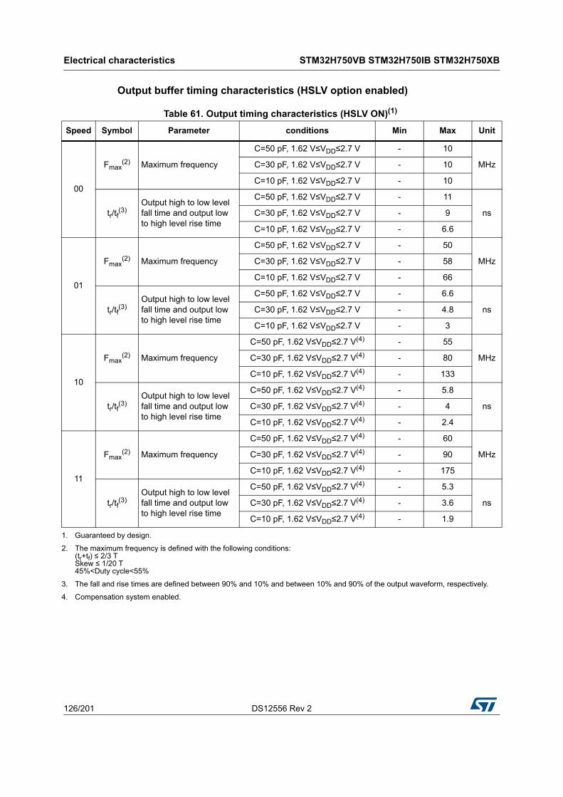
Electrical characteristics STM32H750VB STM32H750IB STM32H750XB
126/201 DS12556 Rev 2
Output buffer timing characteristics (HSLV option enabled)
Table 61. Output timing characteristics (HSLV ON)(1)
Speed Symbol Parameter conditions Min Max Unit
00
Fmax(2) Maximum frequency
C=50 pF, 1.62 V≤VDD≤2.7 V - 10
MHzC=30 pF, 1.62 V≤VDD≤2.7 V - 10
C=10 pF, 1.62 V≤VDD≤2.7 V - 10
tr/tf(3)
Output high to low level fall time and output low to high level rise time
C=50 pF, 1.62 V≤VDD≤2.7 V - 11
nsC=30 pF, 1.62 V≤VDD≤2.7 V - 9
C=10 pF, 1.62 V≤VDD≤2.7 V - 6.6
01
Fmax(2) Maximum frequency
C=50 pF, 1.62 V≤VDD≤2.7 V - 50
MHzC=30 pF, 1.62 V≤VDD≤2.7 V - 58
C=10 pF, 1.62 V≤VDD≤2.7 V - 66
tr/tf(3)
Output high to low level fall time and output low to high level rise time
C=50 pF, 1.62 V≤VDD≤2.7 V - 6.6
nsC=30 pF, 1.62 V≤VDD≤2.7 V - 4.8
C=10 pF, 1.62 V≤VDD≤2.7 V - 3
10
Fmax(2) Maximum frequency
C=50 pF, 1.62 V≤VDD≤2.7 V(4) - 55
MHzC=30 pF, 1.62 V≤VDD≤2.7 V(4) - 80
C=10 pF, 1.62 V≤VDD≤2.7 V(4) - 133
tr/tf(3)
Output high to low level fall time and output low to high level rise time
C=50 pF, 1.62 V≤VDD≤2.7 V(4) - 5.8
nsC=30 pF, 1.62 V≤VDD≤2.7 V(4) - 4
C=10 pF, 1.62 V≤VDD≤2.7 V(4) - 2.4
11
Fmax(2) Maximum frequency
C=50 pF, 1.62 V≤VDD≤2.7 V(4) - 60
MHzC=30 pF, 1.62 V≤VDD≤2.7 V(4) - 90
C=10 pF, 1.62 V≤VDD≤2.7 V(4) - 175
tr/tf(3)
Output high to low level fall time and output low to high level rise time
C=50 pF, 1.62 V≤VDD≤2.7 V(4) - 5.3
nsC=30 pF, 1.62 V≤VDD≤2.7 V(4) - 3.6
C=10 pF, 1.62 V≤VDD≤2.7 V(4) - 1.9
1. Guaranteed by design.
2. The maximum frequency is defined with the following conditions: (tr+tf) ≤ 2/3 T Skew ≤ 1/20 T 45%<Duty cycle<55%
3. The fall and rise times are defined between 90% and 10% and between 10% and 90% of the output waveform, respectively.
4. Compensation system enabled.

DS12556 Rev 2 127/201
STM32H750VB STM32H750IB STM32H750XB Electrical characteristics
189
6.3.16 NRST pin characteristics
The NRST pin input driver uses CMOS technology. It is connected to a permanent pull-up resistor, RPU (see Table 58: I/O static characteristics).
Unless otherwise specified, the parameters given in Table 62 are derived from tests performed under the ambient temperature and VDD supply voltage conditions summarized in Table 22: General operating conditions.
Figure 17. Recommended NRST pin protection
1. The reset network protects the device against parasitic resets.
2. The user must ensure that the level on the NRST pin can go below the VIL(NRST) max level specified in Table 62. Otherwise the reset is not taken into account by the device.
Table 62. NRST pin characteristics
Symbol Parameter Conditions Min Typ Max Unit
RPU(2) Weak pull-up equivalent
resistor(1)
1. The pull-up is designed with a true resistance in series with a switchable PMOS. This PMOS contribution to the series resistance must be minimum (~10% order).
VIN = VSS 30 40 50
VF(NRST)(2)
2. Guaranteed by design.
NRST Input filtered pulse 1.71 V < VDD < 3.6 V - - 50
nsVNF(NRST)
(2) NRST Input not filtered pulse1.71 V < VDD < 3.6 V 300 - -
1.62 V < VDD < 3.6 V 1000 - -
ai14132d
STM32
RPUNRST(2)
VDD
Filter
Internal Reset
0.1 μF
Externalreset circuit (1)
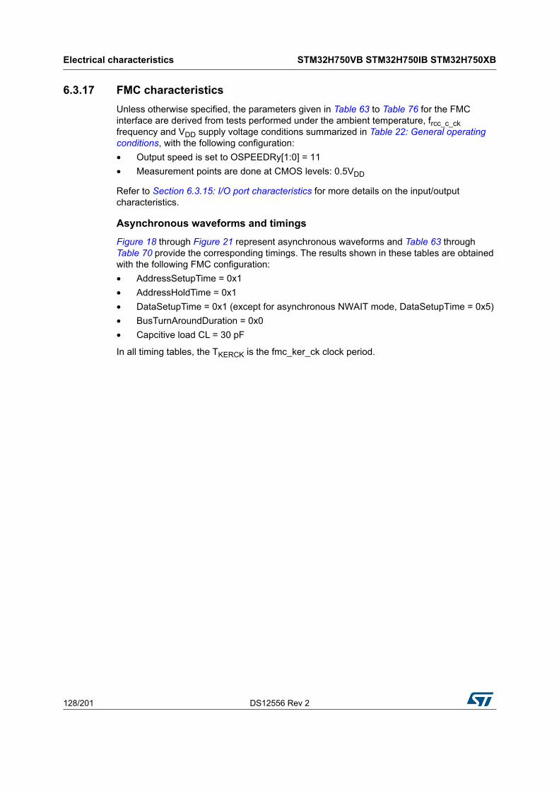
Electrical characteristics STM32H750VB STM32H750IB STM32H750XB
128/201 DS12556 Rev 2
6.3.17 FMC characteristics
Unless otherwise specified, the parameters given in Table 63 to Table 76 for the FMC interface are derived from tests performed under the ambient temperature, frcc_c_ck frequency and VDD supply voltage conditions summarized in Table 22: General operating conditions, with the following configuration:
• Output speed is set to OSPEEDRy[1:0] = 11
• Measurement points are done at CMOS levels: 0.5VDD
Refer to Section 6.3.15: I/O port characteristics for more details on the input/output characteristics.
Asynchronous waveforms and timings
Figure 18 through Figure 21 represent asynchronous waveforms and Table 63 through Table 70 provide the corresponding timings. The results shown in these tables are obtained with the following FMC configuration:
• AddressSetupTime = 0x1
• AddressHoldTime = 0x1
• DataSetupTime = 0x1 (except for asynchronous NWAIT mode, DataSetupTime = 0x5)
• BusTurnAroundDuration = 0x0
• Capcitive load CL = 30 pF
In all timing tables, the TKERCK is the fmc_ker_ck clock period.

DS12556 Rev 2 129/201
STM32H750VB STM32H750IB STM32H750XB Electrical characteristics
189
Figure 18. Asynchronous non-multiplexed SRAM/PSRAM/NOR read waveforms
1. Mode 2/B, C and D only. In Mode 1, FMC_NADV is not used.
Data
FMC_NE
FMC_NBL[1:0]
FMC_D[15:0]
tv(BL_NE)
t h(Data_NE)
FMC_NOE
AddressFMC_A[25:0]
tv(A_NE)
FMC_NWE
tsu(Data_NE)
tw(NE)
MS32753V1
w(NOE)ttv(NOE_NE) t h(NE_NOE)
th(Data_NOE)
t h(A_NOE)
t h(BL_NOE)
tsu(Data_NOE)
FMC_NADV (1)
t v(NADV_NE)
tw(NADV)
FMC_NWAIT
tsu(NWAIT_NE)
th(NE_NWAIT)
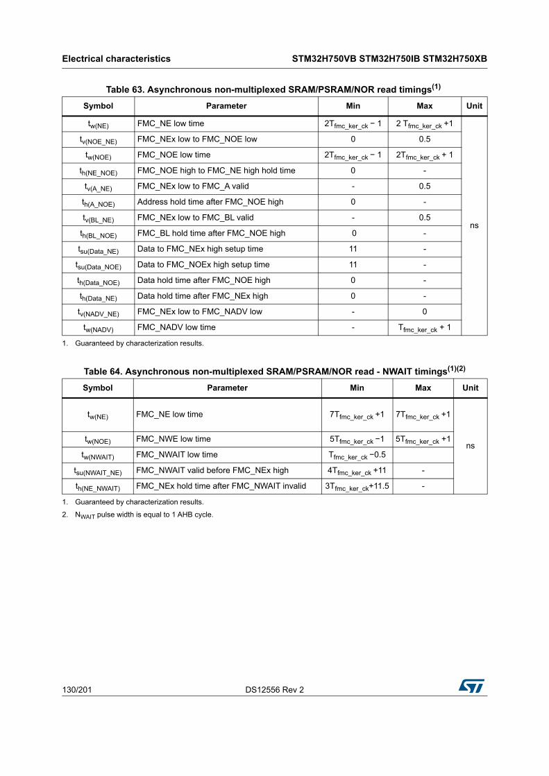
Electrical characteristics STM32H750VB STM32H750IB STM32H750XB
130/201 DS12556 Rev 2
Table 63. Asynchronous non-multiplexed SRAM/PSRAM/NOR read timings(1)
Symbol Parameter Min Max Unit
tw(NE) FMC_NE low time 2Tfmc_ker_ck − 1 2 Tfmc_ker_ck +1
ns
tv(NOE_NE) FMC_NEx low to FMC_NOE low 0 0.5
tw(NOE) FMC_NOE low time 2Tfmc_ker_ck − 1 2Tfmc_ker_ck + 1
th(NE_NOE) FMC_NOE high to FMC_NE high hold time 0 -
tv(A_NE) FMC_NEx low to FMC_A valid - 0.5
th(A_NOE) Address hold time after FMC_NOE high 0 -
tv(BL_NE) FMC_NEx low to FMC_BL valid - 0.5
th(BL_NOE) FMC_BL hold time after FMC_NOE high 0 -
tsu(Data_NE) Data to FMC_NEx high setup time 11 -
tsu(Data_NOE) Data to FMC_NOEx high setup time 11 -
th(Data_NOE) Data hold time after FMC_NOE high 0 -
th(Data_NE) Data hold time after FMC_NEx high 0 -
tv(NADV_NE) FMC_NEx low to FMC_NADV low - 0
tw(NADV) FMC_NADV low time - Tfmc_ker_ck + 1
1. Guaranteed by characterization results.
Table 64. Asynchronous non-multiplexed SRAM/PSRAM/NOR read - NWAIT timings(1)(2)
Symbol Parameter Min Max Unit
tw(NE) FMC_NE low time 7Tfmc_ker_ck +1 7Tfmc_ker_ck +1
nstw(NOE) FMC_NWE low time 5Tfmc_ker_ck −1 5Tfmc_ker_ck +1
tw(NWAIT) FMC_NWAIT low time Tfmc_ker_ck −0.5
tsu(NWAIT_NE) FMC_NWAIT valid before FMC_NEx high 4Tfmc_ker_ck +11 -
th(NE_NWAIT) FMC_NEx hold time after FMC_NWAIT invalid 3Tfmc_ker_ck+11.5 -
1. Guaranteed by characterization results.
2. NWAIT pulse width is equal to 1 AHB cycle.
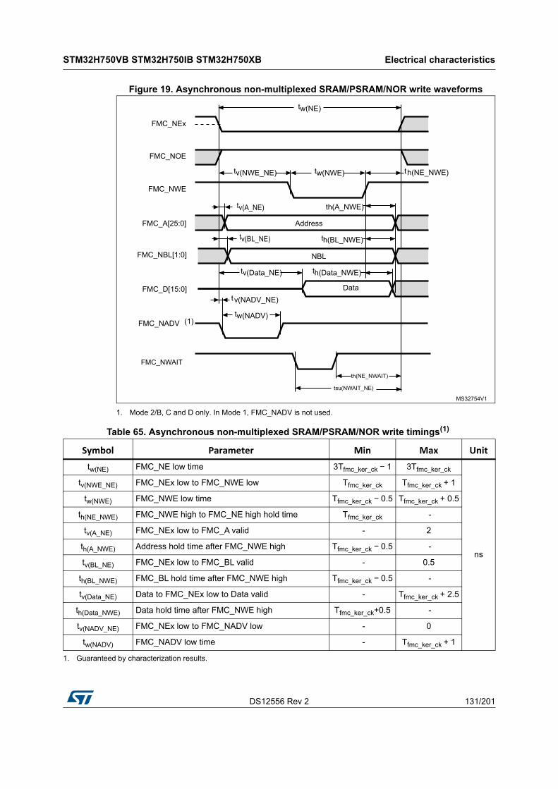
DS12556 Rev 2 131/201
STM32H750VB STM32H750IB STM32H750XB Electrical characteristics
189
Figure 19. Asynchronous non-multiplexed SRAM/PSRAM/NOR write waveforms
1. Mode 2/B, C and D only. In Mode 1, FMC_NADV is not used.
NBL
Data
FMC_NEx
FMC_NBL[1:0]
FMC_D[15:0]
tv(BL_NE)
th(Data_NWE)
FMC_NOE
AddressFMC_A[25:0]
tv(A_NE)
tw(NWE)
FMC_NWE
tv(NWE_NE) th(NE_NWE)
th(A_NWE)
th(BL_NWE)
tv(Data_NE)
tw(NE)
MS32754V1
FMC_NADV (1)
tv(NADV_NE)
tw(NADV)
FMC_NWAIT
tsu(NWAIT_NE)
th(NE_NWAIT)
Table 65. Asynchronous non-multiplexed SRAM/PSRAM/NOR write timings(1)
Symbol Parameter Min Max Unit
tw(NE) FMC_NE low time 3Tfmc_ker_ck − 1 3Tfmc_ker_ck
ns
tv(NWE_NE) FMC_NEx low to FMC_NWE low Tfmc_ker_ck Tfmc_ker_ck + 1
tw(NWE) FMC_NWE low time Tfmc_ker_ck − 0.5 Tfmc_ker_ck + 0.5
th(NE_NWE) FMC_NWE high to FMC_NE high hold time Tfmc_ker_ck -
tv(A_NE) FMC_NEx low to FMC_A valid - 2
th(A_NWE) Address hold time after FMC_NWE high Tfmc_ker_ck − 0.5 -
tv(BL_NE) FMC_NEx low to FMC_BL valid - 0.5
th(BL_NWE) FMC_BL hold time after FMC_NWE high Tfmc_ker_ck − 0.5 -
tv(Data_NE) Data to FMC_NEx low to Data valid - Tfmc_ker_ck + 2.5
th(Data_NWE) Data hold time after FMC_NWE high Tfmc_ker_ck+0.5 -
tv(NADV_NE) FMC_NEx low to FMC_NADV low - 0
tw(NADV) FMC_NADV low time - Tfmc_ker_ck + 1
1. Guaranteed by characterization results.
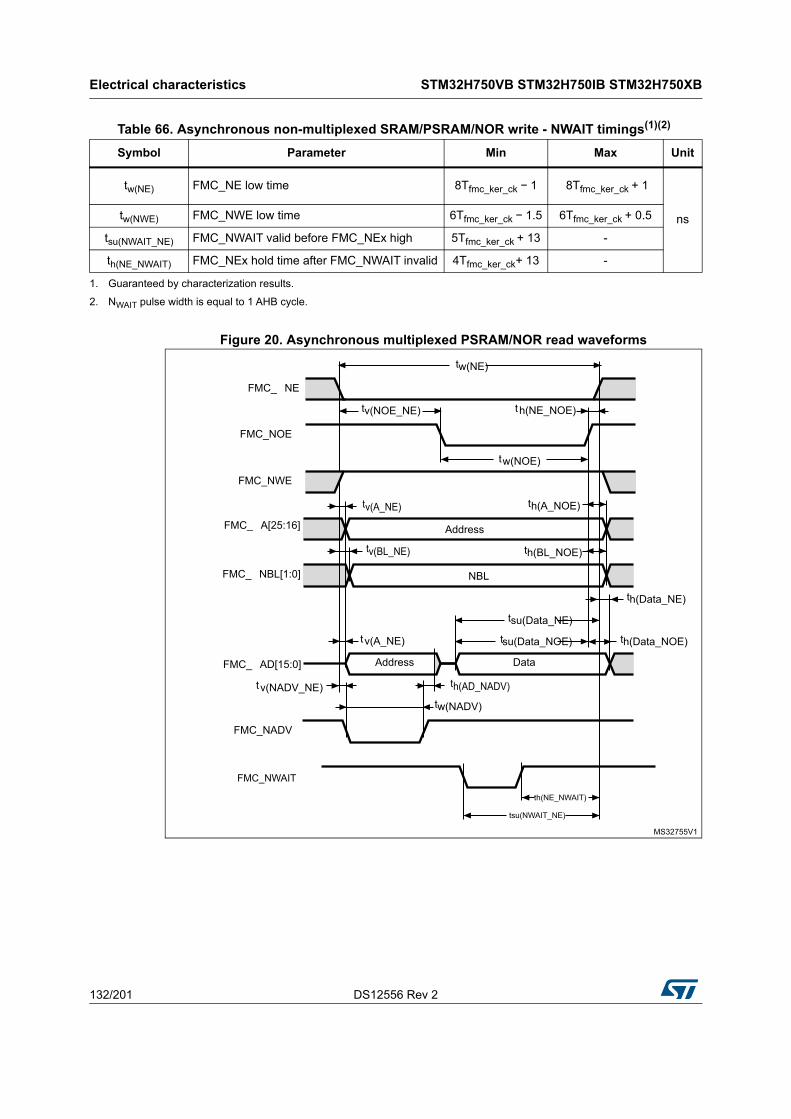
Electrical characteristics STM32H750VB STM32H750IB STM32H750XB
132/201 DS12556 Rev 2
Figure 20. Asynchronous multiplexed PSRAM/NOR read waveforms
Table 66. Asynchronous non-multiplexed SRAM/PSRAM/NOR write - NWAIT timings(1)(2)
Symbol Parameter Min Max Unit
tw(NE) FMC_NE low time 8Tfmc_ker_ck − 1 8Tfmc_ker_ck + 1
nstw(NWE) FMC_NWE low time 6Tfmc_ker_ck − 1.5 6Tfmc_ker_ck + 0.5
tsu(NWAIT_NE) FMC_NWAIT valid before FMC_NEx high 5Tfmc_ker_ck + 13 -
th(NE_NWAIT) FMC_NEx hold time after FMC_NWAIT invalid 4Tfmc_ker_ck+ 13 -
1. Guaranteed by characterization results.
2. NWAIT pulse width is equal to 1 AHB cycle.
NBL
Data
FMC_ NBL[1:0]
FMC_ AD[15:0]
tv(BL_NE)
th(Data_NE)
AddressFMC_ A[25:16]
tv(A_NE)
FMC_NWE
tv(A_NE)
MS32755V1
Address
FMC_NADV
tv(NADV_NE)tw(NADV)
tsu(Data_NE)
th(AD_NADV)
FMC_ NE
FMC_NOE
tw(NE)
tw(NOE)
tv(NOE_NE) th(NE_NOE)
th(A_NOE)
th(BL_NOE)
tsu(Data_NOE) th(Data_NOE)
FMC_NWAIT
tsu(NWAIT_NE)
th(NE_NWAIT)
DS12556 Rev 2 133/201
STM32H750VB STM32H750IB STM32H750XB Electrical characteristics
189
Table 67. Asynchronous multiplexed PSRAM/NOR read timings(1)
Symbol Parameter Min Max Unit
tw(NE) FMC_NE low time 3Tfmc_ker_ck − 1 3Tfmc_ker_ck + 1
ns
tv(NOE_NE) FMC_NEx low to FMC_NOE low 2Tfmc_ker_ck 2Tfmc_ker_ck + 0.5
ttw(NOE) FMC_NOE low time Tfmc_ker_ck − 1 Tfmc_ker_ck + 1
th(NE_NOE) FMC_NOE high to FMC_NE high hold time 0 -
tv(A_NE) FMC_NEx low to FMC_A valid - 0.5
tv(NADV_NE) FMC_NEx low to FMC_NADV low 0 0.5
tw(NADV) FMC_NADV low time Tfmc_ker_ck − 0.5 Tfmc_ker_ck+1
th(AD_NADV)FMC_AD(address) valid hold time after FMC_NADV high
Tfmc_ker_ck + 0.5 -
th(A_NOE) Address hold time after FMC_NOE high Tfmc_ker_ck − 0.5 -
th(BL_NOE) FMC_BL time after FMC_NOE high 0 -
tv(BL_NE) FMC_NEx low to FMC_BL valid - 0.5
tsu(Data_NE) Data to FMC_NEx high setup time Tfmc_ker_ck − 2 -
tsu(Data_NOE) Data to FMC_NOE high setup time Tfmc_ker_ck − 2 -
th(Data_NE) Data hold time after FMC_NEx high 0 -
th(Data_NOE) Data hold time after FMC_NOE high 0 -
1. Guaranteed by characterization results.
Table 68. Asynchronous multiplexed PSRAM/NOR read-NWAIT timings(1)
Symbol Parameter Min Max Unit
tw(NE) FMC_NE low time 8Tfmc_ker_ck − 1 8Tfmc_ker_ck
nstw(NOE) FMC_NWE low time 5Tfmc_ker_ck − 1.5 5Tfmc_ker_ck + 0.5
tsu(NWAIT_NE) FMC_NWAIT valid before FMC_NEx high 5Tfmc_ker_ck + 3 -
th(NE_NWAIT)FMC_NEx hold time after FMC_NWAIT invalid
4Tfmc_ker_ck -
1. Guaranteed by characterization results.

Electrical characteristics STM32H750VB STM32H750IB STM32H750XB
134/201 DS12556 Rev 2
Figure 21. Asynchronous multiplexed PSRAM/NOR write waveforms
NBL
Data
FMC_ NEx
FMC_ NBL[1:0]
FMC_ AD[15:0]
tv(BL_NE)
th(Data_NWE)
FMC_NOE
AddressFMC_ A[25:16]
tv(A_NE)
tw(NWE)
FMC_NWE
tv(NWE_NE) th(NE_NWE)
th(A_NWE)
th(BL_NWE)
tv(A_NE)
tw(NE)
MS32756V1
Address
FMC_NADV
tv(NADV_NE)
tw(NADV)
tv(Data_NADV)
th(AD_NADV)
FMC_NWAIT
tsu(NWAIT_NE)
th(NE_NWAIT)
Table 69. Asynchronous multiplexed PSRAM/NOR write timings(1)
Symbol Parameter Min Max Unit
tw(NE) FMC_NE low time 4Tfmc_ker_c − 1 4Tfmc_ker_ck
ns
tv(NWE_NE) FMC_NEx low to FMC_NWE low Tfmc_ker_c − 1 Tfmc_ker_ck + 0.5
tw(NWE) FMC_NWE low time 2Tfmc_ker_ck− 0.5 2Tfmc_ker_ck+ 0.5
th(NE_NWE) FMC_NWE high to FMC_NE high hold time Tfmc_ker_ck − 0.5 -
tv(A_NE) FMC_NEx low to FMC_A valid - 0
tv(NADV_NE) FMC_NEx low to FMC_NADV low 0 0.5
tw(NADV) FMC_NADV low time Tfmc_ker_ck Tfmc_ker_ck+ 1
th(AD_NADV) FMC_AD(address) valid hold time after FMC_NADV high Tfmc_ker_ck+0.5 -
th(A_NWE) Address hold time after FMC_NWE high Tfmc_ker_ck+0.5 -
th(BL_NWE) FMC_BL hold time after FMC_NWE high Tfmc_ker_ck − 0.5 -
tv(BL_NE) FMC_NEx low to FMC_BL valid - 0.5
tv(Data_NADV) FMC_NADV high to Data valid - Tfmc_ker_ck + 2
th(Data_NWE) Data hold time after FMC_NWE high Tfmc_ker_ck+0.5 -
1. Guaranteed by characterization results.

DS12556 Rev 2 135/201
STM32H750VB STM32H750IB STM32H750XB Electrical characteristics
189
Synchronous waveforms and timings
Figure 22 through Figure 25 represent synchronous waveforms and Table 71 through Table 74 provide the corresponding timings. The results shown in these tables are obtained with the following FMC configuration:
• BurstAccessMode = FMC_BurstAccessMode_Enable
• MemoryType = FMC_MemoryType_CRAM
• WriteBurst = FMC_WriteBurst_Enable
• CLKDivision = 1
• DataLatency = 1 for NOR Flash; DataLatency = 0 for PSRAM
In all the timing tables, the Tfmc_ker_ck is the fmc_ker_ck clock period, with the following FMC_CLK maximum values:
• For 2.7 V<VDD<3.6 V, FMC_CLK =133 MHz at 20 pF
• For 1.8 V<VDD<1.9 V, FMC_CLK =100 MHz at 20 pF
• For 1.62 V<VDD<1.8 V, FMC_CLK =100 MHz at 15 pF
Table 70. Asynchronous multiplexed PSRAM/NOR write-NWAIT timings(1)
Symbol Parameter Min Max Unit
tw(NE) FMC_NE low time 9Tfmc_ker_ck – 1 9Tfmc_ker_ck
nstw(NWE) FMC_NWE low time 7Tfmc_ker_ck – 0.5 7Tfmc_ker_ck + 0.5
tsu(NWAIT_NE) FMC_NWAIT valid before FMC_NEx high 6Tfmc_ker_ck + 3 -
th(NE_NWAIT) FMC_NEx hold time after FMC_NWAIT invalid 4Tfmc_ker_ck -
1. Guaranteed by characterization results.
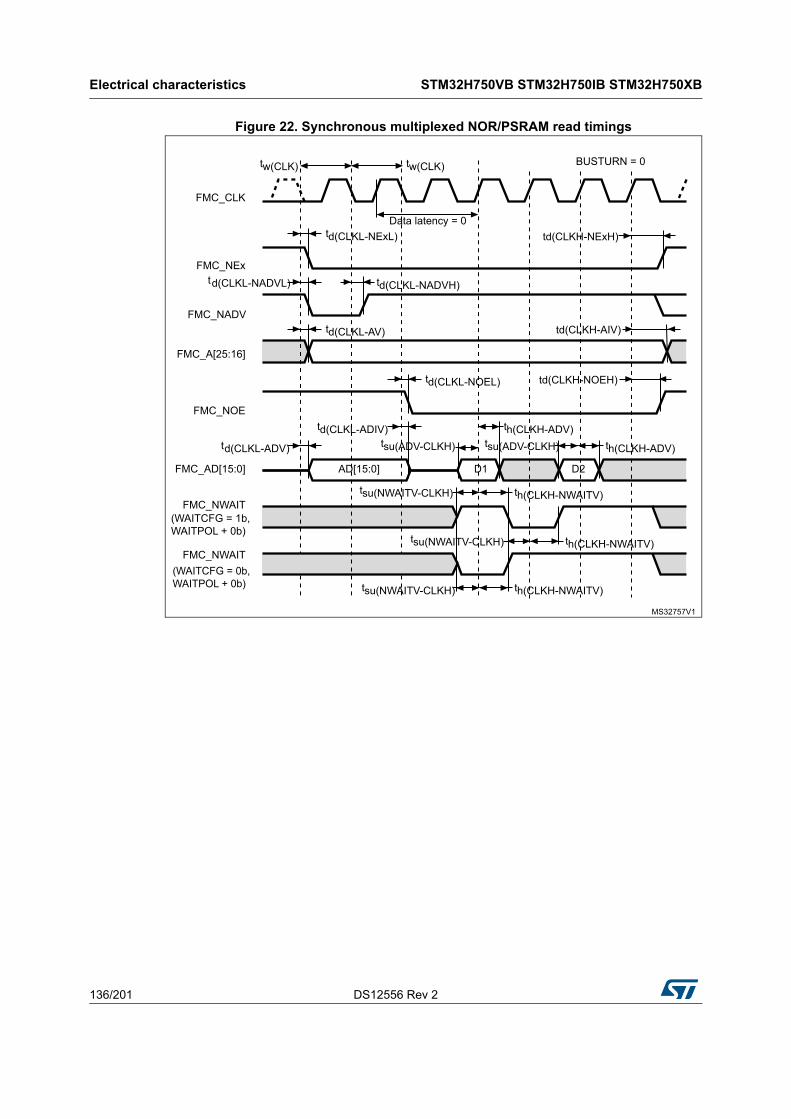
Electrical characteristics STM32H750VB STM32H750IB STM32H750XB
136/201 DS12556 Rev 2
Figure 22. Synchronous multiplexed NOR/PSRAM read timings
FMC_CLK
FMC_NEx
FMC_NADV
FMC_A[25:16]
FMC_NOE
FMC_AD[15:0] AD[15:0] D1 D2
FMC_NWAIT(WAITCFG = 1b, WAITPOL + 0b)
FMC_NWAIT(WAITCFG = 0b, WAITPOL + 0b)
tw(CLK) tw(CLK)
Data latency = 0
BUSTURN = 0
td(CLKL-NExL) td(CLKH-NExH)
td(CLKL-NADVL)
td(CLKL-AV)
td(CLKL-NADVH)
td(CLKH-AIV)
td(CLKL-NOEL) td(CLKH-NOEH)
td(CLKL-ADV)
td(CLKL-ADIV)tsu(ADV-CLKH)
th(CLKH-ADV)tsu(ADV-CLKH) th(CLKH-ADV)
tsu(NWAITV-CLKH) th(CLKH-NWAITV)
tsu(NWAITV-CLKH) th(CLKH-NWAITV)
tsu(NWAITV-CLKH) th(CLKH-NWAITV)
MS32757V1
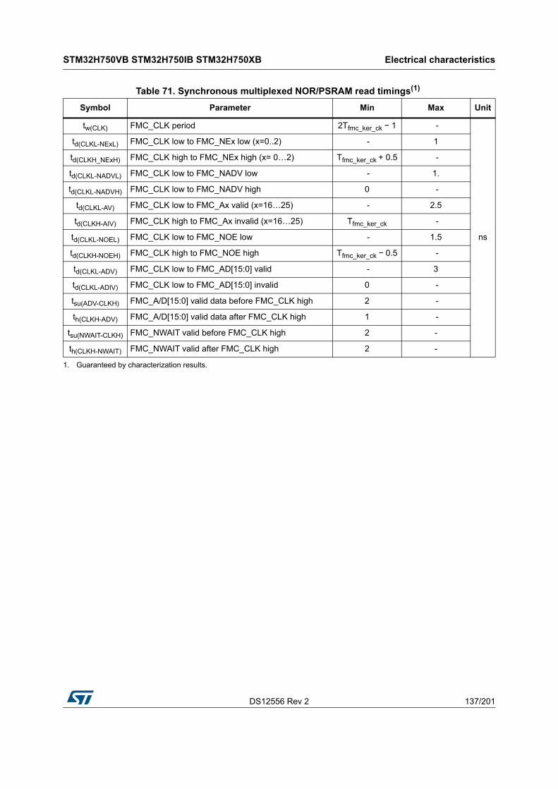
DS12556 Rev 2 137/201
STM32H750VB STM32H750IB STM32H750XB Electrical characteristics
189
Table 71. Synchronous multiplexed NOR/PSRAM read timings(1)
Symbol Parameter Min Max Unit
tw(CLK) FMC_CLK period 2Tfmc_ker_ck − 1 -
ns
td(CLKL-NExL) FMC_CLK low to FMC_NEx low (x=0..2) - 1
td(CLKH_NExH) FMC_CLK high to FMC_NEx high (x= 0…2) Tfmc_ker_ck + 0.5 -
td(CLKL-NADVL) FMC_CLK low to FMC_NADV low - 1.
td(CLKL-NADVH) FMC_CLK low to FMC_NADV high 0 -
td(CLKL-AV) FMC_CLK low to FMC_Ax valid (x=16…25) - 2.5
td(CLKH-AIV) FMC_CLK high to FMC_Ax invalid (x=16…25) Tfmc_ker_ck -
td(CLKL-NOEL) FMC_CLK low to FMC_NOE low - 1.5
td(CLKH-NOEH) FMC_CLK high to FMC_NOE high Tfmc_ker_ck − 0.5 -
td(CLKL-ADV) FMC_CLK low to FMC_AD[15:0] valid - 3
td(CLKL-ADIV) FMC_CLK low to FMC_AD[15:0] invalid 0 -
tsu(ADV-CLKH) FMC_A/D[15:0] valid data before FMC_CLK high 2 -
th(CLKH-ADV) FMC_A/D[15:0] valid data after FMC_CLK high 1 -
tsu(NWAIT-CLKH) FMC_NWAIT valid before FMC_CLK high 2 -
th(CLKH-NWAIT) FMC_NWAIT valid after FMC_CLK high 2 -
1. Guaranteed by characterization results.
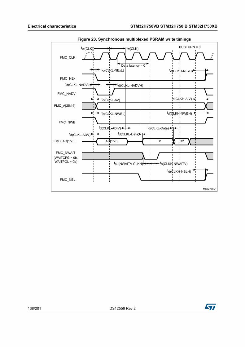
Electrical characteristics STM32H750VB STM32H750IB STM32H750XB
138/201 DS12556 Rev 2
Figure 23. Synchronous multiplexed PSRAM write timings
FMC_CLK
FMC_NEx
FMC_NADV
FMC_A[25:16]
FMC_NWE
FMC_AD[15:0] AD[15:0] D1 D2
FMC_NWAIT(WAITCFG = 0b, WAITPOL + 0b)
tw(CLK) tw(CLK)
Data latency = 0
BUSTURN = 0
td(CLKL-NExL) td(CLKH-NExH)
td(CLKL-NADVL)
td(CLKL-AV)
td(CLKL-NADVH)
td(CLKH-AIV)
td(CLKH-NWEH)td(CLKL-NWEL)
td(CLKH-NBLH)
td(CLKL-ADV)
td(CLKL-ADIV) td(CLKL-Data)
tsu(NWAITV-CLKH) th(CLKH-NWAITV)
MS32758V1
td(CLKL-Data)
FMC_NBL
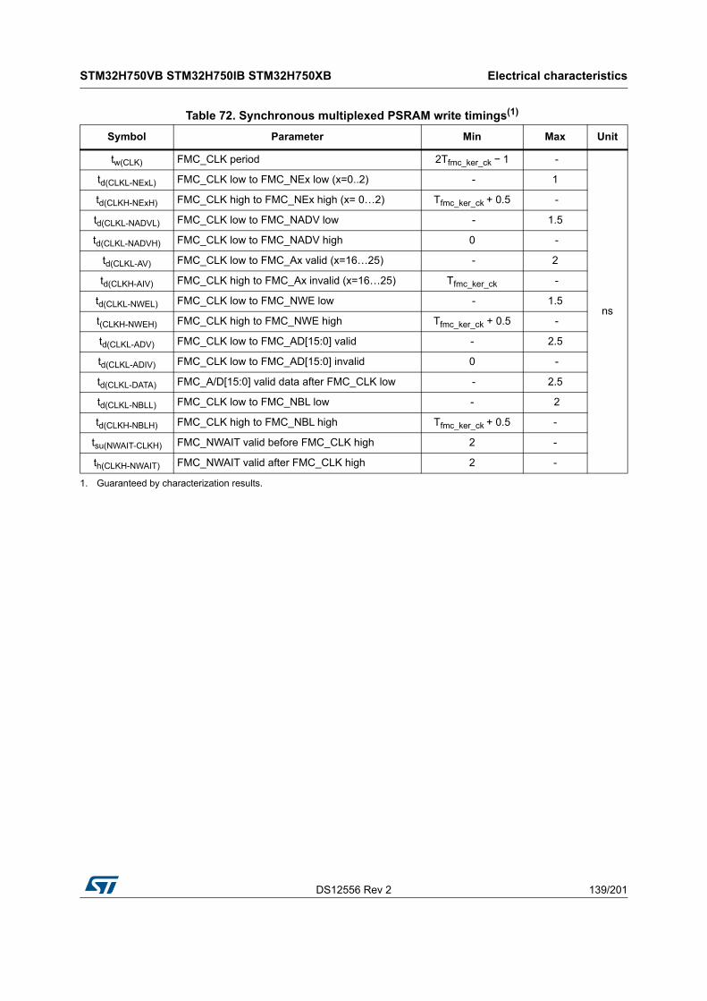
DS12556 Rev 2 139/201
STM32H750VB STM32H750IB STM32H750XB Electrical characteristics
189
Table 72. Synchronous multiplexed PSRAM write timings(1)
Symbol Parameter Min Max Unit
tw(CLK) FMC_CLK period 2Tfmc_ker_ck − 1 -
ns
td(CLKL-NExL) FMC_CLK low to FMC_NEx low (x=0..2) - 1
td(CLKH-NExH) FMC_CLK high to FMC_NEx high (x= 0…2) Tfmc_ker_ck + 0.5 -
td(CLKL-NADVL) FMC_CLK low to FMC_NADV low - 1.5
td(CLKL-NADVH) FMC_CLK low to FMC_NADV high 0 -
td(CLKL-AV) FMC_CLK low to FMC_Ax valid (x=16…25) - 2
td(CLKH-AIV) FMC_CLK high to FMC_Ax invalid (x=16…25) Tfmc_ker_ck -
td(CLKL-NWEL) FMC_CLK low to FMC_NWE low - 1.5
t(CLKH-NWEH) FMC_CLK high to FMC_NWE high Tfmc_ker_ck + 0.5 -
td(CLKL-ADV) FMC_CLK low to FMC_AD[15:0] valid - 2.5
td(CLKL-ADIV) FMC_CLK low to FMC_AD[15:0] invalid 0 -
td(CLKL-DATA) FMC_A/D[15:0] valid data after FMC_CLK low - 2.5
td(CLKL-NBLL) FMC_CLK low to FMC_NBL low - 2
td(CLKH-NBLH) FMC_CLK high to FMC_NBL high Tfmc_ker_ck + 0.5 -
tsu(NWAIT-CLKH) FMC_NWAIT valid before FMC_CLK high 2 -
th(CLKH-NWAIT) FMC_NWAIT valid after FMC_CLK high 2 -
1. Guaranteed by characterization results.
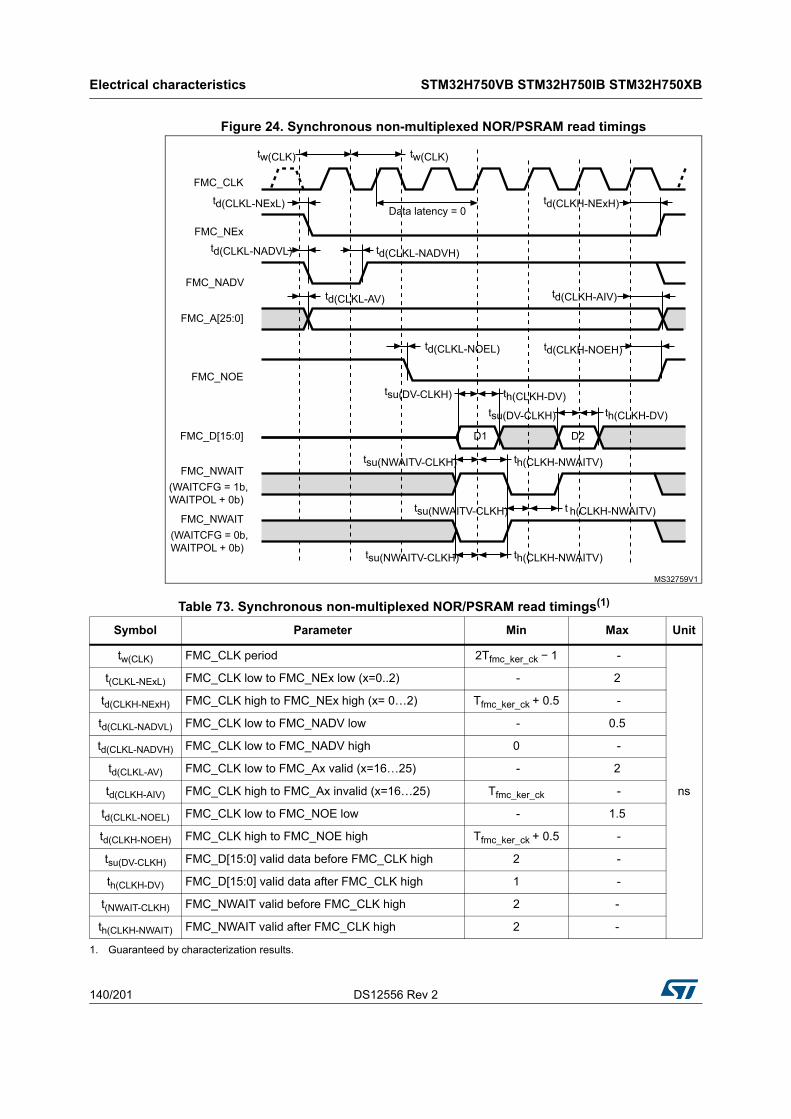
Electrical characteristics STM32H750VB STM32H750IB STM32H750XB
140/201 DS12556 Rev 2
Figure 24. Synchronous non-multiplexed NOR/PSRAM read timings
FMC_CLK
FMC_NEx
FMC_A[25:0]
FMC_NOE
FMC_D[15:0] D1 D2
FMC_NWAIT(WAITCFG = 1b, WAITPOL + 0b)
FMC_NWAIT(WAITCFG = 0b, WAITPOL + 0b)
tw(CLK) tw(CLK)
Data latency = 0td(CLKL-NExL) td(CLKH-NExH)
td(CLKL-AV) td(CLKH-AIV)
td(CLKL-NOEL) td(CLKH-NOEH)
tsu(DV-CLKH) th(CLKH-DV)tsu(DV-CLKH) th(CLKH-DV)
tsu(NWAITV-CLKH) th(CLKH-NWAITV)
tsu(NWAITV-CLKH) t h(CLKH-NWAITV)
tsu(NWAITV-CLKH) th(CLKH-NWAITV)
MS32759V1
FMC_NADV
td(CLKL-NADVL) td(CLKL-NADVH)
Table 73. Synchronous non-multiplexed NOR/PSRAM read timings(1)
Symbol Parameter Min Max Unit
tw(CLK) FMC_CLK period 2Tfmc_ker_ck − 1 -
ns
t(CLKL-NExL) FMC_CLK low to FMC_NEx low (x=0..2) - 2
td(CLKH-NExH) FMC_CLK high to FMC_NEx high (x= 0…2) Tfmc_ker_ck + 0.5 -
td(CLKL-NADVL) FMC_CLK low to FMC_NADV low - 0.5
td(CLKL-NADVH) FMC_CLK low to FMC_NADV high 0 -
td(CLKL-AV) FMC_CLK low to FMC_Ax valid (x=16…25) - 2
td(CLKH-AIV) FMC_CLK high to FMC_Ax invalid (x=16…25) Tfmc_ker_ck -
td(CLKL-NOEL) FMC_CLK low to FMC_NOE low - 1.5
td(CLKH-NOEH) FMC_CLK high to FMC_NOE high Tfmc_ker_ck + 0.5 -
tsu(DV-CLKH) FMC_D[15:0] valid data before FMC_CLK high 2 -
th(CLKH-DV) FMC_D[15:0] valid data after FMC_CLK high 1 -
t(NWAIT-CLKH) FMC_NWAIT valid before FMC_CLK high 2 -
th(CLKH-NWAIT) FMC_NWAIT valid after FMC_CLK high 2 -
1. Guaranteed by characterization results.
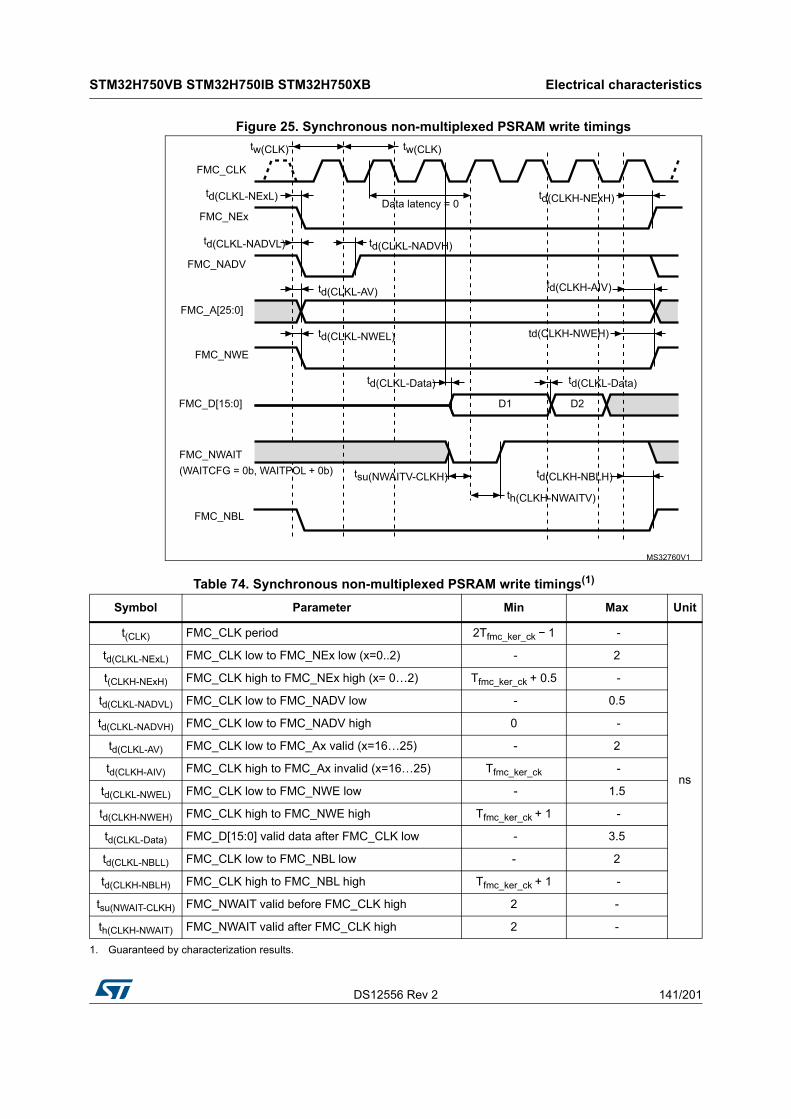
DS12556 Rev 2 141/201
STM32H750VB STM32H750IB STM32H750XB Electrical characteristics
189
Figure 25. Synchronous non-multiplexed PSRAM write timings
MS32760V1
FMC_CLK
FMC_NEx
FMC_A[25:0]
FMC_NWE
FMC_D[15:0] D1 D2
FMC_NWAIT(WAITCFG = 0b, WAITPOL + 0b)
tw(CLK) tw(CLK)
Data latency = 0td(CLKL-NExL) td(CLKH-NExH)
td(CLKL-AV)td(CLKH-AIV)
td(CLKH-NWEH)td(CLKL-NWEL)
td(CLKL-Data)
tsu(NWAITV-CLKH)
th(CLKH-NWAITV)
FMC_NADV
td(CLKL-NADVL) td(CLKL-NADVH)
td(CLKL-Data)
FMC_NBL
td(CLKH-NBLH)
Table 74. Synchronous non-multiplexed PSRAM write timings(1)
Symbol Parameter Min Max Unit
t(CLK) FMC_CLK period 2Tfmc_ker_ck − 1 -
ns
td(CLKL-NExL) FMC_CLK low to FMC_NEx low (x=0..2) - 2
t(CLKH-NExH) FMC_CLK high to FMC_NEx high (x= 0…2) Tfmc_ker_ck + 0.5 -
td(CLKL-NADVL) FMC_CLK low to FMC_NADV low - 0.5
td(CLKL-NADVH) FMC_CLK low to FMC_NADV high 0 -
td(CLKL-AV) FMC_CLK low to FMC_Ax valid (x=16…25) - 2
td(CLKH-AIV) FMC_CLK high to FMC_Ax invalid (x=16…25) Tfmc_ker_ck -
td(CLKL-NWEL) FMC_CLK low to FMC_NWE low - 1.5
td(CLKH-NWEH) FMC_CLK high to FMC_NWE high Tfmc_ker_ck + 1 -
td(CLKL-Data) FMC_D[15:0] valid data after FMC_CLK low - 3.5
td(CLKL-NBLL) FMC_CLK low to FMC_NBL low - 2
td(CLKH-NBLH) FMC_CLK high to FMC_NBL high Tfmc_ker_ck + 1 -
tsu(NWAIT-CLKH) FMC_NWAIT valid before FMC_CLK high 2 -
th(CLKH-NWAIT) FMC_NWAIT valid after FMC_CLK high 2 -
1. Guaranteed by characterization results.

Electrical characteristics STM32H750VB STM32H750IB STM32H750XB
142/201 DS12556 Rev 2
NAND controller waveforms and timings
Figure 26 through Figure 29 represent synchronous waveforms, and Table 75 and Table 76 provide the corresponding timings. The results shown in this table are obtained with the following FMC configuration:
• COM.FMC_SetupTime = 0x01
• COM.FMC_WaitSetupTime = 0x03
• COM.FMC_HoldSetupTime = 0x02
• COM.FMC_HiZSetupTime = 0x01
• ATT.FMC_SetupTime = 0x01
• ATT.FMC_WaitSetupTime = 0x03
• ATT.FMC_HoldSetupTime = 0x02
• ATT.FMC_HiZSetupTime = 0x01
• Bank = FMC_Bank_NAND
• MemoryDataWidth = FMC_MemoryDataWidth_16b
• ECC = FMC_ECC_Enable
• ECCPageSize = FMC_ECCPageSize_512Bytes
• TCLRSetupTime = 0
• TARSetupTime = 0
• CL = 30 pF
In all timing tables, the Tfmc_ker_ck is the fmc_ker_ck clock period.
Figure 26. NAND controller waveforms for read access
FMC_NWE
FMC_NOE (NRE)
FMC_D[15:0]
tsu(D-NOE) th(NOE-D)
MS32767V1
ALE (FMC_A17)CLE (FMC_A16)
FMC_NCEx
td(ALE-NOE) th(NOE-ALE)

DS12556 Rev 2 143/201
STM32H750VB STM32H750IB STM32H750XB Electrical characteristics
189
Figure 27. NAND controller waveforms for write access
Figure 28. NAND controller waveforms for common memory read access
MS32768V1
th(NWE-D)tv(NWE-D)
FMC_NWE
FMC_NOE (NRE)
FMC_D[15:0]
ALE (FMC_A17)CLE (FMC_A16)
FMC_NCEx
td(ALE-NWE) th(NWE-ALE)
MS32769V1
FMC_NWE
FMC_NOE
FMC_D[15:0]
tw(NOE)
tsu(D-NOE) th(NOE-D)
ALE (FMC_A17)CLE (FMC_A16)
FMC_NCEx
td(ALE-NOE) th(NOE-ALE)
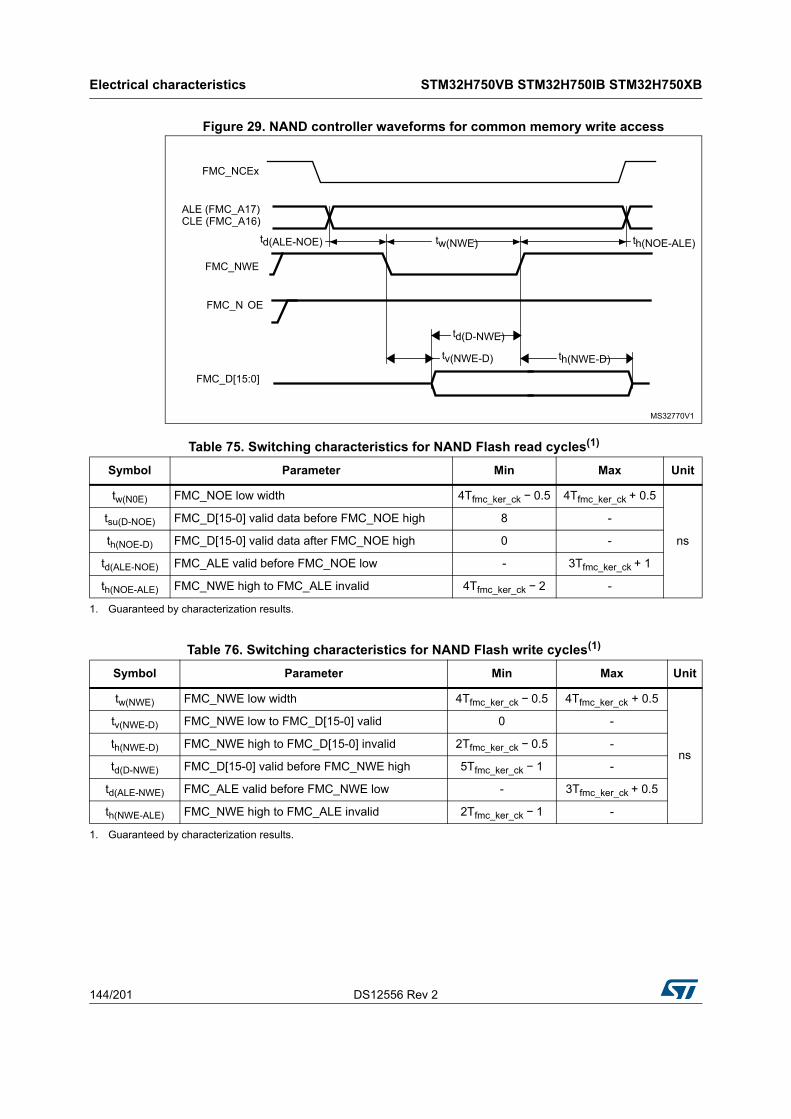
Electrical characteristics STM32H750VB STM32H750IB STM32H750XB
144/201 DS12556 Rev 2
Figure 29. NAND controller waveforms for common memory write access
MS32770V1
tw(NWE)
th(NWE-D)tv(NWE-D)
FMC_NWE
FMC_N OE
FMC_D[15:0]
td(D-NWE)
ALE (FMC_A17)CLE (FMC_A16)
FMC_NCEx
td(ALE-NOE) th(NOE-ALE)
Table 75. Switching characteristics for NAND Flash read cycles(1)
Symbol Parameter Min Max Unit
tw(N0E) FMC_NOE low width 4Tfmc_ker_ck − 0.5 4Tfmc_ker_ck + 0.5
ns
tsu(D-NOE) FMC_D[15-0] valid data before FMC_NOE high 8 -
th(NOE-D) FMC_D[15-0] valid data after FMC_NOE high 0 -
td(ALE-NOE) FMC_ALE valid before FMC_NOE low - 3Tfmc_ker_ck + 1
th(NOE-ALE) FMC_NWE high to FMC_ALE invalid 4Tfmc_ker_ck − 2 -
1. Guaranteed by characterization results.
Table 76. Switching characteristics for NAND Flash write cycles(1)
Symbol Parameter Min Max Unit
tw(NWE) FMC_NWE low width 4Tfmc_ker_ck − 0.5 4Tfmc_ker_ck + 0.5
ns
tv(NWE-D) FMC_NWE low to FMC_D[15-0] valid 0 -
th(NWE-D) FMC_NWE high to FMC_D[15-0] invalid 2Tfmc_ker_ck − 0.5 -
td(D-NWE) FMC_D[15-0] valid before FMC_NWE high 5Tfmc_ker_ck − 1 -
td(ALE-NWE) FMC_ALE valid before FMC_NWE low - 3Tfmc_ker_ck + 0.5
th(NWE-ALE) FMC_NWE high to FMC_ALE invalid 2Tfmc_ker_ck − 1 -
1. Guaranteed by characterization results.
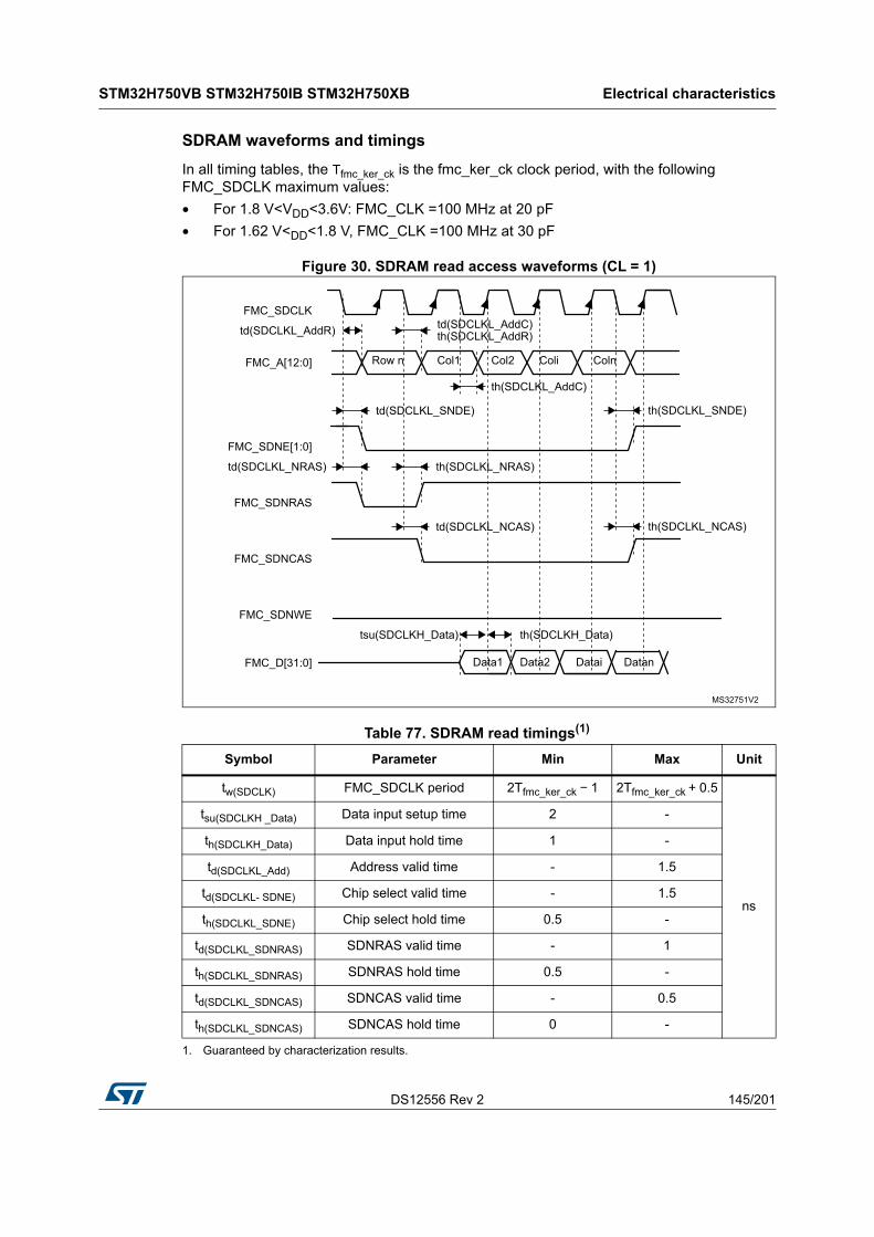
DS12556 Rev 2 145/201
STM32H750VB STM32H750IB STM32H750XB Electrical characteristics
189
SDRAM waveforms and timings
In all timing tables, the Tfmc_ker_ck is the fmc_ker_ck clock period, with the following FMC_SDCLK maximum values:
• For 1.8 V<VDD<3.6V: FMC_CLK =100 MHz at 20 pF
• For 1.62 V<DD<1.8 V, FMC_CLK =100 MHz at 30 pF
Figure 30. SDRAM read access waveforms (CL = 1)
Table 77. SDRAM read timings(1)
1. Guaranteed by characterization results.
Symbol Parameter Min Max Unit
tw(SDCLK) FMC_SDCLK period 2Tfmc_ker_ck − 1 2Tfmc_ker_ck + 0.5
ns
tsu(SDCLKH _Data) Data input setup time 2 -
th(SDCLKH_Data) Data input hold time 1 -
td(SDCLKL_Add) Address valid time - 1.5
td(SDCLKL- SDNE) Chip select valid time - 1.5
th(SDCLKL_SDNE) Chip select hold time 0.5 -
td(SDCLKL_SDNRAS) SDNRAS valid time - 1
th(SDCLKL_SDNRAS) SDNRAS hold time 0.5 -
td(SDCLKL_SDNCAS) SDNCAS valid time - 0.5
th(SDCLKL_SDNCAS) SDNCAS hold time 0 -
MS32751V2
Row n Col1
FMC_SDCLK
FMC_A[12:0]
FMC_SDNRAS
FMC_SDNCAS
FMC_SDNWE
FMC_D[31:0]
FMC_SDNE[1:0]
td(SDCLKL_AddR) td(SDCLKL_AddC)th(SDCLKL_AddR)
th(SDCLKL_AddC)
td(SDCLKL_SNDE)
tsu(SDCLKH_Data) th(SDCLKH_Data)
Col2 Coli Coln
Data2 Datai DatanData1
th(SDCLKL_SNDE)
td(SDCLKL_NRAS)
td(SDCLKL_NCAS) th(SDCLKL_NCAS)
th(SDCLKL_NRAS)
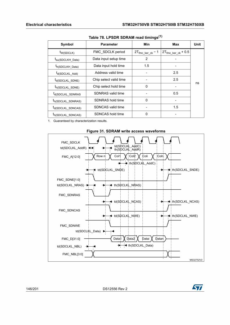
Electrical characteristics STM32H750VB STM32H750IB STM32H750XB
146/201 DS12556 Rev 2
Figure 31. SDRAM write access waveforms
Table 78. LPSDR SDRAM read timings(1)
1. Guaranteed by characterization results.
Symbol Parameter Min Max Unit
tW(SDCLK) FMC_SDCLK period 2Tfmc_ker_ck − 1 2Tfmc_ker_ck + 0.5
ns
tsu(SDCLKH_Data) Data input setup time 2 -
th(SDCLKH_Data) Data input hold time 1.5 -
td(SDCLKL_Add) Address valid time - 2.5
td(SDCLKL_SDNE) Chip select valid time - 2.5
th(SDCLKL_SDNE) Chip select hold time 0 -
td(SDCLKL_SDNRAS SDNRAS valid time - 0.5
th(SDCLKL_SDNRAS) SDNRAS hold time 0 -
td(SDCLKL_SDNCAS) SDNCAS valid time - 1.5
th(SDCLKL_SDNCAS) SDNCAS hold time 0 -
MS32752V2
Row n Col1
FMC_SDCLK
FMC_A[12:0]
FMC_SDNRAS
FMC_SDNCAS
FMC_SDNWE
FMC_D[31:0]
FMC_SDNE[1:0]
td(SDCLKL_AddR) td(SDCLKL_AddC)th(SDCLKL_AddR)
th(SDCLKL_AddC)
td(SDCLKL_SNDE)
td(SDCLKL_Data)
th(SDCLKL_Data)
Col2 Coli Coln
Data2 Datai DatanData1
th(SDCLKL_SNDE)
td(SDCLKL_NRAS)
td(SDCLKL_NCAS) th(SDCLKL_NCAS)
th(SDCLKL_NRAS)
td(SDCLKL_NWE) th(SDCLKL_NWE)
FMC_NBL[3:0]
td(SDCLKL_NBL)
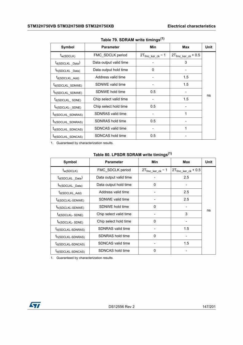
DS12556 Rev 2 147/201
STM32H750VB STM32H750IB STM32H750XB Electrical characteristics
189
Table 79. SDRAM write timings(1)
1. Guaranteed by characterization results.
Symbol Parameter Min Max Unit
tw(SDCLK) FMC_SDCLK period 2Tfmc_ker_ck − 1 2Tfmc_ker_ck + 0.5
ns
td(SDCLKL _Data) Data output valid time - 3
th(SDCLKL _Data) Data output hold time 0 -
td(SDCLKL_Add) Address valid time - 1.5
td(SDCLKL_SDNWE) SDNWE valid time - 1.5
th(SDCLKL_SDNWE) SDNWE hold time 0.5 -
td(SDCLKL_ SDNE) Chip select valid time - 1.5
th(SDCLKL-_SDNE) Chip select hold time 0.5 -
td(SDCLKL_SDNRAS) SDNRAS valid time - 1
th(SDCLKL_SDNRAS) SDNRAS hold time 0.5 -
td(SDCLKL_SDNCAS) SDNCAS valid time - 1
td(SDCLKL_SDNCAS) SDNCAS hold time 0.5 -
Table 80. LPSDR SDRAM write timings(1)
1. Guaranteed by characterization results.
Symbol Parameter Min Max Unit
tw(SDCLK) FMC_SDCLK period 2Tfmc_ker_ck − 1 2Tfmc_ker_ck + 0.5
ns
td(SDCLKL _Data) Data output valid time - 2.5
th(SDCLKL _Data) Data output hold time 0 -
td(SDCLKL_Add) Address valid time - 2.5
td(SDCLKL-SDNWE) SDNWE valid time - 2.5
th(SDCLKL-SDNWE) SDNWE hold time 0 -
td(SDCLKL- SDNE) Chip select valid time - 3
th(SDCLKL- SDNE) Chip select hold time 0 -
td(SDCLKL-SDNRAS) SDNRAS valid time - 1.5
th(SDCLKL-SDNRAS) SDNRAS hold time 0 -
td(SDCLKL-SDNCAS) SDNCAS valid time - 1.5
td(SDCLKL-SDNCAS) SDNCAS hold time 0 -
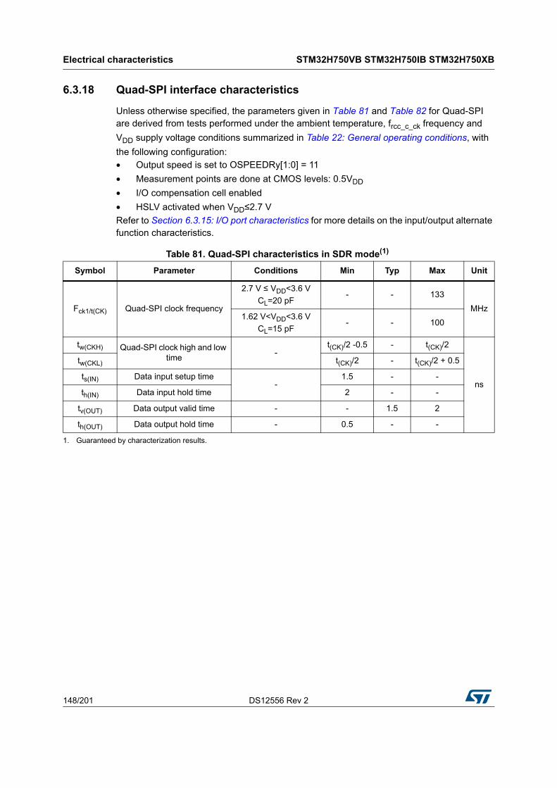
Electrical characteristics STM32H750VB STM32H750IB STM32H750XB
148/201 DS12556 Rev 2
6.3.18 Quad-SPI interface characteristics
Unless otherwise specified, the parameters given in Table 81 and Table 82 for Quad-SPI are derived from tests performed under the ambient temperature, frcc_c_ck frequency and
VDD supply voltage conditions summarized in Table 22: General operating conditions, with
the following configuration:• Output speed is set to OSPEEDRy[1:0] = 11
• Measurement points are done at CMOS levels: 0.5VDD
• I/O compensation cell enabled
• HSLV activated when VDD≤2.7 V
Refer to Section 6.3.15: I/O port characteristics for more details on the input/output alternate function characteristics.
Table 81. Quad-SPI characteristics in SDR mode(1)
Symbol Parameter Conditions Min Typ Max Unit
Fck1/t(CK) Quad-SPI clock frequency
2.7 V ≤ VDD<3.6 V
CL=20 pF- - 133
MHz1.62 V<VDD<3.6 V
CL=15 pF- - 100
tw(CKH) Quad-SPI clock high and low time
-t(CK)/2 -0.5 - t(CK)/2
ns
tw(CKL) t(CK)/2 - t(CK)/2 + 0.5
ts(IN) Data input setup time-
1.5 - -
th(IN) Data input hold time 2 - -
tv(OUT) Data output valid time - - 1.5 2
th(OUT) Data output hold time - 0.5 - -
1. Guaranteed by characterization results.
DS12556 Rev 2 149/201
STM32H750VB STM32H750IB STM32H750XB Electrical characteristics
189
Figure 32. Quad-SPI timing diagram - SDR mode
Figure 33. Quad-SPI timing diagram - DDR mode
Table 82. Quad SPI characteristics in DDR mode(1)
Symbol Parameter Conditions Min Typ Max Unit
Fck1/t(CK)Quad-SPI clock
frequency
2.7 V<VDD<3.6 V
CL=20 pF- - 100
MHz1.62 V<VDD<3.6 V
CL=15 pF- - 100
tw(CKH) Quad-SPI clock high and low time
-t(CK)/2 - 0.5 - t(CK)/2
ns
tw(CKL) t(CK)/2 - t(CK)/2+0.5
tsr(IN), tsf(IN) Data input setup time - 2 - -
thr(IN), thf(IN) Data input hold time - 2 - -
tvr(OUT), tvf(OUT)
Data output valid time
DHHC=0 - 3.5 4
DHHC=1
Pres=1, 2...- t(CK)/4+3.5 t(CK)/4+4
thr(OUT), thf(OUT)
Data output hold time
DHHC=0 3 - -
DHHC=1
Pres=1, 2...t(CK)/4+3 - -
1. Guaranteed by characterization results.
MSv36878V1
Data output D0 D1 D2
Clock
Data input D0 D1 D2
t(CK) tw(CKH) tw(CKL)tr(CK) tf(CK)
ts(IN) th(IN)
tv(OUT) th(OUT)
MSv36879V1
Data output D0 D2 D4
Clock
Data input D0 D2 D4
t(CK) tw(CKH) tw(CKL)tr(CK) tf(CK)
tsf(IN) thf(IN)
tvf(OUT) thr(OUT)
D1 D3 D5
D1 D3 D5
tvr(OUT) thf(OUT)
tsr(IN) thr(IN)
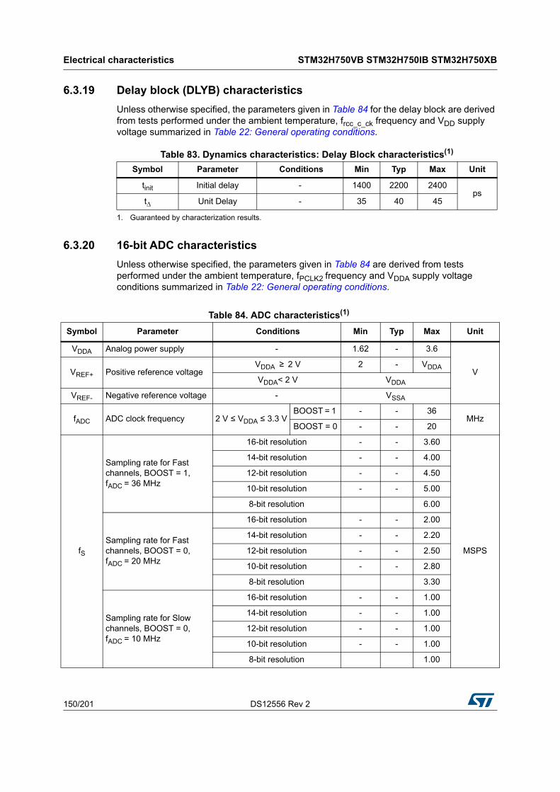
Electrical characteristics STM32H750VB STM32H750IB STM32H750XB
150/201 DS12556 Rev 2
6.3.19 Delay block (DLYB) characteristics
Unless otherwise specified, the parameters given in Table 84 for the delay block are derived from tests performed under the ambient temperature, frcc_c_ck frequency and VDD supply voltage summarized in Table 22: General operating conditions.
6.3.20 16-bit ADC characteristics
Unless otherwise specified, the parameters given in Table 84 are derived from tests performed under the ambient temperature, fPCLK2 frequency and VDDA supply voltage conditions summarized in Table 22: General operating conditions.
Table 83. Dynamics characteristics: Delay Block characteristics(1)
1. Guaranteed by characterization results.
Symbol Parameter Conditions Min Typ Max Unit
tinit Initial delay - 1400 2200 2400ps
t∆ Unit Delay - 35 40 45
Table 84. ADC characteristics(1)
Symbol Parameter Conditions Min Typ Max Unit
VDDA Analog power supply - 1.62 - 3.6
VVREF+ Positive reference voltage VDDA ≥ 2 V 2 - VDDA
VDDA< 2 V VDDA
VREF- Negative reference voltage - VSSA
fADC ADC clock frequency 2 V ≤ VDDA ≤ 3.3 VBOOST = 1 - - 36
MHzBOOST = 0 - - 20
fS
Sampling rate for Fast channels, BOOST = 1, fADC = 36 MHz
16-bit resolution - - 3.60
MSPS
14-bit resolution - - 4.00
12-bit resolution - - 4.50
10-bit resolution - - 5.00
8-bit resolution 6.00
Sampling rate for Fast channels, BOOST = 0, fADC = 20 MHz
16-bit resolution - - 2.00
14-bit resolution - - 2.20
12-bit resolution - - 2.50
10-bit resolution - - 2.80
8-bit resolution 3.30
Sampling rate for Slow channels, BOOST = 0, fADC = 10 MHz
16-bit resolution - - 1.00
14-bit resolution - - 1.00
12-bit resolution - - 1.00
10-bit resolution - - 1.00
8-bit resolution 1.00

DS12556 Rev 2 151/201
STM32H750VB STM32H750IB STM32H750XB Electrical characteristics
189
fTRIG External trigger frequencyfADC = 36 MHz - - 3.6 MHz
16-bit resolution - - 10 1/fADC
VAIN(2) Conversion voltage range - 0 - VREF+
VVCMIV
Common mode input voltage
-VREF/2−
10%VREF/2
VREF/2+10%
RAIN External input impedance - - - 50
CADCInternal sample and hold capacitor
- - 4 - pF
tADCREG_
STUPADC LDO startup time - - 5 10 µs
tSTAB ADC power-up time LDO already started 1conversion
cycle
tCALOffset and linearity calibration time
- 16384
1/fADC
tOFF_CAL Offset calibration time - 1280
tLATR
Trigger conversion latency for regular and injected channels without aborting the conversion
CKMODE = 00 1.5 2 2.5
CKMODE = 01 - - 2
CKMODE = 10 2.25
CKMODE = 11 2.125
tLATRINJ
Trigger conversion latency for regular and injected channels when a regular conversion is aborted
CKMODE = 00 2.5 3 3.5
CKMODE = 01 - - 3
CKMODE = 10 - - 3.25
CKMODE = 11 - - 3.125
tS Sampling time - 1.5 - 640.5
tCONVTotal conversion time (including sampling time)
N-bit resolutiontS + 0.5 + N/2
(9 to 648 cycles in 14-bit mode)
1. Guaranteed by design.
2. Depending on the package, VREF+ can be internally connected to VDDA and VREF- to VSSA.
Table 84. ADC characteristics(1) (continued)
Symbol Parameter Conditions Min Typ Max Unit

Electrical characteristics STM32H750VB STM32H750IB STM32H750XB
152/201 DS12556 Rev 2
Note: ADC accuracy vs. negative injection current: injecting a negative current on any analog input pins should be avoided as this significantly reduces the accuracy of the conversion
Table 85. ADC accuracy(1)(2)(3)
1. Guaranteed by characterization for BGA packages, the values for LQFP packages might differ.
2. ADC DC accuracy values are measured after internal calibration.
3. The above table gives the ADC performance in 16-bit mode.
Symbol Parameter Conditions(4)
4. ADC clock frequency ≤ 36 MHz, 2 V ≤ VDDA ≤3.3 V, 1.6 V ≤ VREF ≤ VDDA, BOOSTEN (for I/O) = 1.
Min Typ Max Unit
ETTotal
unadjusted error
Single ended
BOOST = 1 - ±6 -
±LSB
BOOST = 0 - ±8 -
DifferentialBOOST = 1 - ±10 -
BOOST = 0 - ±16 -
EDDifferential
linearity error
Single ended
BOOST = 1 - 2 -
BOOST = 0 - 1 -
DifferentialBOOST = 1 - 8 -
BOOST = 0 - 2 -
ELIntegral linearity
error
Single ended
BOOST = 1 - ±6 -
BOOST = 0 - ±4 -
DifferentialBOOST = 1 - ±6 -
BOOST = 0 - ±4 -
ENOB(5)
5. ENOB, SINAD, SNR and THD are specified for VDDA = VREF = 3.3 V.
Effective number of
bits
(2 MSPS)
Single ended
BOOST = 1 - 11.6 -
bitsBOOST = 0 - 12 -
DifferentialBOOST = 1 - 13.3 -
BOOST = 0 - 13.5 -
SINAD(5)
Signal-to-noise and distortion
ratio
(2 MSPS)
Single ended
BOOST = 1 - 71.6 -
dB
BOOST = 0 - 74 -
DifferentialBOOST = 1 - 81.83 -
BOOST = 0 - 83 -
SNR(5)Signal-to-noise ratio
(2 MSPS)
Single ended
BOOST = 1 - 72 -
BOOST = 0 - 74 -
DifferentialBOOST = 1 - 82 -
BOOST = 0 - 83 -
THD(5)Total
harmonic distortion
Single ended
BOOST = 1 - −78 -
BOOST = 0 - −80 -
DifferentialBOOST = 1 - −90 -
BOOST = 0 - −95 -
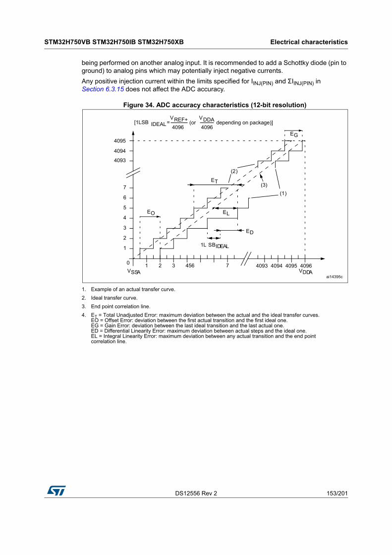
DS12556 Rev 2 153/201
STM32H750VB STM32H750IB STM32H750XB Electrical characteristics
189
being performed on another analog input. It is recommended to add a Schottky diode (pin to ground) to analog pins which may potentially inject negative currents.
Any positive injection current within the limits specified for IINJ(PIN) and ΣIINJ(PIN) in Section 6.3.15 does not affect the ADC accuracy.
Figure 34. ADC accuracy characteristics (12-bit resolution)
1. Example of an actual transfer curve.
2. Ideal transfer curve.
3. End point correlation line.
4. ET = Total Unadjusted Error: maximum deviation between the actual and the ideal transfer curves. EO = Offset Error: deviation between the first actual transition and the first ideal one. EG = Gain Error: deviation between the last ideal transition and the last actual one. ED = Differential Linearity Error: maximum deviation between actual steps and the ideal one. EL = Integral Linearity Error: maximum deviation between any actual transition and the end point correlation line.
ai14395c
EO
EG
1L SBIDEAL
4095
4094
4093
5
4
3
2
1
0
7
6
1 2 3 456 7 4093 4094 4095 4096
(1)
(2)
ET
ED
EL
(3)
VDDAVSSA
VREF+4096
(or depending on package)]VDDA4096
[1LSB IDEAL =

Electrical characteristics STM32H750VB STM32H750IB STM32H750XB
154/201 DS12556 Rev 2
Figure 35. Typical connection diagram using the ADC
1. Refer to Table 84 for the values of RAIN, RADC and CADC.
2. Cparasitic represents the capacitance of the PCB (dependent on soldering and PCB layout quality) plus the pad capacitance (roughly 5 pF). A high Cparasitic value downgrades conversion accuracy. To remedy this, fADC should be reduced.
ai17534b
STM32VDD
AINx
IL±1 μA0.6 VVT
RAIN(1)
CparasiticVAIN
0.6 VVT
RADC(1)
CADC(1)
12-bitconverter
Sample and hold ADC converter
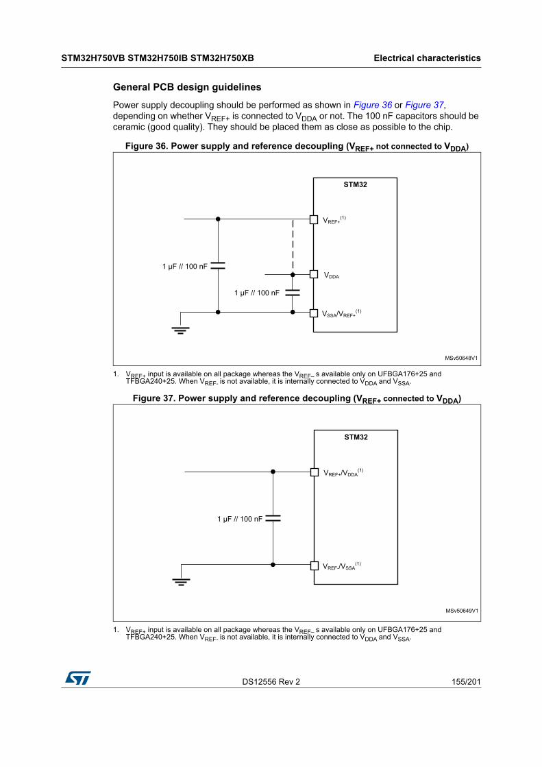
DS12556 Rev 2 155/201
STM32H750VB STM32H750IB STM32H750XB Electrical characteristics
189
General PCB design guidelines
Power supply decoupling should be performed as shown in Figure 36 or Figure 37, depending on whether VREF+ is connected to VDDA or not. The 100 nF capacitors should be ceramic (good quality). They should be placed them as close as possible to the chip.
Figure 36. Power supply and reference decoupling (VREF+ not connected to VDDA)
1. VREF+ input is available on all package whereas the VREF– s available only on UFBGA176+25 and TFBGA240+25. When VREF- is not available, it is internally connected to VDDA and VSSA.
Figure 37. Power supply and reference decoupling (VREF+ connected to VDDA)
1. VREF+ input is available on all package whereas the VREF– s available only on UFBGA176+25 and TFBGA240+25. When VREF- is not available, it is internally connected to VDDA and VSSA.
MSv50648V1
1 μF // 100 nF
1 μF // 100 nF
STM32
VREF+(1)
VSSA/VREF+(1)
VDDA
MSv50649V1
1 μF // 100 nF
STM32
VREF+/VDDA(1)
VREF-/VSSA(1)
Electrical characteristics STM32H750VB STM32H750IB STM32H750XB
156/201 DS12556 Rev 2
6.3.21 DAC electrical characteristics
Table 86. DAC characteristics(1)
Symbol Parameter Conditions Min Typ Max Unit
VDDA Analog supply voltage - 1.8 3.3 3.6
VVREF+ Positive reference voltage - 1.80 - VDDA
VREF-Negative reference voltage
- - VSSA -
RL Resistive LoadDAC output buffer ON
connected to VSSA
5 - -
connected to VDDA
25 - -
RO(2) Output Impedance DAC output buffer OFF 10.3 13 16
RBON
Output impedance sample and hold mode, output buffer ON
DAC output buffer ON
VDD = 2.7 V - - 1.6
VDD = 2.0 V - - 2.6
RBOFF
Output impedance sample and hold mode, output buffer OFF
DAC output buffer OFF
VDD = 2.7 V - - 17.8
VDD = 2.0 V - - 18.7
CL(2)
Capacitive LoadDAC output buffer OFF - - 50 pF
CSH(2) Sample and Hold mode - 0.1 1 µF
VDAC_OUTVoltage on DAC_OUT output
DAC output buffer ON 0.2 -VREF+ −0.2 V
DAC output buffer OFF 0 - VREF+
tSETTLING
Settling time (full scale: for a 12-bit code transition between the lowest and the highest input codes when DAC_OUT reaches the final value of ±0.5LSB, ±1LSB, ±2LSB, ±4LSB, ±8LSB)
Normal mode, DAC output buffer OFF, ±1LSB CL=10 pF
- 1.7(2) 2(2) µs
tWAKEUP(3)
Wakeup time from off state (setting the Enx bit in the DAC Control register) until the ±1LSB final value
Normal mode, DAC output buffer ON, CL ≤ 50 pF, RL = 5 - 5 7.5 µs
Voffset(2) Middle code offset for 1
trim code step
VREF+ = 3.6 V - 850 -µV
VREF+ = 1.8 V - 425 -

DS12556 Rev 2 157/201
STM32H750VB STM32H750IB STM32H750XB Electrical characteristics
189
IDDA(DAC)DAC quiescent
consumption from VDDA
DAC output buffer ON
No load, middle code (0x800)
- 360 -
µA
No load, worst code (0xF1C)
- 490 -
DAC output buffer OFF
No load, middle/worst code (0x800)
- 20 -
Sample and Hold mode, CSH=100 nF
-360*TON/
(TON+TOFF)-
IDDV(DAC)DAC consumption from VREF+
DAC output buffer ON
No load, middle code (0x800)
- 170 -
No load, worst code (0xF1C)
- 170 -
DAC output buffer OFF
No load, middle/worst code (0x800)
- 160 -
Sample and Hold mode, Buffer ON, CSH=100 nF (worst code)
-170*TON/
(TON+TOFF)-
Sample and Hold mode, Buffer OFF, CSH=100 nF (worst code)
-160*TON/
(TON+TOFF)-
1. Guaranteed by characterization results.
2. Guaranteed by design.
3. In buffered mode, the output can overshoot above the final value for low input code (starting from the minimum value).
Table 86. DAC characteristics(1) (continued)
Symbol Parameter Conditions Min Typ Max Unit
Table 87. DAC accuracy(1)
Symbol Parameter Conditions Min Typ Max Unit
DNLDifferential non
linearity(2)
DAC output buffer ON - ±2 -LSB
DAC output buffer OFF - ±2 -
INL Integral non linearity(3)
DAC output buffer ON, CL ≤ 50 pF, RL ≥ 5 - ±4 -
LSBDAC output buffer OFF,
CL ≤ 50 pF, no RL- ±4 -
OffsetOffset error at code
0x800 (3)
DAC output buffer ON,
CL ≤ 50 pF, RL ≥ 5
VREF+ = 3.6 V - - ±12
LSBVREF+ = 1.8 V - - ±25
DAC output buffer OFF, CL ≤ 50 pF, no RL
- - ±8
Offset1Offset error at code
0x001(4)DAC output buffer OFF,
CL ≤ 50 pF, no RL- - ±5 LSB
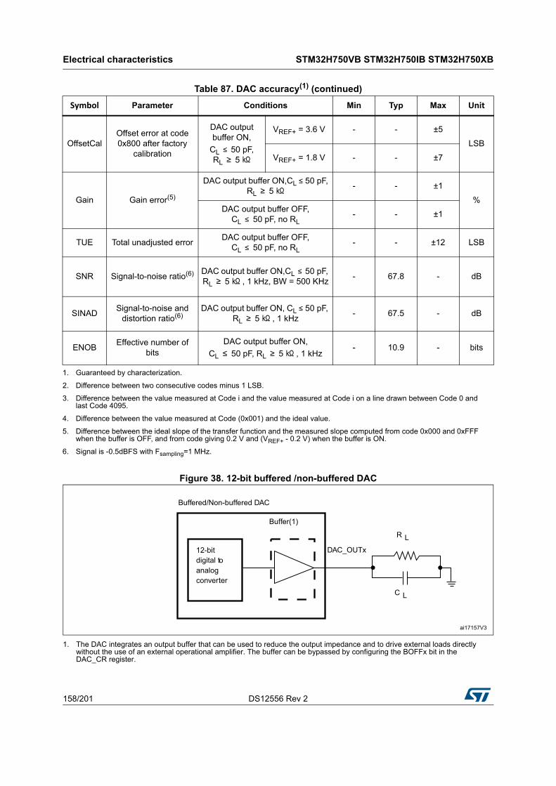
Electrical characteristics STM32H750VB STM32H750IB STM32H750XB
158/201 DS12556 Rev 2
Figure 38. 12-bit buffered /non-buffered DAC
1. The DAC integrates an output buffer that can be used to reduce the output impedance and to drive external loads directly without the use of an external operational amplifier. The buffer can be bypassed by configuring the BOFFx bit in the DAC_CR register.
OffsetCalOffset error at code 0x800 after factory
calibration
DAC output buffer ON,
CL ≤ 50 pF, RL ≥ 5
VREF+ = 3.6 V - - ±5
LSB
VREF+ = 1.8 V - - ±7
Gain Gain error(5)
DAC output buffer ON,CL ≤ 50 pF, RL ≥ 5 - - ±1
%DAC output buffer OFF,
CL ≤ 50 pF, no RL- - ±1
TUE Total unadjusted errorDAC output buffer OFF,
CL ≤ 50 pF, no RL- - ±12 LSB
SNR Signal-to-noise ratio(6) DAC output buffer ON,CL ≤ 50 pF, RL ≥ 5 , 1 kHz, BW = 500 KHz
- 67.8 - dB
SINADSignal-to-noise and
distortion ratio(6)DAC output buffer ON, CL ≤ 50 pF,
RL ≥ 5 , 1 kHz- 67.5 - dB
ENOBEffective number of
bitsDAC output buffer ON,
CL ≤ 50 pF, RL ≥ 5 , 1 kHz- 10.9 - bits
1. Guaranteed by characterization.
2. Difference between two consecutive codes minus 1 LSB.
3. Difference between the value measured at Code i and the value measured at Code i on a line drawn between Code 0 and last Code 4095.
4. Difference between the value measured at Code (0x001) and the ideal value.
5. Difference between the ideal slope of the transfer function and the measured slope computed from code 0x000 and 0xFFF when the buffer is OFF, and from code giving 0.2 V and (VREF+ - 0.2 V) when the buffer is ON.
6. Signal is -0.5dBFS with Fsampling=1 MHz.
Table 87. DAC accuracy(1) (continued)
Symbol Parameter Conditions Min Typ Max Unit
R L
C L
Buffered/Non-buffered DAC
DAC_OUTx
Buffer(1)
12-bit digital to analog converter
ai17157V3

DS12556 Rev 2 159/201
STM32H750VB STM32H750IB STM32H750XB Electrical characteristics
189
6.3.22 Voltage reference buffer characteristics
Table 88. VREFBUF characteristics(1)
Symbol Parameter Conditions Min Typ Max Unit
VDDA Analog supply voltage
Normal mode
VSCALE = 000 2.8 3.3 3.6
V
VSCALE = 001 2.4 - 3.6
VSCALE = 010 2.1 - 3.6
VSCALE = 011 1.8 - 3.6
Degraded mode
VSCALE = 000 1.62 - 2.80
VSCALE = 001 1.62 - 2.40
VSCALE = 010 1.62 - 2.10
VSCALE = 011 1.62 - 1.80
VREFBUF
_OUT
Voltage Reference Buffer Output
Normal mode
VSCALE = 000 - 2.5 -
VSCALE = 001 - 2.048 -
VSCALE = 010 - 1.8 -
VSCALE = 011 - 1.5 -
Degraded mode(2)
VSCALE = 000VDDA−150 mV
- VDDA
VSCALE = 001VDDA−150 mV
- VDDA
VSCALE = 010VDDA−150 mV
- VDDA
VSCALE = 011VDDA−150 mV
- VDDA
TRIM Trim step resolution - - - ±0.05 ±0.2 %
CL Load capacitor - - 0.5 1 1.50 uF
esrEquivalent Serial
Resistor of CL- - - - 2 Ω
Iload Static load current - - - - 4 mA
Iline_reg Line regulation 2.8 V ≤ VDDA ≤ 3.6 VIload = 500 µA - 200 -
ppm/VIload = 4 mA - 100 -
Iload_reg Load regulation 500 µA ≤ ILOAD ≤ 4 mA Normal Mode - 50 -ppm/mA
Tcoeff Temperature coefficient
−40 °C < TJ < +105 °C - - -Tcoeff
xVREFINT + 50 ppm/
°C
0 °C < TJ < +50 °C - - -Tcoeff
xVREFINT + 50
PSRR Power supply rejectionDC - - 60 -
dB100KHz - - 40 -

Electrical characteristics STM32H750VB STM32H750IB STM32H750XB
160/201 DS12556 Rev 2
6.3.23 Temperature sensor characteristics
tSTART Start-up time
CL=0.5 µF - - 300 -
µsCL=1 µF - - 500 -
CL=1.5 µF - - 650 -
IINRUSH
Control of maximum DC current drive on VREFBUF_OUT during
startup phase(3)
- - 8 - mA
IDDA(VRE
FBUF)
VREFBUF consumption from
VDDA
ILOAD = 0 µA - - 15 25
µAILOAD = 500 µA - - 16 30
ILOAD = 4 mA - - 32 50
1. Guaranteed by design.
2. In degraded mode, the voltage reference buffer cannot accurately maintain the output voltage (VDDA−drop voltage).
3. To properly control VREFBUF IINRUSH current during the startup phase and the change of scaling, VDDA voltage should be in the range of 1.8 V-3.6 V, 2.1 V-3.6 V, 2.4 V-3.6 V and 2.8 V-3.6 V for VSCALE = 011, 010, 001 and 000, respectively.
Table 88. VREFBUF characteristics(1) (continued)
Symbol Parameter Conditions Min Typ Max Unit
Table 89. Temperature sensor characteristics
Symbol Parameter Min Typ Max Unit
TL(1)
1. Guaranteed by design.
VSENSE linearity with temperature - - 3 °C
Avg_Slope(2)
2. Guaranteed by characterization.
Average slope - 2 - mV/°C
V30(3)
3. Measured at VDDA = 3.3 V ± 10 mV. The V30 ADC conversion result is stored in the TS_CAL1 byte.
Voltage at 30°C ± 5 °C - 0.62 - V
tstart_run(1) Startup time in Run mode (buffer startup) - - 25.2
µstS_temp
(1) ADC sampling time when reading the temperature 9 - -
Isens(1) Sensor consumption - 0.18 0.31
µAIsensbuf
(1) Sensor buffer consumption - 3.8 6.5
Table 90. Temperature sensor calibration values
Symbol Parameter Memory address
TS_CAL1Temperature sensor raw data acquired value at 30 °C, VDDA=3.3 V
0x1FF1 E820 -0x1FF1 E821
TS_CAL2Temperature sensor raw data acquired value at 110 °C, VDDA=3.3 V
0x1FF1 E840 - 0x1FF1 E841

DS12556 Rev 2 161/201
STM32H750VB STM32H750IB STM32H750XB Electrical characteristics
189
6.3.24 VBAT monitoring characteristics
6.3.25 Voltage booster for analog switch
Table 91. VBAT monitoring characteristics
Symbol Parameter Min Typ Max Unit
R Resistor bridge for VBAT - 26 - KΩ
Q Ratio on VBAT measurement - 4 - -
Er(1)
1. Guaranteed by design.
Error on Q –10 - +10 %
tS_vbat(1) ADC sampling time when reading VBAT input 9 - - µs
Table 92. VBAT charging characteristics
Symbol Parameter Condition Min Typ Max Unit
RBC Battery charging resistorVBRS in PWR_CR3= 0 - 5 -
KΩ VBRS in PWR_CR3= 1 1.5 -
Table 93. Voltage booster for analog switch characteristics(1)
1. Guaranteed by characterization results.
Symbol Parameter Condition Min Typ Max Unit
VDD Supply voltage - 1.62 2-6 3.6 V
tSU(BOOST) Booster startup time - - - 50 µs
IDD(BOOST) Booster consumption 1.62 V ≤ VDD ≤ 2.7 V - - 125
µA2.7 V < VDD < 3.6 V - - 250
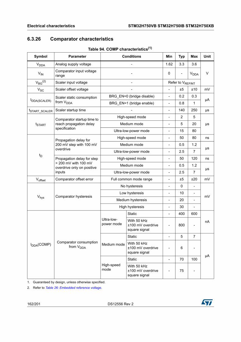
Electrical characteristics STM32H750VB STM32H750IB STM32H750XB
162/201 DS12556 Rev 2
6.3.26 Comparator characteristics
Table 94. COMP characteristics(1)
Symbol Parameter Conditions Min Typ Max Unit
VDDA Analog supply voltage - 1.62 3.3 3.6
VVINComparator input voltage range
- 0 - VDDA
VBG(2) Scaler input voltage - Refer to VREFINT
VSC Scaler offset voltage - - ±5 ±10 mV
IDDA(SCALER)Scaler static consumption from VDDA
BRG_EN=0 (bridge disable) - 0.2 0.3µA
BRG_EN=1 (bridge enable) - 0.8 1
tSTART_SCALER Scaler startup time - - 140 250 µs
tSTART
Comparator startup time to reach propagation delay specification
High-speed mode - 2 5
µsMedium mode - 5 20
Ultra-low-power mode - 15 80
tD
Propagation delay for 200 mV step with 100 mV overdrive
High-speed mode - 50 80 ns
Medium mode - 0.5 1.2µs
Ultra-low-power mode - 2.5 7
Propagation delay for step > 200 mV with 100 mV overdrive only on positive inputs
High-speed mode - 50 120 ns
Medium mode - 0.5 1.2µs
Ultra-low-power mode - 2.5 7
Voffset Comparator offset error Full common mode range - ±5 ±20 mV
Vhys Comparator hysteresis
No hysteresis - 0 -
mVLow hysteresis - 10 -
Medium hysteresis - 20 -
High hysteresis - 30 -
IDDA(COMP)Comparator consumption
from VDDA
Ultra-low-power mode
Static - 400 600
nAWith 50 kHz ±100 mV overdrive square signal
- 800 -
Medium mode
Static - 5 7
µA
With 50 kHz ±100 mV overdrive square signal
- 6 -
High-speed mode
Static - 70 100
With 50 kHz ±100 mV overdrive square signal
- 75 -
1. Guaranteed by design, unless otherwise specified.
2. Refer to Table 26: Embedded reference voltage.

DS12556 Rev 2 163/201
STM32H750VB STM32H750IB STM32H750XB Electrical characteristics
189
6.3.27 Operational amplifiers characteristics
Table 95. OPAMP characteristics(1)
Symbol Parameter Conditions Min Typ Max Unit
VDDAAnalog supply voltage Range
- 2 3.3 3.6
V
CMIRCommon Mode Input Range
- 0 - VDDA
VIOFFSET Input offset voltage
25°C, no load on output - - ±1.5
mVAll voltages and
temperature, no load- - ±2.5
ΔVIOFFSET Input offset voltage drift - - ±3.0 - μV/°C
TRIMOFFSETP
TRIMLPOFFSETP
Offset trim step at low common input voltage (0.1*VDDA)
- - 1.1 1.5
mV
TRIMOFFSETN
TRIMLPOFFSETN
Offset trim step at high common input voltage (0.9*VDDA)
- - 1.1 1.5
ILOAD Drive current - - - 500μA
ILOAD_PGA Drive current in PGA mode - - - 270
CLOAD Capacitive load - - - 50 pF
CMRRCommon mode rejection ratio
- - 80 - dB
PSRRPower supply rejection ratio
CLOAD ≤ 50pf / RLOAD ≥ 4 kΩ(2) at 1 kHz,
Vcom=VDDA/250 66 - dB
GBWGain bandwidth for high supply range
- 4 7.3 12.3 MHz
SRSlew rate (from 10% and 90% of output voltage)
Normal mode - 3 -V/µs
High-speed mode - 30 -
AO Open loop gain - 59 90 129 dB
φm Phase margin - - 55 - °
GM Gain margin - - 12 - dB
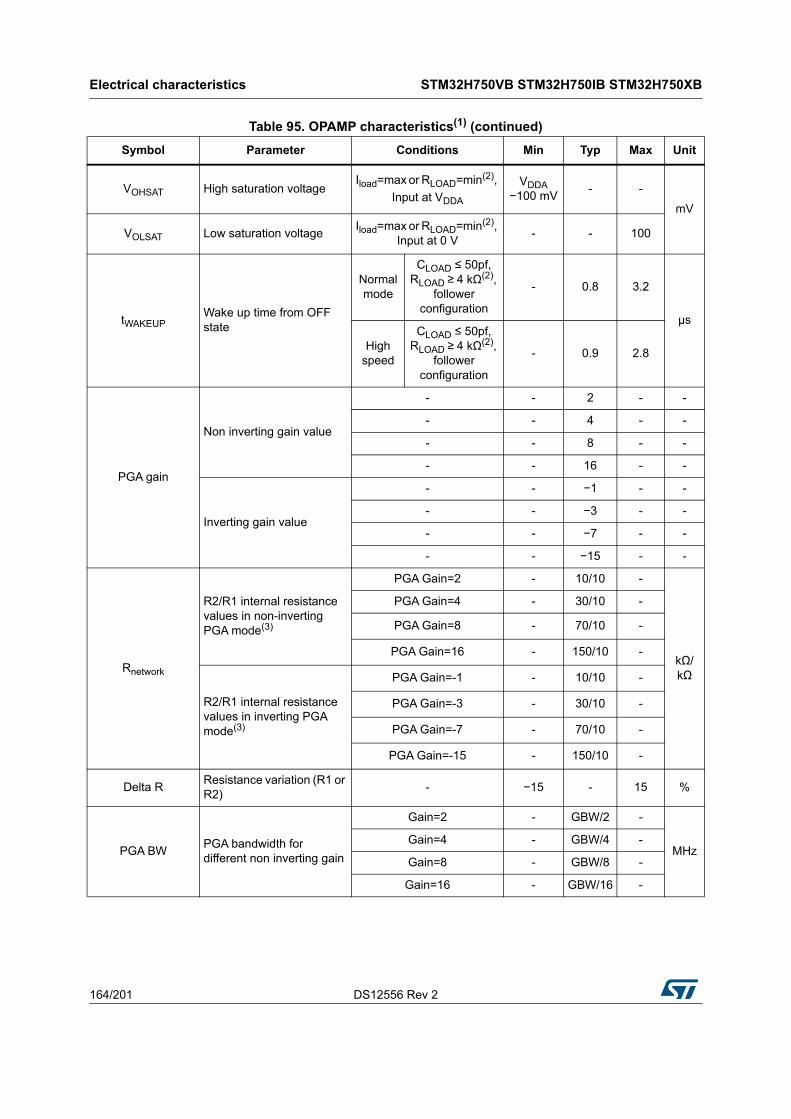
Electrical characteristics STM32H750VB STM32H750IB STM32H750XB
164/201 DS12556 Rev 2
VOHSAT High saturation voltageIload=max or RLOAD=min(2),
Input at VDDA
VDDA −100 mV
- -
mV
VOLSAT Low saturation voltageIload=max or RLOAD=min(2),
Input at 0 V- - 100
tWAKEUPWake up time from OFF state
Normal mode
CLOAD ≤ 50pf, RLOAD ≥ 4 kΩ(2),
follower configuration
- 0.8 3.2
µs
High speed
CLOAD ≤ 50pf, RLOAD ≥ 4 kΩ(2),
follower configuration
- 0.9 2.8
PGA gain
Non inverting gain value
- - 2 - -
- - 4 - -
- - 8 - -
- - 16 - -
Inverting gain value
- - −1 - -
- - −3 - -
- - −7 - -
- - −15 - -
Rnetwork
R2/R1 internal resistance values in non-inverting PGA mode(3)
PGA Gain=2 - 10/10 -
kΩ/kΩ
PGA Gain=4 - 30/10 -
PGA Gain=8 - 70/10 -
PGA Gain=16 - 150/10 -
R2/R1 internal resistance values in inverting PGA mode(3)
PGA Gain=-1 - 10/10 -
PGA Gain=-3 - 30/10 -
PGA Gain=-7 - 70/10 -
PGA Gain=-15 - 150/10 -
Delta RResistance variation (R1 or R2)
- −15 - 15 %
PGA BWPGA bandwidth for different non inverting gain
Gain=2 - GBW/2 -
MHzGain=4 - GBW/4 -
Gain=8 - GBW/8 -
Gain=16 - GBW/16 -
Table 95. OPAMP characteristics(1) (continued)
Symbol Parameter Conditions Min Typ Max Unit

DS12556 Rev 2 165/201
STM32H750VB STM32H750IB STM32H750XB Electrical characteristics
189
en Voltage noise density
at 1 KHz output loaded
with 4 kΩ
- 140 -nV/√Hzat
10 KHz- 55 -
IDDA(OPAMP)OPAMP consumption from VDDA
Normal mode no Load,
quiescent mode, follower
- 570 1000
µAHigh-speed mode
- 610 1200
1. Guaranteed by design, unless otherwise specified.
2. RLOAD is the resistive load connected to VSSA or to VDDA.
3. R2 is the internal resistance between the OPAMP output and th OPAMP inverting input. R1 is the internal resistance between the OPAMP inverting input and ground. PGA gain = 1 + R2/R1.
Table 95. OPAMP characteristics(1) (continued)
Symbol Parameter Conditions Min Typ Max Unit

Electrical characteristics STM32H750VB STM32H750IB STM32H750XB
166/201 DS12556 Rev 2
6.3.28 Digital filter for Sigma-Delta Modulators (DFSDM) characteristics
Unless otherwise specified, the parameters given in Table 96 for DFSDM are derived from tests performed under the ambient temperature, fPCLKx frequency and VDD supply voltage summarized in Table 22: General operating conditions, with the following configuration:
• Output speed is set to OSPEEDRy[1:0] = 10
• Capacitive load C = 30 pF
• Measurement points are done at CMOS levels: 0.5VDD
Refer to Section 6.3.15: I/O port characteristics for more details on the input/output alternate function characteristics (DFSDMx_CKINx, DFSDMx_DATINx, DFSDMx_CKOUT for DFSDMx).
Table 96. DFSDM measured timing 1.62-3.6 V(1)
Symbol Parameter Conditions Min Typ Max Unit
fDFSDMCLK DFSDM clock 1.62 V < VDD < 3.6 V - - fSYSCLK
MHz
fCKIN(1/TCKIN)
Input clock frequency
SPI mode (SITP[1:0]=0,1),External clock mode (SPICKSEL[1:0]=0),1.62 V < VDD < 3.6 V
- -20
(fDFSDMCLK/4)
SPI mode (SITP[1:0]=0,1),External clock mode (SPICKSEL[1:0]=0),2.7 < VDD < 3.6 V
- -20
(fDFSDMCLK/4)
SPI mode (SITP[1:0]=0,1),Internal clock mode (SPICKSEL[1:0]≠0),1.62 < VDD < 3.6 V
- -20
(fDFSDMCLK/4)
SPI mode (SITP[1:0]=0,1),Internal clock mode (SPICKSEL[1:0]≠0),
2.7 < VDD < 3.6 V
- -20
(fDFSDMCLK/4)
fCKOUTOutput clock
frequency1.62 < VDD < 3.6 V - - 20
DuCyCKOUT
Output clock frequency duty
cycle1.62 < VDD < 3.6 V 45 50 55 %
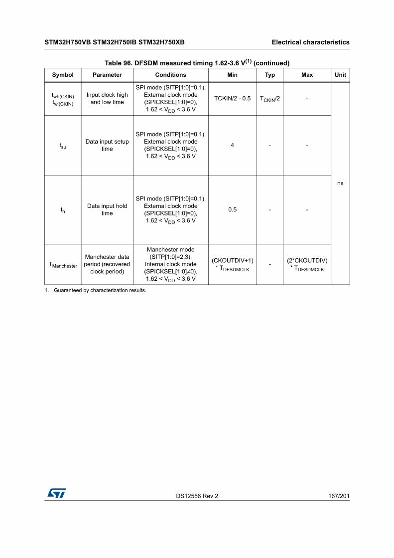
DS12556 Rev 2 167/201
STM32H750VB STM32H750IB STM32H750XB Electrical characteristics
189
twh(CKIN)twl(CKIN)
Input clock high and low time
SPI mode (SITP[1:0]=0,1),External clock mode (SPICKSEL[1:0]=0),1.62 < VDD < 3.6 V
TCKIN/2 - 0.5 TCKIN/2 -
ns
tsuData input setup
time
SPI mode (SITP[1:0]=0,1),External clock mode (SPICKSEL[1:0]=0),1.62 < VDD < 3.6 V
4 - -
thData input hold
time
SPI mode (SITP[1:0]=0,1),External clock mode (SPICKSEL[1:0]=0),1.62 < VDD < 3.6 V
0.5 - -
TManchester
Manchester data period (recovered
clock period)
Manchester mode (SITP[1:0]=2,3),
Internal clock mode (SPICKSEL[1:0]≠0),1.62 < VDD < 3.6 V
(CKOUTDIV+1) * TDFSDMCLK
-(2*CKOUTDIV)
* TDFSDMCLK
1. Guaranteed by characterization results.
Table 96. DFSDM measured timing 1.62-3.6 V(1) (continued)
Symbol Parameter Conditions Min Typ Max Unit
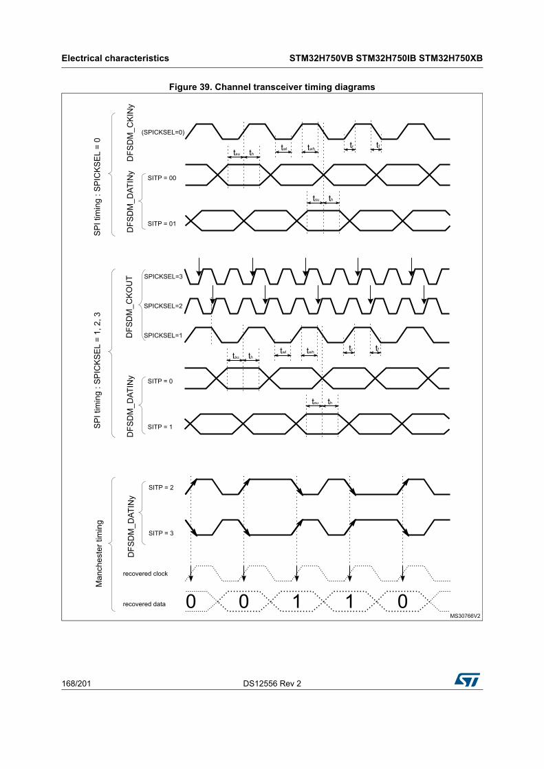
Electrical characteristics STM32H750VB STM32H750IB STM32H750XB
168/201 DS12556 Rev 2
Figure 39. Channel transceiver timing diagrams
MS30766V2
SITP = 0
DFS
DM
_CK
OU
TD
FSD
M_D
ATIN
y
SITP = 1
tsu th
tsu th
tftrtwl twh
SP
I tim
ing
: SP
ICK
SE
L =
1, 2
, 3
recovered clock
SITP = 2
DFS
DM
_DAT
INy
SITP = 3
Man
ches
ter t
imin
g
recovered data 1 1 000
SITP = 00
DFS
DM
_CK
INy
DFS
DM
_DAT
INy
SITP = 01
tsu th
tsu th
tftrtwl twh
SP
I tim
ing
: SP
ICK
SE
L =
0
SPICKSEL=2
SPICKSEL=1
(SPICKSEL=0)
SPICKSEL=3

DS12556 Rev 2 169/201
STM32H750VB STM32H750IB STM32H750XB Electrical characteristics
189
6.3.29 Camera interface (DCMI) timing specifications
Unless otherwise specified, the parameters given in Table 97 for DCMI are derived from tests performed under the ambient temperature, frcc_c_ck frequency and VDD supply voltage summarized in Table 22: General operating conditions, with the following configuration:
• DCMI_PIXCLK polarity: falling
• DCMI_VSYNC and DCMI_HSYNC polarity: high
• Data formats: 14 bits
• Capacitive load C=30 pF
• Measurement points are done at CMOS levels: 0.5VDD
Figure 40. DCMI timing diagram
Table 97. DCMI characteristics(1)
1. Guaranteed by characterization results.
Symbol Parameter Min Max Unit
- Frequency ratio DCMI_PIXCLK/frcc_c_ck - 0.4 -
DCMI_PIXCLK Pixel clock input - 80 MHz
DPixel Pixel clock input duty cycle 30 70 %
tsu(DATA) Data input setup time 1 -
ns
th(DATA) Data input hold time 1 -
tsu(HSYNC)
tsu(VSYNC)DCMI_HSYNC/DCMI_VSYNC input setup time 1.5 -
th(HSYNC)
th(VSYNC)DCMI_HSYNC/DCMI_VSYNC input hold time 1 -
MS32414V2
DCMI_PIXCLK
tsu(VSYNC)
tsu(HSYNC)
DCMI_HSYNC
DCMI_VSYNC
DATA[0:13]
1/DCMI_PIXCLK
th(HSYNC)
th(HSYNC)
tsu(DATA) th(DATA)
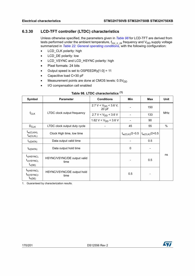
Electrical characteristics STM32H750VB STM32H750IB STM32H750XB
170/201 DS12556 Rev 2
6.3.30 LCD-TFT controller (LTDC) characteristics
Unless otherwise specified, the parameters given in Table 98 for LCD-TFT are derived from tests performed under the ambient temperature, frcc_c_ck frequency and VDD supply voltage summarized in Table 22: General operating conditions, with the following configuration:
• LCD_CLK polarity: high
• LCD_DE polarity: low
• LCD_VSYNC and LCD_HSYNC polarity: high
• Pixel formats: 24 bits
• Output speed is set to OSPEEDRy[1:0] = 11
• Capacitive load C=30 pF
• Measurement points are done at CMOS levels: 0.5VDD
• I/O compensation cell enabled
Table 98. LTDC characteristics (1)
Symbol Parameter Conditions Min Max Unit
fCLK LTDC clock output frequency
2.7 V < VDD < 3.6 V, 20 pF
- 150
MHz2.7 V < VDD < 3.6 V - 133
1.62 V < VDD < 3.6 V - 90
DCLK LTDC clock output duty cycle - 45 55 %
tw(CLKH),tw(CLKL)
Clock High time, low time tw(CLK)/2−0.5 tw(CLK)/2+0.5
ns
tv(DATA) Data output valid time - 0.5
th(DATA) Data output hold time 0 -
tv(HSYNC),
tv(VSYNC),
tv(DE)
HSYNC/VSYNC/DE output valid time
- 0.5
th(HSYNC),
th(VSYNC),th(DE)
HSYNC/VSYNC/DE output hold time
0.5 -
1. Guaranteed by characterization results.
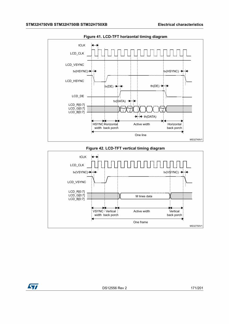
DS12556 Rev 2 171/201
STM32H750VB STM32H750IB STM32H750XB Electrical characteristics
189
Figure 41. LCD-TFT horizontal timing diagram
Figure 42. LCD-TFT vertical timing diagram
MS32749V1
LCD_CLK
tv(HSYNC)
LCD_HSYNC
LCD_DE
LCD_R[0:7]LCD_G[0:7]LCD_B[0:7]
tCLK
LCD_VSYNC
tv(HSYNC)
tv(DE) th(DE)
Pixel1
Pixel2
tv(DATA)
th(DATA)
PixelN
HSYNCwidth
Horizontalback porch
Active width Horizontalback porch
One line
MS32750V1
LCD_CLK
tv(VSYNC)
LCD_R[0:7]LCD_G[0:7]LCD_B[0:7]
tCLK
LCD_VSYNC
tv(VSYNC)
M lines data
VSYNCwidth
Verticalback porch
Active width Verticalback porch
One frame
Electrical characteristics STM32H750VB STM32H750IB STM32H750XB
172/201 DS12556 Rev 2
6.3.31 Timer characteristics
The parameters given in Table 99 are guaranteed by design.
Refer to Section 6.3.15: I/O port characteristics for details on the input/output alternate function characteristics (output compare, input capture, external clock, PWM output).
Table 99. TIMx characteristics(1)(2)
1. TIMx is used as a general term to refer to the TIM1 to TIM17 timers.
2. Guaranteed by design.
Symbol Parameter Conditions(3)
3. The maximum timer frequency on APB1 or APB2 is up to 200 MHz, by setting the TIMPRE bit in the RCC_CFGR register, if APBx prescaler is 1 or 2 or 4, then TIMxCLK = rcc_hclk1, otherwise TIMxCLK = 4x Frcc_pclkx_d2.
Min Max Unit
tres(TIM) Timer resolution time
AHB/APBx prescaler=1 or 2 or 4, fTIMxCLK =
200 MHz1 - tTIMxCLK
AHB/APBx prescaler>4, fTIMxCLK =
100 MHz1 - tTIMxCLK
fEXTTimer external clock frequency on CH1 to CH4 fTIMxCLK = 200 MHz
0 fTIMxCLK/2 MHz
ResTIM Timer resolution - 16/32 bit
tMAX_COUNTMaximum possible count with 32-bit counter
- -65536 × 65536
tTIMxCLK

DS12556 Rev 2 173/201
STM32H750VB STM32H750IB STM32H750XB Electrical characteristics
189
6.3.32 Communications interfaces
I2C interface characteristics
The I2C interface meets the timings requirements of the I2C-bus specification and user manual rev. 03 for:
• Standard-mode (Sm): with a bit rate up to 100 kbit/s
• Fast-mode (Fm): with a bit rate up to 400 kbit/s.
• Fast-mode Plus (Fm+): with a bit rate up to 1Mbit/s.
The I2C timings requirements are guaranteed by design when the I2C peripheral is properly configured (refer to RM0433 reference manual) and when the i2c_ker_ck frequency is greater than the minimum shown in the table below:
The SDA and SCL I/O requirements are met with the following restrictions:
• The SDA and SCL I/O pins are not “true” open-drain. When configured as open-drain, the PMOS connected between the I/O pin and VDD is disabled, but is still present.
• The 20 mA output drive requirement in Fast-mode Plus is not supported. This limits the maximum load Cload supported in Fm+, which is given by these formulas:
tr(SDA/SCL)=0.8473xRpxCload
Rp(min)= (VDD-VOL(max))/IOL(max)
Where Rp is the I2C lines pull-up. Refer to Section 6.3.15: I/O port characteristics for the I2C I/Os characteristics.
All I2C SDA and SCL I/Os embed an analog filter. Refer to Table 101 for the analog filter characteristics:
Table 100. Minimum i2c_ker_ck frequency in all I2C modes
Symbol Parameter Condition Min Unit
f(I2CCLK)I2CCLK
frequency
Standard-mode 2
MHz
Fast-mode
Analog filter ON
DNF=08
Analog filter OFF
DNF=19
Fast-mode Plus
Analog filter ON
DNF=017
Analog filter OFF
DNF=116
Table 101. I2C analog filter characteristics(1)
1. Guaranteed by design.
Symbol Parameter Min Max Unit
tAFMaximum pulse width of spikes that are suppressed by the analog filter
50(2)
2. Spikes with widths below tAF(min) are filtered.
260(3)
3. Spikes with widths above tAF(max) are not filtered.
ns
Electrical characteristics STM32H750VB STM32H750IB STM32H750XB
174/201 DS12556 Rev 2
SPI interface characteristics
Unless otherwise specified, the parameters given in Table 102 for the SPI interface are derived from tests performed under the ambient temperature, fPCLKx frequency and VDD supply voltage conditions summarized in Table 22: General operating conditions, with the following configuration:
• Output speed is set to OSPEEDRy[1:0] = 11
• Capacitive load C = 30 pF
• Measurement points are done at CMOS levels: 0.5VDD
• I/O compensation cell enabled
• HSLV activated when VDD ≤ 2.7 V
Refer to Section 6.3.15: I/O port characteristics for more details on the input/output alternate function characteristics (NSS, SCK, MOSI, MISO for SPI).
Table 102. SPI dynamic characteristics(1)
Symbol Parameter Conditions Min Typ Max Unit
fSCK
1/tc(SCK)SPI clock frequency
Master mode
1.62 V≤VDD≤3.6 V
- -
90
MHz
Master mode
2.7 V≤VDD≤3.6 V
SPI1,2,3
133
Master mode
2.7 V≤VDD≤3.6 V
SPI4,5,6
100
Slave receiver mode
1.62 V≤VDD≤3.6 V
SPI1,2,3
150
Slave receiver mode
1.62 V≤VDD≤3.6 V
SPI4,5,6
100
Slave mode transmitter/full duplex
2.7 V≤VDD≤3.6 V31
Slave mode transmitter/full duplex
1.62 V≤VDD≤3.6 V25
tsu(NSS) NSS setup timeSlave mode
2 - -
nsth(NSS) NSS hold time 1 - -
tw(SCKH), tw(SCKL)
SCK high and low time Master mode TPLCK - 2 TPLCK TPLCK + 2

DS12556 Rev 2 175/201
STM32H750VB STM32H750IB STM32H750XB Electrical characteristics
189
Figure 43. SPI timing diagram - slave mode and CPHA = 0
tsu(MI)Data input setup time
Master mode 1 - -
ns
tsu(SI) Slave mode 2 - -
th(MI)Data input hold time
Master mode 2 - -
th(SI) Slave mode 1 - -
ta(SO) Data output access time Slave mode 9 13 27
tdis(SO) Data output disable time Slave mode 0 1 5
tv(SO)Data output valid time
Slave mode, 2.7 V≤VDD≤3.6 V - 11.5 16
Slave mode 1.62 V≤VDD≤3.6 V - 13 20
tv(MO) Master mode - 1 3
th(SO)Data output hold time
Slave mode, 1.62 V≤VDD≤3.6 V 9 - -
th(MO) Master mode 0 - -
1. Guaranteed by characterization results.
Table 102. SPI dynamic characteristics(1) (continued)
Symbol Parameter Conditions Min Typ Max Unit
MSv41658V1
NSS input
CPHA=0CPOL=0
SC
K in
put
CPHA=0CPOL=1
MISO output
MOSI input
tsu(SI)
th(SI)
tw(SCKL)
tw(SCKH)
tc(SCK)
tr(SCK)
th(NSS)
tdis(SO)
tsu(NSS)
ta(SO) tv(SO)
Next bits IN
Last bit OUT
First bit IN
First bit OUT Next bits OUT
th(SO) tf(SCK)
Last bit IN

Electrical characteristics STM32H750VB STM32H750IB STM32H750XB
176/201 DS12556 Rev 2
Figure 44. SPI timing diagram - slave mode and CPHA = 1(1)
1. Measurement points are done at 0.5VDD and with external CL = 30 pF.
Figure 45. SPI timing diagram - master mode(1)
1. Measurement points are done at 0.5VDD and with external CL = 30 pF.
MSv41659V1
NSS input
CPHA=1CPOL=0
SC
K in
put
CPHA=1CPOL=1
MISO output
MOSI input
tsu(SI) th(SI)
tw(SCKL)
tw(SCKH)tsu(NSS)
tc(SCK)
ta(SO) tv(SO)
First bit OUT Next bits OUT
Next bits IN
Last bit OUT
th(SO) tr(SCK)
tf(SCK) th(NSS)
tdis(SO)
First bit IN Last bit IN
ai14136c
SCK
Out
put
CPHA=0
MOSIOUTPUT
MISOINPUT
CPHA=0
LSB OUT
LSB IN
CPOL=0
CPOL=1
BIT1 OUT
NSS input
tc(SCK)
tw(SCKH)tw(SCKL)
tr(SCK)tf(SCK)
th(MI)
High
SCK
Out
put
CPHA=1
CPHA=1
CPOL=0
CPOL=1
tsu(MI)
tv(MO) th(MO)
MSB IN BIT6 IN
MSB OUT

DS12556 Rev 2 177/201
STM32H750VB STM32H750IB STM32H750XB Electrical characteristics
189
I2S interface characteristics
Unless otherwise specified, the parameters given in Table 103 for the I2S interface are derived from tests performed under the ambient temperature, fPCLKx frequency and VDD supply voltage conditions summarized in Table 22: General operating conditions, with the following configuration:
• Output speed is set to OSPEEDRy[1:0] = 10
• Capacitive load C = 30 pF
• Measurement points are done at CMOS levels: 0.5VDD
• I/O compensation cell enabled
Refer to Section 6.3.15: I/O port characteristics for more details on the input/output alternate function characteristics (CK, SD, WS).
Table 103. I2S dynamic characteristics(1)
Symbol Parameter Conditions Min Max Unit
fMCK I2S Main clock output - 256x8K 256xFs MHz
fCK I2S clock frequency Master data - 64xFs
MHzSlave data - 64xFs
tv(WS) WS valid time Master mode - 3.5
ns
th(WS) WS hold time Master mode 0 -
tsu(WS) WS setup time Slave mode 1 -
th(WS) WS hold time Slave mode 1 -
tsu(SD_MR)Data input setup time
Master receiver 1 -
tsu(SD_SR) Slave receiver 1 -
th(SD_MR)Data input hold time
Master receiver 4 -
th(SD_SR) Slave receiver 2 -
tv(SD_ST)Data output valid time
Slave transmitter (after enable edge) - 20
tv(SD_MT) Master transmitter (after enable edge) - 3
th(SD_ST)Data output hold time
Slave transmitter (after enable edge) 9 -
th(SD_MT) Master transmitter (after enable edge) 0 -
1. Guaranteed by characterization results.
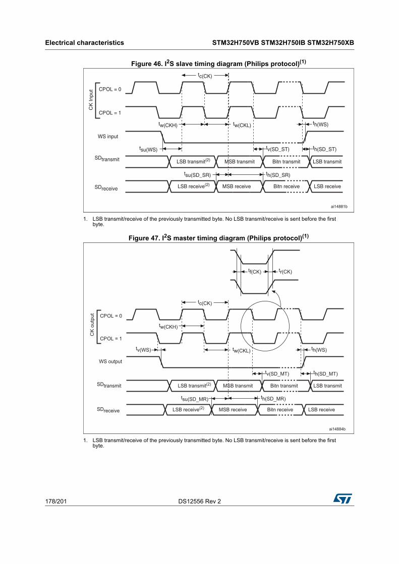
Electrical characteristics STM32H750VB STM32H750IB STM32H750XB
178/201 DS12556 Rev 2
Figure 46. I2S slave timing diagram (Philips protocol)(1)
1. LSB transmit/receive of the previously transmitted byte. No LSB transmit/receive is sent before the first byte.
Figure 47. I2S master timing diagram (Philips protocol)(1)
1. LSB transmit/receive of the previously transmitted byte. No LSB transmit/receive is sent before the first byte.

DS12556 Rev 2 179/201
STM32H750VB STM32H750IB STM32H750XB Electrical characteristics
189
SAI characteristics
Unless otherwise specified, the parameters given in Table 104 for SAI are derived from tests performed under the ambient temperature, fPCLKx frequency and VDD supply voltage conditions summarized in Table 22: General operating conditions, with the following configuration:
• Output speed is set to OSPEEDRy[1:0] = 10
• Capacitive load C=30 pF
• Measurement points are performed at CMOS levels: 0.5VDD
Refer to Section 6.3.15: I/O port characteristics for more details on the input/output alternate function characteristics (SCK,SD,WS).
Table 104. SAI characteristics(1)
Symbol Parameter Conditions Min Max Unit
fMCK SAI Main clock output - 256 x 8K 256xFs MHz
FCK SAI clock frequency(2) Master data: 32 bits - 128xFs(3)
MHzSlave data: 32 bits - 128xFs
tv(FS) FS valid time
Master mode
2.7≤VDD≤3.6V- 15
ns
Master mode
1.71≤VDD≤3.6V- 20
tsu(FS) FS setup time Slave mode 7 -
th(FS) FS hold time Master mode 1 -
Slave mode 1 -
tsu(SD_A_MR)Data input setup time
Master receiver 0.5 -
tsu(SD_B_SR) Slave receiver 1 -
th(SD_A_MR)Data input hold time
Master receiver 3.5 -
th(SD_B_SR) Slave receiver 2 -
tv(SD_B_ST) Data output valid time
Slave transmitter (after enable edge)
2.7≤VDD≤3.6V- 17
ns
Slave transmitter (after enable edge)
1.62≤VDD≤3.6V- 20
th(SD_B_ST) Data output hold time Slave transmitter (after enable edge) 7 -
tv(SD_A_MT) Data output valid time
Master transmitter (after enable edge)
2.7≤VDD≤3.6V- 17
Master transmitter (after enable edge)
1.62≤VDD≤3.6V- 20
th(SD_A_MT) Data output hold time Master transmitter (after enable edge) 7.55 -
1. Guaranteed by characterization results.
2. APB clock frequency must be at least twice SAI clock frequency.
3. With FS=192 kHz.

Electrical characteristics STM32H750VB STM32H750IB STM32H750XB
180/201 DS12556 Rev 2
Figure 48. SAI master timing waveforms
Figure 49. SAI slave timing waveforms
MDIO characteristics
The MDIO controller is mapped on APB2 domain. The frequency of the APB bus should at least 1.5 times the MDC frequency: FPCLK2 ≥ 1.5 * FMDC.
Table 105. MDIO Slave timing parameters
Symbol Parameter Min Typ Max Unit
FsDC Management data clock - - 40 MHz
td(MDIO) Management data input/output output valid time 7 8 20
nstsu(MDIO) Management data input/output setup time 4 - -
th(MDIO) Management data input/output hold time 1 - -
MS32771V1
SAI_SCK_X
SAI_FS_X(output)
1/fSCK
SAI_SD_X(transmit)
tv(FS)
Slot n
SAI_SD_X(receive)
th(FS)
Slot n+2
tv(SD_MT) th(SD_MT)
Slot n
tsu(SD_MR) th(SD_MR)
MS32772V1
SAI_SCK_X
SAI_FS_X(input)
SAI_SD_X(transmit)
tsu(FS)
Slot n
SAI_SD_X(receive)
tw(CKH_X) th(FS)
Slot n+2
tv(SD_ST) th(SD_ST)
Slot n
tsu(SD_SR)
tw(CKL_X)
th(SD_SR)
1/fSCK

DS12556 Rev 2 181/201
STM32H750VB STM32H750IB STM32H750XB Electrical characteristics
189
Figure 50. MDIO Slave timing diagram
SD/SDIO MMC card host interface (SDMMC) characteristics
Unless otherwise specified, the parameters given in Table 106 for the SDIO/MMC interface are derived from tests performed under the ambient temperature, fPCLK2 frequency and VDD supply voltage conditions summarized in Table 22: General operating conditions, with the following configuration:
• Output speed is set to OSPEEDRy[1:0] = 11
• Capacitive load C = 30 pF
• Measurement points are done at CMOS levels: 0.5VDD
• I/O compensation cell enabled
• HSLV activated when VDD ≤ 2.7 V
Refer to Section 6.3.15: I/O port characteristics for more details on the input/output characteristics.
MSv40460V1
tsu(MDIO)
tMDC)
th(MDIO)
td(MDIO)
Table 106. Dynamic characteristics: SD / MMC characteristics, VDD=2.7V to 3.6V(1)(2)
Symbol Parameter Conditions Min Typ Max Unit
fPP Clock frequency in data transfer mode - 0 - 125 MHz
tW(CKL) Clock low timefPP =50 MHz
9.5 10.5 -ns
tW(CKH) Clock high time 8.5 9.5 -
CMD, D inputs (referenced to CK) in MMC and SD HS/SDR/DDR mode
tISU Input setup time HS
fPP ≥ 50 MHz
2 - -
nstIH Input hold time HS 1.5 - -
tIDW(3) Input valid window (variable window) 3 - -
CMD, D outputs (referenced to CK) in MMC and SD HS/SDR/DDR mode
tOV Output valid time HSfPP ≥ 50 MHz
- 3.5 5ns
tOH Output hold time HS 2 - -
Electrical characteristics STM32H750VB STM32H750IB STM32H750XB
182/201 DS12556 Rev 2
CMD, D inputs (referenced to CK) in SD default mode
tISUD Input setup time SDfPP =25 MHz
2 - -ns
tIHD Input hold time SD 1.5 - -
CMD, D outputs (referenced to CK) in SD default mode
tOVD Output valid default time SDfPP =25 MHz
- 1 2ns
tOHD Output hold default time SD 0 - -
1. Guaranteed by characterization results.
2. Above 100 MHz, CL = 20 pF.
3. The minimum window of time where the data needs to be stable for proper sampling in tuning mode.
Table 106. Dynamic characteristics: SD / MMC characteristics, VDD=2.7V to 3.6V(1)(2)
Symbol Parameter Conditions Min Typ Max Unit
Table 107. Dynamic characteristics: eMMC characteristics, VDD=1.71V to 1.9V(1)(2)
Symbol Parameter Conditions Min Typ Max Unit
fPP Clock frequency in data transfer mode - 0 - 120 MHz
tW(CKL) Clock low timefPP =50 MHz
9.5 10.5 -ns
tW(CKH) Clock high time 8.5 9.5 -
CMD, D inputs (referenced to CK) in eMMC mode
tISU Input setup time HS
fPP ≥ 50 MHz
1.5 - -
nstIH Input hold time HS 2 - -
tIDW(3) Input valid window (variable window) 3.5 - -
CMD, D outputs (referenced to CK) in eMMC mode
tOV Output valid time HSfPP ≥ 50 MHz
- 5 7ns
tOH Output hold time HS 3 - -
1. Guaranteed by characterization results.
2. CL = 20 pF.
3. The minimum window of time where the data needs to be stable for proper sampling in tuning mode.

DS12556 Rev 2 183/201
STM32H750VB STM32H750IB STM32H750XB Electrical characteristics
189
Figure 51. SDIO high-speed mode
Figure 52. SD default mode
Figure 53. DDR mode
CAN (controller area network) interface
Refer to Section 6.3.15: I/O port characteristics for more details on the input/output alternate function characteristics (FDCANx_TX and FDCANx_RX).
ai14888
CK
D, CMD(output)
tOVD tOHD
MSv36879V1
Data output D0 D2 D4
Clock
Data input D0 D2 D4
t(CK) tw(CKH) tw(CKL)tr(CK) tf(CK)
tsf(IN) thf(IN)
tvf(OUT) thr(OUT)
D1 D3 D5
D1 D3 D5
tvr(OUT) thf(OUT)
tsr(IN) thr(IN)
Electrical characteristics STM32H750VB STM32H750IB STM32H750XB
184/201 DS12556 Rev 2
USB OTG_FS characteristics
The USB interface is fully compliant with the USB specification version 2.0 and is USB-IF certified (for Full-speed device operation).
USB OTG_HS characteristics
Unless otherwise specified, the parameters given in Table 109 for ULPI are derived from tests performed under the ambient temperature, frcc_c_ck frequency and VDD supply voltage conditions summarized in Table 22: General operating conditions, with the following configuration:
• Output speed is set to OSPEEDRy[1:0] = 11
• Capacitive load C = 20 pF
• Measurement points are done at CMOS levels: 0.5VDD.
Refer to Section 6.3.15: I/O port characteristics for more details on the input/output characteristics.
Table 108. USB OTG_FS electrical characteristics
Symbol Parameter Condition Min Typ Max Unit
VDD33USBUSB transceiver operating voltage
- 3.0(1)
1. The USB functionality is ensured down to 2.7 V but not the full USB electrical characteristics which are degraded in the 2.7 to 3.0 V voltage range.
- 3.6 V
RPUI Embedded USB_DP pull-up value during idle
- 900 1250 1600
ΩRPUREmbedded USB_DP pull-up value during reception
- 1400 2300 3200
ZDRV Output driver impedance(2)
2. No external termination series resistors are required on USB_DP (D+) and USB_DM (D-); the matching impedance is already included in the embedded driver.
Driver high and low
28 36 44
Table 109. Dynamic characteristics: USB ULPI(1)
Symbol Parameter Conditions Min Typ Max Unit
tSC Control in (ULPI_DIR, ULPI_NXT) setup time - 0.5 - -
ns
tHC Control in (ULPI_DIR, ULPI_NXT) hold time - 6.5 - -
tSD Data in setup time - 2.5 - -
tHD Data in hold time - 0 - -
tDC/tDD Data/control output delay
2.7 V < VDD < 3.6 V, CL = 20 pF
- 6.5 8.5
- -
6.5 131.7 V < VDD < 3.6 V,
CL = 15 pF-
1. Guaranteed by characterization results.

DS12556 Rev 2 185/201
STM32H750VB STM32H750IB STM32H750XB Electrical characteristics
189
Figure 54. ULPI timing diagram
Ethernet characteristics
Unless otherwise specified, the parameters given in Table 110, Table 111 and Table 112 for SMI, RMII and MII are derived from tests performed under the ambient temperature, frcc_c_ck frequency summarized in Table 22: General operating conditions, with the following configuration:
• Output speed is set to OSPEEDRy[1:0] = 10
• Capacitive load C = 20 pF
• Measurement points are done at CMOS levels: 0.5VDD.
Refer to Section 6.3.15: I/O port characteristics for more details on the input/output characteristics.
Table 110 gives the list of Ethernet MAC signals for the SMI and Figure 55 shows the corresponding timing diagram.
Table 110. Dynamics characteristics: Ethernet MAC signals for SMI(1)
1. Guaranteed by characterization results.
Symbol Parameter Min Typ Max Unit
tMDC MDC cycle time(2.5 MHz) 400 400 403
nsTd(MDIO) Write data valid time 1 1.5 3
tsu(MDIO) Read data setup time 8 - -
th(MDIO) Read data hold time 0 - -
Clock
Control In(ULPI_DIR,ULPI_NXT)
data In(8-bit)
Control out(ULPI_STP)
data out(8-bit)
tDD
tDC
tHDtSD
tHCtSC
ai17361c
tDC

Electrical characteristics STM32H750VB STM32H750IB STM32H750XB
186/201 DS12556 Rev 2
Figure 55. Ethernet SMI timing diagram
Table 111 gives the list of Ethernet MAC signals for the RMII and Figure 56 shows the corresponding timing diagram.
Figure 56. Ethernet RMII timing diagram
Table 112 gives the list of Ethernet MAC signals for MII and Figure 57 shows the corresponding timing diagram.
Table 111. Dynamics characteristics: Ethernet MAC signals for RMII(1)
1. Guaranteed by characterization results.
Symbol Parameter Min Typ Max Unit
tsu(RXD) Receive data setup time 2 - -
ns
tih(RXD) Receive data hold time 3 - -
tsu(CRS) Carrier sense setup time 2.5 - -
tih(CRS) Carrier sense hold time 2 - -
td(TXEN) Transmit enable valid delay time 4 4.5 7
td(TXD) Transmit data valid delay time 7 7.5 11.5
MS31384V1
ETH_MDC
ETH_MDIO(O)
ETH_MDIO(I)
tMDC
td(MDIO)
tsu(MDIO) th(MDIO)
ai15667b
RMII_REF_CLK
RMII_TX_ENRMII_TXD[1:0]
RMII_RXD[1:0]RMII_CRS_DV
td(TXEN)td(TXD)
tsu(RXD)tsu(CRS)
tih(RXD)tih(CRS)
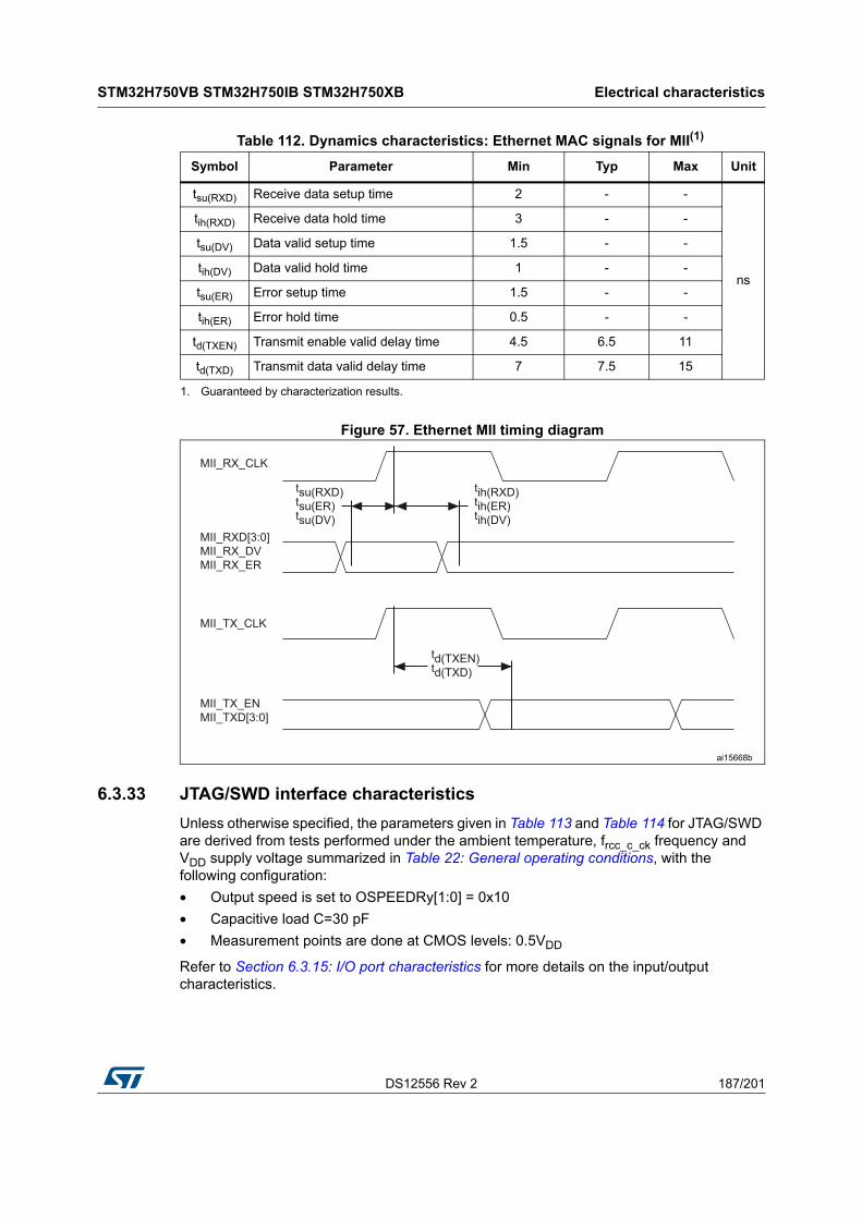
DS12556 Rev 2 187/201
STM32H750VB STM32H750IB STM32H750XB Electrical characteristics
189
Figure 57. Ethernet MII timing diagram
6.3.33 JTAG/SWD interface characteristics
Unless otherwise specified, the parameters given in Table 113 and Table 114 for JTAG/SWD are derived from tests performed under the ambient temperature, frcc_c_ck frequency and VDD supply voltage summarized in Table 22: General operating conditions, with the following configuration:
• Output speed is set to OSPEEDRy[1:0] = 0x10
• Capacitive load C=30 pF
• Measurement points are done at CMOS levels: 0.5VDD
Refer to Section 6.3.15: I/O port characteristics for more details on the input/output characteristics.
Table 112. Dynamics characteristics: Ethernet MAC signals for MII(1)
1. Guaranteed by characterization results.
Symbol Parameter Min Typ Max Unit
tsu(RXD) Receive data setup time 2 - -
ns
tih(RXD) Receive data hold time 3 - -
tsu(DV) Data valid setup time 1.5 - -
tih(DV) Data valid hold time 1 - -
tsu(ER) Error setup time 1.5 - -
tih(ER) Error hold time 0.5 - -
td(TXEN) Transmit enable valid delay time 4.5 6.5 11
td(TXD) Transmit data valid delay time 7 7.5 15
ai15668b
MII_RX_CLK
MII_RXD[3:0]MII_RX_DVMII_RX_ER
td(TXEN)td(TXD)
tsu(RXD)tsu(ER)tsu(DV)
tih(RXD)tih(ER)tih(DV)
MII_TX_CLK
MII_TX_ENMII_TXD[3:0]
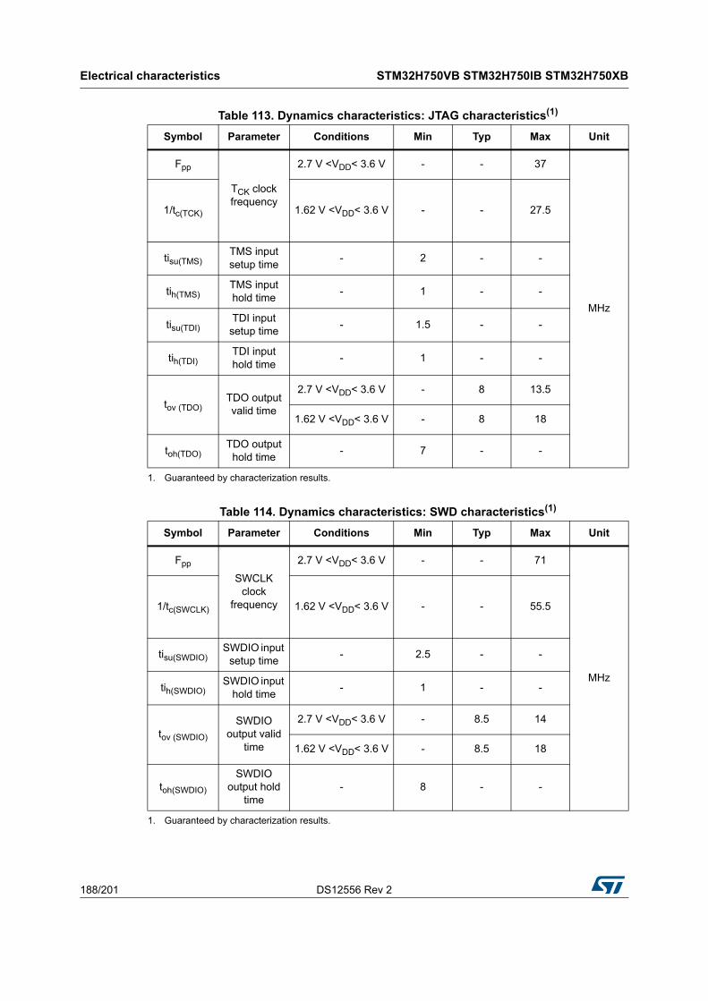
Electrical characteristics STM32H750VB STM32H750IB STM32H750XB
188/201 DS12556 Rev 2
Table 113. Dynamics characteristics: JTAG characteristics(1)
1. Guaranteed by characterization results.
Symbol Parameter Conditions Min Typ Max Unit
Fpp
TCK clock frequency
2.7 V <VDD< 3.6 V - - 37
MHz
1/tc(TCK) 1.62 V <VDD< 3.6 V - - 27.5
tisu(TMS)TMS input setup time
- 2 - -
tih(TMS)TMS input hold time
- 1 - -
tisu(TDI)TDI input
setup time- 1.5 - -
tih(TDI)TDI input hold time
- 1 - -
tov (TDO)TDO output valid time
2.7 V <VDD< 3.6 V - 8 13.5
1.62 V <VDD< 3.6 V - 8 18
toh(TDO)TDO output
hold time - 7 - -
Table 114. Dynamics characteristics: SWD characteristics(1)
1. Guaranteed by characterization results.
Symbol Parameter Conditions Min Typ Max Unit
Fpp
SWCLK clock
frequency
2.7 V <VDD< 3.6 V - - 71
MHz
1/tc(SWCLK) 1.62 V <VDD< 3.6 V - - 55.5
tisu(SWDIO)SWDIO input
setup time- 2.5 - -
tih(SWDIO)SWDIO input
hold time- 1 - -
tov (SWDIO)
SWDIO output valid
time
2.7 V <VDD< 3.6 V - 8.5 14
1.62 V <VDD< 3.6 V - 8.5 18
toh(SWDIO)
SWDIO output hold
time - 8 - -
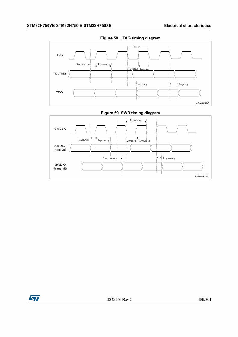
DS12556 Rev 2 189/201
STM32H750VB STM32H750IB STM32H750XB Electrical characteristics
189
Figure 58. JTAG timing diagram
Figure 59. SWD timing diagram
MSv40458V1
TDI/TMS
TCK
TDO
tc(TCK)
tw(TCKL) tw(TCKH)
th(TMS/TDI)tsu(TMS/TDI)
tov(TDO) toh(TDO)
MSv40459V1
SWDIO
SWCLK
SWDIO
tc(SWCLK)
twSWCLKL) tw(SWCLKH)th(SWDIO)tsu(SWDIO)
tov(SWDIO) toh(SWDIO)
(receive)
(transmit)
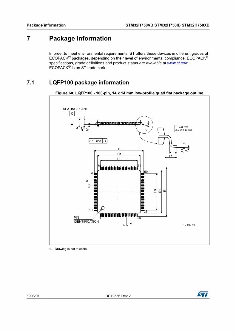
Package information STM32H750VB STM32H750IB STM32H750XB
190/201 DS12556 Rev 2
7 Package information
In order to meet environmental requirements, ST offers these devices in different grades of ECOPACK® packages, depending on their level of environmental compliance. ECOPACK® specifications, grade definitions and product status are available at www.st.com. ECOPACK® is an ST trademark.
7.1 LQFP100 package information
Figure 60. LQFP100 - 100-pin, 14 x 14 mm low-profile quad flat package outline
1. Drawing is not to scale.
eIDENTIFICATIONPIN 1
GAUGE PLANE0.25 mm
SEATING PLANE
DD1D3
E3 E1 E
K
ccc C
C
1 25
26100
76
75 51
50
1L_ME_V5
A2A A1
L1L
c
b
A1

DS12556 Rev 2 191/201
STM32H750VB STM32H750IB STM32H750XB Package information
199
Table 115. LQPF100 - 100-pin, 14 x 14 mm low-profile quad flat package mechanical data
Symbolmillimeters inches(1)
1. Values in inches are converted from mm and rounded to 4 decimal digits.
Min Typ Max Min Typ Max
A - - 1.600 - - 0.0630
A1 0.050 - 0.150 0.0020 - 0.0059
A2 1.350 1.400 1.450 0.0531 0.0551 0.0571
b 0.170 0.220 0.270 0.0067 0.0087 0.0106
c 0.090 - 0.200 0.0035 - 0.0079
D 15.800 16.000 16.200 0.6220 0.6299 0.6378
D1 13.800 14.000 14.200 0.5433 0.5512 0.5591
D3 - 12.000 - - 0.4724 -
E 15.800 16.000 16.200 0.6220 0.6299 0.6378
E1 13.800 14.000 14.200 0.5433 0.5512 0.5591
E3 - 12.000 - - 0.4724 -
e - 0.500 - - 0.0197 -
L 0.450 0.600 0.750 0.0177 0.0236 0.0295
L1 - 1.000 - - 0.0394 -
k 0.0° 3.5° 7.0° 0.0° 3.5° 7.0°
ccc - - 0.080 - - 0.0031
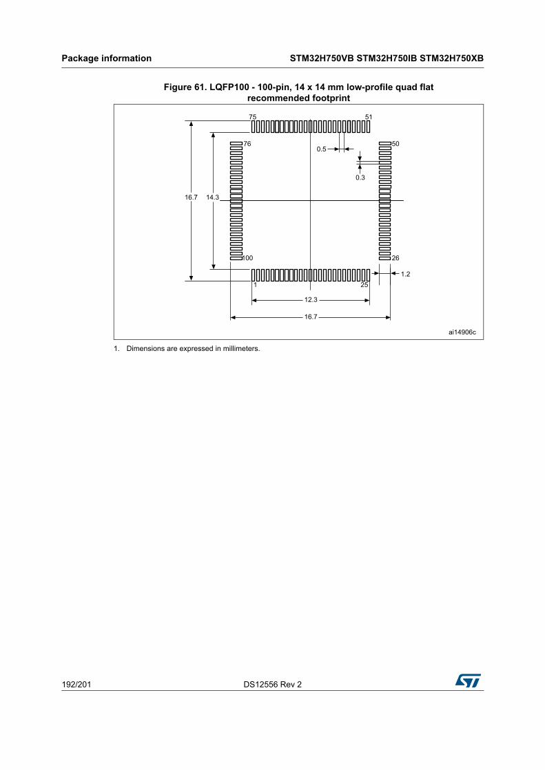
Package information STM32H750VB STM32H750IB STM32H750XB
192/201 DS12556 Rev 2
Figure 61. LQFP100 - 100-pin, 14 x 14 mm low-profile quad flat recommended footprint
1. Dimensions are expressed in millimeters.
75 51
50760.5
0.3
16.7 14.3
100 26
12.3
251.2
16.7
1
ai14906c
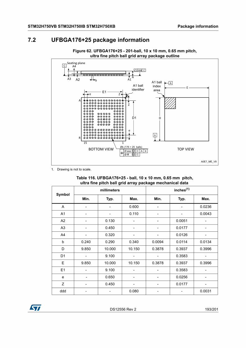
DS12556 Rev 2 193/201
STM32H750VB STM32H750IB STM32H750XB Package information
199
7.2 UFBGA176+25 package information
Figure 62. UFBGA176+25 - 201-ball, 10 x 10 mm, 0.65 mm pitch, ultra fine pitch ball grid array package outline
1. Drawing is not to scale.
Table 116. UFBGA176+25 - ball, 10 x 10 mm, 0.65 mm pitch, ultra fine pitch ball grid array package mechanical data
Symbolmillimeters inches(1)
Min. Typ. Max. Min. Typ. Max.
A - - 0.600 - - 0.0236
A1 - - 0.110 - - 0.0043
A2 - 0.130 - - 0.0051 -
A3 - 0.450 - - 0.0177 -
A4 - 0.320 - - 0.0126 -
b 0.240 0.290 0.340 0.0094 0.0114 0.0134
D 9.850 10.000 10.150 0.3878 0.3937 0.3996
D1 - 9.100 - - 0.3583 -
E 9.850 10.000 10.150 0.3878 0.3937 0.3996
E1 - 9.100 - - 0.3583 -
e - 0.650 - - 0.0256 -
Z - 0.450 - - 0.0177 -
ddd - - 0.080 - - 0.0031
A0E7_ME_V8
D1
Seating plane
A3
Cddd
A1A
e Z
Z
e
R
A
15 1
BOTTOM VIEW
E
D
TOP VIEWØb (176 + 25 balls)
B
A
BeeeØ MfffØ M
CC
A
C
A1 ball identifier
A1 ball index area
b
A4
E1
A2

Package information STM32H750VB STM32H750IB STM32H750XB
194/201 DS12556 Rev 2
Figure 63. UFBGA176+25 - 201-ball, 10 x 10 mm, 0.65 mm pitch, ultra fine pitch ballgrid array package recommended footprint
eee - - 0.150 - - 0.0059
fff - - 0.050 - - 0.0020
1. Values in inches are converted from mm and rounded to 4 decimal digits.
Table 117. UFBGA 176+25 recommended PCB design rules (0.65 mm pitch BGA)
Dimension Recommended values
Pitch 0.65 mm
Dpad 0.300 mm
Dsm0.400 mm typ. (depends on the soldermask registration tolerance)
Stencil opening 0.300 mm
Stencil thickness Between 0.100 mm and 0.125 mm
Pad trace width 0.100 mm
Table 116. UFBGA176+25 - ball, 10 x 10 mm, 0.65 mm pitch, ultra fine pitch ball grid array package mechanical data (continued)
Symbolmillimeters inches(1)
Min. Typ. Max. Min. Typ. Max.
A0E7_FP_V1
DpadDsm
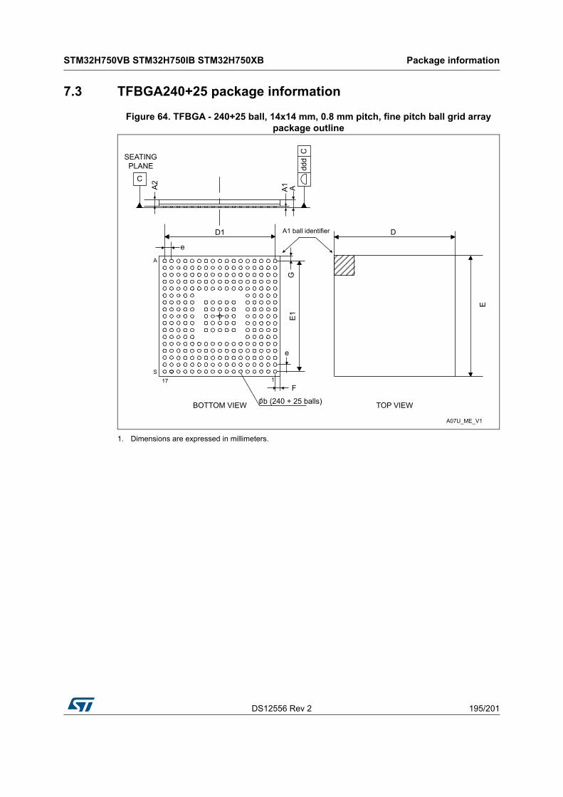
DS12556 Rev 2 195/201
STM32H750VB STM32H750IB STM32H750XB Package information
199
7.3 TFBGA240+25 package information
Figure 64. TFBGA - 240+25 ball, 14x14 mm, 0.8 mm pitch, fine pitch ball grid arraypackage outline
1. Dimensions are expressed in millimeters.
C
SEATING PLANE dd
d C
AA1A2
D1
F
E1
E
D
G
e
A
S17 1
b (240 + 25 balls)BOTTOM VIEW
e
A1 ball identifier
TOP VIEW
A07U_ME_V1
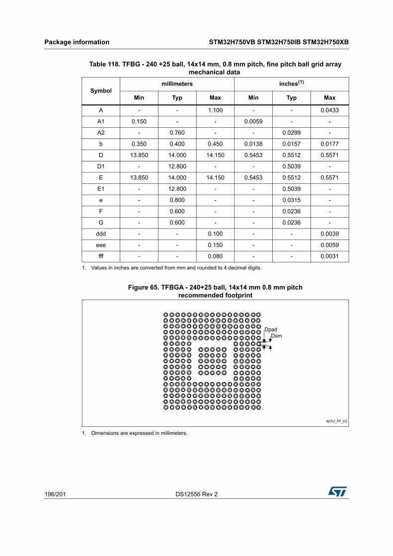
Package information STM32H750VB STM32H750IB STM32H750XB
196/201 DS12556 Rev 2
Figure 65. TFBGA - 240+25 ball, 14x14 mm 0.8 mm pitchrecommended footprint
1. Dimensions are expressed in millimeters.
Table 118. TFBG - 240 +25 ball, 14x14 mm, 0.8 mm pitch, fine pitch ball grid arraymechanical data
Symbolmillimeters inches(1)
1. Values in inches are converted from mm and rounded to 4 decimal digits.
Min Typ Max Min Typ Max
A - - 1.100 - - 0.0433
A1 0.150 - - 0.0059 - -
A2 - 0.760 - - 0.0299 -
b 0.350 0.400 0.450 0.0138 0.0157 0.0177
D 13.850 14.000 14.150 0.5453 0.5512 0.5571
D1 - 12.800 - - 0.5039 -
E 13.850 14.000 14.150 0.5453 0.5512 0.5571
E1 - 12.800 - - 0.5039 -
e - 0.800 - - 0.0315 -
F - 0.600 - - 0.0236 -
G - 0.600 - - 0.0236 -
ddd - - 0.100 - - 0.0039
eee - - 0.150 - - 0.0059
fff - - 0.080 - - 0.0031
A07U_FP_V2
DpadDsm
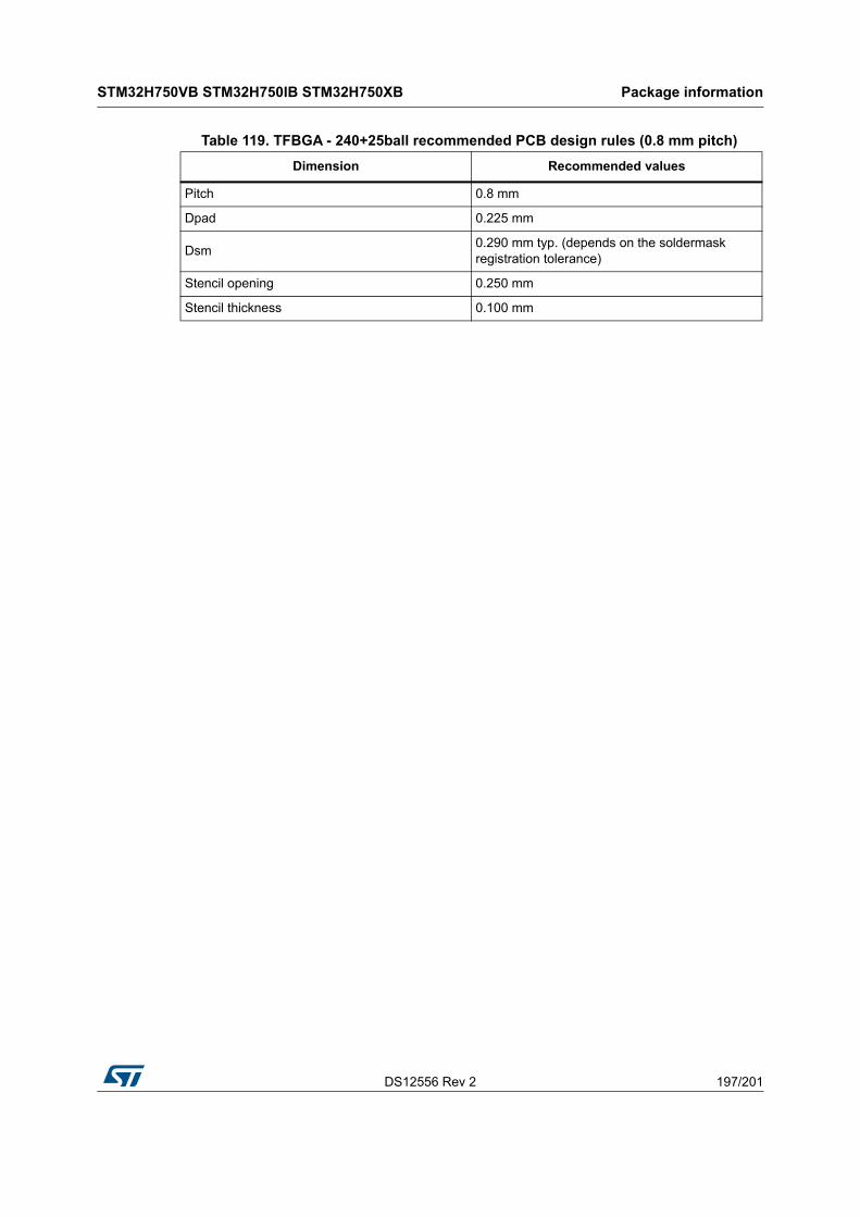
DS12556 Rev 2 197/201
STM32H750VB STM32H750IB STM32H750XB Package information
199
Table 119. TFBGA - 240+25ball recommended PCB design rules (0.8 mm pitch)
Dimension Recommended values
Pitch 0.8 mm
Dpad 0.225 mm
Dsm0.290 mm typ. (depends on the soldermask registration tolerance)
Stencil opening 0.250 mm
Stencil thickness 0.100 mm
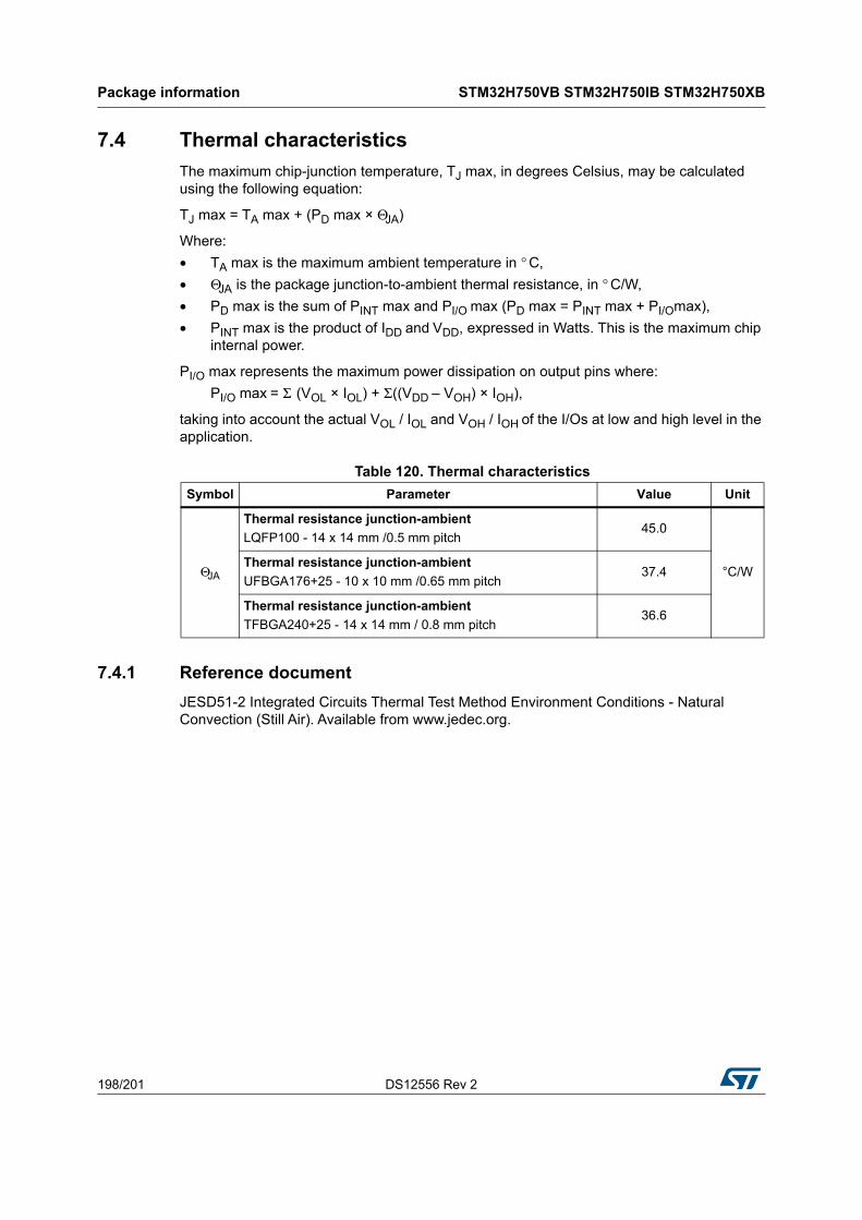
Package information STM32H750VB STM32H750IB STM32H750XB
198/201 DS12556 Rev 2
7.4 Thermal characteristics
The maximum chip-junction temperature, TJ max, in degrees Celsius, may be calculated using the following equation:
TJ max = TA max + (PD max × ΘJA)
Where:
• TA max is the maximum ambient temperature in ° C,
• ΘJA is the package junction-to-ambient thermal resistance, in ° C/W,
• PD max is the sum of PINT max and PI/O max (PD max = PINT max + PI/Omax),
• PINT max is the product of IDD and VDD, expressed in Watts. This is the maximum chip internal power.
PI/O max represents the maximum power dissipation on output pins where:
PI/O max = Σ (VOL × IOL) + Σ((VDD – VOH) × IOH),
taking into account the actual VOL / IOL and VOH / IOH of the I/Os at low and high level in the application.
7.4.1 Reference document
JESD51-2 Integrated Circuits Thermal Test Method Environment Conditions - Natural Convection (Still Air). Available from www.jedec.org.
Table 120. Thermal characteristics
Symbol Parameter Value Unit
ΘJA
Thermal resistance junction-ambient
LQFP100 - 14 x 14 mm /0.5 mm pitch45.0
°C/WThermal resistance junction-ambient
UFBGA176+25 - 10 x 10 mm /0.65 mm pitch37.4
Thermal resistance junction-ambient
TFBGA240+25 - 14 x 14 mm / 0.8 mm pitch36.6
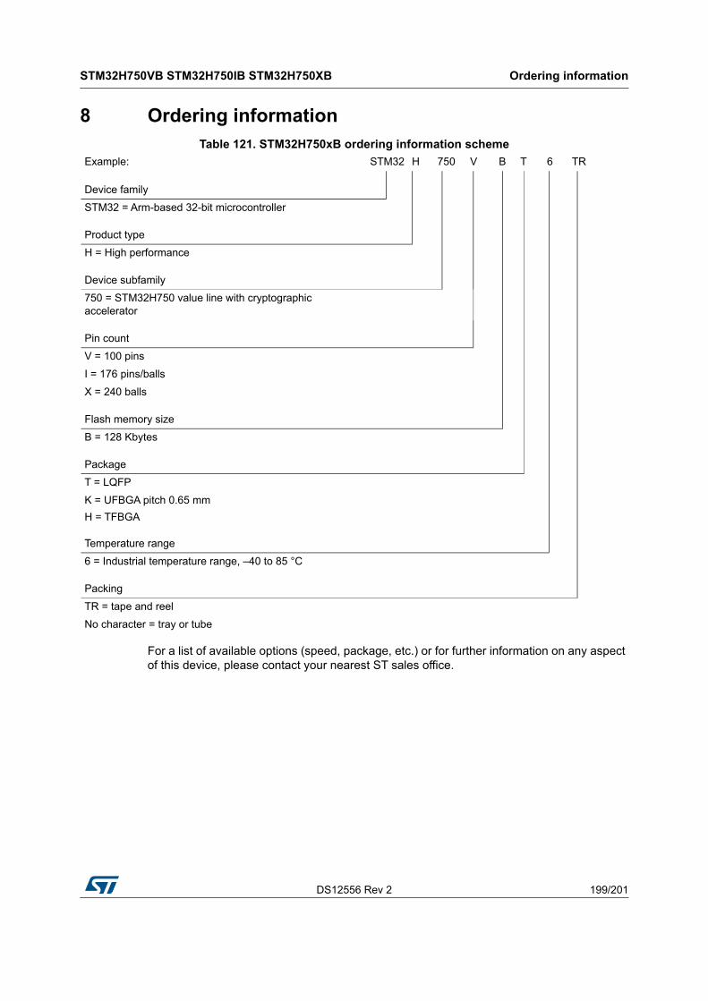
DS12556 Rev 2 199/201
STM32H750VB STM32H750IB STM32H750XB Ordering information
199
8 Ordering information
For a list of available options (speed, package, etc.) or for further information on any aspect of this device, please contact your nearest ST sales office.
Table 121. STM32H750xB ordering information scheme
Example: STM32 H 750 V B T 6 TR
Device family
STM32 = Arm-based 32-bit microcontroller
Product type
H = High performance
Device subfamily
750 = STM32H750 value line with cryptographic accelerator
Pin count
V = 100 pins
I = 176 pins/balls
X = 240 balls
Flash memory size
B = 128 Kbytes
Package
T = LQFP
K = UFBGA pitch 0.65 mm
H = TFBGA
Temperature range
6 = Industrial temperature range, –40 to 85 °C
Packing
TR = tape and reel
No character = tray or tube
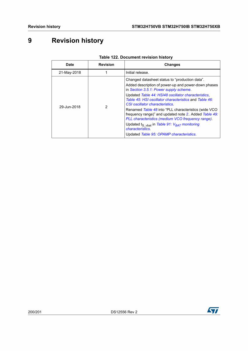
Revision history STM32H750VB STM32H750IB STM32H750XB
200/201 DS12556 Rev 2
9 Revision history
Table 122. Document revision history
Date Revision Changes
21-May-2018 1 Initial release.
29-Jun-2018 2
Changed datasheet status to “production data”.
Added description of power-up and power-down phases in Section 3.5.1: Power supply scheme.
Updated Table 44: HSI48 oscillator characteristics, Table 45: HSI oscillator characteristics and Table 46: CSI oscillator characteristics.
Renamed Table 48 into “PLL characteristics (wide VCO frequency range)” and updated note 2.. Added Table 49: PLL characteristics (medium VCO frequency range).
Updated tS_vbat in Table 91: VBAT monitoring characteristics.
Updated Table 95: OPAMP characteristics.
DS12556 Rev 2 201/201
STM32H750VB STM32H750IB STM32H750XB
201
IMPORTANT NOTICE – PLEASE READ CAREFULLY
STMicroelectronics NV and its subsidiaries (“ST”) reserve the right to make changes, corrections, enhancements, modifications, and improvements to ST products and/or to this document at any time without notice. Purchasers should obtain the latest relevant information on ST products before placing orders. ST products are sold pursuant to ST’s terms and conditions of sale in place at the time of order acknowledgement.
Purchasers are solely responsible for the choice, selection, and use of ST products and ST assumes no liability for application assistance or the design of Purchasers’ products.
No license, express or implied, to any intellectual property right is granted by ST herein.
Resale of ST products with provisions different from the information set forth herein shall void any warranty granted by ST for such product.
ST and the ST logo are trademarks of ST. All other product or service names are the property of their respective owners.
Information in this document supersedes and replaces information previously supplied in any prior versions of this document.
© 2018 STMicroelectronics – All rights reserved
Related Documents