Datasheet 5A 240KHZ 36V PWM Buck DC/DC Converter TD7590 September, 2006 Techcode Semiconductor Limited 1 General Description The TD7590 is a 240 KHz fixed frequency monolithic step down switch mode regulator with a built in internal Power MOSFET. It achieves 5A continuous output current over a wide input supply range with excellent load and line regulation. The device includes a voltage reference, oscillation circuit, error amplifier, internal PMOS and etc. The PWM control circuit is able to adjust the duty ratio linearly from 0 to 100%. An enable function, an over current protection function and a short circuit protection function are built inside. An internal compensation block is built in to minimize external component count. The TD7590 serves as ideal power supply units for portable devices. Features 5A Constant Output Current 80mΩ R DSON Internal Power PMOSFET Switch Up to 95% Efficiency Fixed 240KHz Frequency Wide 3.6V to 36V Input Voltage Range Output Adjustable from 1.222V to 34V Built in Frequency Compensation Built in Thermal Shutdown Function Built in Current Limit Function TO-263 Package is Available The minimum dropout up to 0.3V Applications Portable DVD LCD Monitor / TV Battery Charger ADSL Modem Telecom / Networking Equipment Figure 1 Package Type of TD7590 TO263-5L

Welcome message from author
This document is posted to help you gain knowledge. Please leave a comment to let me know what you think about it! Share it to your friends and learn new things together.
Transcript
Datasheet
5A 240KHZ 36V PWM Buck DC/DC Converter TD7590
September, 2006 Techcode Semiconductor Limited
1
General Description The TD7590 is a 240 KHz fixed frequency monolithic step down switch mode regulator with a built in internal Power MOSFET. It achieves 5A continuous output current over a wide input supply range with excellent load and line regulation. The device includes a voltage reference, oscillation circuit, error amplifier, internal PMOS and etc. The PWM control circuit is able to adjust the duty ratio linearly from 0 to 100%. An enable function, an over current protection function and a short circuit protection function are built inside. An internal compensation block is built in to minimize external component count. The TD7590 serves as ideal power supply units for portable devices.
Features 5A Constant Output Current 80mΩ RDSON Internal Power PMOSFET
Switch Up to 95% Efficiency Fixed 240KHz Frequency Wide 3.6V to 36V Input Voltage Range Output Adjustable from 1.222V to 34V Built in Frequency Compensation Built in Thermal Shutdown Function Built in Current Limit Function TO-263 Package is Available The minimum dropout up to 0.3V
Applications Portable DVD LCD Monitor / TV Battery Charger ADSL Modem Telecom / Networking Equipment
Figure 1 Package Type of TD7590
TO263-5L
Datasheet
5A 240KHZ 36V PWM Buck DC/DC Converter TD7590
September, 2006 Techcode Semiconductor Limited
2
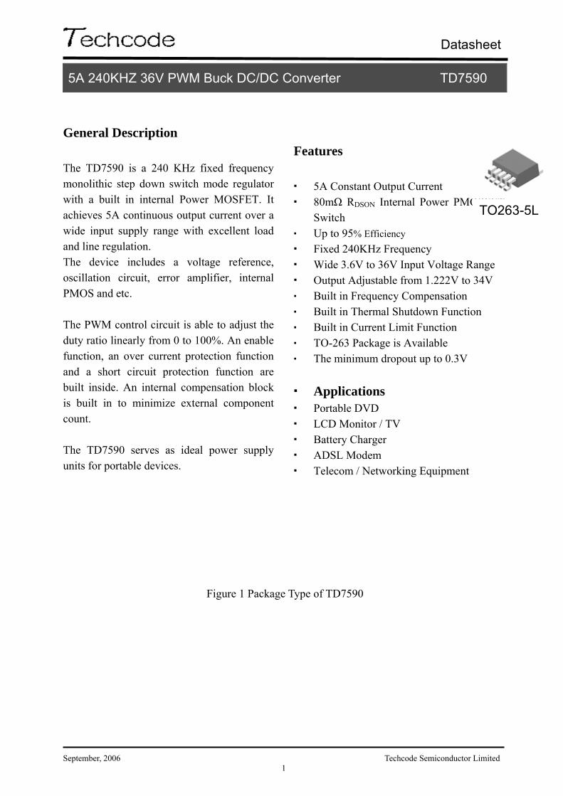
Pin Configurations
EXPOSED PAD ON BACKSIDE CONNECT TO PIN3
Figure 2 Pin Configuration of TD7590 (Top View)
Pin Description
Pin Number Pin Name Description
1 Vin Supply Voltage Input Pin. TD7590 operates from a 3.6V to 36V DC voltage. Bypass Vin to GND with a suitably large capacitor to eliminate noise on the input.
3 Output Power Switch Output Pin. SW is the switch node that supplies power to the output.
2 GND
Ground Pin. Care must be taken in layout. This pin should be placed outside of the Schottky Diode to output capacitor ground path to prevent switching current spikes from inducing voltage noise into TD7590.
4 FB Feedback Pin. Through an external resistor divider network, FB senses the output voltage and regulates it. The feedback threshold voltage is 1.222V.
5 EN Enable Pin. EN is a digital input that turns the regulator on or off .Drive EN pin high to turn on the regulator, drive it low to turn it off.
Ordering Information
X XTD7590
Circuit Type
Package
S: TO263-5L
Packing Blank: Tube R: Type and Reel
5 ON/OFF 4 Feedback 3 Output 2 Gnd 1 Vin
TO263-5L
Datasheet
5A 240KHZ 36V PWM Buck DC/DC Converter TD7590
September, 2006 Techcode Semiconductor Limited
3
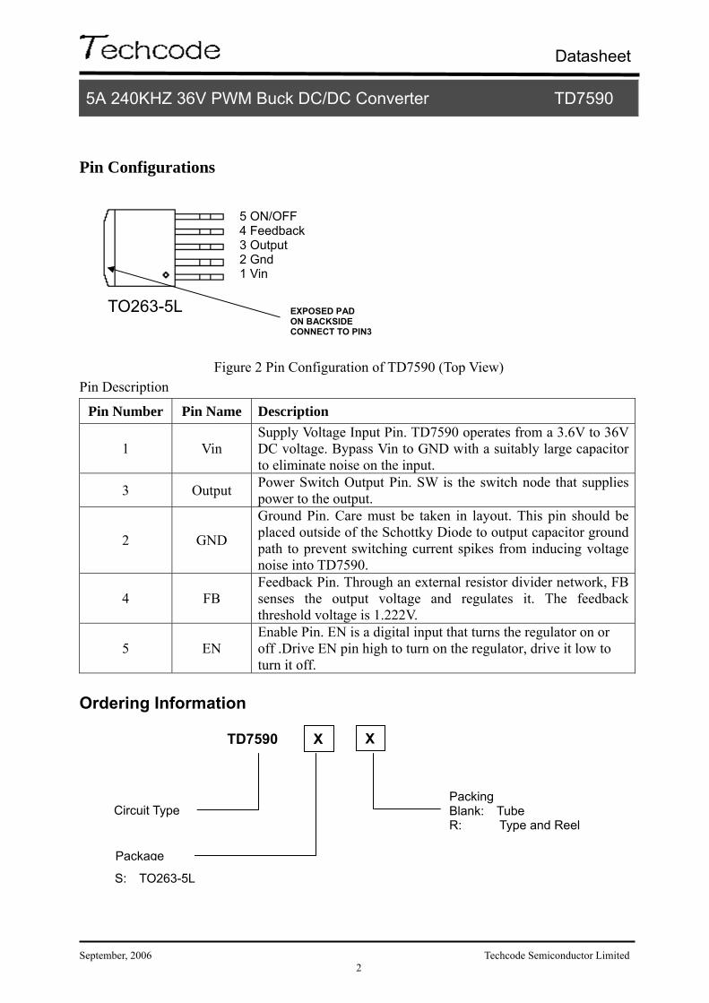
Function Block
Figure 3 Function Block Diagram of TD7590
Absolute Maximum Ratings Parameter Symbol Value Unit
Input Voltage VIN -0.3 to 36 V Feedback Pin Voltage VFB -0.3 to Vin V Enable Pin Voltage VEN -0.3 to 12 V Switch Pin Voltage VSW -0.3 to Vin V Output Power Limited Pout 36 W Operating Junction Temperature TJ 150 ºC Storage Temperature TSTG -65 to 150 ºC Lead Temperature (Soldering, 10 sec) TLEAD 260 ºC ESD (HBM) 2000 V Thermal Resistance-Junction to Ambient RθJA 23 ºC / W Thermal Resistance-Junction to Case RθJC 3.5 ºC / W
Note1: Stresses greater than those listed under Maximum Ratings may cause permanent damage to the device. This is a stress rating only and functional operation of the device at these or any other conditions above those indicated in the operation is not implied. Exposure to absolute maximum rating conditions for extended periods may affect reliability.
Datasheet
5A 240KHZ 36V PWM Buck DC/DC Converter TD7590
September, 2006 Techcode Semiconductor Limited
4
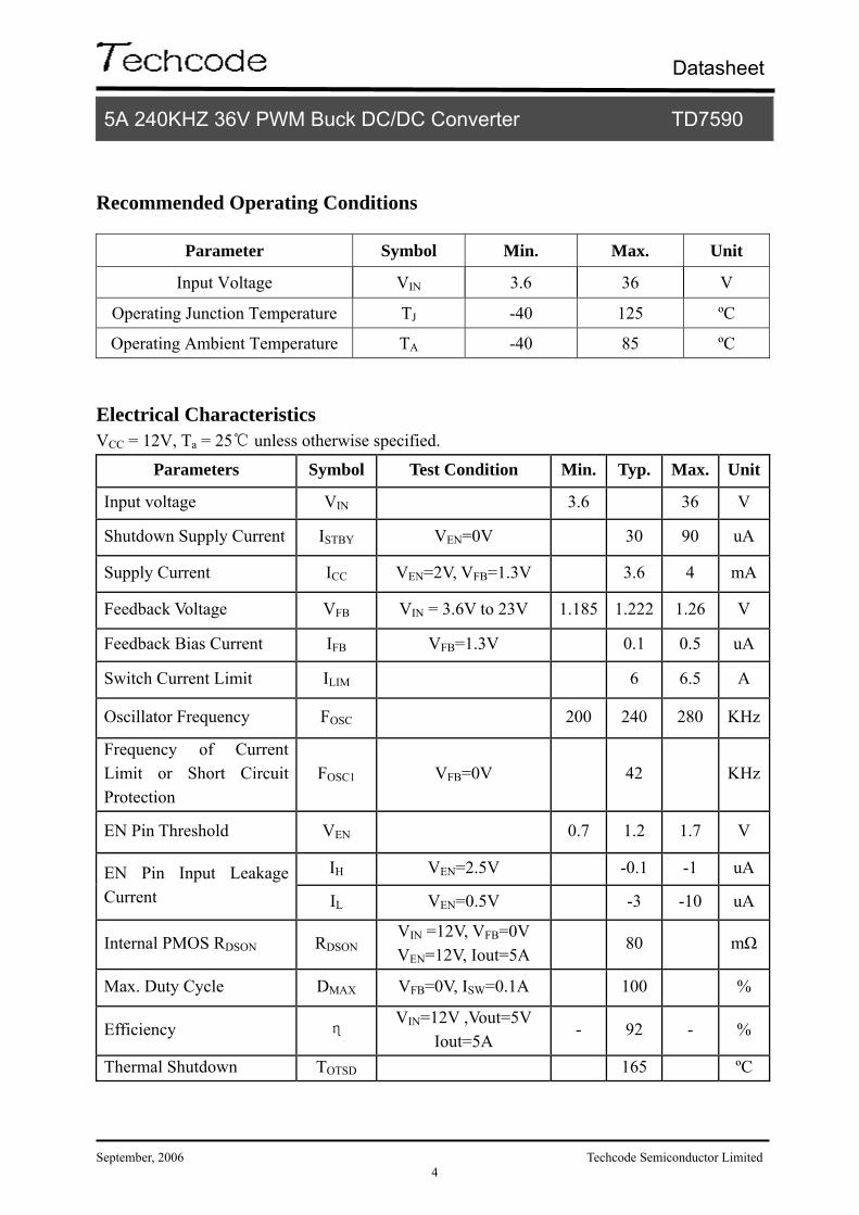
Recommended Operating Conditions
Parameter Symbol Min. Max. Unit
Input Voltage VIN 3.6 36 V
Operating Junction Temperature TJ -40 125 ºC
Operating Ambient Temperature TA -40 85 ºC Electrical Characteristics VCC = 12V, Ta = 25 unless otherwise specified.
Parameters Symbol Test Condition Min. Typ. Max. Unit
Input voltage VIN 3.6 36 V
Shutdown Supply Current ISTBY VEN=0V 30 90 uA
Supply Current ICC VEN=2V, VFB=1.3V 3.6 4 mA
Feedback Voltage VFB VIN = 3.6V to 23V 1.185 1.222 1.26 V
Feedback Bias Current IFB VFB=1.3V 0.1 0.5 uA
Switch Current Limit ILIM 6 6.5 A
Oscillator Frequency FOSC 200 240 280 KHz
Frequency of Current Limit or Short Circuit Protection
FOSC1 VFB=0V 42 KHz
EN Pin Threshold VEN 0.7 1.2 1.7 V
EN Pin Input Leakage Current
IH VEN=2.5V -0.1 -1 uA
IL VEN=0.5V -3 -10 uA
Internal PMOS RDSON RDSON VIN =12V, VFB=0V VEN=12V, Iout=5A
80 mΩ
Max. Duty Cycle DMAX VFB=0V, ISW=0.1A 100 %
Efficiency η VIN=12V ,Vout=5V
Iout=5A - 92 - %
Thermal Shutdown TOTSD 165 ºC
Datasheet
5A 240KHZ 36V PWM Buck DC/DC Converter TD7590
September, 2006 Techcode Semiconductor Limited
5
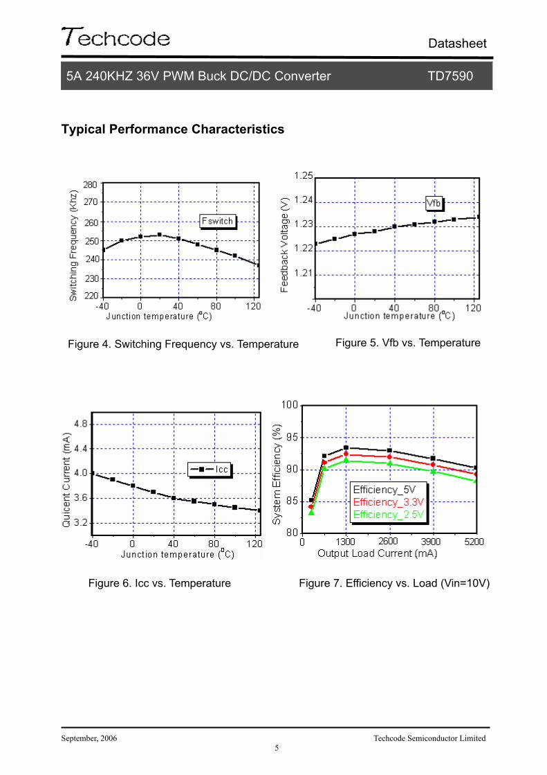
Typical Performance Characteristics
Figure 5. Vfb vs. Temperature
Figure 6. Icc vs. Temperature Figure 7. Efficiency vs. Load (Vin=10V)
Figure 4. Switching Frequency vs. Temperature
Datasheet
5A 240KHZ 36V PWM Buck DC/DC Converter TD7590
September, 2006 Techcode Semiconductor Limited
6
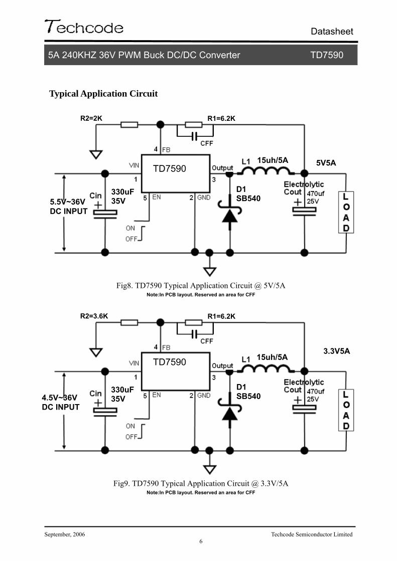
Typical Application Circuit
Fig8. TD7590 Typical Application Circuit @ 5V/5A
Note:In PCB layout. Reserved an area for CFF
Fig9. TD7590 Typical Application Circuit @ 3.3V/5A
Note:In PCB layout. Reserved an area for CFF
TD7590
TD7590
5.5V~36V DC INPUT
4.5V~36V DC INPUT
5V5A
3.3V5A
R2=2K R1=6.2K
R2=3.6K R1=6.2K
15uh/5A
15uh/5A
D1 SB540
D1 SB540
330uF 35V
330uF 35V
Datasheet
5A 240KHZ 36V PWM Buck DC/DC Converter TD7590
September, 2006 Techcode Semiconductor Limited
7
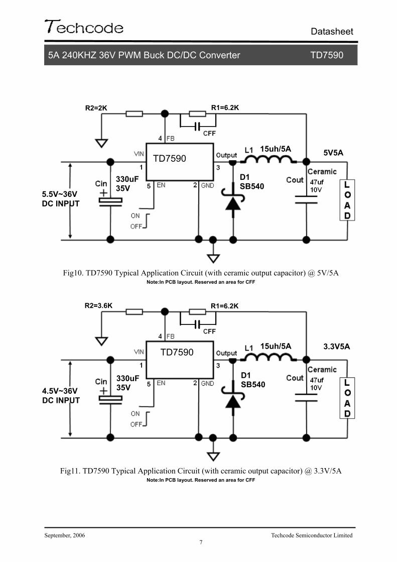
Fig10. TD7590 Typical Application Circuit (with ceramic output capacitor) @ 5V/5A
Note:In PCB layout. Reserved an area for CFF
Fig11. TD7590 Typical Application Circuit (with ceramic output capacitor) @ 3.3V/5A
Note:In PCB layout. Reserved an area for CFF
TD7590
TD7590
5.5V~36V DC INPUT
4.5V~36V DC INPUT
5V5A
3.3V5A
R2=2K R1=6.2K
R2=3.6K R1=6.2K
15uh/5A
15uh/5A
D1 SB540
D1 SB540
330uF 35V
330uF 35V
Datasheet
5A 240KHZ 36V PWM Buck DC/DC Converter TD7590
September, 2006 Techcode Semiconductor Limited
8
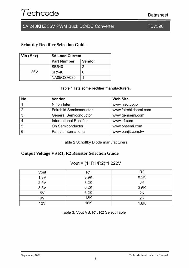
Schottky Rectifier Selection Guide Vin (Max) 5A Load Current
Part Number Vendor
36V SB540 2 SR540 6 NA05QSA035 1
Table 1 lists some rectifier manufacturers.
No. Vendor Web Site 1 Nihon Inter www.niec.co.jp 2 Fairchild Semiconductor www.fairchildsemi.com 3 General Semiconductor www.gensemi.com 4 International Rectifier www.irf.com 5 On Semiconductor www.onsemi.com 6 Pan Jit International www.panjit.com.tw
Table 2 Schottky Diode manufacturers.
Output Voltage VS R1, R2 Resistor Selection Guide
Vout = (1+R1/R2)*1.222V
Vout R1 R2 1.8V 3.9K 8.2K 2.5V 3.2K 3K 3.3V 6.2K 3.6K 5V 6.2K 2K 9V 13K 2K 12V 16K 1.8K
Table 3. Vout VS. R1, R2 Select Table
Datasheet
5A 240KHZ 36V PWM Buck DC/DC Converter TD7590
September, 2006 Techcode Semiconductor Limited
9
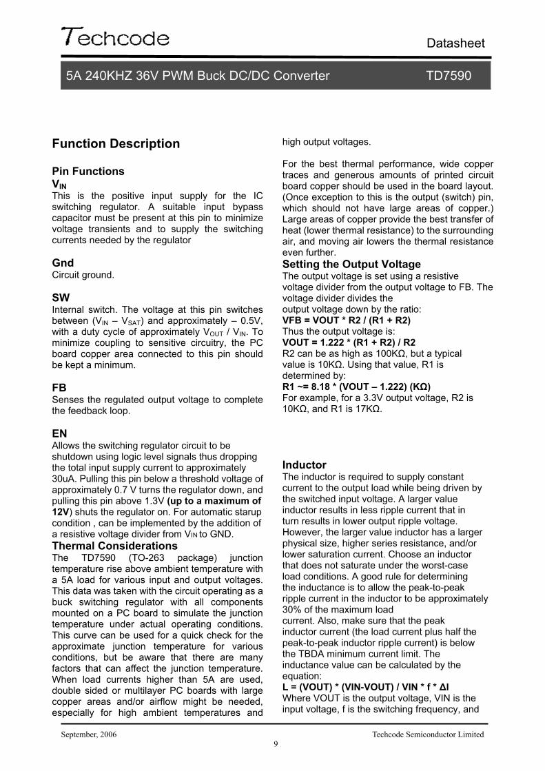
Function Description Pin Functions VIN This is the positive input supply for the IC switching regulator. A suitable input bypass capacitor must be present at this pin to minimize voltage transients and to supply the switching currents needed by the regulator Gnd Circuit ground. SW Internal switch. The voltage at this pin switches between (VIN – VSAT) and approximately – 0.5V, with a duty cycle of approximately VOUT / VIN. To minimize coupling to sensitive circuitry, the PC board copper area connected to this pin should be kept a minimum. FB Senses the regulated output voltage to complete the feedback loop. EN Allows the switching regulator circuit to be shutdown using logic level signals thus dropping the total input supply current to approximately 30uA. Pulling this pin below a threshold voltage of approximately 0.7 V turns the regulator down, and pulling this pin above 1.3V (up to a maximum of 12V) shuts the regulator on. For automatic starup condition , can be implemented by the addition of a resistive voltage divider from VIN to GND. Thermal Considerations The TD7590 (TO-263 package) junction temperature rise above ambient temperature with a 5A load for various input and output voltages. This data was taken with the circuit operating as a buck switching regulator with all components mounted on a PC board to simulate the junction temperature under actual operating conditions. This curve can be used for a quick check for the approximate junction temperature for various conditions, but be aware that there are many factors that can affect the junction temperature. When load currents higher than 5A are used, double sided or multilayer PC boards with large copper areas and/or airflow might be needed, especially for high ambient temperatures and
high output voltages. For the best thermal performance, wide copper traces and generous amounts of printed circuit board copper should be used in the board layout. (Once exception to this is the output (switch) pin, which should not have large areas of copper.) Large areas of copper provide the best transfer of heat (lower thermal resistance) to the surrounding air, and moving air lowers the thermal resistance even further. Setting the Output Voltage The output voltage is set using a resistive voltage divider from the output voltage to FB. The voltage divider divides the output voltage down by the ratio: VFB = VOUT * R2 / (R1 + R2) Thus the output voltage is: VOUT = 1.222 * (R1 + R2) / R2 R2 can be as high as 100KΩ, but a typical value is 10KΩ. Using that value, R1 is determined by: R1 ~= 8.18 * (VOUT – 1.222) (KΩ) For example, for a 3.3V output voltage, R2 is 10KΩ, and R1 is 17KΩ. Inductor The inductor is required to supply constant current to the output load while being driven by the switched input voltage. A larger value inductor results in less ripple current that in turn results in lower output ripple voltage. However, the larger value inductor has a larger physical size, higher series resistance, and/or lower saturation current. Choose an inductor that does not saturate under the worst-case load conditions. A good rule for determining the inductance is to allow the peak-to-peak ripple current in the inductor to be approximately 30% of the maximum load current. Also, make sure that the peak inductor current (the load current plus half the peak-to-peak inductor ripple current) is below the TBDA minimum current limit. The inductance value can be calculated by the equation: L = (VOUT) * (VIN-VOUT) / VIN * f * ∆I Where VOUT is the output voltage, VIN is the input voltage, f is the switching frequency, and
Datasheet
5A 240KHZ 36V PWM Buck DC/DC Converter TD7590
September, 2006 Techcode Semiconductor Limited
10
∆I is the peak-to-peak inductor ripple current. Input Capacitor The input current to the step-down converter is discontinuous, and so a capacitor is required to supply the AC current to the step-down converter while maintaining the DC input voltage. A low ESR capacitor is required to keep the noise at the IC to a minimum. Ceramic capacitors are preferred, but tantalum or low-ESR electrolytic capacitors may also suffice. The input capacitor value should be greater than 10μF. The capacitor can be electrolytic, tantalum or ceramic. However since it absorbs the input switching current it requires an adequate ripple current rating. Its RMS current rating should be greater than approximately 1/2 of the DC load current. For insuring stable operation should be placed as close to the IC as possible. Alternately a smaller high quality ceramic 0.1μF capacitor may be placed closer to the IC and a larger capacitor placed further away. If using this technique, it is recommended that the larger capacitor be a tantalum or electrolytic type. All ceramic capacitors should be places close to the TD7590. Output Capacitor The output capacitor is required to maintain the DC output voltage. Low ESR capacitors are preferred to keep the output voltage ripple low. The characteristics of the output capacitor also affect the stability of the regulation control system. Ceramic, tantalum, or low ESR electrolytic capacitors are recommended. In the case of ceramic capacitors, the impedance at the switching frequency is dominated by the capacitance, and so the output voltage ripple is mostly independent of the ESR. The output voltage ripple is estimated to be: VRIPPLE ~= 1.4 * VIN * (fLC/fSW)^2 Where VRIPPLE is the output ripple voltage, VIN is the input voltage, fLC is the resonant frequency of the LC filter, fSW is the switching frequency. In the case of tanatalum or low- ESR electrolytic capacitors, the ESR dominates the impedance at the switching frequency, and so the output ripple is calculated as: VRIPPLE ~= ∆I * RESR
Where VRIPPLE is the output voltage ripple, ∆I is the inductor ripple current, and RESR is the equivalent series resistance of the output capacitors. Output Rectifier Diode The output rectifier diode supplies the current to the inductor when the high-side switch is off. To reduce losses due to the diode forward voltage and recovery times, use a Schottky rectifier. Table 1 provides the Schottky rectifier part numbers based on the maximum input voltage and current rating. Choose a rectifier who’s maximum reverse voltage rating is greater than the maximum input voltage, and who’s current rating is greater than the maximum load current. Feedforward Capacitor (CFF) For output voltages greater than approximately 8V, an additional capacitor is required. The compensation capacitor is typically between 100 pF and 33 nF, and is wired in parallel with the output voltage setting resistor, R1. It provides additional stability for high output voltages, low input-output voltages, and/or very low ESR output capacitors, such as solid tantalum capacitors.
This capacitor type can be ceramic, plastic, silver mica, etc.(Because of the unstable characteristics of ceramic capacitors made with Z5U material, they are not recommended.) Note:In PCB layout. Reserved an area for CFF. Over Current Protection (OCP) The cycle by cycle current limit threshold is set between 6A and 6.5A. When the load current reaches the current limit threshold, the cycle by cycle current limit circuit turns off the high side switch immediately to terminate the current duty cycle. The inductor current stops rising. The cycle by cycle current limit protection directly limits inductor peak current. The average inductor current is also limited due to the limitation on peak inductor current. When the cycle by cycle current limit circuit is triggered, the output voltage drops as the duty cycle is decreasing. Thermal Management and Layout Consideration In the TD7590 buck regulator circuit, high pulsing current flows through two circuit loops. The first
Datasheet
5A 240KHZ 36V PWM Buck DC/DC Converter TD7590
September, 2006 Techcode Semiconductor Limited
11
loop starts from the input capacitors, to the VIN pin, to the VOUT pins, to the filter inductor, to the output capacitor and load, and then returns to the input capacitor through ground. Current flows in the first loop when the high side switch is on. The second loop starts from the inductor, to the output capacitors and load, to the GND pin of the TD7590, and to the VOUT pins of the TD7590. Current flows in the second loop when the low side diode is on. In PCB layout, minimizing the two loops area reduces the noise of this circuit and improves efficiency. A ground plane is recommended to connect input capacitor, output capacitor, and GND pin of the TD7590. In the TD7590 buck regulator circuit, the two major power dissipating components are the TD7590 and output inductor. The total power dissipation of converter circuit can be measured by input power minus output power. Ptotal _loss = V IN × IIN – V O × IO The power dissipation of inductor can be approximately calculated by output current and DCR of inductor. Pinductor _loss= IO 2 × Rinductor × 1.1 The junction to ambient temperature can be got from power dissipation in the TD7590 and thermal impedance from junction to ambient. T (jun-amb) =(Ptotalloss–Pinductorloss)× ΘJA The maximum junction temperature of TD7590 is
145°C, which limits the maximum load current capability. Please see the thermal de-rating curves for the maximum load current of the TD7590 under different ambient temperatures. The thermal performance of the TD7590 is trongly affected by the PCB layout. Extra care should be taken by users during the design process to nsure that the IC will operate under the recommended environmental conditions. Several layout tips are listed below for the best electric and thermal performance. 1. Do not use thermal relief connection to the VIN and the GND pin. Pour a maximized copper area to the GND pin and the VIN pin to help thermal dissipation. 2. Input capacitor should be connected to the VIN pin and the GND pin as close as possible. 3. Make the current trace from VOUT pins to L to the GND as short as possible. 4. Pour copper plane on all unused board area and connect it to stable DC nodes, like VIN, GND, or VOUT. 5. Keep sensitive signal traces such as trace connecting FB pin away from the VOUT pins.
Datasheet
5A 240KHZ 36V PWM Buck DC/DC Converter TD7590
September, 2006 Techcode Semiconductor Limited
12
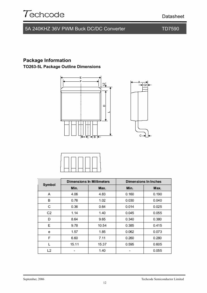
Package Information TO263-5L Package Outline Dimensions
Datasheet
5A 240KHZ 36V PWM Buck DC/DC Converter TD7590
September, 2006 Techcode Semiconductor Limited
13
Design Notes
Related Documents