FINAL Publication# 17502 Rev: D Amendment/+1 Issue Date: January 1998 Am28F020A 2 Megabit (256 K x 8-Bit) CMOS 12.0 Volt, Bulk Erase Flash Memory with Embedded Algorithms DISTINCTIVE CHARACTERISTICS ■ High performance — Access times as fast as 70 ns ■ CMOS low power consumption — 30 mA maximum active current — 100 μA maximum standby current — No data retention power consumption ■ Compatible with JEDEC-standard byte-wide 32-pin EPROM pinouts — 32-pin PDIP — 32-pin PLCC — 32-pin TSOP ■ 100,000 write/erase cycles minimum ■ Write and erase voltage 12.0 V ±5% ■ Latch-up protected to 100 mA from –1 V to V CC +1 V ■ Embedded Erase Electrical Bulk Chip Erase — Five seconds typical chip erase, including pre-programming ■ Embedded Program — 14 μs typical byte program, including time-out — 4 seconds typical chip program ■ Command register architecture for microprocessor/microcontroller compatible write interface ■ On-chip address and data latches ■ Advanced CMOS flash memory technology — Low cost single transistor memory cell ■ Embedded algorithms for completely self-timed write/erase operations GENERAL DESCRIPTION The Am28F020A is a 2 Megabit Flash memory orga- nized as 256 Kbytes of 8 bits each. AMD’s Flash mem- ories offer the most cost-effective and reliable read/ write non-volatile random access memory. The Am28F020A is packaged in 32-pin PDIP, PLCC, and TSOP versions. It is designed to be reprogrammed and erased in-system or in standard EPROM programmers. The Am28F020A is erased when shipped from the factory. The standard Am28F020A offers access times of as fast as 70 ns, allowing high speed microprocessors to operate without wait states. To eliminate bus conten- tion, the device has separate chip enable (CE#) and output enable (OE#) controls. AMD’s Flash memories augment EPROM functionality with in-circuit electrical erasure and programming. The Am28F020A uses a command register to manage this functionality. The command register allows for 100% TTL level control inputs and fixed power supply levels during erase and programming, while maintaining maximum EPROM compatibility. The Am28F020A is compatible with the AMD Am28F256A, Am28F512A, and Am28F010A Flash memories. All devices in the Am28Fxxx family follow the JEDEC 32-pin pinout standard. In addition, all devices within this family that offer Embedded Algo- rithms use the same command set. This offers designers the flexibility to retain the same device foot- print and command set, at any density between 256 Kbits and 2 Mbits. AMD’s Flash technology reliably stores memory con- tents even after 100,000 erase and program cycles. The AMD cell is designed to optimize the erase and programming mechanisms. In addition, the combina- tion of advanced tunnel oxide processing and low internal electric fields for erase and programming oper- ations produces reliable cycling. The Am28F020A uses a 12.0±5% V PP supply input to perform the erase and programming functions. The highest degree of latch-up protection is achieved with AMD’s proprietary non-epi process. Latch-up pro- tection is provided for stresses up to 100 mA on address and data pins from –1 V to V CC +1 V. AMD’s Flash technology combines years of EPROM and EEPROM experience to produce the highest levels of quality, reliability, and cost effectiveness. The Am28F020A electrically erases all bits simultaneously using Fowler-Nordheim tunneling. The bytes are programmed one byte at a time using the EPROM programming mechanism of hot electron injection.

Welcome message from author
This document is posted to help you gain knowledge. Please leave a comment to let me know what you think about it! Share it to your friends and learn new things together.
Transcript

FINAL
Publication# 17502 Rev: D Amendment/+1Issue Date: January 1998
Am28F020A2 Megabit (256 K x 8-Bit) CMOS 12.0 Volt, Bulk Erase Flash Memory with Embedded Algorithms
DISTINCTIVE CHARACTERISTICS High performance
— Access times as fast as 70 ns
CMOS low power consumption
— 30 mA maximum active current
— 100 µA maximum standby current
— No data retention power consumption
Compatible with JEDEC-standard byte-wide 32-pin EPROM pinouts
— 32-pin PDIP
— 32-pin PLCC
— 32-pin TSOP
100,000 write/erase cycles minimum Write and erase voltage 12.0 V ±5%
Latch-up protected to 100 mA from –1 V to VCC +1 V
Embedded Erase Electrical Bulk Chip Erase
— Five seconds typical chip erase, including pre-programming
Embedded Program
— 14 µs typical byte program, including time-out
— 4 seconds typical chip program
Command register architecture for microprocessor/microcontroller compatible write interface
On-chip address and data latches Advanced CMOS flash memory technology
— Low cost single transistor memory cell
Embedded algorithms for completely self-timed write/erase operations
GENERAL DESCRIPTIONThe Am28F020A is a 2 Megabit Flash memory orga-nized as 256 Kbytes of 8 bits each. AMD’s Flash mem-ories offer the most cost-effective and reliable read/write non-volat ile random access memory. TheAm28F020A is packaged in 32-pin PDIP, PLCC, andTSOP versions. It is designed to be reprogrammed anderased in-system or in standard EPROM programmers.The Am28F020A is erased when shipped fromthe factory.
The standard Am28F020A offers access times of asfast as 70 ns, allowing high speed microprocessors tooperate without wait states. To eliminate bus conten-tion, the device has separate chip enable (CE#) andoutput enable (OE#) controls.
AMD’s Flash memories augment EPROM functionalitywith in-circuit electrical erasure and programming. TheAm28F020A uses a command register to manage thisfunctionality. The command register allows for 100%TTL level control inputs and fixed power supply levelsduring erase and programming, while maintainingmaximum EPROM compatibility.
The Am28F020A is compatible wi th the AMDAm28F256A, Am28F512A, and Am28F010A Flashmemories. All devices in the Am28Fxxx family followthe JEDEC 32-pin pinout standard. In addition, all
devices within this family that offer Embedded Algo-r ithms use the same command set. This offersdesigners the flexibility to retain the same device foot-print and command set, at any density between256 Kbits and 2 Mbits.
AMD’s Flash technology reliably stores memory con-tents even after 100,000 erase and program cycles.The AMD cell is designed to optimize the erase andprogramming mechanisms. In addition, the combina-tion of advanced tunnel oxide processing and lowinternal electric fields for erase and programming oper-ations produces reliable cycling. The Am28F020A usesa 12.0±5% VPP supply input to perform the erase andprogramming functions.
The highest degree of latch-up protection is achievedwith AMD’s proprietary non-epi process. Latch-up pro-tection is provided for stresses up to 100 mA onaddress and data pins from –1 V to VCC +1 V.
AMD’s Flash technology combines years of EPROMand EEPROM experience to produce the highest levelsof quality, reliability, and cost effectiveness. TheAm28F020A electrically erases all bits simultaneouslyusing Fowler-Nordheim tunneling. The bytes areprogrammed one byte at a time using the EPROMprogramming mechanism of hot electron injection.
Embedded ProgramThe Am28F020A is byte programmable using theEmbedded Program algorithm, which does not requirethe system to time-out or verify the data programmed.The typical room temperature programming time of thisdevice is four seconds.
Embedded EraseThe entire device is bulk erased using the EmbeddedErase algorithm, which automatically programs theentire array prior to electrical erase. The timing and ver-ification of electrical erase are controlled internal to thedevice. Typical erasure time at room temperature is fiveseconds, including preprogramming.
Commands are written to the command register usingstandard microprocessor write timings. Register con-tents serve as input to an internal state-machine,which controls the erase and programming circuitry.During write cycles, the command register internallylatches addresses and data needed for the program-ming and erase operations. For system designsimplification, the Am28F010A is designed to support
either WE# or CE# controlled writes. During a systemwrite cycle, addresses are latched on the falling edgeof WE# or CE#, whichever occurs last. Data is latchedon the rising edge of WE# or CE#, whichever occursfirst. To simplify the following discussion, the WE# pinis used as the write cycle control pin throughout therest of this text. All setup and hold times are withrespect to the WE# signal.
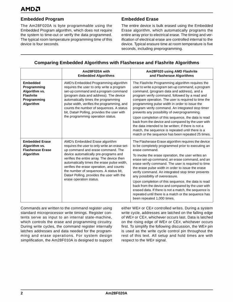
Comparing Embedded Algorithms with Flasherase and Flashrite Algorithms
Am28F020A with Embedded Algorithms
Am28F020 using AMD Flashrite and Flasherase Algorithms
Embedded Programming Algorithm vs. Flashrite Programming Algorithm
AMD’s Embedded Programming algorithm requires the user to only write a program set-up command and a program command (program data and address). The device automatically times the programming pulse width, verifies the programming, and counts the number of sequences. A status bit, Data# Polling, provides the user with the programming operation status.
The Flashrite Programming algorithm requires the user to write a program set-up command, a program command, (program data and address), and a program verify command, followed by a read and compare operation. The user is required to time the programming pulse width in order to issue the program verify command. An integrated stop timer prevents any possibility of overprogramming.
Upon completion of this sequence, the data is read back from the device and compared by the user with the data intended to be written; if there is not a match, the sequence is repeated until there is a match or the sequence has been repeated 25 times.
Embedded Erase Algorithm vs. Flasherase Erase Algorithm
AMD’s Embedded Erase algorithm requires the user to only write an erase set-up command and erase command. The device automatically pre-programs and verifies the entire array. The device then automatically times the erase pulse width, verifies the erase operation, and counts the number of sequences. A status bit, Data# Polling, provides the user with the erase operation status.
The Flasherase Erase algorithm requires the device to be completely programmed prior to executing an erase command.
To invoke the erase operation, the user writes an erase set-up command, an erase command, and an erase verify command. The user is required to time the erase pulse width in order to issue the erase verify command. An integrated stop timer prevents any possibility of overerasure.
Upon completion of this sequence, the data is read back from the device and compared by the user with erased data. If there is not a match, the sequence is repeated until there is a match or the sequence has been repeated 1,000 times.
2 Am28F020A

PRODUCT SELECTOR GUIDE
BLOCK DIAGRAM
Family Part Number Am28F020A
Speed Options (VCC = 5.0 V ± 10%) -70 -90 -120 -150 -200
Max Access Time (ns) 70 90 120 150 200
CE# (E#) Access (ns) 70 90 120 150 200
OE# (G#) Access (ns) 35 35 50 55 55
17502D-1
Erase VoltageSwitch
Input/OutputBuffers
Data Latch
Y-Gating
2,097,152Bit
Cell Matrix
X-Decoder
Y-Decoder
Chip EnableOutput Enable
Logic
Program/ErasePulse Timer
Low VCC Detector
CommandRegister
WE#
CE#OE#
A0–A17
DQ0–DQ7VCCVSS
Add
ress
Lat
ch
StateControl
VPP
To Array
ProgramVoltageSwitch
EmbeddedAlgorithms
Am28F020A 3

CONNECTION DIAGRAMS
Note : Pin 1 is marked for orientation.
3
4
5
2
1
9
10
11
12
13
27
26
25
24
23
7
8
22
21
6
32
31
20
14
30
29
28
15
16
19
18
17
A6
A5
A4
A3
A2
A1
A0
A16
DQ0
A15
A12
A7
DQ1
DQ2
VSS
A8
A9
A11
OE# (G#)
A10
CE# (E#)
DQ7
VCC
WE# (W#)
DQ6
A17
A14
A13
DQ5
DQ4
DQ3
VPP
17502D-2
PDIP
1 31 30234
5
6
7
8
9
10
11
12
13
17 18 19 20161514
29
28
27
26
25
24
23
22
21
32
A7
A6
A5
A4
A3
A2
A1
A0
DQ0
A14
A13
A8
A9
A11
OE# (G#)
A10
CE# (E#)
DQ7
A12
A15
A16
VP
PV
CC
WE
# (W
#)
A17
DQ
1D
Q2
VS
S
DQ
3
DQ
4
DQ
5
DQ
6
PLCC
17502D-3
4 Am28F020A

CONNECTION DIAGRAMS (Continued)
LOGIC SYMBOL
12345678910111213141516
32-Pin TSOP—Standard Pinout
A11A9A8
A13A14A17
WE#VCCVPPA16A15A12
A7A6A5A4
32313029282726252423222120191817
OE#A10CE#D7D6D5D4D3VSSD2D1D0A0A1A2A3
32-Pin TSOP—Reverse Pinout
12345678910111213141516
A11A9A8A13A14A17WE#VCCVPPA16A15A12A7A6A5A4
32313029282726252423222120191817
OE#A10CE#
D7D6D5D4D3
VSSD2D1D0A0A1A2A3
17502D-4
18
8
DQ0–DQ7
A0–A17
CE# (E#)
OE# (G#)
WE# (W#)
17502D-5
Am28F020A 5
ORDERING INFORMATION
Standard Products
AMD standard products are available in several packages and operating ranges. The ordering number (Valid Combination) isformed by a combination of the following:
Valid Combinations
Valid Combinations list configurations planned to be support-ed in volume for this device. Consult the local AMD sales of-fice to confirm availability of specific valid combinations andto check on newly released combinations.
DEVICE NUMBER/DESCRIPTIONAm28F020A 2 Megabit (256 K x 8-Bit) CMOS Flash Memory with Embedded Algorithms
AM28F020A -70 J C
OPTIONAL PROCESSINGBlank = Standard ProcessingB = Burn-In
Contact an AMD representative for more information.
TEMPERATURE RANGEC = Commercial (0°C to +70°C)I = Industrial (–40°C to +85°C)E = Extended (–55°C to +125°C)
PACKAGE TYPEP = 32-Pin Plastic DIP (PD 032)J = 32-Pin Rectangular Plastic Leaded Chip
Carrier (PL 032)E = 32-Pin Thin Small Outline Package (TSOP)
Standard Pinout (TS 032)F = 32-Pin Thin Small Outline Package (TSOP)
Reverse Pinout (TSR032)
SPEED OPTIONSee Product Selector Guide and Valid Combinations
B
Valid Combinations
AM28F020A-70
PC, PI, PE,JC, JI, JE, EC, EI, EE, FC, FI, FE
AM28F020A-90
AM28F020A-120
AM28F020A-150
AM28F020A-200
6 Am28F020A

PIN DESCRIPTION
A0–A17Address Inputs for memory locations. Internal latcheshold addresses during write cycles.
CE# (E#)Chip Enable active low input activates the chip’s controllogic and input buffers. Chip Enable high will deselectthe device and operates the chip in stand-by mode.
DQ0–DQ7Data Inputs during memory write cycles. Internallatches hold data during write cycles. Data Outputsduring memory read cycles.
NCNo Connect-corresponding pin is not connected inter-nally to the die.
OE# (G#)Output Enable active low input gates the outputs ofthe device through the data buffers during memoryread cycles. Output Enable is high during commandsequencing and program/erase operations.
VPPProgram voltage input. VPP must be at high voltage inorder to write to the command register. The commandregister controls all functions required to alter the mem-ory array contents. Memory contents cannot be alteredwhen VPP ≤ VCC +2 V.
VCC
Power supply for device operation. (5.0 V ± 5% or 10%)
VSSGround.
WE# (W#)Write Enable active low input controls the write functionof the command register to the memory array. The tar-get address is latched on the falling edge of the WriteEnable pulse and the appropriate data is latched on therising edge of the pulse. Write Enable high inhibits writ-ing to the device.
Am28F020A 7
BASIC PRINCIPLESThe Am28FxxxA family uses 100% TTL-level controlinputs to manage the command register. Erase andreprogramming operations use a fixed 12.0 V ± 5%high voltage input.
Read Only MemoryWithout high VPP voltage, the device functions as aread only memory and operates like a standardEPROM. The control inputs still manage traditionalread, standby, output disable, and Auto select modes.
Command RegisterThe command register is enabled only when high volt-age is applied to the VPP pin. The erase and repro-gramming operations are only accessed via theregister. In addition, two-cycle commands are requiredfor erase and reprogramming operations. The tradi-tional read, standby, output disable, and Auto selectmodes are available via the register.
The device’s command register is written using standardmicroprocessor write timings. The register controls aninternal state machine that manages all device opera-tions. For system design simplification, the device is de-signed to support either WE# or CE# controlled writes.During a system write cycle, addresses are latched onthe falling edge of WE# or CE# whichever occurs last.Data is latched on the rising edge of WE# or CE# which-ever occur first. To simplify the following discussion, theWE# pin is used as the write cycle control pin throughoutthe rest of this text. All setup and hold times are with re-spect to the WE# signal.
OVERVIEW OF ERASE/PROGRAM OPERATIONS
Embedded Erase AlgorithmAMD now makes erasure extremely simple and reli-able. The Embedded Erase algorithm requires the userto only write an erase setup command and erase com-mand. The device will automatically pre-program andverify the entire array. The device automatically timesthe erase pulse width, provides the erase verify andcounts the number of sequences. A status bit, Data#Polling, provides feedback to the user as to the statusof the erase operation.
Embedded Programming AlgorithmAMD now makes programming extremely simple andreliable. The Embedded Programming algorithm re-
quires the user to only write a program setup commandand a program command. The device automaticallytimes the programming pulse width, provides the pro-gram verify and counts the number of sequences. Astatus bit, Data# Polling, provides feedback to the useras to the status of the programming operation.
DATA PROTECTIONThe device is designed to offer protection against acci-dental erasure or programming caused by spurioussystem level signals that may exist during power transi-tions. The device powers up in its read only state. Also,with its control register architecture, alteration of thememory contents only occurs after successful comple-tion of specific command sequences.
The device also incorporates several features to pre-vent inadver tent write cycles resulting from VCCpower-up and power-down transitions or system noise.
Low V CC Write InhibitTo avoid initiation of a write cycle during VCC power-upand power-down, the device locks out write cycles forVCC < VLKO (see DC characteristics section for volt-ages). When VCC < VLKO, the command register is dis-abled, all internal program/erase circuits are disabled,and the device resets to the read mode. The device ig-nores all writes until VCC > VLKO. The user must ensurethat the control pins are in the correct logic state whenVCC > VLKO to prevent unintentional writes.
Write Pulse “Glitch” ProtectionNoise pulses of less than 10 ns (typical) on OE#, CE#or WE# will not initiate a write cycle.
Logical InhibitWriting is inhibited by holding any one of OE# = VIL,CE#=VIH or WE# = VIH. To initiate a write cycle CE#and WE# must be a logical zero while OE# is a logicalone.
Power-Up Write InhibitPower-up of the device with WE# = CE# = VIL andOE# = VIH will not accept commands on the risingedge of WE#. The internal state machine is automati-cally reset to the read mode on power-up.
8 Am28F020A

FUNCTIONAL DESCRIPTION
Description Of User ModesTable 1. Am28F020A Device Bus Operations (Notes 7 and 8)
Legend:X = Don’t care, where Don’t Care is either VIL or VIH levels. VPPL = VPP < VCC + 2 V. See DC Characteristics for voltage levels
of VPPH. 0 V < An < VCC + 2 V, (normal TTL or CMOS input levels, where n = 0 or 9).
Notes:1. VPPL may be grounded, connected with a resistor to ground, or < VCC + 2.0 V. VPPH is the programming voltage specified for
the device. Refer to the DC characteristics. When VPP = VPPL, memory contents can be read but not written or erased.2. Manufacturer and device codes may also be accessed via a command register write sequence. Refer to Table 2.3. 11.5 < VID < 13.0 V. Minimum VID rise time and fall time (between 0 and VID voltages) is 500 ns.4. Read operation with VPP = VPPH may access array data or the Auto select codes.5. With VPP at high voltage, the standby current is ICC + IPP (standby).6. Refer to Table 3 for valid DIN during a write operation.7. All inputs are Don’t Care unless otherwise stated, where Don’t Care is either VIL or VIH levels. In the Auto select mode all
addresses except A9 and A0 must be held at VIL.8. If VCC ≤ 1.0 Volt, the voltage difference between VPP and VCC should not exceed 10.0 volts. Also, the Am28F256 has a VPP
rise time and fall time specification of 500 ns minimum.
OperationCE#(E#)
OE#(G#)
WE#(W#)
VPP(Note 1) A0 A9 I/O
Read-Only
Read VIL VIL X VPPL A0 A9 DOUT
Standby VIH X X VPPL X X HIGH Z
Output Disable VIL VIH VIH VPPL X X HIGH Z
Auto-select ManufacturerCode (Note 2)
VIL VIL VIH VPPL VILVID
(Note 3)CODE(01h)
Auto-select DeviceCode (Note 2)
VIL VIL VIH VPPL VIHVID
(Note 3)CODE(29h)
Read/Write
Read VIL VIL VIH VPPH A0 A9 DOUT(Note 4)
Standby (Note 5) VIH X X VPPH X X HIGH Z
Output Disable VIL VIH VIH VPPH X X HIGH Z
Write VIL VIH VIL VPPH A0 A9 DIN(Note 6)
Am28F020A 9

READ-ONLY MODEWhen VPP is less than VCC + 2 V, the command registeris inactive. The device can either read array or autose-lect data, or be standby mode.
ReadThe device functions as a read only memory when VPP< VCC + 2 V. The device has two control functions. Bothmust be satisfied in order to output data. CE# controlspower to the device. This pin should be used for spe-cific device selection. OE# controls the device outputsand should be used to gate data to the output pins if adevice is selected.
Address access time tACC is equal to the delay fromstable addresses to valid output data. The chip enableaccess time tCE is the delay from stable addresses andstable CE# to valid data at the output pins. The outputenable access time is the delay from the falling edge ofOE# to valid data at the output pins (assuming the ad-dresses have been stable at least tACC - tOE).
Standby ModeThe device has two standby modes. The CMOSstandby mode (CE# input held at VCC ± 0.5 V), con-sumes less than 100 µA of current. TTL standby mode(CE# is held at VIH) reduces the current requirementsto less than 1 mA. When in the standby mode the out-puts are in a high impedance state, independent of theOE# input.
If the device is deselected during erasure, program-ming, or program/erase verification, the device willdraw active current until the operation is terminated.
Output DisableOutput from the device is disabled when OE# is at alogic high level. When disabled, output pins are in ahigh impedance state.
Auto SelectFlash memories can be programmed in-system or in astandard PROM programmer. The device may be sol-dered to the circuit board upon receipt of shipment andprogrammed in-system. Alternatively, the device mayinitially be programmed in a PROM programmer priorto soldering the device to the board.
The Auto select mode allows the reading out of a binarycode from the device that will identify its manufacturer andtype. This mode is intended for the purpose of automati-cally matching the device to be programmed with its cor-responding programming algorithm. This mode isfunctional over the entire temperature range of the device.
Programming In A PROM ProgrammerTo activate this mode, the programming equipmentmust force VID (11.5 V to 13.0 V) on address A9. Twoidentifier bytes may then be sequenced from the deviceoutputs by toggling address A0 from VIL to VIH. All otheraddress lines must be held at VIL, and VPP must beless than or equal to VCC + 2.0 V while using this Autoselect mode. Byte 0 (A0 = VIL) represents the manufac-turer code and byte 1 (A0 = VIH) the device identifiercode. For the device the two bytes are given in the table2 of the device data sheet. All identifiers for manufac-turer and device codes will exhibit odd parity with theMSB (DQ7) defined as the parity bit.
Table 2. (Am28F020A Auto Select Code
Type A0Code(HEX)
Manufacturer Code VIL 01
Device Code VIH 29
10 Am28F020A

ERASE, PROGRAM, AND READ MODEWhen VPP is equal to 12.0 V ± 5%, the command reg-ister is active. All functions are available. That is, thedevice can program, erase, read array or autoselectdata, or be standby mode.
Write OperationsHigh voltage must be applied to the VPP pin in order toactivate the command register. Data written to the reg-ister serves as input to the internal state machine. Theoutput of the state machine determines the operationalfunction of the device.
The command register does not occupy an address-able memory location. The register is a latch that storesthe command, along with the address and data infor-mation needed to execute the command. The registeris written by bringing WE# and CE# to VIL, while OE#is at VIH. Addresses are latched on the falling edge ofWE#, while data is latched on the rising edge of theWE# pulse. Standard microprocessor write timings areused.
The device requires the OE# pin to be VIH for write op-erations. This condition eliminates the possibility forbus contention during programming operations. Inorder to write, OE# must be VIH, and CE# and WE#must be VIL. If any pin is not in the correct state a writecommand will not be executed.
Refer to AC Write Characteristics and the Erase/Pro-gramming Waveforms for specific timing parameters.
Command Definitions The contents of the command register default to 00h(Read Mode) in the absence of high voltage applied tothe VPP pin. The device operates as a read onlymemory. High voltage on the VPP pin enables thecommand register. Device operations are selected bywriting specific data codes into the command register.Table 3 in the device data sheet defines these registercommands.
Read CommandMemory contents can be accessed via the read com-mand when VPP is high. To read from the device, write00h into the command register. Standard microproces-sor read cycles access data from the memory. The de-vice will remain in the read mode until the commandregister contents are altered.
The command register defaults to 00h (read mode)upon VPP power-up. The 00h (Read Mode) register de-fault helps ensure that inadvertent alteration of thememory contents does not occur during the VPP powertransition. Refer to the AC Read Characteristics andWaveforms for the specific timing parameters.
Table 3. Am28F020A Command Definitions
Notes:1. Bus operations are defined in Table 1.
2. RA = Address of the memory location to be read.PA = Address of the memory location to be programmed.Addresses are latched on the falling edge of the WE# pulse.X = Don’t care.
3. RD = Data read from location RA during read operation.PD = Data to be programmed at location PA. Data latched on the rising edge of WE#.
4. Please reference Reset Command section.
Command
First Bus Cycle Second Bus Cycle
Operation (Note 1)
Address (Note 2)
Data (Note 3)
Operation (Note 1)
Address Note 2)
Data (Note 3)
Read Memory (Note 4) Write X 00h/FFh Read RA RD
Read Auto select Write X 80h or 90h Read 00h/01h 01h/29h
Embedded Erase Set-up/Embedded Erase
Write X 30h Write X 30h
Embedded Program Set-up/Embedded Program
Write X 10h or 50h Write PA PD
Reset (Note 4) Write X 00h/FFh Write X 00h/FFh
Am28F020A 11
FLASH MEMORY PROGRAM/ERASEOPERATIONS
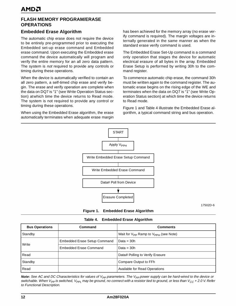
Embedded Erase AlgorithmThe automatic chip erase does not require the deviceto be entirely pre-programmed prior to executing theEmbedded set-up erase command and Embeddederase command. Upon executing the Embedded erasecommand the device automatically will program andverify the entire memory for an all zero data pattern.The system is not required to provide any controls ortiming during these operations.
When the device is automatically verified to contain anall zero pattern, a self-timed chip erase and verify be-gin. The erase and verify operation are complete whenthe data on DQ7 is “1" (see Write Operation Status sec-tion) atwhich time the device returns to Read mode.The system is not required to provide any control ortiming during these operations.
When using the Embedded Erase algorithm, the eraseautomatically terminates when adequate erase margin
has been achieved for the memory array (no erase ver-ify command is required). The margin voltages are in-ternally generated in the same manner as when thestandard erase verify command is used.
The Embedded Erase Set-Up command is a commandonly operation that stages the device for automaticelectrical erasure of all bytes in the array. EmbeddedErase Setup is performed by writing 30h to the com-mand register.
To commence automatic chip erase, the command 30hmust be written again to the command register. The au-tomatic erase begins on the rising edge of the WE andterminates when the data on DQ7 is “1" (see Write Op-eration Status section) at which time the device returnsto Read mode.
Figure 1 and Table 4 illustrate the Embedded Erase al-gorithm, a typical command string and bus operation.
Table 4. Embedded Erase Algorithm
Note: See AC and DC Characteristics for values of VPP parameters. The VPP power supply can be hard-wired to the device or switchable. When VPP is switched, VPPL may be ground, no connect with a resistor tied to ground, or less than VCC + 2.0 V. Refer to Functional Description.
Bus Operations Command Comments
Standby Wait for VPP Ramp to VPPH (see Note)
WriteEmbedded Erase Setup Command Data = 30h
Embedded Erase Command Data = 30h
Read Data# Polling to Verify Erasure
Standby Compare Output to FFh
Read Available for Read Operations
START
Apply VPPH
Erasure Completed
Data# Poll from Device
Write Embedded Erase Command
Write Embedded Erase Setup Command
17502D-6
Figure 1. Embedded Erase Algorithm
12 Am28F020A

Embedded Programming AlgorithmThe Embedded Program Setup is a command only op-eration that stages the device for automatic program-ming. Embedded Program Setup is performed bywriting 10h or 50h to the command register.
Once the Embedded Setup Program operation is per-formed, the next WE# pulse causes a transition to anactive programming operation. Addresses are latchedon the falling edge of CE# or WE# pulse, whicheverhappens later. Data is latched on the rising edge ofWE# or CE#, whichever happens first. The rising edge
of WE# also begins the programming operation. Thesystem is not required to provide further controls ortimings. The device will automatically provide an ade-quate internally generated program pulse and verifymargin. The automatic programming operation iscompleted when the data on DQ7 is equivalent to datawritten to this bit (see Write Operation Status section)at which time the device returns to Read mode.
Figure 2 and Table 5 illustrate the Embedded Programalgorithm, a typical command string, and bus operation.
Table 5. Embedded Programming Algorithm
Note: See AC and DC Characteristics for values of VPP parameters. The VPP power supply can be hard-wired to the device or switchable. When VPP is switched, VPPL may be ground, no connect with a resistor tied to ground, or less than VCC + 2.0 V. Refer to Functional Description. Device is either powered-down, erase inhibit or program inhibit.
Bus Operations Command Comments
Standby Wait for VPP Ramp to VPPH (see Note)
Write Embedded Program Setup Command Data = 10h or 50h
Write Embedded Program Command Valid Address/Data
Read Data# Polling to Verify Completion
Read Available for Read Operations
START
Apply VPPH
Write Embedded Setup Program Command
Write Embedded Program Command (A/D)
Programming Completed
Yes
Data# Poll Device
Increment AddressNo
17502D-7
Figure 2. Embedded Programming Algorithm
Last Address
Am28F020A 13

Write Operation StatusData Polling—DQ7
The device features Data# Polling as a method to indi-cate to the host system that the Embedded algorithmsare either in progress or completed.
While the Embedded Programming algorithm is in oper-ation, an attempt to read the device at a valid addresswill produce the complement of expected Valid data onDQ7. Upon completion of the Embedded Program algo-rithm an attempt to read the device at a valid address willproduce Valid data on DQ7. The Data# Polling feature isvalid after the rising edge of the second WE# pulse ofthe two write pulse sequence.
While the Embedded Erase algorithm is in operation,DQ7 will read “0" until the erase operation is com-pleted. Upon completion of the erase operation, thedata on DQ7 will read “1.” The Data# Polling feature isvalid after the rising edge of the second WE# pulse ofthe two Write pulse sequence.
The Data# Polling feature is only active during Embed-ded Programming or erase algorithms.
See Figures 3 and 4 for the Data# Polling timing spec-ifications and diagrams. Data# Polling is the standardmethod to check the write operation status, however,an alternative method is available using Toggle Bit.
START
Fail
No
DQ7 = Data?
DQ7 = Data?
DQ5 = 1?
No
Pass
Yes
No
Yes
Read Byte(DQ0–DQ7)Addr = VA
Read Byte(DQ0–DQ7)Addr = VA
Yes
VA = Byte address for programming= XXXXh during chip erase
17502D-8
Note:DQ7 is rechecked even if DQ5 = “1” because DQ7 may change simultaneously with DQ5 or after DQ5.
Figure 3. Data # Polling Algorithm
14 Am28F020A

tCH
tOEH
tOE
tCE
tWHWH 3 or 4
DQ7# DQ7 = Valid Data
High Z
CE#
OE#
WE#
DQ7
tOH
tDF
DQ0–DQ6 = InvalidDQ0–DQ6 DQ0–DQ7Valid Data
*
17502D-9
*DQ7 = Valid Data (The device has completed the Embedded operation.)
Figure 4. AC Waveforms for Data # Polling during Embedded Algorithm Operations
Am28F020A 15
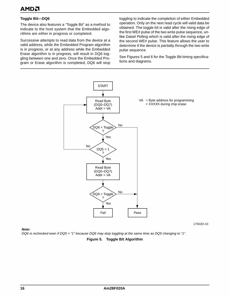
Toggle Bit—DQ6
The device also features a “Toggle Bit” as a method toindicate to the host system that the Embedded algo-rithms are either in progress or completed.
Successive attempts to read data from the device at avalid address, while the Embedded Program algorithmis in progress, or at any address while the EmbeddedErase algorithm is in progress, will result in DQ6 tog-gling between one and zero. Once the Embedded Pro-gram or Erase algorithm is completed, DQ6 will stop
toggling to indicate the completion of either Embeddedoperation. Only on the next read cycle will valid data beobtained. The toggle bit is valid after the rising edge ofthe first WE# pulse of the two write pulse sequence, un-like Data# Polling which is valid after the rising edge ofthe second WE# pulse. This feature allows the user todetermine if the device is partially through the two writepulse sequence.
See Figures 5 and 6 for the Toggle Bit timing specifica-tions and diagrams.
START
Fail
NoDQ6 = Toggle
?
DQ5 = 1?
Pass
Yes
No
Read Byte(DQ0–DQ7)Addr = VA
Read Byte(DQ0–DQ7)Addr = VA
Yes
No
Yes
DQ6 = Toggle?
VA = Byte address for programming= XXXXh during chip erase
17502D-10
Note:DQ6 is rechecked even if DQ5 = “1” because DQ6 may stop toggling at the same time as DQ5 changing to “1”.
Figure 5. Toggle Bit Algorithm
16 Am28F020A

DQ5Exceeded Timing Limits
DQ5 will indicate if the program or erase time hasexceeded the specified limits. This is a failure condi-tion and the device may not be used again (internalpulse count exceeded). Under these conditions DQ5will produce a “1.” The program or erase cycle was notsuccessfully completed. Data# Polling is the only op-erating function of the device under this condition. TheCE# circuit will partially power down the device underthese conditions (to approximately 2 mA). The OE#and WE# pins will control the output disable functionsas described in the Command Definitions table in thecorresponding device data sheet.
Parallel Device Erasure
The Embedded Erase algorithm greatly simplifies par-allel device erasure. Since the erase process is internalto the device, a single erase command can be given tomultiple devices concurrently. By implementing a paral-lel erase algorithm, total erase time may be minimized.
Note that the Flash memories may erase at differentrates. If this is the case, when a device is completelyerased, use a masking code to prevent further erasure(over-erasure). The other devices will continue to eraseuntil verified. The masking code applied could be theread command (00h).
Power-Up/Power-Down Sequence
The device powers-up in the Read only mode. Powersupply sequencing is not required. Note that if VCC ≤1.0 Volt, the voltage difference between VPP and VCCshould not exceed 10.0 Volts. Also, the device has arise VPP rise time and fall time specification of 500 nsminimum.
Reset Command
The Reset command initializes the Flash memory de-vice to the Read mode. In addition, it also provides theuser with a safe method to abort any device operation(including program or erase).
The Reset must be written two consecutive times afterthe Setup Program command (10h or 50h). This willreset the device to the Read mode.
Following any other Flash command, write the Resetcommand once to the device. This will safely abort anyprevious operation and initialize the device to the Readmode.
The Setup Program command (10h or 50h) is the onlycommand that requires a two-sequence reset cycle. Thefirst Reset command is interpreted as program data.However, FFh data is considered as null data during pro-gramming operations (memory cells are only pro-grammed from a logical “1" to “0"). The second Resetcommand safely aborts the programming operation andresets the device to the Read mode.
Memory contents are not altered in any case.
CE#
tOEH
WE#
OE#
DataDQ0–DQ7
DQ6 = DQ6 = DQ6Stop Toggling
DQ0–DQ7Valid
tOE
*
17502D-11
Note:
*DQ6 stops toggling (The device has completed the Embedded operation.)
Figure 6. AC Waveforms for Toggle Bit during Embedded Algorithm Operations
Am28F020A 17
This detailed information is for your reference. It mayprove easier to always issue the Reset command twoconsecutive times. This eliminates the need to deter-mine if you are in the Setup Program state or not.
In-System Programming Considerations
Flash memories can be programmed in-system or in astandard PROM programmer. The device may be sol-dered to the circuit board upon receipt of shipment andprogrammed in-system. Alternatively, the device mayinitially be programmed in a PROM programmer priorto soldering the device to the circuit board.
Auto Select Command
AMD’s Flash memories are designed for use in appli-cations where the local CPU alters memory contents.In order to correctly program any Flash memories
in-system, manufacturer and device codes must beaccessible while the device resides in the targetsystem. PROM programmers typically access the sig-nature codes by raising A9 to a high voltage. However,multiplexing high voltage onto address lines is not agenerally desired system design practice.
The device contains an Auto Select operation to supple-ment traditional PROM programming methodologies.The operation is initiated by writing 80h or 90h into thecommand register. Following this command, a readcycle address 0000h retrieves the manufacturer code of01h (AMD). A read cycle from address 0001h returnsthe device code (see the Auto Select Code table of thecorresponding device data sheet). To terminate the op-eration, it is necessary to write another valid command,such as Reset (00h or FFh), into the register.
18 Am28F020A

ABSOLUTE MAXIMUM RATINGSStorage Temperature . . . . . . . . . . . . –65°C to +125°CAmbient Temperaturewith Power Applied. . . . . . . . . . . . . . –55°C to +125°CVoltage with Respect to GroundAll pins except A9 and VPP (Note 1) .–2.0 V to +7.0 V
VCC (Note 1). . . . . . . . . . . . . . . . . . . .–2.0 V to +7.0 V
A9, VPP (Note 2) . . . . . . . . . . . . . . .–2.0 V to +14.0 V
Output Short Circuit Current (Note 3) . . . . . . 200 mA
Notes:1. Minimum DC voltage on input or I/O pins is –0.5 V. During
voltage transitions, input or I/O pins may overshoot VSS to –2.0 V for periods of up to 20 ns. Maximum DC voltage on input or I/O pins is VCC +0.5 V. During voltage transitions, input or I/O pins may overshoot to VCC +2.0 V for periods up to 20 ns.
2. Minimum DC input voltage on pins A9 and VPP is –0.5 V. During voltage transitions, A9 and VPP may overshoot VSS to –2.0 V for periods of up to 20 ns. Maximum DC input voltage on pin A9 and VPP is +13.0 V, which may overshoot to 14.0 V for periods up to 20 ns.
3. No more than one output may be shorted to ground at a time. Duration of the short circuit should not be greater than one second.
4. Stresses above those listed under “Absolute Maximum Ratings” may cause permanent damage to the device. This is a stress rating only; functional operation of the device at these or any other conditions above those indicated in the operational sections of this data sheet is not implied. Exposure of the device to absolute maximum rating conditions for extended periods may affect device reliability.
OPERATING RANGESCommercial (C) Devices
Ambient Temperature (TA). . . . . . . . . . . .0°C to +70°C
Industrial (I) Devices
Ambient Temperature (TA). . . . . . . . . .–40°C to +85°C
Extended (E) Devices
Ambient Temperature (TA). . . . . . . . .–55°C to +125°C
VCC Supply Voltages
VCC . . . . . . . . . . . . . . . . . . . . . . . . +4.50 V to +5.50 V
VPP Voltages
Read . . . . . . . . . . . . . . . . . . . . . . . . –0.5 V to +12.6 V
Program, Erase, and Verify . . . . . . +11.4 V to +12.6 V
Operating ranges define those limits between which thefunctionality of the device is guaranteed.
Am28F020A 19
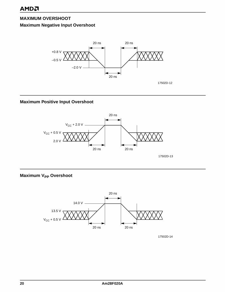
MAXIMUM OVERSHOOT
Maximum Negative Input Overshoot
Maximum Positive Input Overshoot
Maximum V PP Overshoot
20 ns
20 ns
+0.8 V
–0.5 V
20 ns
–2.0 V
17502D-12
20 ns
VCC + 0.5 V
2.0 V
20 ns 20 ns
VCC + 2.0 V
17502D-13
17502D-14
20 ns
13.5 V
VCC + 0.5 V
20 ns 20 ns
14.0 V
20 Am28F020A
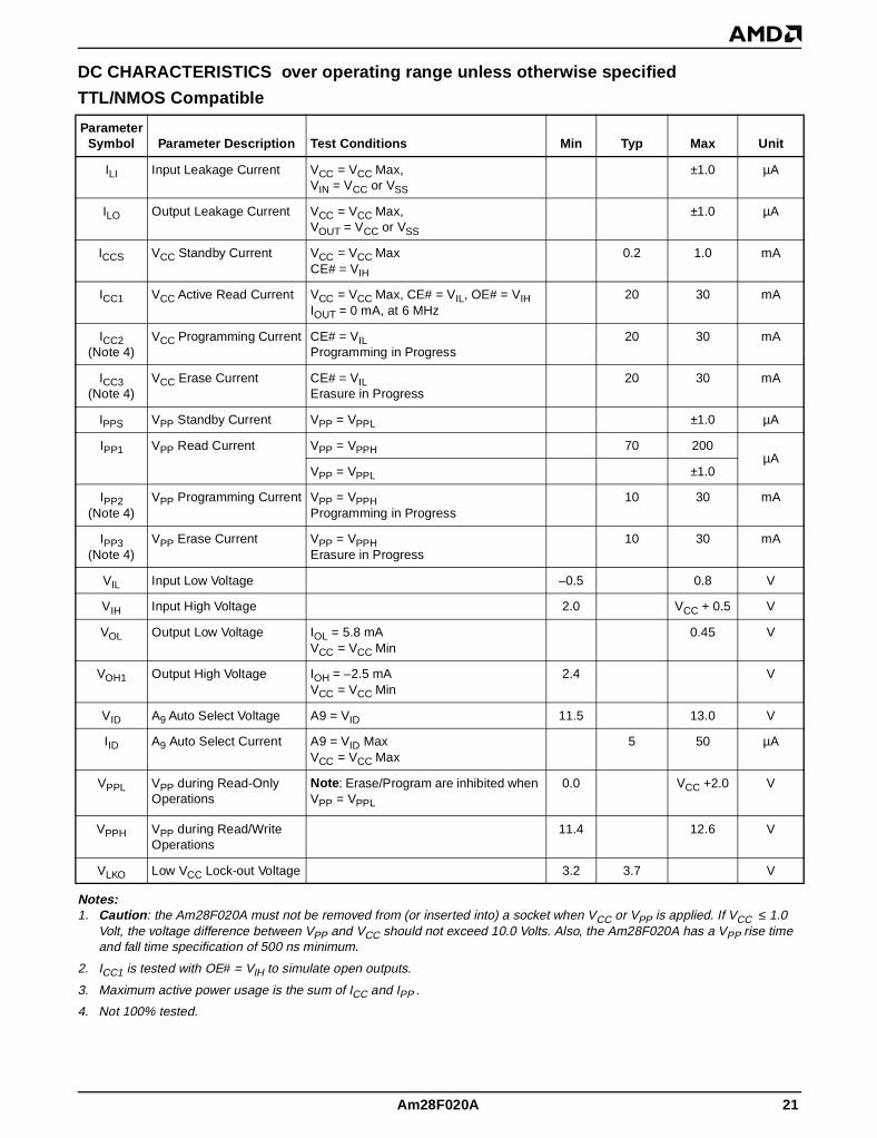
DC CHARACTERISTICS over operating range unless otherwise specified
TTL/NMOS Compatible
Notes:1. Caution : the Am28F020A must not be removed from (or inserted into) a socket when VCC or VPP is applied. If VCC ≤ 1.0
Volt, the voltage difference between VPP and VCC should not exceed 10.0 Volts. Also, the Am28F020A has a VPP rise time and fall time specification of 500 ns minimum.
2. ICC1 is tested with OE# = VIH to simulate open outputs.
3. Maximum active power usage is the sum of ICC and IPP .
4. Not 100% tested.
Parameter Symbol Parameter Description Test Conditions Min Typ Max Unit
ILI Input Leakage Current VCC = VCC Max, VIN = VCC or VSS
±1.0 µA
ILO Output Leakage Current VCC = VCC Max,VOUT = VCC or VSS
±1.0 µA
ICCS VCC Standby Current VCC = VCC MaxCE# = VIH
0.2 1.0 mA
ICC1 VCC Active Read Current VCC = VCC Max, CE# = VIL, OE# = VIHIOUT = 0 mA, at 6 MHz
20 30 mA
ICC2(Note 4)
VCC Programming Current CE# = VILProgramming in Progress
20 30 mA
ICC3(Note 4)
VCC Erase Current CE# = VILErasure in Progress
20 30 mA
IPPS VPP Standby Current VPP = VPPL ±1.0 µA
IPP1 VPP Read Current VPP = VPPH 70 200µA
VPP = VPPL ±1.0
IPP2(Note 4)
VPP Programming Current VPP = VPPHProgramming in Progress
10 30 mA
IPP3(Note 4)
VPP Erase Current VPP = VPPHErasure in Progress
10 30 mA
VIL Input Low Voltage –0.5 0.8 V
VIH Input High Voltage 2.0 VCC + 0.5 V
VOL Output Low Voltage IOL = 5.8 mAVCC = VCC Min
0.45 V
VOH1 Output High Voltage IOH = –2.5 mAVCC = VCC Min
2.4 V
VID A9 Auto Select Voltage A9 = VID 11.5 13.0 V
IID A9 Auto Select Current A9 = VID MaxVCC = VCC Max
5 50 µA
VPPL VPP during Read-Only Operations
Note: Erase/Program are inhibited when VPP = VPPL
0.0 VCC +2.0 V
VPPH VPP during Read/Write Operations
11.4 12.6 V
VLKO Low VCC Lock-out Voltage 3.2 3.7 V
Am28F020A 21
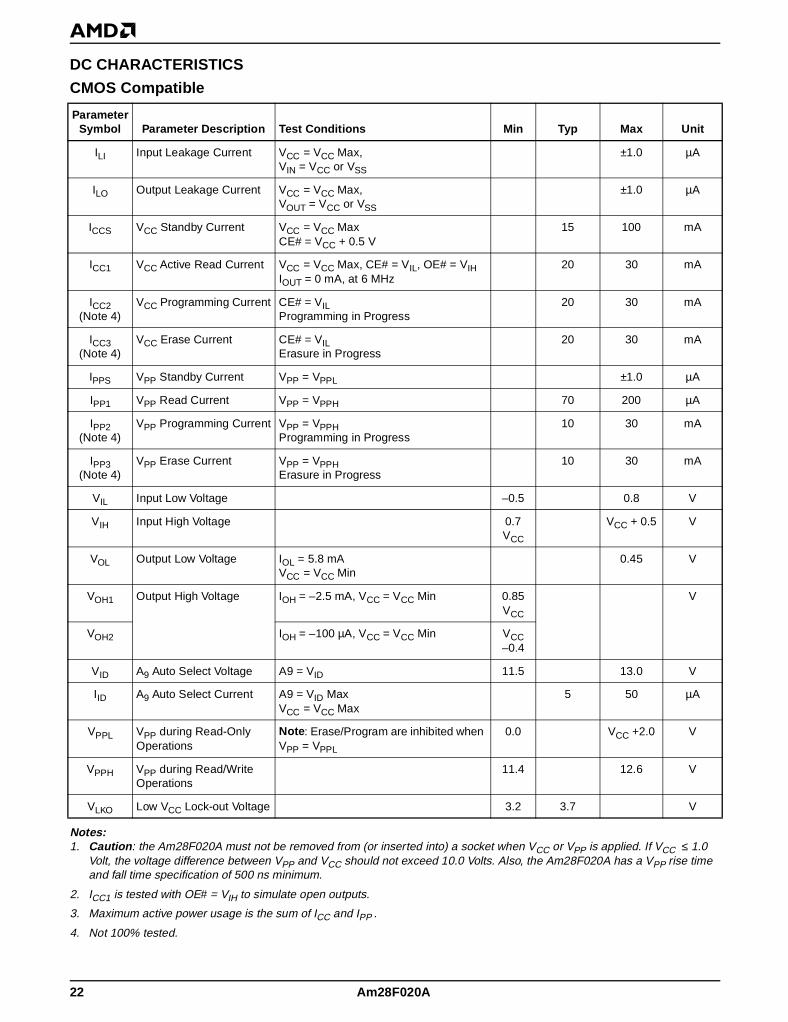
DC CHARACTERISTICS
CMOS Compatible
Notes:1. Caution : the Am28F020A must not be removed from (or inserted into) a socket when VCC or VPP is applied. If VCC ≤ 1.0
Volt, the voltage difference between VPP and VCC should not exceed 10.0 Volts. Also, the Am28F020A has a VPP rise time and fall time specification of 500 ns minimum.
2. ICC1 is tested with OE# = VIH to simulate open outputs.
3. Maximum active power usage is the sum of ICC and IPP .
4. Not 100% tested.
Parameter Symbol Parameter Description Test Conditions Min Typ Max Unit
ILI Input Leakage Current VCC = VCC Max, VIN = VCC or VSS
±1.0 µA
ILO Output Leakage Current VCC = VCC Max,VOUT = VCC or VSS
±1.0 µA
ICCS VCC Standby Current VCC = VCC MaxCE# = VCC + 0.5 V
15 100 mA
ICC1 VCC Active Read Current VCC = VCC Max, CE# = VIL, OE# = VIHIOUT = 0 mA, at 6 MHz
20 30 mA
ICC2(Note 4)
VCC Programming Current CE# = VILProgramming in Progress
20 30 mA
ICC3(Note 4)
VCC Erase Current CE# = VILErasure in Progress
20 30 mA
IPPS VPP Standby Current VPP = VPPL ±1.0 µA
IPP1 VPP Read Current VPP = VPPH 70 200 µA
IPP2(Note 4)
VPP Programming Current VPP = VPPHProgramming in Progress
10 30 mA
IPP3(Note 4)
VPP Erase Current VPP = VPPHErasure in Progress
10 30 mA
VIL Input Low Voltage –0.5 0.8 V
VIH Input High Voltage 0.7 VCC
VCC + 0.5 V
VOL Output Low Voltage IOL = 5.8 mAVCC = VCC Min
0.45 V
VOH1 Output High Voltage IOH = –2.5 mA, VCC = VCC Min 0.85 VCC
V
VOH2 IOH = –100 µA, VCC = VCC Min VCC –0.4
VID A9 Auto Select Voltage A9 = VID 11.5 13.0 V
IID A9 Auto Select Current A9 = VID MaxVCC = VCC Max
5 50 µA
VPPL VPP during Read-Only Operations
Note: Erase/Program are inhibited when VPP = VPPL
0.0 VCC +2.0 V
VPPH VPP during Read/Write Operations
11.4 12.6 V
VLKO Low VCC Lock-out Voltage 3.2 3.7 V
22 Am28F020A

Figure 7. Am28F020A - Average I CC Active vs. FrequencyVCC = 5.5 V, Addressing Pattern = Minmax
Data Pattern = Checkerboard
TEST CONDITIONS
17502D-16
Figure 8. Test Setup
Table 6. Test Specifications
30
25
20
15
10
5
0
0 1 2 3 4 5 6 7 8 9 10 11 12
17502D-15
-5502570125
°°
°°
°
CCCCC
ICC Active in mA
Frequency in MHz
2.7 kΩ
CL 6.2 kΩ
5.0 V
DeviceUnderTest
Note: Diodes are IN3064 or equivalent
Test Condition -70 All others Unit
Output Load 1 TTL gate
Output Load Capacitance, CL (including jig capacitance)
30 100 pF
Input Rise and Fall Times ≤10 ns
Input Pulse Levels 0.0–3.0 0.45–2.4 V
Input timing measurement reference levels
1.5 0.8, 2.0 V
Output timing measurement reference levels
1.5 0.8, 2.0 V
Am28F020A 23
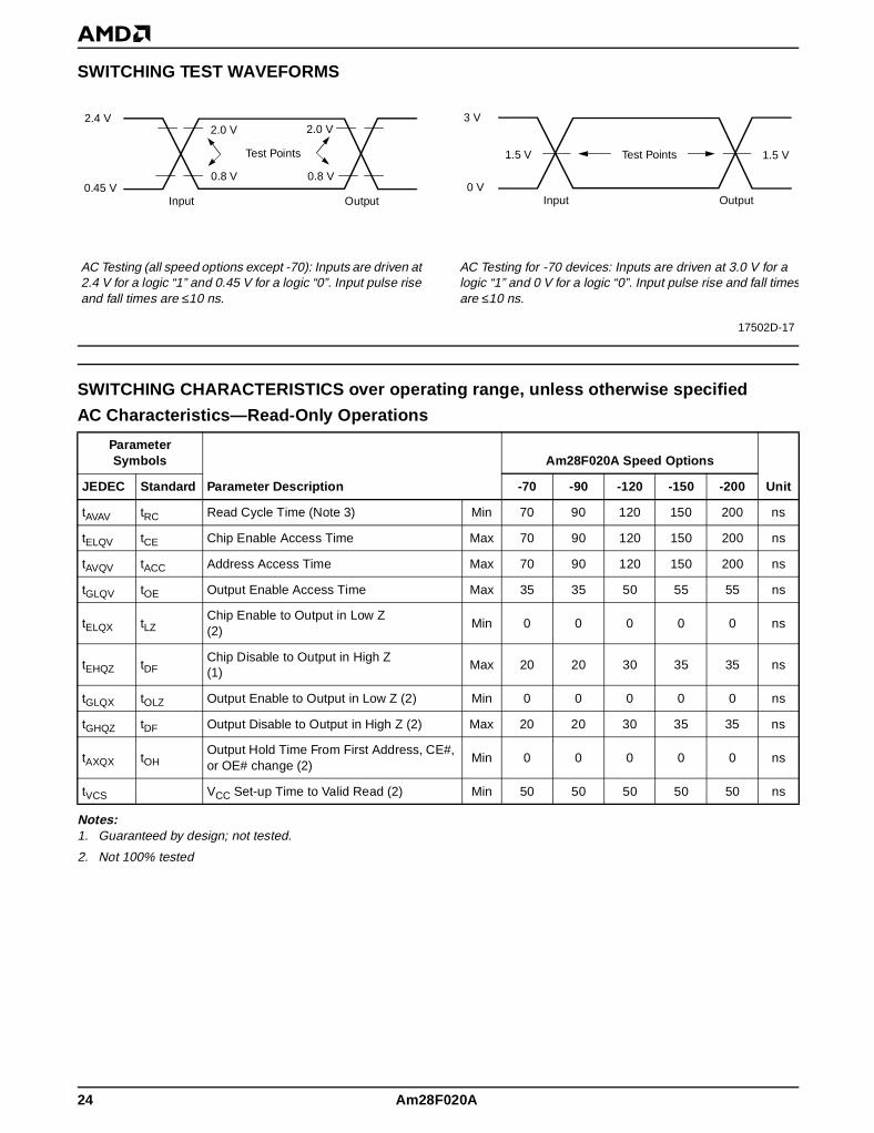
SWITCHING TEST WAVEFORMS
SWITCHING CHARACTERISTICS over operating range, unless otherwise specified
AC Characteristics—Read-Only Operations
Notes:1. Guaranteed by design; not tested.
2. Not 100% tested
Parameter Symbols Am28F020A Speed Options
JEDEC Standard Parameter Description -70 -90 -120 -150 -200 Unit
tAVAV tRC Read Cycle Time (Note 3) Min 70 90 120 150 200 ns
tELQV tCE Chip Enable Access Time Max 70 90 120 150 200 ns
tAVQV tACC Address Access Time Max 70 90 120 150 200 ns
tGLQV tOE Output Enable Access Time Max 35 35 50 55 55 ns
tELQX tLZChip Enable to Output in Low Z (2)
Min 0 0 0 0 0 ns
tEHQZ tDFChip Disable to Output in High Z (1)
Max 20 20 30 35 35 ns
tGLQX tOLZ Output Enable to Output in Low Z (2) Min 0 0 0 0 0 ns
tGHQZ tDF Output Disable to Output in High Z (2) Max 20 20 30 35 35 ns
tAXQX tOHOutput Hold Time From First Address, CE#, or OE# change (2)
Min 0 0 0 0 0 ns
tVCS VCC Set-up Time to Valid Read (2) Min 50 50 50 50 50 ns
17502D-17
3 V
0 VInput Output
1.5 V 1.5 VTest Points
AC Testing for -70 devices: Inputs are driven at 3.0 V for a logic “1” and 0 V for a logic “0”. Input pulse rise and fall timesare ≤10 ns.
2.4 V
0.45 VInput Output
Test Points
2.0 V 2.0 V
0.8 V0.8 V
AC Testing (all speed options except -70): Inputs are driven at 2.4 V for a logic “1” and 0.45 V for a logic “0”. Input pulse rise and fall times are ≤10 ns.
24 Am28F020A

AC Characteristics—Write (Erase/Program) Operations
Notes:1. Read timing characteristics during read/write operations are the same as during read-only operations. Refer to AC
Characteristics for Read Only operations.
2. Embedded Program Operation of 14 µs consists of 10 µs program pulse and 4 µs write recovery before read. This is the minimum time for one pass through the programming algorithm.
3. Embedded Erase operation of 5 sec consists of 4 sec array pre-programming time and one sec array erase time. This is a typical time for one embedded erase operation.
4. Not 100% tested.
Parameter Symbols Am28F020A Speed Options
JEDEC Standard Description -70 -90 -120 -150 -200 Unit
tAVAV tWC Write Cycle Time (4) Min 70 90 120 150 200 ns
tAVWL tAS Address Setup Time Min 0 0 0 0 0 ns
tWLAX tAH Address Hold Time Min 45 45 50 60 75 ns
tDVWH tDS Data Setup Time Min 45 45 50 50 50 ns
tWHDX tDH Data Hold Time Min 10 10 10 10 10 ns
tOEHOutput Enable Hold Time for Embedded Algorithm only
Min 10 10 10 10 10 ns
tGHWL Read Recovery Time Before Write Min 0 0 0 0 0 ns
tELWLE tCSE CE# Embedded Algorithm Setup Time Min 20 20 20 20 20 ns
tWHEH tCH CE# Hold Time Min 0 0 0 0 0 ns
tWLWH tWP Write Pulse Width Min 45 45 50 60 60 ns
tWHWL tWPH Write Pulse Width High Min 20 20 20 20 20 ns
tWHWH3 Embedded Program Operation (2) Min 14 14 14 14 14 µs
tWHWH4 Embedded Erase Operation (3) Typ 5 5 5 5 5 sec
tVPEL VPP Setup Time to Chip Enable Low (4) Min 100 100 100 100 100 ns
tVCS VCC Setup Time (4) Min 50 50 50 50 50 µs
tVPPR VPP Rise Time (4) 90% VPPH Min 500 500 500 500 500 ns
tVPPF VPP Fall Time (4) 90% VPPL Min 500 500 500 500 500 ns
tLKO VCC < VLKO to Reset (4) Min 100 100 100 100 100 ns
Am28F020A 25

KEY TO SWITCHING WAVEFORMS
SWITCHING WAVEFORMS
Figure 9. AC Waveforms for Read Operations
WAVEFORM INPUTS OUTPUTS
Steady
Changing from H to L
Changing from L to H
Don’t Care, Any Change Permitted Changing, State Unknown
Does Not Apply Center Line is High Impedance State (High Z)
Addresses
CE# (E#)
OE# (G#)
WE# (W#)
Data (DQ)
5.0 VVCC
Power-up, StandbyDevice and
Address SelectionOutputsEnabled
DataValid Standby, Power-down
Addresses Stable
High Z High Z
tWHGL
tAVQV (tACC)
tEHQZ (tDF)
tGHQZ (tDF)
tELQX (tLZ)tGLQX (tOLZ)
tELQV (tCE)
tGLQV (tOE)
tAXQX (tOH)
Output Valid
tAVAV (tRC)
tVCStVCS
17502D-18
0 V
26 Am28F020A
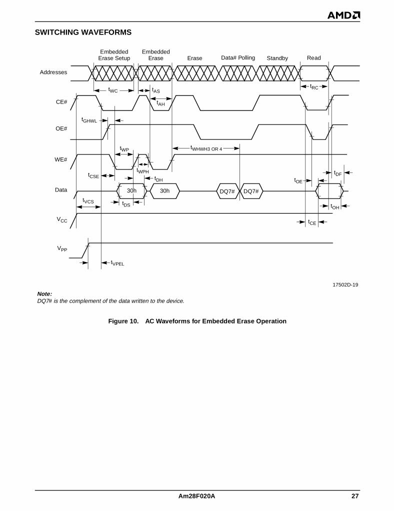
SWITCHING WAVEFORMS
tWC
DQ7#30h
tRC
Data# Polling Read
tDF
tOH
tCE
tOE
tDS
tCSEtWPH
tDH
tWP
tGHWL
tWHWH3 OR 4
Addresses
CE#
OE#
WE#
Data
VCC
VPP
EmbeddedErase Setup
EmbeddedErase Erase Standby
30h
tAH
tAS
tVCS
tVPEL
DQ7#
17502D-19
Note:DQ7# is the complement of the data written to the device.
Figure 10. AC Waveforms for Embedded Erase Operation
Am28F020A 27

SWITCHING WAVEFORMS
tWC
tDS
DQ7#DIN
tAS
tAH
tRC
Data# Polling Read
tDF
tOH
tCE
tOE
tWPHtDH
tWP
tGHWL
EmbeddedProgram Setup
EmbeddedProgram
tCSE
tWHWH3 OR 4
50h
PA
tVCS
tVPEL
PA
DQ7# DOUT
17502D-20
Notes:1. DIN is data input to the device.
2. DQ7# is the complement of the data written to the device.
3. DOUT is the data written to the device.
Figure 11. AC Waveforms for Embedded Pro grammin g Operation
Addresses
CE#
OE#
WE#
Data
VCC
VPP
28 Am28F020A
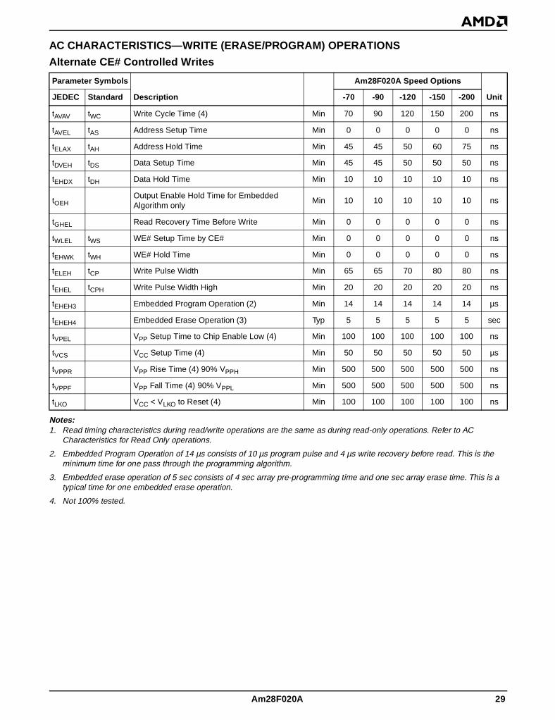
AC CHARACTERISTICS—WRITE (ERASE/PROGRAM) OPERATIONS
Alternate CE# Controlled Writes
Notes:1. Read timing characteristics during read/write operations are the same as during read-only operations. Refer to AC
Characteristics for Read Only operations.
2. Embedded Program Operation of 14 µs consists of 10 µs program pulse and 4 µs write recovery before read. This is the minimum time for one pass through the programming algorithm.
3. Embedded erase operation of 5 sec consists of 4 sec array pre-programming time and one sec array erase time. This is a typical time for one embedded erase operation.
4. Not 100% tested.
Parameter Symbols Am28F020A Speed Options
JEDEC Standard Description -70 -90 -120 -150 -200 Unit
tAVAV tWC Write Cycle Time (4) Min 70 90 120 150 200 ns
tAVEL tAS Address Setup Time Min 0 0 0 0 0 ns
tELAX tAH Address Hold Time Min 45 45 50 60 75 ns
tDVEH tDS Data Setup Time Min 45 45 50 50 50 ns
tEHDX tDH Data Hold Time Min 10 10 10 10 10 ns
tOEHOutput Enable Hold Time for Embedded Algorithm only
Min 10 10 10 10 10 ns
tGHEL Read Recovery Time Before Write Min 0 0 0 0 0 ns
tWLEL tWS WE# Setup Time by CE# Min 0 0 0 0 0 ns
tEHWK tWH WE# Hold Time Min 0 0 0 0 0 ns
tELEH tCP Write Pulse Width Min 65 65 70 80 80 ns
tEHEL tCPH Write Pulse Width High Min 20 20 20 20 20 ns
tEHEH3 Embedded Program Operation (2) Min 14 14 14 14 14 µs
tEHEH4 Embedded Erase Operation (3) Typ 5 5 5 5 5 sec
tVPEL VPP Setup Time to Chip Enable Low (4) Min 100 100 100 100 100 ns
tVCS VCC Setup Time (4) Min 50 50 50 50 50 µs
tVPPR VPP Rise Time (4) 90% VPPH Min 500 500 500 500 500 ns
tVPPF VPP Fall Time (4) 90% VPPL Min 500 500 500 500 500 ns
tLKO VCC < VLKO to Reset (4) Min 100 100 100 100 100 ns
Am28F020A 29
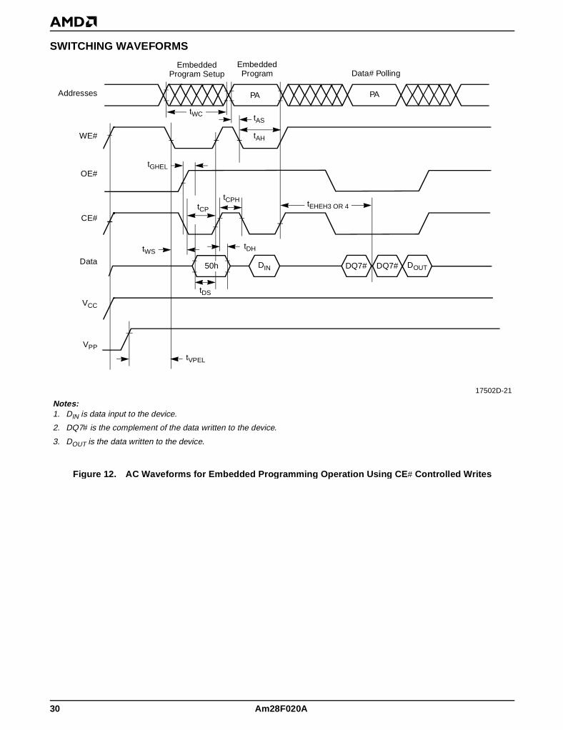
SWITCHING WAVEFORMS
tVPEL
tWC
Data# Polling
PA
DQ7#DIN
tAS
tAH
tGHEL
tDH
tCPH tEHEH3 OR 4
tWS
tDS
tCP
EmbeddedProgram Setup
EmbeddedProgram
PA
DOUTDQ7#
17502D-21
Notes:1. DIN is data input to the device.
2. DQ7# is the complement of the data written to the device.
3. DOUT is the data written to the device.
Figure 12. AC Waveforms for Embedded Pro grammin g Operation Usin g CE# Controlled Writes
Addresses
WE#
OE#
CE#
Data
VCC
VPP
50h
30 Am28F020A

ERASE AND PROGRAMMING PERFORMANCE
Notes:1. 25°C, 12 V VPP .
2. Maximum time specified is lower than worst case. Worst case is derived from the Embedded Algorithm internal counter which allows for a maximum 6000 pulses for both program and erase operations. Typical worst case for program and erase is significantly less than the actual device limit.
3. Typical worst case = 84 µs. DQ5 = “1” only after a byte takes longer than 96 ms to program.
LATCHUP CHARACTERISTICS
PIN CAPACITANCE
Note: Sampled, not 100% tested. Test conditions TA = 25°C, f = 1.0 MHz.
DATA RETENTION
Parameter
Limits
CommentsMinTyp
(Note 1)Max
(Note 2) Unit
Chip Erase Time 1 10 sec Excludes 00h programming prior to erasure
Chip Programming Time 4 25 sec Excludes system-level overhead
Write/Erase Cycles 100,000 Cycles
Byte Programming Time 14 µs
96(Note 3)
ms
Parameter Min Max
Input Voltage with respect to VSS on all pins except I/O pins (Including A9 and VPP) –1.0 V 13.5 V
Input Voltage with respect to VSS on all pins I/O pins –1.0 V VCC + 1.0 V
Current –100 mA +100 mA
Includes all pins except VCC. Test conditions: VCC = 5.0 V, one pin at a time.
Parameter Symbol Parameter Description Test Conditions Typ Max Unit
CIN Input Capacitance VIN = 0 8 10 pF
COUT Output Capacitance VOUT = 0 8 12 pF
CIN2 VPP Input Capacitance VPP = 0 8 12 pF
Parameter Test Conditions Min Unit
Minimum Pattern Data Retention Time150°C 10 Years
125°C 20 Years
Am28F020A 31

PHYSICAL DIMENSIONS
PD032—32-Pin Plastic DIP (measured in inches)
PL032—32-Pin Plastic Leaded Chip Carrier (measured in inches)
Pin 1 I.D.
1.6401.670
.530
.580
.005 MIN.045.065
.090
.110
.140
.225
.120
.160.016.022
SEATING PLANE
.015
.060
16-038-S_AGPD 032EC755-28-97 lv
32 17
16.630.700
0°10°
.600
.625
.009
.015
.050 REF..026.032
TOP VIEW
Pin 1 I.D.
.485
.495.447.453
.585
.595
.547
.553
16-038FPO-5PL 032DA796-28-94 aeSIDE VIEW
SEATINGPLANE
.125
.140
.009
.015
.080
.095
.042
.056
.013
.021
.400REF.
.490
.530
32 Am28F020A

PHYSICAL DIMENSIONS
TS032—32-Pin Standard Thin Small Outline Package (measured in millimeters)
Pin 1 I.D.
1
18.3018.50
7.908.10
0.50 BSC
0.050.15
0.951.05
16-038-TSOP-2TS 032DA953-25-97 lv
19.8020.20
1.20MAX
0.500.70
0.100.210°
5°
0.080.20
Am28F020A 33
PHYSICAL DIMENSIONS
TSR032—32-Pin Reversed Thin Small Outline Package (measured in millimeters)
1
18.3018.50
19.8020.20
7.908.10
0.50 BSC
0.050.15
0.951.05
16-038-TSOP-2TSR032DA953-25-97 lv
Pin 1 I.D.
1.20MAX
0.500.70
0.100.210°
5°
0.080.20
34 Am28F020A
DATA SHEET REVISION SUMMARY FOR AM28F020A
Revision C+1Distinctive Characteristics:
High Performance: The fastest speed option availableis now 70 ns.
General Description:
Paragraph 2: Changed fastest speed option to 70 ns.
Product Selector Guide:
Added -70, deleted -95 and -250 speed options.
Ordering Information, Standard Products:
The -70 speed option is now listed in the example.
Valid Combinations: Added -70, deleted -95 and -250combinations.
Erase, Program, and Read Mode:
Corrected the subheading to read “VPP = 12.0 V ± 5%”.
Operating Ranges:
VCC Supply Voltages: Added -70, deleted -95 and -250speed options.
AC Characteristics:
Read Only Operations Characteristics: Added the -70column and test conditions.
Deleted -95 and -250 speed options.
AC Characteristics:
Write/Erase/Program Operations, Alternate CE# Con-trolled Writes: Added the -70 column. Deleted -95 and-250 speed options.
Switching Test Waveforms:
In the 3.0 V waveform caption, changed -95 to -70.
Revision DMatched formatting to other current data sheets.
Revision D+1Programming In A PROM Programmer:
Deleted the paragraph “(Refer to the AUTO SELECTparagraph in the ERASE, PROGRAM, and READMODE section for programming the Flash memory de-vice in-system).”
Trademarks
Copyright © 1998 Advanced Micro Devices, Inc. All rights reserved.
ExpressFlash is a trademark of Advanced Micro Devices, Inc.
AMD, the AMD logo, and combinations thereof are registered trademarks of Advanced Micro Devices, Inc.
Product names used in this publication are for identification purposes only and may be trademarks of their respective companies.
Am28F020A 35
Related Documents