Microchip Proprietary Information ©2013 Silicon Storage Technology, Inc. DS75054A 01/13 Data Sheet www.microchip.com Features • High Gain: – Typically 33 dB gain across 2.4–2.5 GHz over tempera- ture -40°C to +85°C • High linear output power: – >30 dBm P1dB - Please refer to “Absolute Maximum Stress Ratings” on page 5 – Meets 802.11g OFDM spectrum mask requirement up to 28.5 dBm – EVM~3% up to 25 dBm for 54 Mbps 802.11g signal – 2.5% EVM up to 23.5 dBm, 802.11n, HT40 – 1.75% EVM up to 21.5 dBm, 802.11ac MCS8 – Meets 802.11b ACPR requirement up to 28.5 dBm • High-speed power-up/down – Turn on/off time (10%-90%) <100 ns • 10:1 VSWR survivability (unconditionally stable up to 28.5 dBm) • On-chip power detection – 20 dB dynamic range – VSWR- and temperature-insensitive • Simple input/output matching • Packages available – 16-contact VQFN (3mm x 3mm) • All non-Pb (lead-free) devices are RoHS compliant Applications • WLAN (IEEE 802.11b/g/n) • AP router • WiMax (IEEE 802.16e) • Home RF • Cordless phones • 2.4 GHz ISM wireless equipment • 1.8 GHz Pico Cell 2.4 GHz High-Power and High-Gain Power Amplifier SST12CP11 SST12CP11 is a high-power and high-gain power amplifier (PA) based on the highly-reliable InGaP/GaAs HBT technology.This PA can be easily configured for high-power applications with good power-added efficiency while operating over the 2.4-2.5 GHz frequency band. It can also be configured to operate at 1.8 GHz for Pico Cell applications. SST12CP11 typically provides 33 dB gain and has excellent linearity, typically ~3% EVM at 25 dBm output power at 54 Mbps 802.11g operation while meeting 802.11g spectrum mask at 28.5 dBm. The power amplifier IC includes an output power detector that has a wide dynamic range and is VSWR- insensitive. SST12CP11 features easy board-level usage along with high-speed power-up/-down control and is offered in 16-contact VQFN package.

Welcome message from author
This document is posted to help you gain knowledge. Please leave a comment to let me know what you think about it! Share it to your friends and learn new things together.
Transcript

Microchip Proprietary Information©2013 Silicon Storage Technology, Inc. DS75054A 01/13
Data Sheet
www.microchip.com
Features• High Gain:
– Typically 33 dB gain across 2.4–2.5 GHz over tempera-ture -40°C to +85°C
• High linear output power: – >30 dBm P1dB
- Please refer to “Absolute Maximum Stress Ratings” on page 5
– Meets 802.11g OFDM spectrum mask requirement up to 28.5 dBm
– EVM~3% up to 25 dBm for 54 Mbps 802.11g signal– 2.5% EVM up to 23.5 dBm, 802.11n, HT40– 1.75% EVM up to 21.5 dBm, 802.11ac MCS8– Meets 802.11b ACPR requirement up to 28.5 dBm
• High-speed power-up/down– Turn on/off time (10%-90%) <100 ns
• 10:1 VSWR survivability (unconditionally stable up to 28.5 dBm)
• On-chip power detection– 20 dB dynamic range– VSWR- and temperature-insensitive
• Simple input/output matching
• Packages available– 16-contact VQFN (3mm x 3mm)
• All non-Pb (lead-free) devices are RoHS compliant
Applications• WLAN (IEEE 802.11b/g/n)
• AP router
• WiMax (IEEE 802.16e)
• Home RF
• Cordless phones
• 2.4 GHz ISM wireless equipment
• 1.8 GHz Pico Cell
2.4 GHz High-Power and High-Gain Power AmplifierSST12CP11
SST12CP11 is a high-power and high-gain power amplifier (PA) based on thehighly-reliable InGaP/GaAs HBT technology.This PA can be easily configured forhigh-power applications with good power-added efficiency while operating over the2.4-2.5 GHz frequency band. It can also be configured to operate at 1.8 GHz forPico Cell applications. SST12CP11 typically provides 33 dB gain and has excellentlinearity, typically ~3% EVM at 25 dBm output power at 54 Mbps 802.11g operationwhile meeting 802.11g spectrum mask at 28.5 dBm. The power amplifier ICincludes an output power detector that has a wide dynamic range and is VSWR-insensitive. SST12CP11 features easy board-level usage along with high-speedpower-up/-down control and is offered in 16-contact VQFN package.
Microchip Proprietary Information©2013 Silicon Storage Technology, Inc. DS75054A 01/13
2
2.4 GHz High-Power and High-Gain Power AmplifierSST12CP11
Data Sheet
Product DescriptionSST12CP11 is a high-power and high-gain power amplifier (PA) based on the highly-reliable InGaP/GaAs HBT technology.
This PA can be easily configured for high-power applications with high power-added efficiency whileoperating over the 2.4-2.5 GHz frequency band. It typically provides 33 dB gain with 15% power-addedefficiency @ POUT = 25 dBm for 802.11g.
SST12CP11 has excellent linearity, typically 3% added EVM at 25 dBm output power with 54 Mbps802.11g operation while meeting 802.11g spectrum mask at 28.5 dBm. SST12CP11 also has a single-ended power detector which lowers the users’ cost for power control.
The power amplifier IC also features easy board-level usage along with high-speed power-up/-downcontrol.
SST12CP11 is offered in 16-contact VQFN package. See Figure 2 for pin assignments and Table 1 forpin descriptions.

Microchip Proprietary Information©2013 Silicon Storage Technology, Inc. DS75054A 01/13
3
2.4 GHz High-Power and High-Gain Power AmplifierSST12CP11
Data Sheet
Functional Blocks
Figure 1: Functional Block Diagram
2
5 6 8
16
VC
C1
15
1
14
VC
C2
NC
4 9
11
12
10
13
NC
VC
Cb
GN
D
VR
EF
2
DE
TVCC3
RFOUT
RFOUT
NC
NC
3
RFIN
RFIN
VREF1
Bias Circuit
7
1403 B1.1

Microchip Proprietary Information©2013 Silicon Storage Technology, Inc. DS75054A 01/13
4
2.4 GHz High-Power and High-Gain Power AmplifierSST12CP11
Data Sheet
Pin Assignments
Figure 2: Pin Assignments for 16-contact VQFN
Pin Descriptions
Table 1: Pin Description
Symbol Pin No. Pin Name Type1
1. I=Input, O=Output
Function
GND 0 Ground The center pad should be connected to RF ground with several low inductance, low resistance vias.
NC 1 No Connection Unconnected pins.
RFIN 2 I RF input, DC decoupled
RFIN 3 I RF input, DC decoupled
VREF1 4 Power Supply PWR 1st stage, idle-current control
VCCb 5 Power Supply PWR Supply voltage for bias circuit
GND 6 Ground
VREF2 7 Power supply PWR 2nd and 3rd stage, idle-current control
Det 8 O On-chip power detector
NC 9 No Connection Unconnected pins.
RFOUT 10 O RF output
RFOUT 11 O RF output
VCC3 12 Power Supply PWR Power supply, 3rd stage
NC 13 No Connection Unconnected pins.
VCC2 14 Power Supply PWR Power supply, 2nd stage
NC 15 No Connection Unconnected pins.
VCC1 16 Power Supply PWR Power supply, 1st stageT1.0 75054
5 6 8
16
VC
C1
15 14
VC
C2
NC
9
11
12
10
13
NC
VC
Cb
GN
D
VR
EF
2
DE
TVCC3
RFOUT
RFOUT
NC
2
1
4
3
NC
RFIN
RFIN
VREF1
7
1403 16-vqfn P1.0
Top View(contacts facing down)
RF and DC GND0

Microchip Proprietary Information©2013 Silicon Storage Technology, Inc. DS75054A 01/13
5
2.4 GHz High-Power and High-Gain Power AmplifierSST12CP11
Data Sheet
Electrical SpecificationsThe AC and DC specifications for the power amplifier interface signals. Refer to Table 3 for the DC volt-age and current specifications. Refer to Figures 3 through 21 for the RF performance.
Absolute Maximum Stress Ratings (Applied conditions greater than those listed under “AbsoluteMaximum Stress Ratings” may cause permanent damage to the device. This is a stress rating only andfunctional operation of the device at these conditions or conditions greater than those defined in theoperational sections of this data sheet is not implied. Exposure to absolute maximum stress rating con-ditions may affect device reliability.)
Input power to pins 2 and 3 (PIN) . . . . . . . . . . . . . . . . . . . . . . . . . . . . . . . . . . . . . . . . . . . . . . . . -3 dBmSupply Voltage at pins 5, 12, 14, 16 (VCC). . . . . . . . . . . . . . . . . . . . . . . . . . . . . . . . . . . . . . . . . . +5.5VReference voltage to pins 4 (VREF1) and pin 7 (VREF2) . . . . . . . . . . . . . . . . . . . . . . . . . . . . . . . . +3.1VDC supply current (ICC) . . . . . . . . . . . . . . . . . . . . . . . . . . . . . . . . . . . . . . . . . . . . . . . . . . . . . . 650 mAOperating Temperature (TA). . . . . . . . . . . . . . . . . . . . . . . . . . . . . . . . . . . . . . . . . . . . . -40ºC to +85ºCStorage Temperature (TSTG) . . . . . . . . . . . . . . . . . . . . . . . . . . . . . . . . . . . . . . . . . . . -40ºC to +120ºCMaximum Junction Temperature (TJ). . . . . . . . . . . . . . . . . . . . . . . . . . . . . . . . . . . . . . . . . . . . .+150ºCSurface Mount Solder Reflow Temperature . . . . . . . . . . . . . . . . . . . . . . . . . . . . 260°C for 10 seconds
Table 2: Operating Range
Range Ambient Temp VCC
Industrial -40°C to +85°C 5.0VT2.1 75054
Table 3: DC Electrical Characteristics at 25ºC
Symbol Parameter Min. Typ Max. Unit
VCC Supply Voltage at pins 5, 12, 14, 16 4.0 5.0 5.25 V
ICC Average Current
for 802.11g, 28.5 dBm 570 mA
for 802.11b, 28.5 dBm 575 mA
ICQ Idle current for 802.11g to meet EVM<3% @24.5 dBm 230 mA
VREG 1st reference voltage with 56Ω resistor and 2nd / 3rd reference voltage with 6.2Ω resistor
2.85 2.9 3.0 V
T3.1 75054

Microchip Proprietary Information©2013 Silicon Storage Technology, Inc. DS75054A 01/13
6
2.4 GHz High-Power and High-Gain Power AmplifierSST12CP11
Data Sheet
Table 4: AC Electrical Characteristics for Configuration at 25ºC
Symbol Parameter Min. Typ Max. Unit
FL-U Frequency range in 802.11b/g applications (see Figure 22)
2400 2500 MHz
POUT
Output power at 3% EVM with 802.11g OFDM at 54 Mbps
25 dBm
Output power at 2.5% EVM with 802.11n HT40 23.5 dBm
Output power at 1.75% EVM with 802.11ac MCS8 21.5 dBm
Output power meeting 802.11g spectral mask 28 dBm
Output power meeting 802.11n HT40 spectral mask 24.5 dBm
Output power meeting 802.11ac spectral mask 24 dBm
Output power meeting 802.11b spectral mask 28.5 dBm
G
Power gain for 802.11b/g 32 34 dB
Power gain for 802.11n 33 dB
Power Gain for 802.11ac 30 dB
GVAR Gain variation over each band (2500 MHz) ±0.5 dB
2f Harmonics at 28 dBm, 802.11b mask compliance -21 dBm/MHz
2f Harmonics at 24.5 dBm -38 dBm/MHzT4.2 75054
Microchip Proprietary Information©2013 Silicon Storage Technology, Inc. DS75054A 01/13
7
2.4 GHz High-Power and High-Gain Power AmplifierSST12CP11
Data Sheet
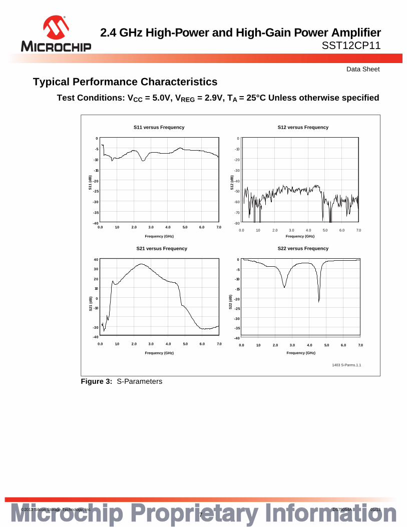
Typical Performance CharacteristicsTest Conditions: VCC = 5.0V, VREG = 2.9V, TA = 25°C Unless otherwise specified
Figure 3: S-Parameters
1403 S-Parms.1.1
Frequency (GHz)
S11
(d
B)
S12 versus Frequency
S12
(d
B)
S11 versus Frequency
S21 versus Frequency
Frequency (GHz)
S21
(d
B)
S22 versus Frequency
Frequency (GHz)
S22
(d
B)
-40
-35
-30
-25
-20
-15
-10
-5
0
0.0 1.0 2.0 3.0 4.0 5.0 6.0 7.0-80
-70
-60
-50
-40
-30
-20
-10
0
0.0 1.0 2.0 3.0 4.0 5.0 6.0 7.0
Frequency (GHz)
-40
-30
-10
0
10
20
30
40
0.0 1.0 2.0 3.0 4.0 5.0 6.0 7.0
-40
-35
-30
-25
-20
-15
-10
-5
0
0.0 1.0 2.0 3.0 4.0 5.0 6.0 7.0

Microchip Proprietary Information©2013 Silicon Storage Technology, Inc. DS75054A 01/13
8
2.4 GHz High-Power and High-Gain Power AmplifierSST12CP11
Data Sheet
802.11ac ApplicationsTypical Performance CharacteristicsTest Conditions: VCC = 5.0V, VREG = 3.20V, TA = 25°C, MCS8 signal, unless otherwise specified
Figure 4: EVM versus Output Power
Figure 5: Power Gain versus Output Power
75054 F21.0
0
1
2
3
4
5
6
7
8
9
10
0 1 2 3 4 5 6 7 8 9 10 11 12 13 14 15 16 17 18 19 20 21 22 23 24 25
EVM
(%)
Output Power (dBm)
EVM versus Output Power
Freq=2.412GHzFreq=2.442GHzFreq=2.472 GHz
75054 F22.0
20
22
24
26
28
30
32
34
5 6 7 8 9 10 11 12 13 14 15 16 17 18 19 20 21 22 23 24 25
Pow
er G
ain
(dB)
Output Power (dBm)
Power Gain versus Output Power
Freq=2.412GHz
Freq=2.442GHz
Freq=2.472 GHz

Microchip Proprietary Information©2013 Silicon Storage Technology, Inc. DS75054A 01/13
9
2.4 GHz High-Power and High-Gain Power AmplifierSST12CP11
Data Sheet
802.11ac Applications (continued)
Figure 6: Supply Current versus Output Power
Figure 7: Detector Characteristic versus Output Power
75054 F23.0
400
420
440
460
480
500
520
540
560
580
600
0 1 2 3 4 5 6 7 8 9 10 11 12 13 14 15 16 17 18 19 20 21 22 23 24 25
Supp
ly C
urre
nt (m
A)
Output Power (dBm)
Supply Current versus Output Power
Freq=2.412GHzFreq=2.442GHzFreq=2.472 GHz
75054 F24.0
0.000.100.200.300.400.500.600.700.800.901.001.101.201.301.401.50
0 1 2 3 4 5 6 7 8 9 10 11 12 13 14 15 16 17 18 19 20 21 22 23 24 25 26
Dete
ctor
Vol
tage
(V)
Output Power (dBm)
Detector Voltage versus Output Power
Freq=2.412GHz
Freq=2.442GHz
Freq=2.472 GHz

Microchip Proprietary Information©2013 Silicon Storage Technology, Inc. DS75054A 01/13
10
2.4 GHz High-Power and High-Gain Power AmplifierSST12CP11
Data Sheet
802.11ac Applications (continued)
Figure 8: Typical Schematic for 802.11ac Applications
2
5 6 7 8
9
11
16 15
1
50Ω
1.8 pF
50Ω /110 mil
50Ω
GND
VREG
14 13
0.1 µF
Vcc
4
12
10
0.1 µF
6.8 Ω
3
DNI
VDET75054 Schematic.3.0
Suggested operation conditions:
1. VCC = 5.0V/ VREG = 3.2V2. Center slug to RF ground
0.1 µF
VCC
12 nH (0805 size)
1000 pF
4.7 nH
50Ω /30mil
1.2 pF
8.2 pF
0.1 µF
0.1 µF56 Ω
Bias Circuit
4.7 µF
0.1 µF
50Ω /90 mil50Ω /90 mil

Microchip Proprietary Information©2013 Silicon Storage Technology, Inc. DS75054A 01/13
11
2.4 GHz High-Power and High-Gain Power AmplifierSST12CP11
Data Sheet
802.11n ApplicationsTypical Performance CharacteristicsTest Conditions: VCC = 5.0V, VREG = 2.95V, TA = 25°C, HT40 signal, unless otherwise specified
Figure 9: EVM versus Output Power
Figure 10:Power Gain versus Output Power
1403 F17.0
0
1
2
3
4
5
6
7
8
9
10
0 1 2 3 4 5 6 7 8 9 10 11 12 13 14 15 16 17 18 19 20 21 22 23 24 25 26
EVM
(%)
Output Power (dBm)
EVM versus Output Power
Freq=2.412GHzFreq=2.442GHzFreq=2.472 GHz
1403 F18.0
20
22
24
26
28
30
32
34
36
38
5 6 7 8 9 10 11 12 13 14 15 16 17 18 19 20 21 22 23 24 25
Pow
er G
ain
(dB)
Output Power (dBm)
Power Gain versus Output Power
Freq=2.412GHz
Freq=2.442GHz
Freq=2.472 GHz

Microchip Proprietary Information©2013 Silicon Storage Technology, Inc. DS75054A 01/13
12
2.4 GHz High-Power and High-Gain Power AmplifierSST12CP11
Data Sheet
802.11n Applications (continued)
Figure 11:Supply Current versus Output Power
Figure 12:Detector Characteristic versus Output Power
1403 F19.0
200220240260280300320340360380400420440460480500
0 1 2 3 4 5 6 7 8 9 10 11 12 13 14 15 16 17 18 19 20 21 22 23 24 25 26
Supp
ly C
urre
nt (m
A)
Output Power (dBm)
Supply Current versus Output Power
Freq=2.412GHzFreq=2.442GHzFreq=2.472 GHz
1403 F 20.0
0.000.100.200.300.400.500.600.700.800.901.001.101.201.301.401.50
0 1 2 3 4 5 6 7 8 9 10 11 12 13 14 15 16 17 18 19 20 21 22 23 24 25 26
Dete
ctor
Vol
tage
(V)
Output Power (dBm)
Detector Voltage versus Output Power
Freq=2.412GHz
Freq=2.442GHz
Freq=2.472 GHz

Microchip Proprietary Information©2013 Silicon Storage Technology, Inc. DS75054A 01/13
13
2.4 GHz High-Power and High-Gain Power AmplifierSST12CP11
Data Sheet
802.11n Applications (continued)
Figure 13:Typical Schematic for 802.11n Applications
2
5 6 7 8
9
11
16 15
1
50Ω
1.8 pF
50Ω /110 mil
50Ω
GND
VREG
14 13
0.1 µF
Vcc
4
12
10
0.1 µF
6.8 Ω
3
DNI
VDET75054 Schematic.2.0
Suggested operation conditions:
1. VCC = 5.0V/ VREG = 2.95V2. Center slug to RF ground
0.1 µF
VCC
12 nH (0805 size)
1000 pF
4.7 nH
50Ω /50mil
1.0 pF
8.2 pF
0.1 µF
0.1 µF56 Ω
Bias Circuit
4.7 µF
0.1 µF
50Ω /90 mil50Ω /90 mil

Microchip Proprietary Information©2013 Silicon Storage Technology, Inc. DS75054A 01/13
14
2.4 GHz High-Power and High-Gain Power AmplifierSST12CP11
Data Sheet
802.11b/g ApplicationsTypical Performance CharacteristicsTest Conditions: VCC = 5.0V, VREG = 2.9V, TA = 25°C, unless otherwise specified 54 Mbps 802.11g OFDM Signal
Figure 14:EVM versus Output Power
Figure 15:EVM versus Output Power over Temperature, VCC= 5, VREG = 2.9
1403 F4.2
0
1
2
3
4
5
6
7
8
9
10
0 1 2 3 4 5 6 7 8 9 10 1112131415161718192021222324252627282930
EVM
(%)
Output Power (dBm)
EVM versus Output Power
EVM versus Output Power overTemperature
Temperature
EV
M (
%)
1403 F5.1
0
1
2
3
4
5
6
7
8
9
10
13 14 15 16 17 18 19 20 21 22 23 24 25 26 27 28
0'C25'C85'C

Microchip Proprietary Information©2013 Silicon Storage Technology, Inc. DS75054A 01/13
15
2.4 GHz High-Power and High-Gain Power AmplifierSST12CP11
Data Sheet
802.11b/g Applications (continued)Test Conditions: VCC = 5.0V, VREG = 2.9V, TA = 25°C, 54 Mbps 802.11g OFDM Signal
Figure 16:Power Gain versus Output Power, measured with sequence only, see Figure 22
Figure 17:Total Current Consumption versus Output Power, see Figure 22
1403 F14.3
202122232425262728293031323334353637
5 6 7 8 9 10 11 12 13 14 15 16 17 18 19 20 21 22 23 24 25 26 27 28 29 30
Pow
er G
ain
(dB
)
Output Power (dBm)
Power Gain versus Output Power
2412
2442
2472
1403 F6.2
100120140160180200220240260280300320340360380400420440460480500520540560580600
0 1 2 3 4 5 6 7 8 9 10 1112131415161718192021222324252627282930
Supp
ly C
urre
nt (m
A)
Output Power (dBm)
Supply Current versus Output Power
2412
2442
2472
Microchip Proprietary Information©2013 Silicon Storage Technology, Inc. DS75054A 01/13
16
2.4 GHz High-Power and High-Gain Power AmplifierSST12CP11
Data Sheet
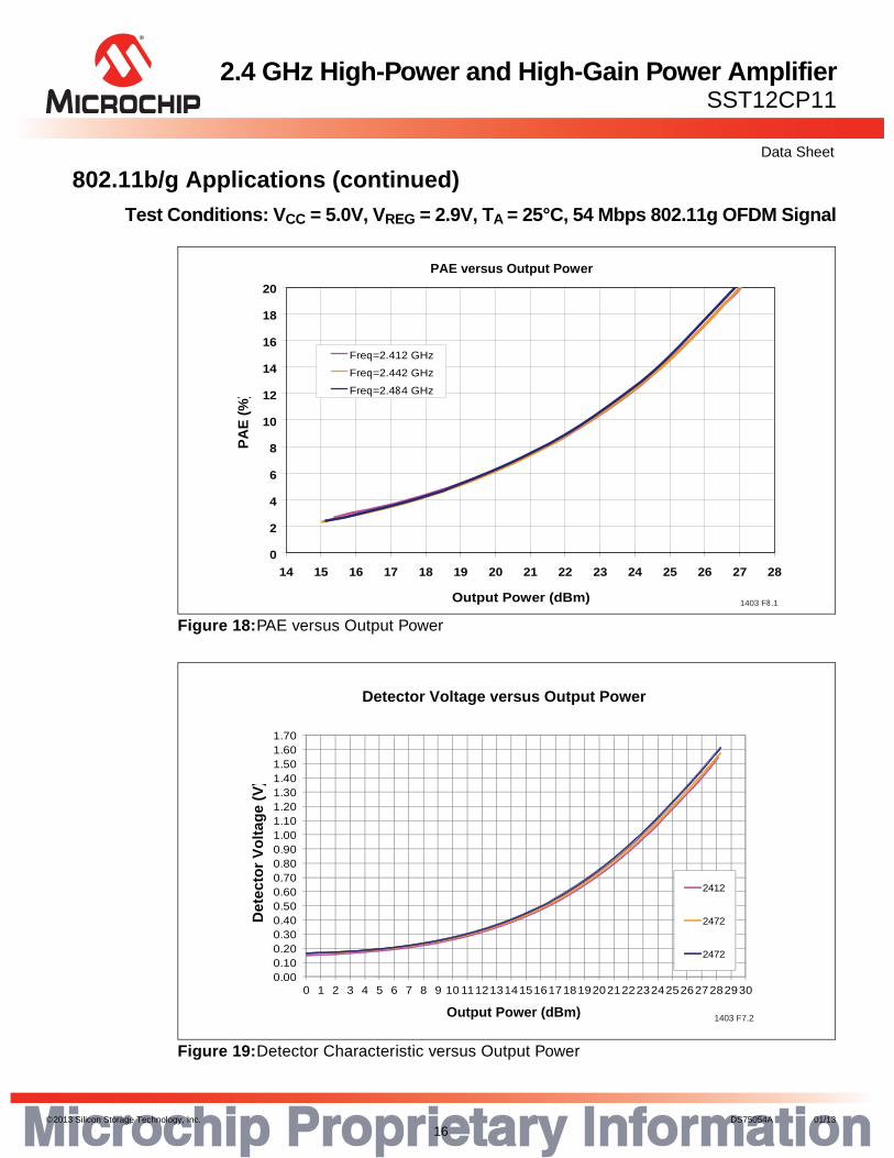
802.11b/g Applications (continued)Test Conditions: VCC = 5.0V, VREG = 2.9V, TA = 25°C, 54 Mbps 802.11g OFDM Signal
Figure 18:PAE versus Output Power
Figure 19:Detector Characteristic versus Output Power
1403 F8.1
PAE versus Output Power
Output Power (dBm)
PA
E (
%)
0
2
4
6
8
10
12
14
16
18
20
14 15 16 17 18 19 20 21 22 23 24 25 26 27 28
Freq=2.412 GHz
Freq=2.442 GHz
Freq=2.484 GHz
1403 F7.2
0.000.100.200.300.400.500.600.700.800.901.001.101.201.301.401.501.601.70
0 1 2 3 4 5 6 7 8 9 10 1112131415161718192021222324252627282930
Det
ecto
r Vol
tage
(V)
Output Power (dBm)
Detector Voltage versus Output Power
2412
2472
2472

Microchip Proprietary Information©2013 Silicon Storage Technology, Inc. DS75054A 01/13
17
2.4 GHz High-Power and High-Gain Power AmplifierSST12CP11
Data Sheet
802.11b/g Applications (continued)Test Conditions: VCC = 5.0V, VREG = 2.9V, TA = 25°C, 54 Mbps 802.11g OFDM Signal
Figure 20:802.11g Spectrum Mask at 28 dBm
Test Conditions: VCC = 5.0V, VREG = 2.9V, TA=25°C, 1 Mbps 802.11b CCK signal
Figure 21:802.11b Spectrum Mask at 28 dBm
-80
-70
-60
-50
-40
-30
-20
-10
0
2.392 2.492
Frequency(GHz)
Am
pli
tud
e(d
B)
2.442
1403 F9.0
1403 F10.0
-90
-80
-70
-60
-50
-40
-30
-20
-10
0
2.392 2.492
Frequency(GHz)
Am
plit
ud
e(d
B)
2.442

Microchip Proprietary Information©2013 Silicon Storage Technology, Inc. DS75054A 01/13
18
2.4 GHz High-Power and High-Gain Power AmplifierSST12CP11
Data Sheet
802.11b/g Applications (continued)
Figure 22:Typical Schematic for High-Power 802.11b/g Applications
2
5 6 7 8
9
11
16 15
1
50 SMA_END
1.8 pF
50 /90 mil50
SMA_END
GND
VREG
14 13
0.1 µF
Vcc
4
12
10
100 pF
6.2
3
DNI
VDET1403 Schematic.1.2
Suggested operation conditions:
1. VCC = 5.0V/ VREG = 2.9V2. R1=56 and R2=6.2 3. Center slug to RF ground
100pF
VCC
12 nH (0805 size)
1000 pF
4.7 nH
50 /108 mil
1.5 pF
8.2 pF
0.1 µF
0.1 µF56Ω
Bias Circuit
10 µF
0.1 µF
50 /90 mil50 /90 mil

Microchip Proprietary Information©2013 Silicon Storage Technology, Inc. DS75054A 01/13
19
2.4 GHz High-Power and High-Gain Power AmplifierSST12CP11
Data Sheet
1.8 GHz ApplicationsTypical Performance CharacteristicsTest Conditions: VCC = 5.0V, VREG = 2.95V, TA = 25°C, 54 Mbps 802.11g OFDM signal, unless otherwise specified
Figure 23:Typical Schematic for Pico Cell Applications
Table 5: AC Electrical Characteristics for Pico Cell Applications
Symbol Parameter Min. Typ Max. Unit
FL-U Frequency range 1800 2000 MHz
G Gain 31 dB
P Power at 3% EVM 24 dBm
PSAT Output Power at 1 dB compression 27 dBm
ICC Current at 24 dBm 400 mA
PAE Power Added Efficiency at 27 dBm 20 %T5.1 75054
2
5 6 7 8
9
11
16 15
1
50Ω
3.3 pF
50Ω /265 mil
50Ω
GND
VREG
14 13
0.1 µF
Vcc
4
12
10
100 pF
6.2Ω
3
DNI
VDET75054 Schematic.3.0
Suggested operation conditions:
1. VCC = 5.0V/ VREG = 2.95V2. Center slug to RF ground
100 pF
VCC
12 nH (0805 size)
1000 pF
4.7 nH
0.1 µF
0.1 µF56 Ω
Bias Circuit
10 µF
0.1 µF
50Ω /90 mil50Ω /90 mil
Microchip Proprietary Information©2013 Silicon Storage Technology, Inc. DS75054A 01/13
20
2.4 GHz High-Power and High-Gain Power AmplifierSST12CP11
Data Sheet
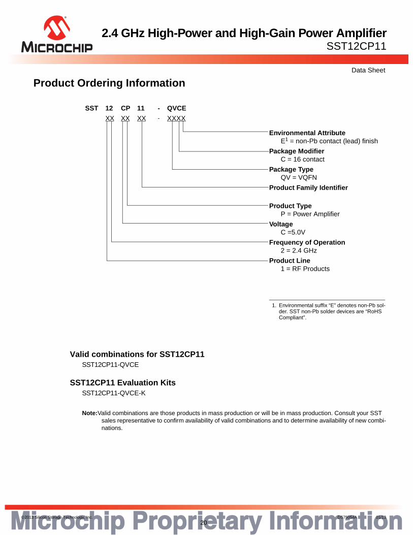
Product Ordering Information
Valid combinations for SST12CP11SST12CP11-QVCE
SST12CP11 Evaluation KitsSST12CP11-QVCE-K
Note:Valid combinations are those products in mass production or will be in mass production. Consult your SST sales representative to confirm availability of valid combinations and to determine availability of new combi-nations.
SST 12 CP 11 - QVCE
XX XX XX - XXXX
Environmental AttributeE1 = non-Pb contact (lead) finish
Package ModifierC = 16 contact
Package TypeQV = VQFN
Product Family Identifier
Product TypeP = Power Amplifier
VoltageC =5.0V
Frequency of Operation2 = 2.4 GHz
Product Line1 = RF Products
1. Environmental suffix “E” denotes non-Pb sol-der. SST non-Pb solder devices are “RoHS Compliant”.

Microchip Proprietary Information©2013 Silicon Storage Technology, Inc. DS75054A 01/13
21
2.4 GHz High-Power and High-Gain Power AmplifierSST12CP11
Data Sheet
Packaging Diagrams
Figure 24:16-contact Very-thin Quad Flat No-lead (VQFN)SST Package Code: QVC
Note: 1. Complies with JEDEC JEP95 MO-220J, variant VEED-4 except external paddle nominal dimensions. 2. From the bottom view, the pin #1 indicator may be either a 45-degree chamfer or a half-circle notch. 3. The external paddle is electrically connected to the die back-side and possibly to certain VSS leads. This paddle can be soldered to the PC board; it is suggested to connect this paddle to the VSS of the unit. Connection of this paddle to any other voltage potential can result in shorts and/or electrical malfunction of the device. 4. Untoleranced dimensions are nominal target dimensions. 5. All linear dimensions are in millimeters (max/min).
16-vqfn-3x3-QVC-2.0
1.7
0.5 BSC
See notes2 and 3
Pin #1
0.300.18
0.075
1.7
0.2
0.05 Max 0.450.35
1.000.80
Pin #1
TOP VIEW BOTTOM VIEWSIDE VIEW
1mm
3.00± 0.075
3.00± 0.075

Microchip Proprietary Information©2013 Silicon Storage Technology, Inc. DS75054A 01/13
22
2.4 GHz High-Power and High-Gain Power AmplifierSST12CP11
Data Sheet
Table 6:Revision History
Revision Description Date
00 • Initial release of data sheet Mar 2009
01 • Added low-power linearity improvement. Updated Features, “Electrical Specifications”, and Figures 3, 14, 15, 16, 17, 18, 19, and 22.
Oct 2009
A • Applied new document format• Released document under letter revision system• Updated Spec number from S71403 to DS75054• Added Figures 4-13 and 23• Updated Figures 14, 16-17• Revised order in which information was presented
Jan 2013
© 2013 Silicon Storage Technology, Inc–a Microchip Technology Company. All rights reserved.
SST, Silicon Storage Technology, the SST logo, SuperFlash, MTP, and FlashFlex are registered trademarks of Silicon Storage Tech-nology, Inc. MPF, SQI, Serial Quad I/O, and Z-Scale are trademarks of Silicon Storage Technology, Inc. All other trademarks and registered trademarks mentioned herein are the property of their respective owners.
Specifications are subject to change without notice. Refer to www.microchip.com for the most recent documentation. For the most current package drawings, please see the Packaging Specification located at http://www.microchip.com/packaging.
Memory sizes denote raw storage capacity; actual usable capacity may be less.
SST makes no warranty for the use of its products other than those expressly contained in the Standard Terms and Conditions of Sale.
For sales office locations and information, please see www.microchip.com.
Silicon Storage Technology, Inc.A Microchip Technology Company
www.microchip.com
ISBN:978-1-62076-906-5
Related Documents