Data Caches for Superscalar Processors* Toni Juan Juan J. Navarro Olivier Temam antoniojQx.upc.es juanjoQac.upc.es [email protected] Dept. Arquitectura de Computadors - Barcelona PRiSM [Jniversitat Politecnica de Catalunya Versailles University Spain FlWlCe Abstract As the number of instructions executed in parallel increases, superscalar processors will require higher bandwidth from data caches. Because of the high cost of true multi-ported caches, alternative cache designs must be evaluated. The purpose of this study is to examine the data cache band- width requirements of high-degree superscalar processors, and investigate alternative solutions. The designs studied range from classic solutions like multi-banked caches to more complex solutions recently proposed in the literature. The performance tradeoffs of these different cache designs are examined in details. Then, using a chip area cost model, all solutions are compared with respect to both cost and performance. While many cache designs seem capable of achieving high cache bandwidth, the best cost/performance t,radeoff varies significantly depending on the dedicated area cost, ranging from multi-banked cache designs to hybrid multi-banked/multi-ported caches or even true multi-ported caches. For instance, we find that an 8-bank cache with mi- nor optimizations perform 10% better than a true a-port cache at half the cost, or that a 4-bank 2 ports per bank cache performs better than a true 4-port cache and uses 45% less chip area. 1 Introduction Currently, processor performance is improved through higher clock rates and increasing the number of instructions ex- ecuted in parallel. This latter trend raises several issues, among which is the necessity to design data and instruc- tion caches which can tolerate several accesses per cycle. Most processors now achieve high throughput with instruc- tion caches by loading one or several cache lines at the same time, thus exploiting instruction stream spatial locality. To a large extent, the effect of branches on instruction stream locality can be hidden by using branch prediction to drive in- struction prefetching [YMP93]. Multiple-access data caches *This work was partly funded by CNRS under a grant from PRC GdR ANM and by the Ministry of Education and Culture of Spain undrr grant CICYT TIC-O-129/95 Copyright 1997 ACM O-8979l-902s5/97/7..$3.50 are more difficult to design because load/store requests sent in parallel share no obvious locality properties. The diffi- culty is to propose a design that can cope with increasing degree of instruction parallelism. The solutions presently implemented in processors can be classified as: l True multi-porting. With respect to performance true multi-porting is clearly an ideal solution, but its chip area cost is high. Cost can be partly reduced by accepting a certain degradation of cache access time that would reduce the performance. . Multiple Cache Copies. For n accesses, the cache must be replicated n times with no benefit to storage space. More- over, store requests are sent simultaneously to all cache copies for coherence and thus no other cache request can be sent in parallel. Since about 30% of memory accesses are store requests [HP96], this solution is severely limited. The DEC 21164 [Dig941 has a dual-ported cache implemented with two copies of the cache array. l Virtual Multiporting. In the Power2 [Mic93], virtual dual-porting is used: the cache SRAM is twice as fast as the processor clock allowing two processor requests in a single processor cycle. The new Alpha 21264 [Dig961 also uses this technique. Again, it is unlikely a cache SRAM n times as fast as the processor clock can become a standard solution. l Multi-banking. The cache is divided in several banks, each bank can be accessed independently of the others. The cost of multi-banking is a crossbar to route requests from load/store units to cache banks and another one from banks back to ports. The crossbar area size as well as the cache access time increase with the number of banks. However, the main issue are the bank conflicts as shows the experi- ence of multi-banked memories in vector processors [OL85]. Bank conflicts occur when two or more requests need to ac- cess the same bank simultaneously. While bank conflicts could be partially eliminated by using a very large num- ber of memory banks in vector processors (512 in the Hi- tachi S-3800 [KISs94]), this solution may not be practical for caches. Increasing the number of banks also implies deeper crossbar and thus longer cache access time, even though smaller banks are faster and could partially compen- sate for cache access time degradation. The Pentium data cache [Int93] has 8 banks, while the MIPS R8000 [MIP94] uses a dual-banked data cache. Thus, to design a data cache that can accept multiple requests simultaneously there are many cost/performance tradeoffs to address. The purpose of this study is to ex- pose these tradeoffs for different cache structures and to provide performance hints for each structure. In Section 2 the superscalar processor architecture used in this study is 60

Welcome message from author
This document is posted to help you gain knowledge. Please leave a comment to let me know what you think about it! Share it to your friends and learn new things together.
Transcript

Data Caches for Superscalar Processors*
Toni Juan Juan J. Navarro Olivier Temam antoniojQx.upc.es juanjoQac.upc.es [email protected]
Dept. Arquitectura de Computadors - Barcelona PRiSM
[Jniversitat Politecnica de Catalunya Versailles University
Spain FlWlCe
Abstract
As the number of instructions executed in parallel increases, superscalar processors will require higher bandwidth from data caches. Because of the high cost of true multi-ported caches, alternative cache designs must be evaluated. The purpose of this study is to examine the data cache band- width requirements of high-degree superscalar processors, and investigate alternative solutions. The designs studied range from classic solutions like multi-banked caches to more complex solutions recently proposed in the literature. The performance tradeoffs of these different cache designs are examined in details. Then, using a chip area cost model, all solutions are compared with respect to both cost and performance. While many cache designs seem capable of achieving high cache bandwidth, the best cost/performance t,radeoff varies significantly depending on the dedicated area cost, ranging from multi-banked cache designs to hybrid multi-banked/multi-ported caches or even true multi-ported caches. For instance, we find that an 8-bank cache with mi- nor optimizations perform 10% better than a true a-port cache at half the cost, or that a 4-bank 2 ports per bank cache performs better than a true 4-port cache and uses 45% less chip area.
1 Introduction
Currently, processor performance is improved through higher clock rates and increasing the number of instructions ex- ecuted in parallel. This latter trend raises several issues, among which is the necessity to design data and instruc- tion caches which can tolerate several accesses per cycle. Most processors now achieve high throughput with instruc- tion caches by loading one or several cache lines at the same time, thus exploiting instruction stream spatial locality. To a large extent, the effect of branches on instruction stream locality can be hidden by using branch prediction to drive in- struction prefetching [YMP93]. Multiple-access data caches
*This work was partly funded by CNRS under a grant from PRC GdR ANM and by the Ministry of Education and Culture of Spain undrr grant CICYT TIC-O-129/95
Copyright 1997 ACM O-8979l-902s5/97/7..$3.50
are more difficult to design because load/store requests sent in parallel share no obvious locality properties. The diffi- culty is to propose a design that can cope with increasing degree of instruction parallelism. The solutions presently implemented in processors can be classified as:
l True multi-porting. With respect to performance true multi-porting is clearly an ideal solution, but its chip area cost is high. Cost can be partly reduced by accepting a certain degradation of cache access time that would reduce the performance.
. Multiple Cache Copies. For n accesses, the cache must be replicated n times with no benefit to storage space. More- over, store requests are sent simultaneously to all cache copies for coherence and thus no other cache request can be sent in parallel. Since about 30% of memory accesses are store requests [HP96], this solution is severely limited. The DEC 21164 [Dig941 has a dual-ported cache implemented with two copies of the cache array.
l Virtual Multiporting. In the Power2 [Mic93], virtual dual-porting is used: the cache SRAM is twice as fast as the processor clock allowing two processor requests in a single processor cycle. The new Alpha 21264 [Dig961 also uses this technique. Again, it is unlikely a cache SRAM n times as fast as the processor clock can become a standard solution.
l Multi-banking. The cache is divided in several banks, each bank can be accessed independently of the others. The cost of multi-banking is a crossbar to route requests from load/store units to cache banks and another one from banks back to ports. The crossbar area size as well as the cache access time increase with the number of banks. However, the main issue are the bank conflicts as shows the experi- ence of multi-banked memories in vector processors [OL85]. Bank conflicts occur when two or more requests need to ac- cess the same bank simultaneously. While bank conflicts could be partially eliminated by using a very large num- ber of memory banks in vector processors (512 in the Hi- tachi S-3800 [KISs94]), this solution may not be practical for caches. Increasing the number of banks also implies deeper crossbar and thus longer cache access time, even though smaller banks are faster and could partially compen- sate for cache access time degradation. The Pentium data cache [Int93] has 8 banks, while the MIPS R8000 [MIP94] uses a dual-banked data cache.
Thus, to design a data cache that can accept multiple requests simultaneously there are many cost/performance tradeoffs to address. The purpose of this study is to ex- pose these tradeoffs for different cache structures and to provide performance hints for each structure. In Section 2 the superscalar processor architecture used in this study is
60
described, its performance, cache bandwidth requirements and the characteristics of its cache requests are analyzed in Section 3. True multi-ported caches are examined in Sec- t,ion 4 a.nd these results are used as performance references t.hroughout, t.he study. Multi-banked caches are examined in Section 5, and several alternative designs to both multi- ported and multi-banked caches are discussed in Section 6. These different solutions are first compared in terms of per- formance throughout the study, and in Section 7 the area cost model developed by Mulder et al. [MQFSl] is used to determine the best overall cost/performance tradeoffs. Fi- nally, Section 8 presents some related work.
2 Methodology
As processor issue rate increases and the sustained number of instructions executed per cycle (IPC) is closer to the peak IPC, t#he number of memory requests per cycle is naturally going to increase. To mimic this increased processor pres- sure on data caches, we have used a superscalar processor with high issue rate. As issue rate increases, more sophisti- cated branch prediction techniques and a larger number of functional units can be expected. Though it is feasible to add functional units, elaborating on future branch predic- tion t#echniques is out of the scope of this article. To still take these future improvements into account and also to ex- hibit maximal data cache pressure, we have removed these two processor bottlenecks by using perfect branch prediction and a large number of functional units. We acknowledge these assumptions affect the data address trace. Mainly the distribution of data cache requests over time (which cache requests are sent in the same cycle) is changed, but the ad- dress sequence is less affected since instruction dependencies are considered. Inspite of the imprecision, we still find this tracing methodology to be the best tradeoff for obtaining high data cache pressure and an accurate address trace. A similar approach of using perfect branch prediction was used in a recent study by Jourdan et al. [JSL95] which aimed at dimensioning functional units of future superscalar proces- sors.
Simulated Architecture
We defined a processor architecture close to that of the HP- 8000 which we found to be both aggressive at extracting ILP and simple enough to scale up well.’ Present processors is- sue 4 to 6 instructions per cycle. We found that increasing processor degree beyond 8 does not bring significant im- provements for most codes. So, except for this section, we use a degree 8 processor. Like the HP-8000, the processor architecture includes an instruction queue playing the role of both reservation stations and commit buffer.’ Instruc- tions are sent in-order to the queue, dispatched to functional units, executed out-of-order, and committed in-order again. Commits are performed in-order to preserve the coherence of store requests, enable easy squashing of instructions and recovery after exceptions. The instruction queue is split into a load/store queue and a scalar instruction queue as in the HP-8000. A scalar instruction queue entry contains operands and/or sources of operands (functional units iden- tifiers). The load/store queue contains the same information plus the data address. This address is used to maintain co- herence between load/store instructions. A load can be sent
‘The HP-8000 is a superscalar processor of degree 4. 2Tl,,s Instruction queue corresponds to the znstructzon wndow
rnerkoned above and in [JSL95]
t,o cache only if the addresses of all older store instructions are knowu and distinct. If there exists a store with same ad- dress, the load is not sent to cache and the data is directly read from the load/store queue. Stores execute only when they retire. The main processor parameters are the num- ber of instructions fetched together, i.e., the degree of the superscalar processor, the number of instructions the pro- cessor attempts to commit every cycle, the functional units configuration (number, types, latencies and issue rates) and the instruction window size (the size corresponds to the sum of the load/store queue size and the scalar queue size; both queues have identical size). To restrict the number of com- binations, several configurations have been defined which correspond to different scales of the same design, see Ta- ble 1. In Section 3, all configurations are used, but in the other sections, only configuration 2 is used.
configuration 1 2 3 4
Degree Nb. of inst. 4 8 16 32 fetched per cycle) Nb of inst. attempted 4 8 16 32 to be committed per cycle Instruction window size 1 64 128 256 512
Table 1: Processor Configurations.
As mentioned above, we assume perfect instruction fetch. To reduce the impact of resource conflicts on processor per- formance, the number of functional units of each type is equal to the processor degree for each configuration. The functional units latencies are 1 cycle for all ALU operations, 2 cycles for floating-point ADD, 4 cycles for floating-point MULT and 20 cycles for floating-point DIV. All functional units are fully pipelined except for floating-point DIV.
Cache memory parameters
In the next sections, we seek to define and dimension cache designs that can cope with such processor architectures. A few cache/memory parameters remain fixed. In this study, we essentially consider a fast first-level on-chip data cache. Since cache access time is one of our main concerns, the cache is direct-mapped. The cache is also write-back, write- allocate. The cache size is equal to 32 Kbytes, i.e., within the current range of 8 Kbytes to 256 Kbytes, and the line size is equal to 32 bytes. This cache configuration is called the Baseline cache throughout the text and figures. Unless otherwise mentioned, the cache is non-blocking. The miss latency to the next memory level is 5 cycles, the access to this lower memory level is pipelined and one miss request can be sent every cycle with at most 5 pending requests, i.e., as if a close second-level cache is used. However, this lower memory level is not simulated and all requests are considered hits to restrict the number of parameters and focus on the first-level cache.
In the remainder of the text it is necessary to distin- guish between the number of processor-to-cache ports which corresponds to the number of data paths between the pro- cessor and the cache, and the number of cache ports or cell ports which corresponds to the number of ports of each cache SRAM cell. An n-bank cache may have only p processor- to-cache ports with p < n. For example, the Pentium data cache [IntYS] has 2 processor-to-cache ports, 8 banks and 1 cell port, i.e., n = 8 and p = 2. It is assumed that a
61

y-port ca.che is always associated with a processor having p processor-to-cache ports.
Benchmarks
Ten benchmarks were used for the study, five SPECint92 codes and five SPECfp92 codes listed in Table 2. SPEC92 was preferred over SPEC95 because simulation time restricts trace length. With SPEC95, a small trace length is likely to only correspond to a very small fraction of the whole code. Since this study is focused on bandwidth rather than la- tency, having representative ILP performance, i.e., travers- ing many different code constructs, was considered more im- portant than having large data sets. No particular criterion drove the selection of these SPEC92 benchmarks. We picked the five first SPECfp92 and SPECint92 that ran success- fully with Spy [G. 911, the tracer used in this study. For each benchmark, 100-million instruction traces were simu- lated which correspond to 5%-10% of most benchmarks. The first 10 million instructions were ignored. Benchmarks were compiled on Sun Spare processors using -04 optimization. No software optimization is used to exhibit more ILP except for loop unrolling as provided in the Sun compilers.
hydro2d 0.72 1.95 2.06 2.09 2.10 42% 0.07 Avg FP 0 91 1.91 2.06 2.13 214 32% 0.07 espresso 1.00 3.74 5.75 7.14 7.75 25% 0.01 Ii 0.89 4.00 7.15 8.03 8.09 31% 0.01 eqntott 0.95 3.91 6.85 9.26 11.0 23% 0.03 compress 0.64 3.85 4.88 5.00 5.02 23% 0.16 IFC 0.77 3.46 5.01 5.74 6.04 28% 0.02 Avg INT 0.85 3.79 5.93 7.03 7.58 26% 0.05
Avg All 0.88 2.85 3.99 4.58 4.85 29% 0.06 Mem IPC NA 0.79 1.11 1.25 1.31 N.A N.A
Table 2: Alpha 2116.4 IPC, IPC with perfect cache for dif- ferent super-scalar degrees, Percentage of memory operations in each benchmark and Miss Ratio with the baseline cache.
3 Performance Thresholds and Nature of Cache Requests
In order to get a performance bound for our superscalar pro- cessor, simulations were first run for each of the 10 bench- marks assuming a perfect cache, i.e., no cache miss and unlimited number of cache ports, so that each load/store reference is serviced in a single cycle. Table 2 shows the performance measured in instructions committed per cycle, denoted IPC (Instruction Per Cycle), for the four differ- ent processor configurations with a perfect cache. The best average IPC is equal to 4.85 for a processor of degree 32. Though this figure is not so high, the actual sustained IPC of current processors is much lower. In [CB96], the IPC of the Alpha 21164 for the same benchmarks were collected and are shown in Table 2. The Alpha 21164 is a 4-way issue processor and it achieves an average IPC of 0.88 for the selected benchmarks. Therefore, even if the IPC for the MIPS RlOOOO or the HP 8000, which use out-of-order exe- cution unlike the DEC 21164, are 2 or 3 times higher, these results show that significantly higher IPC can be achieved with higher issue rate under optimal hypotheses (perfect
3i
Figure 1: Distribution of Number of Cache Requests Sent
Simultaneously (cumulated) with perfect cache.
branch prediction, no resource conflict). Also, the best av- erage floating-point IPC (2.14) is lower than the best av- erage integer IPC (7.58). Because branch prediction is one of the major bottlenecks of integer codes, it is natural that using perfect branch prediction boosts integer codes perfor- mance. These numbers do not reflect the theoretical in- trinsic instruction-level parallelism indicated in [HP961 but they are consistent with the detailed experiments by Jour- dan et al. [JSL95]: about 7.5 IPC for integer codes and about 4.5 for floating-point codes in average 3. Though floating- point IPC is also lower than integer IPC in the latter study, we observed lower floating-point IPC but we used a different instruction set: Spare processor and code compiled on a Su- persparc 20 while Jourdan et al. used the MIPS instruction set compiled on a R4600 SGI. Table 2 also provides the miss ratio of the benchmarks with the baseline cache (32-Kbyte cache and 32-byte line). Finally, in table 2, the percent- age of load/store requests of each benchmark is indicated to get a hint at the average number of memory requests sent per cycle. Because the average IPC is bounded by 4.85 even when 32 instruction slots and a window size of 512 are used,4 the average number of load/store requests per cycle, i.e., memory IPC, remains bounded by 1.31. However, cache performance is not only affected by global volume of data transactions but also by the distribution of the number of requests sent simultaneously.
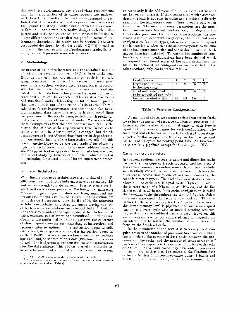
Figure 1 shows the cumulated distribution5 of cache re- quest size, i.e., the number of cache requests sent at the same time. For example, for an 8-degree processor, 45% of cache requests are sent by groups of 4 requests or more. 87% cache requests are sent along with one or more requests for a pro- cessor of degree 8, with a maximum of 93% for a processor of degree 32. It even appears that 25% of load/store requests are sent by blocks larger than 8 for an 8-degree processor, for example. Though a superscalar processor of degree 8 can fetch or commit no more than 8 instructions together, the instruction window has 128 entries in our case. Thus, it is possible to have more than 8 load/store instructions ready to execute in the same cycle. The concentration of requests partly lays in the way instructions are committed. In Figure 2 the non-cumulated distribution6 of the number of instructions committed per cycle is shown. All instruc- tions are considered in this figure. Moreover, cycles where
3A11 the Spec92 benchmarks were used in this study. 4A 512~entry window is unlikely to be implemented. These param-
eters are used to find the upper-bound IPC. 5Note that cycles where no request is sent to cache are not con-
sIdered in this figure 61n this case, the non-cumulated distribution is used to better
highlight its irregularity
62
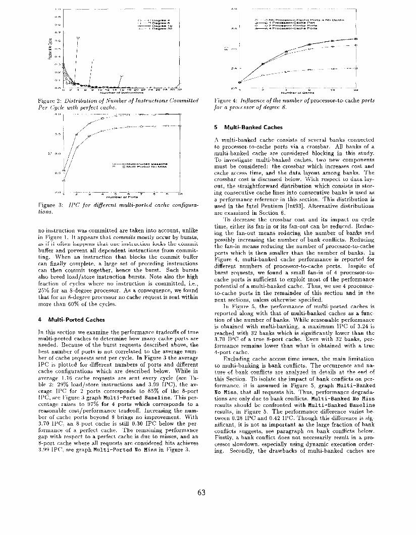
Figure 2: Distribution of Number of Instructions Committed Per Cycle with perfect cache.
4 0 cI m;::..::L-~=~i~--- /= ----I
Figure 3: IPC for difierent multi-ported cache configura- tions.
no instruction was committed are taken into account, unlike in Figure 1. It appears that commits mostly occur by bursts, as if it often happens that one instruction locks the commit buffer and prevent all dependent instructions from commit- ting. When an instruction that blocks the commit buffer can finally complete, a large set of preceding instructions can then commit together, hence the burst. Such bursts also breed load/store instruction bursts. Note also the high fraction of cycles where no instruction is committed, i.e., 25% for an °ree processor. As a consequence, we found that for a.n 8-degree processor no cache request is sent within more than 60% of the cycles.
4 Multi-Ported Caches
In this section we examine the performance tradeoffs of true multi-ported caches to determine how many cache ports are needed. Because of the burst requests described above, the best number of ports is not correlated to the average num- ber of cache requests sent per cycle. In Figure 3 the average IPC is plotted for different numbers of ports and different cache configurations which are described below. While in average 1.16 cache requests are sent every cycle (see Ta- ble 2: 29% load/store instructions and 3.99 IPC), the av- erage IPC for 2 ports corresponds to 85% of the 8-port IPC, see Figure 3 graph Multi-Ported Baseline. This per- centage raises to 97% for 4 ports which corresponds to a reasonable cost/performance tradeoff. Increasing the num- ber of cache ports beyond 8 brings no improvement. With 3.70 IPC, an &port cache is still 0.30 IPC below the per- formance of a perfect cache. The remaining performance gap with respect to a perfect cache is due to misses, and an S-port cache where all requests are considered hits achieves 3.99 IPC, see graph Multi-Ported No Miss in Figure 3.
Figure 4: Influence of the number of processor-to-cache ports
jor a processor of degree 8.
5 Multi-Banked Caches
A multi-banked cache consists of several banks connected to processor-to-cache ports via a crossbar. All banks of a multi-banked cache are considered blocking in this study. To investigate multi-banked caches, two new components must be considered: the crossbar which increases cost and cache access time, and the data layout among banks. The crossbar cost is discussed below. With respect to data lay- out, the straightforward distribution which consists in stor- ing consecutive cache lines into consecutive banks is used as a performance reference in this section. This distribution is used in the Intel Pentium [Int93]. Alternative distributions are examined in Section 6.
To decrease the crossbar cost and its impact on cycle time, either its fan-in or its fan-out can be reduced. Reduc- ing the fan-out means reducing the number of banks and possibly increasing the number of bank conflicts. Reducing the fan-in means reducing the number of processor-to-cache ports which is then smaller than the number of banks. In Figure 4, multi-banked cache performance is reported for different numbers of processor-to-cache ports. Inspite of burst requests, we found a small fan-in of 4 processor-to- cache ports is sufficient to exploit most of the performance potential of a multi-banked cache. Thus, we use 4 processor- to-cache ports in the remainder of this section and in the next sections, unless otherwise specified.
In Figure 5, the performance of multi-ported caches is reported along with that of multi-banked caches as a func- tion of the number of banks. While reasonable performance is obtained with multi-banking, a maximum IPC of 3.24 is reached with 32 banks which is significantly lower than the 3.70 IPC of a true &port cache. Even with 32 banks, per- formance remains lower than what is obtained with a true 4-port cache.
Excluding cache access time issues, the main limitation to multi-banking is bank conflicts. The occurrence and na- ture of bank conflicts are analyzed in details at the end of this Section. To isolate the impact of bank conflicts on per- formance, it is assumed in Figure 5, graph Multi-Banked No Miss, that all requests hit. Thus, performance degrada- tions are only due to bank conflicts. Multi-Banked No Miss results should be confronted with Multi-Banked Baseline results, in Figure 5. The performance difference varies be- tween 0.28 IPC and 0.42 IPC. Though this difference is sig- nificant, it is not as important as the large fraction of bank conflicts suggests, see paragraph on bank conflicts below. Firstly, a bank conflict does not necessarily result in a pro- cessor slowdown, especially using dynamic execution order- ing. Secondly, the drawbacks of multi-banked caches are
63
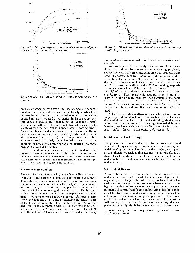
Figure 6: Distribution OS number of simultaneous requests to u bank.
partly compensated by a few minor assets. One of the main point is that multi-banked caches are naturally non-blocking because banks operate in a decoupled manner. Thus, a miss in one bank does not stall other banks. In Figure 5, the per- formance of blocking multi-banked caches (Baseline graph) is compared with non-blocking multi-banked caches (up to 5 outstanding misses) Multi-Banked Non-Blocking graph. As the number of banks increases, the number of simultane- ous misses that can occur in a blocking multi-banked cache also increases (one per bank), and thus performance differ- ence tends to 0. Similarly, multi-banked caches with large numbers of banks are better capable of limiting the cache bandwidth wasted by writes.
The second main performance bottleneck of multi-banked caches is crossbar routing delay. In order to examine the impact of crossbar on performance, several simulations were run where cache access time is increased by one or two cy- cles. The results are reported in [JNT96].
Nature of bank conflicts
Bank conflicts are shown in Figure 6 which indicates the dis- tribution of the number of simultaneous requests to a bank. These statistics have been collected by counting each cycle the number of cache requests in the load/store queue which are both rea.dy to execute and mapped to the same bank; these statistics were averaged over all banks. For instance with 4 ba.nks, 28% of requests never experience bank con- flicts, 18% conflict with another request, 12% conflict with two other requests,. and the remaining 42% conflict with at, least 3 other requests. The number of conflicts is very high, see Figure 6, starting with 81% of requests experienc- ing a conflict in a 2-bank cache, and still more than 60% in a 16-bank or 32-bank cache. Past 16 banks, increasing
Figure 7: Distribution of number of distinct lines conflicting requests.
among
the number of banks is rather inefficient at removing bank conflicts.
We now wish to further analyze the nature of bank con- flicts. Spatial locality suggests consecutive many closely spaced requests can target the same line and thus the same bank. To determine what fraction of conflicts correspond to requests to the same line, the distribution of the number of distinct lines among conflicting requests is reported in Fig- ure 7. For instance with 4 banks, 71% of pending requests target the same line. This result should be confronted to the 28% of requests which do not conflict in a 4-bank cache, see Figure 6. This means 43% requests experienced con- flicts with one or more requests that referenced the same line. This difference is still equal to 43% for 32 banks. Also, Figure 7 indicates there are few cases where 3 distinct lines are involved in a bank conflict when 4 or more banks are used.
Not only multiple simultaneous requests to banks occur frequently, but we also found that conflicts are not evenly distributed over banks, certain banks standing significantly more stress than others with an average fourfold difference between the bank with fewest conflicts and the bank with most conflicts for an a-bank cache (27% versus 7%).
6 Alternative Cache Designs
The previous sections were dedicated to the two most straight- forward techniques for improving data cache bandwidth, i.e., multi-porting and multi-banking. In this section, we explore several alternative designs that attempt to address the main flaws of each solution, i.e., cost and cache access time for multi-porting or bank conflicts and cache access time for multi-banking.
6.1 Hybrid Design
A first alternative is a combination of both designs i.e., a multi-banked cache where each bank has several ports. Us- ing multiple banks provides additional bandwidth at a low cost, and multiple ports help removing bank conflicts. Fix- ing the number of processor-to-cache port to 4,7 the per- formance of several bank/port configurations has been mea- sured for 1,2,4 and 8 banks and is reported in Figure 8 as a function of the number of ports per bank. The banks are here considered non-blocking for the sake of comparison with multi-ported caches. We find that a true 4-port cache performs only slightly better than a 4-bank ‘L-port cache.
7More exactly, we use mzn(4,number of banks x num- be? o.f ports per bank).
64
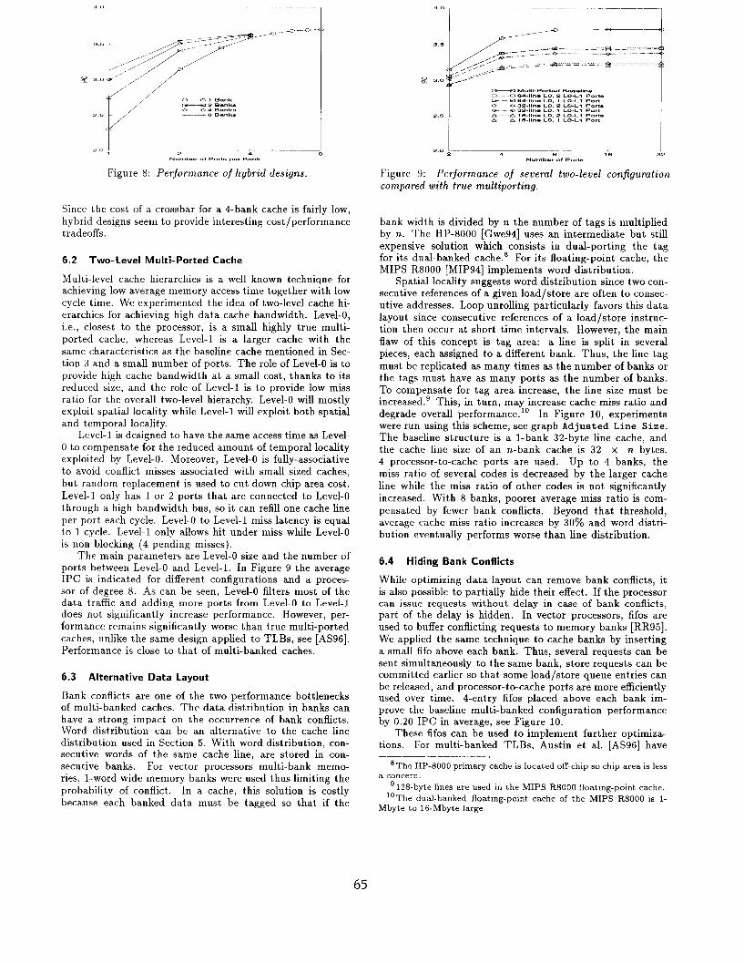
Since the cost of a crossbar for a 4-bank cache is fairly low, hybrid designs seem to provide interesting cost/performance tradeoffs.
6.2 Two-Level Multi-Ported Cache
Multi-level cache hierarchies is a well known technique for achieving low average memory access time together with low cycle time. We experimented the idea of two-level cache hi- erarchies for achieving high data cache bandwidth. Level-O, i.e., closest to the processor, is a small highly true multi- ported cache, whereas Level-l is a larger cache with the same characteristics as the baseline cache mentioned in Sec- tion 3 and a small number of ports. The role of Level-O is to provide high cache bandwidth at a small cost, thanks to its reduced size, and the role of Level-l is to provide low miss ratio for the overall two-level hierarchy. Level-O will mostly exploit spatial locality while Level-l will exploit both spatial and temporal locality.
Level-l is designed to have the same access time as Level- 0 to compensate for the reduced amount of temporal locality exploited by Level-O. Moreover, Level-O is fully-associative to avoid conflict misses associated with small sized caches, but random replacement is used to cut down chip area cost. Level-l only has 1 or 2 ports that are connected to Level-O through a high bandwidth bus, so it can refill one cache line per port each cycle. Level-O to Level-l miss latency is equal to 1 cycle. Level-l only allows hit under miss while Level-O is non-blocking (4 pending misses).
The main parameters are Level-O size and the number of ports between Level-O and Level-l. In Figure 9 the average IPC is indicated for different configurations and a proces- sor of degree 8. As can be seen, Level-O filters most of the data traffic and adding more ports from Level-O to Level-l does not significantly increase performance. However, per- formance remains significantly worse than true multi-ported caches, unlike the same design applied to TLBs, see [AS96]. Performance is close to that of multi-banked caches.
6.3 Alternative Data layout
Bank conflicts are one of the two performance bottlenecks of multi-banked caches. The data distribution in banks can have a strong impact on the occurrence of bank conflicts. Word distribution can be an alternative to the cache line distribution used in Section 5. With word distribution, con- secutive words of the same cache line, are stored in con- secutive banks. For vector processors multi-bank memo- ries, l-word wide memory banks were used thus limiting the probability of conflict. In a cache, this solution is costly because each banked data must be tagged so that if the
2.0 , -~~~~~ --2 I 2 4 r-dmk...:o, ,e 32
PO”.
Figure 9: Performance of several two-level configuration compared with true multiporting.
bank width is divided by n the number of tags is multiplied by n. The HP-8000 [Gwe94] uses an intermediate but still expensive solution which consists in dual-porting the tag for its dual-banked cache.’ For its floating-point cache, the MIPS R8000 [MIP94] implements word distribution.
Spatial locality suggests word distribution since two con- secutive references of a given load/store are often to consec- utive addresses. Loop unrolling particularly favors this data layout since consecutive references of a load/store instruc- tion then occur at short time intervals. However, the main flaw of this concept is tag area: a line is split in several pieces, each assigned to a different bank. Thus, the line tag must be replicated as many times as the number of banks or the tags must have as many ports as the number of banks. To compensate for tag area increase, the line size must be increased.g This, in turn, may increase cache miss ratio and degrade overall performance.” In Figure 10, experiments were run using this scheme, see graph Adjusted Line Size. The baseline structure is a l-bank 32-byte line cache, and the cache line size of an n-bank cache is 32 x n bytes. 4 processor-to-cache ports are used. Up to 4 banks, the miss ratio of several codes is decreased by the larger cache line while the miss ratio of other codes is not significantly increased. With 8 banks, poorer average miss ratio is com- pensated by fewer bank conflicts. Beyond that threshold, average cache miss ratio increases by 30% and word distri- bution eventually performs worse than line distribution.
6.4 Hiding Bank Conflicts
While optimizing data layout can remove bank conflicts, it is also possible to partially hide their effect. If the processor can issue requests without delay in case of bank conflicts, part of the delay is hidden. In vector processors, fifos are used to buffer conflicting requests to memory banks [RR95]. We applied the same technique to cache banks by inserting a small fifo above each bank. Thus, several requests can be sent simultaneously to the same bank, store requests can be committed earlier so that some load/store queue entries can be released, and processor-to-cache ports are more efficiently used over time. 4-entry fifos placed above each bank im- prove the baseline multi-banked configuration performance by 0.20 IPC in average, see Figure 10.
These fifos can be used to implement further optimiza- tions. For multi-banked TLBs, Austin et al. [AS961 have
‘The HP-8000 primary cache is located off-chip so chip area is less a concern.
‘128-byte lines are used in the MIPS R8000 floating-point cache. “The dual-banked floating-point cache of the MIPS R8000 is l-
Mbyte to 16-Mbyte large.
65

Figure 10: Performance of conflict hiding techniques.
proposed to compare pending TLB requests because of bank conflicts to the request currently processed by the bank. When this request completes, all matching pending requests use the result and complete simultaneously. We have eval- uated a similar design for multi-banked caches using the fifo placed above each bank. One or several fifo entries can be compared to the address of the request in process. Wilson et al. [WOR96] have proposed a similar scheme for single-banked caches where multiple pending requests can be checked against the request in process. Such schemes can only remove conflicts between requests to the same cache line but, in Section 5, we show that such conflicts correspond to a significant share of all bank conflicts. The design cost essentially depends on the number of fifo entries that can be simultaneously compared to the request processed by the bank (1 up to 4 in our case). Performance for 1 and 4 simul- taneous comparisons are indicated in Figure 10 (4 processor- to-cache ports). Hiding same-line conflicts brings an overall performance improvement of 0.15 IPC, i.e., about half the performance difference between a true 8-port cache and a 32-bank cache. Hiding bank conflicts reduces the number of banks necessary to achieve reasonable performance and thus lessens cache access time degradations.
7 A Cost/Performance Comparison
One the main motivations for this work is the prohibitive cost of true multi-ported caches. After examining the per- formance of several alternative designs, we wish to show that, for a given transistor count, some of these alterna- tives provide better performance than true multi-porting. For that purpose, we use the area model for on-chip mem- ories by Mulder et al. [MQFSl] where each cache memory component cost is measured in register-bit equivalent (rbe) cells. This is a technology-independent metric correspond- ing to a 6-transistor static area cell with high bandwidth. A single such 6-transistor SRAM cell has a cost of 0.6 rbe. The rbe of control logic, comparators, sense amplifiers and all other basic blocks is also provided. Layout and aspect ratio are assumed to have no effect on area count. Though this is an approximation, we believe that the layout impact can be made similar for all proposed designs and thus can be ignored. Moreover, the area model is used to sort cache designs according to the area cost and not to compute an accurate area cost value.
In Figure 11 the relative cost/performance of most cache designs evaluated in this study is plotted. The x-axis cor- responds to the relative cost with respect to baseline cache (1 port, 1 bank), and the y-axis to the IPC. The x-axis uses a logarithmic scale. Each category of design is associated with a character reported in the legend (P for multi-ported
4.0 -
Figure 11: C’ost/Yerformance tradeoffs between different cache designs.
for instance), and the number next to this character is the design configuration. This number corresponds to the num- ber of banks for all designs, except for Multi-Port where it corresponds to the number of ports, and for Two-Level where it corresponds to the number of Level-O ports.
95% of the maximal performance is achieved with an 8- bank cache using same-line optimization, see Section 6.4. On the other hand standard multi-bank caches usually do not represent a good cost/performance tradeoff. Hybrid de- signs perform well but for comparable performance their cost is usually two times that of a multi-bank design with conflict optimizations. None of the design studied can reach more than 95% of the performance of true multi-ported caches. However, many designs can achieve 75% or more of the max- imal performance at a very small cost. For instance a 2-bank cache using fifos above each bank reaches 75% of the max- imal performance with only a 10% area overhead. Other designs like two-level caches perform well but for a narrow interval of performance: to get 90% of the maximal perfor- mance, a two-level hierarchy with an 8-port Level-O cache represents the best cost/performance tradeoff.
In Figure 11, it was assumed the same cycle time can be achieved for all designs. In [JNT96], some experiments introduce delay cycles and can be used to determine a more accurate order of each design.
8 Related Work
While many studies have dealt with improving memory hi- erarchy performance, most have focused on memory latency issues. This trend is now changing, with several recent stud- ies dealing with cache bandwidth issues. Sohi et al. [SF911 evaluated non-blocking caches as a means to increase mem- ory hierarchy bandwidth. They also suggest multi-ported, duplicate or inter-leaved caches as solutions to cache band- width issues, but do not evaluate these different solutions in details. Burger et al. [BKG96] have isolated the respective impact of latency and bandwidth on global memory hier- archy performance, concluding cache bandwidth is a major performance issue in current superscalar processors. They further outline that latency tolerating techniques can de- grade cache bandwidth. Wilson et al. [WOR96] have pro- posed and evaluated several mechanisms to obtain more than one memory access per cycle from a single cache port
66
using buffering techniques to increasing port width. Their motivation also lays in the prohibitive cost of multiported caches, with respect to both area cost and cache access time. Finally, Austin et al. [AS961 examine in details several TLB designs for physically tagged caches that can achieve high bandwidt,h. Though most of these designs were also exam- ined in the present study, conclusions diverge significantly because cache and TLB locality properties are different.
9 Conclusions and Future Work
In this paper, several techniques for improving data cache bandwidth have been evaluated. Because of the prohibitive cost of multi-ported SRAM cells, most designs based on this technique, i.e., true multi-ported caches, two-level caches with highly multi-ported first-level cache or hybrid designs (multi-bank + multi-port) are usually too costly for the performance obtained. Best solutions are based on multi- banked caches. Raw multi-banked caches usually perform poorly, but simple hardware enhancements to hide or re- move conflicts can significantly improve overall performance, and the chip overhead for such add-ons is only lo-15% of the raw multi-banked cache cost. Besides deciding the best cost/performance tradeoff for achieving high data cache band- width, these results also provide a hierarchy of the different techniques for improving cache bandwidth, both with re- spect to performance (IPC) and chip area cost.
In this study, the influence of access time was modeled by increasing the cache pipeline length. We intend to use a time model to improve the accuracy of the comparison between the different cache designs. Ultimately, this comparison will be based on three parameters: IPC, cycle time and chip area cost.
References
[AS961 Todd M. Austin and Gurindar S. Sohi. High- bandwidth address translation for multiple-issue pro- cessors. In Proceedings of the ,?3rd ACM International Symposium on Computer Architecture, Philadelphia, May 1996.
[BKGSG] D. Burger, A. K;igi, and J. R. Goodman. Memory bandwidth limitations of future microprocessors. In Proceedings of the L&d ACM International Sympo- sium on Computer Architecture, Philadelphia, May 1996.
[CBS61 Zarka Cvetanovic and Dileep Bhandakar. Performance characterization of the alpha 21164 microprocessor us- ing TP and SPEC wordloads. In Second IEEE Inter- national Symposium on High Performance Computer Architecture, pages 2X-280, San Jose, February 1996.
[Dig941 Digital Equipment Corporation, Maynard, Massachus- sets. Alpha Architecture Handbook, 1994.
[Dig961 Digital Equipment Corporation, Maynard, Massachus- sets. Alpha Architecture Handbook, 1996.
[G. 911 G. Irlam. SPA package, 1991.
[Gwe94] Linley Gwennap. HP-8000 combines complexity and speed. MiCTOpTOCeSSOT Report, 8(15):5-g, November 1994.
[HP961 John L. Hennessy and David A. Patterson. CompzLter Architecture: A Quantitative Approach, 2nd Edition. Morgan Kaufmann Publishers Inc., 1996.
[Int93] Intel. Pentiam Processor User’s Manual, 1993.
[JNTSG] Toni Juan, Juan J. Navarro, and Olivier Temam. Data caches for superscalar processors. Technical Report 96/038, PRISM, Versailles University, December 1996.
[JSL95]
[KIS+94]
[MicQ3]
[MIP94]
[M&F911
[OL85]
[RR951
[SF911
[WOR96]
[YMPSS]
Stephan Jourdan, Pascal Sainrat, and Daniel Litaize. Exploring Configurations of Functional Units in an Out-of-Order Superscalar Processor. In Proceedings oj the 23rd ACM International Symposium on Computer Architecture, pages 117-125, Italy, July 1995.
K. Kitai, T. Isobe, T. Sakakibara, S. Yazawa, Y. Tamaki, T. Tanaka, and K. Ishii. Distributed stor- age control unit for the hitachi s-3800 multivector su- percomputer. In Proceedings of the International Con- ference orz Stipe~compating, pages l-10, Manchester, .Jul 1994.
MicroprocessorReport, ~01.7, no 13. IBM Regains Per- ,formance Lead with Power& October 1993.
MIPS Technologies Incorporated. R8000 Micropro- C~SSOT Chip Set, Product Overview, 1994.
Johannes M. Mulder, Nhon T. Quach, and Michael J. Flynn. An area model for on-chip memories and its application. International Journal of High Speed Com- puting, 26(2):98-106, Feb 1991.
W. Oed and 0. Lange. On the effective bandwidth of interleaved memories in vector processor systems. IEEE TT~TLSaCtiOTLS 0lt 6bTpteTS, c-34(1o):949-957, Ott 1985.
K.A. Robbins and S. Robbins. Buffered banks in multi- processor systems. IEEE Transactions on Computers, 44(4), Apr 1995.
Gurindar S. Sohi and Manoj Franklin. High-bandwidth data memory systems for superscalar processors. In Proceedings of the 4th International Conference on AT- chitectural Support for Programming Languages and Operating Systems, pages 53-62, April 1991.
Kenneth M. Wilson, Kunle Olukotun, and Mendel Rosenblum. Increasing cache port efficiency for dy- namic superscalar microprocessors. In Proceedings of Ihe 23rd ACM International Symposium on Computer Architecture, pages 147-157, Philadelphia, May 1996.
T. Yeh, D. T. Marr, and Y. N. Patt. Increasing the instruction fetch rate via multiple branch predictors and a branch address cache. In Proceedings of the 7th ACM International Conference on Supercompzlt- ing, Jul 1993.
67
Related Documents