® 1. General description The DAC1008D750 is a high-speed 10-bit dual channel Digital-to-Analog Converter (DAC) with selectable 2, 4 or 8 interpolating filters optimized for multi-carrier WCDMA transmitters. Because of its digital on-chip modulation, the DAC1008D750 allows the complex pattern provided through lane 0, lane 1, lane 2 and lane 3, to be converted up from baseband to IF. The mixing frequency is adjusted via a Serial Peripheral Interface (SPI) with a 32-bit Numerically Controlled Oscillator (NCO) and the phase is controlled by a 16-bit register. The DAC1008D750 also includes a 2, 4 or 8 clock multiplier which provides the appropriate internal clocks and an internal regulation to adjust the output full-scale current. The input data format is serial according to JESD204A specification. This new interface has numerous advantages over the traditional parallel one: easy PCB layout, lower radiated noise, lower pin count, self-synchronous link, skew compensation. The maximum number of lanes of the DAC1008D750 is 4 and its maximum serial data rate is 3.125 Gbps. The Multiple Device Synchronization (MDS) guarantees a maximum skew of one output clock period between several DAC devices. MDS incorporates modes: Master/slave and All slave mode. 2. Features and benefits DAC1008D750 Dual 10-bit DAC; up to 750 Msps; 2, 4 or 8 interpolating with JESD204A interface Rev. 04 — 2 July 2012 Product data sheet Dual 10-bit resolution IMD3: 80 dBc; f s = 737.28 Msps; f o = 140 MHz 750 Msps maximum update rate ACPR: 64 dBc; two carriers WCDMA; f s = 737.28 Msps; f o = 153.6 MHz Selectable 2, 4 or 8 interpolation filters Typical 1.26 W power dissipation at 4 interpolation, PLL off and 740 Msps Input data rate up to 312.5 Msps Power-down mode and Sleep modes Very low-noise cap-free integrated PLL Differential scalable output current from 1.6 mA to 22 mA 32-bit programmable NCO frequency On-chip 1.29 V reference Four JESD204A serial input lanes External analog offset control (10-bit auxiliary DACs) 1.8 V and 3.3 V power supplies Internal digital offset control LVDS compatible clock inputs Inverse (sin x) / x function

Welcome message from author
This document is posted to help you gain knowledge. Please leave a comment to let me know what you think about it! Share it to your friends and learn new things together.
Transcript

1. General description
The DAC1008D750 is a high-speed 10-bit dual channel Digital-to-Analog Converter (DAC) with selectable 2, 4 or 8 interpolating filters optimized for multi-carrier WCDMA transmitters.
Because of its digital on-chip modulation, the DAC1008D750 allows the complex pattern provided through lane 0, lane 1, lane 2 and lane 3, to be converted up from baseband to IF. The mixing frequency is adjusted via a Serial Peripheral Interface (SPI) with a 32-bit Numerically Controlled Oscillator (NCO) and the phase is controlled by a 16-bit register.
The DAC1008D750 also includes a 2, 4 or 8 clock multiplier which provides the appropriate internal clocks and an internal regulation to adjust the output full-scale current.
The input data format is serial according to JESD204A specification. This new interface has numerous advantages over the traditional parallel one: easy PCB layout, lower radiated noise, lower pin count, self-synchronous link, skew compensation. The maximum number of lanes of the DAC1008D750 is 4 and its maximum serial data rate is 3.125 Gbps.
The Multiple Device Synchronization (MDS) guarantees a maximum skew of one output clock period between several DAC devices. MDS incorporates modes: Master/slave and All slave mode.
2. Features and benefits
DAC1008D750Dual 10-bit DAC; up to 750 Msps; 2, 4 or 8 interpolating with JESD204A interfaceRev. 04 — 2 July 2012 Product data sheet
Dual 10-bit resolution IMD3: 80 dBc; fs = 737.28 Msps; fo = 140 MHz
750 Msps maximum update rate ACPR: 64 dBc; two carriers WCDMA; fs = 737.28 Msps; fo = 153.6 MHz
Selectable 2, 4 or 8 interpolation filters
Typical 1.26 W power dissipation at 4 interpolation, PLL off and 740 Msps
Input data rate up to 312.5 Msps Power-down mode and Sleep modes
Very low-noise cap-free integrated PLL Differential scalable output current from 1.6 mA to 22 mA
32-bit programmable NCO frequency On-chip 1.29 V reference
Four JESD204A serial input lanes External analog offset control (10-bit auxiliary DACs)
1.8 V and 3.3 V power supplies Internal digital offset control
LVDS compatible clock inputs Inverse (sin x) / x function
®

Integrated Device Technology DAC1008D7502, 4 or 8 interpolating DAC with JESD204A
3. Applications
Wireless infrastructure: LTE, WiMAX, GSM, CDMA, WCDMA, TD-SCDMA
Communication: LMDS/MMDS, point-to-point
Direct Digital Synthesis (DDS)
Broadband wireless systems
Digital radio links
Instrumentation
Automated Test Equipment (ATE)
4. Ordering information
Two’s complement or binary offset data format
Fully compatible SPI port
LMF = 421 or LMF = 211 support Industrial temperature range from 40 C to +85 C
Differential CML receiver with embedded termination
Integrated PLL can be bypassed
Synchronization of multiple DAC outputs Embedded complex modulator
Table 1. Ordering information
Type number Package
Name Description Version
DAC1008D750HN HVQFN64 plastic thermal enhanced very thin quad flat package; no leads; 64 terminals; body 9 9 0.85 mm
SOT804-3
DAC1008D750 4 © IDT 2012. All rights reserved.
Product data sheet Rev. 04 — 2 July 2012 2 of 97
xxxxxxxxxxxxxxxxxxxxx xxxxxxxxxxxxxxxxxxxxxxxxxx xxxxxxx x x x xxxxxxxxxxxxxxxxxxxxxxxxxxxxxx xxxxxxxxxxxxxxxxxxx xx xx xxxxx xxxxxxxxxxxxxxxxxxxxxxxxxxx xxxxxxxxxxxxxxxxxxx xxxxxx xxxxxxxxxxxxxxxxxxxxxxxxxxxxxxxxxxx xxxxxxxxxxxx x x xxxxxxxxxxxxxxxxxxxxx xxxxxxxxxxxxxxxxxxxxxxxxxxxxxx xxxxx xxxxxxxxxxxxxxxxxxxxxxxxxxxxxxxxxxxxxxxxxxxxxxxxxx xxxxxxxx xxxxxxxxxxxxxxxxxxxxxxxxx xxxxxxxxxxxxxxxxxxxx xxx
DA
C100
8D750
4
Pro
du
ct data sh
eetR
ev. 04 —
2 July 2012
3 o
f 97
Integ
rated D
evice Techn
olo
gy
DA
C1008D
7502, 4 o
r 8 inte
rpo
lating
DA
C w
ith J
ES
D20
4A5. Block diagram
Σ
001aam756
IOUTBP
IOUTBN
IOUTAP
IOUTAN
AUXAP
AUXAN
SETTROL
Q DAC
VIRES
GAPOUT
Σ
-BITAINTROL
-BITSETTROL
-BITAINTROL
REF.BANDGAP
ANDBIASING
I DAC
AUX.DAC
AUXBP
AUXBN
-BITSETTROL
AUX.DAC
© ID
T 20
12. All rights reserved
.
Fig 1. Block diagram
sincos
+
OFFCON
SINGLESIDEBAND
MODULATOR
XSin X
+XSin X
10G
CON
10OFF
CON
NCO32-bit frequency setting16-bit phase adjustment
10G
CON
10OFF
CON
2 ×
FIR 2
2 ×
FIR 1
MULTI-DACSYNCHRONIZATION
2 ×
FIR 2
2 ×
FIR 3
2 ×
FIR 3
2 ×
FIR 1
CLOCK GENERATOR UNIT
VIN_P3
VIN_N3
DIGITAL LAYERPROCESSING
JESD204A
SPI CONTROL REGISTERS
SDO SDIO SCS_N SCLK
CLKINP CLKINN MDS_P MDS_N
VIN_P2
VIN_N2
VIN_P1
VIN_N1
VIN_P0L0
L1
L2
L3
VIN_N0
SYNC_OUTP
SYNC_OUTN
INT
ER
LA
NE
ALI
GN
ME
NT
LANEPROC
RESET_N
DAC1008D750HN
LANEPROC
LANEPROC
LANEPROC
FR
AM
E A
SS
EM
BLY
Integrated Device Technology DAC1008D7502, 4 or 8 interpolating DAC with JESD204A
6. Pinning information
6.1 Pinning
6.2 Pin description
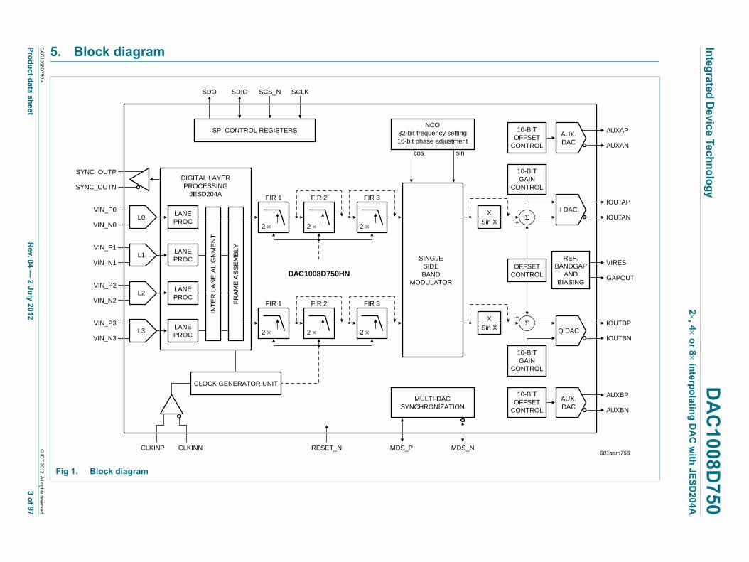
Fig 2. Pin configuration
001aam757
DAC1008D750HN
Transparent top view
AGND
VDDA(3V3)
AGND
VDDA(3V3)
AUXBP AUXAP
AUXBN AUXAN
AGND AGND
VDDA(1V8) VDDA(1V8)
VDDA(1V8) VDDA(1V8)
GAPOUT AGND
VIRES CLKINP
n.c. CLKINN
RESET_N AGND
SCS_N VDDA(1V8)
VDDD(1V8) MDS_P
SCLK MDS_N
SDIO VDDD(1V8)
SDO n.c.
VD
DA
(1V
8)
AG
ND
VD
DA
(1V
8)
VD
DA
(1V
8)
AG
ND
IOU
TB
N
IOU
TB
P
AG
ND
AG
ND
IOU
TA
P
IOU
TA
N
AG
ND
VD
DA
(1V
8)
VD
DA
(1V
8)
AG
ND
VD
DA
(1V
8)
JTA
G
n.c.
n.c.
VIN
_N3
VIN
_P3
VD
DD
(1V
8)
VIN
_P2
VIN
_N2
VIN
_N1
VIN
_P1
VD
DD
(1V
8)
VIN
_P0
VIN
_N0
SY
NC
_OU
TP
SY
NC
_OU
TN
VD
DD
(1V
8)
16 33
15 34
14 35
13 36
12 37
11 38
10 39
9 40
8 41
7 42
6 43
5 44
4 45
3 46
2 47
1 48
64 63 62 61 60 59 58 57 56 55 54 53 52 51 50 49
17 18 19 20 21 22 23 24 25 26 27 28 29 30 31 32
terminal 1index area
Table 2. Pin description
Symbol Pin Type[1] Description
SDO 1 O SPI data output
SDIO 2 I/O SPI data input/output
SCLK 3 I SPI clock
VDDD(1V8) 4 P digital supply voltage 1.8 V
SCS_N 5 I SPI chip select (active LOW)
RESET_N 6 I general reset (active LOW)
n.c. 7 - not connected
VIRES 8 I/O DAC biasing resistor
GAPOUT 9 I/O bandgap input/output voltage
VDDA(1V8) 10 P analog supply voltage 1.8 V
VDDA(1V8) 11 P analog supply voltage 1.8 V
DAC1008D750 4 © IDT 2012. All rights reserved.
Product data sheet Rev. 04 — 2 July 2012 4 of 97

Integrated Device Technology DAC1008D7502, 4 or 8 interpolating DAC with JESD204A
AGND 12 G analog ground
AUXBN 13 O complementary auxiliary DAC B output
AUXBP 14 O auxiliary DAC B output
VDDA(3V3) 15 P analog supply voltage 3.3 V
AGND 16 G analog ground
VDDA(1V8) 17 P analog supply voltage 1.8 V
AGND 18 G analog ground
VDDA(1V8) 19 P analog supply voltage 1.8 V
VDDA(1V8) 20 P analog supply voltage 1.8 V
AGND 21 G analog ground
IOUTBN 22 O complementary DAC B output current
IOUTBP 23 O DAC B output current
AGND 24 G analog ground
AGND 25 G analog ground
IOUTAP 26 O DAC A output current
IOUTAN 27 O complementary DAC A output current
AGND 28 G analog ground
VDDA(1V8) 29 P analog supply voltage 1.8 V
VDDA(1V8) 30 P analog supply voltage 1.8 V
AGND 31 G analog ground
VDDA(1V8) 32 P analog supply voltage 1.8 V
AGND 33 G analog ground
VDDA(3V3) 34 P analog supply voltage 3.3 V
AUXAP 35 O auxiliary DAC A output current
AUXAN 36 O complementary auxiliary DAC A output current
AGND 37 G analog ground
VDDA(1V8) 38 P analog supply voltage 1.8 V
VDDA(1V8) 39 P analog supply voltage 1.8 V
AGND 40 G analog ground
CLKINP 41 I clock input
CLKINN 42 I complementary clock input
AGND 43 G analog ground
VDDA(1V8) 44 P analog supply voltage 1.8 V
MDS_P 45 I/O multi-device synchronization
MDS_N 46 I/O complementary multi-device synchronization
VDDD(1V8) 47 P digital supply voltage 1.8 V
n.c. 48 - not connected
VDDD(1V8) 49 P digital supply voltage 1.8 V
SYNC_OUTN 50 O synchronization request to transmitter, complementary output
SYNC_OUTP 51 O synchronization request to transmitter
Table 2. Pin description …continued
Symbol Pin Type[1] Description
DAC1008D750 4 © IDT 2012. All rights reserved.
Product data sheet Rev. 04 — 2 July 2012 5 of 97

Integrated Device Technology DAC1008D7502, 4 or 8 interpolating DAC with JESD204A
[1] P: power supply; G: ground; I: input; O: output.
[2] H = heatsink (exposed die pad to be soldered to GND. A minimum of 81 thermal vias are required).
7. Limiting values
8. Thermal characteristics
[1] Complies with JEDEC test board, in free air.
VIN_N0 52 I serial interface lane 0 negative input
VIN_P0 53 I serial interface lane 0 positive input
VDDD(1V8) 54 P digital supply voltage 1.8 V
VIN_P1 55 I serial interface lane 1 positive input
VIN_N1 56 I serial interface lane 1 negative input
VIN_N2 57 I serial interface lane 2 negative input
VIN_P2 58 I serial interface lane 2 positive input
VDDD(1V8) 59 P digital supply voltage 1.8 V
VIN_P3 60 I serial interface lane 3 positive input
VIN_N3 61 I serial interface lane 3 negative input
n.c. 62 - not connected
n.c. 63 - not connected
JTAG 64 I JTAG test mode select (must be grounded)
GND H[2] G ground
Table 2. Pin description …continued
Symbol Pin Type[1] Description
Table 3. Limiting valuesIn accordance with the Absolute Maximum Rating System (IEC 60134).
Symbol Parameter Conditions Min Max Unit
VDDA(3V3) analog supply voltage (3.3 V) 0.5 +4.6 V
VDDA(1V8) analog supply voltage (1.8 V) 0.5 +2.5 V
VDDD digital supply voltage 0.5 +2.5 V
Tstg storage temperature 55 +150 C
Tamb ambient temperature 40 +85 C
Tj junction temperature 40 +125 C
Table 4. Thermal characteristics
Symbol Parameter Conditions Typ Unit
Rth(j-a) thermal resistance from junction to ambient [1] 18.7 K/W
Rth(j-c) thermal resistance from junction to case [1] 6.7 K/W
DAC1008D750 4 © IDT 2012. All rights reserved.
Product data sheet Rev. 04 — 2 July 2012 6 of 97
Integrated Device Technology DAC1008D7502, 4 or 8 interpolating DAC with JESD204A
9. Characteristics
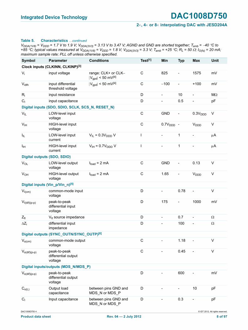
Table 5. CharacteristicsVDDA(1V8) = VDDD = 1.7 V to 1.9 V; VDDA(3V3) = 3.13 V to 3.47 V; AGND and GND are shorted together; Tamb = 40 C to +85 C; typical values measured at VDDA(1V8) = VDDD = 1.8 V; VDDA(3V3) = 3.3 V; Tamb = +25 C; RL = 50 ; IO(fs) = 20 mA; maximum sample rate; PLL off unless otherwise specified.
Symbol Parameter Conditions Test[1] Min Typ Max Unit
VDDA(3V3) analog supply voltage (3.3 V)
I 3.13 3.3 3.47 V
VDDD(1V8) digital supply voltage (1.8 V)
I 1.7 1.8 1.9 V
VDDA(1V8) analog supply voltage (1.8 V)
I 1.7 1.8 1.9 V
IDDA(3V3) analog supply current (3.3 V)
fo = 19 MHz; fs = 740 Msps; 4 interpolation; NCO on
I - 41 - mA
IDDD(1V8) digital supply current, (1.8 V)
fo = 19 MHz; fs = 740 Msps; 4 interpolation; NCO on
I - 356 - mA
IDDA(1V8) analog supply current, (1.8 V)
fo = 19 MHz; fs = 740 Msps; 4 interpolation; NCO on
I - 421 - mA
IDDD digital supply current difference
x/sin x function on; fs = 740 Msps
I - 54 - mA
Ptot total power dissipation fs = 740 Msps; interpolation; NCO off; DAC Q off
C - 0.80 - W
fs = 740 Msps; 4 interpolation; NCO off
C - 1.26 - W
fs = 740 Msps; 4 interpolation; NCO on
C - 1.50 - W
fs = 625 Msps; 2 interpolation; NCO off
C - 1.29 - W
fs = 625 Msps; 2 interpolation; NCO on
C - 1.46 - W
Power-down mode; fo = 19 MHz; fs = 740 Msps; 4 interpolation; NCO on
complete device; Power-down mode
I - 0.04 - W
DAC A and DAC B; Power-down mode
I - 0.60 - W
DAC A and DAC B; Sleep mode
I - 0.80 - W
Timing specifications
td(startup) start-up delay time from full Power-down mode - 20 - ms
td(restart) restart delay time from Sleep mode - 300 - ns
tlock lock time maximum input rate [2] - 11 - s
DAC1008D750 4 © IDT 2012. All rights reserved.
Product data sheet Rev. 04 — 2 July 2012 7 of 97
Integrated Device Technology DAC1008D7502, 4 or 8 interpolating DAC with JESD204A
Clock inputs (CLKINN, CLKINP)[3]
Vi input voltage range: CLK+ or CLK Vgpd < 50 mV[4]
C 825 - 1575 mV
Vidth input differential threshold voltage
Vgpd < 50 mV[4] C 100 - +100 mV
Ri input resistance D - 10 - M
CI input capacitance D - 0.5 - pF
Digital inputs (SDO, SDIO, SCLK, SCS_N, RESET_N)
VIL LOW-level input voltage
C GND - 0.3VDDD V
VIH HIGH-level input voltage
C 0.7VDDD - VDDD V
IIL LOW-level input current
VIL = 0.3VDDD V I - 1 - A
IIH HIGH-level input current
VIH = 0.7VDDD V I - 1 - A
Digital outputs (SDO, SDIO)
VOL LOW-level output voltage
Iload = 2 mA C GND - 0.13 V
VOH HIGH-level output voltage
Iload = 2 mA C 1.65 - VDDD V
Digital inputs (Vin_p/Vin_n)[5]
VI(cm) common-mode input voltage
D - 0.78 - V
VI(dif)(p-p) peak-to-peak differential input voltage
D 175 - 1000 mV
Ztt Vtt source impedance D - 0.7 -
Zi differential input impedance
D - 100 -
Digital outputs (SYNC_OUTN/SYNC_OUTP)[6]
Vo(cm) common-mode output voltage
C - 1.18 - V
Vo(dif)(p-p) peak-to-peak differential output voltage
C - 0.45 - V
Digital inputs/outputs (MDS_N/MDS_P)
Vo(dif)(p-p) peak-to-peak differential output voltage
D - 600 - mV
Co(L) Output load capacitance
between pins GND and MDS_N or MDS_P
D - - 10 pF
CI Input capacitance between pins GND and MDS_N or MDS_P
D - 0.3 - pF
Table 5. Characteristics …continuedVDDA(1V8) = VDDD = 1.7 V to 1.9 V; VDDA(3V3) = 3.13 V to 3.47 V; AGND and GND are shorted together; Tamb = 40 C to +85 C; typical values measured at VDDA(1V8) = VDDD = 1.8 V; VDDA(3V3) = 3.3 V; Tamb = +25 C; RL = 50 ; IO(fs) = 20 mA; maximum sample rate; PLL off unless otherwise specified.
Symbol Parameter Conditions Test[1] Min Typ Max Unit
DAC1008D750 4 © IDT 2012. All rights reserved.
Product data sheet Rev. 04 — 2 July 2012 8 of 97
Integrated Device Technology DAC1008D7502, 4 or 8 interpolating DAC with JESD204A
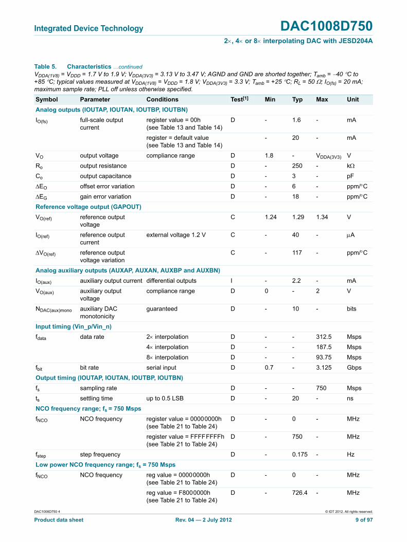
Analog outputs (IOUTAP, IOUTAN, IOUTBP, IOUTBN)
IO(fs) full-scale output current
register value = 00h (see Table 13 and Table 14)
D - 1.6 - mA
register = default value (see Table 13 and Table 14)
- 20 - mA
VO output voltage compliance range D 1.8 - VDDA(3V3) V
Ro output resistance D - 250 - k
Co output capacitance D - 3 - pF
EO offset error variation D - 6 - ppm/C
EG gain error variation D - 18 - ppm/C
Reference voltage output (GAPOUT)
VO(ref) reference output voltage
C 1.24 1.29 1.34 V
IO(ref) reference output current
external voltage 1.2 V C - 40 - A
VO(ref) reference output voltage variation
C - 117 - ppm/C
Analog auxiliary outputs (AUXAP, AUXAN, AUXBP and AUXBN)
IO(aux) auxiliary output current differential outputs I - 2.2 - mA
VO(aux) auxiliary output voltage
compliance range D 0 - 2 V
NDAC(aux)mono auxiliary DAC monotonicity
guaranteed D - 10 - bits
Input timing (Vin_p/Vin_n)
fdata data rate 2 interpolation D - - 312.5 Msps
4 interpolation D - - 187.5 Msps
8 interpolation D - - 93.75 Msps
fbit bit rate serial input D 0.7 - 3.125 Gbps
Output timing (IOUTAP, IOUTAN, IOUTBP, IOUTBN)
fs sampling rate D - - 750 Msps
ts settling time up to 0.5 LSB D - 20 - ns
NCO frequency range; fs = 750 Msps
fNCO NCO frequency register value = 00000000h (see Table 21 to Table 24)
D - 0 - MHz
register value = FFFFFFFFh (see Table 21 to Table 24)
D - 750 - MHz
fstep step frequency D - 0.175 - Hz
Low power NCO frequency range; fs = 750 Msps
fNCO NCO frequency reg value = 00000000h (see Table 21 to Table 24)
D - 0 - MHz
reg value = F8000000h (see Table 21 to Table 24)
D - 726.4 - MHz
Table 5. Characteristics …continuedVDDA(1V8) = VDDD = 1.7 V to 1.9 V; VDDA(3V3) = 3.13 V to 3.47 V; AGND and GND are shorted together; Tamb = 40 C to +85 C; typical values measured at VDDA(1V8) = VDDD = 1.8 V; VDDA(3V3) = 3.3 V; Tamb = +25 C; RL = 50 ; IO(fs) = 20 mA; maximum sample rate; PLL off unless otherwise specified.
Symbol Parameter Conditions Test[1] Min Typ Max Unit
DAC1008D750 4 © IDT 2012. All rights reserved.
Product data sheet Rev. 04 — 2 July 2012 9 of 97
Integrated Device Technology DAC1008D7502, 4 or 8 interpolating DAC with JESD204A
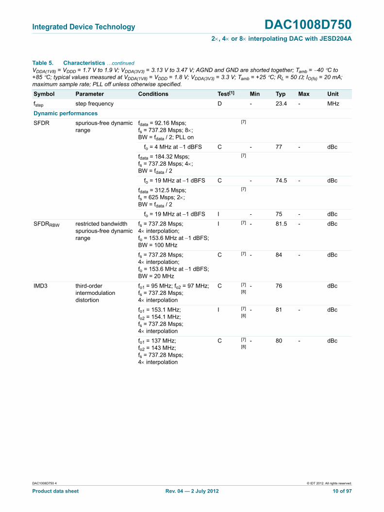
fstep step frequency D - 23.4 - MHz
Dynamic performances
SFDR spurious-free dynamic range
fdata = 92.16 Msps; fs = 737.28 Msps; 8; BW = fdata / 2; PLL on
[7]
fo = 4 MHz at 1 dBFS C - 77 - dBc
fdata = 184.32 Msps; fs = 737.28 Msps; 4; BW = fdata / 2
[7]
fo = 19 MHz at 1 dBFS C - 74.5 - dBc
fdata = 312.5 Msps; fs = 625 Msps; 2; BW = fdata / 2
[7]
fo = 19 MHz at 1 dBFS I - 75 - dBc
SFDRRBW restricted bandwidth spurious-free dynamic range
fs = 737.28 Msps; 4 interpolation; fo = 153.6 MHz at 1 dBFS; BW = 100 MHz
I [7] - 81.5 - dBc
fs = 737.28 Msps; 4 interpolation; fo = 153.6 MHz at 1 dBFS; BW = 20 MHz
C [7] - 84 - dBc
IMD3 third-order intermodulation distortion
fo1 = 95 MHz; fo2 = 97 MHz; fs = 737.28 Msps; 4 interpolation
C [7]
[8]- 76 dBc
fo1 = 153.1 MHz; fo2 = 154.1 MHz; fs = 737.28 Msps; 4 interpolation
I [7]
[8]- 81 - dBc
fo1 = 137 MHz; fo2 = 143 MHz; fs = 737.28 Msps; 4 interpolation
C [7]
[8]- 80 - dBc
Table 5. Characteristics …continuedVDDA(1V8) = VDDD = 1.7 V to 1.9 V; VDDA(3V3) = 3.13 V to 3.47 V; AGND and GND are shorted together; Tamb = 40 C to +85 C; typical values measured at VDDA(1V8) = VDDD = 1.8 V; VDDA(3V3) = 3.3 V; Tamb = +25 C; RL = 50 ; IO(fs) = 20 mA; maximum sample rate; PLL off unless otherwise specified.
Symbol Parameter Conditions Test[1] Min Typ Max Unit
DAC1008D750 4 © IDT 2012. All rights reserved.
Product data sheet Rev. 04 — 2 July 2012 10 of 97

Integrated Device Technology DAC1008D7502, 4 or 8 interpolating DAC with JESD204A
[1] D = guaranteed by design; C = guaranteed by characterization; I = 100 % industrially tested.
[2] Delay between the deassertion of bits FORCE_RESET_FCLK and FORCE_RESET_DCLK and the deassertion of the sync signal. It reflects the delay required by DAC1008D750 to lock to a JESD204A stream. It supposes that the TX is already transmitting K28.5 characters in error-free conditions.
[3] CLKINP/CLKINN inputs are at differential LVDS levels. An external termination resistor with a value of between 80 and 120 (see Figure 15) should be connected across the pins.
[4] Vgpd represents the ground potential difference voltage. This is the voltage that results from current flowing through the finite resistance and the inductance between the receiver and the driver circuit ground voltage.
[5] Vin_p and Vin_n inputs are differential CML inputs. They are terminated internally to Vtt via 50 (see Figure 4).
[6] SYNC_OUTP/SYNC_OUTN outputs are differential LVDS outputs. They must be terminated by a resistor with a value of between 80 and 120 .
[7] Optimum performances at high sampling rate (> 650 Msps) will be achieved with VDDA(1V8) = 1.8 V 2 %
[8] IMD3 rejection with 6 dBFS/tone.
ACPR adjacent channel power ratio
NCO on; interpolation; fs = 737.28 Msps; fo = 96 MHz
[7]
1 carrier; BW = 5 MHz C - 67 - dBc
2 carriers; BW = 10 MHz C - 64 - dBc
4 carriers; BW = 20 MHz C - 60 - dBc
NCO on; 4 interpolation; fs = 737.28 Msps; fo = 153.6 MHz
[7]
1 carrier; BW = 5 MHz C - 67 - dBc
2 carriers; BW = 10 MHz C - 64 - dBc
4 carriers; BW = 20 MHz C - 59 - dBc
NSD noise spectral density fs = 737.28 Msps; 4 interpolation; fo = 153.6 MHz at 0 dBFS
I [7] - 145 - dBm/Hz
Table 5. Characteristics …continuedVDDA(1V8) = VDDD = 1.7 V to 1.9 V; VDDA(3V3) = 3.13 V to 3.47 V; AGND and GND are shorted together; Tamb = 40 C to +85 C; typical values measured at VDDA(1V8) = VDDD = 1.8 V; VDDA(3V3) = 3.3 V; Tamb = +25 C; RL = 50 ; IO(fs) = 20 mA; maximum sample rate; PLL off unless otherwise specified.
Symbol Parameter Conditions Test[1] Min Typ Max Unit
DAC1008D750 4 © IDT 2012. All rights reserved.
Product data sheet Rev. 04 — 2 July 2012 11 of 97

Integrated Device Technology DAC1008D7502, 4 or 8 interpolating DAC with JESD204A
10. Application information
10.1 General description
The DAC1008D750 is a dual 10-bit DAC operating up to 750 Msps. With a maximum input data rate of up to 312.5 Msps and a maximum output sampling rate of 750 Msps, the DAC1008D750 allows more flexibility for wide bandwidth and multi-carrier systems. Combined with its quadrature modulator and 32-bit NCO, the DAC1008D750 simplifies the frequency selection of the system. This is also possible because of the 2, 4 or 8 interpolation filters which remove undesired images.
DAC1008D750 supports the following JESD204A key features:
• 10-bit/8-bit decoding
• Code group synchronization
• inter-lane alignment
• 1 + x14 + x15 scrambling polynomial
• Character replacement
• TX/RX synchronization management via SYNC signals
• Multiple Converter Device Alignment-Multiple Lanes (MCDA-ML) device
DAC1008D750 can be interfaced with any logic device that features high-speed SERDES functionality. This macro is now widely available in FPGA from different vendors. Standalone SERDES ICs can also be used.
To enhance the intrinsic board layout simplification of the JESD204A standard, IDT includes polarity swapping for each of the lanes and additionally offers lane swapping. Each physical lane can be configured logically as lane0, lane1, lane2 or lane3.
This device is MCDA-ML compliant, offering inter-lane alignment between several devices. Samples alignment between devices is maintained up to output level because of an IDT proprietary mechanism. One device is configured as the master and all the others are configured as slaves. These will automatically align their output samples to the master ones. Therefore, a system with several DAC1008D750s can produce data with a guaranteed alignment of less than 1 DAC output clock period.
Each DAC generates two complementary current outputs on pins IOUTAP/IOUTAN and IOUTBP/IOUTBN. This provides a full-scale output current of up to 20 mA. An internal reference is available for the reference current which is externally adjustable using pin VIRES.
The DAC1008D750 must be configured before operating. Therefore, it features an SPI slave interface to access internal registers. Some of these registers also provide information about the JESD204A interface status.
The DAC1008D750 requires supplies of both 3.3 V and 1.8 V. The 1.8 V supply has separate digital and analog power supply pins. The clock input is LVDS compliant.
DAC1008D750 4 © IDT 2012. All rights reserved.
Product data sheet Rev. 04 — 2 July 2012 12 of 97

Integrated Device Technology DAC1008D7502, 4 or 8 interpolating DAC with JESD204A
10.2 JESD204A receiver
The JEDEC204A defines the following parameters:
L is the number of lanes per link
M is the number of converters per device
F is the number of bytes per frame clock period
The DAC1008D750 supports both LMF = 421 and LMF = 211. The current setting is configurable via the SPI registers interface.
The complete Digital Layer Processing (DLP) adds a variable delay on each lane path. This is mainly because of the inter-lane alignment.
[1] D = guaranteed by design.
[2] Frame clock cycle.
The descrambler can be enabled/disabled
Fig 3. JESD204A receiver
10b10b
005aaa157
SYNC_OUTinternal
configurationinterface
DES CLOCKALIGN
frameclock
lane#10b 10b
10b
SYNCAND
WORDALIGN
8bK-DETECT10b/8b
8b8b
8b
8b
8b
DESCRAMBLER
RX CONTROLLER
ILA
(Int
er-la
ne A
lignm
ent)
FA
(Fra
me
Ass
embl
y)
Table 6. Digital Layer Processing Latency
Symbol Parameter Conditions Test[1] Min Typ Max Unit
td delay time digital layer processing delay
D 13 - 28 cycle[2]
DAC1008D750 4 © IDT 2012. All rights reserved.
Product data sheet Rev. 04 — 2 July 2012 13 of 97

Integrated Device Technology DAC1008D7502, 4 or 8 interpolating DAC with JESD204A
10.2.1 Lane input
Each lane is CML compliant. It is terminated to a common voltage with an integrated 50 resistor.
The common-mode voltage is programmable by the SET_VCM_VOLTAGE register as shown in Table 75 on page 56.
DC coupling is only possible if both the DAC and the transmitter have the same common-mode voltage. If this is not the case, AC coupling is required.
The deserializer performs the incoming data clock recovery and also the serial-to-parallel conversion. Therefore, each lane includes its own PLL that must first lock.
The clock alignment module transfers the data from the regenerated clock to the frame clock domain. The frequency of both clocks is the same but the phase relationship between the clocks is unknown.
10.2.2 Sync and word align
As stated in JESD204A, the transmitter and the receiver first have to synchronize. This is achieved through the SYNC_OUT signals and a sync pattern (K28.5 symbol). The receiver (i.e. DAC1008D750) first drives its SYNC_OUT outputs. The sync pattern is continuously sent until the receiver deasserts the SYNC_OUT signal.
Fig 4. Lane input termination
Vtt
001aak166
50 Ω
Ztt
50 Ω
Vin_p
Vin_n
Fig 5. DC coupling Fig 6. AC coupling
001aak162
50 Ω 50 Ω 50 Ω 50 Ω
Zdiff = 100 Ω
data in +
data in −
001aak163
50 Ω 50 Ω 50 Ω 50 Ω
Zdiff = 100 Ω
VDD1 VDD2
data in +
data in −
DAC1008D750 4 © IDT 2012. All rights reserved.
Product data sheet Rev. 04 — 2 July 2012 14 of 97

Integrated Device Technology DAC1008D7502, 4 or 8 interpolating DAC with JESD204A
The lane processing makes use of the sync patterns to synchronize the datastream, determine the initial running disparity and extract the 10-bit word from the incoming datastream (word-alignment).
The SYNC_OUT signal is also used during normal operation by the DAC1008D750 to request a link reinitialization. This occurs when the 10b/8b module loses synchronization.
The SYNC_OUT signal conforms to LVDS signaling. Its common-mode voltage and its single-ended peak amplitude can be programmed using SET_SYNC_LEVEL bits in the SET_SYNC registers (see Table 77 on page 56).
SYNC_OUT is asynchronous with the frame clock. There is no timing specification with respect to the CLKINP and CLKINN inputs.
10.2.3 Comma detection and word align
This stage monitors the datastream for code characters (Comma detection), decodes the words to bytes (octets) and performs optional character replacement as part of frame/lane alignment monitoring and correction. This module provides the required control signals to the RX-controller and ILA.
This module decodes the 10-bit words into 8-bit words (octets). The decoding table is specified in the IEEE 802.3-2005 specification. During decoding, the disparity is calculated according to the disparity rules mentioned in the same specification IEEE 802.3-2005. When the disparity counter is more than +2 or less than 2, an error will be generated.
The following comma symbols are detected during data transmission irrespective of the running disparity:
/K/ = K28.5
/F/ = K28.7
/A/ = K28.3
/R/ = K28.0
/Q/ = K28.4
A flag is sent to the control interface to reflect detected commas in registers.
The following flags are also triggered according to the following definitions:
• VALID: a code group that is found in the column of the 10b/8b decoding tables according to the current running disparity.
• DISPARITY ERROR: The received code group exists in the 10b/8b decoding table, but is not found in the proper column according to the current running disparity.
• NOT-IN-TABLE (NIT) ERROR: The received code group is not found in the 10b/8b decoding table for either disparity.
• INVALID: a code group that either shows a disparity error or that does not exist in the 10b/8b decoding table.
DAC1008D750 supports character replacement whatever the state of the descrambler. When scrambling is not active, the received K28.3 /A/ or K28.7 /F/ will be replaced by the previous sample. When scrambling is active, the corresponding data octet D28.3 (0xC) or D28.7 (0xFC) will be used.
DAC1008D750 4 © IDT 2012. All rights reserved.
Product data sheet Rev. 04 — 2 July 2012 15 of 97
Integrated Device Technology DAC1008D7502, 4 or 8 interpolating DAC with JESD204A
10.2.4 Descrambler
The descrambler is a 16-bit parallel self-synchronous descrambler based on the polynomial 1 + x14 + x15. This processing can be turned off.
10.2.5 Inter-lane alignment
This feature removes strict PCB design skew compensation between the lanes.
10.2.5.1 Single device operation
This module handles the alignment of the four data streams. Because of inter-lane skew and each PLL per lane concept, these alignment characters may be received at different times by the receivers. After the synchronization period, the lock signal will be HIGH. This enables the receipt of K28.3 /A/ characters.
The ILA_CNTRL register’s SEL_ILA[1:0] bits select which K28.3 /A/ symbol triggers the initial lane alignment:“00” = 1st /A/ symbol, “01” = 2nd /A/ symbol, “10” = 3rd /A/ symbol, “11” = 4th /A/ symbol; Table 86 on page 62. When all receivers have received their first selected /A/, they start propagating the received data to the frame assembly module at the same point in time.
This module can compensate for up to 7 frame clock period misalignments between the lanes.
When initial lane alignment is not supported, the manual alignment mode can be used.
After the initial ILA sequence, the lane alignment monitoring starts. If the received user data contains K28.3 /A/ symbol:
• its position is compared to the value of the alignment monitor counter
• if two successive K28.3 /A/ symbols have been received at a wrong position, a realignment takes place
• if the buffers are empty or overflow, this is indicated by the registers ILA_BUF_ERR_LN0 to ILA_BUF_ERR_LN3
10.2.5.2 Multi-device operation
DAC1008D750 implements a multi-device inter-lane alignment that guarantees a skew of less than one output period between them.
Two modes are available: master/slave and all slave. Both make use of the MDS_P and MDS_N pins.
DAC1008D750 4 © IDT 2012. All rights reserved.
Product data sheet Rev. 04 — 2 July 2012 16 of 97
Integrated Device Technology DAC1008D7502, 4 or 8 interpolating DAC with JESD204A
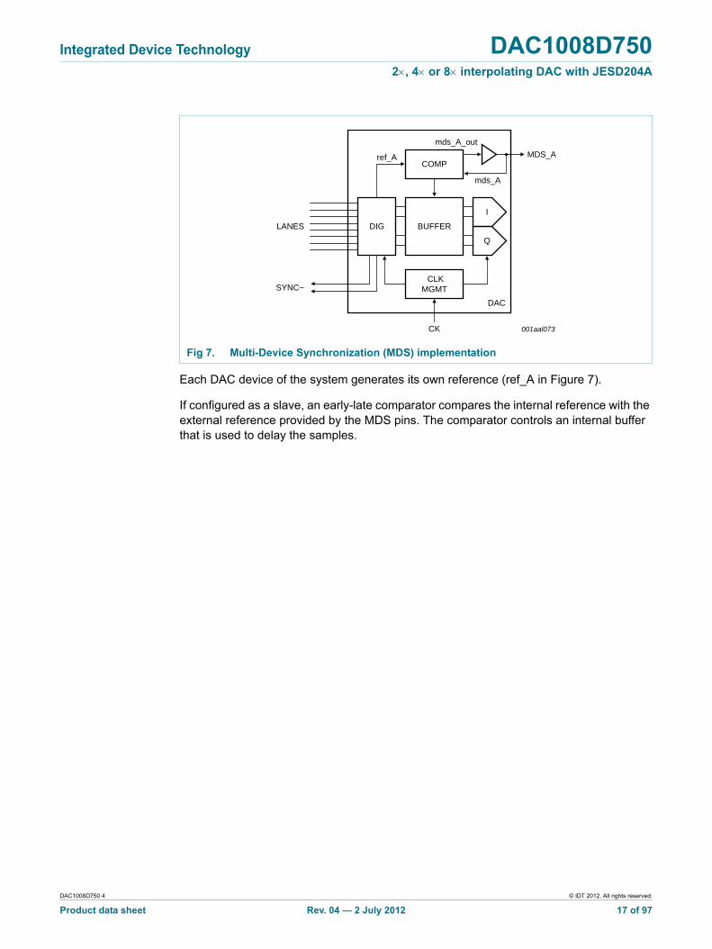
Each DAC device of the system generates its own reference (ref_A in Figure 7).
If configured as a slave, an early-late comparator compares the internal reference with the external reference provided by the MDS pins. The comparator controls an internal buffer that is used to delay the samples.
Fig 7. Multi-Device Synchronization (MDS) implementation
001aal073
I
BUFFER
Q
DIGLANES
COMPMDS_Aref_A
SYNC~
mds_A_out
mds_A
CK
DAC
CLKMGMT
DAC1008D750 4 © IDT 2012. All rights reserved.
Product data sheet Rev. 04 — 2 July 2012 17 of 97
Integrated Device Technology DAC1008D7502, 4 or 8 interpolating DAC with JESD204A
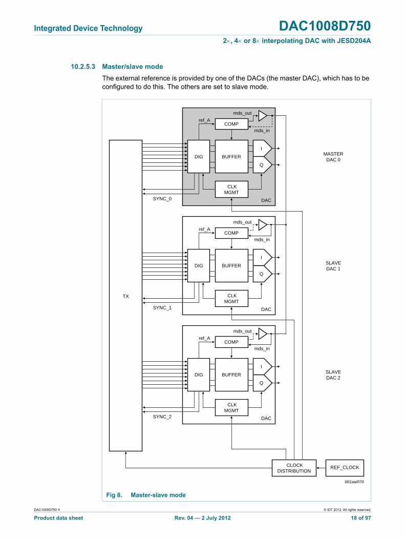
10.2.5.3 Master/slave mode
The external reference is provided by one of the DACs (the master DAC), which has to be configured to do this. The others are set to slave mode.
Fig 8. Master-slave mode
001aal070
ref_A
SYNC_0
mds_out
mds_in
I
BUFFER
Q
DIG
COMPref_A
SYNC_1
mds_out
mds_in
DAC
CLKMGMT
I
BUFFER
MASTERDAC 0
SLAVEDAC 1
SLAVEDAC 2
Q
DIG
TX
COMPref_A
SYNC_2
mds_out
mds_in
DAC
CLKMGMT
CLOCKDISTRIBUTION
REF_CLOCK
Q
I
BUFFERDIG
COMP
DAC
CLKMGMT
DAC1008D750 4 © IDT 2012. All rights reserved.
Product data sheet Rev. 04 — 2 July 2012 18 of 97

Integrated Device Technology DAC1008D7502, 4 or 8 interpolating DAC with JESD204A
The MDS signal generated by the master DAC must reach all slaves within one DAC output clock period. This induces PCB layout constraints for the MDS signal and also for the clock distribution. Because trace lengths differ, the clock edges will reach each of the DACs at different times.
The worst case clock skew is given by t1 = PH01 PH03, where PH0x represents the sum of the trace delay and the clock skew at the output of the clock generator.
The maximum allowable trace delay for the MDS signal is given by t = TDAC t1.
Fig 9. Clock skew case 1: Master is the farthest
001aal072
ref clock
TDAC
master clock
PH03
slave 1 clock
PH02
slave 2 clock
PH01
DAC1008D750 4 © IDT 2012. All rights reserved.
Product data sheet Rev. 04 — 2 July 2012 19 of 97
Integrated Device Technology DAC1008D7502, 4 or 8 interpolating DAC with JESD204A
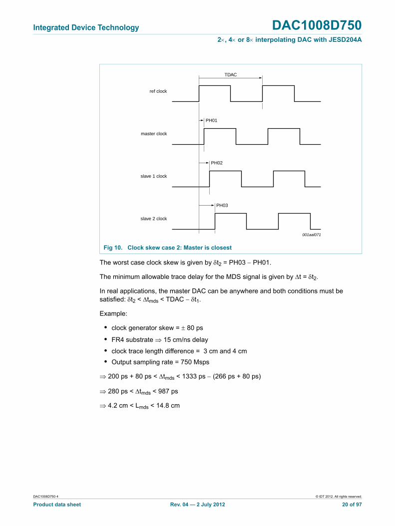
The worst case clock skew is given by t2 = PH03 PH01.
The minimum allowable trace delay for the MDS signal is given by t = t2.
In real applications, the master DAC can be anywhere and both conditions must be satisfied: t2 < tmds < TDAC t1.
Example:
• clock generator skew = 80 ps
• FR4 substrate 15 cm/ns delay
• clock trace length difference = 3 cm and 4 cm
• Output sampling rate = 750 Msps
200 ps + 80 ps < tmds < 1333 ps (266 ps + 80 ps)
280 ps < tmds < 987 ps
4.2 cm < Lmds < 14.8 cm
Fig 10. Clock skew case 2: Master is closest
001aal071
ref clock
TDAC
master clock
PH01
slave 1 clock
PH02
slave 2 clock
PH03
DAC1008D750 4 © IDT 2012. All rights reserved.
Product data sheet Rev. 04 — 2 July 2012 20 of 97
Integrated Device Technology DAC1008D7502, 4 or 8 interpolating DAC with JESD204A
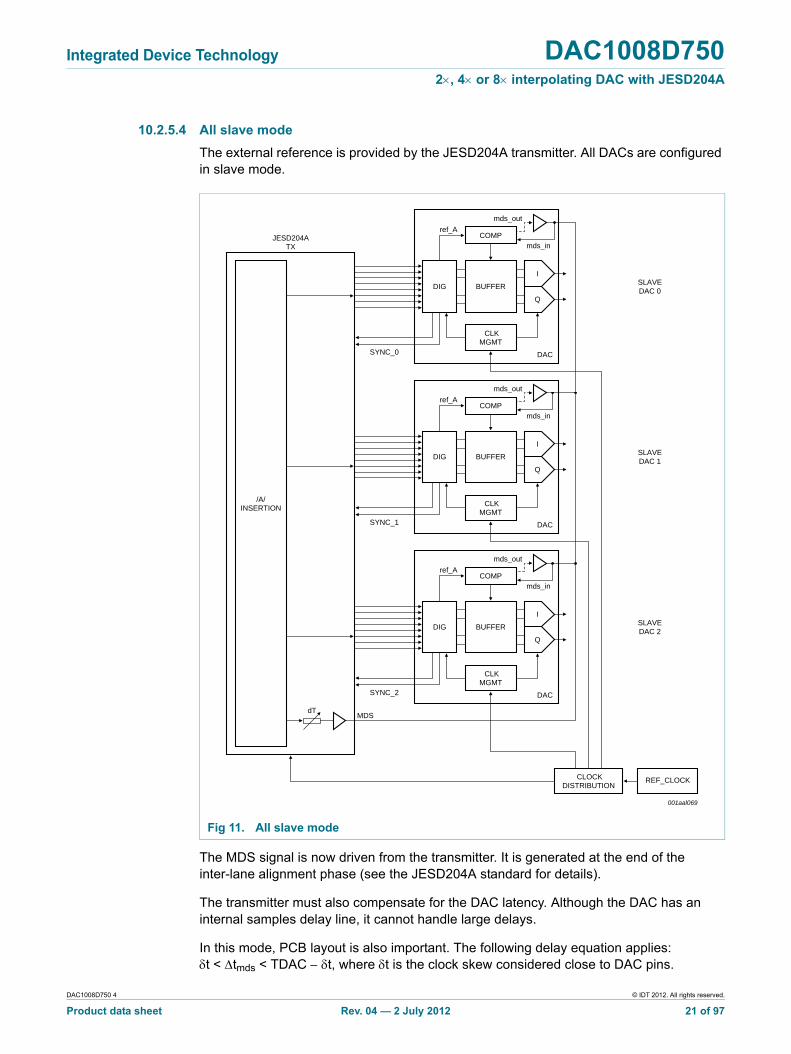
10.2.5.4 All slave mode
The external reference is provided by the JESD204A transmitter. All DACs are configured in slave mode.
The MDS signal is now driven from the transmitter. It is generated at the end of the inter-lane alignment phase (see the JESD204A standard for details).
The transmitter must also compensate for the DAC latency. Although the DAC has an internal samples delay line, it cannot handle large delays.
In this mode, PCB layout is also important. The following delay equation applies: t < tmds < TDAC t, where t is the clock skew considered close to DAC pins.
Fig 11. All slave mode
001aal069
I
BUFFER
Q
DIG
COMPref_A
SYNC_0
JESD204ATX
mds_out
mds_in
DAC
CLKMGMT
I
BUFFER
Q
DIG
COMPref_A
SYNC_1
mds_out
mds_in
DAC
CLKMGMT
I
BUFFER
SLAVEDAC 0
SLAVEDAC 1
SLAVEDAC 2
Q
DIG
/A/INSERTION
COMPref_A
SYNC_2
MDSdT
mds_out
mds_in
DAC
CLKMGMT
CLOCKDISTRIBUTION
REF_CLOCK
DAC1008D750 4 © IDT 2012. All rights reserved.
Product data sheet Rev. 04 — 2 July 2012 21 of 97
Integrated Device Technology DAC1008D7502, 4 or 8 interpolating DAC with JESD204A
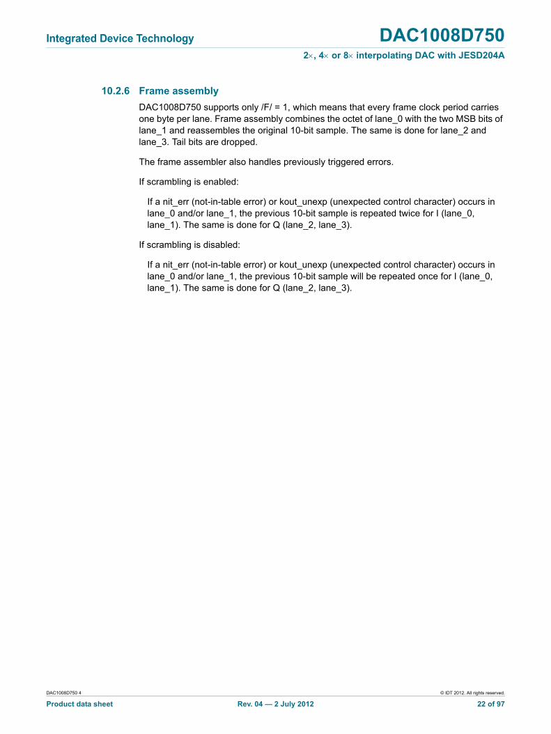
10.2.6 Frame assembly
DAC1008D750 supports only /F/ = 1, which means that every frame clock period carries one byte per lane. Frame assembly combines the octet of lane_0 with the two MSB bits of lane_1 and reassembles the original 10-bit sample. The same is done for lane_2 and lane_3. Tail bits are dropped.
The frame assembler also handles previously triggered errors.
If scrambling is enabled:
If a nit_err (not-in-table error) or kout_unexp (unexpected control character) occurs in lane_0 and/or lane_1, the previous 10-bit sample is repeated twice for I (lane_0, lane_1). The same is done for Q (lane_2, lane_3).
If scrambling is disabled:
If a nit_err (not-in-table error) or kout_unexp (unexpected control character) occurs in lane_0 and/or lane_1, the previous 10-bit sample will be repeated once for I (lane_0, lane_1). The same is done for Q (lane_2, lane_3).
DAC1008D750 4 © IDT 2012. All rights reserved.
Product data sheet Rev. 04 — 2 July 2012 22 of 97
Integrated Device Technology DAC1008D7502, 4 or 8 interpolating DAC with JESD204A
Fig 12. Frame assembly
005aaa153
DAC0
SERIAL CLOCK3.125 GHz
encodedoctet
b9
b0
lane 0
b1b2b3b4b5b6b7b8b9
DE
SE
RIA
LIZ
ER
b8
b7
b6
b5
b4
b3
b2
b1
b0
CHARACTER CLOCK312.5 MHz
scrambledoctet
S7
10b/
8b
S6
S5
S4
S3
S2
S1
S0
FRAME CLOCK312.5 MHz
byte 0
/F
D09
ON/OFF/10
DE
SC
RA
MB
LER
D08
D07
D06
D05
D04
D03
D02
encodedoctet
b9
b0
lane 1
b1b2b3b4b5b6b7b8b9
DE
SE
RIA
LIZ
ER
b8
b7
b6
b5
b4
b3
b2
b1
b0
scrambledoctet
S7
10b/
8b
S6
S5
S4
S3
S2
S1
S0
byte 1
D01
ON/OFF/10
DE
SC
RA
MB
LER
FR
AM
E A
SS
EM
BLY
D00
T
T
T
T
T
T
byte 2
F = 1 byte M = 2 converters
D09
D08
D07
D06
D05
D04
D03
D02
D09
D08
D07
D06
D05
D04
D03
D02
D01
D00
D09
D08
D07
D06
D05
D04
D03
D02
D01
D00
byte 3
D01
D00
T
T
T
T
T
T
encodedoctet
b9
b0
lane 2
b1b2b3b4b5b6b7b8b9
DE
SE
RIA
LIZ
ER
b8
b7
b6
b5
b4
b3
b2
b1
b0
scrambledoctet
S7
10b/
8b
S6
S5
S4
S3
S2
S1
S0
ON/OFF/10
DE
SC
RA
MB
LER
encodedoctet
b9
b0
lane 3
b1b2b3b4b5b6b7b8b9
DE
SE
RIA
LIZ
ER
b8
b7
b6
b5
b4
b3
b2
b1
b0
scrambledoctet
S7
10b/
8b
S6
S5
S4
S3
S2
S1
S0
ON/OFF/10
DE
SC
RA
MB
LER
DAC1
DAC1008D750 4 © IDT 2012. All rights reserved.
Product data sheet Rev. 04 — 2 July 2012 23 of 97
Integrated Device Technology DAC1008D7502, 4 or 8 interpolating DAC with JESD204A
10.3 Serial Peripheral Interface (SPI)
10.3.1 Protocol description
The DAC1008D750 serial interface is a synchronous serial communication port allowing easy interfacing with many industry microprocessors. It provides access to the registers that define the operating modes of the chip in both Write mode and Read mode.
This interface can be configured as a 3-wire type (SDIO as bidirectional pin) or a 4-wire type (SDIO and SDO as unidirectional pin, input and output port respectively). In both configurations, SCLK acts as the serial clock and SCS_N acts as the serial chip select bar.
Each read/write operation is sequenced by the SCS_N signal and enabled by a LOW assertion to drive the chip with two bytes to five bytes, depending on the content of the instruction byte (see Table 8).
In Table 8 below, N1 and N0 indicate the number of bytes transferred after the instruction byte.
A[4:0] indicates which register is being addressed. In the case of a multiple transfer, this address points to the first register to be accessed. The address is then internally decreased after each following data phase.
R/W indicates the mode access (see Table 7).
Fig 13. SPI protocol
001aaj812
RESET_N
SCS_N
SCLK
SDIO
SDO(optional)
R/W N1 N0 A4 A3 A2 A1 A0 D7 D6 D5 D4 D3 D2 D1 D0
D7 D6 D5 D4 D3 D2 D1 D0
Table 7. Read or Write mode access description
R/W Description
0 Write mode operation
1 Read mode operation
Table 8. Number of bytes to be transferred
N1 N0 Number of bytes transferred
0 0 1
0 1 2
1 0 3
1 1 4
DAC1008D750 4 © IDT 2012. All rights reserved.
Product data sheet Rev. 04 — 2 July 2012 24 of 97
Integrated Device Technology DAC1008D7502, 4 or 8 interpolating DAC with JESD204A
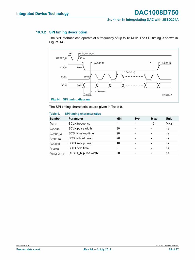
10.3.2 SPI timing description
The SPI interface can operate at a frequency of up to 15 MHz. The SPI timing is shown in Figure 14.
The SPI timing characteristics are given in Table 9.
Fig 14. SPI timing diagram
Table 9. SPI timing characteristics
Symbol Parameter Min Typ Max Unit
fSCLK SCLK frequency - - 15 MHz
tw(SCLK) SCLK pulse width 30 - - ns
tsu(SCS_N) SCS_N set-up time 20 - - ns
th(SCS_N) SCS_N hold time 20 - - ns
tsu(SDIO) SDIO set-up time 10 - - ns
th(SDIO) SDIO hold time 5 - - ns
tw(RESET_N) RESET_N pulse width 30 - - ns
001aaj813
50 %
tw(RESET_N)
tsu(SCS_N)
tsu(SDIO)
th(SDIO)
th(SCS_N)
tw(SCLK)
50 %
RESET_N
SCS_N
SCLK
SDIO
50 %
50 %
DAC1008D750 4 © IDT 2012. All rights reserved.
Product data sheet Rev. 04 — 2 July 2012 25 of 97
Integrated Device Technology DAC1008D7502, 4 or 8 interpolating DAC with JESD204A
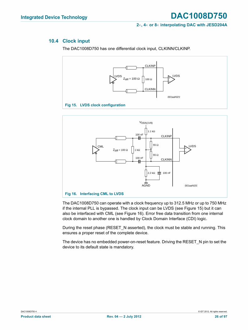
10.4 Clock input
The DAC1008D750 has one differential clock input, CLKINN/CLKINP.
The DAC1008D750 can operate with a clock frequency up to 312.5 MHz or up to 750 MHz if the internal PLL is bypassed. The clock input can be LVDS (see Figure 15) but it can also be interfaced with CML (see Figure 16). Error free data transition from one internal clock domain to another one is handled by Clock Domain Interface (CDI) logic.
During the reset phase (RESET_N asserted), the clock must be stable and running. This ensures a proper reset of the complete device.
The device has no embedded power-on-reset feature. Driving the RESET_N pin to set the device to its default state is mandatory.
Fig 15. LVDS clock configuration
Fig 16. Interfacing CML to LVDS
001aah021
100 ΩLVDS
CLKINP
CLKINN
LVDSZdiff = 100 Ω
001aah020
55 Ω
55 Ω
1.1 kΩ
2.2 kΩ
100 nF
CML
100 nF
100 nF
CLKINP
LVDS
CLKINN
AGND
VDDA(1V8)
1 kΩZdiff = 100 Ω
DAC1008D750 4 © IDT 2012. All rights reserved.
Product data sheet Rev. 04 — 2 July 2012 26 of 97

Integrated Device Technology DAC1008D7502, 4 or 8 interpolating DAC with JESD204A
10.5 FIR filters
The three interpolation FIR filters have a stop band attenuation of at least 80 dBc and a pass band ripple of less than 0.0005 dB.
Table 10. Interpolation filter coefficients
First interpolation filter Second interpolation filter Third interpolation filter
Lower Upper Value Lower Upper Value Lower Upper Value
H(1) H(55) 4 H(1) H(23) 2 H(1) H(15) 39
H(2) H(54) 0 H(2) H(22) 0 H(2) H(14) 0
H(3) H(53) 13 H(3) H(21) 17 H(3) H(13) 273
H(4) H(52) 0 H(4) H(20) 0 H(4) H(12) 0
H(5) H(51) 34 H(5) H(19) 75 H(5) H(11) 1102
H(6) H(50) 0 H(6) H(18) 0 H(6) H(10) 0
H(7) H(49) 72 H(7) H(17) 238 H(7) H(9) 4964
H(8) H(48) 0 H(8) H(16) 0 H(8) - 8192
H(9) H(47) 138 H(9) H(15) 660 - - -
H(10) H(46) 0 H(10) H(14) 0 - - -
H(11) H(45) 245 H(11) H(13) 2530 - - -
H(12) H(44) 0 H(12) - 4096 - - -
H(13) H(43) 408 - - - - - -
H(14) H(42) 0 - - - - - -
H(15) H(41) 650 - - - - - -
H(16) H(40) 0 - - - - - -
H(17) H(39) 1003 - - - - - -
H(18) H(38) 0 - - - - - -
H(19) H(37) 1521 - - - - - -
H(20) H(36) 0 - - - - - -
H(21) H(35) 2315 - - - - - -
H(22) H(34) 0 - - - - - -
H(23) H(33) 3671 - - - - - -
H(24) H(32) 0 - - - - - -
H(25) H(31) 6642 - - - - - -
H(26) H(30) 0 - - - - - -
H(27) H(29) 20756 - - - - - -
H(28) - 32768 - - - - - -
DAC1008D750 4 © IDT 2012. All rights reserved.
Product data sheet Rev. 04 — 2 July 2012 27 of 97
Integrated Device Technology DAC1008D7502, 4 or 8 interpolating DAC with JESD204A
10.6 Quadrature modulator and Numerically Controlled Oscillator (NCO)
The quadrature modulator allows the 10-bit I and Q data to be mixed with the carrier signal generated by the NCO.
The frequency of the NCO is programmed over 32 bits and the sign of the sine component can be inverted in order to operate positive or negative, lower or upper single sideband up-conversion.
10.6.1 NCO in 32-bit
When using the NCO, the frequency can be set by the four registers FREQNCO_LSB, FREQNCO_LISB, FREQNCO_UISB and FREQNCO_MSB over 32 bits.
The frequency for the NCO in 32-bit is calculated as follows:
(1)
where M is the decimal representation of FREQ_NCO[31:0].
The phase of the NCO can be set from 0 to 360 by both registers PHINCO_LSB and PHINCO_MSB over 16 bits.
The default setting is fNCO = 96 MHz when fs = 640 Msps and the default phase is 0.
10.6.2 Low-power NCO
When using the low-power NCO, the frequency can be set by the five MSBs of register FREQNCO_MSB.
The frequency for the low-power NCO is calculated as follows:
(2)
where M is the decimal representation of FREQ_NCO[31:27].
The phase of the low-power NCO can be set by the five MSBs of the register PHINCO_MSB.
10.6.3 Minus_3dB
During normal use, a full-scale pattern will also be full-scale at the output of the DAC. Nevertheless, when the I and Q data are simultaneously close to full-scale, some clipping can occur and the minus_3dB function can be used to reduce the gain in the modulator by 3 dB. This is to keep a full-scale range at the output of the DAC without added interferers.
10.7 x / (sin x)
The roll-off effect of the DAC causes a selectable FIR filter to be inserted to compensate for the (sin x) / x effect. This filter introduces a DC loss of 3.4 dB. The coefficients are represented in Table 11.
fNCOM fs
232
--------------=
fNCOM fs
25
--------------=
DAC1008D750 4 © IDT 2012. All rights reserved.
Product data sheet Rev. 04 — 2 July 2012 28 of 97

Integrated Device Technology DAC1008D7502, 4 or 8 interpolating DAC with JESD204A
10.8 DAC transfer function
The full-scale output current for each DAC is the sum of the two complementary current outputs:
(3)
The output current depends on the digital input data:
(4)
(5)
The setting applied to register COMMON bit DF (register 00h[2]; see Table 17 “Page 0 register allocation map”) defines whether the DAC1008D750 operates with a binary input or a two’s complement input.
Table 12 shows the output current as a function of the input data, when IO(fs) = 20 mA.
Table 11. Inversion filter coefficients
First interpolation filter
Lower Upper Value
H(1) H(9) 2
H(2) H(8) 4
H(3) H(7) 10
H(4) H(6) 35
H(5) - 401
Table 12. DAC transfer function
Data I9/Q9 to I0/Q0 IOUTnP IOUTnN
Binary Two’s complement
0 00 0000 0000 10 0000 0000 0 mA 20 mA
... ... ... ... ...
2048 10 0000 0000 00 0000 0000 10 mA 10 mA
... ... ... ... ...
4095 11 1111 1111 01 1111 1111 20 mA 0 mA
IO fs IIOUTP IIOUTN+=
IIOUTP IO fs DATA1023
---------------- =
IIOUTN IO fs 1023 DATA–
1023---------------------------------- =
DAC1008D750 4 © IDT 2012. All rights reserved.
Product data sheet Rev. 04 — 2 July 2012 29 of 97

Integrated Device Technology DAC1008D7502, 4 or 8 interpolating DAC with JESD204A
10.9 Full-scale current
10.9.1 Regulation
The DAC1008D750 reference circuitry integrates an internal bandgap reference voltage which delivers a 1.29 V reference to the GAPOUT pin. It is recommended to decouple pin GAPOUT using a 100 nF capacitor.
The reference current is generated via an external resistor of 953 (1 %) connected to pin VIRES. A control amplifier sets the appropriate full-scale current (IO(fs)) for both DACs (see Figure 17).
This configuration is optimum for temperature drift compensation because the bandgap reference voltage can be matched to the voltage across the feedback resistor.
10.9.1.1 External regulation
The DAC current can also be set by applying an external reference voltage to the non-inverting input pin GAPOUT and disabling the internal bandgap reference voltage with bit GAP_PD (register 00h[0]; see Table 18 “COMMON register (address 00h) bit description”).
10.9.2 Full-scale current adjustment
The default full-scale current (IO(fs)) is 20 mA but further adjustments can be made by the user to both DACs independently using the serial interface from 1.6 mA to 22 mA, 10 %.
The settings applied to DAC_A_GAIN_COARSE[3:0] (register 0Ah; see Table 28 “DAC_A_CFG_2 register (address 0Ah) bit description” and register 0Bh; see Table 29 “DAC_A_CFG_3 register (address 0Bh) bit description”) and DAC_B_GAIN COARSE[3:0] (register 0Dh; see Table 31 “DAC_B_CFG_2 register (address 0Dh) bit description” and register 0Eh; see Table 32 “DAC_B_CFG_3 register (address 0Eh) bit description”) define the coarse variation of the full-scale current (see Table 13).
Fig 17. Internal reference configuration
aaa-002266
REF.
BANDGAP
GAPOUT
VDDA(1V8)
VIRESDAC
CURRENT
SOURCES
ARRAY
AGND
AGND
100 nF
953 Ω
(1 %)
100
kΩ
DAC1008D750 4 © IDT 2012. All rights reserved.
Product data sheet Rev. 04 — 2 July 2012 30 of 97
Integrated Device Technology DAC1008D7502, 4 or 8 interpolating DAC with JESD204A
The settings applied to DAC_A_GAIN_FINE[5:0] (register 0Ah; see Table 28 “DAC_A_CFG_2 register (address 0Ah) bit description”) and to DAC_B_GAIN_FINE[5:0] (register 0Dh; see Table 31 “DAC_B_CFG_2 register (address 0Dh) bit description”) define the fine variation of the full-scale current (see Table 14).
The coding of the fine gain adjustment is two’s complement.
10.10 Digital offset correction
When the DAC1008D750 analog output is DC connected to the next stage, the digital offset correction can be used to adjust the common-mode level at the output of the DAC. It adds an offset at the end of the digital part, just before the DAC.
The settings applied to DAC_A_OFFSET[11:0] (register 09h; see Table 27 “DAC_A_CFG_1 register (address 09h) bit description” and register 0Bh; see Table 29 “DAC_A_CFG_3 register (address 0Bh) bit description”) and to “DAC_B_OFFSET[11:0]”
Table 13. IO(fs) coarse adjustmentDefault settings are shown highlighted.
DAC_GAIN_COARSE[3:0] IO(fs) (mA)
Decimal Binary
0 0000 1.6
1 0001 3.0
2 0010 4.4
3 0011 5.8
4 0100 7.2
5 0101 8.6
6 0110 10.0
7 0111 11.4
8 1000 12.8
9 1001 14.2
10 1010 15.6
11 1011 17.0
12 1100 18.5
13 1101 20.0
14 1110 21.0
15 1111 22.0
Table 14. IO(fs) fine adjustmentDefault settings are shown highlighted.
DAC_GAIN_FINE[5:0] Delta IO(fs)
Decimal Two’s complement
32 10 0000 10 %
... ... ...
0 00 0000 0
... ... ...
31 01 1111 +10 %
DAC1008D750 4 © IDT 2012. All rights reserved.
Product data sheet Rev. 04 — 2 July 2012 31 of 97

Integrated Device Technology DAC1008D7502, 4 or 8 interpolating DAC with JESD204A
(register 0Ch; see Table 30 “DAC_B_CFG_1 register (address 0Ch) bit description” and register 0Eh; see Table 32 “DAC_B_CFG_3 register (address 0Eh) bit description”) define the range of variation of the digital offset (see Table 15).
10.11 Analog output
The DAC1008D750 has two output channels each of which produces two complementary current outputs. These allow the even-order harmonics and noise to be reduced. The pins are IOUTAP/IOUTAN and IOUTBP/IOUTBN respectively and need to be connected via a load resistor RL to the 3.3 V analog power supply (VDDA(3V3)).
The equivalent analog output circuit of one DAC is shown in Figure 18. This circuit consists of a parallel combination of NMOS current sources, and their associated switches, for each segment.
The cascode source configuration increases the output impedance of the source, thus improving the dynamic performance of the DAC by introducing less distortion.
The device can provide an output level (Vo(p-p)) of up to 2 V, depending on the application, the following stages and the targeted performances.
Table 15. Digital offset adjustmentDefault settings are shown highlighted.
DAC_OFFSET[11:0] Offset applied
Decimal Two’s complement
2048 1000 0000 0000 4096
2047 1000 0000 0001 4094
... ... ...
1 1111 1111 1111 2
0 0000 0000 0000 0
+1 0000 0000 0001 +2
... ... ...
2046 0111 1111 1110 +4092
2047 0111 1111 1111 +4094
Fig 18. Equivalent analog output circuit (one DAC)
001aah019
VDDA(3V3)
AGND
IOUTAP/IOUTBP
IOUTAN/IOUTBN
RL RL
AGND
DAC1008D750 4 © IDT 2012. All rights reserved.
Product data sheet Rev. 04 — 2 July 2012 32 of 97
Integrated Device Technology DAC1008D7502, 4 or 8 interpolating DAC with JESD204A
10.12 Auxiliary DACs
The DAC1008D750 integrates two auxiliary DACs that can be used to compensate for any offset between the DAC and the next stage in the transmission path.
Both auxiliary DACs have a 10-bit resolution and are current sources (referenced to ground).
(6)
The output current depends on the auxiliary DAC data:
(7)
(8)
Table 16 shows the output current as a function of the auxiliary DAC data.
Table 16. Auxiliary DAC transfer functionDefault settings are shown highlighted.
Data AUX[9:0] (binary) IAUXP IAUXN
0 00 0000 0000 0 mA 2.2 mA
... ... ... ...
512 10 0000 0000 1.1 mA 1.1 mA
... ... ... ...
1023 11 1111 1111 2.2 mA 0 mA
IO AUX IAUXP IAUXN+=
AUXP IO AUX AUX 9:0 1023
------------------------- =
AUXN IO AUX (1023 A– UX 9:0
1023---------------------------------------------- =
DAC1008D750 4 © IDT 2012. All rights reserved.
Product data sheet Rev. 04 — 2 July 2012 33 of 97

Integrated Device Technology DAC1008D7502, 4 or 8 interpolating DAC with JESD204A
10.13 Output configuration
10.13.1 Basic output configuration
The use of a differentially-coupled transformer output provides optimum distortion performance (see Figure 19). In addition, it helps to match the impedance and provides electrical isolation.
The DAC1008D750 can operate at a Vo(p-p) of 2 V differential outputs. In this configuration, it is recommended to connect the center tap of the transformer to a 62 resistor connected to the 3.3 V analog power supply, in order to adjust the DC common-mode to approximately 2.7 V (see Figure 20).
Fig 19. 1 Vo(p-p) differential output with transformer
Fig 20. 2 Vo(p-p) differential output with transformer
001aaj817
50 Ω
50 Ω
50 Ω
IOUTnP/IOUTnN; Vo(cm) = 2.8 V; Vo(dif)(p-p) = 1 V
IOUTnP
IOUTnN
0 mA to 20 mA2:1
0 mA to 20 mA
VDDA(3V3)
VDDA(3V3)
001aaj818
50 Ω
100 Ω
100 Ω
IOUTnP/IOUTnN; Vo(cm) = 2.7 V; Vo(dif)(p-p) = 2 V
IOUTnP
IOUTnN
0 mA to 20 mA4:1
0 mA to 20 mA
VDDA(3V3)
62 Ω
VDDA(3V3)
VDDA(3V3)
DAC1008D750 4 © IDT 2012. All rights reserved.
Product data sheet Rev. 04 — 2 July 2012 34 of 97
Integrated Device Technology DAC1008D7502, 4 or 8 interpolating DAC with JESD204A
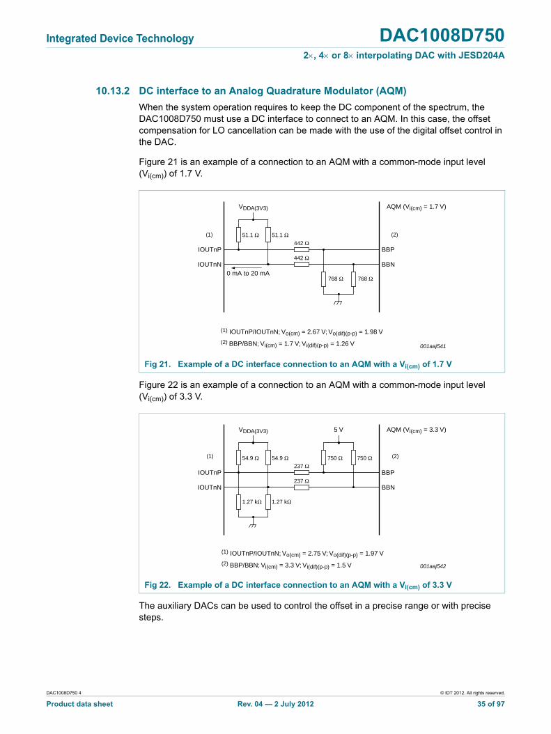
10.13.2 DC interface to an Analog Quadrature Modulator (AQM)
When the system operation requires to keep the DC component of the spectrum, the DAC1008D750 must use a DC interface to connect to an AQM. In this case, the offset compensation for LO cancellation can be made with the use of the digital offset control in the DAC.
Figure 21 is an example of a connection to an AQM with a common-mode input level (Vi(cm)) of 1.7 V.
Figure 22 is an example of a connection to an AQM with a common-mode input level (Vi(cm)) of 3.3 V.
The auxiliary DACs can be used to control the offset in a precise range or with precise steps.
Fig 21. Example of a DC interface connection to an AQM with a Vi(cm) of 1.7 V
Fig 22. Example of a DC interface connection to an AQM with a Vi(cm) of 3.3 V
001aaj541
51.1 Ω 51.1 Ω442 Ω
442 Ω
VDDA(3V3)
IOUTnP
IOUTnN0 mA to 20 mA
BBP
(1) IOUTnP/IOUTnN; Vo(cm) = 2.67 V; Vo(dif)(p-p) = 1.98 V
(2) BBP/BBN; Vi(cm) = 1.7 V; Vi(dif)(p-p) = 1.26 V
BBN
AQM (Vi(cm) = 1.7 V)
768 Ω 768 Ω
(1) (2)
001aaj542
54.9 Ω 54.9 Ω237 Ω
237 Ω
VDDA(3V3)
IOUTnP
IOUTnN
BBP
BBN
AQM (Vi(cm) = 3.3 V)
750 Ω 750 Ω
5 V
1.27 kΩ 1.27 kΩ
(1) IOUTnP/IOUTnN; Vo(cm) = 2.75 V; Vo(dif)(p-p) = 1.97 V
(2) BBP/BBN; Vi(cm) = 3.3 V; Vi(dif)(p-p) = 1.5 V
(1) (2)
DAC1008D750 4 © IDT 2012. All rights reserved.
Product data sheet Rev. 04 — 2 July 2012 35 of 97

Integrated Device Technology DAC1008D7502, 4 or 8 interpolating DAC with JESD204A
Figure 23 is an example of a DC interface connected to an AQM with a common-mode input level (Vi(cm)) of 1.7 V when using auxiliary DACs.
Figure 24 is an example of a DC interface connected to an AQM with a common-mode input level (Vi(cm)) of 3.3 V when using auxiliary DACs.
The constraints to adjusting the interface are the output compliance range of the DAC and the auxiliary DACs, the input common-mode level of the AQM, and the range of offset correction.
Fig 23. Example of a DC interface connection to an AQM with a Vi(cm) of 1.7 V when using auxiliary DACs
Fig 24. Example of a DC interface connection to an AQM with a Vi(cm) of 3.3 V when using auxiliary DACs
001aaj543
51.1 Ω 51.1 Ω442 Ω
442 Ω
VDDA(3V3)
IOUTnP
IOUTnN0 mA to 20 mA
BBP
BBN
AQM (Vi(cm) = 1.7 V)
698 Ω 698 Ω
51.1 Ω 51.1 Ω
AUXnP
AUXnN1.1 mA (typ.)
(1) IOUTnP/IOUTnN; Vo(cm) = 2.67 V; Vo(dif)(p-p) = 1.94 V
(2) BBP/BBN; Vi(cm) = 1.7 V; Vi(dif)(p-p) = 1.23 V; offset correction up to 36 mV
(1) (2)
001aaj544
54.9 Ω 54.9 Ω237 Ω
237 Ω
3.3 V
IOUTnP
IOUTnN
AUXnP
AUXnN
BBP
BBN
AQM (Vi(cm) = 3.3 V)
750 Ω 750 Ω
5 V
634 Ω 634 Ω
442 Ω 442 Ω
(1) IOUTnP/IOUTnN; Vo(cm) = 2.75 V; Vo(dif)(p-p) = 1.96 V
(2) BBP/BBN; Vi(cm) = 3.3 V; Vi(dif)(p-p) = 1.5 V; offset correction up to 36 mV
(1) (2)
DAC1008D750 4 © IDT 2012. All rights reserved.
Product data sheet Rev. 04 — 2 July 2012 36 of 97
Integrated Device Technology DAC1008D7502, 4 or 8 interpolating DAC with JESD204A
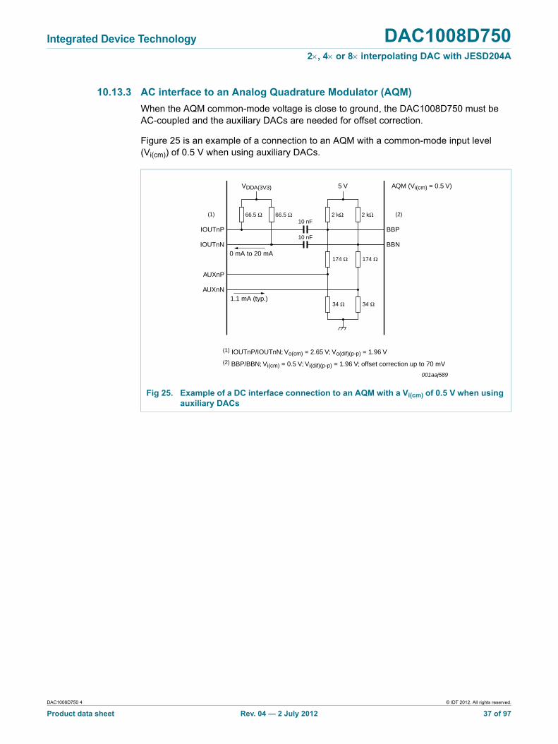
10.13.3 AC interface to an Analog Quadrature Modulator (AQM)
When the AQM common-mode voltage is close to ground, the DAC1008D750 must be AC-coupled and the auxiliary DACs are needed for offset correction.
Figure 25 is an example of a connection to an AQM with a common-mode input level (Vi(cm)) of 0.5 V when using auxiliary DACs.
Fig 25. Example of a DC interface connection to an AQM with a Vi(cm) of 0.5 V when using auxiliary DACs
001aaj589
66.5 Ω 66.5 Ω
10 nF
VDDA(3V3)
IOUTnP
IOUTnN0 mA to 20 mA
BBP
BBN
AQM (Vi(cm) = 0.5 V)
2 kΩ 2 kΩ
5 V
174 Ω 174 Ω
34 Ω 34 Ω
AUXnP
AUXnN1.1 mA (typ.)
10 nF
(1) IOUTnP/IOUTnN; Vo(cm) = 2.65 V; Vo(dif)(p-p) = 1.96 V
(2) BBP/BBN; Vi(cm) = 0.5 V; Vi(dif)(p-p) = 1.96 V; offset correction up to 70 mV
(1) (2)
DAC1008D750 4 © IDT 2012. All rights reserved.
Product data sheet Rev. 04 — 2 July 2012 37 of 97
Integrated Device Technology DAC1008D7502, 4 or 8 interpolating DAC with JESD204A
10.13.4 Phase correction
The Analog Quadrature Modulator which follows the DACs may have a phase imbalance which will result in undesired sidebands. By adjusting the phase between the I and Q channels, the spur can be reduced.
Without compensation the I and Q have a phase difference of / 2 (90). The registers PHASECORR_CNTRL0 and PHASECORR_CNTRL1 located in register page 0 allow a phase variation from 75.7 to 104.3. The two registers define a signed value that ranges from 512 to +511. The resulting phase compensation (in radians) is given by the equation: PHASE_CORR[9:0] / 2048.
10.14 Power and grounding
The power supplies should be decoupled with the following ground pins to optimize the decoupling:
• VDDA(1V8): pin 38 with pin 37; pin 44 with pin 43; pin 11 with pin 12; pin 17 with pin 18; pin 32 with pin 31
10.15 Configuration interface
10.15.1 Register description
DAC1008D750 implements indirect addressing using a page access method. The page-address is located at address 0x1F and is by default 0x00, which selects page 0 as the default page. For example, to access registers which configure the JESDRX, one must first activate page 4 by writing 0x04 to the page-address 0x1F.
The DAC1008D750 contains six different pages.
The device has no embedded power-on-reset feature. Driving the RESET_N pin to set the device to its default state is mandatory.
10.15.2 Detailed descriptions of registers
The register information has been provided in page form accompanied by a detailed description for each bit in the tables following the register allocation map of each page.
DAC1008D750 4 © IDT 2012. All rights reserved.
Product data sheet Rev. 04 — 2 July 2012 38 of 97
xxxxxxxxxxxxxxxxxxxxx xxxxxxxxxxxxxxxxxxxxxxxxxx xxxxxxx x x x xxxxxxxxxxxxxxxxxxxxxxxxxxxxxx xxxxxxxxxxxxxxxxxxx xx xx xxxxx xxxxxxxxxxxxxxxxxxxxxxxxxxx xxxxxxxxxxxxxxxxxxx xxxxxx xxxxxxxxxxxxxxxxxxxxxxxxxxxxxxxxxxx xxxxxxxxxxxx x x xxxxxxxxxxxxxxxxxxxxx xxxxxxxxxxxxxxxxxxxxxxxxxxxxxx xxxxx xxxxxxxxxxxxxxxxxxxxxxxxxxxxxxxxxxxxxxxxxxxxxxxxxx xxxxxxxx xxxxxxxxxxxxxxxxxxxxxxxxx xxxxxxxxxxxxxxxxxxxx xxx
DA
C100
8D750
4
Pro
du
ct data sh
eetR
ev. 04 —
2 July 2012
39 o
f 97
Integ
rated D
evice Techn
olo
gy
DA
C1008D
7502, 4 o
r 8 inte
rpo
lating
DA
C w
ith J
ES
D20
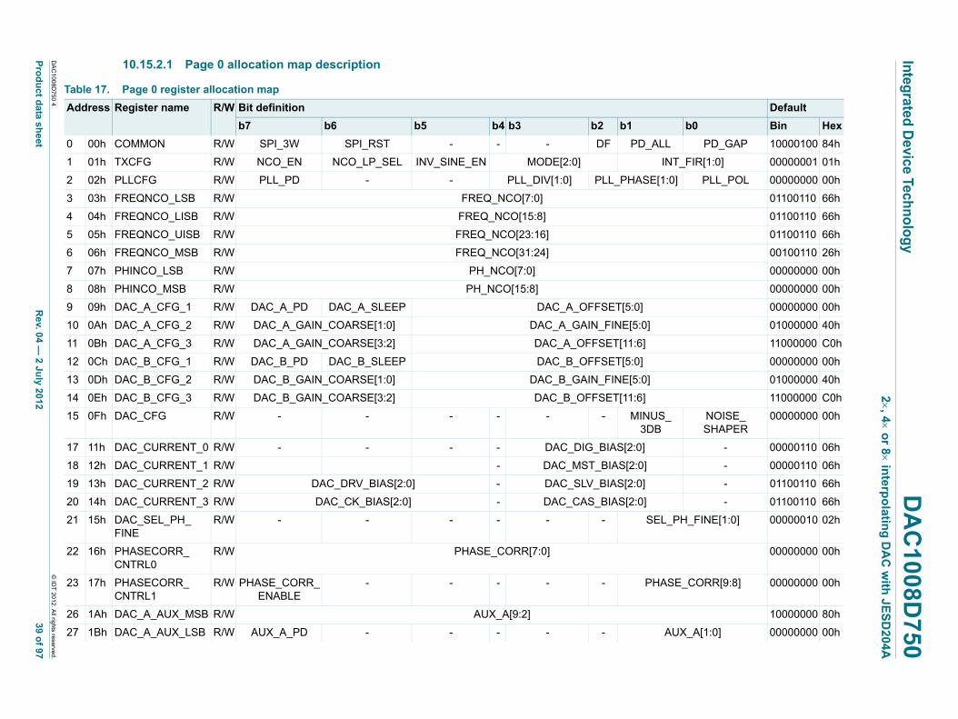
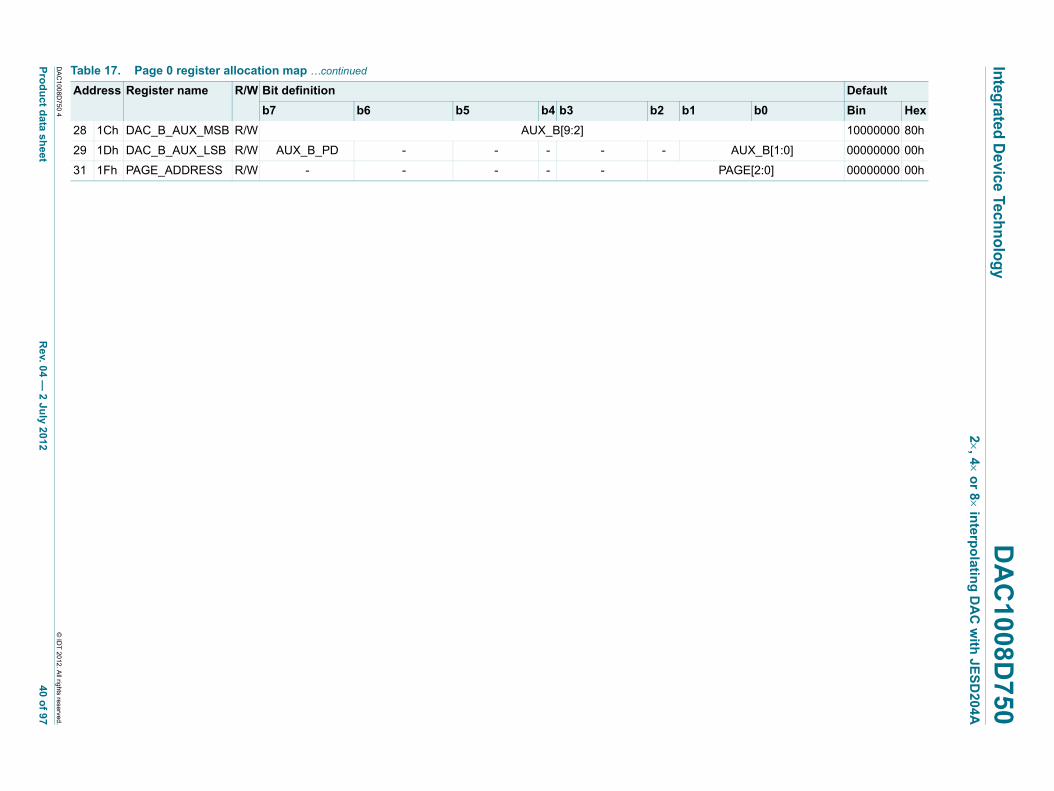
4A10.15.2.1 Page 0 allocation map description
Table 17. Page 0 register allocation map
Default
b0 Bin Hex
PD_GAP 10000100 84h
T_FIR[1:0] 00000001 01h
] PLL_POL 00000000 00h
01100110 66h
01100110 66h
01100110 66h
00100110 26h
00000000 00h
00000000 00h
00000000 00h
01000000 40h
11000000 C0h
00000000 00h
01000000 40h
11000000 C0h
NOISE_SHAPER
00000000 00h
- 00000110 06h
- 00000110 06h
- 01100110 66h
- 01100110 66h
PH_FINE[1:0] 00000010 02h
00000000 00h
E_CORR[9:8] 00000000 00h
10000000 80h
UX_A[1:0] 00000000 00h
© ID
T 20
12. All rights reserved
.
Address Register name R/W Bit definition
b7 b6 b5 b4 b3 b2 b1
0 00h COMMON R/W SPI_3W SPI_RST - - - DF PD_ALL
1 01h TXCFG R/W NCO_EN NCO_LP_SEL INV_SINE_EN MODE[2:0] IN
2 02h PLLCFG R/W PLL_PD - - PLL_DIV[1:0] PLL_PHASE[1:0
3 03h FREQNCO_LSB R/W FREQ_NCO[7:0]
4 04h FREQNCO_LISB R/W FREQ_NCO[15:8]
5 05h FREQNCO_UISB R/W FREQ_NCO[23:16]
6 06h FREQNCO_MSB R/W FREQ_NCO[31:24]
7 07h PHINCO_LSB R/W PH_NCO[7:0]
8 08h PHINCO_MSB R/W PH_NCO[15:8]
9 09h DAC_A_CFG_1 R/W DAC_A_PD DAC_A_SLEEP DAC_A_OFFSET[5:0]
10 0Ah DAC_A_CFG_2 R/W DAC_A_GAIN_COARSE[1:0] DAC_A_GAIN_FINE[5:0]
11 0Bh DAC_A_CFG_3 R/W DAC_A_GAIN_COARSE[3:2] DAC_A_OFFSET[11:6]
12 0Ch DAC_B_CFG_1 R/W DAC_B_PD DAC_B_SLEEP DAC_B_OFFSET[5:0]
13 0Dh DAC_B_CFG_2 R/W DAC_B_GAIN_COARSE[1:0] DAC_B_GAIN_FINE[5:0]
14 0Eh DAC_B_CFG_3 R/W DAC_B_GAIN_COARSE[3:2] DAC_B_OFFSET[11:6]
15 0Fh DAC_CFG R/W - - - - - - MINUS_3DB
17 11h DAC_CURRENT_0 R/W - - - - DAC_DIG_BIAS[2:0]
18 12h DAC_CURRENT_1 R/W - DAC_MST_BIAS[2:0]
19 13h DAC_CURRENT_2 R/W DAC_DRV_BIAS[2:0] - DAC_SLV_BIAS[2:0]
20 14h DAC_CURRENT_3 R/W DAC_CK_BIAS[2:0] - DAC_CAS_BIAS[2:0]
21 15h DAC_SEL_PH_FINE
R/W - - - - - - SEL_
22 16h PHASECORR_CNTRL0
R/W PHASE_CORR[7:0]
23 17h PHASECORR_CNTRL1
R/W PHASE_CORR_ENABLE
- - - - - PHAS
26 1Ah DAC_A_AUX_MSB R/W AUX_A[9:2]
27 1Bh DAC_A_AUX_LSB R/W AUX_A_PD - - - - - A
xxxxxxxxxxxxxxxxxxxxx xxxxxxxxxxxxxxxxxxxxxxxxxx xxxxxxx x x x xxxxxxxxxxxxxxxxxxxxxxxxxxxxxx xxxxxxxxxxxxxxxxxxx xx xx xxxxx xxxxxxxxxxxxxxxxxxxxxxxxxxx xxxxxxxxxxxxxxxxxxx xxxxxx xxxxxxxxxxxxxxxxxxxxxxxxxxxxxxxxxxx xxxxxxxxxxxx x x xxxxxxxxxxxxxxxxxxxxx xxxxxxxxxxxxxxxxxxxxxxxxxxxxxx xxxxx xxxxxxxxxxxxxxxxxxxxxxxxxxxxxxxxxxxxxxxxxxxxxxxxxx xxxxxxxx xxxxxxxxxxxxxxxxxxxxxxxxx xxxxxxxxxxxxxxxxxxxx xxx
DA
C100
8D750
4
Pro
du
ct data sh
eetR
ev. 04 —
2 July 2012
40 o
f 97
Integ
rated D
evice Techn
olo
gy
DA
C1008D
7502, 4 o
r 8 inte
rpo
lating
DA
C w
ith J
ES
D20
4A
10000000 80h
UX_B[1:0] 00000000 00h
E[2:0] 00000000 00h
Table 17. Page 0 register allocation map …continued
Address Register name R/W Bit definition Default
b7 b6 b5 b4 b3 b2 b1 b0 Bin Hex
© ID
T 20
12. All rights reserved
.
28 1Ch DAC_B_AUX_MSB R/W AUX_B[9:2]
29 1Dh DAC_B_AUX_LSB R/W AUX_B_PD - - - - - A
31 1Fh PAGE_ADDRESS R/W - - - - - PAG
Integrated Device Technology DAC1008D7502, 4 or 8 interpolating DAC with JESD204A
10.15.2.2 Page 0 bit definition detailed description
Please refer to Table 17 for a register overview for page 0. In the following tables, all the values emphasized in bold are the default values.
Table 18. COMMON register (address 00h) bit descriptionDefault settings are shown highlighted.
Bit Symbol Access Value Description
7 SPI_3W R/W serial interface bus type
0 4 wire SPI
1 3 wire SPI
6 SPI_RST R/W serial interface reset
0 no reset
1 performs a reset on all registers except 0x00
2 DF R/W data format
0 signed (two’s compliment) format
1 unsigned format
1 PD_ALL R/W power-down
0 no action
1 all circuits (digital and analog) are switched off
0 GAP_PD R/W internal bandgap power-down
0 no action
1 internal bandgap references are switched off
Table 19. TXCFG register (address 01h) bit descriptionDefault settings are shown highlighted.
Bit Symbol Access Value Description
7 NCO_EN R/W NCO
0 disabled (the NCO phase is reset to 0)
1 enabled
6 NCO_LP_SEL R/W low-power NCO
0 NCO may use all 32 bits
1 NCO frequency and phase given by the five MSBs of the registers 06h and 08h respectively
5 INV_SINE_EN R/W x / (sin x) function
0 disabled
1 enabled
4 to 2 MODE[2:0] R/W modulation
000 dual DAC: no modulation
001 positive upper single sideband up-conversion
010 positive lower single sideband up-conversion
011 negative upper single sideband up-conversion
100 negative lower single sideband up-conversion
DAC1008D750 4 © IDT 2012. All rights reserved.
Product data sheet Rev. 04 — 2 July 2012 41 of 97
Integrated Device Technology DAC1008D7502, 4 or 8 interpolating DAC with JESD204A
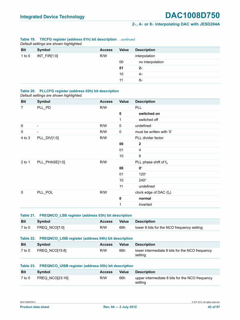
1 to 0 INT_FIR[1:0] R/W interpolation
00 no interpolation
01 2
10 4
11 8
Table 19. TXCFG register (address 01h) bit description …continuedDefault settings are shown highlighted.
Bit Symbol Access Value Description
Table 20. PLLCFG register (address 02h) bit descriptionDefault settings are shown highlighted.
Bit Symbol Access Value Description
7 PLL_PD R/W PLL
0 switched on
1 switched off
6 - R/W 0 undefined
5 - R/W 0 must be written with ’0’
4 to 3 PLL_DIV[1:0] R/W PLL divider factor
00 2
01 4
10 8
2 to 1 PLL_PHASE[1:0] R/W PLL phase shift of fs
00 0
01 120
10 240
11 undefined
0 PLL_POL R/W clock edge of DAC (fs)
0 normal
1 inverted
Table 21. FREQNCO_LSB register (address 03h) bit description
Bit Symbol Access Value Description
7 to 0 FREQ_NCO[7:0] R/W 66h lower 8 bits for the NCO frequency setting
Table 22. FREQNCO_LISB register (address 04h) bit description
Bit Symbol Access Value Description
7 to 0 FREQ_NCO[15:8] R/W 66h lower intermediate 8 bits for the NCO frequency setting
Table 23. FREQNCO_UISB register (address 05h) bit description
Bit Symbol Access Value Description
7 to 0 FREQ_NCO[23:16] R/W 66h upper intermediate 8 bits for the NCO frequency setting
DAC1008D750 4 © IDT 2012. All rights reserved.
Product data sheet Rev. 04 — 2 July 2012 42 of 97
Integrated Device Technology DAC1008D7502, 4 or 8 interpolating DAC with JESD204A
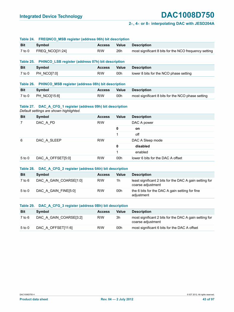
Table 24. FREQNCO_MSB register (address 06h) bit description
Bit Symbol Access Value Description
7 to 0 FREQ_NCO[31:24] R/W 26h most significant 8 bits for the NCO frequency setting
Table 25. PHINCO_LSB register (address 07h) bit description
Bit Symbol Access Value Description
7 to 0 PH_NCO[7:0] R/W 00h lower 8 bits for the NCO phase setting
Table 26. PHINCO_MSB register (address 08h) bit description
Bit Symbol Access Value Description
7 to 0 PH_NCO[15:8] R/W 00h most significant 8 bits for the NCO phase setting
Table 27. DAC_A_CFG_1 register (address 09h) bit descriptionDefault settings are shown highlighted.
Bit Symbol Access Value Description
7 DAC_A_PD R/W DAC A power
0 on
1 off
6 DAC_A_SLEEP R/W DAC A Sleep mode
0 disabled
1 enabled
5 to 0 DAC_A_OFFSET[5:0] R/W 00h lower 6 bits for the DAC A offset
Table 28. DAC_A_CFG_2 register (address 0Ah) bit description
Bit Symbol Access Value Description
7 to 6 DAC_A_GAIN_COARSE[1:0] R/W 1h least significant 2 bits for the DAC A gain setting for coarse adjustment
5 to 0 DAC_A_GAIN_FINE[5:0] R/W 00h the 6 bits for the DAC A gain setting for fine adjustment
Table 29. DAC_A_CFG_3 register (address 0Bh) bit description
Bit Symbol Access Value Description
7 to 6 DAC_A_GAIN_COARSE[3:2] R/W 3h most significant 2 bits for the DAC A gain setting for coarse adjustment
5 to 0 DAC_A_OFFSET[11:6] R/W 00h most significant 6 bits for the DAC A offset
DAC1008D750 4 © IDT 2012. All rights reserved.
Product data sheet Rev. 04 — 2 July 2012 43 of 97

Integrated Device Technology DAC1008D7502, 4 or 8 interpolating DAC with JESD204A
Table 30. DAC_B_CFG_1 register (address 0Ch) bit descriptionDefault settings are shown highlighted.
Bit Symbol Access Value Description
7 DAC_B_PD R/W DAC B power
0 on
1 off
6 DAC_B_SLEEP R/W DAC B Sleep mode
0 disabled
1 enabled
5 to 0 DAC_B_OFFSET[5:0] R/W 00h lower 6 bits for the DAC B offset
Table 31. DAC_B_CFG_2 register (address 0Dh) bit description
Bit Symbol Access Value Description
7 to 6 DAC_B_GAIN_COARSE[1:0] R/W 1h least significant 2 bits for the DAC B gain setting for coarse adjustment
5 to 0 DAC_B_GAIN_FINE[5:0] R/W 00h the 6 bits for the DAC B gain setting for fine adjustment
Table 32. DAC_B_CFG_3 register (address 0Eh) bit description
Bit Symbol Access Value Description
7 to 6 DAC_B_GAIN_COARSE[3:2] R/W 3h most significant 2 bits for the DAC B gain setting for coarse adjustment
5 to 0 DAC_B_OFFSET[11:6] R/W 00h most significant 6 bits for the DAC B offset
Table 33. DAC_CFG register (address 0Fh) bit descriptionDefault settings are shown highlighted.
Bit Symbol Access Value Description
1 MINUS_3DB R/W NCO gain
0 unity
1 3 dB
0 NOISE_SHAPER R/W noise shaper
0 disabled
1 enabled
Table 34. DAC_CURRENT_0 register (address 11h) bit descriptionDefault settings are shown highlighted.
Bit Symbol Access Value Description
3 to 1 DAC_DIG_BIAS[2:0] R/W 3h bias current control (see Table 46)
Table 35. DAC_CURRENT_1 register (address 12h) bit descriptionDefault settings are shown highlighted.
Bit Symbol Access Value Description
3 to 1 DAC_MST_BIAS[2:0] R/W 3h bias current control (see Table 46)
DAC1008D750 4 © IDT 2012. All rights reserved.
Product data sheet Rev. 04 — 2 July 2012 44 of 97

Integrated Device Technology DAC1008D7502, 4 or 8 interpolating DAC with JESD204A
Table 36. DAC_CURRENT_2 register (address 13h) bit descriptionDefault settings are shown highlighted.
Bit Symbol Access Value Description
7 to 5 DAC_DRV_BIAS[2:0] R/W 3h bias current control (see Table 46)
3 to 1 DAC_SLV_BIAS[2:0] R/W 3h bias current control (see Table 46)
Table 37. DAC_CURRENT_3 register (address 14h) bit descriptionDefault settings are shown highlighted.
Bit Symbol Access Value Description
7 to 5 DAC_CK_BIAS[2:0] R/W 3h bias current control (see Table 46)
3 to 1 DAC_CAS_BIAS[2:0] R/W 3h bias current control (see Table 46)
Table 38. DAC_SEL_PH_FINE register (address 15h) bit descriptionDefault settings are shown highlighted.
Bit Symbol Access Value Description
1 to 0 SEL_PH_FINE[1:0] R/W 2h fine DAC phase selection
Table 39. PHASECORR_CNTRL0 register (address 16h) bit descriptionDefault settings are shown highlighted.
Bit Symbol Access Value Description
7 to 0 PHASE_CORR[7:0] R/W 00h LSB phase correction factor
Table 40. PHASECORR_CNTRL1 register (address 17h) bit descriptionDefault settings are shown highlighted.
Bit Symbol Access Value Description
7 PHASE_CORR_ENABLE R/W phase correction
0 disabled
1 enabled
1 to 0 PHASE_CORR[9:8] R/W 0h MSB phase correction factor
Table 41. DAC_A_AUX_MSB register (address 1Ah) bit description
Bit Symbol Access Value Description
7 to 0 AUX_A[9:2] R/W 80h most significant 8 bits for auxiliary DAC A
Table 42. DAC_A_AUX_LSB register (address 1Bh) bit descriptionDefault settings are shown highlighted.
Bit Symbol Access Value Description
7 AUX_A_PD R/W auxiliary DAC A power
0 on
1 off
1 to 0 AUX_A[1:0] R/W 0h lower 2 bits for auxiliary DAC A
Table 43. DAC_B_AUX_MSB register (address 1Ch) bit description
Bit Symbol Access Value Description
7 to 0 AUX_B[9:2] R/W 80h most significant 8 bits for auxiliary DAC B
DAC1008D750 4 © IDT 2012. All rights reserved.
Product data sheet Rev. 04 — 2 July 2012 45 of 97
Integrated Device Technology DAC1008D7502, 4 or 8 interpolating DAC with JESD204A
Table 44. DAC_B_AUX_LSB register (address 1Dh) bit descriptionDefault settings are shown highlighted.
Bit Symbol Access Value Description
7 AUX_B_PD R/W auxiliary DAC B power
0 on
1 off
1 to 0 AUX_B[1:0] R/W 0h lower 2 bits for auxiliary DAC B
Table 45. DAC_B_AUX_LSB register (address 1Dh) bit descriptionDefault settings are shown highlighted.
Bit Symbol Access Value Description
2 to 0 PAGE[2:0] R/W 0h page address
Table 46. Bias current control tableDefault settings are shown highlighted.
BIAS[2:0] Deviation from nominal current
000 30 %
001 ...
010 ...
011 0 %
100 ...
101 ...
110 ...
111 +30 %
DAC1008D750 4 © IDT 2012. All rights reserved.
Product data sheet Rev. 04 — 2 July 2012 46 of 97

xxxxxxxxxxxxxxxxxxxxx xxxxxxxxxxxxxxxxxxxxxxxxxx xxxxxxx x x x xxxxxxxxxxxxxxxxxxxxxxxxxxxxxx xxxxxxxxxxxxxxxxxxx xx xx xxxxx xxxxxxxxxxxxxxxxxxxxxxxxxxx xxxxxxxxxxxxxxxxxxx xxxxxx xxxxxxxxxxxxxxxxxxxxxxxxxxxxxxxxxxx xxxxxxxxxxxx x x xxxxxxxxxxxxxxxxxxxxx xxxxxxxxxxxxxxxxxxxxxxxxxxxxxx xxxxx xxxxxxxxxxxxxxxxxxxxxxxxxxxxxxxxxxxxxxxxxxxxxxxxxx xxxxxxxx xxxxxxxxxxxxxxxxxxxxxxxxx xxxxxxxxxxxxxxxxxxxx xxx
DA
C100
8D750
4
Pro
du
ct data sh
eetR
ev. 04 —
2 July 2012
47 o
f 97
Integ
rated D
evice Techn
olo
gy
DA
C1008D
7502, 4 o
r 8 inte
rpo
lating
DA
C w
ith J
ES
D20
4A10.15.2.3 Page 1 allocation map description
Table 47. Page 1 register allocation map
Default[1]
b0 Bin Hex
S_TER
MDS_ENA
00000100 04h
10000000 80h
01000000 40h
WIDTH[2:0] 00010000 10h
01000000 40h
10000000 80h
[3:0] 00001111 0Fh
uuuuuuuu uuh
AL_ND
MDS_ACTIVE
uuuuuuuu uuh
S_OUT
MDS_LOCK
uuuuuuuu uuh
[2:0] 00000000 00h
© ID
T 20
12. All rights reserved
.
[1] u = undefined at power-up or after reset.
Address Register name R/W Bit definition
b7 b6 b5 b4 b3 b2 b1
0 00h MDS_MAIN R/W MDS_EQCHECK[1:0] MDS_RUN
MDS_NCO MDS_SEL_LN23
MDS_32T_ENA
MDMAS
1 01h MDS_WIN_PERIOD_A R/W MDS_WIN_PERIOD_A[7:0]
2 02h MDS_WIN_PERIOD_B R/W MDS_WIN_PERIOD_B[7:0]
3 03h MDS_MISCCNTRL0 R/W - - - MDS_EVAL_ENA
MDS_PRERUN_
ENA
MDS_PULSE
4 04h MDS_MAN_ADJUSTDLY
R/W MDS_MAN
MDS_MAN_ADJUSTDLY[6:0]
5 05h MDS_AUTO_CYCLES R/W MDS_AUTO_CYCLES[7:0]
6 06h MDS_MISCCNTRL1 R/W MDS_SR_CKEN
MDS_SR_LOCKOUT
MDS_SR_
LOCK
MDS_RELOCK
MDS_LOCK_DELAY
8 08h MDS_ADJDELAY R - MDS_ADJDELAY[6:0]
9 09h MDS_STATUS0 R EARLY LATE EQUAL MDS_LOCK EARLY_ERROR
LATE_ERROR
EQUFOU
10 0Ah MDS_STATUS1 R - - - - JD_ODD MDS_PRERUN
MDLOCK
31 1Fh PAGE_ADDRESS R/W - - - - - PAGE
Integrated Device Technology DAC1008D7502, 4 or 8 interpolating DAC with JESD204A
10.15.2.4 Page 1 bit definition detailed description
Please refer to Table 47 for a register overview and their default values. In the following tables, all the values emphasized in bold are the default values.
Table 48. MDS_MAIN register (address 00h) bit descriptionDefault settings are shown highlighted.
Bit Symbol Access Value Description
7 to 6 MDS_EQCHECK[1:0] R/W lock mode
00 lock when (early = 1 and late = 1)
01 lock when (early = 1 and late = 1 and equal = 1)
10 lock when equal = 1
11 force_lock (equal-check = 1)
5 MDS_RUN R/W evaluation restart
0 no action
1 transition from 0 to 1 restarts evaluation_counter
4 MDS_NCO R/W NCO synchronization
0 no action
1 NCO synchronization enabled
3 MDS_SEL_LN23 R/W synchronization reference
0 use lane 1 enable as reference for synchronization
1 use lane 2/lane 3 enable as reference for synchronization
2 MDS_32T_ENA R/W maximum delay
0 maximum coarse delay is 16T_dclk
1 maximum coarse delay is 32T_dclk
1 MDS_MASTER R/W MDS mode
0 slave mode
1 master mode
0 MDS_ENA R/W MDS function
0 disable MDS function
1 enable MDS function
Table 49. MDS_WIN_PERIOD_A register (address 01h) bit descriptionDefault settings are shown highlighted.
Bit Symbol Access Value Description
7 to 0 MDS_WIN_PERIOD_A[7:0] R/W 80h determines MDS window LOW-time
Table 50. MDS_WIN_PERIOD_B register (address 02h) bit descriptionDefault settings are shown highlighted.
Bit Symbol Access Value Description
7 to 0 MDS_WIN_PERIOD_B[7:0] R/W 40h determines MDS window HIGH-time
DAC1008D750 4 © IDT 2012. All rights reserved.
Product data sheet Rev. 04 — 2 July 2012 48 of 97
Integrated Device Technology DAC1008D7502, 4 or 8 interpolating DAC with JESD204A
Table 51. MDS_MISCCNTRL0 register (address 03h) bit descriptionDefault settings are shown highlighted.
Bit Symbol Access Value Description
4 MDS_EVAL_ENA R/W MDS evaluation
0 disabled
1 enabled
3 MDS_PRERUN_ENA R/W automatic MDS start-up
0 no mds_win/mds_ref generation in advance
1 mds_win/mds_ref run-in before MDS evaluation
2 to 0 MDS_PULSEWIDTH[2:0] R/W width of MDS (in output clk-periods)
000 1T
001 2T
010 to 111
(MDS_pulsewidth 1) 4T
Table 52. MDS_MAN_ADJUSTDLY register (address 04h) bit descriptionDefault settings are shown highlighted.
Bit Symbol Access Value Description
7 MDS_MAN R/W adjustment delay mode
0 auto-control adjustment delays
1 manual control adjustment delays
6 to 0 MDS_MAN_ADJUSTDLY[6:0] R/W adjustment delay value
40h if MDS_MAN = 0 then initial value adjustment delay
- if MDS_MAN = 1 then controls adjustment delay
Table 53. MDS_AUTO_CYCLES register (address 05h) bit descriptionDefault settings are shown highlighted.
Bit Symbol Access Value Description
7 to 0 MDS_AUTO_CYCLES[7:0] R/W 80h number of evaluation cycles applied for MDS
Table 54. MDS_MISCCNTRL1 register (address 06h) bit descriptionDefault settings are shown highlighted.
Bit Symbol Access Value Description
7 MDS_SR_CKEN R/W lock mode
0 free-running mds_cken
1 MDS_CKEN forced LOW
6 MDS_SR_LOCKOUT R/W lockout detector soft reset
0 MDS_SR_LOCKOUT in use
1 MDS_SR_LOCKOUT forced LOW
5 MDS_SR_LOCK R/W lock detector soft reset
0 MDS_SR_LOCK in use
1 MDS_SR_LOCK forced LOW
DAC1008D750 4 © IDT 2012. All rights reserved.
Product data sheet Rev. 04 — 2 July 2012 49 of 97
Integrated Device Technology DAC1008D7502, 4 or 8 interpolating DAC with JESD204A
4 MDS_RELOCK R/W relock mode
0 no action
1 relock when lockout occurs
3 to 0 MDS_LOCK_DELAY[3:0] R/W Fh number of succeeding 'equal'-detections until lock
Table 54. MDS_MISCCNTRL1 register (address 06h) bit description …continuedDefault settings are shown highlighted.
Bit Symbol Access Value Description
Table 55. MDS_ADJDELAY register (address 08h) bit descriptionDefault settings are shown highlighted.
Bit Symbol Access Value Description
6 to 0 MDS_ADJDELAY[6:0] R - actual value adjustment delay
Table 56. MDS_STATUS0 register (address 09h) bit descriptionDefault settings are shown highlighted.
Bit Symbol Access Value Description
7 EARLY R early signal (sampled) from early-late detector
0 false
1 true
6 LATE R late signal (sampled) from early-late detector
0 false
1 true
5 EQUAL R equal signal (sampled) from early-late detector
0 false
1 true
4 MDS_LOCK R result equal check
0 false
1 true
3 EARLY_ERROR R adjustment delay maximum value stops the search
0 false
1 true
2 LATE_ERROR R adjustment delay minimum value stops the search
0 false
1 true
1 EQUAL_FOUND R evaluation logic has detected equal condition
0 false
1 true
0 MDS_ACTIVE R evaluation logic active
0 false
1 true
DAC1008D750 4 © IDT 2012. All rights reserved.
Product data sheet Rev. 04 — 2 July 2012 50 of 97
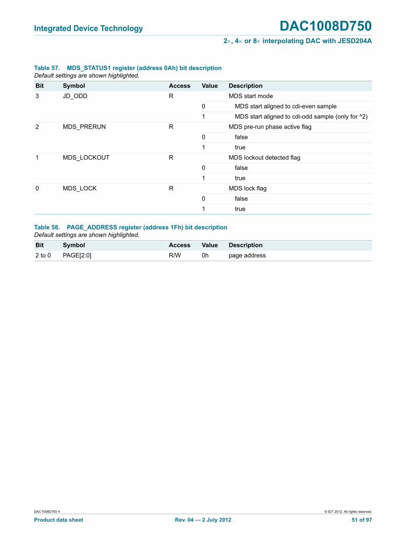
Integrated Device Technology DAC1008D7502, 4 or 8 interpolating DAC with JESD204A
Table 57. MDS_STATUS1 register (address 0Ah) bit descriptionDefault settings are shown highlighted.
Bit Symbol Access Value Description
3 JD_ODD R MDS start mode
0 MDS start aligned to cdi-even sample
1 MDS start aligned to cdi-odd sample (only for ^2)
2 MDS_PRERUN R MDS pre-run phase active flag
0 false
1 true
1 MDS_LOCKOUT R MDS lockout detected flag
0 false
1 true
0 MDS_LOCK R MDS lock flag
0 false
1 true
Table 58. PAGE_ADDRESS register (address 1Fh) bit descriptionDefault settings are shown highlighted.
Bit Symbol Access Value Description
2 to 0 PAGE[2:0] R/W 0h page address
DAC1008D750 4 © IDT 2012. All rights reserved.
Product data sheet Rev. 04 — 2 July 2012 51 of 97
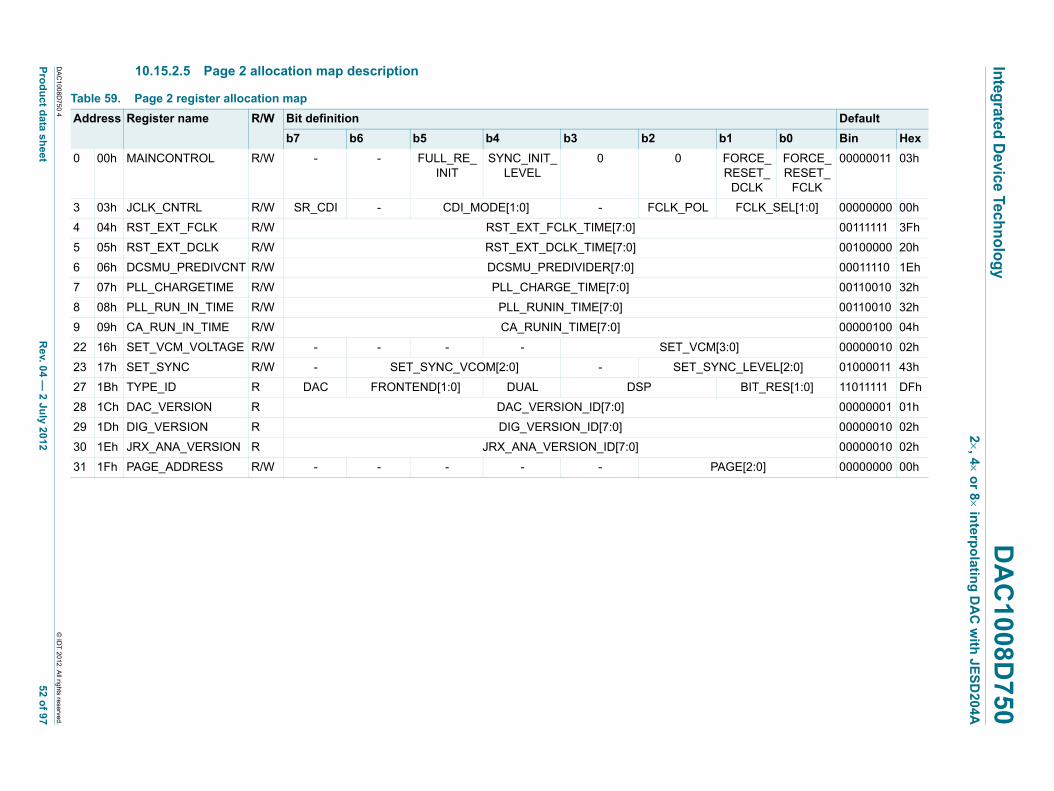
xxxxxxxxxxxxxxxxxxxxx xxxxxxxxxxxxxxxxxxxxxxxxxx xxxxxxx x x x xxxxxxxxxxxxxxxxxxxxxxxxxxxxxx xxxxxxxxxxxxxxxxxxx xx xx xxxxx xxxxxxxxxxxxxxxxxxxxxxxxxxx xxxxxxxxxxxxxxxxxxx xxxxxx xxxxxxxxxxxxxxxxxxxxxxxxxxxxxxxxxxx xxxxxxxxxxxx x x xxxxxxxxxxxxxxxxxxxxx xxxxxxxxxxxxxxxxxxxxxxxxxxxxxx xxxxx xxxxxxxxxxxxxxxxxxxxxxxxxxxxxxxxxxxxxxxxxxxxxxxxxx xxxxxxxx xxxxxxxxxxxxxxxxxxxxxxxxx xxxxxxxxxxxxxxxxxxxx xxx
DA
C100
8D750
4
Pro
du
ct data sh
eetR
ev. 04 —
2 July 2012
52 o
f 97
Integ
rated D
evice Techn
olo
gy
DA
C1008D
7502, 4 o
r 8 inte
rpo
lating
DA
C w
ith J
ES
D20
4A10.15.2.5 Page 2 allocation map description
Table 59. Page 2 register allocation map
Default
b0 Bin Hex
RCE_SET_CLK
FORCE_RESET_
FCLK
00000011 03h
CLK_SEL[1:0] 00000000 00h
00111111 3Fh
00100000 20h
00011110 1Eh
00110010 32h
00110010 32h
00000100 04h
00000010 02h
LEVEL[2:0] 01000011 43h
BIT_RES[1:0] 11011111 DFh
00000001 01h
00000010 02h
00000010 02h
[2:0] 00000000 00h
© ID
T 20
12. All rights reserved
.
Address Register name R/W Bit definition
b7 b6 b5 b4 b3 b2 b1
0 00h MAINCONTROL R/W - - FULL_RE_INIT
SYNC_INIT_LEVEL
0 0 FORE
D
3 03h JCLK_CNTRL R/W SR_CDI - CDI_MODE[1:0] - FCLK_POL F
4 04h RST_EXT_FCLK R/W RST_EXT_FCLK_TIME[7:0]
5 05h RST_EXT_DCLK R/W RST_EXT_DCLK_TIME[7:0]
6 06h DCSMU_PREDIVCNT R/W DCSMU_PREDIVIDER[7:0]
7 07h PLL_CHARGETIME R/W PLL_CHARGE_TIME[7:0]
8 08h PLL_RUN_IN_TIME R/W PLL_RUNIN_TIME[7:0]
9 09h CA_RUN_IN_TIME R/W CA_RUNIN_TIME[7:0]
22 16h SET_VCM_VOLTAGE R/W - - - - SET_VCM[3:0]
23 17h SET_SYNC R/W - SET_SYNC_VCOM[2:0] - SET_SYNC_
27 1Bh TYPE_ID R DAC FRONTEND[1:0] DUAL DSP
28 1Ch DAC_VERSION R DAC_VERSION_ID[7:0]
29 1Dh DIG_VERSION R DIG_VERSION_ID[7:0]
30 1Eh JRX_ANA_VERSION R JRX_ANA_VERSION_ID[7:0]
31 1Fh PAGE_ADDRESS R/W - - - - - PAGE

Integrated Device Technology DAC1008D7502, 4 or 8 interpolating DAC with JESD204A
10.15.2.6 Page 2 bit definition detailed description
Please refer to Table 59 for a register overview and their default values. In the following tables, all the values emphasized in bold are the default values.
Table 60. MAINCONTROL register (address 00h) bit descriptionDefault settings are shown highlighted.
Bit Symbol Access Value Description
5 FULL_RE_INIT R/W initialization
0 quick reinitialization
1 full reinitialization
4 SYNC_INIT_LEVEL R/W synchronization
0 synchronization starts with '0'
1 synchronization starts with '1'
3 - R/W must be written with ’0’
2 - R/W must be written with ’0’
1 FORCE_RESET_DCLK R/W reset_dclk
0 release reset_dclk
1 force reset_dclk
0 FORCE_RESET_FCLK R/W reset_fclk
0 release reset_fclk
1 force reset_fclk
Table 61. JCLK_CNTRL register (address 03h) bit descriptionDefault settings are shown highlighted.
Bit Symbol Access Value Description
7 SR_CDI R/W cdi reset
0 no action
1 soft reset cdi
5 to 4 CDI_MODE[1:0] R/W cdi mode
00 cdi_mode 0 (^2 modes)
01 cdi_mode 1 (^4 modes)
10 cdi_mode 2 (^8 modes)
11 reserved
2 FCLK_POL R/W fclk polarity
0 no action
1 invert polarity
1 to 0 FCLK_SEL[1:0] R/W fclk clock source
00 dclk 2
01 dclk
10 dclk_div2; running
11 dclk_div2; reset dclk_div2 divider
DAC1008D750 4 © IDT 2012. All rights reserved.
Product data sheet Rev. 04 — 2 July 2012 53 of 97
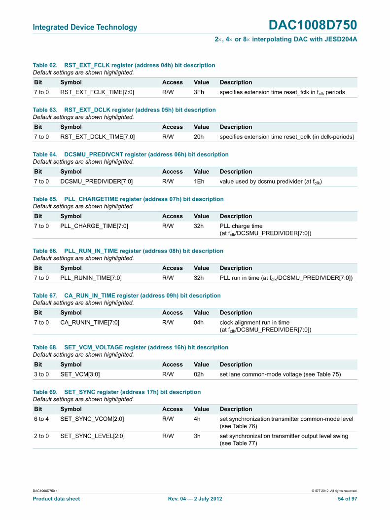
Integrated Device Technology DAC1008D7502, 4 or 8 interpolating DAC with JESD204A
Table 62. RST_EXT_FCLK register (address 04h) bit descriptionDefault settings are shown highlighted.
Bit Symbol Access Value Description
7 to 0 RST_EXT_FCLK_TIME[7:0] R/W 3Fh specifies extension time reset_fclk in fclk periods
Table 63. RST_EXT_DCLK register (address 05h) bit descriptionDefault settings are shown highlighted.
Bit Symbol Access Value Description
7 to 0 RST_EXT_DCLK_TIME[7:0] R/W 20h specifies extension time reset_dclk (in dclk-periods)
Table 64. DCSMU_PREDIVCNT register (address 06h) bit descriptionDefault settings are shown highlighted.
Bit Symbol Access Value Description
7 to 0 DCSMU_PREDIVIDER[7:0] R/W 1Eh value used by dcsmu predivider (at fclk)
Table 65. PLL_CHARGETIME register (address 07h) bit descriptionDefault settings are shown highlighted.
Bit Symbol Access Value Description
7 to 0 PLL_CHARGE_TIME[7:0] R/W 32h PLL charge time (at fclk/DCSMU_PREDIVIDER[7:0])
Table 66. PLL_RUN_IN_TIME register (address 08h) bit descriptionDefault settings are shown highlighted.
Bit Symbol Access Value Description
7 to 0 PLL_RUNIN_TIME[7:0] R/W 32h PLL run in time (at fclk/DCSMU_PREDIVIDER[7:0])
Table 67. CA_RUN_IN_TIME register (address 09h) bit descriptionDefault settings are shown highlighted.
Bit Symbol Access Value Description
7 to 0 CA_RUNIN_TIME[7:0] R/W 04h clock alignment run in time (at fclk/DCSMU_PREDIVIDER[7:0])
Table 68. SET_VCM_VOLTAGE register (address 16h) bit descriptionDefault settings are shown highlighted.
Bit Symbol Access Value Description
3 to 0 SET_VCM[3:0] R/W 02h set lane common-mode voltage (see Table 75)
Table 69. SET_SYNC register (address 17h) bit descriptionDefault settings are shown highlighted.
Bit Symbol Access Value Description
6 to 4 SET_SYNC_VCOM[2:0] R/W 4h set synchronization transmitter common-mode level (see Table 76)
2 to 0 SET_SYNC_LEVEL[2:0] R/W 3h set synchronization transmitter output level swing (see Table 77)
DAC1008D750 4 © IDT 2012. All rights reserved.
Product data sheet Rev. 04 — 2 July 2012 54 of 97
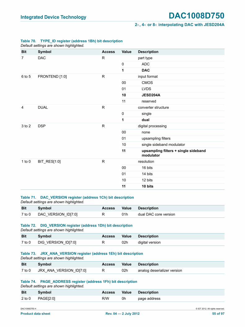
Integrated Device Technology DAC1008D7502, 4 or 8 interpolating DAC with JESD204A
Table 70. TYPE_ID register (address 1Bh) bit descriptionDefault settings are shown highlighted.
Bit Symbol Access Value Description
7 DAC R part type
0 ADC
1 DAC
6 to 5 FRONTEND [1:0] R input format
00 CMOS
01 LVDS
10 JESD204A
11 reserved
4 DUAL R converter structure
0 single
1 dual
3 to 2 DSP R digital processing
00 none
01 upsampling filters
10 single sideband modulator
11 upsampling filters + single sideband modulator
1 to 0 BIT_RES[1:0] R resolution
00 16 bits
01 14 bits
10 12 bits
11 10 bits
Table 71. DAC_VERSION register (address 1Ch) bit descriptionDefault settings are shown highlighted.
Bit Symbol Access Value Description
7 to 0 DAC_VERSION_ID[7:0] R 01h dual DAC core version
Table 72. DIG_VERSION register (address 1Dh) bit descriptionDefault settings are shown highlighted.
Bit Symbol Access Value Description
7 to 0 DIG_VERSION_ID[7:0] R 02h digital version
Table 73. JRX_ANA_VERSION register (address 1Eh) bit descriptionDefault settings are shown highlighted.
Bit Symbol Access Value Description
7 to 0 JRX_ANA_VERSION_ID[7:0] R 02h analog deserializer version
Table 74. PAGE_ADDRESS register (address 1Fh) bit descriptionDefault settings are shown highlighted.
Bit Symbol Access Value Description
2 to 0 PAGE[2:0] R/W 0h page address
DAC1008D750 4 © IDT 2012. All rights reserved.
Product data sheet Rev. 04 — 2 July 2012 55 of 97
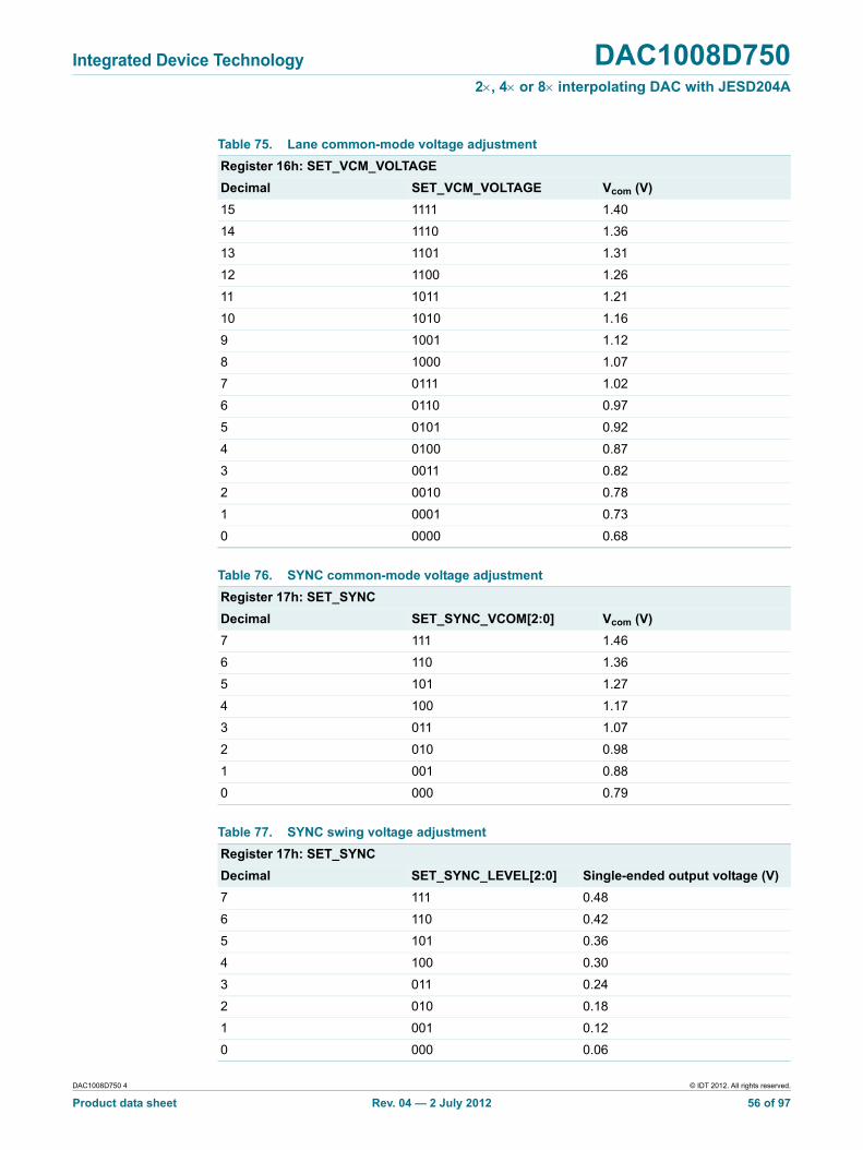
Integrated Device Technology DAC1008D7502, 4 or 8 interpolating DAC with JESD204A
Table 75. Lane common-mode voltage adjustment
Register 16h: SET_VCM_VOLTAGE
Decimal SET_VCM_VOLTAGE Vcom (V)
15 1111 1.40
14 1110 1.36
13 1101 1.31
12 1100 1.26
11 1011 1.21
10 1010 1.16
9 1001 1.12
8 1000 1.07
7 0111 1.02
6 0110 0.97
5 0101 0.92
4 0100 0.87
3 0011 0.82
2 0010 0.78
1 0001 0.73
0 0000 0.68
Table 76. SYNC common-mode voltage adjustment
Register 17h: SET_SYNC
Decimal SET_SYNC_VCOM[2:0] Vcom (V)
7 111 1.46
6 110 1.36
5 101 1.27
4 100 1.17
3 011 1.07
2 010 0.98
1 001 0.88
0 000 0.79
Table 77. SYNC swing voltage adjustment
Register 17h: SET_SYNC
Decimal SET_SYNC_LEVEL[2:0] Single-ended output voltage (V)
7 111 0.48
6 110 0.42
5 101 0.36
4 100 0.30
3 011 0.24
2 010 0.18
1 001 0.12
0 000 0.06
DAC1008D750 4 © IDT 2012. All rights reserved.
Product data sheet Rev. 04 — 2 July 2012 56 of 97
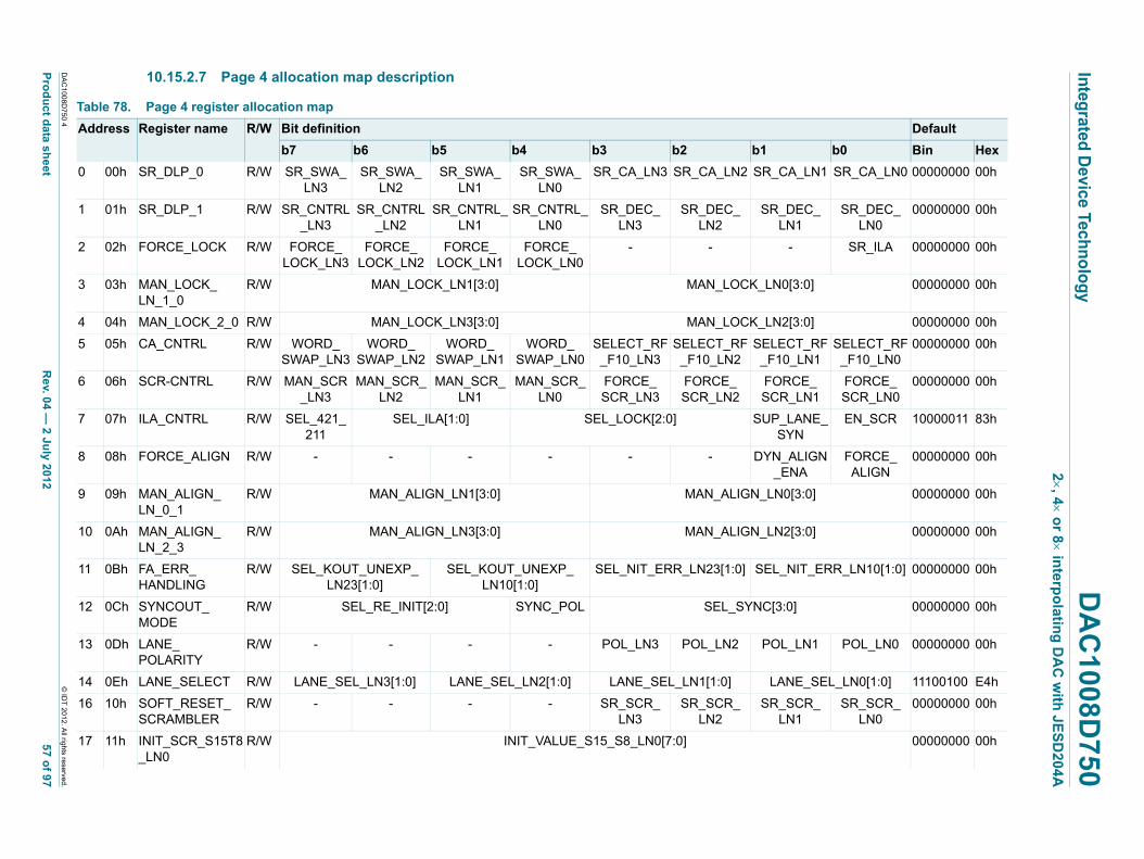
xxxxxxxxxxxxxxxxxxxxx xxxxxxxxxxxxxxxxxxxxxxxxxx xxxxxxx x x x xxxxxxxxxxxxxxxxxxxxxxxxxxxxxx xxxxxxxxxxxxxxxxxxx xx xx xxxxx xxxxxxxxxxxxxxxxxxxxxxxxxxx xxxxxxxxxxxxxxxxxxx xxxxxx xxxxxxxxxxxxxxxxxxxxxxxxxxxxxxxxxxx xxxxxxxxxxxx x x xxxxxxxxxxxxxxxxxxxxx xxxxxxxxxxxxxxxxxxxxxxxxxxxxxx xxxxx xxxxxxxxxxxxxxxxxxxxxxxxxxxxxxxxxxxxxxxxxxxxxxxxxx xxxxxxxx xxxxxxxxxxxxxxxxxxxxxxxxx xxxxxxxxxxxxxxxxxxxx xxx
DA
C100
8D750
4
Pro
du
ct data sh
eetR
ev. 04 —
2 July 2012
57 o
f 97
Integ
rated D
evice Techn
olo
gy
DA
C1008D
7502, 4 o
r 8 inte
rpo
lating
DA
C w
ith J
ES
D20
4A10.15.2.7 Page 4 allocation map description
Table 78. Page 4 register allocation map
Default
b0 Bin Hex
LN1 SR_CA_LN0 00000000 00h
C_ SR_DEC_LN0
00000000 00h
SR_ILA 00000000 00h
:0] 00000000 00h
:0] 00000000 00h
_RFN1
SELECT_RF_F10_LN0
00000000 00h
E_N1
FORCE_SCR_LN0
00000000 00h
NE_ EN_SCR 10000011 83h
IGN FORCE_ALIGN
00000000 00h
:0] 00000000 00h
:0] 00000000 00h
_ERR_LN10[1:0] 00000000 00h
00000000 00h
N1 POL_LN0 00000000 00h
_SEL_LN0[1:0] 11100100 E4h
R_ SR_SCR_LN0
00000000 00h
00000000 00h
© ID
T 20
12. All rights reserved
.
Address Register name R/W Bit definition
b7 b6 b5 b4 b3 b2 b1
0 00h SR_DLP_0 R/W SR_SWA_LN3
SR_SWA_LN2
SR_SWA_LN1
SR_SWA_LN0
SR_CA_LN3 SR_CA_LN2 SR_CA_
1 01h SR_DLP_1 R/W SR_CNTRL_LN3
SR_CNTRL_LN2
SR_CNTRL_LN1
SR_CNTRL_LN0
SR_DEC_LN3
SR_DEC_LN2
SR_DELN1
2 02h FORCE_LOCK R/W FORCE_LOCK_LN3
FORCE_LOCK_LN2
FORCE_LOCK_LN1
FORCE_LOCK_LN0
- - -
3 03h MAN_LOCK_LN_1_0
R/W MAN_LOCK_LN1[3:0] MAN_LOCK_LN0[3
4 04h MAN_LOCK_2_0 R/W MAN_LOCK_LN3[3:0] MAN_LOCK_LN2[3
5 05h CA_CNTRL R/W WORD_SWAP_LN3
WORD_SWAP_LN2
WORD_SWAP_LN1
WORD_SWAP_LN0
SELECT_RF_F10_LN3
SELECT_RF_F10_LN2
SELECT_F10_L
6 06h SCR-CNTRL R/W MAN_SCR_LN3
MAN_SCR_LN2
MAN_SCR_LN1
MAN_SCR_LN0
FORCE_SCR_LN3
FORCE_SCR_LN2
FORCSCR_L
7 07h ILA_CNTRL R/W SEL_421_211
SEL_ILA[1:0] SEL_LOCK[2:0] SUP_LASYN
8 08h FORCE_ALIGN R/W - - - - - - DYN_AL_ENA
9 09h MAN_ALIGN_LN_0_1
R/W MAN_ALIGN_LN1[3:0] MAN_ALIGN_LN0[3
10 0Ah MAN_ALIGN_LN_2_3
R/W MAN_ALIGN_LN3[3:0] MAN_ALIGN_LN2[3
11 0Bh FA_ERR_HANDLING
R/W SEL_KOUT_UNEXP_LN23[1:0]
SEL_KOUT_UNEXP_LN10[1:0]
SEL_NIT_ERR_LN23[1:0] SEL_NIT
12 0Ch SYNCOUT_MODE
R/W SEL_RE_INIT[2:0] SYNC_POL SEL_SYNC[3:0]
13 0Dh LANE_POLARITY
R/W - - - - POL_LN3 POL_LN2 POL_L
14 0Eh LANE_SELECT R/W LANE_SEL_LN3[1:0] LANE_SEL_LN2[1:0] LANE_SEL_LN1[1:0] LANE
16 10h SOFT_RESET_SCRAMBLER
R/W - - - - SR_SCR_LN3
SR_SCR_LN2
SR_SCLN1
17 11h INIT_SCR_S15T8_LN0
R/W INIT_VALUE_S15_S8_LN0[7:0]
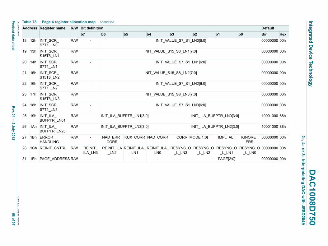
xxxxxxxxxxxxxxxxxxxxx xxxxxxxxxxxxxxxxxxxxxxxxxx xxxxxxx x x x xxxxxxxxxxxxxxxxxxxxxxxxxxxxxx xxxxxxxxxxxxxxxxxxx xx xx xxxxx xxxxxxxxxxxxxxxxxxxxxxxxxxx xxxxxxxxxxxxxxxxxxx xxxxxx xxxxxxxxxxxxxxxxxxxxxxxxxxxxxxxxxxx xxxxxxxxxxxx x x xxxxxxxxxxxxxxxxxxxxx xxxxxxxxxxxxxxxxxxxxxxxxxxxxxx xxxxx xxxxxxxxxxxxxxxxxxxxxxxxxxxxxxxxxxxxxxxxxxxxxxxxxx xxxxxxxx xxxxxxxxxxxxxxxxxxxxxxxxx xxxxxxxxxxxxxxxxxxxx xxx
DA
C100
8D750
4
Pro
du
ct data sh
eetR
ev. 04 —
2 July 2012
58 o
f 97
Integ
rated D
evice Techn
olo
gy
DA
C1008D
7502, 4 o
r 8 inte
rpo
lating
DA
C w
ith J
ES
D20
4A
00000000 00h
00000000 00h
00000000 00h
00000000 00h
00000000 00h
00000000 00h
00000000 00h
0[3:0] 10001000 88h
2[3:0] 10001000 88h
LT IGNORE_ERR
00000000 00h
_O1
RESYNC_O_L_LN0
00000000 00h
:0] 00000000 00h
Table 78. Page 4 register allocation map …continued
Address Register name R/W Bit definition Default
b7 b6 b5 b4 b3 b2 b1 b0 Bin Hex
© ID
T 20
12. All rights reserved
.
18 12h INIT_SCR_S7T1_LN0
R/W - INIT_VALUE_S7_S1_LN0[6:0]
19 13h INIT_SCR_S15T8_LN1
R/W INIT_VALUE_S15_S8_LN1[7:0]
20 14h INIT_SCR_S7T1_LN1
R/W - INIT_VALUE_S7_S1_LN1[6:0]
21 15h INIT_SCR_S15T8_LN2
R/W INIT_VALUE_S15_S8_LN2[7:0]
22 16h INIT_SCR_S7T1_LN2
R/W - INIT_VALUE_S7_S1_LN2[6:0]
23 17h INIT_SCR_S15T8_LN3
R/W INIT_VALUE_S15_S8_LN3[7:0]
24 18h INIT_SCR_S7T1_LN3
R/W - INIT_VALUE_S7_S1_LN3[6:0]
25 19h INIT_ILA_BUFPTR_LN01
R/W INIT_ILA_BUFPTR_LN1[3:0] INIT_ILA_BUFPTR_LN
26 1Ah INIT_ILA_BUFPTR_LN23
R/W INIT_ILA_BUFPTR_LN3[3:0] INIT_ILA_BUFPTR_LN
27 1Bh ERROR_HANDLING
R/W - NAD_ERR_CORR
KUX_CORR NAD_CORR CORR_MODE[1:0] IMPL_A
28 1Ch REINIT_CNTRL R/W REINIT_ILA_LN3
REINIT_ILA_LN2
REINIT_ILA_LN1
REINIT_ILA_LN0
RESYNC_O_L_LN3
RESYNC_O_L_LN2
RESYNC_L_LN
31 1Fh PAGE_ADDRESS R/W - - - - - PAGE[2
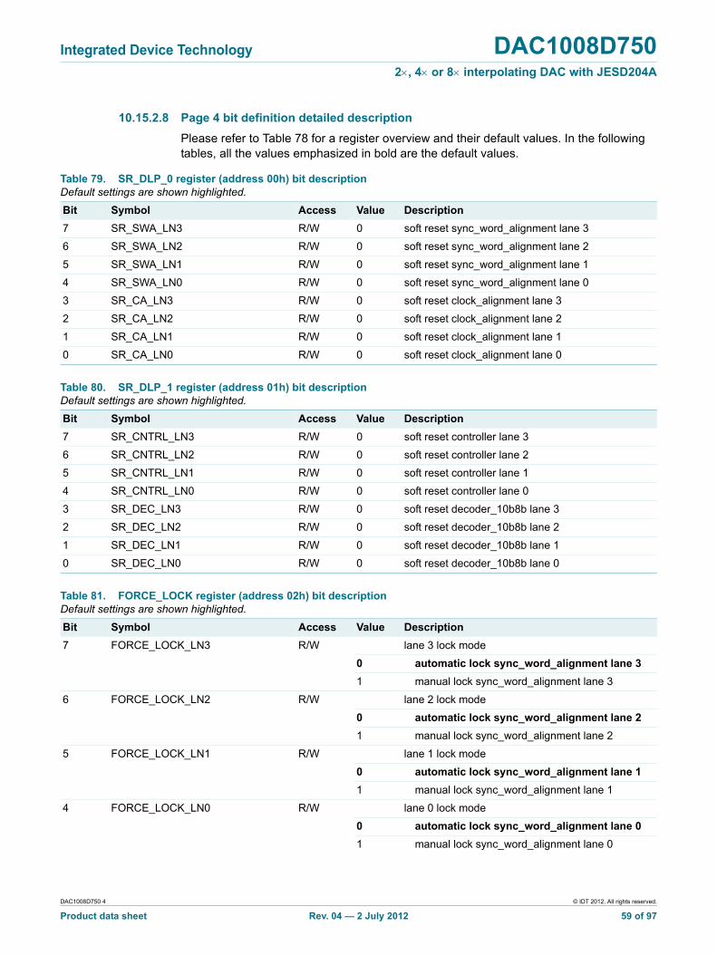
Integrated Device Technology DAC1008D7502, 4 or 8 interpolating DAC with JESD204A
10.15.2.8 Page 4 bit definition detailed description
Please refer to Table 78 for a register overview and their default values. In the following tables, all the values emphasized in bold are the default values.
Table 79. SR_DLP_0 register (address 00h) bit descriptionDefault settings are shown highlighted.
Bit Symbol Access Value Description
7 SR_SWA_LN3 R/W 0 soft reset sync_word_alignment lane 3
6 SR_SWA_LN2 R/W 0 soft reset sync_word_alignment lane 2
5 SR_SWA_LN1 R/W 0 soft reset sync_word_alignment lane 1
4 SR_SWA_LN0 R/W 0 soft reset sync_word_alignment lane 0
3 SR_CA_LN3 R/W 0 soft reset clock_alignment lane 3
2 SR_CA_LN2 R/W 0 soft reset clock_alignment lane 2
1 SR_CA_LN1 R/W 0 soft reset clock_alignment lane 1
0 SR_CA_LN0 R/W 0 soft reset clock_alignment lane 0
Table 80. SR_DLP_1 register (address 01h) bit descriptionDefault settings are shown highlighted.
Bit Symbol Access Value Description
7 SR_CNTRL_LN3 R/W 0 soft reset controller lane 3
6 SR_CNTRL_LN2 R/W 0 soft reset controller lane 2
5 SR_CNTRL_LN1 R/W 0 soft reset controller lane 1
4 SR_CNTRL_LN0 R/W 0 soft reset controller lane 0
3 SR_DEC_LN3 R/W 0 soft reset decoder_10b8b lane 3
2 SR_DEC_LN2 R/W 0 soft reset decoder_10b8b lane 2
1 SR_DEC_LN1 R/W 0 soft reset decoder_10b8b lane 1
0 SR_DEC_LN0 R/W 0 soft reset decoder_10b8b lane 0
Table 81. FORCE_LOCK register (address 02h) bit descriptionDefault settings are shown highlighted.
Bit Symbol Access Value Description
7 FORCE_LOCK_LN3 R/W lane 3 lock mode
0 automatic lock sync_word_alignment lane 3
1 manual lock sync_word_alignment lane 3
6 FORCE_LOCK_LN2 R/W lane 2 lock mode
0 automatic lock sync_word_alignment lane 2
1 manual lock sync_word_alignment lane 2
5 FORCE_LOCK_LN1 R/W lane 1 lock mode
0 automatic lock sync_word_alignment lane 1
1 manual lock sync_word_alignment lane 1
4 FORCE_LOCK_LN0 R/W lane 0 lock mode
0 automatic lock sync_word_alignment lane 0
1 manual lock sync_word_alignment lane 0
DAC1008D750 4 © IDT 2012. All rights reserved.
Product data sheet Rev. 04 — 2 July 2012 59 of 97

Integrated Device Technology DAC1008D7502, 4 or 8 interpolating DAC with JESD204A
0 SR_ILA R/W soft reset inter-lane alignment
0 no action
1 reset
Table 81. FORCE_LOCK register (address 02h) bit description …continuedDefault settings are shown highlighted.
Bit Symbol Access Value Description
Table 82. MAN_LOCK_LN_1_0 register (address 03h) bit descriptionDefault settings are shown highlighted.
Bit Symbol Access Value Description
7 to 4 MAN_LOCK_LN1[3:0] R/W 0h manual lock setting synchronization word alignment lane 1
3 to 0 MAN_LOCK_LN0[3:0] R/W 0h manual lock setting synchronization word alignment lane 0
Table 83. MAN_LOCK_2_0 register (address 04h) bit descriptionDefault settings are shown highlighted.
Bit Symbol Access Value Description
7 to 4 MAN_LOCK_LN3[3:0] R/W 0h manual lock setting synchronization word alignment lane 3
3 to 0 MAN_LOCK_LN2[3:0] R/W 0h manual lock setting synchronization word alignment lane 2
Table 84. CA_CNTRL register (address 05h) bit description
Bit Symbol Access Value Description
7 WORD_SWAP_LN3 R/W lane 3 bit swapping
0 dout_ca_ln3[7:0] = din_ca_ln3[7:0]
1 dout_ca_ln3[7:0] = din_ca_ln3[0:7]
6 WORD_SWAP_LN2 R/W lane 2 bit swapping
0 dout_ca_ln2[7:0] = din_ca_ln2[7:0]
1 dout_ca_ln2[7:0] = din_ca_ln2[0:7]
5 WORD_SWAP_LN1 R/W lane 1 bit swapping
0 dout_ca_ln1[7:0] = din_ca_ln1[7:0]
1 dout_ca_ln1[7:0] = din_ca_ln1[0:7]
4 WORD_SWAP_LN0 R/W lane 0 bit swapping
0 dout_ca_ln0[7:0] = din_ca_ln0[7:0]
1 dout_ca_ln0[7:0] = din_ca_ln0[0:7]
3 SELECT_RF_F10_LN3 R/W lane 3 sampling mode
0 din_ca_ln3 sampled at falling edge f10_ln3
1 din_ca_ln3 sampled at rising edge f10_ln3
2 SELECT_RF_F10_LN2 R/W lane 2 sampling mode
0 din_ca_ln2 sampled at falling edge f10_ln2
1 din_ca_ln2 sampled at rising edge f10_ln2
DAC1008D750 4 © IDT 2012. All rights reserved.
Product data sheet Rev. 04 — 2 July 2012 60 of 97

Integrated Device Technology DAC1008D7502, 4 or 8 interpolating DAC with JESD204A
1 SELECT_RF_F10_LN1 R/W lane 1 sampling mode
0 din_ca_ln1 sampled at falling edge f10_ln1
1 din_ca_ln1 sampled at rising edge f10_ln1
0 SELECT_RF_F10_LN0 R/W lane 0 sampling mode
0 din_ca_ln0 sampled at falling edge f10_ln0
1 din_ca_ln0 sampled at rising edge f10_ln0
Table 84. CA_CNTRL register (address 05h) bit description …continued
Bit Symbol Access Value Description
Table 85. SCR_CNTRL register (address 06h) bit description
Bit Symbol Access Value Description
7 MAN_SCR_LN3 R/W lane 3 manual scrambling
0 scrambling lane 3 off (when force_scr_ln3 = 1)
1 scrambling lane 3 on (when force_scr_ln3 = 1)
6 MAN_SCR_LN2 R/W lane 2 manual scrambling
0 scrambling lane 2 off (when force_scr_ln2 = 1)
1 scrambling lane 2 on (when force_scr_ln2 = 1)
5 MAN_SCR_LN1 R/W lane 1 manual scrambling
0 scrambling lane 1 off (when force_scr_ln1 = 1)
1 scrambling lane 1 on (when force_scr_ln1 = 1)
4 MAN_SCR_LN0 R/W lane 0 manual scrambling
0 scrambling lane 0 off (when force_scr_ln0 = 1)
1 scrambling lane 0 on (when force_scr_ln0 = 1)
3 FORCE_SCR_LN3 R/W lane 3 scrambling mode
0 scrambling lane 3 depends on lock_ln3 and en_scr
1 scrambling lane 3 depends on man_scr_ln3
2 FORCE_SCR_LN2 R/W lane 2 scrambling mode
0 scrambling lane 2 depends on lock_ln2 and en_scr
1 scrambling lane 2 depends on man_scr_ln2
1 FORCE_SCR_LN1 R/W lane 1 scrambling mode
0 scrambling lane 1 depends on lock_ln1 and en_scr
1 scrambling lane 1 depends on man_scr_ln1
0 FORCE_SCR_LN0 R/W lane 0 scrambling mode
0 scrambling lane 0 depends on lock_ln0 and en_scr
1 scrambling lane 0 depends on man_scr_ln0
DAC1008D750 4 © IDT 2012. All rights reserved.
Product data sheet Rev. 04 — 2 July 2012 61 of 97

Integrated Device Technology DAC1008D7502, 4 or 8 interpolating DAC with JESD204A
Table 86. ILA_CNTRL register (address 07h) bit description
Bit Symbol Access Value Description
7 SEL_421_211 R/W inter-lane alignment mode
0 inter-lane alignment based on lane 3 : lane 2 and/or lane 1 : lane 0
1 inter-lane alignment based on ln3 : ln0
6 to 5 SEL_ILA[1:0] R/W inter-lane alignment trigger mode
00 inter-lane alignment is done after receiving 1 /A/-symbol
01 inter-lane alignment is done after receiving 2 /A/-symbols
10 inter-lane alignment is done after receiving 3 /A/-symbols
11 inter-lane alignment is done after receiving 4 /A/-symbols
4 to 2 SEL_LOCK[2:0] R/W inter-lane alignment start mode
000 inter-lane alignment may start only if all (4 or 2) lanes are locked
001 inter-lane alignment may start if one of the (4 or 2) lanes are locked
010 inter-lane alignment may start if lane 0 is locked
011 inter-lane alignment may start if lane 1 is locked
100 inter-lane alignment may start if lane 2 is locked
101 inter-lane alignment may start if lane 3 is locked
1 SUP_LANE_SYN R/W inter-lane alignment enable
0 inter-lane alignment synchronization disabled
1 inter-lane alignment synchronization enabled
0 EN_SCR R/W data descrambling
0 disabled
1 enabled
Table 87. FORCE_ALIGN register (address 08h) bit description
Bit Symbol Access Value Description
1 DYN_ALIGN_ENA R/W dynamic re-alignment mode
0 no dynamic re-alignment
1 dynamic re-alignment (and monitoring) enabled
0 FORCE_ALIGN R/W lane alignment mode
0 automatic lane alignment based on /A/ symbols
1 manual lane alignment based on man_align_lnx
Table 88. MAN_ALIGN_LN_0_1 register (address 09h) bit description
Bit Symbol Access Value Description
7 to 4 MAN_ALIGN_LN1[3:0] R/W 0h indicates alignment data-delay for lane 1 [1..15]
3 to 0 MAN_ALIGN_LN0[3:0] R/W 0h indicates alignment data-delay for lane 0 [1..15]
DAC1008D750 4 © IDT 2012. All rights reserved.
Product data sheet Rev. 04 — 2 July 2012 62 of 97
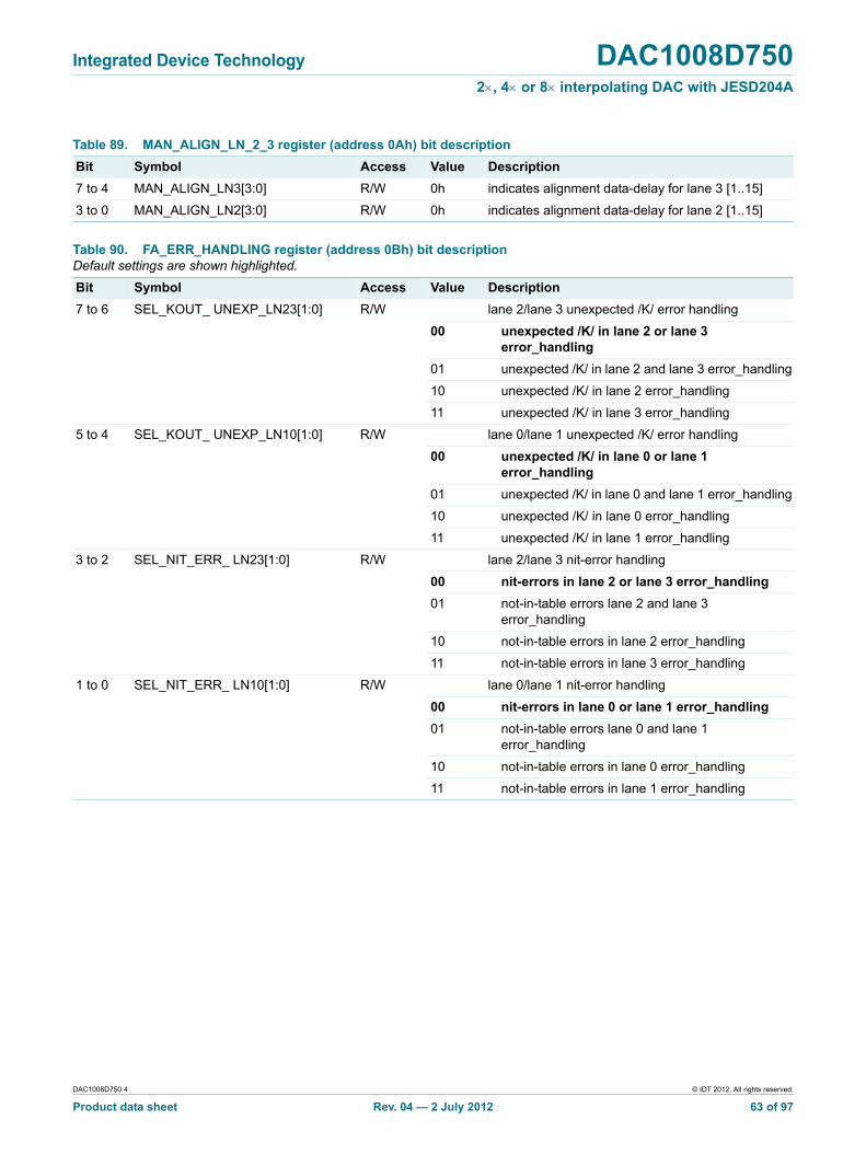
Integrated Device Technology DAC1008D7502, 4 or 8 interpolating DAC with JESD204A
Table 89. MAN_ALIGN_LN_2_3 register (address 0Ah) bit description
Bit Symbol Access Value Description
7 to 4 MAN_ALIGN_LN3[3:0] R/W 0h indicates alignment data-delay for lane 3 [1..15]
3 to 0 MAN_ALIGN_LN2[3:0] R/W 0h indicates alignment data-delay for lane 2 [1..15]
Table 90. FA_ERR_HANDLING register (address 0Bh) bit descriptionDefault settings are shown highlighted.
Bit Symbol Access Value Description
7 to 6 SEL_KOUT_ UNEXP_LN23[1:0] R/W lane 2/lane 3 unexpected /K/ error handling
00 unexpected /K/ in lane 2 or lane 3 error_handling
01 unexpected /K/ in lane 2 and lane 3 error_handling
10 unexpected /K/ in lane 2 error_handling
11 unexpected /K/ in lane 3 error_handling
5 to 4 SEL_KOUT_ UNEXP_LN10[1:0] R/W lane 0/lane 1 unexpected /K/ error handling
00 unexpected /K/ in lane 0 or lane 1 error_handling
01 unexpected /K/ in lane 0 and lane 1 error_handling
10 unexpected /K/ in lane 0 error_handling
11 unexpected /K/ in lane 1 error_handling
3 to 2 SEL_NIT_ERR_ LN23[1:0] R/W lane 2/lane 3 nit-error handling
00 nit-errors in lane 2 or lane 3 error_handling
01 not-in-table errors lane 2 and lane 3 error_handling
10 not-in-table errors in lane 2 error_handling
11 not-in-table errors in lane 3 error_handling
1 to 0 SEL_NIT_ERR_ LN10[1:0] R/W lane 0/lane 1 nit-error handling
00 nit-errors in lane 0 or lane 1 error_handling
01 not-in-table errors lane 0 and lane 1 error_handling
10 not-in-table errors in lane 0 error_handling
11 not-in-table errors in lane 1 error_handling
DAC1008D750 4 © IDT 2012. All rights reserved.
Product data sheet Rev. 04 — 2 July 2012 63 of 97

Integrated Device Technology DAC1008D7502, 4 or 8 interpolating DAC with JESD204A
Table 91. SYNCOUT_MODE register (address 0Ch) bit descriptionDefault settings are shown highlighted.
Bit Symbol Access Value Description
7 to 5 SEL_RE_INIT[2:0] R/W reinitialization mode
000 i_re_init when 1 of the lane_rst's is active
001 i_re_init when rst_ln0 or rst_ln1 is active
010 i_re_init when rst_ln2 or rst_ln3 is active
011 i_re_init when rst_ln0 is active
100 i_re_init when rst_ln1 is active
101 i_re_init when rst_ln2 is active
110 i_re_init when rst_ln3 is active
111 i_re_init remains '0'
4 SYNC_POL R/W synchronization polarity
0 sync_out is active when LOW
1 sync_out is active when HIGH
3 to 0 SEL_SYNC[3:0] R/W synchronization mode
0000 sync when one of the four lane_syncs is active
0001 sync when all four lane_syncs are active
0010 sync when sync_ln0 or sync_ln1 is active
0011 sync when both sync_ln0 and sync_ln1 are active
0100 sync when sync_ln2 or sync_ln3 is active
0101 sync when both sync_ln2 and sync_ln3 are active
0110 sync when sync_ln0 is active
0111 sync when sync_ln1 is active
1000 sync when sync_ln2 is active
1001 sync when sync_ln3 is active
1010 sync remains fixed '1'
other sync remains fixed '0'
Table 92. LANE_POLARITY register (address 0Dh) bit description
Bit Symbol Access Value Description
3 POL_LN3 R/W lane 3 data polarity
0 no action
1 invert all data bits of lane 3
2 POL_LN2 R/W lane 2 data polarity
0 no action
1 invert all data bits of lane 2
1 POL_LN1 R/W lane 1 data polarity
0 no action
1 invert all data bits of lane 1
0 POL_LN0 R/W lane 0 data polarity
0 no action
1 invert all data bits of lane 0
DAC1008D750 4 © IDT 2012. All rights reserved.
Product data sheet Rev. 04 — 2 July 2012 64 of 97
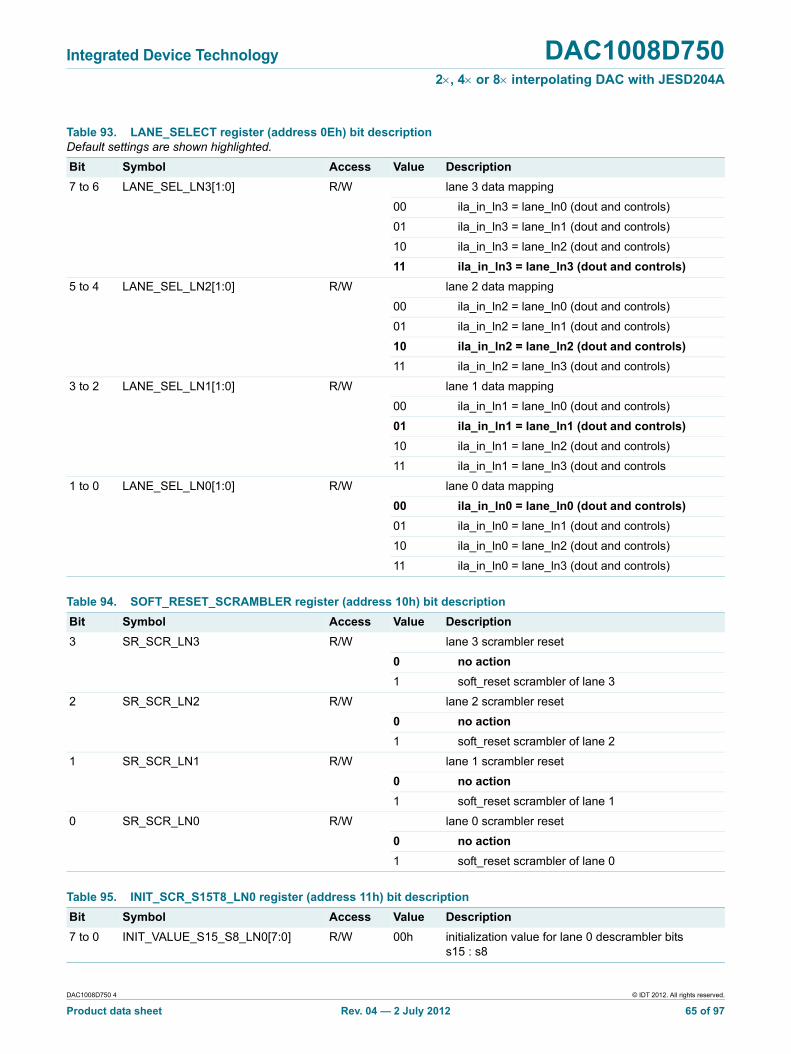
Integrated Device Technology DAC1008D7502, 4 or 8 interpolating DAC with JESD204A
Table 93. LANE_SELECT register (address 0Eh) bit descriptionDefault settings are shown highlighted.
Bit Symbol Access Value Description
7 to 6 LANE_SEL_LN3[1:0] R/W lane 3 data mapping
00 ila_in_ln3 = lane_ln0 (dout and controls)
01 ila_in_ln3 = lane_ln1 (dout and controls)
10 ila_in_ln3 = lane_ln2 (dout and controls)
11 ila_in_ln3 = lane_ln3 (dout and controls)
5 to 4 LANE_SEL_LN2[1:0] R/W lane 2 data mapping
00 ila_in_ln2 = lane_ln0 (dout and controls)
01 ila_in_ln2 = lane_ln1 (dout and controls)
10 ila_in_ln2 = lane_ln2 (dout and controls)
11 ila_in_ln2 = lane_ln3 (dout and controls)
3 to 2 LANE_SEL_LN1[1:0] R/W lane 1 data mapping
00 ila_in_ln1 = lane_ln0 (dout and controls)
01 ila_in_ln1 = lane_ln1 (dout and controls)
10 ila_in_ln1 = lane_ln2 (dout and controls)
11 ila_in_ln1 = lane_ln3 (dout and controls
1 to 0 LANE_SEL_LN0[1:0] R/W lane 0 data mapping
00 ila_in_ln0 = lane_ln0 (dout and controls)
01 ila_in_ln0 = lane_ln1 (dout and controls)
10 ila_in_ln0 = lane_ln2 (dout and controls)
11 ila_in_ln0 = lane_ln3 (dout and controls)
Table 94. SOFT_RESET_SCRAMBLER register (address 10h) bit description
Bit Symbol Access Value Description
3 SR_SCR_LN3 R/W lane 3 scrambler reset
0 no action
1 soft_reset scrambler of lane 3
2 SR_SCR_LN2 R/W lane 2 scrambler reset
0 no action
1 soft_reset scrambler of lane 2
1 SR_SCR_LN1 R/W lane 1 scrambler reset
0 no action
1 soft_reset scrambler of lane 1
0 SR_SCR_LN0 R/W lane 0 scrambler reset
0 no action
1 soft_reset scrambler of lane 0
Table 95. INIT_SCR_S15T8_LN0 register (address 11h) bit description
Bit Symbol Access Value Description
7 to 0 INIT_VALUE_S15_S8_LN0[7:0] R/W 00h initialization value for lane 0 descrambler bits s15 : s8
DAC1008D750 4 © IDT 2012. All rights reserved.
Product data sheet Rev. 04 — 2 July 2012 65 of 97
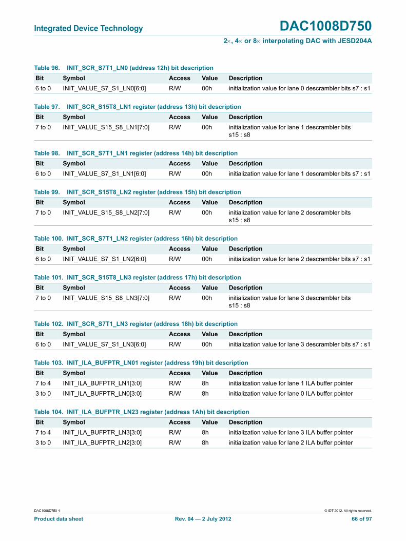
Integrated Device Technology DAC1008D7502, 4 or 8 interpolating DAC with JESD204A
Table 96. INIT_SCR_S7T1_LN0 (address 12h) bit description
Bit Symbol Access Value Description
6 to 0 INIT_VALUE_S7_S1_LN0[6:0] R/W 00h initialization value for lane 0 descrambler bits s7 : s1
Table 97. INIT_SCR_S15T8_LN1 register (address 13h) bit description
Bit Symbol Access Value Description
7 to 0 INIT_VALUE_S15_S8_LN1[7:0] R/W 00h initialization value for lane 1 descrambler bits s15 : s8
Table 98. INIT_SCR_S7T1_LN1 register (address 14h) bit description
Bit Symbol Access Value Description
6 to 0 INIT_VALUE_S7_S1_LN1[6:0] R/W 00h initialization value for lane 1 descrambler bits s7 : s1
Table 99. INIT_SCR_S15T8_LN2 register (address 15h) bit description
Bit Symbol Access Value Description
7 to 0 INIT_VALUE_S15_S8_LN2[7:0] R/W 00h initialization value for lane 2 descrambler bits s15 : s8
Table 100. INIT_SCR_S7T1_LN2 register (address 16h) bit description
Bit Symbol Access Value Description
6 to 0 INIT_VALUE_S7_S1_LN2[6:0] R/W 00h initialization value for lane 2 descrambler bits s7 : s1
Table 101. INIT_SCR_S15T8_LN3 register (address 17h) bit description
Bit Symbol Access Value Description
7 to 0 INIT_VALUE_S15_S8_LN3[7:0] R/W 00h initialization value for lane 3 descrambler bits s15 : s8
Table 102. INIT_SCR_S7T1_LN3 register (address 18h) bit description
Bit Symbol Access Value Description
6 to 0 INIT_VALUE_S7_S1_LN3[6:0] R/W 00h initialization value for lane 3 descrambler bits s7 : s1
Table 103. INIT_ILA_BUFPTR_LN01 register (address 19h) bit description
Bit Symbol Access Value Description
7 to 4 INIT_ILA_BUFPTR_LN1[3:0] R/W 8h initialization value for lane 1 ILA buffer pointer
3 to 0 INIT_ILA_BUFPTR_LN0[3:0] R/W 8h initialization value for lane 0 ILA buffer pointer
Table 104. INIT_ILA_BUFPTR_LN23 register (address 1Ah) bit description
Bit Symbol Access Value Description
7 to 4 INIT_ILA_BUFPTR_LN3[3:0] R/W 8h initialization value for lane 3 ILA buffer pointer
3 to 0 INIT_ILA_BUFPTR_LN2[3:0] R/W 8h initialization value for lane 2 ILA buffer pointer
DAC1008D750 4 © IDT 2012. All rights reserved.
Product data sheet Rev. 04 — 2 July 2012 66 of 97
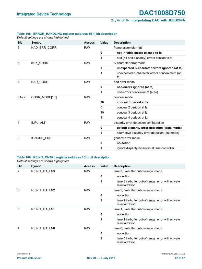
Integrated Device Technology DAC1008D7502, 4 or 8 interpolating DAC with JESD204A
Table 105. ERROR_HANDLING register (address 1Bh) bit descriptionDefault settings are shown highlighted.
Bit Symbol Access Value Description
6 NAD_ERR_CORR R/W frame assembler (fa)
0 not-in-table errors passed to fa
1 nad (nit and disparity) errors passed to fa
5 KUX_CORR R/W K-character error mode
0 unexpected K-character errors ignored (at fa)
1 unexpected K-character errors concealment (at fa)
4 NAD_CORR R/W nad error mode
0 nad-errors ignored (at fa)
1 nad-errors concealment (at fa)
3 to 2 CORR_MODE[1:0] R/W conceal mode
00 conceal 1 period at fa
01 conceal 2 periods at fa
10 conceal 3 periods at fa
11 conceal 4 periods at fa
1 IMPL_ALT R/W disparity error detection configuration
0 default disparity error detection (table mode)
1 alternative disparity error detection (cnt mode)
0 IGNORE_ERR R/W general error mode
0 no action
1 ignore disparity/nit-errors at lane-controller
Table 106. REINIT_CNTRL register (address 1Ch) bit descriptionDefault settings are shown highlighted.
Bit Symbol Access Value Description
7 REINIT_ILA_LN3 R/W lane 3, ila-buffer out-of-range check
0 no action
1 lane 3 ila-buffer out-of-range_error will activate reinitialization
6 REINIT_ILA_LN2 R/W lane 2, ila-buffer out-of-range check
0 no action
1 lane 2 ila-buffer out-of-range_error will activate reinitialization
5 REINIT_ILA_LN1 R/W lane 1, ila-buffer out-of-range check
0 no action
1 lane 1 ila-buffer out-of-range_error will activate reinitialization
4 REINIT_ILA_LN0 R/W lane 0, ila-buffer out-of-range check
0 no action
1 lane 0 ila-buffer out-of-range_error will activate reinitialization
DAC1008D750 4 © IDT 2012. All rights reserved.
Product data sheet Rev. 04 — 2 July 2012 67 of 97
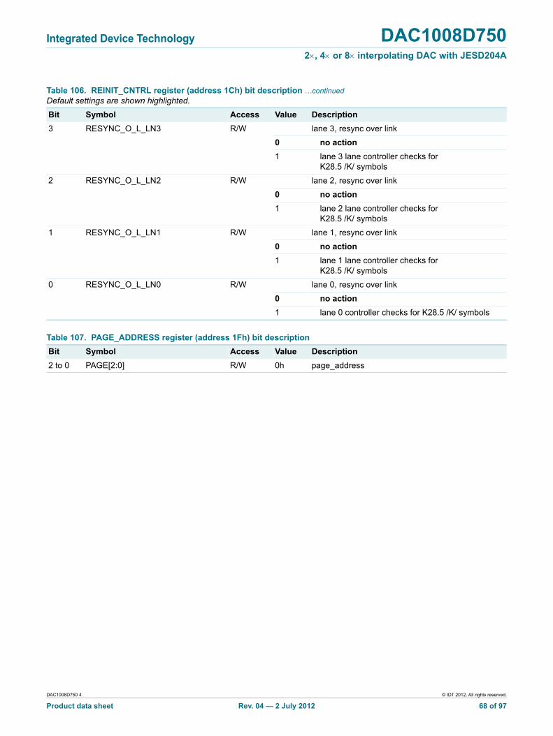
Integrated Device Technology DAC1008D7502, 4 or 8 interpolating DAC with JESD204A
3 RESYNC_O_L_LN3 R/W lane 3, resync over link
0 no action
1 lane 3 lane controller checks for K28.5 /K/ symbols
2 RESYNC_O_L_LN2 R/W lane 2, resync over link
0 no action
1 lane 2 lane controller checks for K28.5 /K/ symbols
1 RESYNC_O_L_LN1 R/W lane 1, resync over link
0 no action
1 lane 1 lane controller checks for K28.5 /K/ symbols
0 RESYNC_O_L_LN0 R/W lane 0, resync over link
0 no action
1 lane 0 controller checks for K28.5 /K/ symbols
Table 106. REINIT_CNTRL register (address 1Ch) bit description …continuedDefault settings are shown highlighted.
Bit Symbol Access Value Description
Table 107. PAGE_ADDRESS register (address 1Fh) bit description
Bit Symbol Access Value Description
2 to 0 PAGE[2:0] R/W 0h page_address
DAC1008D750 4 © IDT 2012. All rights reserved.
Product data sheet Rev. 04 — 2 July 2012 68 of 97
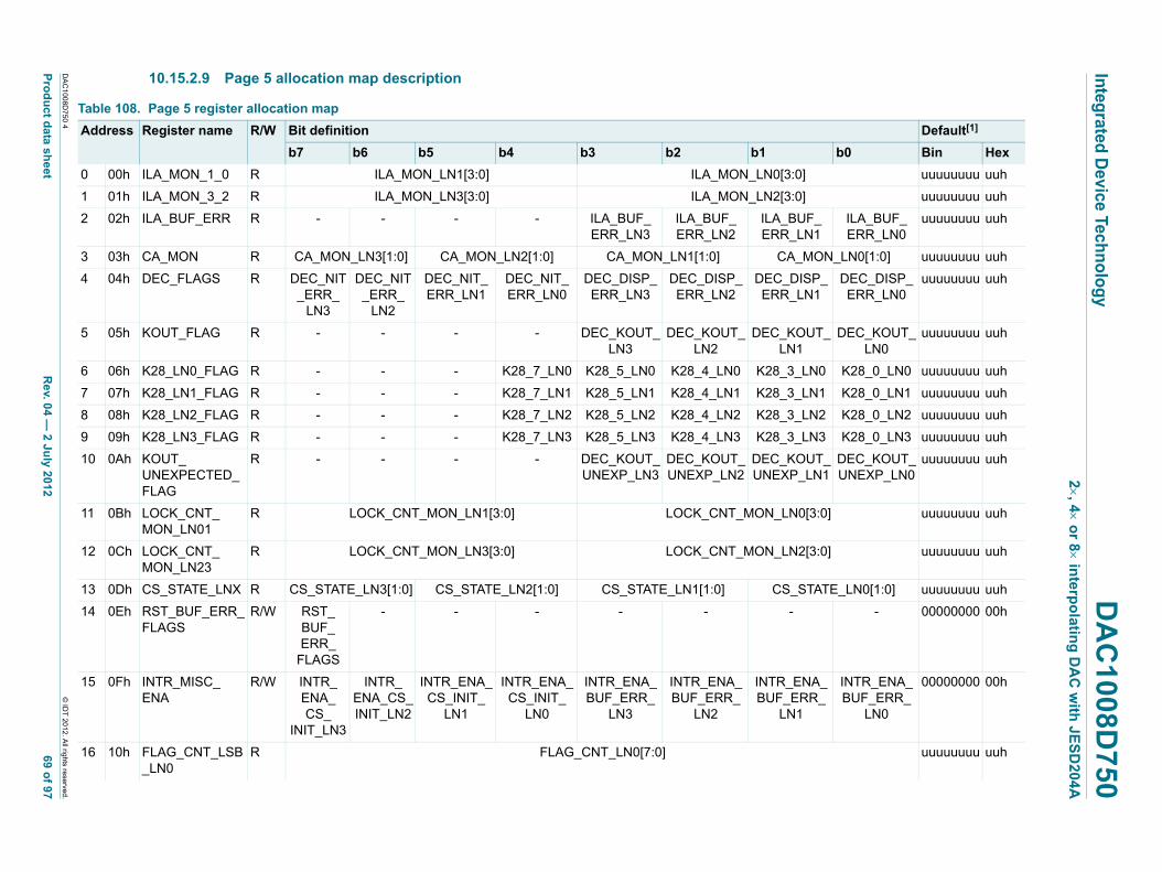
xxxxxxxxxxxxxxxxxxxxx xxxxxxxxxxxxxxxxxxxxxxxxxx xxxxxxx x x x xxxxxxxxxxxxxxxxxxxxxxxxxxxxxx xxxxxxxxxxxxxxxxxxx xx xx xxxxx xxxxxxxxxxxxxxxxxxxxxxxxxxx xxxxxxxxxxxxxxxxxxx xxxxxx xxxxxxxxxxxxxxxxxxxxxxxxxxxxxxxxxxx xxxxxxxxxxxx x x xxxxxxxxxxxxxxxxxxxxx xxxxxxxxxxxxxxxxxxxxxxxxxxxxxx xxxxx xxxxxxxxxxxxxxxxxxxxxxxxxxxxxxxxxxxxxxxxxxxxxxxxxx xxxxxxxx xxxxxxxxxxxxxxxxxxxxxxxxx xxxxxxxxxxxxxxxxxxxx xxx
DA
C100
8D750
4
Pro
du
ct data sh
eetR
ev. 04 —
2 July 2012
69 o
f 97
Integ
rated D
evice Techn
olo
gy
DA
C1008D
7502, 4 o
r 8 inte
rpo
lating
DA
C w
ith J
ES
D20
4A10.15.2.9 Page 5 allocation map description
Table 108. Page 5 register allocation map
Default[1]
b0 Bin Hex
uuuuuuuu uuh
uuuuuuuu uuh
_1
ILA_BUF_ERR_LN0
uuuuuuuu uuh
ON_LN0[1:0] uuuuuuuu uuh
_1
DEC_DISP_ERR_LN0
uuuuuuuu uuh
T_ DEC_KOUT_LN0
uuuuuuuu uuh
0 K28_0_LN0 uuuuuuuu uuh
1 K28_0_LN1 uuuuuuuu uuh
2 K28_0_LN2 uuuuuuuu uuh
3 K28_0_LN3 uuuuuuuu uuh
T_N1
DEC_KOUT_UNEXP_LN0
uuuuuuuu uuh
:0] uuuuuuuu uuh
:0] uuuuuuuu uuh
ATE_LN0[1:0] uuuuuuuu uuh
- 00000000 00h
__
INTR_ENA_BUF_ERR_
LN0
00000000 00h
uuuuuuuu uuh
© ID
T 20
12. All rights reserved
.
Address Register name R/W Bit definition
b7 b6 b5 b4 b3 b2 b1
0 00h ILA_MON_1_0 R ILA_MON_LN1[3:0] ILA_MON_LN0[3:0]
1 01h ILA_MON_3_2 R ILA_MON_LN3[3:0] ILA_MON_LN2[3:0]
2 02h ILA_BUF_ERR R - - - - ILA_BUF_ERR_LN3
ILA_BUF_ERR_LN2
ILA_BUFERR_LN
3 03h CA_MON R CA_MON_LN3[1:0] CA_MON_LN2[1:0] CA_MON_LN1[1:0] CA_M
4 04h DEC_FLAGS R DEC_NIT_ERR_
LN3
DEC_NIT_ERR_
LN2
DEC_NIT_ERR_LN1
DEC_NIT_ERR_LN0
DEC_DISP_ERR_LN3
DEC_DISP_ERR_LN2
DEC_DISPERR_LN
5 05h KOUT_FLAG R - - - - DEC_KOUT_LN3
DEC_KOUT_LN2
DEC_KOULN1
6 06h K28_LN0_FLAG R - - - K28_7_LN0 K28_5_LN0 K28_4_LN0 K28_3_LN
7 07h K28_LN1_FLAG R - - - K28_7_LN1 K28_5_LN1 K28_4_LN1 K28_3_LN
8 08h K28_LN2_FLAG R - - - K28_7_LN2 K28_5_LN2 K28_4_LN2 K28_3_LN
9 09h K28_LN3_FLAG R - - - K28_7_LN3 K28_5_LN3 K28_4_LN3 K28_3_LN
10 0Ah KOUT_UNEXPECTED_FLAG
R - - - - DEC_KOUT_UNEXP_LN3
DEC_KOUT_UNEXP_LN2
DEC_KOUUNEXP_L
11 0Bh LOCK_CNT_MON_LN01
R LOCK_CNT_MON_LN1[3:0] LOCK_CNT_MON_LN0[3
12 0Ch LOCK_CNT_MON_LN23
R LOCK_CNT_MON_LN3[3:0] LOCK_CNT_MON_LN2[3
13 0Dh CS_STATE_LNX R CS_STATE_LN3[1:0] CS_STATE_LN2[1:0] CS_STATE_LN1[1:0] CS_ST
14 0Eh RST_BUF_ERR_FLAGS
R/W RST_BUF_ERR_
FLAGS
- - - - - -
15 0Fh INTR_MISC_ENA
R/W INTR_ENA_CS_
INIT_LN3
INTR_ENA_CS_INIT_LN2
INTR_ENA_CS_INIT_
LN1
INTR_ENA_CS_INIT_
LN0
INTR_ENA_BUF_ERR_
LN3
INTR_ENA_BUF_ERR_
LN2
INTR_ENABUF_ERR
LN1
16 10h FLAG_CNT_LSB_LN0
R FLAG_CNT_LN0[7:0]
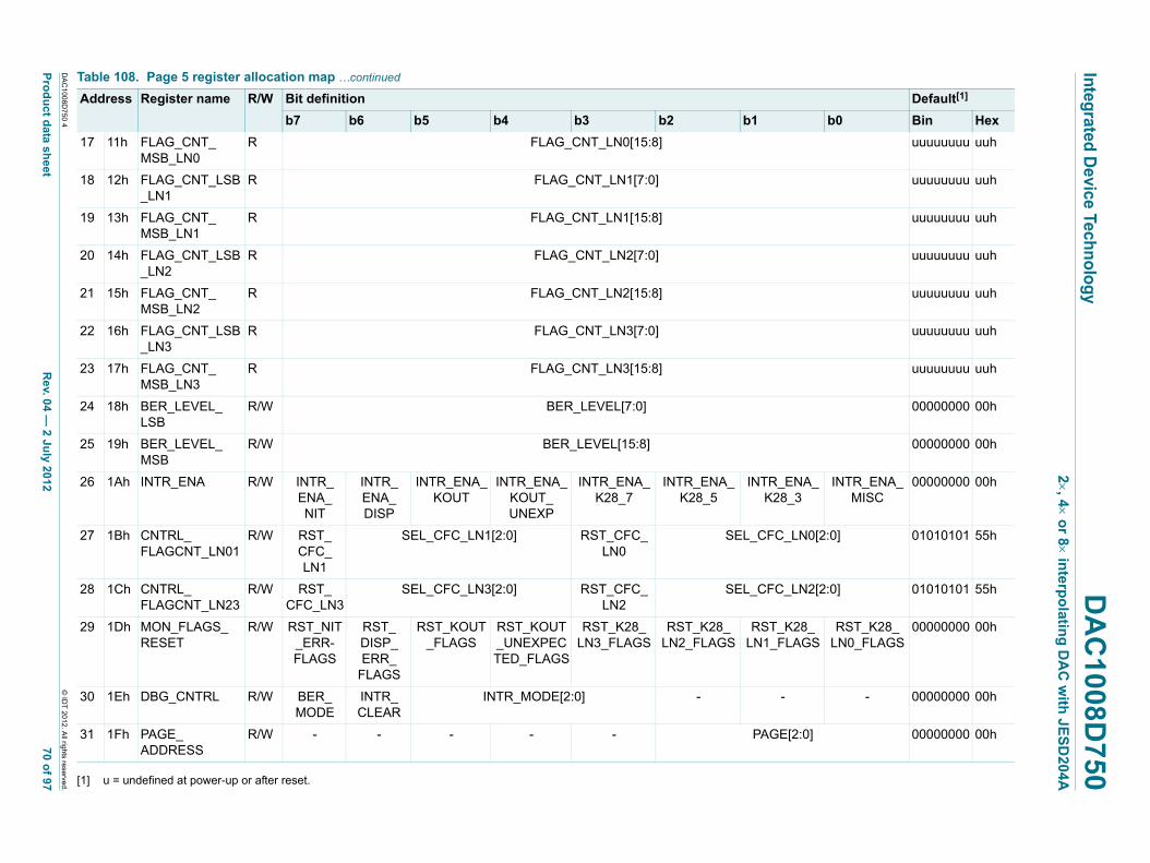
xxxxxxxxxxxxxxxxxxxxx xxxxxxxxxxxxxxxxxxxxxxxxxx xxxxxxx x x x xxxxxxxxxxxxxxxxxxxxxxxxxxxxxx xxxxxxxxxxxxxxxxxxx xx xx xxxxx xxxxxxxxxxxxxxxxxxxxxxxxxxx xxxxxxxxxxxxxxxxxxx xxxxxx xxxxxxxxxxxxxxxxxxxxxxxxxxxxxxxxxxx xxxxxxxxxxxx x x xxxxxxxxxxxxxxxxxxxxx xxxxxxxxxxxxxxxxxxxxxxxxxxxxxx xxxxx xxxxxxxxxxxxxxxxxxxxxxxxxxxxxxxxxxxxxxxxxxxxxxxxxx xxxxxxxx xxxxxxxxxxxxxxxxxxxxxxxxx xxxxxxxxxxxxxxxxxxxx xxx
DA
C100
8D750
4
Pro
du
ct data sh
eetR
ev. 04 —
2 July 2012
70 o
f 97
Integ
rated D
evice Techn
olo
gy
DA
C1008D
7502, 4 o
r 8 inte
rpo
lating
DA
C w
ith J
ES
D20
4A
uuuuuuuu uuh
uuuuuuuu uuh
uuuuuuuu uuh
uuuuuuuu uuh
uuuuuuuu uuh
uuuuuuuu uuh
uuuuuuuu uuh
00000000 00h
00000000 00h
_ INTR_ENA_MISC
00000000 00h
0[2:0] 01010101 55h
2[2:0] 01010101 55h
_S
RST_K28_LN0_FLAGS
00000000 00h
- 00000000 00h
] 00000000 00h
Table 108. Page 5 register allocation map …continued
Address Register name R/W Bit definition Default[1]
b7 b6 b5 b4 b3 b2 b1 b0 Bin Hex
© ID
T 20
12. All rights reserved
.
[1] u = undefined at power-up or after reset.
17 11h FLAG_CNT_MSB_LN0
R FLAG_CNT_LN0[15:8]
18 12h FLAG_CNT_LSB_LN1
R FLAG_CNT_LN1[7:0]
19 13h FLAG_CNT_MSB_LN1
R FLAG_CNT_LN1[15:8]
20 14h FLAG_CNT_LSB_LN2
R FLAG_CNT_LN2[7:0]
21 15h FLAG_CNT_MSB_LN2
R FLAG_CNT_LN2[15:8]
22 16h FLAG_CNT_LSB_LN3
R FLAG_CNT_LN3[7:0]
23 17h FLAG_CNT_MSB_LN3
R FLAG_CNT_LN3[15:8]
24 18h BER_LEVEL_LSB
R/W BER_LEVEL[7:0]
25 19h BER_LEVEL_MSB
R/W BER_LEVEL[15:8]
26 1Ah INTR_ENA R/W INTR_ENA_NIT
INTR_ENA_DISP
INTR_ENA_KOUT
INTR_ENA_KOUT_UNEXP
INTR_ENA_K28_7
INTR_ENA_K28_5
INTR_ENAK28_3
27 1Bh CNTRL_FLAGCNT_LN01
R/W RST_CFC_LN1
SEL_CFC_LN1[2:0] RST_CFC_LN0
SEL_CFC_LN
28 1Ch CNTRL_FLAGCNT_LN23
R/W RST_CFC_LN3
SEL_CFC_LN3[2:0] RST_CFC_LN2
SEL_CFC_LN
29 1Dh MON_FLAGS_RESET
R/W RST_NIT_ERR-FLAGS
RST_DISP_ERR_
FLAGS
RST_KOUT_FLAGS
RST_KOUT_UNEXPECTED_FLAGS
RST_K28_LN3_FLAGS
RST_K28_LN2_FLAGS
RST_K28LN1_FLAG
30 1Eh DBG_CNTRL R/W BER_MODE
INTR_CLEAR
INTR_MODE[2:0] - -
31 1Fh PAGE_ADDRESS
R/W - - - - - PAGE[2:0

Integrated Device Technology DAC1008D7502, 4 or 8 interpolating DAC with JESD204A
10.15.2.10 Page 5 bit definition detailed description
Please refer to Table 108 for a register overview and their default values. In the following tables, all the values emphasized in bold are the default values.
Table 109. ILA_MON_1_0 register (address 00h) bit descriptionDefault settings are shown highlighted.
Bit Symbol Access Value Description
7 to 4 ILA_MON_LN1[3:0] R - ila_buf_ln1 pointer
3 to 0 ILA_MON_LN0[3:0] R - ila_buf_ln0 pointer
Table 110. ILA_MON_3_2 register (address 01h) bit descriptionDefault settings are shown highlighted.
Bit Symbol Access Value Description
7 to 4 ILA_MON_LN3[3:0] R - ila_buf_ln3 pointer
3 to 0 ILA_MON_LN2[3:0] R - ila_buf_ln2 pointer
Table 111. ILA_BUF_ERR register (address 02h) bit descriptionDefault settings are shown highlighted.
Bit Symbol Access Value Description
3 ILA_BUF_ERR_LN3 R lane 3 ila buffer error
0 ila_buf_ln3 pointer is in range
1 ila_buf_ln3 pointer is out of range
2 ILA_BUF_ERR_LN2 R lane 2 ila buffer error
0 ila_buf_ln2 pointer is in range
1 ila_buf_ln2 pointer is out of range
1 ILA_BUF_ERR_LN1 R lane 1 ila buffer error
0 ila_buf_ln1 pointer is in range
1 ila_buf_ln1 pointer is out of range
0 ILA_BUF_ERR_LN0 R lane 0 ila buffer error
0 ila_buf_ln0 pointer is in range
1 ila_buf_ln0 pointer is out of range
Table 112. CA_MON register (address 03h) bit descriptionDefault settings are shown highlighted.
Bit Symbol Access Value Description
7 to 6 CA_MON_LN3[1:0] R - clock alignment phase monitor lane 3
5 to 4 CA_MON_LN2[1:0] R - clock alignment phase monitor lane 2
3 to 2 CA_MON_LN1[1:0] R - clock alignment phase monitor lane 1
1 to 0 CA_MON_LN0[1:0] R - clock alignment phase monitor lane 0
DAC1008D750 4 © IDT 2012. All rights reserved.
Product data sheet Rev. 04 — 2 July 2012 71 of 97
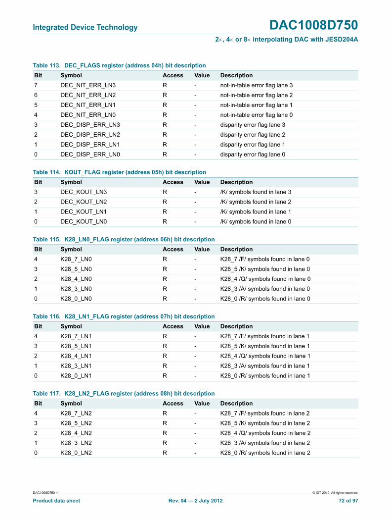
Integrated Device Technology DAC1008D7502, 4 or 8 interpolating DAC with JESD204A
Table 113. DEC_FLAGS register (address 04h) bit description
Bit Symbol Access Value Description
7 DEC_NIT_ERR_LN3 R - not-in-table error flag lane 3
6 DEC_NIT_ERR_LN2 R - not-in-table error flag lane 2
5 DEC_NIT_ERR_LN1 R - not-in-table error flag lane 1
4 DEC_NIT_ERR_LN0 R - not-in-table error flag lane 0
3 DEC_DISP_ERR_LN3 R - disparity error flag lane 3
2 DEC_DISP_ERR_LN2 R - disparity error flag lane 2
1 DEC_DISP_ERR_LN1 R - disparity error flag lane 1
0 DEC_DISP_ERR_LN0 R - disparity error flag lane 0
Table 114. KOUT_FLAG register (address 05h) bit description
Bit Symbol Access Value Description
3 DEC_KOUT_LN3 R - /K/ symbols found in lane 3
2 DEC_KOUT_LN2 R - /K/ symbols found in lane 2
1 DEC_KOUT_LN1 R - /K/ symbols found in lane 1
0 DEC_KOUT_LN0 R - /K/ symbols found in lane 0
Table 115. K28_LN0_FLAG register (address 06h) bit description
Bit Symbol Access Value Description
4 K28_7_LN0 R - K28_7 /F/ symbols found in lane 0
3 K28_5_LN0 R - K28_5 /K/ symbols found in lane 0
2 K28_4_LN0 R - K28_4 /Q/ symbols found in lane 0
1 K28_3_LN0 R - K28_3 /A/ symbols found in lane 0
0 K28_0_LN0 R - K28_0 /R/ symbols found in lane 0
Table 116. K28_LN1_FLAG register (address 07h) bit description
Bit Symbol Access Value Description
4 K28_7_LN1 R - K28_7 /F/ symbols found in lane 1
3 K28_5_LN1 R - K28_5 /K/ symbols found in lane 1
2 K28_4_LN1 R - K28_4 /Q/ symbols found in lane 1
1 K28_3_LN1 R - K28_3 /A/ symbols found in lane 1
0 K28_0_LN1 R - K28_0 /R/ symbols found in lane 1
Table 117. K28_LN2_FLAG register (address 08h) bit description
Bit Symbol Access Value Description
4 K28_7_LN2 R - K28_7 /F/ symbols found in lane 2
3 K28_5_LN2 R - K28_5 /K/ symbols found in lane 2
2 K28_4_LN2 R - K28_4 /Q/ symbols found in lane 2
1 K28_3_LN2 R - K28_3 /A/ symbols found in lane 2
0 K28_0_LN2 R - K28_0 /R/ symbols found in lane 2
DAC1008D750 4 © IDT 2012. All rights reserved.
Product data sheet Rev. 04 — 2 July 2012 72 of 97

Integrated Device Technology DAC1008D7502, 4 or 8 interpolating DAC with JESD204A
Table 118. K28_LN3_FLAG register (address 09h) bit description
Bit Symbol Access Value Description
4 K28_7_LN3 R - K28_7 /F/ symbols found in lane 3
3 K28_5_LN3 R - K28_5 /K/ symbols found in lane 3
2 K28_4_LN3 R - K28_4 /Q/ symbols found in lane 3
1 K28_3_LN3 R - K28_3 /A/ symbols found in lane 3
0 K28_0_LN3 R - K28_0 /R/ symbols found in lane 3
Table 119. KOUT_UNEXPECTED_FLAG register (address 0Ah) bit description
Bit Symbol Access Value Description
3 DEC_KOUT_UNEXP_LN3 R - unexpected /K/ symbols found in lane 3
2 DEC_KOUT_UNEXP_LN2 R - unexpected /K/ symbols found in lane 2
1 DEC_KOUT_UNEXP_LN1 R - unexpected /K/ symbols found in lane 1
0 DEC_KOUT_UNEXP_LN0 R - unexpected /K/ symbols found in lane 0
Table 120. LOCK_CNT_MON_LN01 register (address 0Bh) bit descriptionDefault settings are shown highlighted.
Bit Symbol Access Value Description
7 to 4 LOCK_CNT_MON_LN1[3:0] R - lock_state monitor synchronization word alignment lane 1
3 to 0 LOCK_CNT_MON_LN0[3:0] R - lock_state monitor synchronization word alignment lane 0
Table 121. LOCK_CNT_MON_LN23 register (address 0Ch) bit descriptionDefault settings are shown highlighted.
Bit Symbol Access Value Description
7 to 4 LOCK_CNT_MON_LN3[3:0] R - lock_state monitor synchronization word alignment lane 3
3 to 0 LOCK_CNT_MON_LN2[3:0] R - lock_state monitor synchronization word alignment lane 2
Table 122. CS_STATE_LNX register (address 0Dh) bit descriptionDefault settings are shown highlighted.
Bit Symbol Access Value Description
7 to 6 CS_STATE_LN3[1:0] R - monitor cs_state fsm lane 3 (see Table 142)
5 to 4 CS_STATE_LN2[1:0] R - monitor cs_state fsm lane 2 (see Table 142)
3 to 2 CS_STATE_LN1[1:0] R - monitor cs_state fsm lane 1 (see Table 142)
1 to 0 CS_STATE_LN0[1:0] R - monitor cs_state fsm lane 0 (see Table 142)
Table 123. RST_BUF_ERR_FLAGS register (address 0Eh) bit descriptionDefault settings are shown highlighted.
Bit Symbol Access Value Description
7 RST_BUF_ERR_FLAGS R/W 0 reset ILA_BUF_ERR_LNn flags
DAC1008D750 4 © IDT 2012. All rights reserved.
Product data sheet Rev. 04 — 2 July 2012 73 of 97
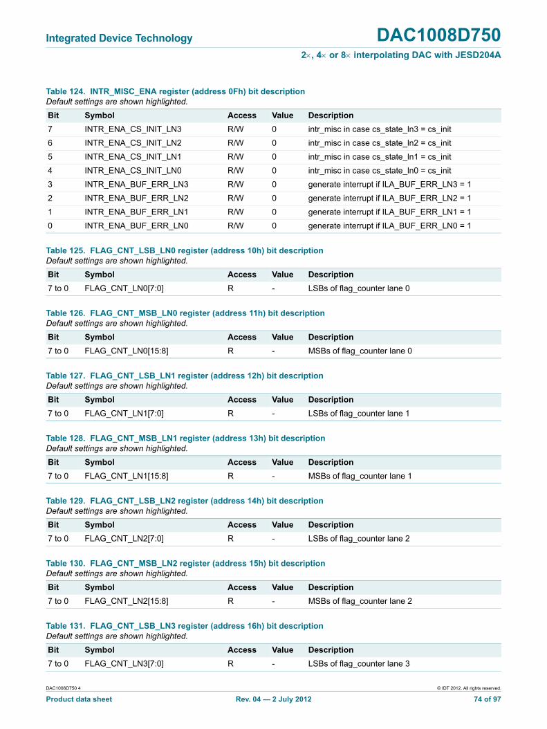
Integrated Device Technology DAC1008D7502, 4 or 8 interpolating DAC with JESD204A
Table 124. INTR_MISC_ENA register (address 0Fh) bit descriptionDefault settings are shown highlighted.
Bit Symbol Access Value Description
7 INTR_ENA_CS_INIT_LN3 R/W 0 intr_misc in case cs_state_ln3 = cs_init
6 INTR_ENA_CS_INIT_LN2 R/W 0 intr_misc in case cs_state_ln2 = cs_init
5 INTR_ENA_CS_INIT_LN1 R/W 0 intr_misc in case cs_state_ln1 = cs_init
4 INTR_ENA_CS_INIT_LN0 R/W 0 intr_misc in case cs_state_ln0 = cs_init
3 INTR_ENA_BUF_ERR_LN3 R/W 0 generate interrupt if ILA_BUF_ERR_LN3 = 1
2 INTR_ENA_BUF_ERR_LN2 R/W 0 generate interrupt if ILA_BUF_ERR_LN2 = 1
1 INTR_ENA_BUF_ERR_LN1 R/W 0 generate interrupt if ILA_BUF_ERR_LN1 = 1
0 INTR_ENA_BUF_ERR_LN0 R/W 0 generate interrupt if ILA_BUF_ERR_LN0 = 1
Table 125. FLAG_CNT_LSB_LN0 register (address 10h) bit descriptionDefault settings are shown highlighted.
Bit Symbol Access Value Description
7 to 0 FLAG_CNT_LN0[7:0] R - LSBs of flag_counter lane 0
Table 126. FLAG_CNT_MSB_LN0 register (address 11h) bit descriptionDefault settings are shown highlighted.
Bit Symbol Access Value Description
7 to 0 FLAG_CNT_LN0[15:8] R - MSBs of flag_counter lane 0
Table 127. FLAG_CNT_LSB_LN1 register (address 12h) bit descriptionDefault settings are shown highlighted.
Bit Symbol Access Value Description
7 to 0 FLAG_CNT_LN1[7:0] R - LSBs of flag_counter lane 1
Table 128. FLAG_CNT_MSB_LN1 register (address 13h) bit descriptionDefault settings are shown highlighted.
Bit Symbol Access Value Description
7 to 0 FLAG_CNT_LN1[15:8] R - MSBs of flag_counter lane 1
Table 129. FLAG_CNT_LSB_LN2 register (address 14h) bit descriptionDefault settings are shown highlighted.
Bit Symbol Access Value Description
7 to 0 FLAG_CNT_LN2[7:0] R - LSBs of flag_counter lane 2
Table 130. FLAG_CNT_MSB_LN2 register (address 15h) bit descriptionDefault settings are shown highlighted.
Bit Symbol Access Value Description
7 to 0 FLAG_CNT_LN2[15:8] R - MSBs of flag_counter lane 2
Table 131. FLAG_CNT_LSB_LN3 register (address 16h) bit descriptionDefault settings are shown highlighted.
Bit Symbol Access Value Description
7 to 0 FLAG_CNT_LN3[7:0] R - LSBs of flag_counter lane 3
DAC1008D750 4 © IDT 2012. All rights reserved.
Product data sheet Rev. 04 — 2 July 2012 74 of 97

Integrated Device Technology DAC1008D7502, 4 or 8 interpolating DAC with JESD204A
Table 132. FLAG_CNT_MSB_LN3 register (address 17h) bit descriptionDefault settings are shown highlighted.
Bit Symbol Access Value Description
7 to 0 FLAG_CNT_LN3[15:8] R - MSBs of flag_counter lane 3
Table 133. BER_LEVEL_LSB register (address 18h) bit descriptionDefault settings are shown highlighted.
Bit Symbol Access Value Description
7 to 0 BER_LEVEL[7:0] R/W 00h LSBs level used for simple (DC) BER-measurement
Table 134. BER_LEVEL_MSB register (address 19h) bit descriptionDefault settings are shown highlighted.
Bit Symbol Access Value Description
7 to 0 BER_LEVEL[15:8] R/W 00h MSBs level used for simple (DC) BER-measurement
Table 135. INTR_ENA register (address 1Ah) bit description
Bit Symbol Access Value Description
7 INTR_ENA_NIT R/W not-in-table interrupt
0 no action
1 nit-error in ln<x> affects i_ln<x>
6 INTR_ENA_DISP R/W disparity-error interrupt
0 no action
1 disparity-error in ln<x> affects i_ln<x>
5 INTR_ENA_KOUT R/W K-character interrupt
0 no action
1 detection K-control character in ln<x> affects i_ln<x>
4 INTR_ENA_KOUT_UNEXP R/W unexpected K-character interrupt
0 no action
1 detection unexpected K-character in ln<x> affects i_ln<x>
3 INTR_ENA_K28_7 R/W K28_7 interrupt
0 no action
1 detection K28_7 in ln<x> affects i_ln<x>
2 INTR_ENA_K28_5 R/W K28_5 interrupt
0 no action
1 detection K28_5 in ln<x> affects i_ln<x>
1 INTR_ENA_K28_3 R/W K28_3 interrupt
0 no action
1 detection K28_3 in ln<x> affects i_ln<x>
0 INTR_ENA_MISC R/W miscellaneous interrupt
0 no action
1 detection depends on intr_misc_ena (see Table 124)
DAC1008D750 4 © IDT 2012. All rights reserved.
Product data sheet Rev. 04 — 2 July 2012 75 of 97
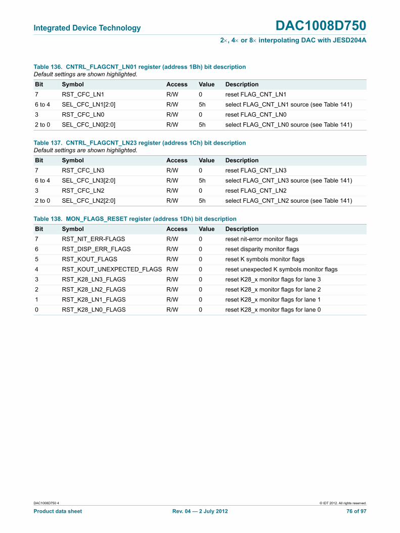
Integrated Device Technology DAC1008D7502, 4 or 8 interpolating DAC with JESD204A
Table 136. CNTRL_FLAGCNT_LN01 register (address 1Bh) bit descriptionDefault settings are shown highlighted.
Bit Symbol Access Value Description
7 RST_CFC_LN1 R/W 0 reset FLAG_CNT_LN1
6 to 4 SEL_CFC_LN1[2:0] R/W 5h select FLAG_CNT_LN1 source (see Table 141)
3 RST_CFC_LN0 R/W 0 reset FLAG_CNT_LN0
2 to 0 SEL_CFC_LN0[2:0] R/W 5h select FLAG_CNT_LN0 source (see Table 141)
Table 137. CNTRL_FLAGCNT_LN23 register (address 1Ch) bit descriptionDefault settings are shown highlighted.
Bit Symbol Access Value Description
7 RST_CFC_LN3 R/W 0 reset FLAG_CNT_LN3
6 to 4 SEL_CFC_LN3[2:0] R/W 5h select FLAG_CNT_LN3 source (see Table 141)
3 RST_CFC_LN2 R/W 0 reset FLAG_CNT_LN2
2 to 0 SEL_CFC_LN2[2:0] R/W 5h select FLAG_CNT_LN2 source (see Table 141)
Table 138. MON_FLAGS_RESET register (address 1Dh) bit description
Bit Symbol Access Value Description
7 RST_NIT_ERR-FLAGS R/W 0 reset nit-error monitor flags
6 RST_DISP_ERR_FLAGS R/W 0 reset disparity monitor flags
5 RST_KOUT_FLAGS R/W 0 reset K symbols monitor flags
4 RST_KOUT_UNEXPECTED_FLAGS R/W 0 reset unexpected K symbols monitor flags
3 RST_K28_LN3_FLAGS R/W 0 reset K28_x monitor flags for lane 3
2 RST_K28_LN2_FLAGS R/W 0 reset K28_x monitor flags for lane 2
1 RST_K28_LN1_FLAGS R/W 0 reset K28_x monitor flags for lane 1
0 RST_K28_LN0_FLAGS R/W 0 reset K28_x monitor flags for lane 0
DAC1008D750 4 © IDT 2012. All rights reserved.
Product data sheet Rev. 04 — 2 July 2012 76 of 97

Integrated Device Technology DAC1008D7502, 4 or 8 interpolating DAC with JESD204A
Table 139. DBG_CNTRL register (address 1Eh) bit description
Bit Symbol Access Value Description
7 BER_MODE R/W simple BER-measurement
0 no action
1 simple BER-measurement enabled
6 INTR_CLEAR R/W interrupts clear
0 no action
1 clear interrupts (to '1')
5 to 3 INTR_MODE[2:0] R/W interrupt settings
000 global interrupt depends on lane 0
001 global interrupt depends on lane 1
010 global interrupt depends on lane 2
011 global interrupt depends on lane 3
100 global interrupt depends on lane 0 or lane 1
101 global interrupt depends on lane 2 or lane 3
110 global interrupt depends on lane 0 or lane 1 or lane 2 or lane 3
111 no interrupt
Table 140. PAGE_ADDRESS register (address 1Fh) bit description
Bit Symbol Access Value Description
2 to 0 PAGE[2:0] R/W 0h page_address
Table 141. Counter sourceDefault settings are shown highlighted.
SEL_CFC_LNn[2:0] Source
000 not-in-table error
001 disparity error
010 K symbol found
011 unexpected K symbol found
100 K28_7 (/F/) symbol found
101 K28_5 (/K/) symbol found
110 K28_3 (/A/) symbol found
111 K28_0 (/R/) symbol found
Table 142. Code group synchronization state machine
CS_STATE_LNn[1:0] Definition
00 looking for K28_5 (/K/) symbol
01 four consecutive K28_5 (/K/) symbols have been received
10 code group synchronization achieved
11 not applicable
DAC1008D750 4 © IDT 2012. All rights reserved.
Product data sheet Rev. 04 — 2 July 2012 77 of 97

xxxxxxxxxxxxxxxxxxxxx xxxxxxxxxxxxxxxxxxxxxxxxxx xxxxxxx x x x xxxxxxxxxxxxxxxxxxxxxxxxxxxxxx xxxxxxxxxxxxxxxxxxx xx xx xxxxx xxxxxxxxxxxxxxxxxxxxxxxxxxx xxxxxxxxxxxxxxxxxxx xxxxxx xxxxxxxxxxxxxxxxxxxxxxxxxxxxxxxxxxx xxxxxxxxxxxx x x xxxxxxxxxxxxxxxxxxxxx xxxxxxxxxxxxxxxxxxxxxxxxxxxxxx xxxxx xxxxxxxxxxxxxxxxxxxxxxxxxxxxxxxxxxxxxxxxxxxxxxxxxx xxxxxxxx xxxxxxxxxxxxxxxxxxxxxxxxx xxxxxxxxxxxxxxxxxxxx xxx
DA
C100
8D750
4
Pro
du
ct data sh
eetR
ev. 04 —
2 July 2012
78 o
f 97
Integ
rated D
evice Techn
olo
gy
DA
C1008D
7502, 4 o
r 8 inte
rpo
lating
DA
C w
ith J
ES
D20
4A10.15.2.11 Page 6 allocation map description
Table 143. Page 6 register allocation map
Default[1]
b0 Bin Hex
uuuuuuuu 0xuu
uuuuuuuu 0xuu
uuuuuuuu 0xuu
uuuuuuuu 0xuu
uuuuuuuu 0xuu
uuuuuuuu 0xuu
uuuuuuuu 0xuu
uuuuuuuu 0xuu
uuuuuuuu 0xuu
uuuuuuuu 0xuu
uuuuuuuu 0xuu
uuuuuuuu 0xuu
uuuuuuuu 0xuu
uuuuuuuu 0xuu
uuuuuuuu 0xuu
uuuuuuuu 0xuu
uuuuuuuu 0xuu
uuuuuuuu 0xuu
uuuuuuuu 0xuu
uuuuuuuu 0xuu
uuuuuuuu 0xuu
uuuuuuuu 0xuu
uuuuuuuu 0xuu
uuuuuuuu 0xuu
uuuuuuuu 0xuu
uuuuuuuu 0xuu
© ID
T 20
12. All rights reserved
.
Address Register name R/W Bit definition
b7 b6 b5 b4 b3 b2 b1
0 00h LN0_CFG_0 R LN0_DID[7:0]
1 01h LN0_CFG_1 R - - - - LN0_BID[3:0]
2 02h LN0_CFG_2 R - - - LN0_LID[4:0]
3 03h LN0_CFG_3 R LN0_SCR - - LN0_L[4:0]
4 04h LN0_CFG_4 R LN0_F[7:0]
5 05h LN0_CFG_5 R - - - LN0_K[4:0]
6 06h LN0_CFG_6 R LN0_M[7:0]
7 07h LN0_CFG_7 R LN0_CS[1:0] - LN0_N[4:0]
8 08h LN0_CFG_8 R - - - LN0_N’[4:0]
9 09h LN0_CFG_9 R - - - LN0_S[4:0]
10 0Ah LN0_CFG_10 R LN0_HD - - LN0_CF[4:0]
11 0Bh LN0_CFG_11 R LN0_RES1[7:0]
12 0Ch LN0_CFG_12 R LN0_RES2[7:0]
13 0Dh LN0_CFG_13 R LN0_FCHK[7:0]
16 10h LN1_CFG_0 R LN1_DID[7:0]
17 11h LN1_CFG_1 R - - - - LN1_BID[3:0]
18 12h LN1_CFG_2 R - - - LN1_LID[4:0]
19 13h LN1_CFG_3 R LN1_SCR - - LN1_L[4:0]
20 14h LN1_CFG_4 R LN1_F[7:0]
21 15h LN1_CFG_5 R - - - LN1_K[4:0]
22 16h LN1_CFG_6 R LN1_M[7:0]
23 17h LN1_CFG_7 R LN1_CS[1:0] - LN1_N[4:0]
24 18h LN1_CFG_8 R - - - LN1_N’[4:0]
25 19h LN1_CFG_9 R - - - LN1_S[4:0]
26 1Ah LN1_CFG_10 R LN1_HD - - LN1_CF[4:0]
27 1Bh LN1_CFG_11 R LN1_RES1[7:0]

xxxxxxxxxxxxxxxxxxxxx xxxxxxxxxxxxxxxxxxxxxxxxxx xxxxxxx x x x xxxxxxxxxxxxxxxxxxxxxxxxxxxxxx xxxxxxxxxxxxxxxxxxx xx xx xxxxx xxxxxxxxxxxxxxxxxxxxxxxxxxx xxxxxxxxxxxxxxxxxxx xxxxxx xxxxxxxxxxxxxxxxxxxxxxxxxxxxxxxxxxx xxxxxxxxxxxx x x xxxxxxxxxxxxxxxxxxxxx xxxxxxxxxxxxxxxxxxxxxxxxxxxxxx xxxxx xxxxxxxxxxxxxxxxxxxxxxxxxxxxxxxxxxxxxxxxxxxxxxxxxx xxxxxxxx xxxxxxxxxxxxxxxxxxxxxxxxx xxxxxxxxxxxxxxxxxxxx xxx
DA
C100
8D750
4
Pro
du
ct data sh
eetR
ev. 04 —
2 July 2012
79 o
f 97
Integ
rated D
evice Techn
olo
gy
DA
C1008D
7502, 4 o
r 8 inte
rpo
lating
DA
C w
ith J
ES
D20
4A
uuuuuuuu 0xuu
uuuuuuuu 0xuu
0] 00000000 00h
Table 143. Page 6 register allocation map …continued
Address Register name R/W Bit definition Default[1]
b7 b6 b5 b4 b3 b2 b1 b0 Bin Hex
© ID
T 20
12. All rights reserved
.
[1] u = undefined at power-up or after reset.
28 1Ch LN1_CFG_12 R LN1_RES2[7:0]
29 1Dh LN1_CFG_13 R LN1_FCHK[7:0]
31 1Fh PAGE_ADDRESS R/W - - - - - PAGE[2:
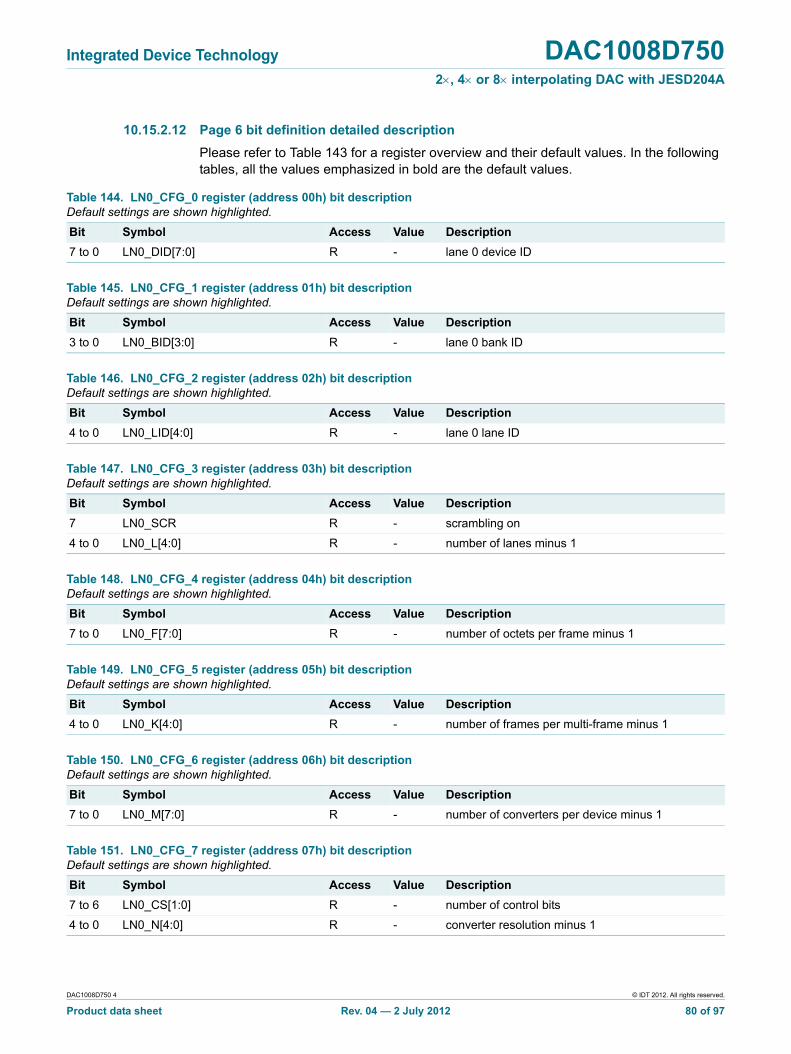
Integrated Device Technology DAC1008D7502, 4 or 8 interpolating DAC with JESD204A
10.15.2.12 Page 6 bit definition detailed description
Please refer to Table 143 for a register overview and their default values. In the following tables, all the values emphasized in bold are the default values.
Table 144. LN0_CFG_0 register (address 00h) bit descriptionDefault settings are shown highlighted.
Bit Symbol Access Value Description
7 to 0 LN0_DID[7:0] R - lane 0 device ID
Table 145. LN0_CFG_1 register (address 01h) bit descriptionDefault settings are shown highlighted.
Bit Symbol Access Value Description
3 to 0 LN0_BID[3:0] R - lane 0 bank ID
Table 146. LN0_CFG_2 register (address 02h) bit descriptionDefault settings are shown highlighted.
Bit Symbol Access Value Description
4 to 0 LN0_LID[4:0] R - lane 0 lane ID
Table 147. LN0_CFG_3 register (address 03h) bit descriptionDefault settings are shown highlighted.
Bit Symbol Access Value Description
7 LN0_SCR R - scrambling on
4 to 0 LN0_L[4:0] R - number of lanes minus 1
Table 148. LN0_CFG_4 register (address 04h) bit descriptionDefault settings are shown highlighted.
Bit Symbol Access Value Description
7 to 0 LN0_F[7:0] R - number of octets per frame minus 1
Table 149. LN0_CFG_5 register (address 05h) bit descriptionDefault settings are shown highlighted.
Bit Symbol Access Value Description
4 to 0 LN0_K[4:0] R - number of frames per multi-frame minus 1
Table 150. LN0_CFG_6 register (address 06h) bit descriptionDefault settings are shown highlighted.
Bit Symbol Access Value Description
7 to 0 LN0_M[7:0] R - number of converters per device minus 1
Table 151. LN0_CFG_7 register (address 07h) bit descriptionDefault settings are shown highlighted.
Bit Symbol Access Value Description
7 to 6 LN0_CS[1:0] R - number of control bits
4 to 0 LN0_N[4:0] R - converter resolution minus 1
DAC1008D750 4 © IDT 2012. All rights reserved.
Product data sheet Rev. 04 — 2 July 2012 80 of 97

Integrated Device Technology DAC1008D7502, 4 or 8 interpolating DAC with JESD204A
Table 152. LN0_CFG_8 register (address 08h) bit descriptionDefault settings are shown highlighted.
Bit Symbol Access Value Description
4 to 0 LN0_N’[4:0] R - number of bits per sample minus 1
Table 153. LN0_CFG_9 register (address 09h) bit descriptionDefault settings are shown highlighted.
Bit Symbol Access Value Description
4 to 0 LN0_S[4:0] R - number of samples per converter per frame cycle minus 1
Table 154. LN0_CFG_10 register (address 0Ah) bit descriptionDefault settings are shown highlighted.
Bit Symbol Access Value Description
7 LN0_HD R - high density
4 to 0 LN0_CF[4:0] R - number of control words per frame cycle
Table 155. LN0_CFG_11 register (address 0Bh) bit descriptionDefault settings are shown highlighted.
Bit Symbol Access Value Description
7 to 0 LN0_RES1[7:0] R - lane 0 reserved field
Table 156. LN0_CFG_12 register (address 0Ch) bit descriptionDefault settings are shown highlighted.
Bit Symbol Access Value Description
7 to 0 LN0_RES2[7:0] R - lane 0 reserved field
Table 157. LN0_CFG_13 register (address 0Dh) bit descriptionDefault settings are shown highlighted.
Bit Symbol Access Value Description
7 to 0 LN0_FCHK[7:0] R - lane 0 checksum
Table 158. LN1_CFG_0 register (address 10h) bit descriptionDefault settings are shown highlighted.
Bit Symbol Access Value Description
7 to 0 LN1_DID[7:0] R - lane 1 device ID
Table 159. LN1_CFG_1 register (address 11h) bit descriptionDefault settings are shown highlighted.
Bit Symbol Access Value Description
3 to 0 LN1_BID[3:0] R - lane 1 bank ID
Table 160. LN1_CFG_2 register (address 12h) bit descriptionDefault settings are shown highlighted.
Bit Symbol Access Value Description
4 to 0 LN1_LID[4:0] R - lane 1 lane ID
DAC1008D750 4 © IDT 2012. All rights reserved.
Product data sheet Rev. 04 — 2 July 2012 81 of 97

Integrated Device Technology DAC1008D7502, 4 or 8 interpolating DAC with JESD204A
Table 161. LN1_CFG_3 register (address 13h) bit descriptionDefault settings are shown highlighted.
Bit Symbol Access Value Description
7 LN1_SCR R - scrambling on
4 to 0 LN1_L[4:0] R - number of lanes minus 1
Table 162. LN1_CFG_4 register (address 14h) bit descriptionDefault settings are shown highlighted.
Bit Symbol Access Value Description
7 to 0 LN1_F[7:0] R - number of octets per frame minus 1
Table 163. LN1_CFG_5 register (address 15h) bit descriptionDefault settings are shown highlighted.
Bit Symbol Access Value Description
4 to 0 LN1_K[4:0] R - number of frames per multiframe minus 1
Table 164. LN1_CFG_6 register (address 16h) bit descriptionDefault settings are shown highlighted.
Bit Symbol Access Value Description
7 to 0 LN1_M[7:0] R - number of converters per device minus 1
Table 165. LN1_CFG_7 register (address 17h) bit descriptionDefault settings are shown highlighted.
Bit Symbol Access Value Description
7 to 6 LN1_CS[1:0] R - number of control bits
4 to 0 LN1_N[4:0] R - converter resolution minus 1
Table 166. LN1_CFG_8 register (address 18h) bit descriptionDefault settings are shown highlighted.
Bit Symbol Access Value Description
4 to 0 LN1_N’[4:0] R - number of bits per sample minus 1
Table 167. LN1_CFG_9 register (address 19h) bit descriptionDefault settings are shown highlighted.
Bit Symbol Access Value Description
4 to 0 LN1_S[4:0] R - number of samples per converter per frame cycle minus 1
Table 168. LN1_CFG_10 register (address 1Ah) bit descriptionDefault settings are shown highlighted.
Bit Symbol Access Value Description
7 to 6 LN1_HD R - high density
4 to 0 LN1_CF[4:0] R - number of control words per frame cycle
DAC1008D750 4 © IDT 2012. All rights reserved.
Product data sheet Rev. 04 — 2 July 2012 82 of 97
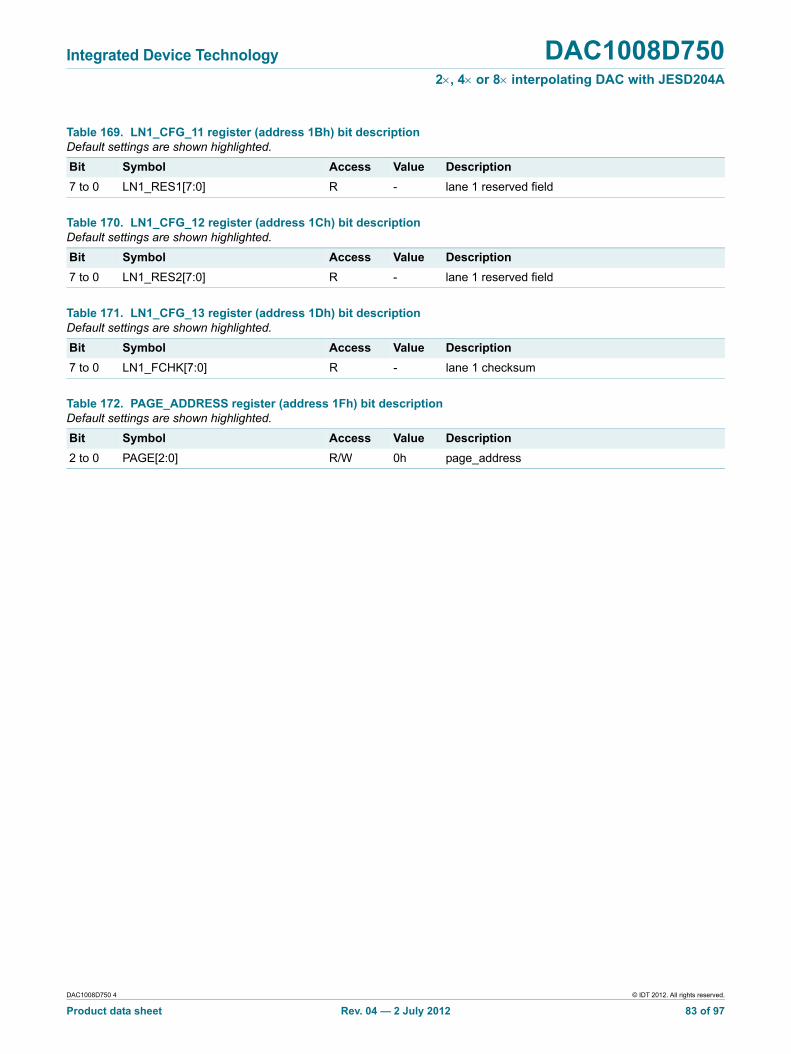
Integrated Device Technology DAC1008D7502, 4 or 8 interpolating DAC with JESD204A
Table 169. LN1_CFG_11 register (address 1Bh) bit descriptionDefault settings are shown highlighted.
Bit Symbol Access Value Description
7 to 0 LN1_RES1[7:0] R - lane 1 reserved field
Table 170. LN1_CFG_12 register (address 1Ch) bit descriptionDefault settings are shown highlighted.
Bit Symbol Access Value Description
7 to 0 LN1_RES2[7:0] R - lane 1 reserved field
Table 171. LN1_CFG_13 register (address 1Dh) bit descriptionDefault settings are shown highlighted.
Bit Symbol Access Value Description
7 to 0 LN1_FCHK[7:0] R - lane 1 checksum
Table 172. PAGE_ADDRESS register (address 1Fh) bit descriptionDefault settings are shown highlighted.
Bit Symbol Access Value Description
2 to 0 PAGE[2:0] R/W 0h page_address
DAC1008D750 4 © IDT 2012. All rights reserved.
Product data sheet Rev. 04 — 2 July 2012 83 of 97

xxxxxxxxxxxxxxxxxxxxx xxxxxxxxxxxxxxxxxxxxxxxxxx xxxxxxx x x x xxxxxxxxxxxxxxxxxxxxxxxxxxxxxx xxxxxxxxxxxxxxxxxxx xx xx xxxxx xxxxxxxxxxxxxxxxxxxxxxxxxxx xxxxxxxxxxxxxxxxxxx xxxxxx xxxxxxxxxxxxxxxxxxxxxxxxxxxxxxxxxxx xxxxxxxxxxxx x x xxxxxxxxxxxxxxxxxxxxx xxxxxxxxxxxxxxxxxxxxxxxxxxxxxx xxxxx xxxxxxxxxxxxxxxxxxxxxxxxxxxxxxxxxxxxxxxxxxxxxxxxxx xxxxxxxx xxxxxxxxxxxxxxxxxxxxxxxxx xxxxxxxxxxxxxxxxxxxx xxx
DA
C100
8D750
4
Pro
du
ct data sh
eetR
ev. 04 —
2 July 2012
84 o
f 97
Integ
rated D
evice Techn
olo
gy
DA
C1008D
7502, 4 o
r 8 inte
rpo
lating
DA
C w
ith J
ES
D20
4A10.15.2.13 Page 7 allocation map description
Table 173. Page 7 register allocation map
Default[1]
b0 Bin Hex
uuuuuuuu 0xuu
uuuuuuuu 0xuu
uuuuuuuu 0xuu
uuuuuuuu 0xuu
uuuuuuuu 0xuu
uuuuuuuu 0xuu
uuuuuuuu 0xuu
uuuuuuuu 0xuu
uuuuuuuu 0xuu
uuuuuuuu 0xuu
uuuuuuuu 0xuu
uuuuuuuu 0xuu
uuuuuuuu 0xuu
uuuuuuuu 0xuu
uuuuuuuu 0xuu
uuuuuuuu 0xuu
uuuuuuuu 0xuu
uuuuuuuu 0xuu
uuuuuuuu 0xuu
uuuuuuuu 0xuu
uuuuuuuu 0xuu
uuuuuuuu 0xuu
uuuuuuuu 0xuu
uuuuuuuu 0xuu
uuuuuuuu 0xuu
uuuuuuuu 0xuu
© ID
T 20
12. All rights reserved
.
Address Register name R/W Bit definition
b7 b6 b5 b4 b3 b2 b1
0 00h LN2_CFG_0 R LN2_DID[7:0]
1 01h LN2_CFG_1 R - - - - LN2_BID[3:0]
2 02h LN2_CFG_2 R - - - LN2_LID[4:0]
3 03h LN2_CFG_3 R LN2_SCR - - LN2_L[4:0]
4 04h LN2_CFG_4 R LN2_F[7:0]
5 05h LN2_CFG_5 R - - - LN2_K[4:0]
6 06h LN2_CFG_6 R LN2_M[7:0]
7 07h LN2_CFG_7 R LN2_CS[1:0] - LN2_N[4:0]
8 08h LN2_CFG_8 R - - - LN2_N’[4:0]
9 09h LN2_CFG_9 R - - - LN2_S[4:0]
10 0Ah LN2_CFG_10 R LN2_HD - - LN2_CF[4:0]
11 0Bh LN2_CFG_11 R LN2_RES1[7:0]
12 0Ch LN2_CFG_12 R LN2_RES2[7:0]
13 0Dh LN2_CFG_13 R LN2_FCHK[7:0]
16 10h LN3_CFG_0 R LN3_DID[7:0]
17 11h LN3_CFG_1 R - - - - LN3_BID[3:0]
18 12h LN3_CFG_2 R - - - LN3_LID[4:0]
19 13h LN3_CFG_3 R LN3_SCR - - LN3_L[4:0]
20 14h LN3_CFG_4 R LN3_F[7:0]
21 15h LN3_CFG_5 R - - - LN3_K[4:0]
22 16h LN3_CFG_6 R LN3_M[7:0]
23 17h LN3_CFG_7 R LN3_CS[1:0] - LN3_N[4:0]
24 18h LN3_CFG_8 R - - - LN3_N’[4:0]
25 19h LN3_CFG_9 R - - - LN3_S[4:0]
26 1Ah LN3_CFG_10 R LN3_HD - - LN3_CF[4:0]
27 1Bh LN3_CFG_11 R LN3_RES1[7:0]
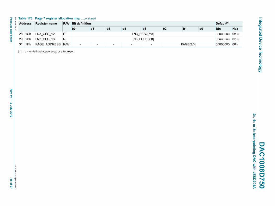
xxxxxxxxxxxxxxxxxxxxx xxxxxxxxxxxxxxxxxxxxxxxxxx xxxxxxx x x x xxxxxxxxxxxxxxxxxxxxxxxxxxxxxx xxxxxxxxxxxxxxxxxxx xx xx xxxxx xxxxxxxxxxxxxxxxxxxxxxxxxxx xxxxxxxxxxxxxxxxxxx xxxxxx xxxxxxxxxxxxxxxxxxxxxxxxxxxxxxxxxxx xxxxxxxxxxxx x x xxxxxxxxxxxxxxxxxxxxx xxxxxxxxxxxxxxxxxxxxxxxxxxxxxx xxxxx xxxxxxxxxxxxxxxxxxxxxxxxxxxxxxxxxxxxxxxxxxxxxxxxxx xxxxxxxx xxxxxxxxxxxxxxxxxxxxxxxxx xxxxxxxxxxxxxxxxxxxx xxx
DA
C100
8D750
4
Pro
du
ct data sh
eetR
ev. 04 —
2 July 2012
85 o
f 97
Integ
rated D
evice Techn
olo
gy
DA
C1008D
7502, 4 o
r 8 inte
rpo
lating
DA
C w
ith J
ES
D20
4A
uuuuuuuu 0xuu
uuuuuuuu 0xuu
0] 00000000 00h
Table 173. Page 7 register allocation map …continued
Address Register name R/W Bit definition Default[1]
b7 b6 b5 b4 b3 b2 b1 b0 Bin Hex
© ID
T 20
12. All rights reserved
.
[1] u = undefined at power-up or after reset.
28 1Ch LN3_CFG_12 R LN3_RES2[7:0]
29 1Dh LN3_CFG_13 R LN3_FCHK[7:0]
31 1Fh PAGE_ADDRESS R/W - - - - - PAGE[2:

Integrated Device Technology DAC1008D7502, 4 or 8 interpolating DAC with JESD204A
10.15.2.14 Page 7 bit definition detailed description
Please refer to Table 173 for a register overview and their default values. In the following tables, all the values emphasized in bold are the default values.
Table 174. LN2_CFG_0 register (address 00h) bit descriptionDefault settings are shown highlighted.
Bit Symbol Access Value Description
7 to 0 LN2_DID[7:0] R - lane 2 device ID
Table 175. LN2_CFG_1 register (address 01h) bit descriptionDefault settings are shown highlighted.
Bit Symbol Access Value Description
3 to 0 LN2_BID[3:0] R - lane 2 bank ID
Table 176. LN2_CFG_2 register (address 02h) bit descriptionDefault settings are shown highlighted.
Bit Symbol Access Value Description
4 to 0 LN2_LID[4:0] R - lane 2 lane ID
Table 177. LN2_CFG_3 register (address 03h) bit descriptionDefault settings are shown highlighted.
Bit Symbol Access Value Description
7 LN2_SCR R - scrambling on
4 to 0 LN2_L[4:0] R - number of lanes minus 1
Table 178. LN2_CFG_4 register (address 04h) bit descriptionDefault settings are shown highlighted.
Bit Symbol Access Value Description
7 to 0 LN2_F[7:0] R - number of octets per frame minus 1
Table 179. LN2_CFG_5 register (address 05h) bit descriptionDefault settings are shown highlighted.
Bit Symbol Access Value Description
4 to 0 LN2_K[4:0] R - number of frames per multiframe minus 1
Table 180. LN2_CFG_6 register (address 06h) bit descriptionDefault settings are shown highlighted.
Bit Symbol Access Value Description
7 to 0 LN2_M[7:0] R - number of converters per device minus 1
Table 181. LN2_CFG_7 register (address 07h) bit descriptionDefault settings are shown highlighted.
Bit Symbol Access Value Description
7 to 6 LN2_CS[1:0] R - number of control bits
4 to 0 LN2_N[4:0] R - converter resolution minus 1
DAC1008D750 4 © IDT 2012. All rights reserved.
Product data sheet Rev. 04 — 2 July 2012 86 of 97
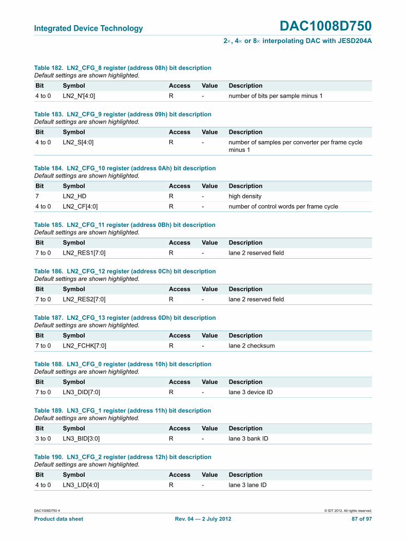
Integrated Device Technology DAC1008D7502, 4 or 8 interpolating DAC with JESD204A
Table 182. LN2_CFG_8 register (address 08h) bit descriptionDefault settings are shown highlighted.
Bit Symbol Access Value Description
4 to 0 LN2_N'[4:0] R - number of bits per sample minus 1
Table 183. LN2_CFG_9 register (address 09h) bit descriptionDefault settings are shown highlighted.
Bit Symbol Access Value Description
4 to 0 LN2_S[4:0] R - number of samples per converter per frame cycle minus 1
Table 184. LN2_CFG_10 register (address 0Ah) bit descriptionDefault settings are shown highlighted.
Bit Symbol Access Value Description
7 LN2_HD R - high density
4 to 0 LN2_CF[4:0] R - number of control words per frame cycle
Table 185. LN2_CFG_11 register (address 0Bh) bit descriptionDefault settings are shown highlighted.
Bit Symbol Access Value Description
7 to 0 LN2_RES1[7:0] R - lane 2 reserved field
Table 186. LN2_CFG_12 register (address 0Ch) bit descriptionDefault settings are shown highlighted.
Bit Symbol Access Value Description
7 to 0 LN2_RES2[7:0] R - lane 2 reserved field
Table 187. LN2_CFG_13 register (address 0Dh) bit descriptionDefault settings are shown highlighted.
Bit Symbol Access Value Description
7 to 0 LN2_FCHK[7:0] R - lane 2 checksum
Table 188. LN3_CFG_0 register (address 10h) bit descriptionDefault settings are shown highlighted.
Bit Symbol Access Value Description
7 to 0 LN3_DID[7:0] R - lane 3 device ID
Table 189. LN3_CFG_1 register (address 11h) bit descriptionDefault settings are shown highlighted.
Bit Symbol Access Value Description
3 to 0 LN3_BID[3:0] R - lane 3 bank ID
Table 190. LN3_CFG_2 register (address 12h) bit descriptionDefault settings are shown highlighted.
Bit Symbol Access Value Description
4 to 0 LN3_LID[4:0] R - lane 3 lane ID
DAC1008D750 4 © IDT 2012. All rights reserved.
Product data sheet Rev. 04 — 2 July 2012 87 of 97

Integrated Device Technology DAC1008D7502, 4 or 8 interpolating DAC with JESD204A
Table 191. LN3_CFG_3 register (address 13h) bit descriptionDefault settings are shown highlighted.
Bit Symbol Access Value Description
7 LN3_SCR R - scrambling on
4 to 0 LN3_L[4:0] R - number of lanes minus 1
Table 192. LN3_CFG_4 register (address 14h) bit descriptionDefault settings are shown highlighted.
Bit Symbol Access Value Description
7 to 0 LN3_F[7:0] R - number of octets per frame minus 1
Table 193. LN3_CFG_5 register (address 15h) bit descriptionDefault settings are shown highlighted.
Bit Symbol Access Value Description
4 to 0 LN3_K[4:0] R - number of frames per multiframe minus 1
Table 194. LN3_CFG_6 register (address 16h) bit descriptionDefault settings are shown highlighted.
Bit Symbol Access Value Description
7 to 0 LN3_M[7:0] R - number of converters per device minus 1
Table 195. LN3_CFG_7 register (address 17h) bit descriptionDefault settings are shown highlighted.
Bit Symbol Access Value Description
7 to 6 LN3_CS[1:0] R - number of control bits
4 to 0 LN3_N[4:0] R - converter resolution minus 1
Table 196. LN3_CFG_8 register (address 18h) bit descriptionDefault settings are shown highlighted.
Bit Symbol Access Value Description
4 to 0 LN3_N'[4:0] R - number of bits per sample minus 1
Table 197. LN3_CFG_9 register (address 19h) bit descriptionDefault settings are shown highlighted.
Bit Symbol Access Value Description
4 to 0 LN3_S[4:0] R - number of samples per converter per frame cycle minus 1
Table 198. LN3_CFG_10 register (address 1Ah) bit descriptionDefault settings are shown highlighted.
Bit Symbol Access Value Description
7 LN3_HD R - high density
4 to 0 LN3_CF[4:0] R - number of control words per frame cycle
DAC1008D750 4 © IDT 2012. All rights reserved.
Product data sheet Rev. 04 — 2 July 2012 88 of 97

Integrated Device Technology DAC1008D7502, 4 or 8 interpolating DAC with JESD204A
Table 199. LN3_CFG_11 register (address 1Bh) bit descriptionDefault settings are shown highlighted.
Bit Symbol Access Value Description
7 to 0 LN3_RES1[7:0] R - lane 3 reserved field
Table 200. LN3_CFG_12 register (address 1Ch) bit descriptionDefault settings are shown highlighted.
Bit Symbol Access Value Description
7 to 0 LN3_RES2[7:0] R - lane 3 reserved field
Table 201. LN3_CFG_13 register (address 1Dh) bit descriptionDefault settings are shown highlighted.
Bit Symbol Access Value Description
7 to 0 LN3_FCHK[7:0] R - lane 3 checksum
Table 202. PAGE_ADDRESS register (address 1Fh) bit descriptionDefault settings are shown highlighted.
Bit Symbol Access Value Description
2 to 0 PAGE[2:0] R/W 0h page_address
DAC1008D750 4 © IDT 2012. All rights reserved.
Product data sheet Rev. 04 — 2 July 2012 89 of 97
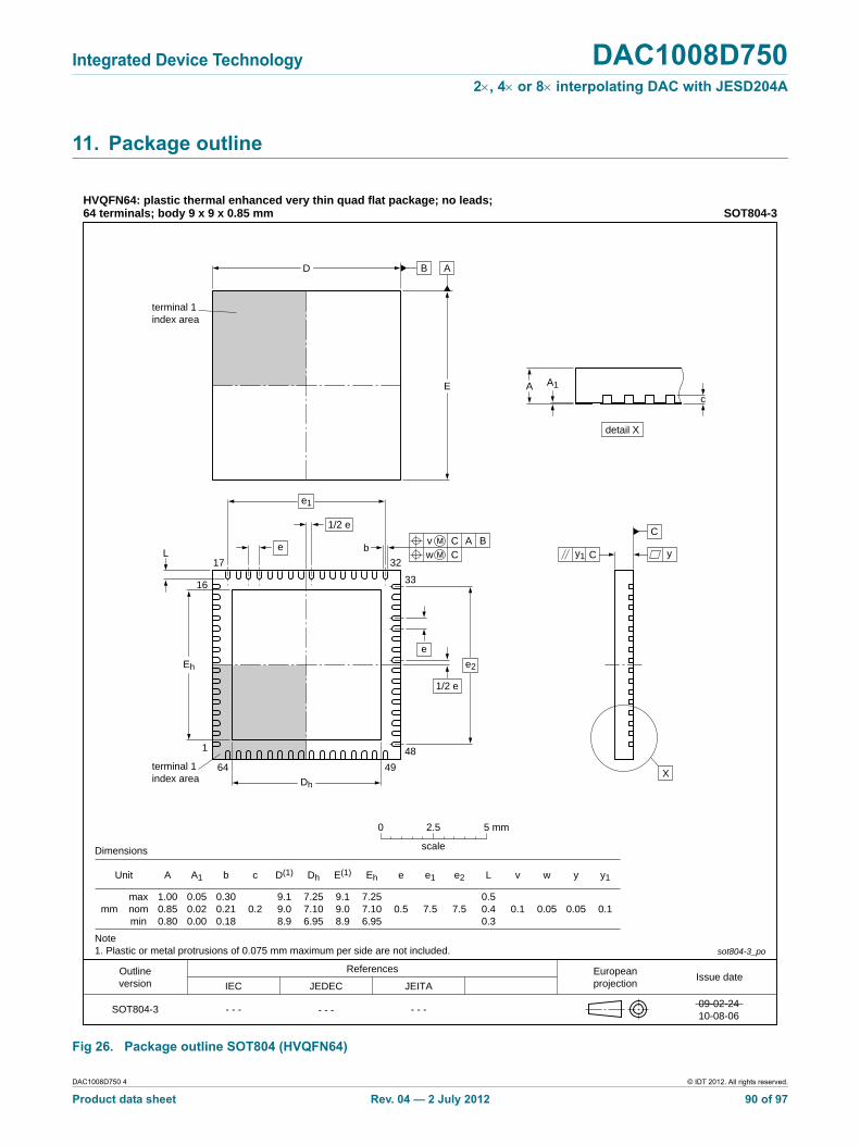
Integrated Device Technology DAC1008D7502, 4 or 8 interpolating DAC with JESD204A
11. Package outline
Fig 26. Package outline SOT804 (HVQFN64)
ReferencesOutlineversion
Europeanprojection
Issue dateIEC JEDEC JEITA
SOT804-3 - - -- - -- - -
sot804-3_po
Unit
mmmaxnommin
1.000.850.80
0.050.020.00
0.300.210.18
0.29.19.08.9
9.19.08.9
0.5 0.1 0.05
A
Dimensions
Note1. Plastic or metal protrusions of 0.075 mm maximum per side are not included.
HVQFN64: plastic thermal enhanced very thin quad flat package; no leads;64 terminals; body 9 x 9 x 0.85 mm SOT804-3
A1 b c D(1)
0.1
y1Dh
7.257.106.95
E(1) Eh
7.257.106.95
e e1
7.5
e2
7.5
L
0.50.40.3
v w
0.05
y
0 2.5 5 mm
scale
terminal 1index area
terminal 1index area
BD A
E
b
e1
eAC Bv
Cw17 32
e2
e
33
48
Dh
4964
Eh
L
1
16
C
yCy1
X
detail X
A1Ac
1/2 e
1/2 e
09-02-2410-08-06
DAC1008D750 4 © IDT 2012. All rights reserved.
Product data sheet Rev. 04 — 2 July 2012 90 of 97
Integrated Device Technology DAC1008D7502, 4 or 8 interpolating DAC with JESD204A
12. Abbreviations
Table 203. Abbreviations
Acronym Description
AQM Analog Quadrature Modulator
BER Bit Error Rate
BW BandWidth
CDI Clock Domain Interface
CDMA Code Division Multiple Access
CML Current Mode Logic
CMOS Complementary Metal Oxide Semiconductor
DAC Digital-to-Analog Converter
DCSMU Device Configuration Management and Start-up Unit
DES DESerializer
EDGE Enhanced Data rates for GSM Evolution
FIR Finite Impulse Response
FPGA Field Programmable Gate Array
GSM Global System for Mobile communications
IF Intermediate Frequency
ILA Inter-Lane Alignment
IMD3 third order InterMoDulation product
LMDS Local Multipoint Distribution Service
LSB Least Significant Bit
LTE Long Term Evolution
LVDS Low-Voltage Differential Signaling
MDS Multipoint Distribution Service
MMDS Multichannel Multipoint Distribution Service
MSB Most Significant Bit
NCO Numerically Controlled Oscillator
NMOS Negative Metal-Oxide Semiconductor
PLL Phase-Locked Loop
SERDES SERializer/DESerializer
SFDR Spurious Free Dynamic Range
SPI Serial Peripheral Interface
TD-SCDMA Time Division-Synchronous Code Division Multiple Access
WCDMA Wideband Code Division Multiple Access
WiMax Worldwide interoperability for Microwave Access
DAC1008D750 4 © IDT 2012. All rights reserved.
Product data sheet Rev. 04 — 2 July 2012 91 of 97
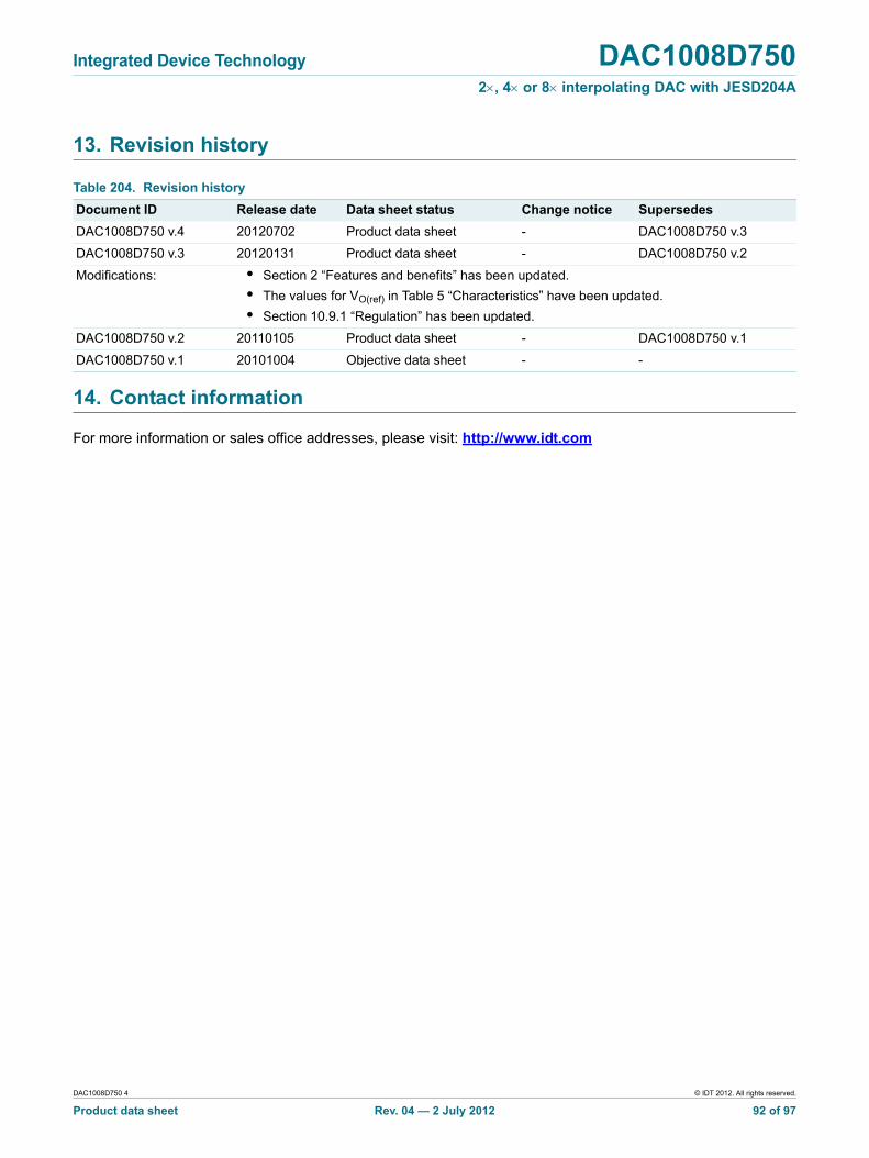
Integrated Device Technology DAC1008D7502, 4 or 8 interpolating DAC with JESD204A
13. Revision history
14. Contact information
For more information or sales office addresses, please visit: http://www.idt.com
Table 204. Revision history
Document ID Release date Data sheet status Change notice Supersedes
DAC1008D750 v.4 20120702 Product data sheet - DAC1008D750 v.3
DAC1008D750 v.3 20120131 Product data sheet - DAC1008D750 v.2
Modifications: • Section 2 “Features and benefits” has been updated.
• The values for VO(ref) in Table 5 “Characteristics” have been updated.
• Section 10.9.1 “Regulation” has been updated.
DAC1008D750 v.2 20110105 Product data sheet - DAC1008D750 v.1
DAC1008D750 v.1 20101004 Objective data sheet - -
DAC1008D750 4 © IDT 2012. All rights reserved.
Product data sheet Rev. 04 — 2 July 2012 92 of 97
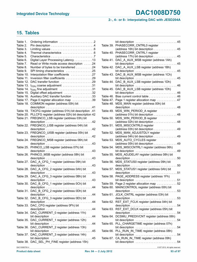
Integrated Device Technology DAC1008D7502, 4 or 8 interpolating DAC with JESD204A
15. Tables
Table 1. Ordering information . . . . . . . . . . . . . . . . . . . . .2Table 2. Pin description . . . . . . . . . . . . . . . . . . . . . . . . . .4Table 3. Limiting values . . . . . . . . . . . . . . . . . . . . . . . . . .6Table 4. Thermal characteristics . . . . . . . . . . . . . . . . . . .6Table 5. Characteristics . . . . . . . . . . . . . . . . . . . . . . . . . .7Table 6. Digital Layer Processing Latency . . . . . . . . . . .13Table 7. Read or Write mode access description . . . . .24Table 8. Number of bytes to be transferred . . . . . . . . . .24Table 9. SPI timing characteristics . . . . . . . . . . . . . . . .25Table 10. Interpolation filter coefficients . . . . . . . . . . . . .27Table 11. Inversion filter coefficients . . . . . . . . . . . . . . . .29Table 12. DAC transfer function . . . . . . . . . . . . . . . . . . .29Table 13. IO(fs) coarse adjustment . . . . . . . . . . . . . . . . . .31Table 14. IO(fs) fine adjustment . . . . . . . . . . . . . . . . . . . .31Table 15. Digital offset adjustment . . . . . . . . . . . . . . . . .32Table 16. Auxiliary DAC transfer function . . . . . . . . . . . .33Table 17. Page 0 register allocation map . . . . . . . . . . . .39Table 18. COMMON register (address 00h) bit
description . . . . . . . . . . . . . . . . . . . . . . . . . . . .41Table 19. TXCFG register (address 01h) bit description .41Table 20. PLLCFG register (address 02h) bit description 42Table 21. FREQNCO_LSB register (address 03h) bit
description . . . . . . . . . . . . . . . . . . . . . . . . . . . .42Table 22. FREQNCO_LISB register (address 04h) bit
description . . . . . . . . . . . . . . . . . . . . . . . . . . . .42Table 23. FREQNCO_UISB register (address 05h) bit
description . . . . . . . . . . . . . . . . . . . . . . . . . . . .42Table 24. FREQNCO_MSB register (address 06h) bit
description . . . . . . . . . . . . . . . . . . . . . . . . . . . .43Table 25. PHINCO_LSB register (address 07h) bit
description . . . . . . . . . . . . . . . . . . . . . . . . . . . .43Table 26. PHINCO_MSB register (address 08h) bit
description . . . . . . . . . . . . . . . . . . . . . . . . . . . .43Table 27. DAC_A_CFG_1 register (address 09h) bit
description . . . . . . . . . . . . . . . . . . . . . . . . . . . .43Table 28. DAC_A_CFG_2 register (address 0Ah) bit
description . . . . . . . . . . . . . . . . . . . . . . . . . . . .43Table 29. DAC_A_CFG_3 register (address 0Bh) bit
description . . . . . . . . . . . . . . . . . . . . . . . . . . . .43Table 30. DAC_B_CFG_1 register (address 0Ch) bit
description . . . . . . . . . . . . . . . . . . . . . . . . . . . .44Table 31. DAC_B_CFG_2 register (address 0Dh) bit
description . . . . . . . . . . . . . . . . . . . . . . . . . . . .44Table 32. DAC_B_CFG_3 register (address 0Eh) bit
description . . . . . . . . . . . . . . . . . . . . . . . . . . . .44Table 33. DAC_CFG register (address 0Fh) bit
description . . . . . . . . . . . . . . . . . . . . . . . . . . . .44Table 34. DAC_CURRENT_0 register (address 11h)
bit description . . . . . . . . . . . . . . . . . . . . . . . . .44Table 35. DAC_CURRENT_1 register (address 12h)
bit description . . . . . . . . . . . . . . . . . . . . . . . . .44Table 36. DAC_CURRENT_2 register (address 13h)
bit description . . . . . . . . . . . . . . . . . . . . . . . . .45Table 37. DAC_CURRENT_3 register (address 14h)
bit description . . . . . . . . . . . . . . . . . . . . . . . . .45Table 38. DAC_SEL_PH_FINE register (address 15h)
bit description . . . . . . . . . . . . . . . . . . . . . . . . . 45Table 39. PHASECORR_CNTRL0 register
(address 16h) bit description . . . . . . . . . . . . . . 45Table 40. PHASECORR_CNTRL1 register
(address 17h) bit description . . . . . . . . . . . . . . 45Table 41. DAC_A_AUX_MSB register (address 1Ah)
bit description . . . . . . . . . . . . . . . . . . . . . . . . . 45Table 42. DAC_A_AUX_LSB register (address 1Bh)
bit description . . . . . . . . . . . . . . . . . . . . . . . . . 45Table 43. DAC_B_AUX_MSB register (address 1Ch)
bit description . . . . . . . . . . . . . . . . . . . . . . . . . 45Table 44. DAC_B_AUX_LSB register (address 1Dh)
bit description . . . . . . . . . . . . . . . . . . . . . . . . . 46Table 45. DAC_B_AUX_LSB register (address 1Dh)
bit description . . . . . . . . . . . . . . . . . . . . . . . . . 46Table 46. Bias current control table . . . . . . . . . . . . . . . . . 46Table 47. Page 1 register allocation map . . . . . . . . . . . . 47Table 48. MDS_MAIN register (address 00h) bit
description . . . . . . . . . . . . . . . . . . . . . . . . . . . . 48Table 49. MDS_WIN_PERIOD_A register
(address 01h) bit description . . . . . . . . . . . . . . 48Table 50. MDS_WIN_PERIOD_B register
(address 02h) bit description . . . . . . . . . . . . . . 48Table 51. MDS_MISCCNTRL0 register
(address 03h) bit description . . . . . . . . . . . . . . 49Table 52. MDS_MAN_ADJUSTDLY register
(address 04h) bit description . . . . . . . . . . . . . . 49Table 53. MDS_AUTO_CYCLES register
(address 05h) bit description . . . . . . . . . . . . . . 49Table 54. MDS_MISCCNTRL1 register (address 06h)
bit description . . . . . . . . . . . . . . . . . . . . . . . . . 49Table 55. MDS_ADJDELAY register (address 08h) bit
description . . . . . . . . . . . . . . . . . . . . . . . . . . . . 50Table 56. MDS_STATUS0 register (address 09h) bit
description . . . . . . . . . . . . . . . . . . . . . . . . . . . . 50Table 57. MDS_STATUS1 register (address 0Ah) bit
description . . . . . . . . . . . . . . . . . . . . . . . . . . . . 51Table 58. PAGE_ADDRESS register (address 1Fh)
bit description . . . . . . . . . . . . . . . . . . . . . . . . . 51Table 59. Page 2 register allocation map . . . . . . . . . . . . 52Table 60. MAINCONTROL register (address 00h) bit
description . . . . . . . . . . . . . . . . . . . . . . . . . . . . 53Table 61. JCLK_CNTRL register (address 03h) bit
description . . . . . . . . . . . . . . . . . . . . . . . . . . . . 53Table 62. RST_EXT_FCLK register (address 04h) bit
description . . . . . . . . . . . . . . . . . . . . . . . . . . . . 54Table 63. RST_EXT_DCLK register (address 05h) bit
description . . . . . . . . . . . . . . . . . . . . . . . . . . . . 54Table 64. DCSMU_PREDIVCNT register (address 06h)
bit description . . . . . . . . . . . . . . . . . . . . . . . . . 54Table 65. PLL_CHARGETIME register (address 07h)
bit description . . . . . . . . . . . . . . . . . . . . . . . . . 54Table 66. PLL_RUN_IN_TIME register (address 08h)
bit description . . . . . . . . . . . . . . . . . . . . . . . . . 54Table 67. CA_RUN_IN_TIME register (address 09h)
bit description . . . . . . . . . . . . . . . . . . . . . . . . . 54
DAC1008D750 4 © IDT 2012. All rights reserved.
Product data sheet Rev. 04 — 2 July 2012 93 of 97
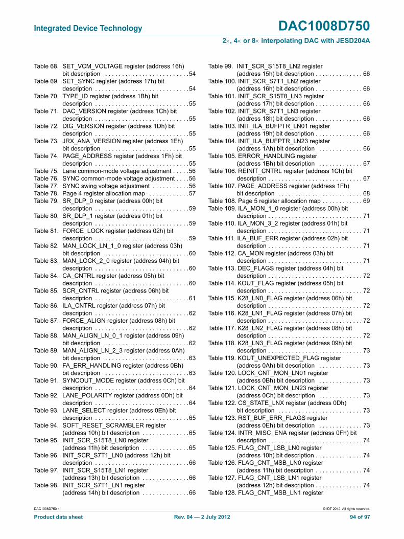
Integrated Device Technology DAC1008D7502, 4 or 8 interpolating DAC with JESD204A
Table 68. SET_VCM_VOLTAGE register (address 16h) bit description . . . . . . . . . . . . . . . . . . . . . . . . .54
Table 69. SET_SYNC register (address 17h) bit description . . . . . . . . . . . . . . . . . . . . . . . . . . . .54
Table 70. TYPE_ID register (address 1Bh) bit description . . . . . . . . . . . . . . . . . . . . . . . . . . . .55
Table 71. DAC_VERSION register (address 1Ch) bit description . . . . . . . . . . . . . . . . . . . . . . . . . . . .55
Table 72. DIG_VERSION register (address 1Dh) bit description . . . . . . . . . . . . . . . . . . . . . . . . . . . .55
Table 73. JRX_ANA_VERSION register (address 1Eh) bit description . . . . . . . . . . . . . . . . . . . . . . . . .55
Table 74. PAGE_ADDRESS register (address 1Fh) bit description . . . . . . . . . . . . . . . . . . . . . . . . . . . .55
Table 75. Lane common-mode voltage adjustment . . . . .56Table 76. SYNC common-mode voltage adjustment . . . .56Table 77. SYNC swing voltage adjustment . . . . . . . . . . .56Table 78. Page 4 register allocation map . . . . . . . . . . . .57Table 79. SR_DLP_0 register (address 00h) bit
description . . . . . . . . . . . . . . . . . . . . . . . . . . . .59Table 80. SR_DLP_1 register (address 01h) bit
description . . . . . . . . . . . . . . . . . . . . . . . . . . . .59Table 81. FORCE_LOCK register (address 02h) bit
description . . . . . . . . . . . . . . . . . . . . . . . . . . . .59Table 82. MAN_LOCK_LN_1_0 register (address 03h)
bit description . . . . . . . . . . . . . . . . . . . . . . . . .60Table 83. MAN_LOCK_2_0 register (address 04h) bit
description . . . . . . . . . . . . . . . . . . . . . . . . . . . .60Table 84. CA_CNTRL register (address 05h) bit
description . . . . . . . . . . . . . . . . . . . . . . . . . . . .60Table 85. SCR_CNTRL register (address 06h) bit
description . . . . . . . . . . . . . . . . . . . . . . . . . . . .61Table 86. ILA_CNTRL register (address 07h) bit
description . . . . . . . . . . . . . . . . . . . . . . . . . . . .62Table 87. FORCE_ALIGN register (address 08h) bit
description . . . . . . . . . . . . . . . . . . . . . . . . . . . .62Table 88. MAN_ALIGN_LN_0_1 register (address 09h)
bit description . . . . . . . . . . . . . . . . . . . . . . . . .62Table 89. MAN_ALIGN_LN_2_3 register (address 0Ah)
bit description . . . . . . . . . . . . . . . . . . . . . . . . .63Table 90. FA_ERR_HANDLING register (address 0Bh)
bit description . . . . . . . . . . . . . . . . . . . . . . . . .63Table 91. SYNCOUT_MODE register (address 0Ch) bit
description . . . . . . . . . . . . . . . . . . . . . . . . . . . .64Table 92. LANE_POLARITY register (address 0Dh) bit
description . . . . . . . . . . . . . . . . . . . . . . . . . . . .64Table 93. LANE_SELECT register (address 0Eh) bit
description . . . . . . . . . . . . . . . . . . . . . . . . . . . .65Table 94. SOFT_RESET_SCRAMBLER register
(address 10h) bit description . . . . . . . . . . . . . .65Table 95. INIT_SCR_S15T8_LN0 register
(address 11h) bit description . . . . . . . . . . . . . .65Table 96. INIT_SCR_S7T1_LN0 (address 12h) bit
description . . . . . . . . . . . . . . . . . . . . . . . . . . . .66Table 97. INIT_SCR_S15T8_LN1 register
(address 13h) bit description . . . . . . . . . . . . . .66Table 98. INIT_SCR_S7T1_LN1 register
(address 14h) bit description . . . . . . . . . . . . . .66
Table 99. INIT_SCR_S15T8_LN2 register (address 15h) bit description . . . . . . . . . . . . . . 66
Table 100. INIT_SCR_S7T1_LN2 register (address 16h) bit description . . . . . . . . . . . . . . 66
Table 101. INIT_SCR_S15T8_LN3 register (address 17h) bit description . . . . . . . . . . . . . . 66
Table 102. INIT_SCR_S7T1_LN3 register (address 18h) bit description . . . . . . . . . . . . . . 66
Table 103. INIT_ILA_BUFPTR_LN01 register (address 19h) bit description . . . . . . . . . . . . . . 66
Table 104. INIT_ILA_BUFPTR_LN23 register (address 1Ah) bit description . . . . . . . . . . . . . 66
Table 105. ERROR_HANDLING register (address 1Bh) bit description . . . . . . . . . . . . . 67
Table 106. REINIT_CNTRL register (address 1Ch) bit description . . . . . . . . . . . . . . . . . . . . . . . . . . . . 67
Table 107. PAGE_ADDRESS register (address 1Fh) bit description . . . . . . . . . . . . . . . . . . . . . . . . . 68
Table 108. Page 5 register allocation map . . . . . . . . . . . . 69Table 109. ILA_MON_1_0 register (address 00h) bit
description . . . . . . . . . . . . . . . . . . . . . . . . . . . . 71Table 110. ILA_MON_3_2 register (address 01h) bit
description . . . . . . . . . . . . . . . . . . . . . . . . . . . . 71Table 111. ILA_BUF_ERR register (address 02h) bit
description . . . . . . . . . . . . . . . . . . . . . . . . . . . . 71Table 112. CA_MON register (address 03h) bit
description . . . . . . . . . . . . . . . . . . . . . . . . . . . . 71Table 113. DEC_FLAGS register (address 04h) bit
description . . . . . . . . . . . . . . . . . . . . . . . . . . . . 72Table 114. KOUT_FLAG register (address 05h) bit
description . . . . . . . . . . . . . . . . . . . . . . . . . . . . 72Table 115. K28_LN0_FLAG register (address 06h) bit
description . . . . . . . . . . . . . . . . . . . . . . . . . . . . 72Table 116. K28_LN1_FLAG register (address 07h) bit
description . . . . . . . . . . . . . . . . . . . . . . . . . . . . 72Table 117. K28_LN2_FLAG register (address 08h) bit
description . . . . . . . . . . . . . . . . . . . . . . . . . . . . 72Table 118. K28_LN3_FLAG register (address 09h) bit
description . . . . . . . . . . . . . . . . . . . . . . . . . . . . 73Table 119. KOUT_UNEXPECTED_FLAG register
(address 0Ah) bit description . . . . . . . . . . . . . 73Table 120. LOCK_CNT_MON_LN01 register
(address 0Bh) bit description . . . . . . . . . . . . . 73Table 121. LOCK_CNT_MON_LN23 register
(address 0Ch) bit description . . . . . . . . . . . . . 73Table 122. CS_STATE_LNX register (address 0Dh)
bit description . . . . . . . . . . . . . . . . . . . . . . . . . 73Table 123. RST_BUF_ERR_FLAGS register
(address 0Eh) bit description . . . . . . . . . . . . . 73Table 124. INTR_MISC_ENA register (address 0Fh) bit
description . . . . . . . . . . . . . . . . . . . . . . . . . . . . 74Table 125. FLAG_CNT_LSB_LN0 register
(address 10h) bit description . . . . . . . . . . . . . . 74Table 126. FLAG_CNT_MSB_LN0 register
(address 11h) bit description . . . . . . . . . . . . . . 74Table 127. FLAG_CNT_LSB_LN1 register
(address 12h) bit description . . . . . . . . . . . . . . 74Table 128. FLAG_CNT_MSB_LN1 register
DAC1008D750 4 © IDT 2012. All rights reserved.
Product data sheet Rev. 04 — 2 July 2012 94 of 97
Integrated Device Technology DAC1008D7502, 4 or 8 interpolating DAC with JESD204A
(address 13h) bit description . . . . . . . . . . . . . .74Table 129. FLAG_CNT_LSB_LN2 register
(address 14h) bit description . . . . . . . . . . . . . .74Table 130. FLAG_CNT_MSB_LN2 register
(address 15h) bit description . . . . . . . . . . . . . .74Table 131. FLAG_CNT_LSB_LN3 register
(address 16h) bit description . . . . . . . . . . . . . .74Table 132. FLAG_CNT_MSB_LN3 register
(address 17h) bit description . . . . . . . . . . . . . .75Table 133. BER_LEVEL_LSB register (address 18h)
bit description . . . . . . . . . . . . . . . . . . . . . . . . .75Table 134. BER_LEVEL_MSB register (address 19h)
bit description . . . . . . . . . . . . . . . . . . . . . . . . . .75Table 135. INTR_ENA register (address 1Ah) bit
description . . . . . . . . . . . . . . . . . . . . . . . . . . . .75Table 136. CNTRL_FLAGCNT_LN01 register
(address 1Bh) bit description . . . . . . . . . . . . . .76Table 137. CNTRL_FLAGCNT_LN23 register
(address 1Ch) bit description . . . . . . . . . . . . . .76Table 138. MON_FLAGS_RESET register
(address 1Dh) bit description . . . . . . . . . . . . . .76Table 139. DBG_CNTRL register (address 1Eh) bit
description . . . . . . . . . . . . . . . . . . . . . . . . . . . .77Table 140. PAGE_ADDRESS register (address 1Fh)
bit description . . . . . . . . . . . . . . . . . . . . . . . . .77Table 141. Counter source . . . . . . . . . . . . . . . . . . . . . . . .77Table 142. Code group synchronization state machine. . .77Table 143. Page 6 register allocation map . . . . . . . . . . . .78Table 144. LN0_CFG_0 register (address 00h) bit
description . . . . . . . . . . . . . . . . . . . . . . . . . . . .80Table 145. LN0_CFG_1 register (address 01h) bit
description . . . . . . . . . . . . . . . . . . . . . . . . . . . .80Table 146. LN0_CFG_2 register (address 02h) bit
description . . . . . . . . . . . . . . . . . . . . . . . . . . . .80Table 147. LN0_CFG_3 register (address 03h) bit
description . . . . . . . . . . . . . . . . . . . . . . . . . . . .80Table 148. LN0_CFG_4 register (address 04h) bit
description . . . . . . . . . . . . . . . . . . . . . . . . . . . .80Table 149. LN0_CFG_5 register (address 05h) bit
description . . . . . . . . . . . . . . . . . . . . . . . . . . . .80Table 150. LN0_CFG_6 register (address 06h) bit
description . . . . . . . . . . . . . . . . . . . . . . . . . . . .80Table 151. LN0_CFG_7 register (address 07h) bit
description . . . . . . . . . . . . . . . . . . . . . . . . . . . .80Table 152. LN0_CFG_8 register (address 08h) bit
description . . . . . . . . . . . . . . . . . . . . . . . . . . . .81Table 153. LN0_CFG_9 register (address 09h) bit
description . . . . . . . . . . . . . . . . . . . . . . . . . . . .81Table 154. LN0_CFG_10 register (address 0Ah) bit
description . . . . . . . . . . . . . . . . . . . . . . . . . . . .81Table 155. LN0_CFG_11 register (address 0Bh) bit
description . . . . . . . . . . . . . . . . . . . . . . . . . . . .81Table 156. LN0_CFG_12 register (address 0Ch) bit
description . . . . . . . . . . . . . . . . . . . . . . . . . . . .81Table 157. LN0_CFG_13 register (address 0Dh) bit
description . . . . . . . . . . . . . . . . . . . . . . . . . . . .81Table 158. LN1_CFG_0 register (address 10h) bit
description . . . . . . . . . . . . . . . . . . . . . . . . . . . .81
Table 159. LN1_CFG_1 register (address 11h) bit description . . . . . . . . . . . . . . . . . . . . . . . . . . . . 81
Table 160. LN1_CFG_2 register (address 12h) bit description . . . . . . . . . . . . . . . . . . . . . . . . . . . . 81
Table 161. LN1_CFG_3 register (address 13h) bit description . . . . . . . . . . . . . . . . . . . . . . . . . . . . 82
Table 162. LN1_CFG_4 register (address 14h) bit description . . . . . . . . . . . . . . . . . . . . . . . . . . . . 82
Table 163. LN1_CFG_5 register (address 15h) bit description . . . . . . . . . . . . . . . . . . . . . . . . . . . . 82
Table 164. LN1_CFG_6 register (address 16h) bit description . . . . . . . . . . . . . . . . . . . . . . . . . . . . 82
Table 165. LN1_CFG_7 register (address 17h) bit description . . . . . . . . . . . . . . . . . . . . . . . . . . . . 82
Table 166. LN1_CFG_8 register (address 18h) bit description . . . . . . . . . . . . . . . . . . . . . . . . . . . . 82
Table 167. LN1_CFG_9 register (address 19h) bit description . . . . . . . . . . . . . . . . . . . . . . . . . . . . 82
Table 168. LN1_CFG_10 register (address 1Ah) bit description . . . . . . . . . . . . . . . . . . . . . . . . . . . . 82
Table 169. LN1_CFG_11 register (address 1Bh) bit description . . . . . . . . . . . . . . . . . . . . . . . . . . . . 83
Table 170. LN1_CFG_12 register (address 1Ch) bit description . . . . . . . . . . . . . . . . . . . . . . . . . . . . 83
Table 171. LN1_CFG_13 register (address 1Dh) bit description . . . . . . . . . . . . . . . . . . . . . . . . . . . . 83
Table 172. PAGE_ADDRESS register (address 1Fh) bit description . . . . . . . . . . . . . . . . . . . . . . . . . 83
Table 173. Page 7 register allocation map . . . . . . . . . . . . 84Table 174. LN2_CFG_0 register (address 00h) bit
description . . . . . . . . . . . . . . . . . . . . . . . . . . . . 86Table 175. LN2_CFG_1 register (address 01h) bit
description . . . . . . . . . . . . . . . . . . . . . . . . . . . . 86Table 176. LN2_CFG_2 register (address 02h) bit
description . . . . . . . . . . . . . . . . . . . . . . . . . . . . 86Table 177. LN2_CFG_3 register (address 03h) bit
description . . . . . . . . . . . . . . . . . . . . . . . . . . . . 86Table 178. LN2_CFG_4 register (address 04h) bit
description . . . . . . . . . . . . . . . . . . . . . . . . . . . . 86Table 179. LN2_CFG_5 register (address 05h) bit
description . . . . . . . . . . . . . . . . . . . . . . . . . . . . 86Table 180. LN2_CFG_6 register (address 06h) bit
description . . . . . . . . . . . . . . . . . . . . . . . . . . . . 86Table 181. LN2_CFG_7 register (address 07h) bit
description . . . . . . . . . . . . . . . . . . . . . . . . . . . . 86Table 182. LN2_CFG_8 register (address 08h) bit
description . . . . . . . . . . . . . . . . . . . . . . . . . . . . 87Table 183. LN2_CFG_9 register (address 09h) bit
description . . . . . . . . . . . . . . . . . . . . . . . . . . . . 87Table 184. LN2_CFG_10 register (address 0Ah) bit
description . . . . . . . . . . . . . . . . . . . . . . . . . . . . 87Table 185. LN2_CFG_11 register (address 0Bh) bit
description . . . . . . . . . . . . . . . . . . . . . . . . . . . . 87Table 186. LN2_CFG_12 register (address 0Ch) bit
description . . . . . . . . . . . . . . . . . . . . . . . . . . . . 87Table 187. LN2_CFG_13 register (address 0Dh) bit
description . . . . . . . . . . . . . . . . . . . . . . . . . . . . 87Table 188. LN3_CFG_0 register (address 10h) bit
DAC1008D750 4 © IDT 2012. All rights reserved.
Product data sheet Rev. 04 — 2 July 2012 95 of 97
Integrated Device Technology DAC1008D7502, 4 or 8 interpolating DAC with JESD204A
description . . . . . . . . . . . . . . . . . . . . . . . . . . . .87Table 189. LN3_CFG_1 register (address 11h) bit
description . . . . . . . . . . . . . . . . . . . . . . . . . . . .87Table 190. LN3_CFG_2 register (address 12h) bit
description . . . . . . . . . . . . . . . . . . . . . . . . . . . .87Table 191. LN3_CFG_3 register (address 13h) bit
description . . . . . . . . . . . . . . . . . . . . . . . . . . . .88Table 192. LN3_CFG_4 register (address 14h) bit
description . . . . . . . . . . . . . . . . . . . . . . . . . . . .88Table 193. LN3_CFG_5 register (address 15h) bit
description . . . . . . . . . . . . . . . . . . . . . . . . . . . .88Table 194. LN3_CFG_6 register (address 16h) bit
description . . . . . . . . . . . . . . . . . . . . . . . . . . . .88Table 195. LN3_CFG_7 register (address 17h) bit
description . . . . . . . . . . . . . . . . . . . . . . . . . . . .88Table 196. LN3_CFG_8 register (address 18h) bit
description . . . . . . . . . . . . . . . . . . . . . . . . . . . .88Table 197. LN3_CFG_9 register (address 19h) bit
description . . . . . . . . . . . . . . . . . . . . . . . . . . . .88Table 198. LN3_CFG_10 register (address 1Ah) bit
description . . . . . . . . . . . . . . . . . . . . . . . . . . . .88Table 199. LN3_CFG_11 register (address 1Bh) bit
description . . . . . . . . . . . . . . . . . . . . . . . . . . . .89Table 200. LN3_CFG_12 register (address 1Ch) bit
description . . . . . . . . . . . . . . . . . . . . . . . . . . . .89Table 201. LN3_CFG_13 register (address 1Dh) bit
description . . . . . . . . . . . . . . . . . . . . . . . . . . . .89Table 202. PAGE_ADDRESS register (address 1Fh)
bit description . . . . . . . . . . . . . . . . . . . . . . . . .89Table 203. Abbreviations . . . . . . . . . . . . . . . . . . . . . . . . .91Table 204. Revision history . . . . . . . . . . . . . . . . . . . . . . . .92
DAC1008D750 4 © IDT 2012. All rights reserved.
Product data sheet Rev. 04 — 2 July 2012 96 of 97
Integrated Device Technology DAC1008D7502, 4 or 8 interpolating DAC with JESD204A
16. Contents
1 General description . . . . . . . . . . . . . . . . . . . . . . 1
2 Features and benefits . . . . . . . . . . . . . . . . . . . . 1
3 Applications . . . . . . . . . . . . . . . . . . . . . . . . . . . . 2
4 Ordering information. . . . . . . . . . . . . . . . . . . . . 2
5 Block diagram . . . . . . . . . . . . . . . . . . . . . . . . . . 3
6 Pinning information. . . . . . . . . . . . . . . . . . . . . . 46.1 Pinning . . . . . . . . . . . . . . . . . . . . . . . . . . . . . . . 46.2 Pin description . . . . . . . . . . . . . . . . . . . . . . . . . 4
7 Limiting values. . . . . . . . . . . . . . . . . . . . . . . . . . 6
8 Thermal characteristics . . . . . . . . . . . . . . . . . . 6
9 Characteristics. . . . . . . . . . . . . . . . . . . . . . . . . . 7
10 Application information. . . . . . . . . . . . . . . . . . 1210.1 General description . . . . . . . . . . . . . . . . . . . . 1210.2 JESD204A receiver . . . . . . . . . . . . . . . . . . . . 1310.2.1 Lane input . . . . . . . . . . . . . . . . . . . . . . . . . . . . 1410.2.2 Sync and word align . . . . . . . . . . . . . . . . . . . . 1410.2.3 Comma detection and word align . . . . . . . . . . 1510.2.4 Descrambler . . . . . . . . . . . . . . . . . . . . . . . . . . 1610.2.5 Inter-lane alignment . . . . . . . . . . . . . . . . . . . . 1610.2.5.1 Single device operation . . . . . . . . . . . . . . . . . 1610.2.5.2 Multi-device operation . . . . . . . . . . . . . . . . . . 1610.2.5.3 Master/slave mode . . . . . . . . . . . . . . . . . . . . . 1810.2.5.4 All slave mode . . . . . . . . . . . . . . . . . . . . . . . . 2110.2.6 Frame assembly . . . . . . . . . . . . . . . . . . . . . . . 2210.3 Serial Peripheral Interface (SPI) . . . . . . . . . . . 2410.3.1 Protocol description . . . . . . . . . . . . . . . . . . . . 2410.3.2 SPI timing description. . . . . . . . . . . . . . . . . . . 2510.4 Clock input . . . . . . . . . . . . . . . . . . . . . . . . . . . 2610.5 FIR filters . . . . . . . . . . . . . . . . . . . . . . . . . . . . 2710.6 Quadrature modulator and Numerically
Controlled Oscillator (NCO) . . . . . . . . . . . . . . 2810.6.1 NCO in 32-bit . . . . . . . . . . . . . . . . . . . . . . . . . 2810.6.2 Low-power NCO . . . . . . . . . . . . . . . . . . . . . . . 2810.6.3 Minus_3dB . . . . . . . . . . . . . . . . . . . . . . . . . . . 2810.7 x / (sin x) . . . . . . . . . . . . . . . . . . . . . . . . . . . . . 2810.8 DAC transfer function . . . . . . . . . . . . . . . . . . . 2910.9 Full-scale current . . . . . . . . . . . . . . . . . . . . . . 3010.9.1 Regulation . . . . . . . . . . . . . . . . . . . . . . . . . . . 3010.9.1.1 External regulation . . . . . . . . . . . . . . . . . . . . . 3010.9.2 Full-scale current adjustment . . . . . . . . . . . . . 3010.10 Digital offset correction . . . . . . . . . . . . . . . . . . 3110.11 Analog output . . . . . . . . . . . . . . . . . . . . . . . . . 3210.12 Auxiliary DACs . . . . . . . . . . . . . . . . . . . . . . . . 3310.13 Output configuration . . . . . . . . . . . . . . . . . . . . 3410.13.1 Basic output configuration . . . . . . . . . . . . . . . 3410.13.2 DC interface to an Analog Quadrature
Modulator (AQM) . . . . . . . . . . . . . . . . . . . . . . 3510.13.3 AC interface to an Analog Quadrature
Modulator (AQM) . . . . . . . . . . . . . . . . . . . . . . 3710.13.4 Phase correction. . . . . . . . . . . . . . . . . . . . . . . 3810.14 Power and grounding . . . . . . . . . . . . . . . . . . . 3810.15 Configuration interface . . . . . . . . . . . . . . . . . . 3810.15.1 Register description . . . . . . . . . . . . . . . . . . . . 3810.15.2 Detailed descriptions of registers . . . . . . . . . . 38
10.15.2.1 Page 0 allocation map description . . . . . . . . . 3910.15.2.2 Page 0 bit definition detailed description . . . . 4110.15.2.3 Page 1 allocation map description . . . . . . . . . 4710.15.2.4 Page 1 bit definition detailed description . . . . 4810.15.2.5 Page 2 allocation map description . . . . . . . . . 5210.15.2.6 Page 2 bit definition detailed description . . . . 5310.15.2.7 Page 4 allocation map description . . . . . . . . . 5710.15.2.8 Page 4 bit definition detailed description . . . . 5910.15.2.9 Page 5 allocation map description . . . . . . . . . 6910.15.2.10 Page 5 bit definition detailed description . . . 7110.15.2.11 Page 6 allocation map description . . . . . . . . 7810.15.2.12 Page 6 bit definition detailed description . . . 8010.15.2.13 Page 7 allocation map description . . . . . . . . 8410.15.2.14 Page 7 bit definition detailed description . . . 86
11 Package outline. . . . . . . . . . . . . . . . . . . . . . . . 90
12 Abbreviations . . . . . . . . . . . . . . . . . . . . . . . . . 91
13 Revision history . . . . . . . . . . . . . . . . . . . . . . . 92
14 Contact information . . . . . . . . . . . . . . . . . . . . 92
15 Tables . . . . . . . . . . . . . . . . . . . . . . . . . . . . . . . . 93
16 Contents. . . . . . . . . . . . . . . . . . . . . . . . . . . . . . 97
DAC1008D750 4 © IDT 2012. All rights reserved.
Product data sheet Rev. 04 — 2 July 2012 97 of 97
Related Documents