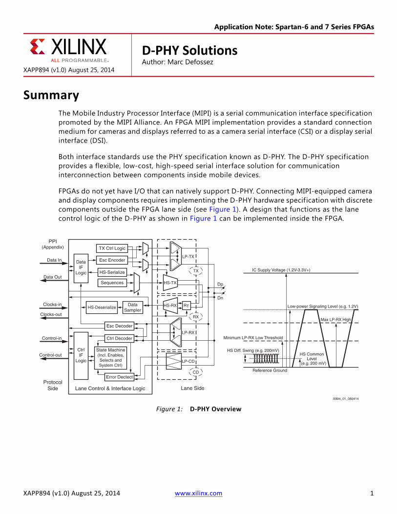
XAPP894 (v1.0) August 25, 2014 www.xilinx.com 1 Summary The Mobile Industry Processor Interface (MIPI) is a serial communication interface specification promoted by the MIPI Alliance. An FPGA MIPI implementation provides a standard connection medium for cameras and displays referred to as a camera serial interface (CSI) or a display serial interface (DSI). Both interface standards use the PHY specification known as D-PHY. The D-PHY specification provides a flexible, low-cost, high-speed serial interface solution for communication interconnection between components inside mobile devices. FPGAs do not yet have I/O that can natively support D-PHY. Connecting MIPI-equipped camera and display components requires implementing the D-PHY hardware specification with discrete components outside the FPGA lane side (see Figure 1). A design that functions as the lane control logic of the D-PHY as shown in Figure 1 can be implemented inside the FPGA. Application Note: Spartan-6 and 7 Series FPGAs XAPP894 (v1.0) August 25, 2014 D-PHY Solutions Author: Marc Defossez X-Ref Target - Figure 1 Figure 1: D-PHY Overview TX Ctrl Logic Lane Control & Interface Logic Protocol Side PPI (Appendix) Lane Side Esc Encoder HS-Serialize Data IF Logic Data In Clocks-in Data Out Control-in Control-out Clocks-out Ctrl IF Logic Sequences Esc Decoder Ctrl Decoder Error Dectect HS-Deserialize State Machine (Incl. Enables, Selects and System Ctrl) Data Sampler HS-TX IC Supply Voltage (1.2V-3.3V+) X894_01_080414 Low-power Signaling Level (e.g. 1.2V) Reference Ground HS Diff. Swing (e.g. 200mV) Minimum LP-RX Low Threshold HS Common Level (e.g. 200 mV) Max LP-RX High LP-TX LP-RX LP-CD TX Dp Dn RX CD HS-RX R T

Welcome message from author
This document is posted to help you gain knowledge. Please leave a comment to let me know what you think about it! Share it to your friends and learn new things together.
Transcript
XAPP894 (v1.0) August 25, 2014 www.xilinx.com 1
SummaryThe Mobile Industry Processor Interface (MIPI) is a serial communication interface specification promoted by the MIPI Alliance. An FPGA MIPI implementation provides a standard connection medium for cameras and displays referred to as a camera serial interface (CSI) or a display serial interface (DSI).
Both interface standards use the PHY specif ication known as D-PHY. The D-PHY specification provides a flexible, low-cost, high-speed serial interface solution for communication interconnection between components inside mobile devices.
FPGAs do not yet have I/O that can natively support D-PHY. Connecting MIPI-equipped camera and display components requires implementing the D-PHY hardware specif ication with discrete components outside the FPGA lane side (see Figure 1). A design that functions as the lane control logic of the D-PHY as shown in Figure 1 can be implemented inside the FPGA.
Application Note: Spartan-6 and 7 Series FPGAs
XAPP894 (v1.0) August 25, 2014
D-PHY SolutionsAuthor: Marc Defossez
X-Ref Target - Figure 1
Figure 1: D-PHY Overview
TX Ctrl Logic
Lane Control & Interface LogicProtocol
Side
PPI(Appendix)
Lane Side
Esc Encoder
HS-Serialize
DataIF
Logic
Data In
Clocks-in
Data Out
Control-in
Control-out
Clocks-out
CtrlIF
Logic
Sequences
Esc Decoder
Ctrl Decoder
Error Dectect
HS-Deserialize
State Machine(Incl. Enables,Selects andSystem Ctrl)
DataSampler
HS-TX
IC Supply Voltage (1.2V-3.3V+)
X894_01_080414
Low-power Signaling Level (e.g. 1.2V)
Reference Ground
HS Diff. Swing (e.g. 200mV)
Minimum LP-RX Low Threshold
HS Common Level
(e.g. 200 mV)
Max LP-RX High
LP-TX
LP-RX
LP-CD
TX
Dp
Dn
RX
CD
HS-RX RT
Introduction
XAPP894 (v1.0) August 25, 2014 www.xilinx.com 2
IntroductionThis application note provides FPGA MIPI D-PHY solutions using external hardware coupled to the standard FPGA I/O (differential and single-ended) to comply with the D-PHY version 1.00.00 14 May 2009 specif ication.
IMPORTANT: If the techniques in this application note are used for other than the application described, make sure to use the correctly qualified components.
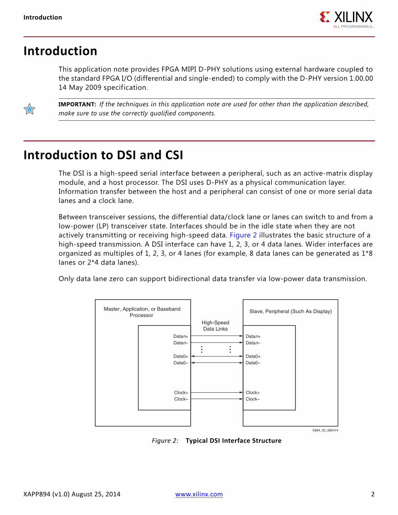
Introduction to DSI and CSIThe DSI is a high-speed serial interface between a peripheral, such as an active-matrix display module, and a host processor. The DSI uses D-PHY as a physical communication layer. Information transfer between the host and a peripheral can consist of one or more serial data lanes and a clock lane.
Between transceiver sessions, the differential data/clock lane or lanes can switch to and from a low-power (LP) transceiver state. Interfaces should be in the idle state when they are not actively transmitting or receiving high-speed data. Figure 2 illustrates the basic structure of a high-speed transmission. A DSI interface can have 1, 2, 3, or 4 data lanes. Wider interfaces are organized as multiples of 1, 2, 3, or 4 lanes (for example, 8 data lanes can be generated as 1*8 lanes or 2*4 data lanes).
Only data lane zero can support bidirectional data transfer via low-power data transmission.
X-Ref Target - Figure 2
Figure 2: Typical DSI Interface Structure
Master, Application, or BasebandProcessor
High-SpeedData Links
Datan+Datan–
Data0+Data0–
Clock+Clock–
Datan+Datan–
Data0+Data0–
Clock+Clock–
Slave, Peripheral (Such As Display)
X894_02_080414
Introduction to DSI and CSI
XAPP894 (v1.0) August 25, 2014 www.xilinx.com 3
All links between the host and the display peripheral are unidirectional, from host or master to display peripheral or slave. Only data lane zero can be bidirectional in the LP state.
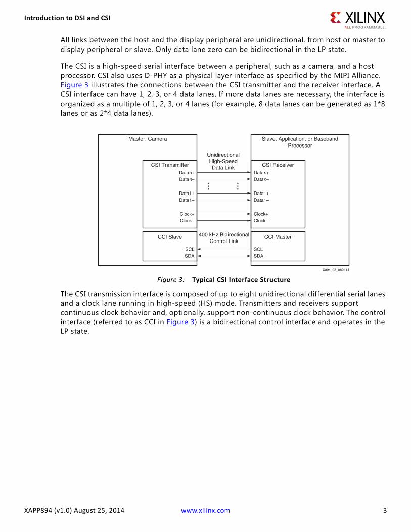
The CSI is a high-speed serial interface between a peripheral, such as a camera, and a host processor. CSI also uses D-PHY as a physical layer interface as specified by the MIPI Alliance. Figure 3 illustrates the connections between the CSI transmitter and the receiver interface. A CSI interface can have 1, 2, 3, or 4 data lanes. If more data lanes are necessary, the interface is organized as a multiple of 1, 2, 3, or 4 lanes (for example, 8 data lanes can be generated as 1*8 lanes or as 2*4 data lanes).
The CSI transmission interface is composed of up to eight unidirectional differential serial lanes and a clock lane running in high-speed (HS) mode. Transmitters and receivers support continuous clock behavior and, optionally, support non-continuous clock behavior. The control interface (referred to as CCI in Figure 3) is a bidirectional control interface and operates in the LP state.
X-Ref Target - Figure 3
Figure 3: Typical CSI Interface Structure
Master, Camera
CSI Transmitter CSI Receiver
CCI Slave CCI Master
UnidirectionalHigh-SpeedData Link
400 kHz BidirectionalControl Link
Datan+Datan–
Data1+Data1–
Clock+Clock–
Datan+Datan–
SCLSDA
SCLSDA
Data1+Data1–
Clock+Clock–
Slave, Application, or BasebandProcessor
X894_03_080414
Introduction to D-PHY
XAPP894 (v1.0) August 25, 2014 www.xilinx.com 4
Introduction to D-PHYTraditionally, interfaces between components on a printed circuit board (PCB) are based on single-ended parallel buses at low bit rates (LVCMOS), differential high-speed serial buses, or single differential channels.
The D-PHY provides an extension to this structure by turning the low-speed, low-power interface to the serial format of the high-speed differential interface, so that both are combined into a single serial interface. With this method, the D-PHY provides a flexible high-speed differential and low-speed, low-power single ended serial interface solution for interconnection between components within one product.
The D-PHY specification is written for ASSP devices or ASIC implementations in mind.
It includes and combines SLVS (high-speed) and LVCMOS (low-power) I/O into a single differential pair of wires (see Figure 1) and as previously mentioned FPGAs do not yet support native D-PHY-compliant I/O.
Because ASSP and ASIC manufacturers currently implement MIPI interfaces in their latest and most feature-rich devices, and until FPGAs have native D-PHY compliant I/O, connecting an FPGA to a MIPI aware device requires external active and/or passive components.
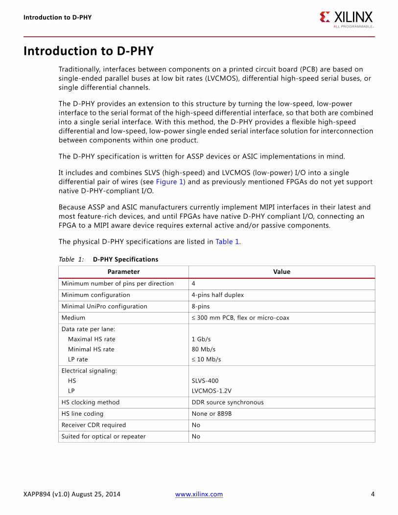
The physical D-PHY specif ications are listed in Table 1.
Table 1: D-PHY Specifications
Parameter Value
Minimum number of pins per direction 4
Minimum configuration 4-pins half duplex
Minimal UniPro configuration 8-pins
Medium ≤ 300 mm PCB, flex or micro-coax
Data rate per lane:
Maximal HS rate
Minimal HS rate
LP rate
1 Gb/s
80 Mb/s
≤ 10 Mb/s
Electrical signaling:
HS
LP
SLVS-400
LVCMOS-1.2V
HS clocking method DDR source synchronous
HS line coding None or 8B9B
Receiver CDR required No
Suited for optical or repeater No
Introduction to D-PHY
XAPP894 (v1.0) August 25, 2014 www.xilinx.com 5
The main D-PHY rules of operation are:
• Two wires as a differential pair per data lane or data link and two wires as a differential pair for the clock lane or clock link.
° Four wires comprise the minimum PHY configuration (one data lane and one clock link).
° The characteristic impedance is 100 differential, 50 single-ended per line.
• Each link has a master and a slave side.
° The master provides the high-speed DDR clock signal to the clock lane and it is the main data source.
° The slave receives the clock signal at the clock lane and is the main data sink.
° The clock lane remains in the forward direction, from master to slave.
° Bidirectional data lanes can be turned around. Source data can go from master side to slave side or from slave side to master side.
• In high-speed mode:
° Each lane is terminated and driven by a low-swing, differential signal.
° A high-speed transmitter (HS-TX) always drives the lane differentially.
° High-speed signals have a low voltage swing and a common mode of 200 mV, like SLVS.
° High-speed functions are used for high-speed data transmission only.
° High-speed functions include a differential transmitter (HS-TX) and a differential receiver (HS-RX).
• In low-power mode:
° All wires are operated single-ended and are not terminated.
° Two LP-TX outputs drive each wire of the lane independently in a single-ended configuration.
° Low-power signals have a large swing of 1.2V, LVCMOS_12 or similar.
° The low-power functions are mainly used for control, but can have other, optional, use cases.
° Low-power functions include single-ended transmitters (LP-TX) and receivers (LP-RX).
° If a module contains an LP-RX, the LP-RX is always active and continuously monitors the line levels to make it possible to switch between HS and LP modes.
° An LP-TX is only enabled when driving low-power states.
• The activities of LP-TX, HS-TX, and HS-RX in a single lane module are mutually exclusive, except for some short crossover periods.
• For every HS-TX, LP-TX and HS-RX, LP-RX function on one side of the lane, a complementary HS-TX, LP-TX and HS-RX, LP-RX function must be present on the other side of the lane.
• When a lane module contains an HS-TX, it also contains an LP-TX.
D-PHY Emulation
XAPP894 (v1.0) August 25, 2014 www.xilinx.com 6
• When a lane module contains an HS-RX, it also contains an LP-RX.
• The I/O functions are controlled by a lane control and interface logic (LCIL) block.
• Clock lane:
° The high-speed DDR clock is transmitted in quadrature phase (90-degrees shifted) with the data signals instead of in-phase.
° One clock lane can be shared with several data lanes.
D-PHY EmulationThis application note provides a solution for connecting an FPGA to a MIPI-compatible device. This is accomplished external to the FPGA I/O interface design to fully or partially emulate the D-PHY functionality. The decision to use fully or partially supported D-PHY specif ications should be made based on cost, quantity, performance, and other design specif ic criteria. This application note only provides application possibilities.
Although the basic D-PHY emulation circuit can support bidirectional data and clock lanes, most customers and Xilinx have chosen to only support unidirectional functionality.
As shown in Figure 1, the D-PHY has two distinct functions:
• Lane control and interface logic (LCIL)
• Lane side logic (LSL)
Apart from the dedicated FPGA single-ended and differential input and output buffers functions, the LCIL is constructed in the FPGA logic. This part of the implementation is not within the scope of this application note. This application note handles the LSL portion implemented outside the FPGA with discrete and/or active components.
The LSL combines differential and single-ended communication on one differential pair of FPGA I/O ports, traces, PCB traces, micro-coax, or flex PCB. The setups can be:
• LVDS or HSTL used for high-speed (HS) interface
• LVCMOS or HSUL used for low-speed (LP) interface
• D-PHY compliant transmitter using passive components
• D-PHY compliant receiver using passive components
• D-PHY aware, cost-effective solutions
° Transmitter
° Receiver
• D-PHY compliant solution using active components
• D-PHY compliant solution using dedicated PHY devices
High-Speed Interface
XAPP894 (v1.0) August 25, 2014 www.xilinx.com 7
High-Speed InterfaceThe differential high-speed part of the D-PHY can be mimicked by an FPGA using differential high-speed I/O, such as LVDS and HSTL. In all cases, the I/O levels of the FPGA need to be adapted to the low swing, SLVS style, I/O specified for the D-PHY.
D-PHY High-Speed I/O SpecificationsTable 2 shows the D-PHY high-speed specif ications stipulated in the MIPI D-PHY specif ications paper issued by the MIPI Alliance. These meet the specif ications for the SLVS standard in the JEDEC® 8-13 SLVS specification.
When an FPGA is used to mimic a D-PHY, the differential FPGA standards used must meet these SLVS specifications. This section highlights the differential FPGA standards that can be used, with some external signal shaping components, as a D-PHY compliant solution.
IMPORTANT: On the Xilinx FMC-MIPI development board, the chosen differential standard is HSTL.
Table 2: D-PHY Transmitter and Receiver DC Specifications
Parameter Description Min Nom Max Units Notes
Transmitter
VCMTX HS transmit static common mode voltage 150 200 250 mV (1)
|ΔVCMTX(1,0)| VCMTX mismatch when output is Differential-1 or Differential-0 5 mV (2)
|VOD| HS transmit differential voltage 140 200 270 mV (1)
|ΔVOD| VOD mismatch when output is Differential-1 or Differential-0 10 mV (2)
VOHHS HS output high voltage 360 mV (1)
ZOS Single-ended output impedance 40 50 62.5 Ω
ΔZOS Single-ended output impedance mismatch 10 %
Receiver
VCMRX(DC) Common mode voltage HS receive mode 70 330 mV (3) (4)
VIDTH Differential input high threshold 70 mV
VIDTL Differential input low threshold –70 mV
VIHHS Single-ended input high voltage 460 mV (3)
VILHS Single-ended input low voltage –40 mV (3)
ZTERM-EN Single-ended threshold for HS termination enable 450 mV
High-Speed Interface
XAPP894 (v1.0) August 25, 2014 www.xilinx.com 8
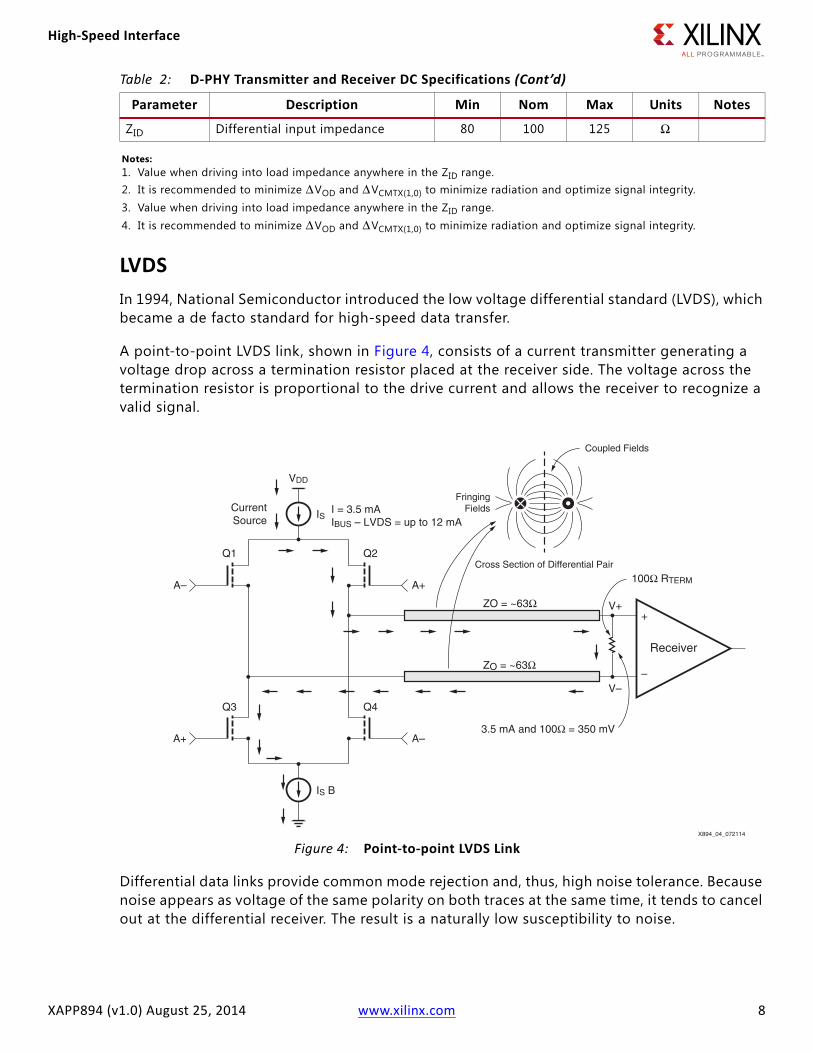
LVDSIn 1994, National Semiconductor introduced the low voltage differential standard (LVDS), which became a de facto standard for high-speed data transfer.
A point-to-point LVDS link, shown in Figure 4, consists of a current transmitter generating a voltage drop across a termination resistor placed at the receiver side. The voltage across the termination resistor is proportional to the drive current and allows the receiver to recognize a valid signal.
Differential data links provide common mode rejection and, thus, high noise tolerance. Because noise appears as voltage of the same polarity on both traces at the same time, it tends to cancel out at the differential receiver. The result is a naturally low susceptibility to noise.
ZID Differential input impedance 80 100 125 Ω
Notes: 1. Value when driving into load impedance anywhere in the ZID range.2. It is recommended to minimize ΔVOD and ΔVCMTX(1,0) to minimize radiation and optimize signal integrity.3. Value when driving into load impedance anywhere in the ZID range.4. It is recommended to minimize ΔVOD and ΔVCMTX(1,0) to minimize radiation and optimize signal integrity.
Table 2: D-PHY Transmitter and Receiver DC Specifications (Cont’d)
Parameter Description Min Nom Max Units Notes
X-Ref Target - Figure 4
Figure 4: Point-to-point LVDS Link
CurrentSource
IS
VDD
3.5 mA and 100Ω = 350 mV
V–
A–
A+
A+
A–
Q2Q1
Q4
IS B
Q3
V++
–
ZO = ~63Ω
ZO = ~63ΩReceiver
Cross Section of Differential Pair
Coupled Fields
FringingFields
100Ω RTERM
X894_04_072114
I = 3.5 mAIBUS – LVDS = up to 12 mA
High-Speed Interface
XAPP894 (v1.0) August 25, 2014 www.xilinx.com 9
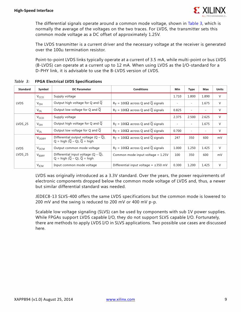
The differential signals operate around a common mode voltage, shown in Table 3, which is normally the average of the voltages on the two traces. For LVDS, the transmitter sets this common mode voltage as a DC offset of approximately 1.25V.
The LVDS transmitter is a current driver and the necessary voltage at the receiver is generated over the 100Ω termination resistor.
Point-to-point LVDS links typically operate at a current of 3.5 mA, while multi-point or bus LVDS (B-LVDS) can operate at a current up to 12 mA. When using LVDS as the I/O-standard for a D-PHY link, it is advisable to use the B-LVDS version of LVDS.
LVDS was originally introduced as a 3.3V standard. Over the years, the power requirements of electronic components dropped below the common mode voltage of LVDS and, thus, a newer but similar differential standard was needed.
JEDEC8-13 SLVS-400 offers the same LVDS specifications but the common mode is lowered to 200 mV and the swing is reduced to 200 mV or 400 mV p-p.
Scalable low voltage signaling (SLVS) can be used by components with sub 1V power supplies. While FPGAs support LVDS capable I/O, they do not support SLVS capable I/O. Fortunately, there are methods to apply LVDS I/O in SLVS applications. Two possible use cases are discussed here.
Table 3: FPGA Electrical LVDS Specifications
Standard Symbol DC Parameter Conditions Min Type Max Units
LVDS
VCCO Supply voltage 1.710 1.800 1.890 V
VOH Output high voltage for Q and Q RT = 100Ω across Q and Q signals - - 1.675 V
VOL Output low voltage for Q and Q RT = 100Ω across Q and Q signals 0.825 - - V
LVDS_25
VCCO Supply voltage 2.375 2.500 2.625 V
VOH Output high voltage for Q and Q RT = 100Ω across Q and Q signals - - 1.675 V
VOL Output low voltage for Q and Q RT = 100Ω across Q and Q signals 0.700 - - V
LVDS
LVDS_25
VODIFF Differential output voltage (Q – Q),Q = high (Q – Q), Q = high
RT = 100Ω across Q and Q signals 247 350 600 mV
VOCM Output common mode voltage RT = 100Ω across Q and Q signals 1.000 1.250 1.425 V
VIDIFF Differential input voltage (Q – Q),Q = high (Q – Q), Q = high
Common mode input voltage = 1.25V 100 350 600 mV
VICM Input common mode voltage Differential input voltage = ±350 mV 0.300 1.200 1.425 V
High-Speed Interface
XAPP894 (v1.0) August 25, 2014 www.xilinx.com 10
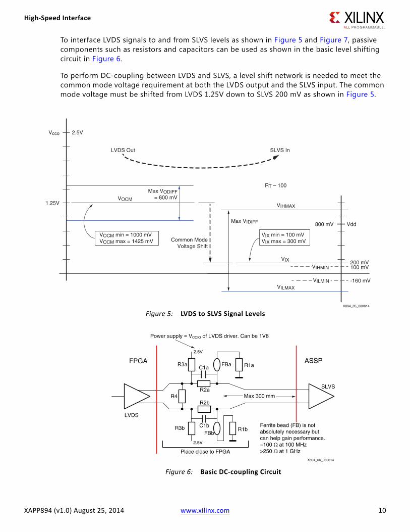
To interface LVDS signals to and from SLVS levels as shown in Figure 5 and Figure 7, passive components such as resistors and capacitors can be used as shown in the basic level shifting circuit in Figure 6.
To perform DC-coupling between LVDS and SLVS, a level shift network is needed to meet the common mode voltage requirement at both the LVDS output and the SLVS input. The common mode voltage must be shifted from LVDS 1.25V down to SLVS 200 mV as shown in Figure 5.
X-Ref Target - Figure 5
Figure 5: LVDS to SLVS Signal Levels
Vcco 2.5V
VOCM1.25V
RT – 100Max VODIFF
= 600 mV
VIX
Vdd800 mV
200 mV
Max VIDIFF
VIHMAX
VILMAX
-160 mV
Common ModeVoltage Shift
LVDS Out SLVS In
VIX min = 100 mVVIX max = 300 mV
VOCM min = 1000 mVVOCM max = 1425 mV
VILMIN
VIHMIN 100 mV
X894_05_080614
X-Ref Target - Figure 6
Figure 6: Basic DC-coupling Circuit
X894_06_080614
LVDS
SLVS
2.5V
R1a
R2a
R3a FBa
Ferrite bead (FB) is not absolutely necessary but can help gain performance.~100 Ω at 100 MHz>250 Ω at 1 GHz
C1a
2.5V
Place close to FPGA
FPGA
R4R2b
C1bFBb
R1bR3b
ASSP
Max 300 mm
Power supply = VCCIO of LVDS driver. Can be 1V8
High-Speed Interface
XAPP894 (v1.0) August 25, 2014 www.xilinx.com 11
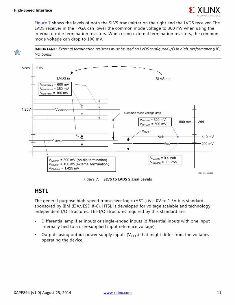
Figure 7 shows the levels of both the SLVS transmitter on the right and the LVDS receiver. The LVDS receiver in the FPGA can lower the common mode voltage to 300 mV when using the internal on-die termination resistors. When using external termination resistors, the common mode voltage can drop to 100 mV.
IMPORTANT: External termination resistors must be used on LVDS configured I/O in high-performance (HP) I/O banks.
HSTLThe general purpose high-speed transceiver logic (HSTL) is a 0V to 1.5V bus standard sponsored by IBM (EIA/JESD 8-6). HTSL is developed for voltage scalable and technology independent I/O structures. The I/O structures required by this standard are:
• Differential amplif ier inputs or single-ended inputs (differential inputs with one input internally tied to a user-supplied input reference voltage).
• Outputs using output power supply inputs (VCCO) that might differ from the voltages operating the device.
X-Ref Target - Figure 7
Figure 7: SLVS to LVDS Signal LevelsX894_09_080614
Vcco 2.5V
VICMAVG1.25V
Vox
Vdd800 mV
200 mV
VohVODIFF
410 mV
Common mode voltage drop
LVDS in SLVS out
VOHMIN = 320 mVVOHMAX = 500 mV
VICMMIN = 300 mV (on-die termination).VICMMIN = 100 mV (external termination)VICMMAX = 1.425 mV
VOXMIN = 0.4 VohVOXMAX = 0.6 Voh
VICMMIN
VIDIFFMAX = 600 mVVIDIFFAVG = 350 mVVIDIFFMIN = 100 mV
High-Speed Interface
XAPP894 (v1.0) August 25, 2014 www.xilinx.com 12
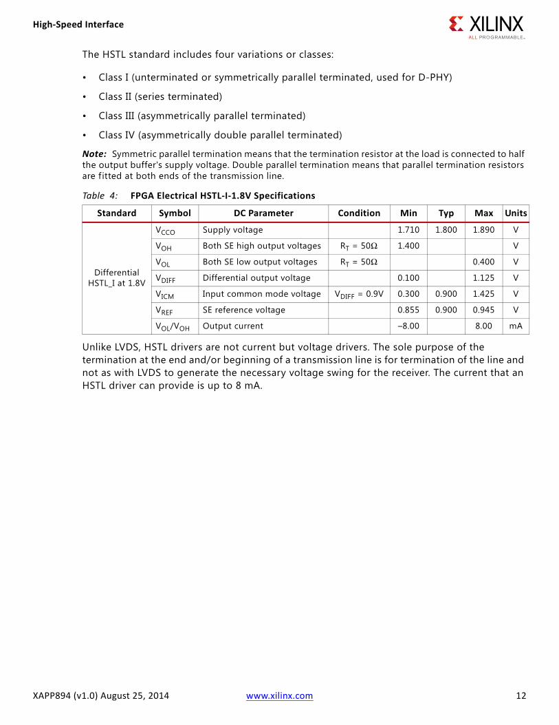
The HSTL standard includes four variations or classes:
• Class I (unterminated or symmetrically parallel terminated, used for D-PHY)
• Class II (series terminated)
• Class III (asymmetrically parallel terminated)
• Class IV (asymmetrically double parallel terminated)
Note: Symmetric parallel termination means that the termination resistor at the load is connected to half the output buffer's supply voltage. Double parallel termination means that parallel termination resistors are f itted at both ends of the transmission line.
Unlike LVDS, HSTL drivers are not current but voltage drivers. The sole purpose of the termination at the end and/or beginning of a transmission line is for termination of the line and not as with LVDS to generate the necessary voltage swing for the receiver. The current that an HSTL driver can provide is up to 8 mA.
Table 4: FPGA Electrical HSTL-I-1.8V Specifications
Standard Symbol DC Parameter Condition Min Typ Max Units
Differential HSTL_I at 1.8V
VCCO Supply voltage 1.710 1.800 1.890 V
VOH Both SE high output voltages RT = 50Ω 1.400 V
VOL Both SE low output voltages RT = 50Ω 0.400 V
VDIFF Differential output voltage 0.100 1.125 V
VICM Input common mode voltage VDIFF = 0.9V 0.300 0.900 1.425 V
VREF SE reference voltage 0.855 0.900 0.945 V
VOL/VOH Output current –8.00 8.00 mA
Low-Power Interface
XAPP894 (v1.0) August 25, 2014 www.xilinx.com 13
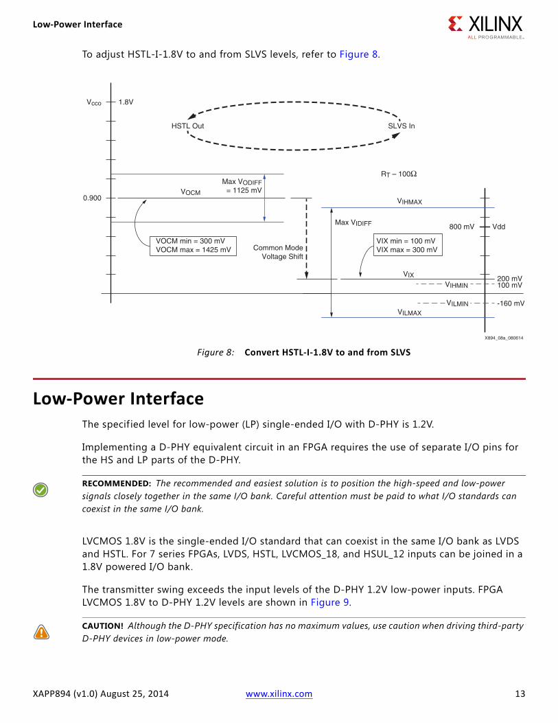
To adjust HSTL-I-1.8V to and from SLVS levels, refer to Figure 8.
Low-Power InterfaceThe specif ied level for low-power (LP) single-ended I/O with D-PHY is 1.2V.
Implementing a D-PHY equivalent circuit in an FPGA requires the use of separate I/O pins for the HS and LP parts of the D-PHY.
RECOMMENDED: The recommended and easiest solution is to position the high-speed and low-power signals closely together in the same I/O bank. Careful attention must be paid to what I/O standards can coexist in the same I/O bank.
LVCMOS 1.8V is the single-ended I/O standard that can coexist in the same I/O bank as LVDS and HSTL. For 7 series FPGAs, LVDS, HSTL, LVCMOS_18, and HSUL_12 inputs can be joined in a 1.8V powered I/O bank.
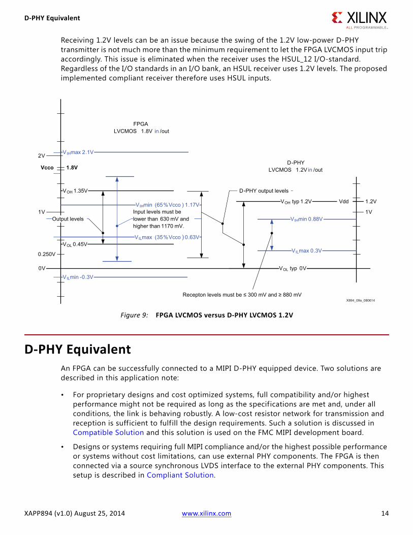
The transmitter swing exceeds the input levels of the D-PHY 1.2V low-power inputs. FPGA LVCMOS 1.8V to D-PHY 1.2V levels are shown in Figure 9.
CAUTION! Although the D-PHY specification has no maximum values, use caution when driving third-party D-PHY devices in low-power mode.
X-Ref Target - Figure 8
Figure 8: Convert HSTL-I-1.8V to and from SLVS
Vcco 1.8V
VOCM0.900
RT – 100ΩMax VODIFF
= 1125 mV
VIX
Vdd800 mV
200 mV
Max VIDIFF
VIHMAX
VILMAX
-160 mV
Common ModeVoltage Shift
HSTL Out SLVS In
VIX min = 100 mVVIX max = 300 mV
VOCM min = 300 mVVOCM max = 1425 mV
VILMIN
VIHMIN 100 mV
X894_08a_080614
D-PHY Equivalent
XAPP894 (v1.0) August 25, 2014 www.xilinx.com 14
Receiving 1.2V levels can be an issue because the swing of the 1.2V low-power D-PHY transmitter is not much more than the minimum requirement to let the FPGA LVCMOS input trip accordingly. This issue is eliminated when the receiver uses the HSUL_12 I/O-standard. Regardless of the I/O standards in an I/O bank, an HSUL receiver uses 1.2V levels. The proposed implemented compliant receiver therefore uses HSUL inputs.
D-PHY EquivalentAn FPGA can be successfully connected to a MIPI D-PHY equipped device. Two solutions are described in this application note:
• For proprietary designs and cost optimized systems, full compatibility and/or highest performance might not be required as long as the specif ications are met and, under all conditions, the link is behaving robustly. A low-cost resistor network for transmission and reception is suff icient to fulf ill the design requirements. Such a solution is discussed in Compatible Solution and this solution is used on the FMC MIPI development board.
• Designs or systems requiring full MIPI compliance and/or the highest possible performance or systems without cost limitations, can use external PHY components. The FPGA is then connected via a source synchronous LVDS interface to the external PHY components. This setup is described in Compliant Solution.
X-Ref Target - Figure 9
Figure 9: FPGA LVCMOS versus D-PHY LVCMOS 1.2V
X894_09a_080614
Vcco 1.8V
FPGALVCMOS 1.8V in /out
VILmin -0.3V
VILmax (35%Vcco ) 0.63V
VIHmin (65%Vcco ) 1.17V
VIHmax 2.1V
VOL 0.45V
VOH 1.35V
Output levelsInput levels must be lower than 630 mV and higher than 1170 mV.
0.250V
0V
2V
1V 1V
1.2V
VOL typ 0V
VOH typ 1.2V Vdd
VILmax 0.3V
VIHmin 0.88V
D-PHY output levels
Recepton levels must be ≤ 300 mV and ≥ 880 mV
D-PHYLVCMOS 1.2V in /out
D-PHY Equivalent
XAPP894 (v1.0) August 25, 2014 www.xilinx.com 15
Compatible SolutionCurrent FPGAs are not equipped with full D-PHY (MIPI) compliant I/O and the provided solution of unidirectional transmitters and receivers is for proprietary use only. The solution is compatible to the D-PHY standard in the way it supports the electrical specifications of the D-PHY and makes it possible for an FPGA to be directly connected to a MIPI compatible component (or a MIPI compatible component can be connected to an FPGA).
Adapting signal levels and connecting different types of I/O with different supply and signal levels can be done in different ways. Speed, cost, and space are the main factors that determine which circuits are used.
The goal is to let the FPGA communicate with a MIPI device at greater than 800 Mb/s over a distance of 300 mm. The circuits of Figure 10 (transmitter) and Figure 11 (receiver) allow communication up to 800 Mb/s between an FPGA and a MIPI device. These setups also allow a loopback connection at the MIPI signal level. The simulation results of the D-PHY compatible transmitter and receiver are shown in the following pages.
The provided examples have been simulated in Hyperlynx and SPICE and are tested in hardware with a D-PHY FMC development board. D-PHY FMC development boards are available for evaluation through your local technical support. The schematic and the simulation setup can be downloaded from https://secure.xilinx.com/webreg/clickthrough.do?cid=363874.
RECOMMENDED: It is recommended to instantiate input buffers (IBUF/IBUFDS) and output (OBUF/OBUFDS) buffers in the design source code. Provide attributes such as IOSTANDARD, DRIVE (use an elevated drive level), and LOCation in the UCF, XDC, and/or source code.
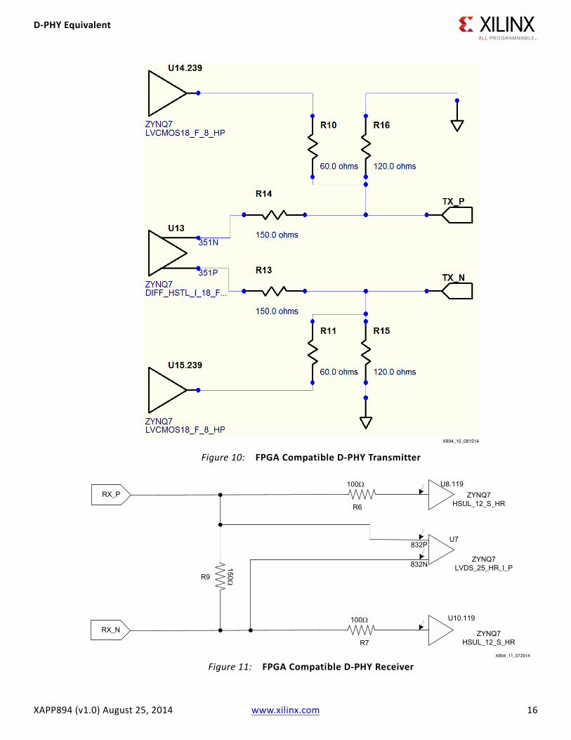
The IOSTANDARD can, depending on the circuit and topology used, be set for differential I/O to LVDS, BLVDS, or HSTL and for single-ended I/O to LVCMOS_1.8V or HSUL_1.2V. On the Xilinx development board, the I/O standards used are shown in Figure 10 and Figure 11.
D-PHY Equivalent
XAPP894 (v1.0) August 25, 2014 www.xilinx.com 16
X-Ref Target - Figure 10
Figure 10: FPGA Compatible D-PHY TransmitterX-Ref Target - Figure 11
Figure 11: FPGA Compatible D-PHY Receiver
D-PHY Equivalent
XAPP894 (v1.0) August 25, 2014 www.xilinx.com 17
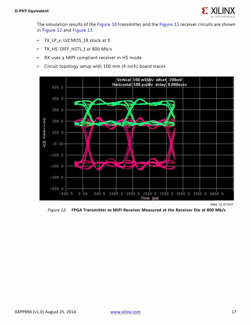
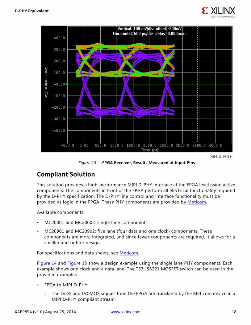
The simulation results of the Figure 10 transmitter and the Figure 11 receiver circuits are shown in Figure 12 and Figure 13.
• TX_LP_x: LVCMOS_18 stuck at 0
• TX_HS: DIFF_HSTL_I at 800 Mb/s
• RX uses a MIPI compliant receiver in HS mode
• Circuit topology setup with 100 mm (4-inch) board tracesX-Ref Target - Figure 12
Figure 12: FPGA Transmitter to MIPI Receiver Measured at the Receiver Die at 800 Mb/s
D-PHY Equivalent
XAPP894 (v1.0) August 25, 2014 www.xilinx.com 18
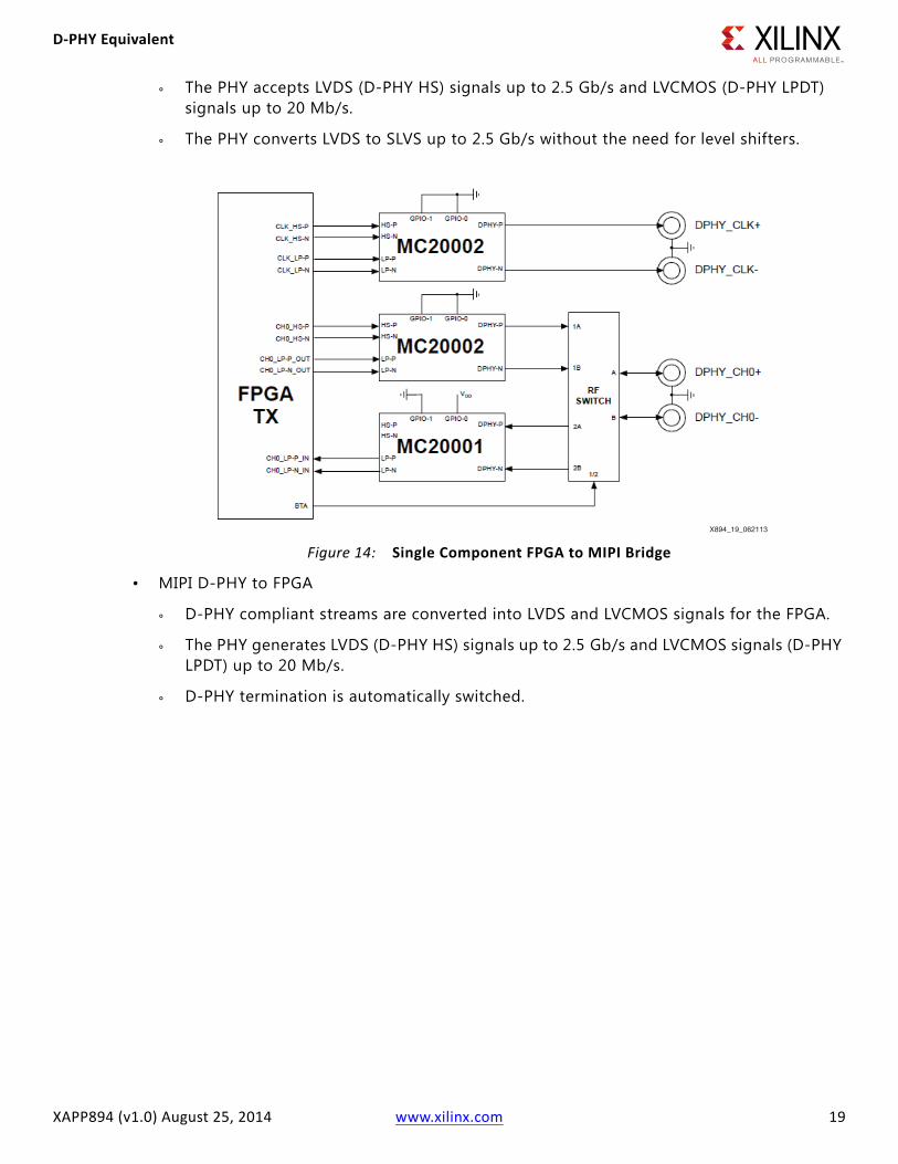
Compliant SolutionThis solution provides a high-performance MIPI D-PHY interface at the FPGA level using active components. The components in front of the FPGA perform all electrical functionality required by the D-PHY specification. The D-PHY line control and interface functionality must be provided as logic in the FPGA. These PHY components are provided by Meticom.
Available components:
• MC20001 and MC20002: single lane components.
• MC20901 and MC20902: f ive lane (four data and one clock) components. These components are more integrated, and since fewer components are required, it allows for a smaller and tighter design.
For specif ications and data sheets, see Meticom.
Figure 14 and Figure 15 show a design example using the single lane PHY components. Each example shows one clock and a data lane. The TS3USB221 MOSFET switch can be used in the provided examples.
• FPGA to MIPI D-PHY
° The LVDS and LVCMOS signals from the FPGA are translated by the Meticom device in a MIPI D-PHY compliant stream.
X-Ref Target - Figure 13
Figure 13: FPGA Receiver, Results Measured at Input Pins
D-PHY Equivalent
XAPP894 (v1.0) August 25, 2014 www.xilinx.com 19
° The PHY accepts LVDS (D-PHY HS) signals up to 2.5 Gb/s and LVCMOS (D-PHY LPDT) signals up to 20 Mb/s.
° The PHY converts LVDS to SLVS up to 2.5 Gb/s without the need for level shifters.
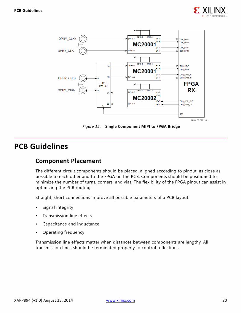
• MIPI D-PHY to FPGA
° D-PHY compliant streams are converted into LVDS and LVCMOS signals for the FPGA.
° The PHY generates LVDS (D-PHY HS) signals up to 2.5 Gb/s and LVCMOS signals (D-PHY LPDT) up to 20 Mb/s.
° D-PHY termination is automatically switched.
X-Ref Target - Figure 14
Figure 14: Single Component FPGA to MIPI BridgeX894_19_062113
PCB Guidelines
XAPP894 (v1.0) August 25, 2014 www.xilinx.com 20
PCB Guidelines
Component PlacementThe different circuit components should be placed, aligned according to pinout, as close as possible to each other and to the FPGA on the PCB. Components should be positioned to minimize the number of turns, corners, and vias. The flexibility of the FPGA pinout can assist in optimizing the PCB routing.
Straight, short connections improve all possible parameters of a PCB layout:
• Signal integrity
• Transmission line effects
• Capacitance and inductance
• Operating frequency
Transmission line effects matter when distances between components are lengthy. All transmission lines should be terminated properly to control reflections.
X-Ref Target - Figure 15
Figure 15: Single Component MIPI to FPGA BridgeX894_20_062113

PCB Guidelines
XAPP894 (v1.0) August 25, 2014 www.xilinx.com 21
Guidelines and RecommendationsThe key guidelines for PCB designers are:
• Spend suff icient time when placing components for the layout.
• Keep trace lengths as short as possible.
• Place the necessary resistors and capacitors as close as possible to the FPGA.
• Spend time determining the number of PCB layers and how the layer stack-up is realized.
• If possible, during PCB layout, keep the length of a track shorter than the travel and reflection time of the signal on the trace. If this is not possible, take transmission line theory into account.
• Match the length of all differential traces (data and clock).
• When making turns with differential traces, balance the number of left and right turns.
• When making a turn with a differential trace, the inner trace becomes shorter than the outer trace of the pair. When using more turns in one direction, one trace of the differential pair is longer than the other (without direct correction possibilities).
• Do not route traces into 90° or 180° turns. Such turns increase the effective width of the trace, contributing to parasitic capacitance. At very fast edge rates, these discontinuities can cause significant signal integrity problems. Instead, use round, circular turns. If this is not possible, use 45° corners.
• Spread traces after routing over the available space of the PCB to minimize crosstalk.
• Take the guidelines of the signal return paths into account!
• Guard traces when necessary.
• Remember the importance of ground planes.
• Use dedicated and separate planes for power and ground.
• Run high-speed signals on the outer layers of the PCB. Signals run faster on outer PCB layers.
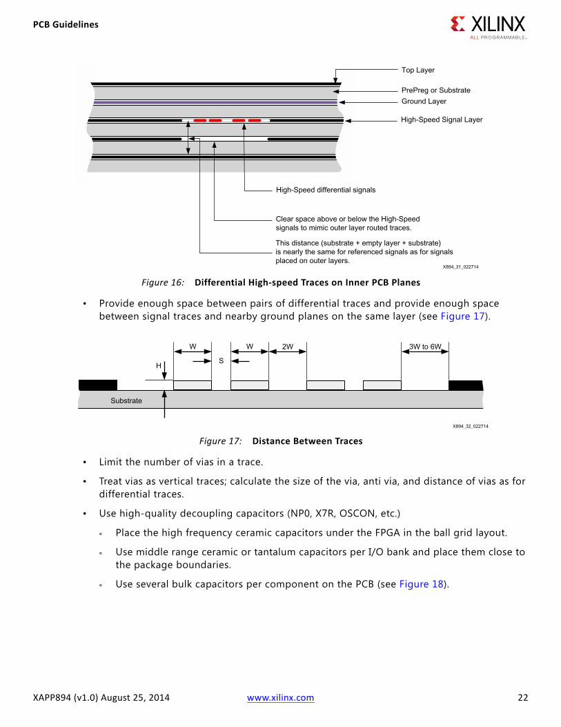
• If high-speed signals are laid out on inner PCB layers, provide room to mimic traces on the outer layers (see Figure 16).
PCB Guidelines
XAPP894 (v1.0) August 25, 2014 www.xilinx.com 22
• Provide enough space between pairs of differential traces and provide enough space between signal traces and nearby ground planes on the same layer (see Figure 17).
• Limit the number of vias in a trace.
• Treat vias as vertical traces; calculate the size of the via, anti via, and distance of vias as for differential traces.
• Use high-quality decoupling capacitors (NP0, X7R, OSCON, etc.)
° Place the high frequency ceramic capacitors under the FPGA in the ball grid layout.
° Use middle range ceramic or tantalum capacitors per I/O bank and place them close to the package boundaries.
° Use several bulk capacitors per component on the PCB (see Figure 18).
X-Ref Target - Figure 16
Figure 16: Differential High-speed Traces on Inner PCB Planes
X-Ref Target - Figure 17
Figure 17: Distance Between Traces
Conclusion
XAPP894 (v1.0) August 25, 2014 www.xilinx.com 23
ConclusionThe use of external circuits, such as those presented in this application, make it possible to connect an FPGA to an ASSP device via its MIPI interface. Compatible or proprietary solutions use FPGA I/O configured as BLVDS or DIFF_HSTL_I_18 for HS traffic and LVCMOS_18 and/or HSUL_12 for LP traff ic while compliant solutions use FPGA I/O configured as LVDS for connection to external supplied PHY components.
Revision HistoryThe following table shows the revision history for this document.
Please Read: Important Legal NoticesThe information disclosed to you hereunder (the “Materials”) is provided solely for the selection and use of Xilinx products. To the maximum extent permitted by applicable law: (1) Materials are made available "AS IS" and with all faults, Xilinx hereby DISCLAIMS ALL WARRANTIES AND CONDITIONS, EXPRESS, IMPLIED, OR STATUTORY, INCLUDING BUT NOT LIMITED TO WARRANTIES OF MERCHANTABILITY, NON-INFRINGEMENT, OR FITNESS FOR ANY PARTICULAR PURPOSE; and (2) Xilinx shall not be liable (whether in contract or tort, including negligence, or under any other theory of liability) for any loss or damage of any kind or nature related to, arising under, or in connection with, the Materials (including your use of the Materials), including for any direct, indirect, special, incidental, or consequential loss or damage (including loss of data, profits, goodwill, or any type of loss or damage suffered as a result of any action brought by a third party) even if such damage or loss was reasonably foreseeable or Xilinx had been advised of the possibility of the same. Xilinx assumes no obligation to correct any errors contained in the Materials or to notify you of updates to the Materials or to product specifications. You may not reproduce, modify, distribute, or publicly display the Materials without prior written consent. Certain products are subject to the terms and conditions of Xilinx’s limited warranty, please refer to Xilinx’s Terms of Sale which can be viewed at http://www.xilinx.com/legal.htm#tos; IP cores may be subject to warranty and support terms contained in a license
X-Ref Target - Figure 18
Figure 18: PCB and the Decoupling Capacitor Coverage
Date Version Revision
08/25/2014 1.0 Initial Xilinx release.
Please Read: Important Legal Notices
XAPP894 (v1.0) August 25, 2014 www.xilinx.com 24
issued to you by Xilinx. Xilinx products are not designed or intended to be fail-safe or for use in any application requiring fail-safe performance; you assume sole risk and liability for use of Xilinx products in such critical applications, please refer to Xilinx’s Terms of Sale which can be viewed at http://www.xilinx.com/legal.htm#tos.Automotive Applications DisclaimerXILINX PRODUCTS ARE NOT DESIGNED OR INTENDED TO BE FAIL-SAFE, OR FOR USE IN ANY APPLICATION REQUIRING FAIL-SAFE PERFORMANCE, SUCH AS APPLICATIONS RELATED TO: (I) THE DEPLOYMENT OF AIRBAGS, (II) CONTROL OF A VEHICLE, UNLESS THERE IS A FAIL-SAFE OR REDUNDANCY FEATURE (WHICH DOES NOT INCLUDE USE OF SOFTWARE IN THE XILINX DEVICE TO IMPLEMENT THE REDUNDANCY) AND A WARNING SIGNAL UPON FAILURE TO THE OPERATOR, OR (III) USES THAT COULD LEAD TO DEATH OR PERSONAL INJURY. CUSTOMER ASSUMES THE SOLE RISK AND LIABILITY OF ANY USE OF XILINX PRODUCTS IN SUCH APPLICATIONS.© Copyright 2014 Xilinx, Inc. Xilinx, the Xilinx logo, Artix, ISE, Kintex, Spartan, Virtex, Vivado, Zynq, and other designated brands included herein are trademarks of Xilinx in the United States and other countries. All other trademarks are the property of their respective owners.
Related Documents


