Cypress Semiconductor 198 Champion Court San Jose, CA 95134-1709 www.cypress.com CYUSB43xx EZ-USB HX3PD Programming Specification Document Number: 002-27814 Rev. **

Welcome message from author
This document is posted to help you gain knowledge. Please leave a comment to let me know what you think about it! Share it to your friends and learn new things together.
Transcript
Cypress Semiconductor198 Champion Court
San Jose, CA 95134-1709www.cypress.com
CYUSB43xx
EZ-USB HX3PD Programming SpecificationDocument Number: 002-27814 Rev. **
Copyrights
CYUSB43xx EZ-USB HX3PD Programming Specification, Document Number: 002-27814 Rev. ** 2
Copyrights
© Cypress Semiconductor Corporation, 2019. This document is the property of Cypress Semiconductor Corporation and itssubsidiaries ("Cypress"). This document, including any software or firmware included or referenced in this document ("Soft-ware"), is owned by Cypress under the intellectual property laws and treaties of the United States and other countries world-wide. Cypress reserves all rights under such laws and treaties and does not, except as specifically stated in this paragraph,grant any license under its patents, copyrights, trademarks, or other intellectual property rights. If the Software is not accom-panied by a license agreement and you do not otherwise have a written agreement with Cypress governing the use of theSoftware, then Cypress hereby grants you a personal, non-exclusive, nontransferable license (without the right to sublicense)(1) under its copyright rights in the Software (a) for Software provided in source code form, to modify and reproduce the Soft-ware solely for use with Cypress hardware products, only internally within your organization, and (b) to distribute the Softwarein binary code form externally to end users (either directly or indirectly through resellers and distributors), solely for use onCypress hardware product units, and (2) under those claims of Cypress's patents that are infringed by the Software (as pro-vided by Cypress, unmodified) to make, use, distribute, and import the Software solely for use with Cypress hardware prod-ucts. Any other use, reproduction, modification, translation, or compilation of the Software is prohibited.
TO THE EXTENT PERMITTED BY APPLICABLE LAW, CYPRESS MAKES NO WARRANTY OF ANY KIND, EXPRESS ORIMPLIED, WITH REGARD TO THIS DOCUMENT OR ANY SOFTWARE OR ACCOMPANYING HARDWARE, INCLUDING,BUT NOT LIMITED TO, THE IMPLIED WARRANTIES OF MERCHANTABILITY AND FITNESS FOR A PARTICULAR PUR-POSE. No computing device can be absolutely secure. Therefore, despite security measures implemented in Cypress hard-ware or software products, Cypress shall have no liability arising out of any security breach, such as unauthorized access toor use of a Cypress product. CYPRESS DOES NOT REPRESENT, WARRANT, OR GUARANTEE THAT CYPRESS PROD-UCTS, OR SYSTEMS CREATED USING CYPRESS PRODUCTS, WILL BE FREE FROM CORRUPTION, ATTACK,VIRUSES, INTERFERENCE, HACKING, DATA LOSS OR THEFT, OR OTHER SECURITY INTRUSION (collectively, "Secu-rity Breach"). Cypress disclaims any liability relating to any Security Breach, and you shall and hereby do release Cypressfrom any claim, damage, or other liability arising from any Security Breach. In addition, the products described in these mate-rials may contain design defects or errors known as errata which may cause the product to deviate from published specifica-tions. To the extent permitted by applicable law, Cypress reserves the right to make changes to this document without furthernotice. Cypress does not assume any liability arising out of the application or use of any product or circuit described in thisdocument. Any information provided in this document, including any sample design information or programming code, is pro-vided only for reference purposes. It is the responsibility of the user of this document to properly design, program, and testthe functionality and safety of any application made of this information and any resulting product. "High-Risk Device" meansany device or system whose failure could cause personal injury, death, or property damage. Examples of High-Risk Devicesare weapons, nuclear installations, surgical implants, and other medical devices. "Critical Component" means any compo-nent of a High-Risk Device whose failure to perform can be reasonably expected to cause, directly or indirectly, the failure ofthe High-Risk Device, or to affect its safety or effectiveness. Cypress is not liable, in whole or in part, and you shall andhereby do release Cypress from any claim, damage, or other liability arising from any use of a Cypress product as a CriticalComponent in a High-Risk Device. You shall indemnify and hold Cypress, its directors, officers, employees, agents, affiliates,distributors, and assigns harmless from and against all claims, costs, damages, and expenses, arising out of any claim,including claims for product liability, personal injury or death, or property damage arising from any use of a Cypress productas a Critical Component in a High-Risk Device. Cypress products are not intended or authorized for use as a Critical Compo-nent in any High-Risk Device except to the limited extent that (i) Cypress's published data sheet for the product explicitlystates Cypress has qualified the product for use in a specific High-Risk Device, or (ii) Cypress has given you advance writtenauthorization to use the product as a Critical Component in the specific High-Risk Device and you have signed a separateindemnification agreement.
Cypress, the Cypress logo, Spansion, the Spansion logo, and combinations thereof, WICED, PSoC, CapSense, EZ-USB, F-RAM, and Traveo are trademarks or registered trademarks of Cypress in the United States and other countries. For a morecomplete list of Cypress trademarks, visit cypress.com. Other names and brands may be claimed as property of their respec-tive owners.
CYUSB43xx EZ-USB HX3PD Programming Specification, Document Number: 002-27814 Rev. ** 3
Contents
1. Introduction 4
1.1 Target Devices ...................................................................................................................................................... 4
1.2 Programmer........................................................................................................................................................... 4
1.3 Target Overview .................................................................................................................................................... 5
2. Required Data 6
2.1 Hex File Origin....................................................................................................................................................... 6
2.2 Nonvolatile Subsystem.......................................................................................................................................... 6
2.3 Organization of the Hex File .................................................................................................................................. 8
3. Communication Interface 10
3.1 The Protocol Stack .............................................................................................................................................. 10
3.2 SWD Interface ..................................................................................................................................................... 11
3.3 Hardware Access Commands............................................................................................................................. 12
3.4 Pseudocode......................................................................................................................................................... 13
3.5 Physical Layer ..................................................................................................................................................... 14
4. Programming Algorithm 16
4.1 High-Level Programming Flow ............................................................................................................................ 16
4.2 Subroutines Used in the Programming Flow....................................................................................................... 17
4.3 Step 1A – Acquire the Chip After Hard Reset ..................................................................................................... 19
4.4 Step 1B – Acquire Chip (Alternate Method) ........................................................................................................ 22
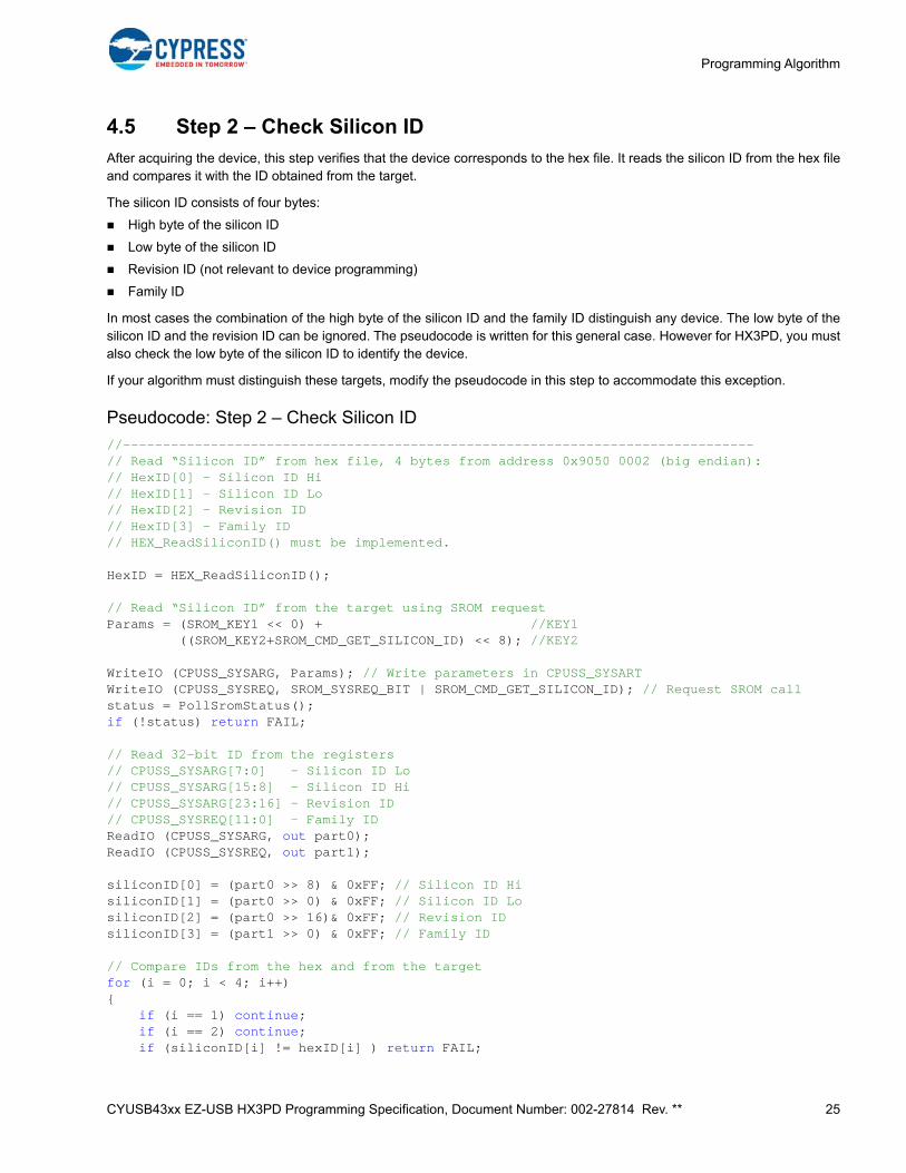
4.5 Step 2 – Check Silicon ID.................................................................................................................................... 25
4.6 Step 3 – Erase All Flash...................................................................................................................................... 26
4.7 Step 4 – Checksum Privileged ............................................................................................................................ 27
4.8 Step 5 – Program Flash....................................................................................................................................... 27
4.9 Step 6 – Verify Flash ........................................................................................................................................... 31
4.10 Step 7 – Program Protection Settings ................................................................................................................. 32
4.11 Step 8 – Verify Protection Settings...................................................................................................................... 35
4.12 Step 9 – Verify Checksum................................................................................................................................... 38
4.13 Step 10 – Program User SFlash (optional).......................................................................................................... 39
A Chip-Level Protection 43
B Intel Hex File Format 45
C Serial Wire Debug (SWD) Protocol 46
D Timing Specifications of the SWD Interface 48
Revision History 49
CYUSB43xx EZ-USB HX3PD Programming Specification, Document Number: 002-27814 Rev. ** 4
1. Introduction
This document provides a generic description of the programming specification necessary to program nonvolatile memory forthe target devices. The document uses the word “target” as the generic name for all devices supported by this manual. Itdescribes the communication protocol required for access by an external programmer, and explains the programming algo-rithm. The programming algorithms described in the following sections are compatible with all target devices. There are differ-ences among the various devices, for example in row size. This document details any differences.
This programming specification is intended for those developing programming solutions for the target devices. This includesthird-party production programmers, as well as customers wanting to develop their own programming systems. Informationon Cypress programming solutions is available here: http://www.cypress.com/products/psoc-programming-solutions.
1.1 Target Devices
This manual covers the following devices:
CYUSB43xx
1.2 Programmer
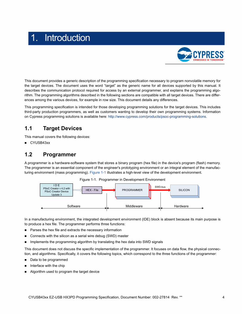
A programmer is a hardware-software system that stores a binary program (hex file) in the device's program (flash) memory.The programmer is an essential component of the engineer's prototyping environment or an integral element of the manufac-turing environment (mass programming). Figure 1-1 illustrates a high-level view of the development environment.
Figure 1-1. Programmer in Development Environment
In a manufacturing environment, the integrated development environment (IDE) block is absent because its main purpose isto produce a hex file. The programmer performs three functions:
Parses the hex file and extracts the necessary information
Connects with the silicon as a serial wire debug (SWD) master
Implements the programming algorithm by translating the hex data into SWD signals
This document does not discuss the specific implementation of the programmer. It focuses on data flow, the physical connec-tion, and algorithms. Specifically, it covers the following topics, which correspond to the three functions of the programmer:
Data to be programmed
Interface with the chip
Algorithm used to program the target device
PROGRAMMER SILICON
I D EPSoC Creator v 4.2 with
PSoC Creator Device Update 3
HEX - File
Software HardwareMiddleware
SWD-bus
CYUSB43xx EZ-USB HX3PD Programming Specification, Document Number: 002-27814 Rev. ** 5
Introduction
1.3 Target Overview
EZ-USB® HX3PD is a family of USB 3.1 Gen 2 Type-C hubs with USB Power Delivery (PD) that complies with the USB 3.1Gen 2 (10 Gbps) specification, and the latest Type-C and PD standards. HX3PD consists of a hub controller supporting USB3.1 Gen 2 and USB 2.0 standards, a USB PD controller, and a Dock Management Controller (DMC). The USB PD controllerand DMC can be programmed independently using the details available in this document. HX3PD provides unique SWDinterfaces for the USB PD controller and the DMC. Refer to the HX3PD datasheet for more details.
Note that the firmware for the hub controller needs to be stored in an external EEPROM, which is interfaced with HX3PD overSPI. Refer to the HX3PD datasheet and AN222944 - HX3PD Hardware Design Guidelines and Checklist for details on inter-facing an EEPROM with HX3PD. For programming the external EEPROM with the hub controller firmware, see the respectiveEEPROM programming guide. Programming all the controllers (Hub controller, USB PD controller, and DMC) is mandatory tomake the HX3PD operational.
The word "target" in rest of the document stands for HX3PD's USB PD controller or DMC based on the controller which needsto be programmed. These controllers can be programmed independently in any order.
Table 1-1 summarizes the devices covered by this document. It details the principal programming-related features, and thevalues are for each device series. This document refers to this table when the programming details vary among the targetdevices. The part can be programmed after it is installed in the system by using the SWD interface.
This document focuses on the specific programming operations without referencing the silicon architecture. You are referredto the table above. See the appendices for additional details. This document includes four appendices:
Appendix A. Chip-Level Protection on page 43
Appendix B. Intel Hex File Format on page 45
Appendix C. Serial Wire Debug (SWD) Protocol on page 46
Appendix D. Timing Specifications of the SWD Interface on page 48
Other device-specific information such as electrical characteristics, can be found in the target’s datasheet and in the TechnicalReference Manual.
Table 1-1. Programming Values
FeatureCYUSB43xx
USB PD Controller DMC
CPU CM0
SWD ID 0x0BB1 1477
Silicon IDa
a. See “Step 2 – Check Silicon ID” on page 25 for information on the Silicon ID
0x1F8xxxAF 0x1D8xxxAD
Row Size (bytes) 256 128
Number of Macros 1 2
Rows Per Macro 512
SWT_IMO_48MHZ Required for Flash Operationsb
b. See the pseudocode for “Step 1A – Acquire the Chip After Hard Reset” on page 19 or “Step 1B – Acquire Chip (Alternate Method)” on page 22
Yes
Flash Protection Address Increment for Each Arrayc
c. Required for “Step 8 – Verify Protection Settings” on page 35 in devices with multiple flash arrays
n/a 0x400
CYUSS_SYSREQ Register Address 0x4010 0004
CPUSS_SYSARG Register Address 0x4010 0008
SRAM_PARAMS_BASEd
d. SRAM starting address for storing SROM parameters like flash row data
0x2000 0100
TEST_MODE Register Address 0x4003 0014
SFLASH_MACRO_0 Address 0x0FFF F000
SFLASH_MACRO_1 Address n/a 0x0FFF F400
CYUSB43xx EZ-USB HX3PD Programming Specification, Document Number: 002-27814 Rev. ** 6
2. Required Data
This chapter describes the information that the programmer must extract from the hex file to program the target silicon.
2.1 Hex File Origin
Customers use PSoC Creator or a third-party IDE to develop their projects. After development is completed, the nonvolatileconfiguration of the silicon is saved in the file. Only three records in this file actually refer to flash memory:
User’s program (code)
Flash row-level protection
Chip-level protection
Other records are auxiliary and are used to maintain the integrity of the programming flow.
2.2 Nonvolatile Subsystem
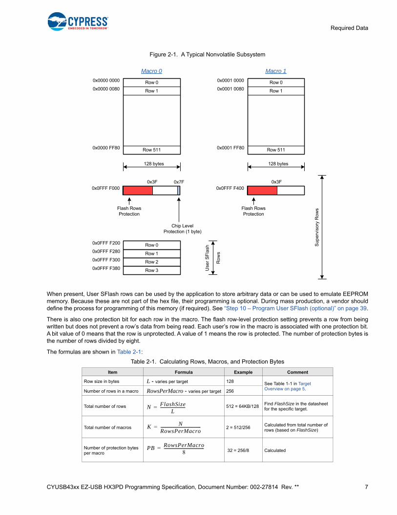
The size of flash memory varies depending on the target. Flash organization varies per target as well. A device may have oneor two macros. The size of a row (the number of bytes per flash row) and the number of rows per flash macro also varies. SeeTable 1-1 in Target Overview on page 5 for details some of these differences.
A programmer writes one row at a time. The number of rows varies based on the size of the flash memory. In addition to theusers' rows, the flash macros contain supervisory rows, which store:
Row-level protection bits
Chip-level protection byte (only in macro 0)
Application-specific information (up to four rows, and only in macro 0 when present) - User Supervisory Flash (SFlash)
User flash programming must take into account the number of rows, bytes per row, the number of macros, and other vari-ables. Figure 2-1 shows a typical flash organization, with 512 rows of 128 bytes, and two macros. Your device may have onlyone macro, with a different number of rows and bytes/row. Other critical values may vary as well. For example, for somedevices the offset for the chip level protection byte in the Supervisory row is 0x7F, as in the figure. In others, the offset is 0xFF.
Refer to Table 1-1 in “Target Overview” on page 5 to determine the actual flash organization for your target. See the targetdatasheet for the flash size. Determine the number of macros by dividing the number of rows by the number of rows permacro.
CYUSB43xx EZ-USB HX3PD Programming Specification, Document Number: 002-27814 Rev. ** 7
Required Data
Figure 2-1. A Typical Nonvolatile Subsystem
When present, User SFlash rows can be used by the application to store arbitrary data or can be used to emulate EEPROMmemory. Because these are not part of the hex file, their programming is optional. During mass production, a vendor shoulddefine the process for programming of this memory (if required). See “Step 10 – Program User SFlash (optional)” on page 39.
There is also one protection bit for each row in the macro. The flash row-level protection setting prevents a row from beingwritten but does not prevent a row’s data from being read. Each user’s row in the macro is associated with one protection bit.A bit value of 0 means that the row is unprotected. A value of 1 means the row is protected. The number of protection bytes isthe number of rows divided by eight.
The formulas are shown in Table 2-1:
Table 2-1. Calculating Rows, Macros, and Protection Bytes
Item Formula Example Comment
Row size in bytes L - varies per target 128 See Table 1-1 in Target Overview on page 5.Number of rows in a macro RowsPerMacro - varies per target 256
Total number of rows 512 = 64KB/128Find FlashSize in the datasheet for the specific target.
Total number of macros 2 = 512/256Calculated from total number of rows (based on FlashSize)
Number of protection bytes per macro
32 = 256/8 Calculated
Row 0
Row 1
Row 511
128 bytes
Macro 0
0x0000 0000
0x0000 0080
0x0000 FF80
0x0FFF F000
Flash RowsProtection
Chip LevelProtection (1 byte)
0x7F0x3F
Row 0
Row 1
Row 511
128 bytes
Macro 1
0x0001 0000
0x0001 0080
0x0001 FF80
0x0FFF F400
Flash RowsProtection
Su
pe
rvis
ory
Ro
ws
0x3F
0x0FFF F200 Row 00x0FFF F280 Row 10x0FFF F300 Row 20x0FFF F380 Row 3 U
ser
SF
lash
Ro
ws
N FlashSizeL
--------------------------=
K NRowsPerMacro-----------------------------------------=
PB RowsPerMacro8
-----------------------------------------=
CYUSB43xx EZ-USB HX3PD Programming Specification, Document Number: 002-27814 Rev. ** 8
Required Data
Flash memory is mapped directly to the CPU’s address space starting at 0x00000000. Therefore, the firmware or externalprogrammer can read its content directly from the given address.
The last type of nonvolatile information in flash is chip-level protection. This consists of one byte that restricts access to thechip’s resources (register, SRAM, and flash) by an external programmer or debugger. For example, in PROTECTED mode,the programmer cannot read or write either flash or SRAM; in KILL mode, the SWD interface is locked in silicon and the chipcannot be reprogrammed. The chip-level protection setting is programmed along with the flash row-level protection into thesupervisory row of the macro (see Figure 2-1), along with the flash row-level protection. For more information about chip-levelprotection, see Appendix A: Chip-Level Protection on page 43.
2.3 Organization of the Hex File
The hex file describes the nonvolatile configuration of the project. It is the data source for the programmer.
The hex file follows the Intel Hex File format. Intel's specification is generic and defines only some types of records in the hexfile. The specification allows customizing the format for any possible silicon architecture. The silicon vendor defines the func-tional meaning of the records, which typically varies for different chip families. See Appendix B: Intel Hex File Format onpage 45 for details of the Intel Hex File format.
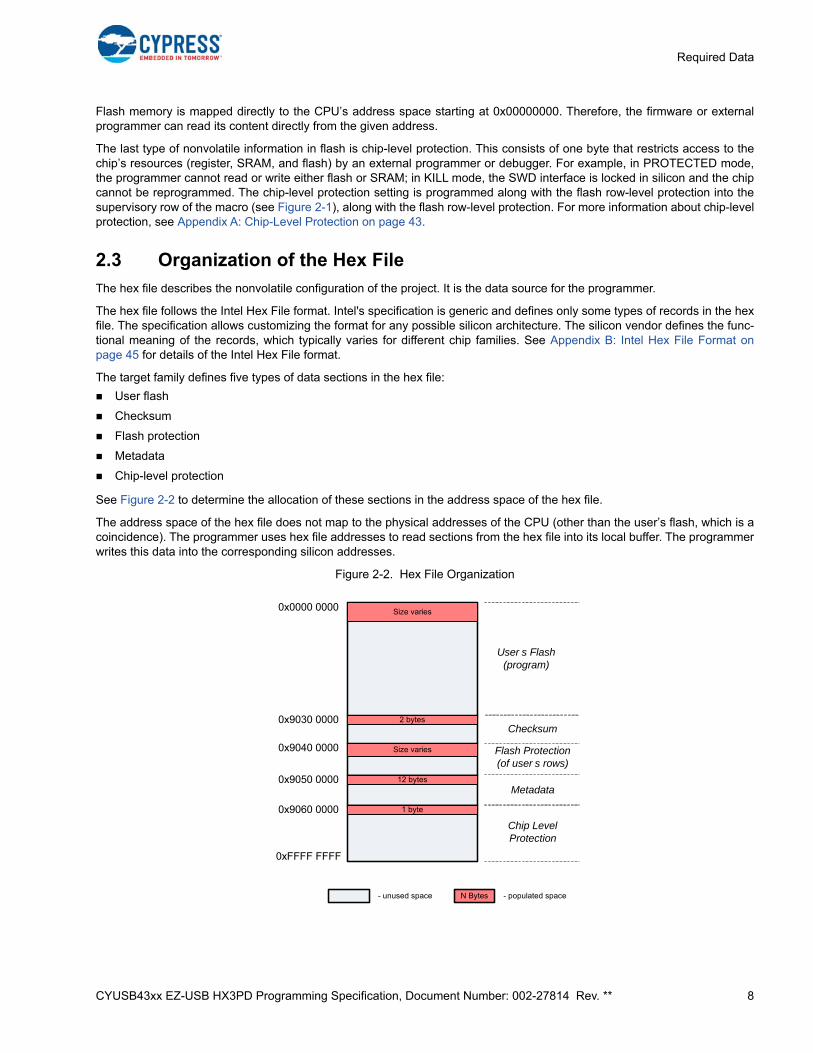
The target family defines five types of data sections in the hex file:
User flash
Checksum
Flash protection
Metadata
Chip-level protection
See Figure 2-2 to determine the allocation of these sections in the address space of the hex file.
The address space of the hex file does not map to the physical addresses of the CPU (other than the user’s flash, which is acoincidence). The programmer uses hex file addresses to read sections from the hex file into its local buffer. The programmerwrites this data into the corresponding silicon addresses.
Figure 2-2. Hex File Organization
0x0000 0000 Size varies
0x9030 0000 2 bytes
0x9040 0000 Size varies
0x9050 0000 12 bytes
0x9060 0000 1 byte
0xFFFF FFFF
User s Flash(program)
Checksum
Flash Protection (of user s rows)
Metadata
Chip Level Protection
N Bytes- unused space - populated space
CYUSB43xx EZ-USB HX3PD Programming Specification, Document Number: 002-27814 Rev. ** 9
Required Data
0x0000 0000 – User’s Flash (size varies): This is the user’s program (code) that must be programmed. The size of this sec-tion matches the flash size of the target part. The programmer can either read all of this section at once or gradually by blockswhere each block is equal to the row size for the device. The programming of the flash is carried out on the basis of one rowfor each request. See table 1-1 in “Target Overview” on page 5 for the row size for each device series.
0x9030 0000 – Checksum (2 bytes): This is the checksum of the entire user flash section—the arithmetical sum of everybyte in the user’s flash. Only two least significant bytes (LSB) of the result are saved in this section, in big-endian format(most significant byte (MSB) first). This must be used by the programmer to check the integrity of the hex file and to verify thequality of the programming. In this context, “integrity” means that the checksum and user’s flash sections must be correlatedin this file. At the end of programming, the checksum of flash (two LSBs) is compared to the checksum from the hex file.
0x9040 0000 – Flash Protection (number of bytes varies): This data is programmed into supervisory rows of the flash mac-ros (see Figure 2-1 on page 7). Every bit defines the write-protection setting for the corresponding user row. The number ofbytes to be read from this section depends on the flash size.
Protection Size = Flash Size / Row Size / 8
Therefore, for a 128 KB part, flash protection consists of 128 bytes.
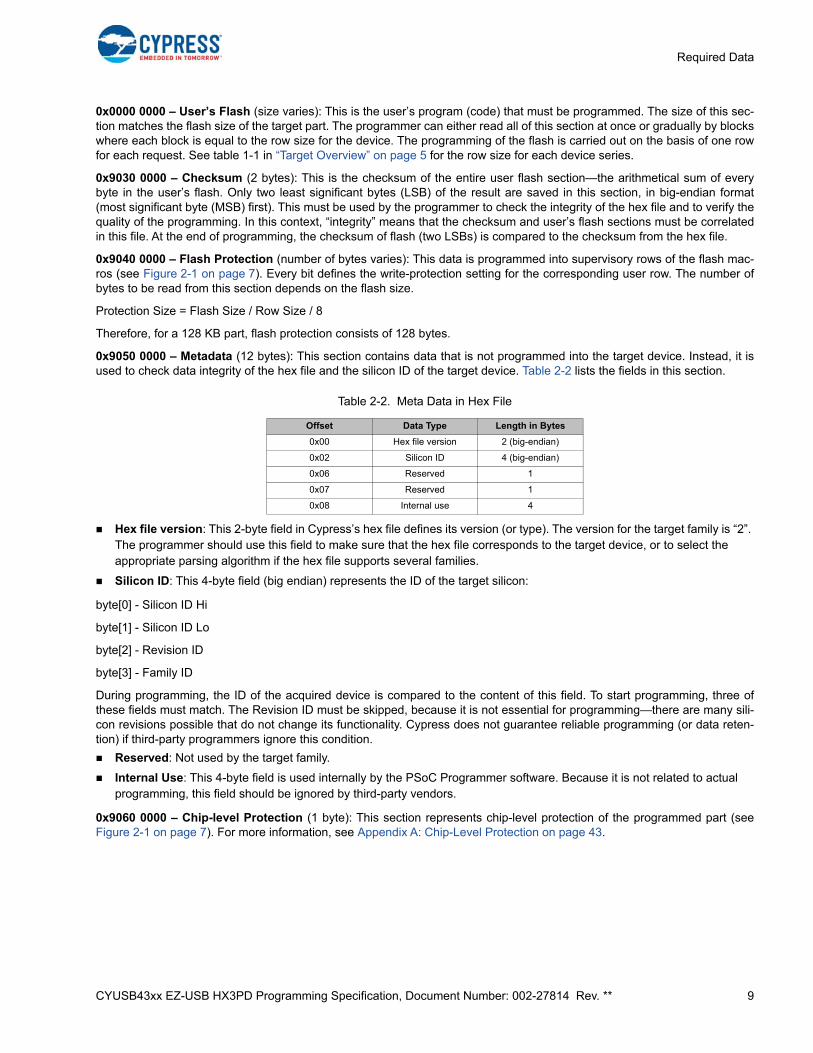
0x9050 0000 – Metadata (12 bytes): This section contains data that is not programmed into the target device. Instead, it isused to check data integrity of the hex file and the silicon ID of the target device. Table 2-2 lists the fields in this section.
Table 2-2. Meta Data in Hex File
Hex file version: This 2-byte field in Cypress’s hex file defines its version (or type). The version for the target family is “2”. The programmer should use this field to make sure that the hex file corresponds to the target device, or to select the appropriate parsing algorithm if the hex file supports several families.
Silicon ID: This 4-byte field (big endian) represents the ID of the target silicon:
byte[0] - Silicon ID Hi
byte[1] - Silicon ID Lo
byte[2] - Revision ID
byte[3] - Family ID
During programming, the ID of the acquired device is compared to the content of this field. To start programming, three ofthese fields must match. The Revision ID must be skipped, because it is not essential for programming—there are many sili-con revisions possible that do not change its functionality. Cypress does not guarantee reliable programming (or data reten-tion) if third-party programmers ignore this condition.
Reserved: Not used by the target family.
Internal Use: This 4-byte field is used internally by the PSoC Programmer software. Because it is not related to actual programming, this field should be ignored by third-party vendors.
0x9060 0000 – Chip-level Protection (1 byte): This section represents chip-level protection of the programmed part (seeFigure 2-1 on page 7). For more information, see Appendix A: Chip-Level Protection on page 43.
Offset Data Type Length in Bytes
0x00 Hex file version 2 (big-endian)
0x02 Silicon ID 4 (big-endian)
0x06 Reserved 1
0x07 Reserved 1
0x08 Internal use 4
CYUSB43xx EZ-USB HX3PD Programming Specification, Document Number: 002-27814 Rev. ** 10
3. Communication Interface
This chapter explains the low-level details of the communication interface.
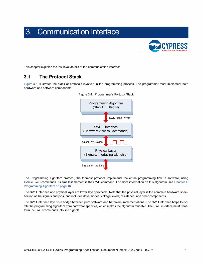
3.1 The Protocol Stack
Figure 3-1 illustrates the stack of protocols involved in the programming process. The programmer must implement bothhardware and software components.
Figure 3-1. Programmer’s Protocol Stack
The Programming Algorithm protocol, the topmost protocol, implements the entire programming flow in software, usingatomic SWD commands. Its smallest element is the SWD command. For more information on this algorithm, see Chapter 4:Programming Algorithm on page 16.
The SWD Interface and physical layer are lower layer protocols. Note that the physical layer is the complete hardware speci-fication of the signals and pins, and includes drive modes, voltage levels, resistance, and other components.
The SWD interface layer is a bridge between pure software and hardware implementations. The SWD interface helps to iso-late the programming algorithm from hardware specifics, which makes the algorithm reusable. The SWD interface must trans-form the SWD commands into line signals.
Programming Algorithm(Step 1 ... Step N)
SWD – Interface(Hardware Access Commands)
Physical Layer(Signals, interfacing with chip)
SWD Read / Write
Logical SWD-signal
Signals on the Line
CYUSB43xx EZ-USB HX3PD Programming Specification, Document Number: 002-27814 Rev. ** 11
Communication Interface
3.2 SWD Interface
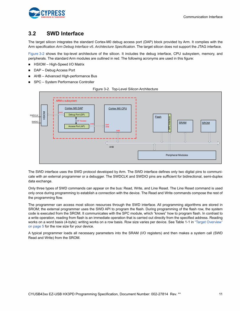
The target silicon integrates the standard Cortex-M0 debug access port (DAP) block provided by Arm. It complies with theArm specification Arm Debug Interface v5. Architecture Specification. The target silicon does not support the JTAG interface.
Figure 3-2 shows the top-level architecture of the silicon. It includes the debug interface, CPU subsystem, memory, andperipherals. The standard Arm modules are outlined in red. The following acronyms are used in this figure:
HSIOM – High-Speed I/O Matrix
DAP – Debug Access Port
AHB – Advanced High-performance Bus
SPC – System Performance Controller
Figure 3-2. Top-Level Silicon Architecture
The SWD interface uses the SWD protocol developed by Arm. The SWD interface defines only two digital pins to communi-cate with an external programmer or a debugger. The SWDCLK and SWDIO pins are sufficient for bidirectional, semi-duplexdata exchange.
Only three types of SWD commands can appear on the bus: Read, Write, and Line Reset. The Line Reset command is usedonly once during programming to establish a connection with the device. The Read and Write commands compose the rest ofthe programming flow.
The programmer can access most silicon resources through the SWD interface. All programming algorithms are stored inSROM; the external programmer uses the SWD API to program the flash. During programming of the flash row, the systemcode is executed from the SROM. It communicates with the SPC module, which “knows” how to program flash. In contrast toa write operation, reading from flash is an immediate operation that is carried out directly from the specified address. Readingworks on a word basis (4-byte); writing works on a row basis. Row size varies per device. See Table 1-1 in “Target Overview”on page 5 for the row size for your device.
A typical programmer loads all necessary parameters into the SRAM (I/O registers) and then makes a system call (SWDRead and Write) from the SROM.
HS
IOM
Cortex M0 DAP
Debug Port (DP)
Access Port (AP)
AP Access
SWDCLK
SWDIO
SWD
Cortex M0 CPU
AHB DAPAHB
ARM s subsystem
AHB
SP
C In
terf
aceFlash
SRAM SROM
Peripheral Modules
AHB
CYUSB43xx EZ-USB HX3PD Programming Specification, Document Number: 002-27814 Rev. ** 12
Communication Interface
3.3 Hardware Access Commands
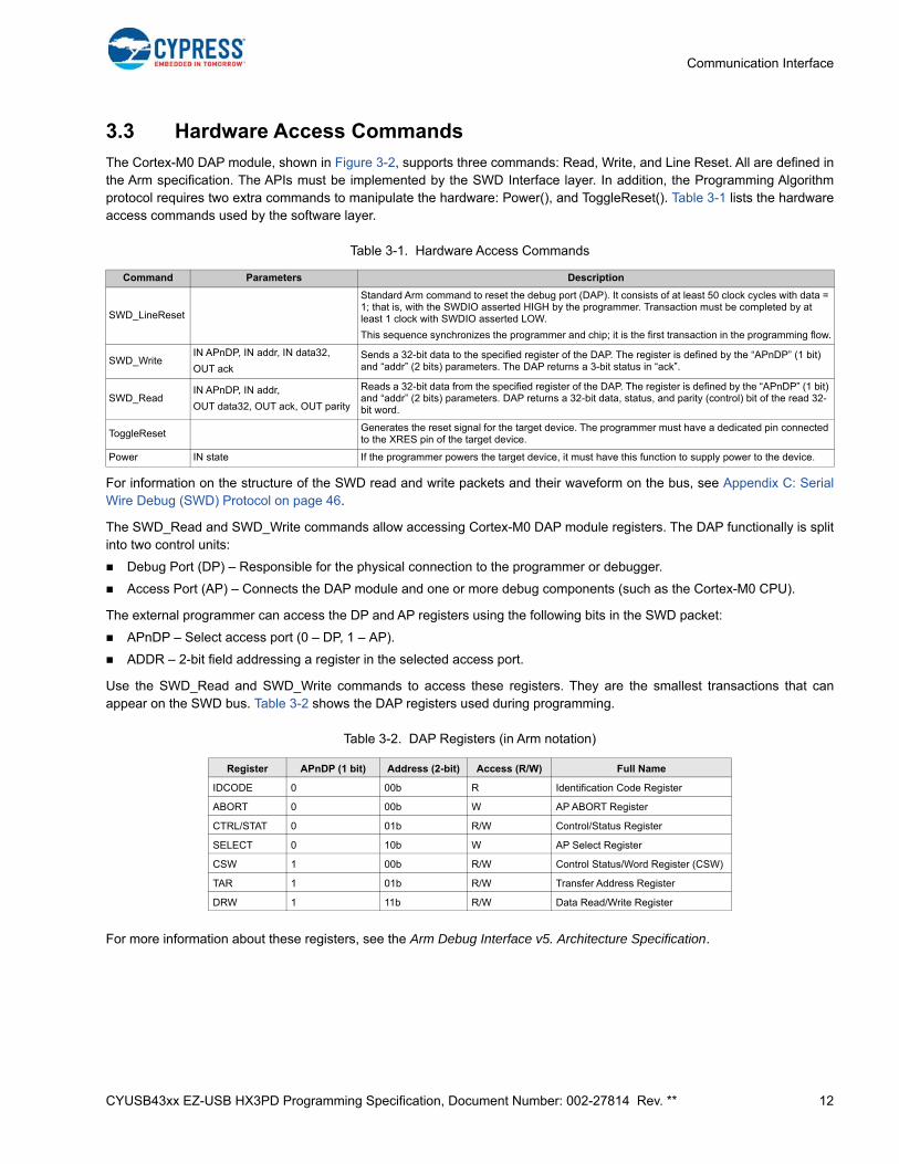
The Cortex-M0 DAP module, shown in Figure 3-2, supports three commands: Read, Write, and Line Reset. All are defined inthe Arm specification. The APIs must be implemented by the SWD Interface layer. In addition, the Programming Algorithmprotocol requires two extra commands to manipulate the hardware: Power(), and ToggleReset(). Table 3-1 lists the hardwareaccess commands used by the software layer.
Table 3-1. Hardware Access Commands
For information on the structure of the SWD read and write packets and their waveform on the bus, see Appendix C: SerialWire Debug (SWD) Protocol on page 46.
The SWD_Read and SWD_Write commands allow accessing Cortex-M0 DAP module registers. The DAP functionally is splitinto two control units:
Debug Port (DP) – Responsible for the physical connection to the programmer or debugger.
Access Port (AP) – Connects the DAP module and one or more debug components (such as the Cortex-M0 CPU).
The external programmer can access the DP and AP registers using the following bits in the SWD packet:
APnDP – Select access port (0 – DP, 1 – AP).
ADDR – 2-bit field addressing a register in the selected access port.
Use the SWD_Read and SWD_Write commands to access these registers. They are the smallest transactions that canappear on the SWD bus. Table 3-2 shows the DAP registers used during programming.
Table 3-2. DAP Registers (in Arm notation)
For more information about these registers, see the Arm Debug Interface v5. Architecture Specification.
Command Parameters Description
SWD_LineReset
Standard Arm command to reset the debug port (DAP). It consists of at least 50 clock cycles with data = 1; that is, with the SWDIO asserted HIGH by the programmer. Transaction must be completed by at least 1 clock with SWDIO asserted LOW.
This sequence synchronizes the programmer and chip; it is the first transaction in the programming flow.
SWD_WriteIN APnDP, IN addr, IN data32,
OUT ackSends a 32-bit data to the specified register of the DAP. The register is defined by the “APnDP” (1 bit) and “addr” (2 bits) parameters. The DAP returns a 3-bit status in “ack”.
SWD_ReadIN APnDP, IN addr,
OUT data32, OUT ack, OUT parity
Reads a 32-bit data from the specified register of the DAP. The register is defined by the “APnDP” (1 bit) and “addr” (2 bits) parameters. DAP returns a 32-bit data, status, and parity (control) bit of the read 32-bit word.
ToggleResetGenerates the reset signal for the target device. The programmer must have a dedicated pin connected to the XRES pin of the target device.
Power IN state If the programmer powers the target device, it must have this function to supply power to the device.
Register APnDP (1 bit) Address (2-bit) Access (R/W) Full Name
IDCODE 0 00b R Identification Code Register
ABORT 0 00b W AP ABORT Register
CTRL/STAT 0 01b R/W Control/Status Register
SELECT 0 10b W AP Select Register
CSW 1 00b R/W Control Status/Word Register (CSW)
TAR 1 01b R/W Transfer Address Register
DRW 1 11b R/W Data Read/Write Register
CYUSB43xx EZ-USB HX3PD Programming Specification, Document Number: 002-27814 Rev. ** 13
Communication Interface
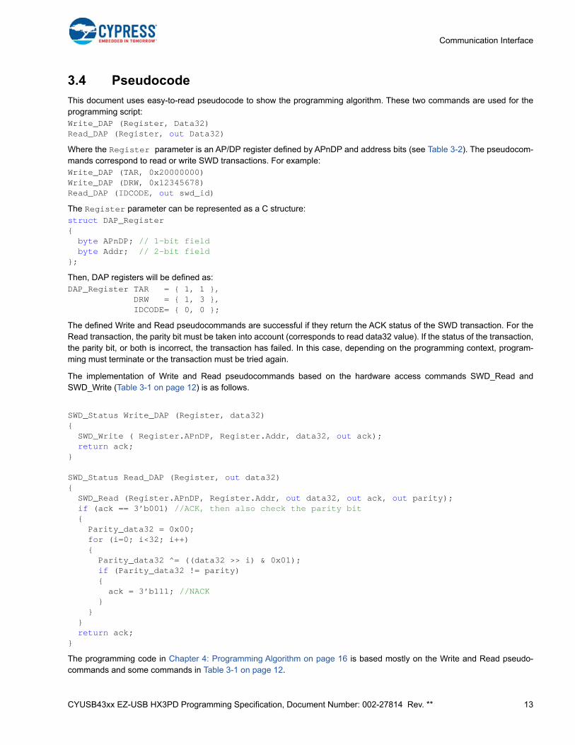
3.4 Pseudocode
This document uses easy-to-read pseudocode to show the programming algorithm. These two commands are used for theprogramming script:Write_DAP (Register, Data32)Read_DAP (Register, out Data32)
Where the Register parameter is an AP/DP register defined by APnDP and address bits (see Table 3-2). The pseudocom-mands correspond to read or write SWD transactions. For example:Write_DAP (TAR, 0x20000000)Write_DAP (DRW, 0x12345678)Read_DAP (IDCODE, out swd_id)
The Register parameter can be represented as a C structure:struct DAP_Register{ byte APnDP; // 1-bit field byte Addr; // 2-bit field};
Then, DAP registers will be defined as:DAP_Register TAR = { 1, 1 }, DRW = { 1, 3 }, IDCODE= { 0, 0 };
The defined Write and Read pseudocommands are successful if they return the ACK status of the SWD transaction. For theRead transaction, the parity bit must be taken into account (corresponds to read data32 value). If the status of the transaction,the parity bit, or both is incorrect, the transaction has failed. In this case, depending on the programming context, program-ming must terminate or the transaction must be tried again.
The implementation of Write and Read pseudocommands based on the hardware access commands SWD_Read andSWD_Write (Table 3-1 on page 12) is as follows.
SWD_Status Write_DAP (Register, data32){
SWD_Write ( Register.APnDP, Register.Addr, data32, out ack);return ack;
}
SWD_Status Read_DAP (Register, out data32){
SWD_Read (Register.APnDP, Register.Addr, out data32, out ack, out parity);if (ack == 3’b001) //ACK, then also check the parity bit
{ Parity_data32 = 0x00;for (i=0; i<32; i++)
{ Parity_data32 ^= ((data32 >> i) & 0x01);
if (Parity_data32 != parity) { ack = 3’b111; //NACK
} } }
return ack;}
The programming code in Chapter 4: Programming Algorithm on page 16 is based mostly on the Write and Read pseudo-commands and some commands in Table 3-1 on page 12.
CYUSB43xx EZ-USB HX3PD Programming Specification, Document Number: 002-27814 Rev. ** 14
Communication Interface
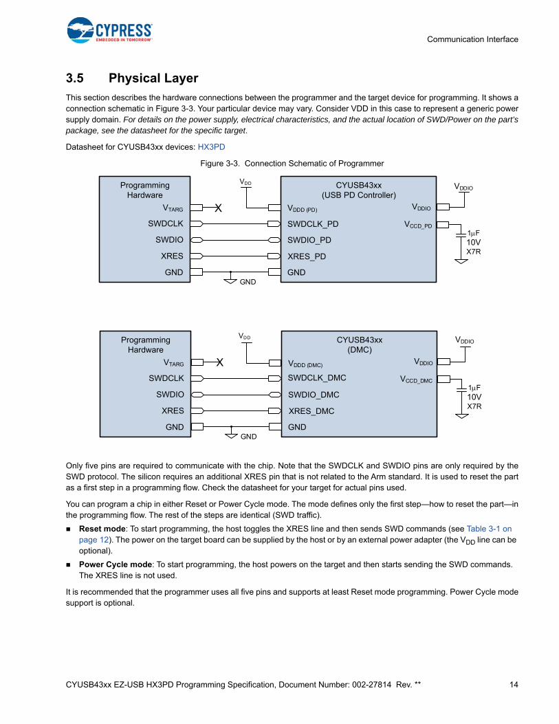
3.5 Physical Layer
This section describes the hardware connections between the programmer and the target device for programming. It shows aconnection schematic in Figure 3-3. Your particular device may vary. Consider VDD in this case to represent a generic powersupply domain. For details on the power supply, electrical characteristics, and the actual location of SWD/Power on the part’spackage, see the datasheet for the specific target.
Datasheet for CYUSB43xx devices: HX3PD
Figure 3-3. Connection Schematic of Programmer
Only five pins are required to communicate with the chip. Note that the SWDCLK and SWDIO pins are only required by theSWD protocol. The silicon requires an additional XRES pin that is not related to the Arm standard. It is used to reset the partas a first step in a programming flow. Check the datasheet for your target for actual pins used.
You can program a chip in either Reset or Power Cycle mode. The mode defines only the first step—how to reset the part—inthe programming flow. The rest of the steps are identical (SWD traffic).
Reset mode: To start programming, the host toggles the XRES line and then sends SWD commands (see Table 3-1 on page 12). The power on the target board can be supplied by the host or by an external power adapter (the VDD line can be optional).
Power Cycle mode: To start programming, the host powers on the target and then starts sending the SWD commands. The XRES line is not used.
It is recommended that the programmer uses all five pins and supports at least Reset mode programming. Power Cycle modesupport is optional.
Programming Hardware
CYUSB43xx(DMC)
VTARG
SWDCLK
XRES
SWDIO
GND
SWDCLK_DMC
XRES_DMC
SWDIO_DMC
GND
VCCD_DMC
VDDIO
1F10VX7R
GND
Programming Hardware
CYUSB43xx(USB PD Controller)
VTARG
SWDCLK
XRES
SWDIO
GND
SWDCLK_PD
XRES_PD
SWDIO_PD
GND
VCCD_PD
VDDIO
1F10VX7R
GND
X
X
VDDD (PD)
VDD VDDIO
VDDIOVDD
VDDD (DMC)
CYUSB43xx EZ-USB HX3PD Programming Specification, Document Number: 002-27814 Rev. ** 15
Communication Interface
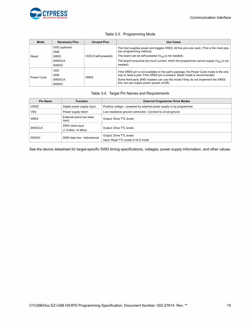
Table 3-3. Programming Mode
Table 3-4. Target Pin Names and Requirements
See the device datasheet for target-specific SWD timing specifications, voltages, power supply information, and other values.
Mode Necessary Pins Unused Pins Use Cases
Reset
VDD (optional)
GND
XRES
SWDCLK
SWDIO
VDD (if self-powered)
The host supplies power and toggles XRES. All five pins are used. (This is the most pop-ular programming method).
The board can be self-powered (VDD is not needed).
The board consumes too much current, which the programmer cannot supply (VDD is not needed).
Power Cycle
VDD
GND
SWDCLK
SWDIO
XRES
If the XRES pin is not available on the part’s package, the Power Cycle mode is the only way to reset a part. If the XRES pin is present, Reset mode is recommended.
Some third-party SWD masters can use this mode if they do not implement the XRES line, but can supply power (power on/off).
Pin Name Function External Programmer Drive Modes
VDDD Digital power supply Input Positive voltage – powered by external power supply or by programmer.
VSS Power supply return Low resistance ground connection. Connect to circuit ground.
XRESExternal active low reset input.
Output: Drive TTL levels
SWDCLKSWD clock input
(1.5 MHz–14 MHz)Output: Drive TTL levels
SWDIO SWD data line - bidirectionalOutput: Drive TTL levels
Input: Read TTL levels in HI-Z mode

CYUSB43xx EZ-USB HX3PD Programming Specification, Document Number: 002-27814 Rev. ** 16
4. Programming Algorithm
This chapter describes in detail the programming flow of the target device. It starts with a high-level description of the algo-rithm and then describes each step using pseudocode. All code is based on subroutines composed of atomic SWD instruc-tions (see “Pseudocode” on page 13). These subroutines are defined in “Subroutines Used in the Programming Flow” onpage 17. The ToggleReset() and Power() routines are also used (see Table 3-1 on page 12).
4.1 High-Level Programming Flow
Figure 4-1 shows the sequence of steps that must be executed to program the target device. The following sections describethese steps in detail. All the steps in this programming flow must be completed successfully for a successful programmingoperation, with the exception of Step 10 Program User SFlash. User SFlash is not present on all targets. Even when present,programming the User SFlash is optional.
The programmer should stop the programming flow if any step fails. In addition, in pseudocode, it is assumed that the pro-grammer checks the status of each SWD transaction (Write_DAP, Read_DAP, WriteIO, ReadIO). This extra code is notshown in the programming script. If any of these transactions fails, then programming must be aborted.
Flash programming is implemented using the SROM APIs. The external programmer puts the parameters into the SRAM (orregisters) and makes system calls, which in turn perform flash updates.
Figure 4-1. High-Level Programming Flow of Target Device
Step 1. Acquire Chip
Step 3. Erase All Flash
Step 4. Checksum Privileged
Step 5. Program Flash
Step 6. Verify Flash
Step 7. Program Protection Settings
Step 8. Verify Protection Settings
Step 9. Verify Checksum
START
FINISH
Step 2. Check Silicon ID
Step 10. Program User SFlash (optional)
CYUSB43xx EZ-USB HX3PD Programming Specification, Document Number: 002-27814 Rev. ** 17
Programming Algorithm
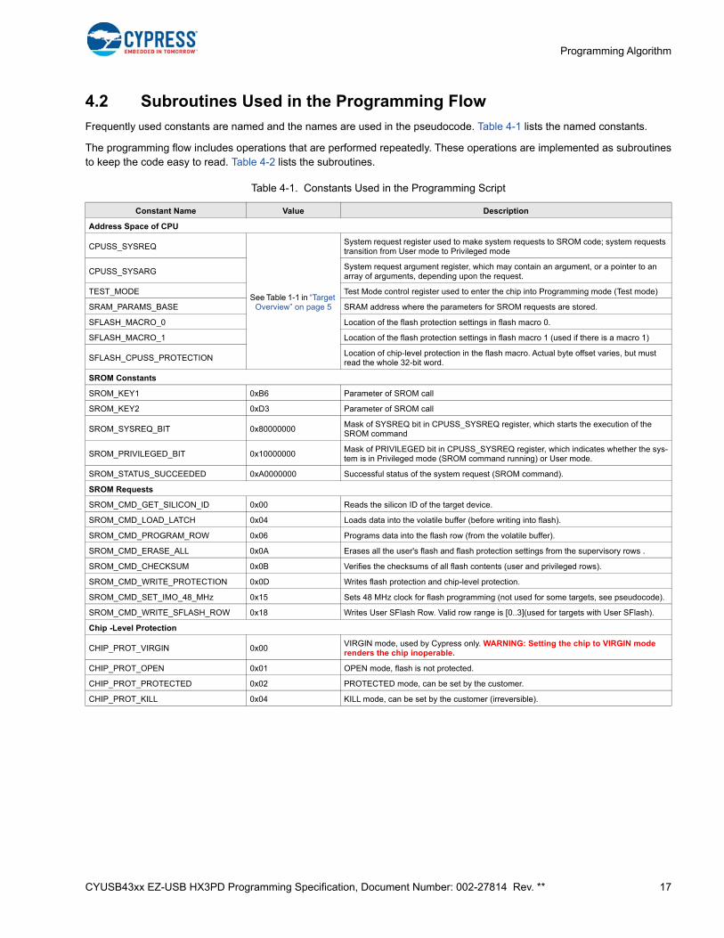
4.2 Subroutines Used in the Programming Flow
Frequently used constants are named and the names are used in the pseudocode. Table 4-1 lists the named constants.
The programming flow includes operations that are performed repeatedly. These operations are implemented as subroutinesto keep the code easy to read. Table 4-2 lists the subroutines.
Table 4-1. Constants Used in the Programming Script
Constant Name Value Description
Address Space of CPU
CPUSS_SYSREQ
See Table 1-1 in “Target Overview” on page 5
System request register used to make system requests to SROM code; system requests transition from User mode to Privileged mode
CPUSS_SYSARGSystem request argument register, which may contain an argument, or a pointer to an array of arguments, depending upon the request.
TEST_MODE Test Mode control register used to enter the chip into Programming mode (Test mode)
SRAM_PARAMS_BASE SRAM address where the parameters for SROM requests are stored.
SFLASH_MACRO_0 Location of the flash protection settings in flash macro 0.
SFLASH_MACRO_1 Location of the flash protection settings in flash macro 1 (used if there is a macro 1)
SFLASH_CPUSS_PROTECTIONLocation of chip-level protection in the flash macro. Actual byte offset varies, but must read the whole 32-bit word.
SROM Constants
SROM_KEY1 0xB6 Parameter of SROM call
SROM_KEY2 0xD3 Parameter of SROM call
SROM_SYSREQ_BIT 0x80000000Mask of SYSREQ bit in CPUSS_SYSREQ register, which starts the execution of the SROM command
SROM_PRIVILEGED_BIT 0x10000000Mask of PRIVILEGED bit in CPUSS_SYSREQ register, which indicates whether the sys-tem is in Privileged mode (SROM command running) or User mode.
SROM_STATUS_SUCCEEDED 0xA0000000 Successful status of the system request (SROM command).
SROM Requests
SROM_CMD_GET_SILICON_ID 0x00 Reads the silicon ID of the target device.
SROM_CMD_LOAD_LATCH 0x04 Loads data into the volatile buffer (before writing into flash).
SROM_CMD_PROGRAM_ROW 0x06 Programs data into the flash row (from the volatile buffer).
SROM_CMD_ERASE_ALL 0x0A Erases all the user's flash and flash protection settings from the supervisory rows .
SROM_CMD_CHECKSUM 0x0B Verifies the checksums of all flash contents (user and privileged rows).
SROM_CMD_WRITE_PROTECTION 0x0D Writes flash protection and chip-level protection.
SROM_CMD_SET_IMO_48_MHz 0x15 Sets 48 MHz clock for flash programming (not used for some targets, see pseudocode).
SROM_CMD_WRITE_SFLASH_ROW 0x18 Writes User SFlash Row. Valid row range is [0..3](used for targets with User SFlash).
Chip -Level Protection
CHIP_PROT_VIRGIN 0x00VIRGIN mode, used by Cypress only. WARNING: Setting the chip to VIRGIN mode renders the chip inoperable.
CHIP_PROT_OPEN 0x01 OPEN mode, flash is not protected.
CHIP_PROT_PROTECTED 0x02 PROTECTED mode, can be set by the customer.
CHIP_PROT_KILL 0x04 KILL mode, can be set by the customer (irreversible).
CYUSB43xx EZ-USB HX3PD Programming Specification, Document Number: 002-27814 Rev. ** 18
Programming Algorithm
Table 4-2. Subroutines Used in Programming Flow
The implementation of these subroutines follows. It is based on the pseudocode and registers defined in “Hardware AccessCommands” on page 12 and “Pseudocode” on page 13. The code uses the constants defined in this chapter. The pseudo-code is similar to C notation.
// WriteIO Subroutinebool “WriteIO” (addr32, data32){ ack1 = Write_DAP (TAR, addr32); ack2 = Write_DAP (DRW, data32); return (ack1 == 3’b001) && (ack2 == 3b’001);}
// “ReadIO” Subroutinebool ReadIO (addr32, OUT data32){ ack1 = Write_DAP (TAR, addr32); ack2 = Read_DAP (DRW, OUT data32); ack3 = Read_DAP (DRW, OUT data32); return (ack1 == 3’b001) && (ack2 == 3b’001) && (ack3 == 3b’001);}
// “PollSROMStatus” Subroutinebool PollSROMStatus(){ do { ReadIO (CPUSS_SYSREQ, OUT status); Status &= (SROM_SYSREQ_BIT | SROM_PRIVILEGED_BIT); }while ((status != 0) && (time_elapsed < 1 sec));
if (time_elapsed >= 1 sec ) return FAIL; // timeout
ReadIO (CPUSS_SYSARG, OUT statusCode); if ((statusCode & 0xF0000000) != (SROM_STATUS_SUCCEEDED)) { return FAIL; // SROM command failed } else return PASS; // SROM command succeeded }}
Subroutine Description
bool WriteIO(addr32, data32)Writes a 32-bit value into the specified address of the CPU address space.
Returns “true” if all SWD transactions succeeded (ACKed).
bool ReadIO(addr32, OUT data 32)
Reads a 32-bit value from the specified address of the CPU address space. Note that the actual size of the read data (8, 16, 32 bits) depends on the setting in the DAP CSW register (see Table 3-2). By default, all accesses are 32 bits long.
Returns “true” if all SWD transactions succeeded (ACKed).
bool PollSROMStatus()Waits until the SROM command is complete and then checks its status. Timeout is 1 second. Returns "true" (suc-cess) if the command is completed and its status is successful; otherwise, returns "false".
CYUSB43xx EZ-USB HX3PD Programming Specification, Document Number: 002-27814 Rev. ** 19
Programming Algorithm
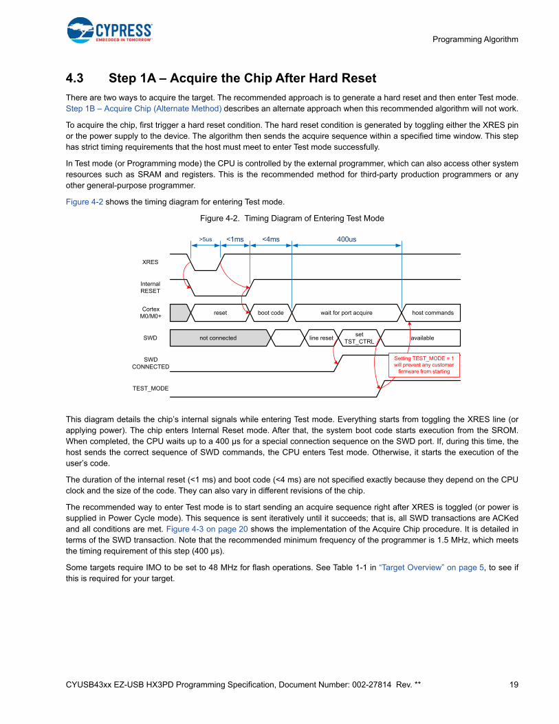
4.3 Step 1A – Acquire the Chip After Hard Reset
There are two ways to acquire the target. The recommended approach is to generate a hard reset and then enter Test mode.Step 1B – Acquire Chip (Alternate Method) describes an alternate approach when this recommended algorithm will not work.
To acquire the chip, first trigger a hard reset condition. The hard reset condition is generated by toggling either the XRES pinor the power supply to the device. The algorithm then sends the acquire sequence within a specified time window. This stephas strict timing requirements that the host must meet to enter Test mode successfully.
In Test mode (or Programming mode) the CPU is controlled by the external programmer, which can also access other systemresources such as SRAM and registers. This is the recommended method for third-party production programmers or anyother general-purpose programmer.
Figure 4-2 shows the timing diagram for entering Test mode.
Figure 4-2. Timing Diagram of Entering Test Mode
This diagram details the chip’s internal signals while entering Test mode. Everything starts from toggling the XRES line (orapplying power). The chip enters Internal Reset mode. After that, the system boot code starts execution from the SROM.When completed, the CPU waits up to a 400 µs for a special connection sequence on the SWD port. If, during this time, thehost sends the correct sequence of SWD commands, the CPU enters Test mode. Otherwise, it starts the execution of theuser’s code.
The duration of the internal reset (<1 ms) and boot code (<4 ms) are not specified exactly because they depend on the CPUclock and the size of the code. They can also vary in different revisions of the chip.
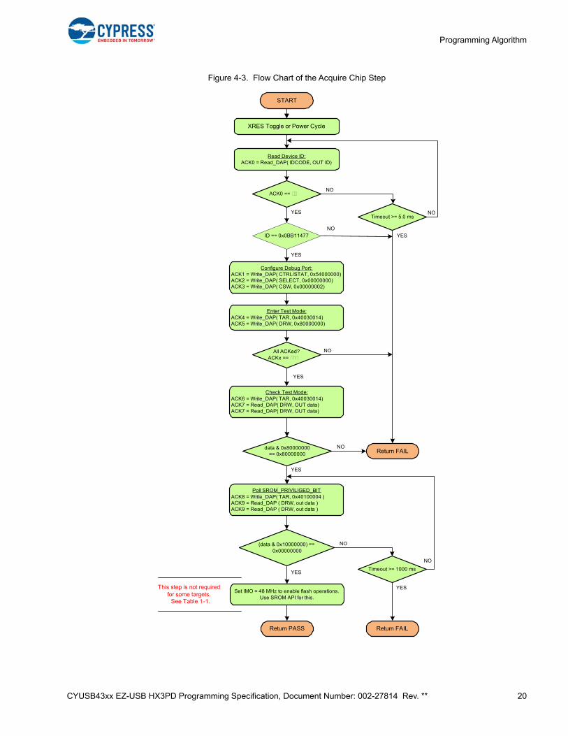
The recommended way to enter Test mode is to start sending an acquire sequence right after XRES is toggled (or power issupplied in Power Cycle mode). This sequence is sent iteratively until it succeeds; that is, all SWD transactions are ACKedand all conditions are met. Figure 4-3 on page 20 shows the implementation of the Acquire Chip procedure. It is detailed interms of the SWD transaction. Note that the recommended minimum frequency of the programmer is 1.5 MHz, which meetsthe timing requirement of this step (400 µs).
Some targets require IMO to be set to 48 MHz for flash operations. See Table 1-1 in “Target Overview” on page 5, to see ifthis is required for your target.
XRES
Internal RESET
reset boot code host commandswait for port acquireCortex
M0/M0+
SWD not connected line reset
SWD CONNECTED
setTST_CTRL
available
TEST_MODE
>5us <1ms <4ms 400us
Setting TEST_MODE = 1 will prevent any customer
firmware from starting
CYUSB43xx EZ-USB HX3PD Programming Specification, Document Number: 002-27814 Rev. ** 20
Programming Algorithm
Figure 4-3. Flow Chart of the Acquire Chip Step
XRES Toggle or Power Cycle
START
Read Device ID:ACK0 = Read_DAP( IDCODE, OUT ID)
ACK0 ==
ID == 0x0BB11477
YES
YES
Timeout >= 5.0 ms
NO
Return FAIL
Configure Debug Port:ACK1 = Write_DAP( CTRL/STAT, 0x54000000)ACK2 = Write_DAP( SELECT, 0x00000000)ACK3 = Write_DAP( CSW, 0x00000002)
Enter Test Mode:ACK4 = Write_DAP( TAR, 0x40030014)ACK5 = Write_DAP( DRW, 0x80000000)
All ACKed?ACKx ==
YES
NO
Check Test Mode:ACK6 = Write_DAP( TAR, 0x40030014)ACK7 = Read_DAP( DRW, OUT data)ACK7 = Read_DAP( DRW, OUT data)
data & 0x80000000 == 0x80000000
YES
NO
Poll SROM_PRIVILIGED_BITACK8 = Write_DAP( TAR, 0x40100004 )ACK9 = Read_DAP ( DRW, out data )ACK9 = Read_DAP ( DRW, out data )
(data & 0x10000000) == 0x00000000
Return PASS
YESTimeout >= 1000 ms
NO
Return FAIL
YES
NO
YES
NO
Set IMO = 48 MHz to enable flash operations. Use SROM API for this.
This step is not required for some targets. See Table 1-1.
NO
CYUSB43xx EZ-USB HX3PD Programming Specification, Document Number: 002-27814 Rev. ** 21
Programming Algorithm
Pseudocode: Step 1A – Acquire Chip
//-------------------------------------------------------------------------------// Reset Target depending on acquire mode – Reset or Power Cycleif (AcquireMode == “Reset”) ToggleXRES(); // Toggle XRES pin, target must be powered.else if (AcquireMode == “Power Cycle”) PowerOn(); // Supply power to target.
// Execute Arm’s connection sequence – acquire SWD-port.do{ SWD_LineReset(); ack = Read_DAP ( IDCODE, out ID);}while ((ack != 3b’001) && time_elapsed < 5.0 ms); //for PowerCycle timeout must be //longer. For example ~30 ms.if (time_elapsed >= 5.0 ms) return FAIL;
// The valid ID value for CM0+ is 0x0BC11477, adjust if necessary for your targetif (ID != 0x0BB11477) return FAIL; // SWD ID
// Initialize Debug PortWrite_DAP (CTRL/STAT, 0x54000000);Write_DAP (SELECT, 0x00000000);Write_DAP (CSW, 0x00000002);
// Enter CPU into Test ModeWriteIO (TEST_MODE, 0x80000000); //Set test_mode bit in TEST_MODE reg from CPU spaceReadIO (TEST_MODE, out status);
if ((status & 0x80000000) != 0x80000000) return FAIL;
// Poll SROM_PRIVILEGED_BIT in CPUSS_SYSREQ registerdo{ ReadIO (CPUSS_SYSREQ, out status); status &= SROM_PRIVILEGED_BIT;} while ((status != 0x00000000) && time_elapsed < 1000 ms)
if (time_elapsed >= 1000 ms) return FAIL;
// The following SROM call is not required for some targets.// Refer to Table 1-1 on page 5 to determine whether this call is required for your device.
// Set "IMO = 48 MHz" to enable Erase/Program/Write Flash operations.Params = (SROM_KEY1 << 0) + //KEY1 ((SROM_KEY2+SROM_CMD_SET_IMO_48MHz) << 8); //KEY2
WriteIO (CPUSS_SYSARG,Params); //Write Params in CPUSS_SYSARGWriteIO (CPUSS_SYSREQ, SROM_SYSREQ_BIT | SROM_CMD_SET_IMO_48MHz); // Request SROM call
status = PollSromStatus();if (!status) return FAIL;return PASS;
CYUSB43xx EZ-USB HX3PD Programming Specification, Document Number: 002-27814 Rev. ** 22
Programming Algorithm
4.4 Step 1B – Acquire Chip (Alternate Method)
There may be cases where the host programmer’s hardware and software constraints prevent programming the device inTest mode. These constraints can include:
Host programmer hardware cannot toggle the XRES pin or the power supply to the target device. Only the SWD protocol pins (SWDIO, SWDCLK) are available for programming.
The host programmer software application cannot meet the timing requirements to enter test mode after triggering a hard reset condition. In such a scenario, the device enters the user code execution mode after the test mode timing window elapses.
For a host programmer with any of the above constraints, this section provides a modified acquire chip sequence that doesnot require XRES/power supply toggling, and which does not have the test mode timing requirements. Only the SWD protocolpins are used for programming. This alternate method only works under the following conditions:
The SWD pins on the target device have not been repurposed. If the SWD pins are repurposed as part of the existing firm-ware image in flash memory, the SWD pins are not available for communication with the host SWD interface to update the existing firmware image.
The chip protection mode of the existing firmware image in the device is set for OPEN mode.
Devices coming from the factory satisfy both the above listed conditions, and can be programmed using the modified acquiresequence listed in this section. If firmware previously programmed into the device does not meet any of the above conditions,then subsequent re-programming of the device is not possible using the modified acquire sequence. Because of this limita-tion, this method is not recommended for third-party programmers or general-purpose programmers, because they arerequired to support programming under all possible operating conditions.
Pseudocode: Step 1B – Acquire Chip (Alternate Method)
//-------------------------------------------------------------------------------// Execute SWD connect sequence.// 100 ms time out below is worst case time out valuedo{ SWD_LineReset(); ack = Read_DAP(IDCODE, out ID);} while((ack != 3b'001) && time_elapsed < 100 ms);
// The valid ID value can be either 0x0BB11477 (CM0) or 0x0BC11477 (CM0+)if (((ID != 0x0BB11477) && (ID != 0x0BC11477)) || (time_elapsed >= 100 ms)) return FAIL;
// Clear WDATAERR if any previous firmware upgrade operation was aborted in the middle// and WDATAERR bit is set. This write is to the AP ABORT register in Debug Port // (APnDP bit - 0, Address is 2'b00, Access - W for the AP ABORT register Write_DAP (ABORT, 0x00000008);
//Set the CSYSPWRUPREQ (System power up request), CDBGPRWUPREQ (Debug power up request),//CDBGRSTREQ (Debug reset request) bits in DP_CTRLSTAT register Write_DAP (CTRL/STAT, 0x54000000);
// Set the AP register bank selection Write_DAP (SELECT, 0x00000000);
// Set the register access as word (4-byte) access // For devices with CM0+ CPU, the HPROT[1] bit also needs to be set along with few// other bit fieldsif (ID == 0x0BC11477) {
CYUSB43xx EZ-USB HX3PD Programming Specification, Document Number: 002-27814 Rev. ** 23
Programming Algorithm
// CM0+ CPU CSW configuration Write_DAP (CSW, 0x03000042);}else{ // CM0 CPU CSW configuration Write_DAP (CSW, 0x00000002);}
// Enable debug, and halt the CPUWriteIO (0xE000EDF0, 0xA05F0003);
// Verify the debug enable, cpu halt bits are setReadIO (0xE000EDF0, out status);if ((status & 0x00000003) != 0x00000003) return FAIL;
// Enable Breakpoint unit WriteIO (0xE0002000, 0x00000003);
// Get address at reset vectorReadIO (0x00000004, out reset_address);
// Map the address bits to the breakpoint compare register// bit map, set the enable breakpoint bit, and the match bitsreset_address = (reset_address & 0x1FFFFFFC) | 0xC0000001;
//Update the breakpoint compare registerWriteIO (0xE0002008, reset_address);
// Issue software resetWriteIO (0xE000ED0C, 0x05FA0004);
// Sufficient delay after reset for boot processDelay(5 ms);
// Repeat a portion of the acquire sequence againdo{ SWD_LineReset(); ack = Read_DAP(IDCODE, out ID);} while ((ack != 3b'001) && time_elapsed < 100 ms);
if (((ID != 0x0BB11477) && (ID != 0x0BC11477))||(time_elapsed >= 100 ms)) return FAIL;
Write_DAP (CTRL/STAT, 0x54000000);Write_DAP (SELECT, 0x00000000);
if (ID == 0x0BC11477) { Write_DAP (CSW, 0x03000042);}else{ Write_DAP (CSW, 0x00000002);}
CYUSB43xx EZ-USB HX3PD Programming Specification, Document Number: 002-27814 Rev. ** 24
Programming Algorithm
// Verify the debug enable, cpu halt bits are setReadIO (0xE000EDF0, out status);if ((status & 0x00000003) != 0x00000003) return FAIL;
// Load infinite for loop code in SRAM address 0x20000300WriteIO (0x20000300, 0xE7FEE7FE);
// Load PC with address of infinite for loop SRAM address with thumb bit (bit 0) setWriteIO (0xE000EDF8, 0x20000301);WriteIO (0xE000EDF4, 0x0001000F);
// Load SP with top of SRAM address - Set for minimum SRAM size devices (2 KB size)WriteIO (0xE000EDF8, 0x20000800);WriteIO (0xE000EDF4, 0x00010011);
// Read xPSR register, set the thumb bit, and restore modified value to xPSR registerWriteIO (0xE000EDF4, 0x00000010);ReadIO (0xE000EDF8, out psr_reg_val);psr_reg_val = psr_reg_val | 0x01000000;WriteIO (0xE000EDF8, psr_reg_val);WriteIO (0xE000EDF4, 0x00010010);
// Disable Breakpoint unitWriteIO (0xE0002000, 0x00000002);
// Unhalt CPUWriteIO (0xE000EDF0, 0xA05F0001);
// The following SROM call is not required for some targets.// Refer to Table 1-1 on page 5 to determine whether this call is required for your device.
// Set "IMO = 48 MHz" to enable Erase/Program/Write Flash operations.Params = (SROM_KEY1 << 0) + //KEY1 ((SROM_KEY2+SROM_CMD_SET_IMO_48MHz) << 8); //KEY2
// Write Params in CPUSS_SYSARG WriteIO (CPUSS_SYSARG,Params);WriteIO (CPUSS_SYSREQ, SROM_SYSREQ_BIT | SROM_CMD_SET_IMO_48MHz); // Request SROM call
status = PollSromStatus();if (!status) return FAIL;
return PASS;//-------------------------------------------------------------------------------
After completing the programming steps from "Acquire Chip" until the programming/verification of nonvolatile memory, thedevice is usually reset to start execution of the programmed firmware. If the host is unable to toggle the XRES pin or powerpin to the target device to perform a reset, a software reset can be triggered by the host through the SWD interface as givenbelow. This should be done at the end of programming operation.
// Issue software resetWriteIO (0xE000ED0C, 0x05FA0004);
CYUSB43xx EZ-USB HX3PD Programming Specification, Document Number: 002-27814 Rev. ** 25
Programming Algorithm
4.5 Step 2 – Check Silicon ID
After acquiring the device, this step verifies that the device corresponds to the hex file. It reads the silicon ID from the hex fileand compares it with the ID obtained from the target.
The silicon ID consists of four bytes:
High byte of the silicon ID
Low byte of the silicon ID
Revision ID (not relevant to device programming)
Family ID
In most cases the combination of the high byte of the silicon ID and the family ID distinguish any device. The low byte of thesilicon ID and the revision ID can be ignored. The pseudocode is written for this general case. However for HX3PD, you mustalso check the low byte of the silicon ID to identify the device.
If your algorithm must distinguish these targets, modify the pseudocode in this step to accommodate this exception.
Pseudocode: Step 2 – Check Silicon ID
//-------------------------------------------------------------------------------// Read “Silicon ID” from hex file, 4 bytes from address 0x9050 0002 (big endian):// HexID[0] - Silicon ID Hi// HexID[1] - Silicon ID Lo// HexID[2] - Revision ID// HexID[3] - Family ID// HEX_ReadSiliconID() must be implemented.
HexID = HEX_ReadSiliconID();
// Read “Silicon ID” from the target using SROM requestParams = (SROM_KEY1 << 0) + //KEY1 ((SROM_KEY2+SROM_CMD_GET_SILICON_ID) << 8); //KEY2
WriteIO (CPUSS_SYSARG, Params); // Write parameters in CPUSS_SYSARTWriteIO (CPUSS_SYSREQ, SROM_SYSREQ_BIT | SROM_CMD_GET_SILICON_ID); // Request SROM callstatus = PollSromStatus();if (!status) return FAIL;
// Read 32-bit ID from the registers// CPUSS_SYSARG[7:0] - Silicon ID Lo// CPUSS_SYSARG[15:8] - Silicon ID Hi// CPUSS_SYSARG[23:16] - Revision ID// CPUSS_SYSREQ[11:0] - Family IDReadIO (CPUSS_SYSARG, out part0);ReadIO (CPUSS_SYSREQ, out part1);
siliconID[0] = (part0 >> 8) & 0xFF; // Silicon ID HisiliconID[1] = (part0 >> 0) & 0xFF; // Silicon ID LosiliconID[2] = (part0 >> 16)& 0xFF; // Revision IDsiliconID[3] = (part1 >> 0) & 0xFF; // Family ID
// Compare IDs from the hex and from the targetfor (i = 0; i < 4; i++){ if (i == 1) continue; if (i == 2) continue; if (siliconID[i] != hexID[i] ) return FAIL;
CYUSB43xx EZ-USB HX3PD Programming Specification, Document Number: 002-27814 Rev. ** 26
Programming Algorithm
}return PASS;
4.6 Step 3 – Erase All Flash
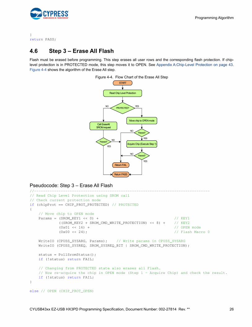
Flash must be erased before programming. This step erases all user rows and the corresponding flash protection. If chip-level protection is in PROTECTED mode, this step moves it to OPEN. See Appendix A:Chip-Level Protection on page 43.Figure 4-4 shows the algorithm of the Erase All step.
Figure 4-4. Flow Chart of the Erase All Step
Pseudocode: Step 3 – Erase All Flash//-------------------------------------------------------------------------------// Read Chip Level Protection using SROM call// Check current protection modeif (chipProt == CHIP_PROT_PROTECTED) // PROTECTED{ // Move chip to OPEN mode Params = (SROM_KEY1 << 0) + // KEY1 ((SROM_KEY2 + SROM_CMD_WRITE_PROTECTION) << 8) + // KEY2 (0x01 << 16) + // OPEN mode (0x00 << 24); // Flash Macro 0
WriteIO (CPUSS_SYSARG, Params); // Write params in CPUSS_SYSARG WriteIO (CPUSS_SYSREQ, SROM_SYSREQ_BIT | SROM_CMD_WRITE_PROTECTION);
status = PollSromStatus(); if (!status) return FAIL; // Changing from PROTECTED state also erases all Flash. // Now re-acquire the chip in OPEN mode (Step 1 - Acquire Chip) and check the result. if (!status) return FAIL;}
else // OPEN (CHIP_PROT_OPEN)
Read Chip Level Protection
START
PROTECTED?
Call EraseAll SROM request
Passed?
Move chip to OPEN mode
Acquire Chip (Execute Step 1)YES
Passed?
YES
Passed?
YES
Return FAIL
Return PASS
NO
NO
NO
NO YES
CYUSB43xx EZ-USB HX3PD Programming Specification, Document Number: 002-27814 Rev. ** 27
Programming Algorithm
{ Params = (SROM_KEY1 << 0) + // KEY1 ((SROM_KEY2+SROM_CMD_ERASE_ALL) << 8); // KEY2 WriteIO (SRAM_PARAMS_BASE + 0x00, Params); // Write params in SRAM WriteIO (CPUSS_SYSARG, SRAM_PARAMS_BASE); // Set location of parameters WriteIO (CPUSS_SYSREQ, SROM_SYSREQ_BIT | SROM_CMD_ERASE_ALL); // Request SROM call
status = PollSromStatus(); if (!status) return FAIL;}return PASS;//-------------------------------------------------------------------------------
4.7 Step 4 – Checksum Privileged
After the user's flash is erased, calculate the checksum of the privileged rows. The Checksum(All) method calculates thechecksum of the combined privileged rows and user rows. After the user's flash is erased, its checksum must be 0x00. At thispoint the checksum method generates the checksum of the privileged rows only.
“Step 9 – Verify Checksum” on page 38 uses this privileged checksum to calculate the users flash checksum. That checksumis calculated according to the following formula:
Checksum_User = Checksum_Step_9 – Checksum_Step_4
An alternate approach to avoid this step is to calculate the checksum of each row individually and add them. However, thisalternate method takes much longer.
Pseudocode: Step 4 – Checksum Privileged
//-------------------------------------------------------------------------------Params = (SROM_KEY1 << 0) + // KEY1 ((SROM_KEY2+SROM_CMD_CHECKSUM) << 8)+ // KEY2 ((0x0000 & 0x00FF) << 16) + // Row ID[7:0] ((0x8000 & 0xFF00) << 16); // Row ID[15:8] – Checksum All(0x8000) WriteIO (CPUSS_SYSARG, Params); // Write params in CPUSS_SYSARGWriteIO (CPUSS_SYSREQ, SROM_SYSREQ_BIT | SROM_CMD_CHECKSUM); // Request SROM call status = PollSromStatus();if (!status) return FAIL;
// Read Checksum from CPUSS_SYSARG registerReadIO (CPUSS_SYSARG, out checksum_all);Checksum_Privileged = (checksum_all & 0x0FFFFFFF); //28-bit checksum
return PASS;//-------------------------------------------------------------------------------
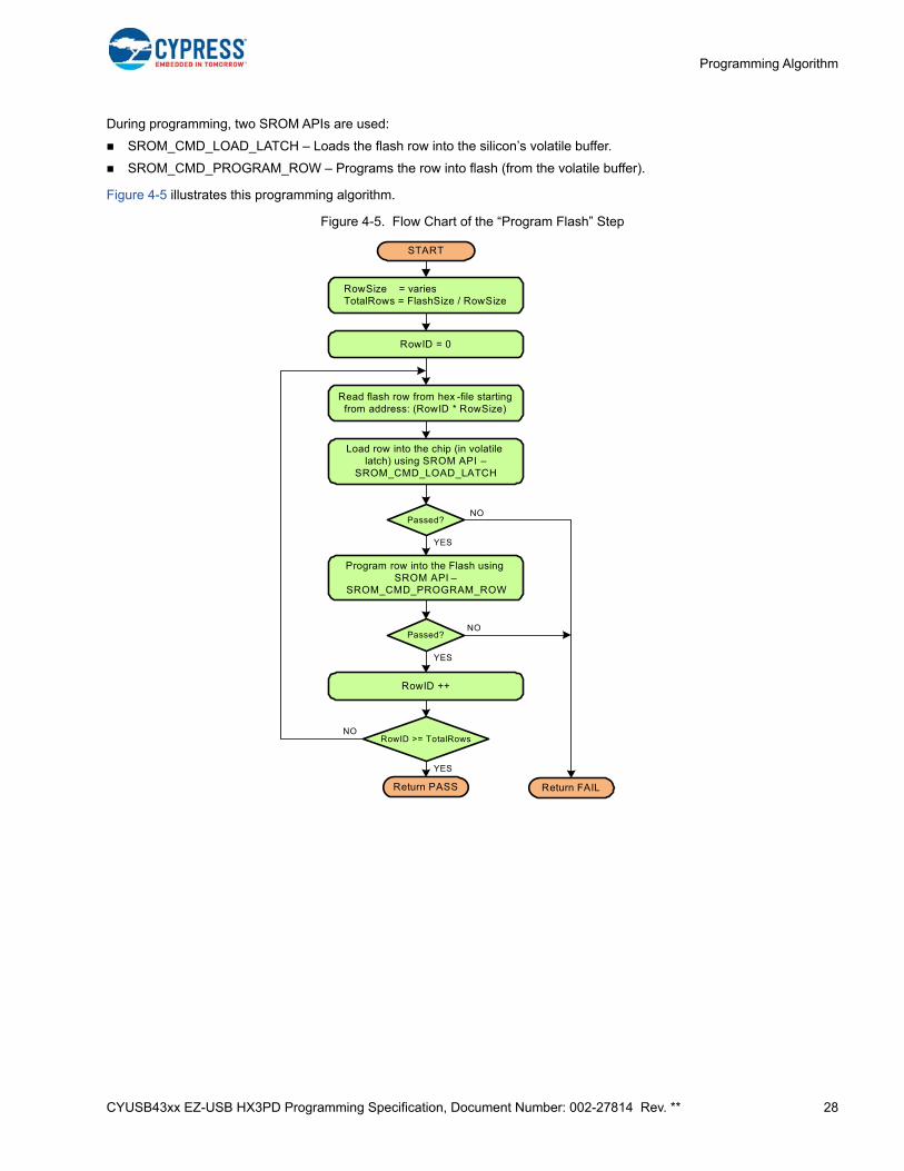
4.8 Step 5 – Program Flash
Flash memory is programmed in rows. The programmer must serially program each row individually. The source data isextracted from the hex file starting from address 0x00000000 (see Figure 2-2 on page 8).
Flash size, row size, and number of rows per macro vary per target. See Table 1-1 in “Target Overview” on page 5, and con-sult the datasheet for your target.
These values are input parameters in this step. Note that the flash size of the acquired silicon must be equal to the size of theuser’s code in the hex file, as verified in Step 2 by comparing the silicon IDs of the hex and the target.
CYUSB43xx EZ-USB HX3PD Programming Specification, Document Number: 002-27814 Rev. ** 28
Programming Algorithm
During programming, two SROM APIs are used:
SROM_CMD_LOAD_LATCH – Loads the flash row into the silicon’s volatile buffer.
SROM_CMD_PROGRAM_ROW – Programs the row into flash (from the volatile buffer).
Figure 4-5 illustrates this programming algorithm.
Figure 4-5. Flow Chart of the “Program Flash” Step
RowSize = varies TotalRows = FlashSize / RowSize
START
RowID = 0
Read flash row from hex -file starting from address: (RowID * RowSize)
Load row into the chip (in volatile latch) using SROM API –
SROM_CMD_LOAD_LATCH
Passed?
Program row into the Flash using SROM API –
SROM_CMD_PROGRAM_ROW
Passed?
RowID ++
RowID >= TotalRowsNO
Return PASS
YES
Return FAIL
NO
NO
YES
YES
CYUSB43xx EZ-USB HX3PD Programming Specification, Document Number: 002-27814 Rev. ** 29
Programming Algorithm
Pseudocode: Step 5 – Program Flash
//-------------------------------------------------------------------------------// Flash Size, Row Size, and Rows per Macro must be provided, and vary per target// FlashSize = 0;// RowSize = 0;// RowsPerMacro = 0;// some targets have only macro 0
TotalRows = FlashSize / RowSize;
// Program all flash rowsfor (int RowID = 0; RowID < TotalRows; RowID++){ // 1. Read Row data from hex RowHexAddress = RowSize * RowID;
// Extract row from the hex-file address "RowHexAddress" into buffer "Data" // HEX_ReadData() must be implemented by Programmer. Data = HEX_ReadData (RowHexAddress, RowSize); // 2. Program a row // Look for the data pattern that causes the SROM API issue // (a non-empty row can be skipped during programming) Checksum = 0; Bits = 0; for (i = 0; i < RowSize; i += 4) { Data32 = (Data[i+3] << 24) + (Data[i + 2] << 16) + (Data[i + 1] << 8) + (Data[i + 0] << 0); Checksum += Data32; Bits |= Data32; }
}return PASS;
//-------------------------------------------------------------------------------// Implementation of ProgramRow() bool ProgramRow (int RowID, byte[] Data, int RowSize){ // Load Row to volatile buffer (latch) MacroID = floor (RowID / RowsPerMacro); // Round down to integer
Params1 = (SROM_KEY1 << 0) + // KEY1 (SROM_KEY2 + SROM_CMD_LOAD_LATCH) << 8) + // KEY2 (0x00 << 16) + // Byte number in latch from what to write (MacroID << 24); // Flash Macro ID (0 or 1)
Params2 = (RowSize - 1); // Number of Bytes to load minus 1
WriteIO (SRAM_PARAMS_BASE + 0x00, Params1); // Write params in SRAM WriteIO (SRAM_PARAMS_BASE + 0x04, Params2); // Write params in SRAM
// Put row data into SRAM buffer for (i = 0; i < RowSize; i += 4) { Params1 = (Data[i] << 0) + (Data[i + 1] << 8) +
CYUSB43xx EZ-USB HX3PD Programming Specification, Document Number: 002-27814 Rev. ** 30
Programming Algorithm
{Data[i + 2] << 16) + (Data[i + 3] << 24); WriteIO (SRAM_PARAMS_BASE + 0x08 + i, Params1); // Write params in SRAM }
// Call "Load Latch" SROM API WriteIO (CPUSS_SYSARG, SRAM_PARAMS_BASE); // Set location of parameters WriteIO (CPUSS_SYSREQ, SROM_SYSREQ_BIT | SROM_CMD_LOAD_LATCH); // SROM operation
Status = PollSromStatus(); if (!Status) return FAIL; // Program Row - call SROM API Params = (SROM_KEY1 << 0) + // KEY1 ((SROM_KEY2+SROM_CMD_PROGRAM_ROW) << 8) + // KEY2 ((RowID & 0x00FF) << 16) + // ROW_ID_LOW[7:0] ((RowID & 0xFF00) << 16); // ROW_ID_HIGH[15:8]
WriteIO (SRAM_PARAMS_BASE+0x00, Params); // Write params in SRAM WriteIO (CPUSS_SYSARG, SRAM_PARAMS_BASE); // Set location of parameters WriteIO (CPUSS_SYSREQ, SROM_SYSREQ_BIT | SROM_CMD_PROGRAM_ROW); // SROM operation
Status = PollSromStatus(); if (!Status) return FAIL; return PASS;}//-------------------------------------------------------------------------------
CYUSB43xx EZ-USB HX3PD Programming Specification, Document Number: 002-27814 Rev. ** 31
Programming Algorithm
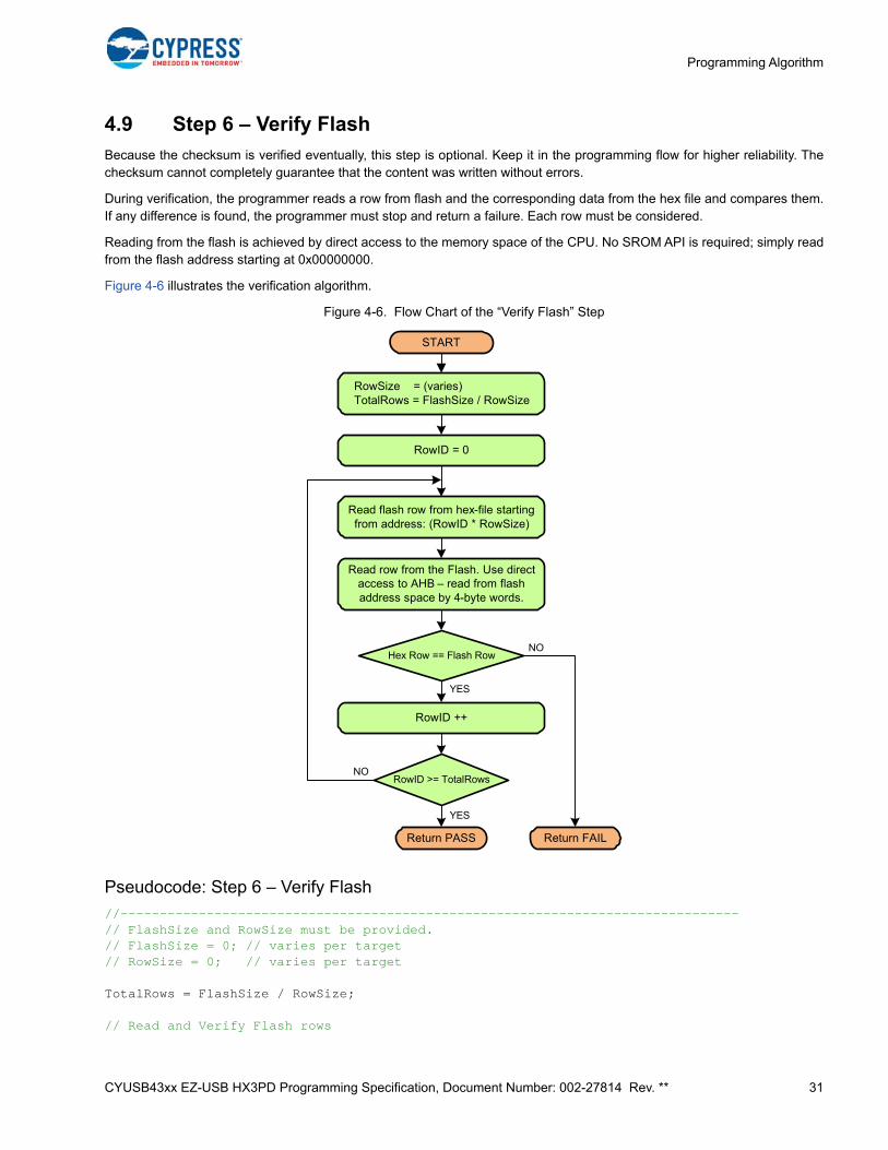
4.9 Step 6 – Verify Flash
Because the checksum is verified eventually, this step is optional. Keep it in the programming flow for higher reliability. Thechecksum cannot completely guarantee that the content was written without errors.
During verification, the programmer reads a row from flash and the corresponding data from the hex file and compares them.If any difference is found, the programmer must stop and return a failure. Each row must be considered.
Reading from the flash is achieved by direct access to the memory space of the CPU. No SROM API is required; simply readfrom the flash address starting at 0x00000000.
Figure 4-6 illustrates the verification algorithm.
Figure 4-6. Flow Chart of the “Verify Flash” Step
Pseudocode: Step 6 – Verify Flash
//-------------------------------------------------------------------------------// FlashSize and RowSize must be provided.// FlashSize = 0; // varies per target// RowSize = 0; // varies per target
TotalRows = FlashSize / RowSize;
// Read and Verify Flash rows
RowSize = (varies) TotalRows = FlashSize / RowSize
START
RowID = 0
Read flash row from hex-file starting from address: (RowID * RowSize)
Read row from the Flash. Use direct access to AHB – read from flash address space by 4-byte words.
Hex Row == Flash Row
RowID ++
Return PASS Return FAIL
RowID >= TotalRowsNO
YES
YES
NO
CYUSB43xx EZ-USB HX3PD Programming Specification, Document Number: 002-27814 Rev. ** 32
Programming Algorithm
for (int RowID = 0; RowID < TotalRows; RowID++){ // 1. Read row from hex file RowAddress = rowSize * rowID; //liner address of row in flash // Extract row from the hex-file address into buffer "hexData" // HEX_ReadData() must be implemented by Programmer hexData = HEX_ReadData(RowAddress, RowSize);
// 2. Read row from chip for (i = 0; i < RowSize; i += 4) { // Read flash via AHB-interface ReadIO (RowAddress + i, out data32); chipData[i + 0] = (data32 >> 0) & 0xFF; chipData[i + 1] = (data32 >> 8) & 0xFF; chipData[i + 2] = (data32 >> 16) & 0xFF; chipData[i + 3] = (data32 >> 24) & 0xFF; }
// 3. Compare them for (i = 0; i < RowSize; i++) { if (chipData[i] != hexData[i]) return FAIL; }}return PASS;//-------------------------------------------------------------------------------
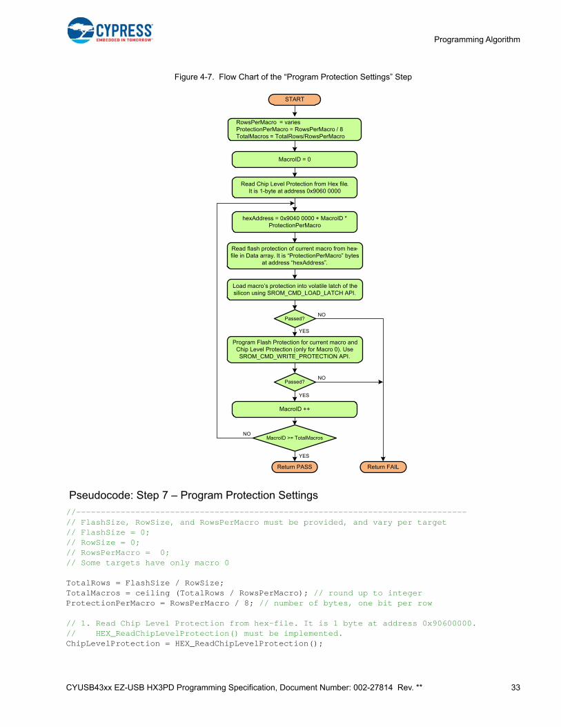
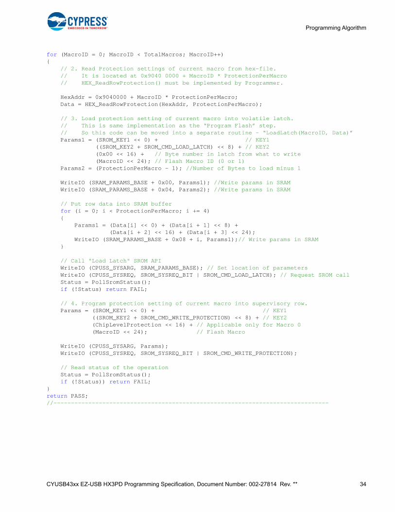
4.10 Step 7 – Program Protection Settings
At this point, the programmer writes into the supervisory flash all protection data: row-level protection and chip-level protec-tion. For more information, see Figure 2-1 on page 7.
Flash size, row size, rows per macro, the number of macros, and the address range of protection data can vary per target.See Table 1-1 in “Target Overview” on page 5 and the datasheet for your target. For example the target device may have twoflash macros, each with its own supervisory rows to store the protection settings of the user’s rows. If your target has only onemacro, it is considered macro 0 for purposes of this algorithm.
Each user row occupies one bit in the protection space: 0 means unprotected; 1 means protected. This provides write/eraseprotection for the row. In the PROTECTED state, a row cannot be erased or written either by the firmware or by an externalprogrammer. The protection setting can be reset only by the EraseAll() operation in Step 3, driven by the external program-mer.
Chip-level protection is only 1 byte and is stored in the supervisory row of macro 0 where the flash protection data resides.
Figure 4-7 shows the algorithm for writing protection settings. It assumes the target has two macros.
CYUSB43xx EZ-USB HX3PD Programming Specification, Document Number: 002-27814 Rev. ** 33
Programming Algorithm
Figure 4-7. Flow Chart of the “Program Protection Settings” Step
Pseudocode: Step 7 – Program Protection Settings
//-------------------------------------------------------------------------------// FlashSize, RowSize, and RowsPerMacro must be provided, and vary per target// FlashSize = 0;// RowSize = 0;// RowsPerMacro = 0; // Some targets have only macro 0
TotalRows = FlashSize / RowSize;TotalMacros = ceiling (TotalRows / RowsPerMacro); // round up to integerProtectionPerMacro = RowsPerMacro / 8; // number of bytes, one bit per row
// 1. Read Chip Level Protection from hex-file. It is 1 byte at address 0x90600000.// HEX_ReadChipLevelProtection() must be implemented. ChipLevelProtection = HEX_ReadChipLevelProtection();
START
RowsPerMacro = varies ProtectionPerMacro = RowsPerMacro / 8 TotalMacros = TotalRows/RowsPerMacro
MacroID = 0
Read Chip Level Protection from Hex file. It is 1-byte at address 0x9060 0000
hexAddress = 0x9040 0000 + MacroID * ProtectionPerMacro
Read flash protection of current macro from hex-file in Data array. It is “ProtectionPerMacro” bytes
at address “hexAddress”.
Load macro’s protection into volatile latch of the silicon using SROM_CMD_LOAD_LATCH API.
Passed?
Program Flash Protection for current macro and Chip Level Protection (only for Macro 0). Use SROM_CMD_WRITE_PROTECTION API.
Passed?
MacroID ++
MacroID >= TotalMacros
Return PASS Return FAIL
YES
YES
YES
NO
NO
NO
CYUSB43xx EZ-USB HX3PD Programming Specification, Document Number: 002-27814 Rev. ** 34
Programming Algorithm
for (MacroID = 0; MacroID < TotalMacros; MacroID++){ // 2. Read Protection settings of current macro from hex-file. // It is located at 0x9040 0000 + MacroID * ProtectionPerMacro // HEX_ReadRowProtection() must be implemented by Programmer.
HexAddr = 0x9040000 + MacroID * ProtectionPerMacro; Data = HEX_ReadRowProtection(HexAddr, ProtectionPerMacro);
// 3. Load protection setting of current macro into volatile latch. // This is same implementation as the “Program Flash” step. // So this code can be moved into a separate routine – “LoadLatch(MacroID, Data)” Params1 = (SROM_KEY1 << 0) + // KEY1 ((SROM_KEY2 + SROM_CMD_LOAD_LATCH) << 8) + // KEY2 (0x00 << 16) + // Byte number in latch from what to write (MacroID << 24); // Flash Macro ID (0 or 1) Params2 = (ProtectionPerMacro - 1); //Number of Bytes to load minus 1
WriteIO (SRAM_PARAMS_BASE + 0x00, Params1); //Write params in SRAM WriteIO (SRAM_PARAMS_BASE + 0x04, Params2); //Write params in SRAM
// Put row data into SRAM buffer for (i = 0; i < ProtectionPerMacro; i += 4) { Params1 = (Data[i] << 0) + (Data[i + 1] << 8) + (Data[i + 2] << 16) + (Data[i + 3] << 24); WriteIO (SRAM_PARAMS_BASE + 0x08 + i, Params1);// Write params in SRAM }
// Call "Load Latch" SROM API WriteIO (CPUSS_SYSARG, SRAM_PARAMS_BASE); // Set location of parameters WriteIO (CPUSS_SYSREQ, SROM_SYSREQ_BIT | SROM_CMD_LOAD_LATCH); // Request SROM call Status = PollSromStatus(); if (!Status) return FAIL;
// 4. Program protection setting of current macro into supervisory row. Params = (SROM_KEY1 << 0) + // KEY1 ((SROM_KEY2 + SROM_CMD_WRITE_PROTECTION) << 8) + // KEY2 (ChipLevelProtection << 16) + // Applicable only for Macro 0 (MacroID << 24); // Flash Macro
WriteIO (CPUSS_SYSARG, Params); WriteIO (CPUSS_SYSREQ, SROM_SYSREQ_BIT | SROM_CMD_WRITE_PROTECTION);
// Read status of the operation Status = PollSromStatus(); if (!Status)) return FAIL;}return PASS;//-------------------------------------------------------------------------------
CYUSB43xx EZ-USB HX3PD Programming Specification, Document Number: 002-27814 Rev. ** 35
Programming Algorithm
4.11 Step 8 – Verify Protection Settings
This step verifies the data that was written in Step 7. Simply read back the details of flash protection and chip-level protectionfrom the silicon and compare this with the corresponding data from the hex file. Although this step is optional, Cypress recom-mends that you implement it in the programmer.
Flash size, row size, rows per macro, the number of macros, and the address range of protection data can vary per target.See Table 1-1 in “Target Overview” on page 5 and the datasheet for your target. For example the target device may have twoflash macros, each with its own supervisory rows to store the protection settings of the user’s rows. If your target has only onemacro, it is considered macro 0 for purposes of this algorithm.
Read the protection setting by directly accessing the memory space of the CPU (via AHB). The programmer reads out thedata in 4-byte words.
Note that when a chip-level protection byte is read from the silicon, it must be reviewed. In OPEN and VIRGIN modes, thevalue written in the supervisory rows is inverted when stored in Flash. (See Appendix A:Chip-Level Protection on page 43).For KILL and PROTECTED modes, no translation is necessary.
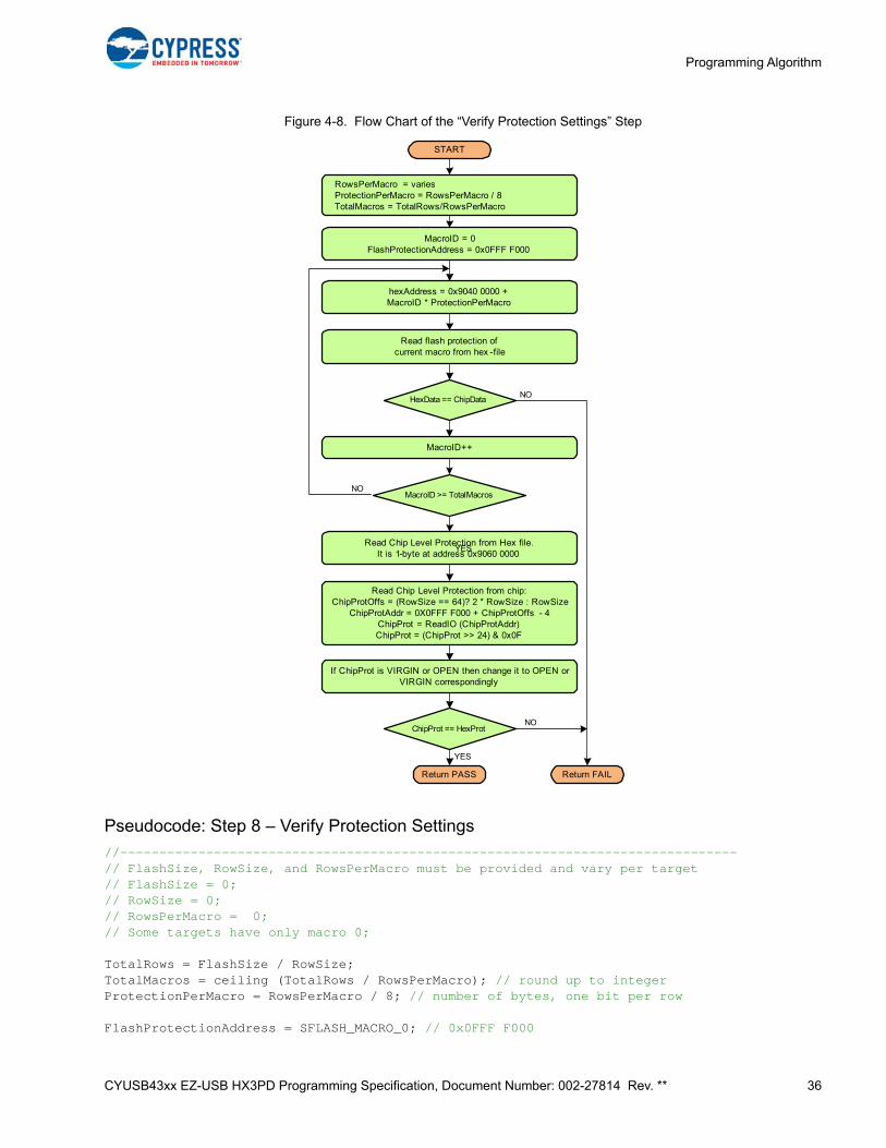
CYUSB43xx EZ-USB HX3PD Programming Specification, Document Number: 002-27814 Rev. ** 36
Programming Algorithm
Figure 4-8. Flow Chart of the “Verify Protection Settings” Step
Pseudocode: Step 8 – Verify Protection Settings
//-------------------------------------------------------------------------------// FlashSize, RowSize, and RowsPerMacro must be provided and vary per target// FlashSize = 0;// RowSize = 0;// RowsPerMacro = 0;// Some targets have only macro 0;
TotalRows = FlashSize / RowSize;TotalMacros = ceiling (TotalRows / RowsPerMacro); // round up to integerProtectionPerMacro = RowsPerMacro / 8; // number of bytes, one bit per row
FlashProtectionAddress = SFLASH_MACRO_0; // 0x0FFF F000
START
RowsPerMacro = variesProtectionPerMacro = RowsPerMacro / 8TotalMacros = TotalRows/RowsPerMacro
MacroID = 0FlashProtectionAddress = 0x0FFF F000
Read flash protection of current macro from hex -file
hexAddress = 0x9040 0000 + MacroID * ProtectionPerMacro
HexData == ChipData
MacroID >= TotalMacros
Read Chip Level Protection from Hex file. It is 1-byte at address 0x9060 0000
YES
NO
YES
Return FAIL
Read Chip Level Protection from chip:ChipProtOffs = (RowSize == 64)? 2 * RowSize : RowSize
ChipProtAddr = 0X0FFF F000 + ChipProtOffs - 4ChipProt = ReadIO (ChipProtAddr)ChipProt = (ChipProt >> 24) & 0x0F
If ChipProt is VIRGIN or OPEN then change it to OPEN or VIRGIN correspondingly
ChipProt == HexProt
Return PASS
YES
NO
NO
MacroID++
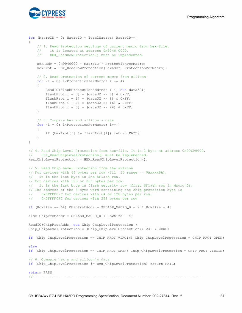
CYUSB43xx EZ-USB HX3PD Programming Specification, Document Number: 002-27814 Rev. ** 37
Programming Algorithm
for (MacroID = 0; MacroID < TotalMacros; MacroID++){ // 1. Read Protection settings of current macro from hex-file. // It is located at address 0x9040 0000. // HEX_ReadRowProtection() must be implemented.
HexAddr = 0x9040000 + MacroID * ProtectionPerMacro; hexProt = HEX_ReadRowProtection(HexAddr, ProtectionPerMacro);
// 2. Read Protection of current macro from silicon for (i = 0; i<ProtectionPerMacro; i += 4) { ReadIO(FlashProtectionAddress + i, out data32); flashProt[i + 0] = (data32 >> 0) & 0xFF; flashProt[i + 1] = (data32 >> 8) & 0xFF; flashProt[i + 2] = (data32 >> 16) & 0xFF; flashProt[i + 3] = (data32 >> 24) & 0xFF; }
// 3. Compare hex and silicon's data for (i = 0; i<ProtectionPerMacro; i++ ) { if (hexProt[i] != flashProt[i]) return FAIL; }}
// 4. Read Chip Level Protection from hex-file. It is 1 byte at address 0x90600000.// HEX_ReadChipLevelProtection() must be implemented. Hex_ChipLevelProtection = HEX_ReadChipLevelProtection();
// 5. Read Chip Level Protection from the silicon// For devices with 64 bytes per row (Sil. ID range == 0Axxxx9A), // it is the last byte in 2nd SFlash row.// For devices with 128 or 256 bytes per row, // it is the last byte in flash security row (first SFlash row in Macro 0).// The address of the 4-byte word containing the chip protection byte is // 0x0FFFF07C for devices with 64 or 128 bytes per row.// 0x0FFFF0FC for devices with 256 bytes per row
if (RowSize == 64) ChipProtAddr = SFLASH_MACRO_0 + 2 * RowSize - 4;
else ChipProtAddr = SFLASH_MACRO_0 + RowSize - 4;
ReadIO(ChipProtAddr, out Chip_ChipLevelProtection);Chip_ChipLevelProtection = (Chip_ChipLevelProtection>> 24) & 0x0F;
if (Chip_ChipLevelProtection == CHIP_PROT_VIRGIN) Chip_ChipLevelProtection = CHIP_PROT_OPEN;
elseif (Chip_ChipLevelProtection == CHIP_PROT_OPEN) Chip_ChipLevelProtection = CHIP_PROT_VIRGIN;
// 6. Compare hex's and silicon's data if (Chip_ChipLevelProtection != Hex_ChipLevelProtection) return FAIL;
return PASS;//-------------------------------------------------------------------------------
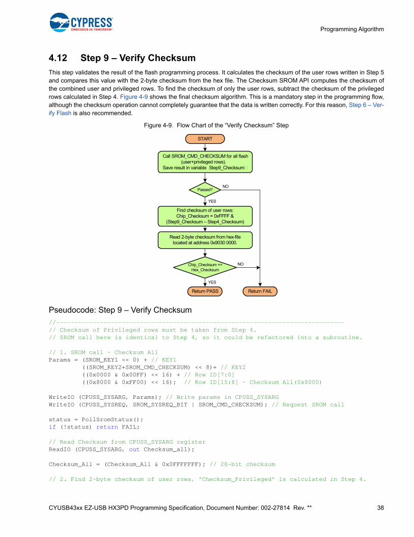
CYUSB43xx EZ-USB HX3PD Programming Specification, Document Number: 002-27814 Rev. ** 38
Programming Algorithm
4.12 Step 9 – Verify Checksum
This step validates the result of the flash programming process. It calculates the checksum of the user rows written in Step 5and compares this value with the 2-byte checksum from the hex file. The Checksum SROM API computes the checksum ofthe combined user and privileged rows. To find the checksum of only the user rows, subtract the checksum of the privilegedrows calculated in Step 4. Figure 4-9 shows the final checksum algorithm. This is a mandatory step in the programming flow,although the checksum operation cannot completely guarantee that the data is written correctly. For this reason, Step 6 – Ver-ify Flash is also recommended.
Figure 4-9. Flow Chart of the “Verify Checksum” Step
Pseudocode: Step 9 – Verify Checksum
//-------------------------------------------------------------------------------// Checksum of Privileged rows must be taken from Step 4.// SROM call here is identical to Step 4, so it could be refactored into a subroutine.
// 1. SROM call - Checksum AllParams = (SROM_KEY1 << 0) + // KEY1 ((SROM_KEY2+SROM_CMD_CHECKSUM) << 8)+ // KEY2 ((0x0000 & 0x00FF) << 16) + // Row ID[7:0] ((0x8000 & 0xFF00) << 16); // Row ID[15:8] - Checksum All(0x8000)
WriteIO (CPUSS_SYSARG, Params); // Write params in CPUSS_SYSARGWriteIO (CPUSS_SYSREQ, SROM_SYSREQ_BIT | SROM_CMD_CHECKSUM); // Request SROM call
status = PollSromStatus();if (!status) return FAIL;
// Read Checksum from CPUSS_SYSARG registerReadIO (CPUSS_SYSARG, out Checksum_all);
Checksum_All = (Checksum_All & 0x0FFFFFFF); // 28-bit checksum
// 2. Find 2-byte checksum of user rows, "Checksum_Privileged" is calculated in Step 4.
START
Call SROM_CMD_CHECKSUM for all flash (user+privileged rows). Save result in variable Step9_Checksum
Find checksum of user rows:Chip_Checksum = 0xFFFF &
(Step9_Checksum – Step4_Checksum)
Read 2-byte checksum from hex-file located at address 0x9030 0000.
Chip_Checksum == Hex_Checksum
Return PASS
YES
Return FAIL
Passed?
YES
NO
NO
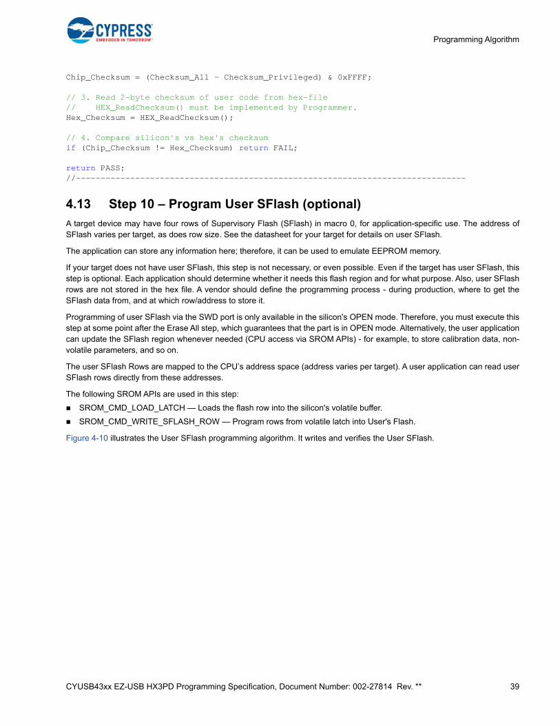
CYUSB43xx EZ-USB HX3PD Programming Specification, Document Number: 002-27814 Rev. ** 39
Programming Algorithm
Chip_Checksum = (Checksum_All - Checksum_Privileged) & 0xFFFF;
// 3. Read 2-byte checksum of user code from hex-file// HEX_ReadChecksum() must be implemented by Programmer.Hex_Checksum = HEX_ReadChecksum();
// 4. Compare silicon's vs hex's checksumif (Chip_Checksum != Hex_Checksum) return FAIL;
return PASS;//-------------------------------------------------------------------------------
4.13 Step 10 – Program User SFlash (optional)
A target device may have four rows of Supervisory Flash (SFlash) in macro 0, for application-specific use. The address ofSFlash varies per target, as does row size. See the datasheet for your target for details on user SFlash.
The application can store any information here; therefore, it can be used to emulate EEPROM memory.
If your target does not have user SFlash, this step is not necessary, or even possible. Even if the target has user SFlash, thisstep is optional. Each application should determine whether it needs this flash region and for what purpose. Also, user SFlashrows are not stored in the hex file. A vendor should define the programming process - during production, where to get theSFlash data from, and at which row/address to store it.
Programming of user SFlash via the SWD port is only available in the silicon's OPEN mode. Therefore, you must execute thisstep at some point after the Erase All step, which guarantees that the part is in OPEN mode. Alternatively, the user applicationcan update the SFlash region whenever needed (CPU access via SROM APIs) - for example, to store calibration data, non-volatile parameters, and so on.
The user SFlash Rows are mapped to the CPU’s address space (address varies per target). A user application can read userSFlash rows directly from these addresses.
The following SROM APIs are used in this step:
SROM_CMD_LOAD_LATCH — Loads the flash row into the silicon's volatile buffer.
SROM_CMD_WRITE_SFLASH_ROW — Program rows from volatile latch into User's Flash.
Figure 4-10 illustrates the User SFlash programming algorithm. It writes and verifies the User SFlash.
CYUSB43xx EZ-USB HX3PD Programming Specification, Document Number: 002-27814 Rev. ** 40
Programming Algorithm
Figure 4-10. Flow Chart of "Program User SFlash" Step
Pseudocode: Step 10 – Program User SFlash
//-------------------------------------------------------------------------------// TotalRows, RowSize, and SFlashAddress must be provided, and vary per target.// TotalRows is the number of SFlash rows// RowSize = 0;// SFlashAddress = 0x00000000;
TotalRows = 4; // check the datasheet for your device
// Program all User SFlash rowsfor (int RowID = 0; RowID < TotalRows; RowID++){ // 1. Prepare data for current row, read it in the "Data" array. // SFlash_ReadSource() must return data for current SFlash row. Data = SFlash_ReadSource(RowID, RowSize);
// 2. Load Row to volatile buffer (latch) MacroID = 0x00; // User SFLash rows are located only in Macro 0
START
RowID = 0
Prepare Data for Current Row ID (row size varies)
Write Data using SROM APIs:SROM_CMD_LOAD_LATCH,
SROM_CMD_WRITE_SFLASH_ROW
Passed?
YES
NO
RowID ++
RowID < TotalRowsYES
RowID = 0
Read a row from SFlash(step through rows)
Flash Row == Source Row
YES
NO
RowID ++
RowID < TotalRows
NO
YES
Return PASS Return FAIL
NO
CYUSB43xx EZ-USB HX3PD Programming Specification, Document Number: 002-27814 Rev. ** 41
Programming Algorithm
Params1 = (SROM_KEY1 << 0) + // KEY1 ((SROM_KEY2 + SROM_CMD_LOAD_LATCH) << 8) + // KEY2 (0x00 << 16) + // Start address (byte number) in the page latch (MacroID << 24); // Flash Macro ID (always zero for this step) Params2 = (RowSize - 1); // Number of Bytes to load minus 1
WriteIO (SRAM_PARAMS_BASE + 0x00, Params1); // Write params in SRAM WriteIO (SRAM_PARAMS_BASE + 0x04, Params2); // Write params in SRAM
// Put row data into SRAM buffer for (i = 0; i < RowSize; i += 4) { Params1 = (Data[i] << 0) + (Data[i + 1 )<< 8) + Data[i + 2] << 16) + (Data[i + 3] << 24); WriteIO (SRAM_PARAMS_BASE + 0x08 + i, Params1); // Write params in SRAM }
// Call "Load Latch" SROM API WriteIO (CPUSS_SYSARG, SRAM_PARAMS_BASE); // Set location of parameters WriteIO (CPUSS_SYSREQ, SROM_SYSREQ_BIT | SROM_CMD_LOAD_LATCH); // Request SROM call
Status = PollSromStatus(); if (!Status) return FAIL;
// 3. Program User SFlash Row - call SROM API Params1 =(SROM_KEY1 << 0) + // KEY1 ((SROM_KEY2+SROM_CMD_WRITE_SFLASH_ROW) << 8); // KEY2
Params2 = RowID // Row ID of User SFlash
WriteIO (SRAM_PARAMS_BASE+0x00, Params1); // Write params in SRAM WriteIO (SRAM_PARAMS_BASE+0x04, Params2); // Write params in SRAM
WriteIO (CPUSS_SYSARG, SRAM_PARAMS_BASE); // Set location of parameters // Request SROM call WriteIO (CPUSS_SYSREQ, SROM_SYSREQ_BIT | SROM_CMD_WRITE_SFLASH_ROW); Status = PollSromStatus(); if (!Status) return FAIL;}
// Verify all User SFlash rowsfor (int RowID = 0; RowID < TotalRows; RowID++){ // 1. Prepare Source data for current row sourceData = SFlash_ReadSource(RowID, RowSize);
// 2. Read row from chip RowAddress = SFlashAddress + RowID * RowSize;
for (i = 0; i < RowSize; i += 4) { // Read flash via AHB-interface ReadIO(RowAddress + i, out data32); chipData[i + 0] = (data32 >> 0) & 0xFF; chipData[i + 1] = (data32 >> 8) & 0xFF; chipData[i + 2] = (data32 >> 16) & 0xFF; chipData[i + 3] = (data32 >> 24) & 0xFF;
CYUSB43xx EZ-USB HX3PD Programming Specification, Document Number: 002-27814 Rev. ** 42
Programming Algorithm
}
// 3. Compare them for (i = 0; i < RowSize; i++) { if (chipData[i] != sourceData[i]) return FAIL; }}
return PASS;
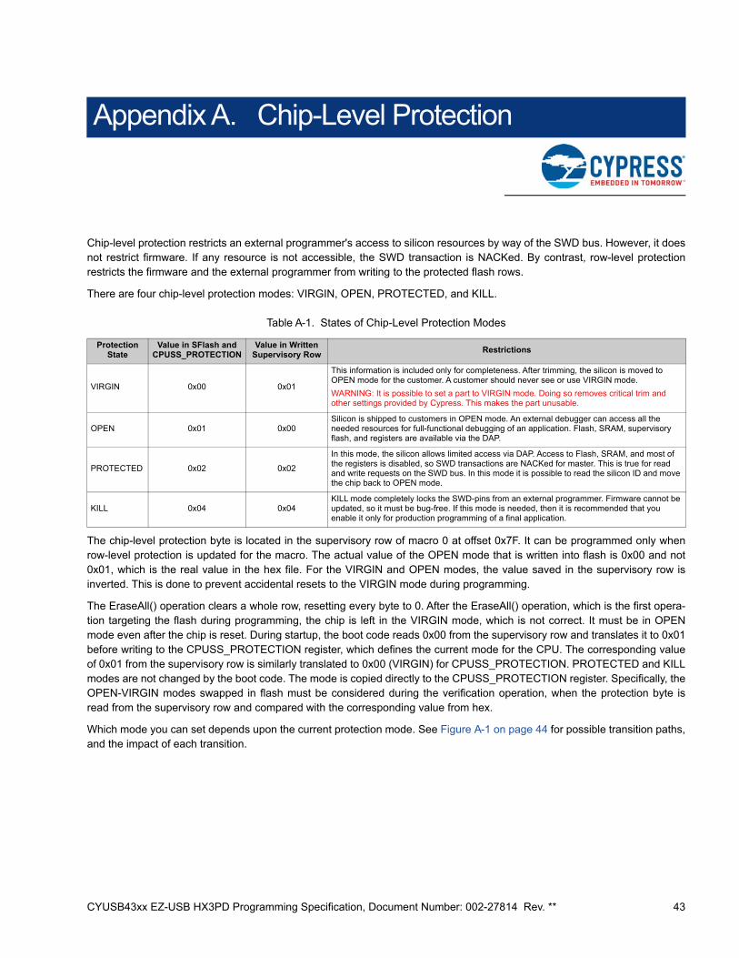
CYUSB43xx EZ-USB HX3PD Programming Specification, Document Number: 002-27814 Rev. ** 43
Appendix A. Chip-Level Protection
Chip-level protection restricts an external programmer's access to silicon resources by way of the SWD bus. However, it doesnot restrict firmware. If any resource is not accessible, the SWD transaction is NACKed. By contrast, row-level protectionrestricts the firmware and the external programmer from writing to the protected flash rows.
There are four chip-level protection modes: VIRGIN, OPEN, PROTECTED, and KILL.
Table A-1. States of Chip-Level Protection Modes
The chip-level protection byte is located in the supervisory row of macro 0 at offset 0x7F. It can be programmed only whenrow-level protection is updated for the macro. The actual value of the OPEN mode that is written into flash is 0x00 and not0x01, which is the real value in the hex file. For the VIRGIN and OPEN modes, the value saved in the supervisory row isinverted. This is done to prevent accidental resets to the VIRGIN mode during programming.
The EraseAll() operation clears a whole row, resetting every byte to 0. After the EraseAll() operation, which is the first opera-tion targeting the flash during programming, the chip is left in the VIRGIN mode, which is not correct. It must be in OPENmode even after the chip is reset. During startup, the boot code reads 0x00 from the supervisory row and translates it to 0x01before writing to the CPUSS_PROTECTION register, which defines the current mode for the CPU. The corresponding valueof 0x01 from the supervisory row is similarly translated to 0x00 (VIRGIN) for CPUSS_PROTECTION. PROTECTED and KILLmodes are not changed by the boot code. The mode is copied directly to the CPUSS_PROTECTION register. Specifically, theOPEN-VIRGIN modes swapped in flash must be considered during the verification operation, when the protection byte isread from the supervisory row and compared with the corresponding value from hex.
Which mode you can set depends upon the current protection mode. See Figure A-1 on page 44 for possible transition paths,and the impact of each transition.
Protection State
Value in SFlash and CPUSS_PROTECTION
Value in Written Supervisory Row
Restrictions
VIRGIN 0x00 0x01
This information is included only for completeness. After trimming, the silicon is moved to OPEN mode for the customer. A customer should never see or use VIRGIN mode.
WARNING: It is possible to set a part to VIRGIN mode. Doing so removes critical trim and other settings provided by Cypress. This makes the part unusable.
OPEN 0x01 0x00Silicon is shipped to customers in OPEN mode. An external debugger can access all the needed resources for full-functional debugging of an application. Flash, SRAM, supervisory flash, and registers are available via the DAP.
PROTECTED 0x02 0x02
In this mode, the silicon allows limited access via DAP. Access to Flash, SRAM, and most of the registers is disabled, so SWD transactions are NACKed for master. This is true for read and write requests on the SWD bus. In this mode it is possible to read the silicon ID and move the chip back to OPEN mode.
KILL 0x04 0x04KILL mode completely locks the SWD-pins from an external programmer. Firmware cannot be updated, so it must be bug-free. If this mode is needed, then it is recommended that you enable it only for production programming of a final application.
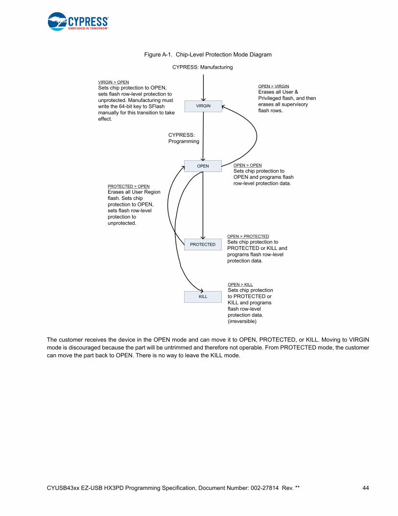
CYUSB43xx EZ-USB HX3PD Programming Specification, Document Number: 002-27814 Rev. ** 44
Figure A-1. Chip-Level Protection Mode Diagram
The customer receives the device in the OPEN mode and can move it to OPEN, PROTECTED, or KILL. Moving to VIRGINmode is discouraged because the part will be untrimmed and therefore not operable. From PROTECTED mode, the customercan move the part back to OPEN. There is no way to leave the KILL mode.
VIRGIN
OPEN > KILL
Sets chip protection to PROTECTED or KILL and programs flash row-level protection data. (irreversible)
PROTECTED > OPEN
Erases all User Region flash. Sets chip protection to OPEN, sets flash row-level protection to unprotected.
OPEN
PROTECTED
KILL
OPEN > VIRGIN
Erases all User & Privileged flash, and then erases all supervisory flash rows.
OPEN > PROTECTED
Sets chip protection to PROTECTED or KILL and programs flash row-level protection data.
VIRGIN > OPEN
Sets chip protection to OPEN, sets flash row-level protection to unprotected. Manufacturing must write the 64-bit key to SFlash manually for this transition to take effect.
CYPRESS: Manufacturing
OPEN > OPEN
Sets chip protection to OPEN and programs flash row-level protection data.
CYPRESS: Programming
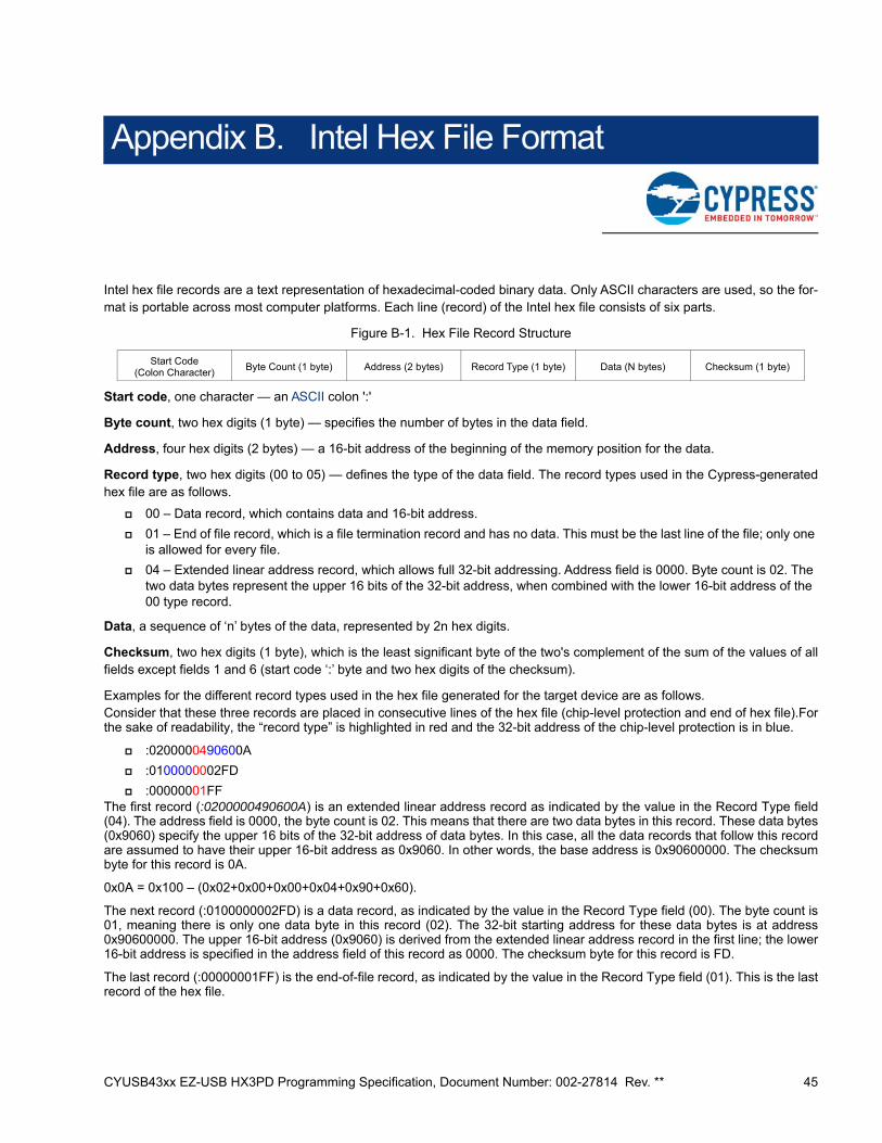
CYUSB43xx EZ-USB HX3PD Programming Specification, Document Number: 002-27814 Rev. ** 45
Appendix B. Intel Hex File Format
Intel hex file records are a text representation of hexadecimal-coded binary data. Only ASCII characters are used, so the for-mat is portable across most computer platforms. Each line (record) of the Intel hex file consists of six parts.
Figure B-1. Hex File Record Structure
Start code, one character — an ASCII colon ':'
Byte count, two hex digits (1 byte) — specifies the number of bytes in the data field.
Address, four hex digits (2 bytes) — a 16-bit address of the beginning of the memory position for the data.
Record type, two hex digits (00 to 05) — defines the type of the data field. The record types used in the Cypress-generatedhex file are as follows.
00 – Data record, which contains data and 16-bit address.
01 – End of file record, which is a file termination record and has no data. This must be the last line of the file; only one is allowed for every file.
04 – Extended linear address record, which allows full 32-bit addressing. Address field is 0000. Byte count is 02. The two data bytes represent the upper 16 bits of the 32-bit address, when combined with the lower 16-bit address of the 00 type record.
Data, a sequence of ‘n’ bytes of the data, represented by 2n hex digits.
Checksum, two hex digits (1 byte), which is the least significant byte of the two's complement of the sum of the values of allfields except fields 1 and 6 (start code ‘:’ byte and two hex digits of the checksum).
Examples for the different record types used in the hex file generated for the target device are as follows.Consider that these three records are placed in consecutive lines of the hex file (chip-level protection and end of hex file).Forthe sake of readability, the “record type” is highlighted in red and the 32-bit address of the chip-level protection is in blue.
:0200000490600A
:0100000002FD
:00000001FFThe first record (:0200000490600A) is an extended linear address record as indicated by the value in the Record Type field(04). The address field is 0000, the byte count is 02. This means that there are two data bytes in this record. These data bytes(0x9060) specify the upper 16 bits of the 32-bit address of data bytes. In this case, all the data records that follow this recordare assumed to have their upper 16-bit address as 0x9060. In other words, the base address is 0x90600000. The checksumbyte for this record is 0A.
0x0A = 0x100 – (0x02+0x00+0x00+0x04+0x90+0x60).
The next record (:0100000002FD) is a data record, as indicated by the value in the Record Type field (00). The byte count is01, meaning there is only one data byte in this record (02). The 32-bit starting address for these data bytes is at address0x90600000. The upper 16-bit address (0x9060) is derived from the extended linear address record in the first line; the lower16-bit address is specified in the address field of this record as 0000. The checksum byte for this record is FD.
The last record (:00000001FF) is the end-of-file record, as indicated by the value in the Record Type field (01). This is the lastrecord of the hex file.
Start Code (Colon Character)
Byte Count (1 byte) Address (2 bytes) Record Type (1 byte) Data (N bytes) Checksum (1 byte)
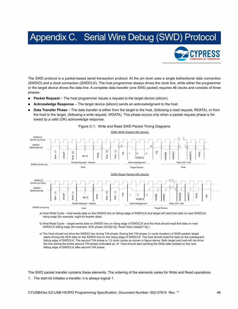
CYUSB43xx EZ-USB HX3PD Programming Specification, Document Number: 002-27814 Rev. ** 46
Appendix C. Serial Wire Debug (SWD) Protocol
The SWD protocol is a packet-based serial transaction protocol. At the pin level uses a single bidirectional data connection(SWDIO) and a clock connection (SWDCLK). The host programmer always drives the clock line, while either the programmeror the target device drives the data line. A complete data transfer (one SWD packet) requires 46 clocks and consists of threephases:
Packet Request – The host programmer issues a request to the target device (silicon).
Acknowledge Response – The target device (silicon) sends an acknowledgment to the host.
Data Transfer Phase – The data transfer is either from the target to the host, (following a read request, RDATA), or from the host to the target, (following a write request, WDATA). This phase occurs only when a packet request phase is fol-lowed by a valid (OK) acknowledge response.
Figure C-1. Write and Read SWD Packet Timing Diagrams
The SWD packet transfer contains these elements. The ordering of the elements varies for Write and Read operations.
1. The start bit initiates a transfer; it is always logical 1.
Sta
rt
(1
)
AP
nDP
Rn
W
(0)
A[2:3]
Par
ity
Sto
p
(0)
Par
k
(1)
TrN 1 0 0
ACK[0:2]
wda
ta[0
]
wd
ata[
1]
wda
ta[3
1]
Par
ity
SWDIO driven by:Host Target Device Host
SWDCLK(Driven by Host)
SWDIO(Bidirectional)
TrN
zz
SWD Write Packet (46 clocks)
SWD Read Packet (46 clocks)
Sta
rt (
1)
AP
nD
P
Rn
W (
1)
A[2:3] Par
ity
Sto
p
(0)
Par
k(1
)
TrN 1 0 0
ACK[0:2] rdat
a[0]
rdat
a[1]
rdat
a[3
0]
rda
ta[3
1]
Par
ity
TrN
SWDIO driven by: Host Target Device
SWDCLK(Driven by Host)
SWDIO(Bidirectional)
a) Host Write Cycle – host sends data on the SWDIO line on falling edge of SWDCLK and target will read that data on next SWDCLK rising edge (for example, eight bit header data).
b) Host Read Cycle – target sends data on SWDIO line on rising edge of SWDCLK and the Host should read that data on next SWDCLK falling edge (for example, ACK phase (ACK[2:0]), Read Data (rdata[31:0]) ).
c) The Host should not drive the SWDIO line during TrN phase. During first TrN phase (½ cycle duration) of SWD packet, target starts driving the ACK data on the SWDIO line on the rising edge of SWDCLK. The host should read the data on the subsequent falling edge of SWDCLK. The second TrN phase is 1.5 clock cycles as shown in figure above. Both target and host will not drive the line during the entire second TrN phase (indicated as zᶲ Host should start sending the Write data (wdata) on the next falling edge of SWDCLK after second TrN phase.
Packet Request - Header Acknowledgement Data (32+1 bit)
Packet Request - Header Acknowledgement Data (32+1 bit)
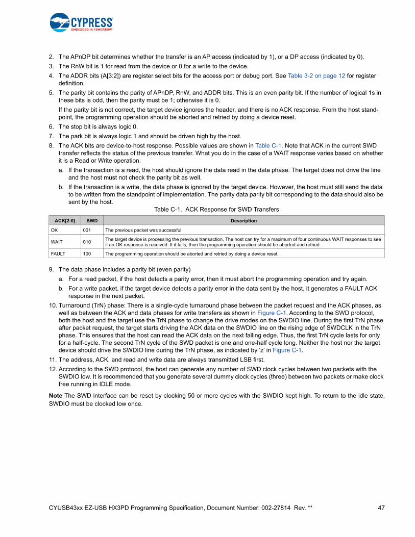
CYUSB43xx EZ-USB HX3PD Programming Specification, Document Number: 002-27814 Rev. ** 47
2. The APnDP bit determines whether the transfer is an AP access (indicated by 1), or a DP access (indicated by 0).
3. The RnW bit is 1 for read from the device or 0 for a write to the device.
4. The ADDR bits (A[3:2]) are register select bits for the access port or debug port. See Table 3-2 on page 12 for register definition.
5. The parity bit contains the parity of APnDP, RnW, and ADDR bits. This is an even parity bit. If the number of logical 1s in these bits is odd, then the parity must be 1; otherwise it is 0.
If the parity bit is not correct, the target device ignores the header, and there is no ACK response. From the host stand-point, the programming operation should be aborted and retried by doing a device reset.
6. The stop bit is always logic 0.
7. The park bit is always logic 1 and should be driven high by the host.
8. The ACK bits are device-to-host response. Possible values are shown in Table C-1. Note that ACK in the current SWD transfer reflects the status of the previous transfer. What you do in the case of a WAIT response varies based on whether it is a Read or Write operation.
a. If the transaction is a read, the host should ignore the data read in the data phase. The target does not drive the line and the host must not check the parity bit as well.
b. If the transaction is a write, the data phase is ignored by the target device. However, the host must still send the data to be written from the standpoint of implementation. The parity data parity bit corresponding to the data should also be sent by the host.
9. The data phase includes a parity bit (even parity)
a. For a read packet, if the host detects a parity error, then it must abort the programming operation and try again.
b. For a write packet, if the target device detects a parity error in the data sent by the host, it generates a FAULT ACK response in the next packet.
10. Turnaround (TrN) phase: There is a single-cycle turnaround phase between the packet request and the ACK phases, as well as between the ACK and data phases for write transfers as shown in Figure C-1. According to the SWD protocol, both the host and the target use the TrN phase to change the drive modes on the SWDIO line. During the first TrN phase after packet request, the target starts driving the ACK data on the SWDIO line on the rising edge of SWDCLK in the TrN phase. This ensures that the host can read the ACK data on the next falling edge. Thus, the first TrN cycle lasts for only for a half-cycle. The second TrN cycle of the SWD packet is one and one-half cycle long. Neither the host nor the target device should drive the SWDIO line during the TrN phase, as indicated by ‘z’ in Figure C-1.
11. The address, ACK, and read and write data are always transmitted LSB first.
12. According to the SWD protocol, the host can generate any number of SWD clock cycles between two packets with the SWDIO low. It is recommended that you generate several dummy clock cycles (three) between two packets or make clock free running in IDLE mode.
Note The SWD interface can be reset by clocking 50 or more cycles with the SWDIO kept high. To return to the idle state,SWDIO must be clocked low once.
Table C-1. ACK Response for SWD Transfers
ACK[2:0] SWD Description
OK 001 The previous packet was successful.
WAIT 010The target device is processing the previous transaction. The host can try for a maximum of four continuous WAIT responses to see if an OK response is received. If it fails, then the programming operation should be aborted and retried.
FAULT 100 The programming operation should be aborted and retried by doing a device reset.
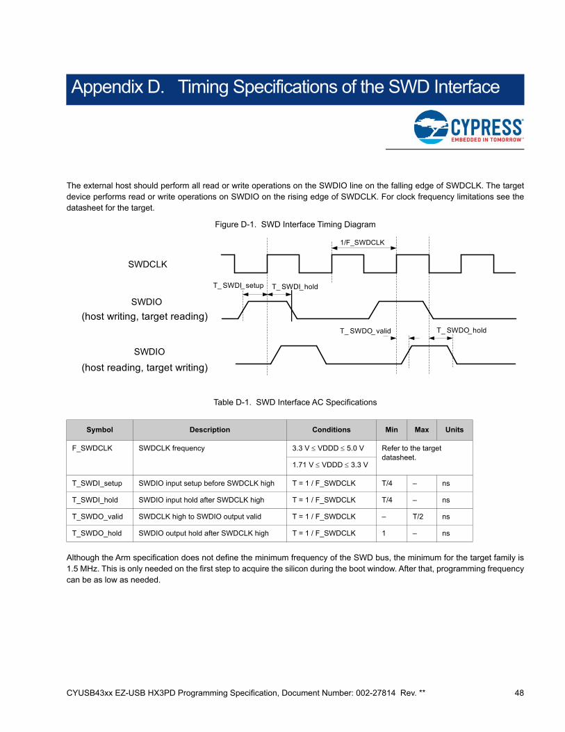
CYUSB43xx EZ-USB HX3PD Programming Specification, Document Number: 002-27814 Rev. ** 48
Appendix D. Timing Specifications of the SWD Interface
The external host should perform all read or write operations on the SWDIO line on the falling edge of SWDCLK. The targetdevice performs read or write operations on SWDIO on the rising edge of SWDCLK. For clock frequency limitations see thedatasheet for the target.
Figure D-1. SWD Interface Timing Diagram
Table D-1. SWD Interface AC Specifications
Although the Arm specification does not define the minimum frequency of the SWD bus, the minimum for the target family is1.5 MHz. This is only needed on the first step to acquire the silicon during the boot window. After that, programming frequencycan be as low as needed.
Symbol Description Conditions Min Max Units
F_SWDCLK SWDCLK frequency 3.3 V VDDD 5.0 V Refer to the target datasheet.
1.71 V VDDD 3.3 V
T_SWDI_setup SWDIO input setup before SWDCLK high T = 1 / F_SWDCLK T/4 – ns
T_SWDI_hold SWDIO input hold after SWDCLK high T = 1 / F_SWDCLK T/4 – ns
T_SWDO_valid SWDCLK high to SWDIO output valid T = 1 / F_SWDCLK – T/2 ns
T_SWDO_hold SWDIO output hold after SWDCLK high T = 1 / F_SWDCLK 1 – ns
SWDIO
SWDCLK
SWDIO
(host writing, target reading)
(host reading, target writing)
T_ SWDI_ setup T_ SWDI_hold
T_ SWDO_ valid T_ SWDO_hold
1/F_SWDCLK
CYUSB43xx EZ-USB HX3PD Programming Specification, Document Number: 002-27814 Rev. ** 49
Revision History
Document Title: CYUSB43xx EZ-USB HX3PD Programming Specification
Document Number: 002-27814
Revision ECN# Issue Date Description of Change
** 6616066 07/08/2019 New specification.
Related Documents


