This article appeared in a journal published by Elsevier. The attached copy is furnished to the author for internal non-commercial research and education use, including for instruction at the authors institution and sharing with colleagues. Other uses, including reproduction and distribution, or selling or licensing copies, or posting to personal, institutional or third party websites are prohibited. In most cases authors are permitted to post their version of the article (e.g. in Word or Tex form) to their personal website or institutional repository. Authors requiring further information regarding Elsevier’s archiving and manuscript policies are encouraged to visit: http://www.elsevier.com/copyright

Welcome message from author
This document is posted to help you gain knowledge. Please leave a comment to let me know what you think about it! Share it to your friends and learn new things together.
Transcript
This article appeared in a journal published by Elsevier. The attachedcopy is furnished to the author for internal non-commercial researchand education use, including for instruction at the authors institution
and sharing with colleagues.
Other uses, including reproduction and distribution, or selling orlicensing copies, or posting to personal, institutional or third party
websites are prohibited.
In most cases authors are permitted to post their version of thearticle (e.g. in Word or Tex form) to their personal website orinstitutional repository. Authors requiring further information
regarding Elsevier’s archiving and manuscript policies areencouraged to visit:
http://www.elsevier.com/copyright
Author's personal copy
Cyclic endurance reliability of stretchable electronic substrates
F. Bossuyt a, J. Guenther b, T. Löher c, M. Seckel c, T. Sterken a, J. de Vries d,⇑a IMEC/University Ghent, Technologiepark 914A, 9052 Zwijnaarde, Belgiumb Freudenberg Forschungsdienste KG, Hoehnerweg 2–4, 69469 Weinheim, Germanyc Technische Universität Berlin, Gustav-Meyer-Allee 25, D-13355 Berlin, Germanyd Philips Applied Technologies, High Tech Campus 7, 5656 AE Eindhoven, The Netherlands
a r t i c l e i n f o
Article history:Received 1 June 2010Received in revised form 23 September 2010Accepted 23 September 2010Available online 16 October 2010
a b s t r a c t
Stretchable electronic circuit boards have been developed based on three different technologies. Suchsubstrates serve to connect rigid interposers or electronic components. The conducting traces have ameandering shape and consist of Cu-foil or screen-printed Ag-paste. These conducting traces are attachedto or embedded in polyurethane, polydimethylsiloxane, or breathable non-woven stretchable substratematerial. The long-term endurance behavior of this novel type of boards is studied by cyclic elongationat strain ranges of up to 20% and monitoring the electrical connectivity. The main failure mode in theCu-foil based technologies is fatigue of the conducting traces and can be described in terms of the Man-son–Coffin relation. Indications for high-cycle fatigue were found. The screen-printed conductors on non-woven substrates fail by breaking of the connection between the metallic grains. The application areasare electronic monitoring systems that need to be placed directly on the skin, or conformable systemsfor curved surfaces.
� 2010 Elsevier Ltd. All rights reserved.
1. Introduction
In the past consumer electronics were discrete, heavy weightand usually indoor products. Later technological developments en-abled the introduction of ever more electronic applications, whichamongst others led to the abundant availability of portable elec-tronic products. Today one can observe, amongst many trends,the development of wearable electronics.
There is a growing need, or at least a desire, to monitor humanbody functions during longer periods of time, not only while visit-ing a physician or therapist. This asks for sensors that can be placedclose to or even on the skin. This proximity is required in order todetect weak signals. At the same time such sensors and the elec-tronic circuits to which these are connected should not hamperthe comfort of the user. Preferably the application should feel liketextile. This excludes the use of rigid but also of flexible substratesas printed circuit boards, because once bent flexible materials arevery stiff in the direction perpendicular to the bending axis.
One solution is to attach the electronic circuit onto the textile forwhich, ideally, all parts must be stretchable. Electronic componentsare not stretchable. However, stretchability of the whole system canbe realized by a stretchable circuit board, electrically connecting thedifferent, rigid surface mount components. Three such stretchablecircuit board technologies will be discussed in this study.
The obvious question then concerns the reliability of suchstretchable electronics, more specifically the long-term perfor-mance of their stretchability and connectivity. Wearability willundoubtedly involve – depending on the application – large num-bers of stretching cycles of a few percent to a smaller number ofabout 10%. To illustrate this one can think of a sensor monitoringone’s heartbeat which is placed several times per day on an armor leg stretching up to 10% and then used while doing exercisesrequiring up to 3% stretch for many thousand cycles. Should suchsensor require a lifetime of a year or more, one needs in the orderof 104 cycles of 5–10% stretch and around 106 cycles of 1–3%. Therelation to translate between different test conditions is the mainitem. This allows extrapolation to operational load cases. Closelyconnected to the subject are the requirements for the aforemen-tioned applications. Although the requirements are of importance,these will not be addressed further in this study.
In this paper first a summary overview of stretchable electron-ics will be given, including a brief account of the reliability assess-ment. Next, the technologies for stretchable electronic substrateswill be introduced together with the test structures and test proce-dures. The measurement results and failure analyses are topic ofthe third section. In the discussion the failure mechanism will beaddressed and brief attention paid to extrapolate the results touse conditions. This paper focuses on the stretchability and con-nectivity of the electrical conductors at cyclic mechanical loading.Degradation and aging of the stretchable substrate materials itselfis beyond the scope of this report.
0026-2714/$ - see front matter � 2010 Elsevier Ltd. All rights reserved.doi:10.1016/j.microrel.2010.09.032
⇑ Corresponding author.E-mail address: [email protected] (J. de Vries).
Microelectronics Reliability 51 (2011) 628–635
Contents lists available at ScienceDirect
Microelectronics Reliability
journal homepage: www.elsevier .com/locate /microrel
Author's personal copy
The technologies that will be dealt with in this paper have beentreated in detail elsewhere [1–3]. Here only a brief description willbe given for better understanding.
2. Stretchable technology
Different approaches are found in literature to realize elastic,stretchable electronic devices and systems. To make intrinsic,non-stretchable materials (e.g. silicon, metal conductors) stretch-able, in-plane or out-of-plane designs are used to accommodatethe applied strains. Those materials are used in combination withan elastomer, e.g. polydimethylsiloxane (PDMS) acting as a carrieror encapsulant [4–7].
In one out-of-plane design approach, structures of inorganicsbonded to or embedded in elastomeric substrates (PDMS) givereversible responses to large strain deformations [8]. For example,wavy silicon structures can accommodate strain ranges of 15–20%before fracture. Out-of-plane inorganic systems where the wavysilicon is selectively bonded to the PDMS substrate can withstandmuch larger strains.
Another out-of-plane approach is used to produce stretchablethin gold metal films on a PDMS substrate [9,10]. The substrateis pre-stretched while metals are deposited by vapour phase depo-sition. Micro-cracking occurs in addition to the wavy structuresand both phenomena contribute to the stretchable mechanical re-sponse. Interconnects prepared with 25% pre-strain could bestretched by 100% with only slight increase of the electrical resis-tance, which proves that not only the wavy structures determinethe behavior. In [11], gold thin-film conductors on elastomeric sub-strates were subjected to extensive cyclic loading, up to 250,000cycles to 20% strain. They presented stable electrical conductionover cycling. It was shown that after 1000 stretch cycles, the initialmicrocrack pattern built in the gold film evolved into a stable is-land-like array, which guaranteed electrical continuity even after250,000 cycles. The samples were still conducting, but the resistiv-ity had increased by several orders of magnitude.
A third approach was presented by [12]. Embedded conductorswere developed based on conductive adhesives containing Ag fillerparticles dispersed in a silicone binder on a silicone substrate.These printed conductors were subjected to tensile testing up to100–150% showing an increase of the resistance but no completefailure. After removing the strain a recovery of the resistance wasfound. However, no explicit cyclic loading has been reported onthis technology.
Whereas for metal conductors almost exclusively out-of-planetechnologies have been developed, in this study technologies tomake in-plane stretchable electronics will be treated.
3. Test samples
Polydimethylsiloxane (PDMS) and polyurethane (PU) have verygood elastic properties and allow for different approaches in pro-cess technologies. The non-woven materials have the great advan-tage of being permeable to liquids and gases (in the followingreferred to as breathable). These are the essential reasons to choosethese materials for the stretchable substrate technologies.
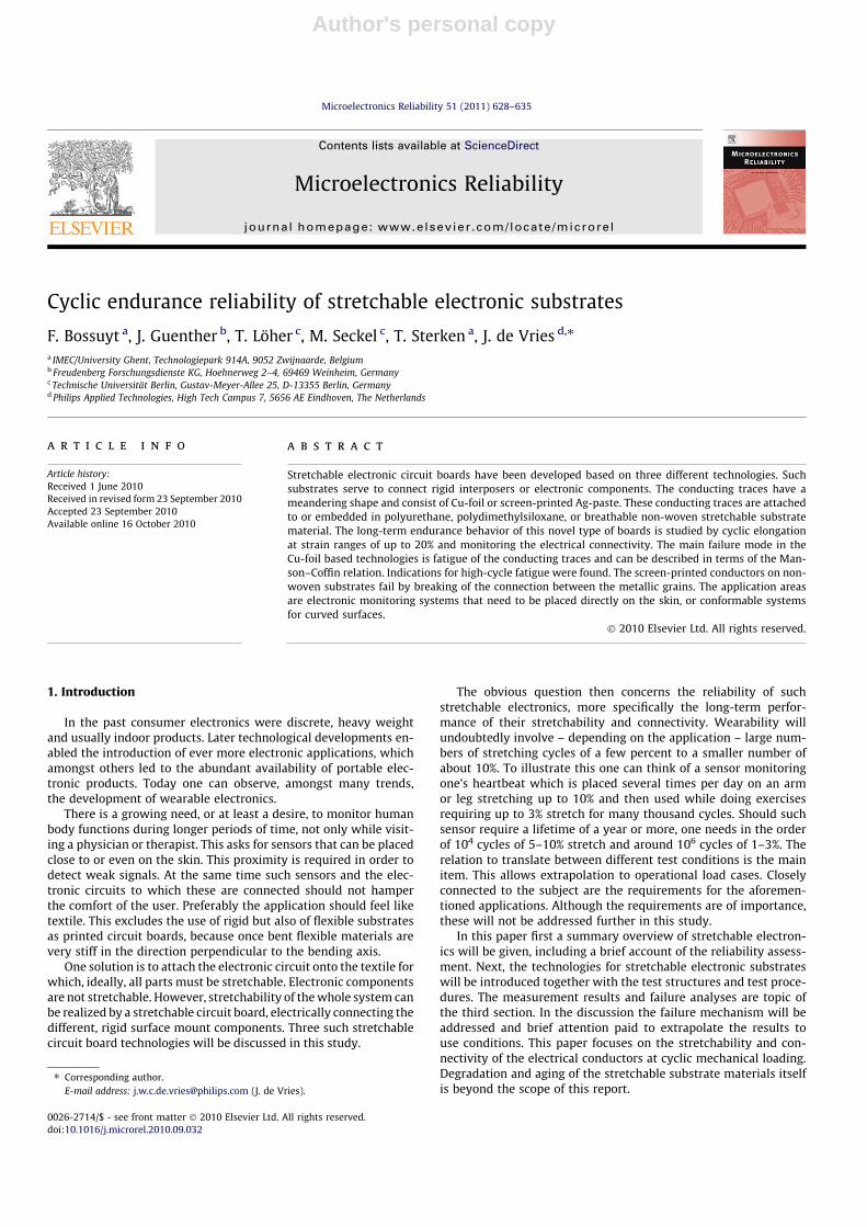
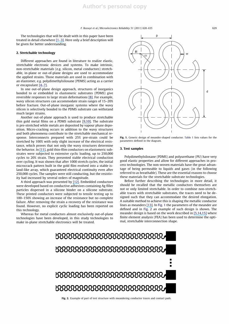
Before further describing the technologies in more detail, itshould be recalled that the metallic conductors themselves arenot or only limited stretchable. In order to combine non-stretch-able traces with stretchable substrates, the traces need to be de-signed such that they can accommodate the desired elongation.A suitable method to achieve this is shaping the metallic conductorlines as meanders [13]. In Fig. 1 the parameters of the meander aredefined and in Fig. 2 an example of such design is shown. Themeander design is based on the work described in [5,14,15] wherefinite element analysis (FEA) has been used to determine the opti-mal, stretchable interconnection shape.
Fig. 1. Generic design of meander-shaped conductor. Table 1 lists values for theparameters defined in the diagram.
Fig. 2. Example of part of test structure with meandering conductor traces and contact pads.
F. Bossuyt et al. / Microelectronics Reliability 51 (2011) 628–635 629

Author's personal copy
The optimum in simulation for stretchable copper board (SCB)and stretchable molded interconnection (SMI) is only valid for bulkPU/silicone, no simulations on non-woven material that is used forstretchable polymer board (SPB) have been done. The non-wovensubstrate does not allow printed structures below 1 mm size.Therefore as a compromise between straight lines, with smallstretchability, and large resistance because of extra length, the spe-cific resistance of conductive paste is two decades higher than forbare Cu, half circles were designed and the number of meanderswas adjusted to obtain good conductivity (see Table 1). See alsothe paragraph on SPB-technology in this section.
Components are grouped on functional islands and connectedto each other with stretchable copper tracks both embedded in astretchable material.
3.1. Stretchable copper board
The stretchable copper board technology (SCB, [2]) is very sim-ilar to the fabrication of a single sided rigid or flexible printed cir-cuit board. The main difference to conventional printed circuittechnology is the organic substrate material, which is polyurethane(PU) instead of polyimide (flex) or epoxy (rigid).
The SCB-samples used for cyclic stretch loading consist ofmeandering Cu traces terminated at both ends by large contactpads. They are designed for continuity measurements. The sampleshave a total thickness of 80 lm.
The Cu trace thickness is 35 lm, which is made by patterning ofcommercially available Cu-foil as used in printed circuit boardmanufacturing. The width of the Cu traces is 100 lm. The mean-ders had a wavelength of 2 mm and amplitude of 1.1 mm. Afterpatterning of the copper, the whole surface is laminated by a coverlayer of polyurethane with a thickness of 50 lm.
3.2. Stretchable molded interconnection
In stretchable molded interconnection technology (SMI, [3]) acopper foil is laminated by use of a temporary adhesive (wax) ona rigid/flexible carrier (FR4-substrate). By standard PCB-tech-niques, an electronic circuit is produced by lithographical pattern-ing and wet-etching of the copper, application of soldermask,copper finish (OSP) and mounting electronic components by reflowsoldering. One difference with a normal PCB-board is the copperbeing held by the temporary adhesive on the board. This electronicsystem is molded in a stretchable material by covering the top partby injection molding of PDMS, removing the temporary carrier by
heating up the wax and injection molding the back part. In thisway, a stretchable electronic system is obtained.
For this study, SMI-technology samples were made by use of18 lm TW–YE copper foil (Circuitfoil) and Sylgard 186 (Dow Corn-ing) as embedding material. The sample consists of parallel mean-der (horseshoe) tracks connected with a flexible interconnection tothe outside. The amount of meanders per track and the character-istics of the meanders are summarized in Table 1. A dedicatedmold was used to have a smooth, stress releasing transition be-tween the different thicknesses of the Sylgard 186 on top of themeanders and at the connection pad.
3.3. Stretchable polymer board
Stretchable polymer board (SPB, [1]) uses classical screen print-ing to structure the circuit by applying a printable and conductivepaste onto a stretchable base material (Evolon� Polyurethanemicro fiber non-woven). Since the goal was to develop a stretch-able product both the conductor and the base material neededstretchability as intrinsic properties. As discussed before stretch-ability can be achieved using geometrical designs that allow evenfor non-stretchable materials like Cu a significant stretching. ForSPB a specific paste has been developed that allows also a primarystretching of the printed conductors. For this purpose thermoplas-tic polyurethane has been used as polymer matrix. Ag-coatedflakes have been selected as conducting particles and a waterbased paste has been developed that allows a variation of thefraction of the conductive filler and by thus a variety of pastes interms of the resistance per square. However, since a systematicvariation was not the focus of this study of reliability aspects therecipe had been fixed.
After printing the conductive layer a drying and thermosettingprocess is performed. This is different from classical screen print-ing where a curing process is the only process step to finalize theflexible printed boards. The overall dimensions of the test samplesof SPB-technology are 260 mm length and a width of 50 mm (seeFig. 3). The typical layer thickness after printing, drying and press-ing is 100–150 lm.
4. Experimental
Before the actual endurance tests were carried out, the maxi-mum elongation that can be achieved with the various technolo-gies was determined. This was done by stretching the samples ina test machine at a strain rate of 1%/s and continuously monitoring
Table 1Characteristics of stretchable test samples. The geometrical parameters are defined inFig. 1. XO-90: polyurethane non-woven.
Item Unit SMI SCB SPB
Total length of sample mm 50 250 262Total width of sample mm 18 40 50Effective length for cyclic
stretchingmm 46 100 230
# Parallel stretchable tracksper sample
– 22 6 2
Parallel stretchable trackpitch (d)
mm 3 3 n/a
# Meanders per track – 50 50 6Meander track width (w) mm 0.1 0.1 3Meander angle (h) � 45 41 0Meander radius (R) mm 0.35 0.66 9Meander period (p) mm 0.99 2.0 36Embedding/support material – Sylgard
186�Walopur4201�
XO-90�
Embedding/support materialthickness
– 1 mm 130 lm 90 g/m2
Fig. 3. Layout of SPB-test structure. The total length and width are 250 � 40 mm.Details are listed in Table 1.
Table 2Settings used in endurance tests.
SCB SMI SPB
Current applied per track(mA)
1 12.5 1
Cyclic strain rate (%/s) 1 1 1Failure criterion Open Open n.a., see textSampling frequency At maximum
stretch0.4 Hz 3 Hz
630 F. Bossuyt et al. / Microelectronics Reliability 51 (2011) 628–635
Author's personal copy
their electrical connectivity. For the subsequent cyclic stretch tests,the strain range was chosen to be well below this maximum elon-gation. In the remainder of this study, whenever ‘strain’ is men-tioned, the authors mean the so-called engineering strain. This isthe relative change of length calculated from the dimensionalchanges of the sample, and explicitly not taking into account localstrain concentrations and variations. In Table 2 the most relevantexperimental settings are listed.
For SCB each test sample has a total length of 25 cm and a widthof 4 cm. The connector pads to attach the continuity prober areoutside the part of the sample that is stretched during the experi-ment. A small stripe of FR4 rigid printed circuit board is attachedon the backside of the substrates at the contact pads, in order to
ease the contacting of wires to the measure equipment. In fact onlya section of 10 cm in the middle of the sample is stretched duringthe experiment. At these positions the sample is clamped into thetest equipment. The clamps consist of a flat anvil on one side and a
Table 3Maximum elongation (e), force (F) and stress (r) at failure for stretchable substratetechnology.
Technology e (%) F (N) r (MPa)
SCB 45 ± 6 21 ± 3 0.50 ± 0.07SMI 60 ± 3 10 ± 1 0.24 ± 0.02SPB 9 ± 2 14 ± 3 1.7 ± 0.3
0
2
4
6
8
10
0 200 400 600 800 1000 1200cycles
R (Ω
)
Fig. 4. Example of endurance test on SCB-samples 0–7.5%.
0
10
20
30
40
50
0 1000 2000 3000 4000
R (Ω
)
cycles
Fig. 5. Example of endurance test on SMI-samples 0–7.5%.
cycles to failure
Cum
ulat
ive
failu
res
(%)
100 1000001000 100001
5
10
50
90
99
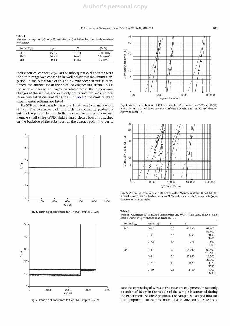
Fig. 6. Weibull-distributions of SCB-test samples. Maximum strain 2.5% (N), 5% (s),and 7.5% (d). Dashed lines are 90%-confidence levels. The symbol (I) denotessurviving samples.
cycles to failure
Cum
ulat
ive
failu
res
(%)
100 10000001000 10000 1000001
5
10
50
90
99
Fig. 7. Weibull-distributions of SMI-test samples. Maximum strain 4% (N), 5% (s),7.5% (j), and 10% (e). Dashed lines are 90%-confidence levels. The symbols (I, .)denote surviving samples.
Table 4Weibull parameters for indicated technologies and cyclic strain tests. Shape (b) andscale parameter (g, with 90%-confidence levels).
Technology Strain (%) b g
SCB 0–2.5 7.3 47,800 42,60053,600
0–5 11.3 3250 30503460
0–7.5 6.4 975 8601100
SMI 0–4 7.1 105,000 92,400119,500
0–5 3.1 17,900 13,50023,700
0–7.5 10.1 3420 31203730
0–10 2.8 2420 17003430
F. Bossuyt et al. / Microelectronics Reliability 51 (2011) 628–635 631
Author's personal copy
smoothly rounded wedge on the other. Both anvil and wedge arecoated with polyurethane to provide a firm grip of the clamp andto prevent damage to the sample.
The test apparatus was a home-build machine using an electri-cally driven step motor with a maximum displacement of 40 cm.Travelling speed and acceleration can be numerically controlledand were set such, that the elongation rate was equal to 1%/s. Con-tinuity data acquisition (two-point measurement) was done usinga Keithley 2750. Continuity was measured only when the sampleswere fully elongated, after which the measured resistances werecollected and stored. The end of life was defined as the momentwhere the conductivity goes to zero.
For SMI each test sample has a total length of 5 cm and a widthof 1.8 cm. A dedicated clamping tool was made in order to clampthe sample without having too much orthogonal force on thecontact pads. The actual stretchable length of the sample is4.6 cm, because the sample is clamped at the contact pads. Forthe SMI-technology sample testing, an Instron 5543 has been usedfor performing the cyclic stretch tests. The measurement was doneby use of a four-point resistance measurement system. The end oflife was defined as the point where the conductivity goes to zero.
For SPB-technology a home-build linear test bench was usedincluding an electrically driven linear step motor and a four-pointresistance measurement system based on a Prema 6001. Thesamples were fixed by two gold plated contact bars at each sideof the sample. These bars served as mechanical clamping as wellas for the electrical contacts.
The measured data (length and resistance) were recorded at3 Hz with a LabView I/O-card with 16 bit resolution. The LabViewprogram ran also the linear test bench at the corresponding speed(1%/s). Since the change in resistance is less abrupt in polymer con-ductors no a priori lifetime criterion was defined to stop the test.The definition of end of life was a posteriori implemented intothe data analysis.
The results were analyzed with Reliasoft Weibull++ software(version 7). Visual inspection of the surfaces served to identifythe failure mode. To do this, packages were selected that failed atdifferent stages of the failure distribution.
5. Results
5.1. Maximum elongation
In Table 3 the maximal engineering strain (see explanation inSection 4) that the test structures can hold are listed. In order tobetter compare the technologies as the samples are made by useof different materials and dimensions, also the stress at failurewas estimated. Based on these results, the endurance tests forthe SCB- and SMI-technologies were done at a maximum of 20%strain. For SPB it was limited to 5% because the maximum engi-neering strain was about 10%.
5.2. Endurance tests
Because the SCB- and SMI-technologies show quite a differentbehavior than SPB, they will be treated in separate parts.
A few examples of test results are shown in Figs. 4 and 5. It willbe clear that the moment of failure can be determined accurately.The increased noise after 2500 cycles in Fig. 5 is caused by crosstalk after interruption of one conductor line. The difference inresistance values is due to including the soldered connections onthe pads as well. In Figs. 6 and 7 a selection of the correspondingWeibull-diagrams of the SCB- and SMI-samples are shown. Forthe further analysis the lifetime was defined as the number of cy-cles to 63.2% failures (the characteristic time to failure in Weibullstatistics). The SMI-sample tested for 0–2.5% strain showed no fail-
ures after 950,000 cycles. In the tests to 2.5% (SCB) and 4% (SMI)not all samples failed.
The failure distributions are characterized by the two parame-ters b (shape parameter, the width of the distribution) and g (scaleparameter, cycles to 63% failures). For the cases where a distribu-tion could be analyzed (Figs. 6 and 7), the results are compiled inTable 4.
The scatter in the values of the shape parameter in the statisti-cal analysis is appreciable, which is largely due to the small num-ber of samples. Still, these values are much larger than unity, whichshows that the load level of all the tests is well in the wear-out re-gion.1 In the next step the failure modes will be identified which isnecessary before one can relate the different test results.
0
20
40
60
80
0 100 200 300 400 500
R (Ω
)
cycles
Fig. 8. Example of endurance test on SPB-samples 0–5%. Recordings: 0% (solid line),5% (dashed line).
N cycles
Cum
ulat
ive
failu
res
(%)
10 10000100 10001
5
10
50
90
99
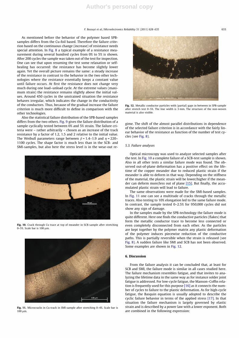
Fig. 9. Weibull-distribution of SPB-test samples. Maximum strain 5%. Failurecriteria: 1.2 (N), 1.5 (s), and 2 (�) times initial resistance.
1 The two-parameter Weibull-function is a probability distribution functiondescribed by a scale parameter (g) denoting its position and a shape parameter (b)denoting its width:
WðtÞ ¼ bg
tg
� �b�1
exp � tg
� �b" #
:
The failure rate decreases over time (t) for b < 1 (early failures), is constant for b = 1(random failures), and increases for b > 1 (aging or wear-out failures).
632 F. Bossuyt et al. / Microelectronics Reliability 51 (2011) 628–635
Author's personal copy
As mentioned before the behavior of the polymer based SPB-samples differs from the Cu-foil based. Therefore the failure crite-rion based on the continuous change (increase) of resistance needsspecial attention. In Fig. 8 a typical example of a resistance mea-surement during several hundred cycles from 0% to 5% is shown.After 200 cycles the sample was taken out of the test for inspection.One can see that upon resuming the test some relaxation or self-healing has occurred: the resistance has become slightly loweragain. Yet the overall picture remains the same: a steady increaseof the resistance in contrast to the behavior in the two other tech-nologies where the resistance essentially keeps a constant valueuntil failure occurs. At first the resistance does not change verymuch during one load–unload cycle. At the extreme values (maxi-mum strain) the resistance remains slightly above the initial val-ues. Around 450 cycles in the unstrained situation the resistancebehaves irregular, which indicates the change in the conductivityof the conductors. Thus, because of the gradual increase the failurecriterion is much more difficult to define in comparison with theother technologies.
Also the statistical failure distribution of the SPB-based samplesdiffers from the two others. Fig. 9 gives the failure distribution of asample cyclically tested between 0% and 5% strain. The failure cri-teria were – rather arbitrarily – chosen as an increase of the trackresistance by a factor of 1.2, 1.5 and 2 relative to the initial value.The Weibull parameters range between b = 1.4–1.9 and g = 220–1100 cycles. The shape factor is much less than in the SCB- andSMI-samples, but also here the stress level is in the wear-out re-
gime. The shift of the almost parallel distributions in dependenceof the selected failure criterion is in accordance with the fairly lin-ear behavior of the resistance as function of the number of test cy-cles (see Fig. 8).
5.3. Failure analyses
Optical microscopy was used to analyze selected samples afterthe test. In Fig. 10 a complete failure of a SCB-test sample is shown.Also in all other tests a similar failure mode was found. The ob-served out-of-plane deformation has a positive effect on the life-time of the copper meander due to reduced plastic strain if themeander is able to deform in that way. Depending on the stiffnessof the material, the plastic strain will be lower/higher if the mean-der can deform more/less out of plane [15]. But finally, the accu-mulated plastic strain will lead to failure.
The same observations were made for the SMI-based samples.In Fig. 11 one can see a multitude of cracks through the metallictraces. Also testing to 10% elongation led to the same failure mode.In contrast, the sample tested 0–2.5% for 950,000 cycles did notshow any sign of damage.
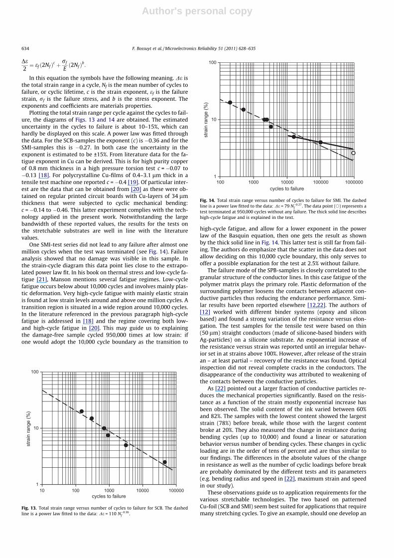
In the samples made by the SPB-technology the failure mode isquite different. Here one finds the conductive particles (flakes) thatform the metallic conductor trace to become less connected oreven completely disconnected from each other. As the particlesare kept together by the polymer matrix any plastic deformationof the polymer induces piecewise reduction of the conductivepaths. This is partially reversible when the strain is released (seeFig. 8). A sudden failure like SMI and SCB has not been observed.Some examples are shown in Fig. 12.
6. Discussion
From the failure analysis it can be concluded that, at least forSCB and SMI, the failure mode is similar in all cases studied here.The failure mechanism resembles fatigue, and that invites to ana-lyzing the lifetime data in the same way as for instance solder jointfatigue is addressed. For low-cycle fatigue, the Manson–Coffin rela-tion is frequently used for this purpose [16] as it connects the num-ber of cycles to failure to the plastic deformation. As for high-cyclefatigue, the Basquin equation is usually adopted to describe thecyclic failure behavior in terms of the applied stress [17]. In thatsituation the failure mechanism is largely governed by elasticstrain and is described by a power law with a lower exponent. Bothare combined in the following expression:
Fig. 10. Crack through Cu trace at top of meander in SCB-sample after stretching0–5%. Scale bar is 100 lm.
Fig. 11. Microcracks in Cu-track in SMI-sample after stretching 0–4%. Scale bar is100 lm.
Fig. 12. Metallic conductor particles with (partial) gaps in between in SPB-sampleafter stretch test 0–5%. The line width is 3 mm. The structure of the non-wovenmaterial is also visible.
F. Bossuyt et al. / Microelectronics Reliability 51 (2011) 628–635 633
Author's personal copy
De2¼ ef ð2Nf Þc þ
rf
Eð2Nf Þb:
In this equation the symbols have the following meaning. De isthe total strain range in a cycle, Nf is the mean number of cycles tofailure, or cyclic lifetime, c is the strain exponent, ef is the failurestrain, rf is the failure stress, and b is the stress exponent. Theexponents and coefficients are materials properties.
Plotting the total strain range per cycle against the cycles to fail-ure, the diagrams of Figs. 13 and 14 are obtained. The estimateduncertainty in the cycles to failure is about 10–15%, which canhardly be displayed on this scale. A power law was fitted throughthe data. For the SCB-samples the exponent (c) is �0.36 and for theSMI-samples this is �0.27. In both case the uncertainty in theexponent is estimated to be ±15%. From literature data for the fa-tigue exponent in Cu can be derived. This is for high purity copperof 0.8 mm thickness in a high pressure torsion test c = �0.07 to�0.13 [18]. For polycrystalline Cu-films of 0.4–3.1 lm thick in atensile test machine one reported c = �0.4 [19]. Of particular inter-est are the data that can be obtained from [20] as these were ob-tained on regular printed circuit boards with Cu-layers of 34 lmthickness that were subjected to cyclic mechanical bending:c = �0.14 to �0.46. This latter experiment complies with the tech-nology applied in the present work. Notwithstanding the largebandwidth of these reported values, the results for the tests onthe stretchable substrates are well in line with the literaturevalues.
One SMI-test series did not lead to any failure after almost onemillion cycles when the test was terminated (see Fig. 14). Failureanalysis showed that no damage was visible in this sample. Inthe strain-cycle diagram this data point lies close to the extrapo-lated power law fit. In his book on thermal stress and low-cycle fa-tigue [21], Manson mentions several fatigue regimes. Low-cyclefatigue occurs below about 10,000 cycles and involves mainly plas-tic deformation. Very high-cycle fatigue with mainly elastic strainis found at low strain levels around and above one million cycles. Atransition region is situated in a wide region around 10,000 cycles.In the literature referenced in the previous paragraph high-cyclefatigue is addressed in [18] and the regime covering both low-and high-cycle fatigue in [20]. This may guide us to explainingthe damage-free sample cycled 950,000 times at low strain: ifone would adopt the 10,000 cycle boundary as the transition to
high-cycle fatigue, and allow for a lower exponent in the powerlaw of the Basquin equation, then one gets the result as shownby the thick solid line in Fig. 14. This latter test is still far from fail-ing. The authors do emphasize that the scatter in the data does notallow deciding on this 10,000 cycle boundary, this only serves tooffer a possible explanation for the test at 2.5% without failure.
The failure mode of the SPB-samples is closely correlated to thegranular structure of the conductor lines. In this case fatigue of thepolymer matrix plays the primary role. Plastic deformation of thesurrounding polymer loosens the contacts between adjacent con-ductive particles thus reducing the endurance performance. Simi-lar results have been reported elsewhere [12,22]. The authors of[12] worked with different binder systems (epoxy and siliconbased) and found a strong variation of the resistance versus elon-gation. The test samples for the tensile test were based on thin(50 lm) straight conductors (made of silicone-based binders withAg-particles) on a silicone substrate. An exponential increase ofthe resistance versus strain was reported until an irregular behav-ior set in at strains above 100%. However, after release of the strainan – at least partial – recovery of the resistance was found. Opticalinspection did not reveal complete cracks in the conductors. Thedisappearance of the conductivity was attributed to weakening ofthe contacts between the conductive particles.
As [22] pointed out a larger fraction of conductive particles re-duces the mechanical properties significantly. Based on the resis-tance as a function of the strain mostly exponential increase hasbeen observed. The solid content of the ink varied between 60%and 82%. The samples with the lowest content showed the largeststrain (78%) before break, while those with the largest contentbroke at 20%. They also measured the change in resistance duringbending cycles (up to 10,000) and found a linear or saturationbehavior versus number of bending cycles. These changes in cyclicloading are in the order of tens of percent and are thus similar toour findings. The differences in the absolute values of the changein resistance as well as the number of cyclic loadings before breakare probably dominated by the different tests and its parameters(e.g. bending radius and speed in [22], maximum strain and speedin our study).
These observations guide us to application requirements for thevarious stretchable technologies. The two based on patternedCu-foil (SCB and SMI) seem best suited for applications that requiremany stretching cycles. To give an example, should one develop an
1
10
100
10 100 1000 10000 100000
stra
in ra
nge
(%)
cycles to failure
Fig. 13. Total strain range versus number of cycles to failure for SCB. The dashedline is a power law fitted to the data: De = 110 N�0:36
f .
1
10
100
100 1000 10000 100000 1000000
stra
in ra
nge
(%)
cycles to failure
Fig. 14. Total strain range versus number of cycles to failure for SMI. The dashedline is a power law fitted to the data: De = 79 N�0:27
f . The data point (s) represents atest terminated at 950,000 cycles without any failure. The thick solid line describeshigh-cycle fatigue and is explained in the text.
634 F. Bossuyt et al. / Microelectronics Reliability 51 (2011) 628–635
Author's personal copy
activity monitor that is placed on the arm or on the leg of a person,one can derive a mission profile that requires several thousandstretching cycles of high strain (up to 10%, while applying the de-vice onto the limb) plus in the order of a few million cycles of lesselongation (not more than 3%, while moving the limb). The resultspresented in Figs. 13 and 14 prove that this is feasible.
The printed conductor technique (SPB) is not likely to meet suchrequirements, but could very well be used in applications where noperiodic stretching is needed, but instead one asks for contourshaping of an electronic circuit board. Such an application mightbe cladding the interior of a car compartment which will be doneonly once. Additionally, the elastic behavior towards bending(e.g. in the seat) may be competitive or even superior to existingtechnologies (e.g. carbon fibers for heating). The resistance canbe adapted to different requirements through the conductivepaste. Finally, screen printing is a very cost effective way to patternstructures which do not need fine pitch capabilities but large areas.
7. Concluding remarks
In the preceding sections the authors have addressed the per-formance of stretchable printed circuit boards. Three differenttechnologies were put to test: two based on patterning of Cu-foiland one on screen-printed Ag-conductors. The base materials werepolyurethane and polydimethylsiloxane in combination with Cu-foil, and non-woven substrate with Ag-paste.
Test structures were subjected to cyclic stretch tests of up to20%, and the electrical connectivity of the conducting traces wassemi-continuously monitored. The technologies based on copperfoil showed a fatigue-like failure behavior, with up to several hun-dred thousands cycles to failure depending on the strain range.This behavior could satisfactorily be described in terms of the Man-son–Coffin relation. Also indications were found that above 10,000cycles a transition to high-cycle fatigue takes place. In the screen-printed technology the granular structure of the conductors doesnot fail by fatigue but by breaking of the connection between themetallic grains. In this case failure occurs at a much lower numberof stretching cycles.
To improve the reliability of the system, a layer of polyimidecan be foreseen below the functional islands and the stretchablecopper interconnections.
Possible application areas can be derived from the observed life-times and failure mechanisms. Applications that require repeatedstretching may be best served with the technologies using pat-terned Cu-foil as conducing traces. The less expensive screen-printtechnology would be applicable for situations asking for one-timecovering of curved surfaces with electronic circuit boards or bend-ing with limited bending radii.
Finally, it must be emphasized that in this work the focus wason stretchability of the substrates with conducting traces, and infact only these latter were found to fail. However, under circum-stances that still will have to be studied further, also the stretch-able substrate materials may degrade.
Acknowledgments
This study is part of the integrated STELLA-Project (stretchableelectronics for large area applications) that was conducted from2006–2010 in the Information Science Technologies (IST-028026)of the 6th Framework Program. The authors greatly appreciatethe support and advice of M. Gonzalez (IMEC, Leuven).
References
[1] Schmied B, Guenther J, Klatt C, Kober H, Raemaekers E. STELLA – stretchableelectronic systems for large area application – a new technology for smarttextiles. Adv. Sci. Technol. 2008;60:67–73.
[2] Löher T, Seckel M, Vieroth R, Dils C, Kallmayer C, Ostmann A, et al. Stretchableelectronic systems: realization and applications. In: Proc. 11th EPTC; 2009. p.893–8.
[3] Bossuyt F, Vervust T, Axisa F, Vanfleteren J. Improved stretchable electronicstechnology for large area applications. In: Proceedings of the MRS springmeeting symposium JJ; 2010.
[4] Mandlik P, Lacour SP, Li WJ, Chou SY, Wagner S. Fully elastic interconnects onnanopatterned elastomeric substrates. IEEE Electron Dev Lett 2006;27:650–2.
[5] Brosteaux D, Axisa F, Gonzalez M, Vanfleteren J. Design and fabrication ofelastic interconnections for stretchable electronic circuits. IEEE Electron DevLett 2007;28(7):552–4.
[6] Kim DH, Rogers JA. Stretchable electronics: materials strategies and devices.Adv Mater 2008;20:4887–92.
[7] Sekitani T, Someya T. Stretchable, large-area organic electronics. Adv Mater2010;22:1–19.
[8] Kim D, Xiao J, Song J, Huang Y, Rogers JA. Stretchable, curvilinear electronicsbased on inorganic materials. Adv Mater 2010;22:1–17.
[9] Lacour SP, Jones J, Suo Z, Wagner S. Design and performance of thin metal filminterconnects for skin-like electronic circuits. IEEE Electron Dev Lett2004;25:179–81.
[10] Lacour SP, Jones J, Wagner S, Li T, Suo Z. Stretchable interconnects for elasticelectronic surfaces. Proc IEEE 2005;93(8):1459–67.
[11] Graz IM, Cotton DPJ, Lacour SP. Extended cyclic uniaxial loading ofstretchable gold thin-films on elastomeric substrates. Appl Phys Lett 2009;94:071902.
[12] Inoue M, Yamasaki Y, Suganuma K, Kawasaki T, Rokuhar T, Miyashita T, et al.Development of super-flexible wires using conductive adhesives for artificialskin: applications of robots and related equipments. In: Polytronic 2005, 5thinternational conference on polymers and adhesives in microelectronics andphotonics; 2005. p. 90–5.
[13] Gray DS, Tien J, Chen CS. High conductivity elastomeric electronics. Adv Mater2004;16:393–7.
[14] Gonzalez M, Axisa F, Vanden Bulcke M, Brosteaux D, Vandevelde B, VanfleterenJ. Design of metal interconnects for stretchable electronic circuits using finiteelement. Proceedings of the 8th IEEE EuroSimE conference; 2007. p. 110–5.
[15] Gonzalez M, Axisa F, Vanden Bulcke M, Brosteaux D, Vandevelde B, VanfleterenJ. Design of metal interconnects for stretchable electronic circuits. MicroelectrReliab 2008;48:825–32.
[16] Manson SS. Behavior of materials under conditions of thermal stress. NACA TN2933, 1953; Coffin Jr L.F., Schenectady N.Y. A study of the effects of cyclicthermal stresses on a ductile metal. Trans ASME 1954;76:931–50.
[17] Basquin OH. The exponential law of endurance tests. Proc ASTM1910;10:625–30.
[18] Khatibi G, Horky J, Weiss B, Zehetbauer MJ. High cycle fatigue behaviour ofcopper deformed by high pressure torsion. Int J Fatigue 2010;32:269–78.
[19] Kraft O, Wellner P, Hommel M, Schwaiger R, Arzt E. Fatigue behavior ofpolycrystalline thin copper films. Z Metallkd 2002;93(5):392–400.
[20] Farley D, Zhou Y, Askari F, Al-Bassyiouni M, Dasgupta A, Caers JFJ, et al. Coppertrace fatigue models for mechanical cycling, vibration and shock/drop of high-density PWAs. In: Proceedings of the 10th EuroSime; 2009. p. 201–9 [also in:Microelectr Reliab 2010;50:937–47].
[21] Manson SS. Thermal stress and low-cycle fatigue. New York: McGraw-Hill;1966 [Introduction].
[22] Merilampi S, Laine-Ma T, Ruuskanen P. The characterization of electricallyconductive silver ink patterns on flexible substrates. Microelectr Reliab2009;49:782–90.
F. Bossuyt et al. / Microelectronics Reliability 51 (2011) 628–635 635
Related Documents