www.infineon.com Please note that Cypress is an Infineon Technologies Company. The document following this cover page is marked as “Cypress” document as this is the company that originally developed the product. Please note that Infineon will continue to offer the product to new and existing customers as part of the Infineon product portfolio. Continuity of document content The fact that Infineon offers the following product as part of the Infineon product portfolio does not lead to any changes to this document. Future revisions will occur when appropriate, and any changes will be set out on the document history page. Continuity of ordering part numbers Infineon continues to support existing part numbers. Please continue to use the ordering part numbers listed in the datasheet for ordering.

Welcome message from author
This document is posted to help you gain knowledge. Please leave a comment to let me know what you think about it! Share it to your friends and learn new things together.
Transcript

www.infineon.com
Please note that Cypress is an Infineon Technologies Company.The document following this cover page is marked as “Cypress” document as this is the company that originally developed the product. Please note that Infineon will continue to offer the product to new and existing customers as part of the Infineon product portfolio.
Continuity of document contentThe fact that Infineon offers the following product as part of the Infineon product portfolio does not lead to any changes to this document. Future revisions will occur when appropriate, and any changes will be set out on the document history page.
Continuity of ordering part numbersInfineon continues to support existing part numbers. Please continue to use the ordering part numbers listed in the datasheet for ordering.
CY7C65223
USB-UART Single ChannelBridge Controller
Cypress Semiconductor Corporation • 198 Champion Court • San Jose, CA 95134-1709 • 408-943-2600Document Number: 002-31599 Rev. ** Revised November 26, 2020
CY7C65223, USB-UART Single Channel Bridge Controller
Features
USB 2.0-complaint, Full-Speed (12 Mbps) Supports communication driver class (CDC), personal health
care device class (PHDC), and vendor-device class Battery charger detection (BCD) compliant with USB Battery
Charging Specification, Rev. 1.2 (Peripheral Detect only) Integrated USB termination resistors
Single-channel configurable UART interface Data rates up to 3 Mbps 190 bytes for each transmit and receive buffer Supports 2-pin, 4-pin, 6-pin, and 8-pin UART interface Data format:
• 7 to 8 data bits• 1 to 2 stop bits• No parity, even, odd, mark, or space parity
Supports parity, overrun, and framing errors Supports software flow control and flow control using CTS,
RTS Supports UART break signal CY7C65223 supports RS232/RS422/RS485 interfaces
General-purpose input/output (GPIO) pins: 4
Supports unique serial number feature for each device, which fixes the COM port number permanently when USB-serial Bridge controller as CDC device plugs in
512-byte flash for storing configuration parameters
Configuration utility (Windows) to configure the following: Vendor ID (VID), Product ID (PID), and Product and Manu-
facturer descriptors UART Charger detection GPIO
Driver support for VCOM and DLL Windows 10: 32- and 64-bit versions Windows 8.1: 32- and 64-bit versions Windows 8: 32- and 64-bit versions Windows 7: 32- and 64-bit versions Windows Vista: 32- and 64-bit versions Windows XP: 32- and 64-bit versions Windows CE Mac OS-X: 10.6, 10.7 Linux: Kernel version 2.6.35 onwards.
Clocking: Integrated 48-MHz clock oscillator
Supports bus-/self-powered configurations
USB Suspend mode for low power
Operating voltage: 1.71 to 5.5 V
Operating temperature Commercial: 0 °C to 70 °C Industrial: –40 °C to 85 °C
ESD protection: 2.2-kV HBM
RoHS-compliant package 24-pin QFN (4.0 mm × 4.0 mm, 0.55 mm, 0.5 mm pitch)
Ordering part number CY7C65223-24LTXI CY7C65223-24LTXIT
Applications
Medical/healthcare devices
Point-of-Sale (POS) terminals
Test and measurement system
Gaming systems
Set-top box PC-USB interface
Industrial
Networking
Enabling USB connectivity in legacy peripherals
Functional Description
For a complete list of related resources, click here.
USB-Compliant
The USB-UART Single Channel Bridge Controller is fully compliant with the USB 2.0 Specification andBattery Charging Specification v1.2.
Errata: For information on silicon errata, see “Errata” on page 27. Details include trigger conditions, devices affected, and proposed workaround.

Document Number: 002-31599 Rev. ** Page 2 of 29
CY7C65223
USB Serial Bridge Controller Family
USB Serial bridge Controllers are a family of configurable products for most common applications requiring no firmware changes.
Configuration utility is provided to Configure USB-VID, USB-PID, USB Product and Manufacturer Descriptors. The same configurationutility can be used to configure UART, I2C, SPI, Battery Charger Detection, GPIOs, Power mode, and so on.
Figure 1. USB Serial Bridge Controller Family
CY7C6521532-QFN 17 GPIO*Configurable as:
USB-SPIUSB-I2C
USB-UART H/W Flow Control
CY7C65215A32-QFN 17 GPIO*Configurable as:
USB-SPIUSB-I2C
USB-UARTRS485 Support
H/W Flow Control
Single Channel
Dual ChannelCY7C65216D
32-QFN 12 GPIO
CY7C65214D32-QFN 8 GPIO
CY7C6522324-QFN 4 GPIORS485 Support
S/W and H/W Flow Control
CY7C65213A32-QFN 8 GPIORS485 Support
S/W and H/W Flow Control
CY7C6521332-QFN 8 GPIORS485 Support
H/W Flow Control
CY7C65223D32-QFN 4 GPIOsRS485 Support
S/W and H/W Flow Control
USB-UART Bridge Controller
USB-SPI Bridge Controller
USB-I2C Bridge Controller
USB-Serial ConfigurableBridge Controller
CY7C65214824-QFN 6 GPIO
CY7C6521624-QFN 8 GPIO
CY7C6521124-QFN 10 GPIOConfigurable as:
USB-SPIUSB-I2C
USB-UART H/W Flow Control
CY7C65211A24-QFN 10 GPIOConfigurable as:
USB-SPIUSB-I2C
USB-UART H/W Flow Control
Document Number: 002-31599 Rev. ** Page 3 of 29
CY7C65223
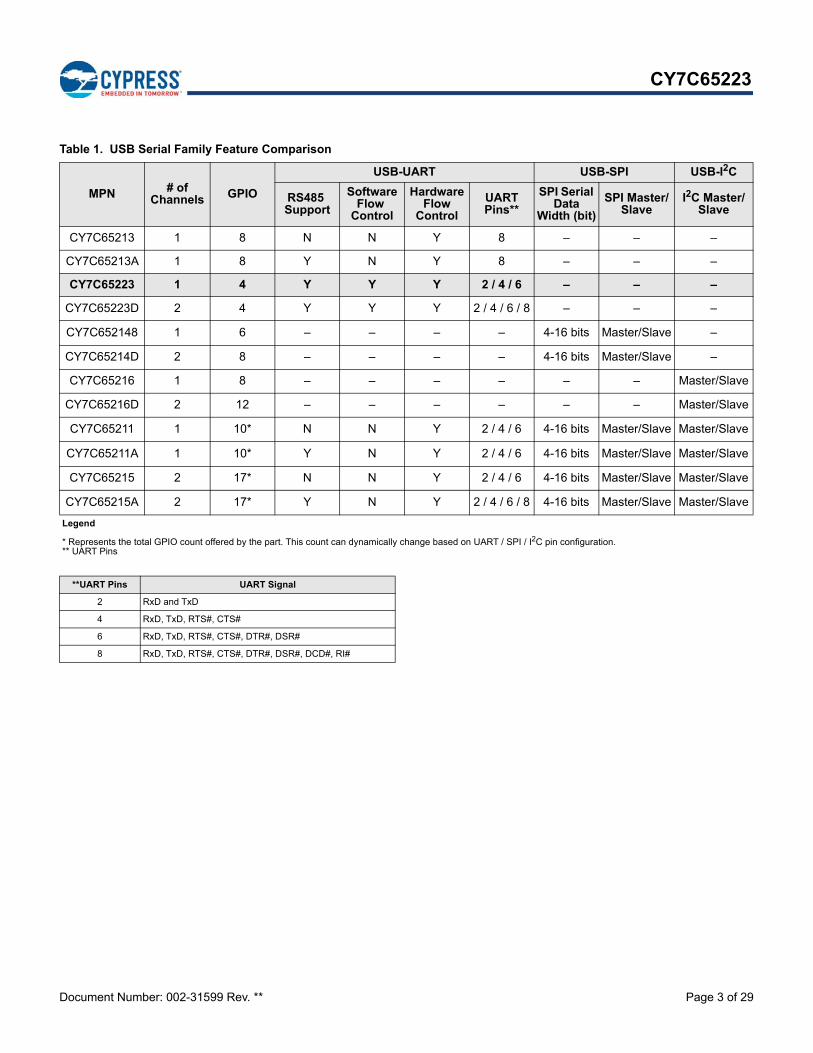
Table 1. USB Serial Family Feature Comparison
MPN # of Channels GPIO
USB-UART USB-SPI USB-I2C
RS485 Support
Software Flow
Control
Hardware Flow
Control
UART Pins **
SPI Serial Data
Width (bit)
SPI Master/ Slave
I2C Master/ Slave
CY7C65213 1 8 N N Y 8 – – –
CY7C65213A 1 8 Y N Y 8 – – –
CY7C65223 1 4 Y Y Y 2 / 4 / 6 – – –
CY7C65223D 2 4 Y Y Y 2 / 4 / 6 / 8 – – –
CY7C652148 1 6 – – – – 4-16 bits Master/Slave –
CY7C65214D 2 8 – – – – 4-16 bits Master/Slave –
CY7C65216 1 8 – – – – – – Master/Slave
CY7C65216D 2 12 – – – – – – Master/Slave
CY7C65211 1 10* N N Y 2 / 4 / 6 4-16 bits Master/Slave Master/Slave
CY7C65211A 1 10* Y N Y 2 / 4 / 6 4-16 bits Master/Slave Master/Slave
CY7C65215 2 17* N N Y 2 / 4 / 6 4-16 bits Master/Slave Master/Slave
CY7C65215A 2 17* Y N Y 2 / 4 / 6 / 8 4-16 bits Master/Slave Master/Slave
Legend
* Represents the total GPIO count offered by the part. This count can dynamically change based on UART / SPI / I2C pin configuration.** UART Pins
**UART Pins UART Signal
2 RxD and TxD
4 RxD, TxD, RTS#, CTS#
6 RxD, TxD, RTS#, CTS#, DTR#, DSR#
8 RxD, TxD, RTS#, CTS#, DTR#, DSR#, DCD#, RI#
Document Number: 002-31599 Rev. ** Page 4 of 29
CY7C65223
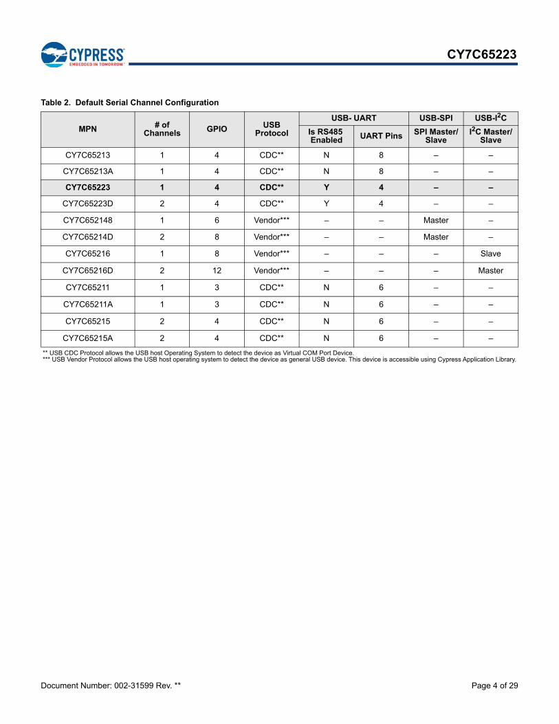
Table 2. Default Serial Channel Configuration
MPN # of Channels GPIO USB
Protocol
USB- UART USB-SPI USB-I2C
Is RS485 Enabled UART Pins SPI Master/
Slave I2C Master/
Slave
CY7C65213 1 4 CDC** N 8 – –
CY7C65213A 1 4 CDC** N 8 – –
CY7C65223 1 4 CDC** Y 4 – –
CY7C65223D 2 4 CDC** Y 4 – –
CY7C652148 1 6 Vendor*** – – Master –
CY7C65214D 2 8 Vendor*** – – Master –
CY7C65216 1 8 Vendor*** – – – Slave
CY7C65216D 2 12 Vendor*** – – – Master
CY7C65211 1 3 CDC** N 6 – –
CY7C65211A 1 3 CDC** N 6 – –
CY7C65215 2 4 CDC** N 6 – –
CY7C65215A 2 4 CDC** N 6 – –
** USB CDC Protocol allows the USB host Operating System to detect the device as Virtual COM Port Device.*** USB Vendor Protocol allows the USB host operating system to detect the device as general USB device. This device is accessible using Cypress Application Library.

Document Number: 002-31599 Rev. ** Page 5 of 29
CY7C65223
More Information
Cypress provides a wealth of data at www.cypress.com to help you to select the right device for your design, and to help you to quicklyand effectively integrate the device into your design. For a comprehensive list of resources, see the document USB-Serial BridgeController Product Overview.
Overview: USB Portfolio, USB Roadmap
USB 2.0 Product Selectors: USB-Serial Bridge Controller, USBto UART Controller (Gen I)
Knowledge Base Articles: Cypress offers a large number ofUSB knowledge base articles covering a broad range of topics,from basic to advanced level. Recommended knowledge basearticles for getting started with USB-Serial Bridge Controllerare: KBA85909 – Key Features of the Cypress® USB-Serial
Bridge Controller KBA85920 – USB-UART and USB-Serial KBA85921 – Replacing FT232R with CY7C65213
USB-UART LP Bridge Controller KBA85913 – Voltage supply range for USB-Serial KBA89355 – USB Serial Cypress Default VID and PID KBA92641 – USB-Serial Bridge Controller Managing I/Os
using API KBA92442 – Non-Standard Baud Rates in USB-Serial Bridge
Controllers KBA91366 – Binding a USB-Serial Device to a
Microsoft® CDC Driver KBA92551 – Testing a USB-Serial Bridge Controller Config-
ured as USB-UART with Linux®
KBA91299 – Interfacing an External I2C Device with the CY-USBS234/236 DVK
For complete list of knowledge base articles, click here.
Code Examples: USB Full-Speed
Development Kits: CYUSBS232, Cypress USB-UART LP Reference Design Kit CYUSBS234, Cypress USB-Serial (Single Channel) Devel-
opment Kit CYUSBS236, Cypress USB-Serial (Dual Channel) Develop-
ment Kit
Models: IBIS
Document Number: 002-31599 Rev. ** Page 6 of 29
CY7C65223
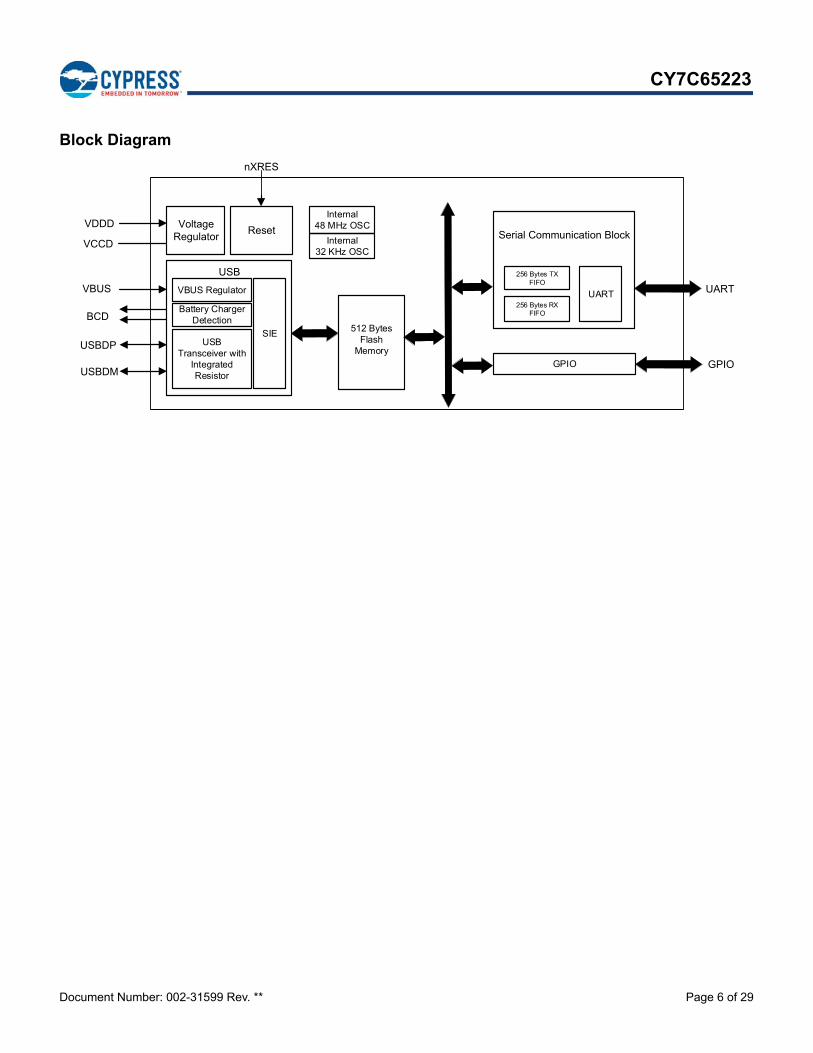
Block Diagram
USB Transceiver with
Integrated Resistor
Voltage Regulator
Internal48 MHz OSC
GPIO
USBDP
USBDM
Battery Charger Detection
SIE
USB
Internal32 KHz OSC
Reset Serial Communication Block
UART256 Bytes RX
FIFO
256 Bytes TX FIFO
nXRES
VDDD
VBUS
VCCD
512 Bytes Flash
Memory
VBUS Regulator UART
GPIO
BCD
Document Number: 002-31599 Rev. ** Page 7 of 29
CY7C65223
Contents
Functional Overview ........................................................ 8USB and Charger Detect ............................................. 8Serial Communication ................................................. 8GPIO Interface ............................................................ 8Default Configuration ................................................... 8Memory .......................................................................9System Resources ...................................................... 9Suspend and Resume ................................................. 9WAKEUP ..................................................................... 9Software ...................................................................... 9Internal Flash Configuration ...................................... 10
Electrical Specifications ................................................ 11Absolute Maximum Ratings ....................................... 11Operating Conditions ................................................. 11Device-Level Specifications ...................................... 11GPIO ......................................................................... 12nXRES ....................................................................... 13Flash Memory Specifications .................................... 13
Pin Description ............................................................... 14USB Power Configurations ............................................ 17
USB Bus-Powered Configuration .............................. 17
Self-Powered Configuration ...................................... 18USB Bus-Powered with Variable I/O Voltage ............ 19
Application Examples .................................................... 20USB to RS232 Bridge ................................................ 20USB to RS485 Bridge ................................................ 21Battery-Operated, Bus-Powered USB to MCU with Battery Charge Detection .................................. 22
Ordering Information ...................................................... 24Ordering Code Definitions ......................................... 24
Package Information ...................................................... 25Acronyms ........................................................................ 26Document Conventions ................................................. 26
Units of Measure ....................................................... 26Errata ............................................................................... 27Document History Page ................................................. 28Sales, Solutions, and Legal Information ...................... 29
Worldwide Sales and Design Support ....................... 29Products .................................................................... 29PSoC® Solutions ....................................................... 29Cypress Developer Community ................................. 29Technical Support ..................................................... 29
Document Number: 002-31599 Rev. ** Page 8 of 29
CY7C65223
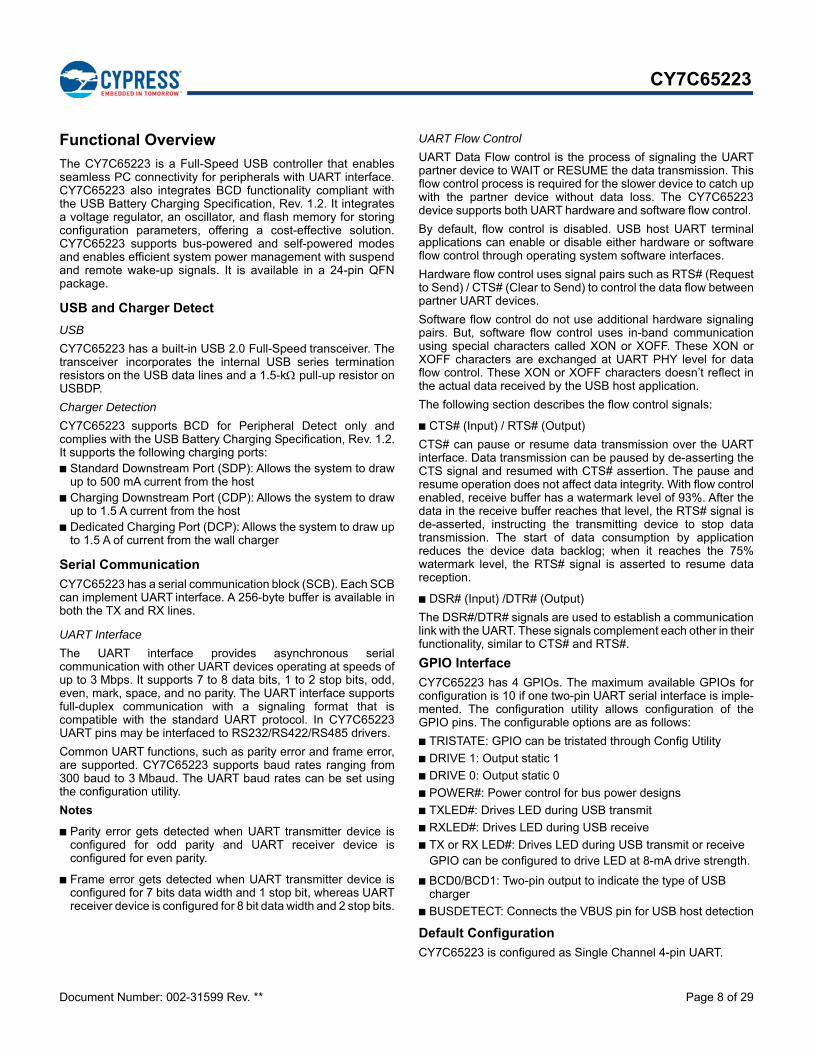
Functional Overview
The CY7C65223 is a Full-Speed USB controller that enablesseamless PC connectivity for peripherals with UART interface.CY7C65223 also integrates BCD functionality compliant withthe USB Battery Charging Specification, Rev. 1.2. It integratesa voltage regulator, an oscillator, and flash memory for storingconfiguration parameters, offering a cost-effective solution.CY7C65223 supports bus-powered and self-powered modesand enables efficient system power management with suspendand remote wake-up signals. It is available in a 24-pin QFNpackage.
USB and Charger Detect
USB
CY7C65223 has a built-in USB 2.0 Full-Speed transceiver. Thetransceiver incorporates the internal USB series terminationresistors on the USB data lines and a 1.5-k pull-up resistor onUSBDP.
Charger Detection
CY7C65223 supports BCD for Peripheral Detect only andcomplies with the USB Battery Charging Specification, Rev. 1.2.It supports the following charging ports: Standard Downstream Port (SDP): Allows the system to draw
up to 500 mA current from the host Charging Downstream Port (CDP): Allows the system to draw
up to 1.5 A current from the host Dedicated Charging Port (DCP): Allows the system to draw up
to 1.5 A of current from the wall charger
Serial Communication
CY7C65223 has a serial communication block (SCB). Each SCBcan implement UART interface. A 256-byte buffer is available inboth the TX and RX lines.
UART Interface
The UART interface provides asynchronous serialcommunication with other UART devices operating at speeds ofup to 3 Mbps. It supports 7 to 8 data bits, 1 to 2 stop bits, odd,even, mark, space, and no parity. The UART interface supportsfull-duplex communication with a signaling format that iscompatible with the standard UART protocol. In CY7C65223UART pins may be interfaced to RS232/RS422/RS485 drivers.
Common UART functions, such as parity error and frame error,are supported. CY7C65223 supports baud rates ranging from300 baud to 3 Mbaud. The UART baud rates can be set usingthe configuration utility.
Notes
Parity error gets detected when UART transmitter device isconfigured for odd parity and UART receiver device isconfigured for even parity.
Frame error gets detected when UART transmitter device isconfigured for 7 bits data width and 1 stop bit, whereas UARTreceiver device is configured for 8 bit data width and 2 stop bits.
UART Flow Control
UART Data Flow control is the process of signaling the UARTpartner device to WAIT or RESUME the data transmission. Thisflow control process is required for the slower device to catch upwith the partner device without data loss. The CY7C65223device supports both UART hardware and software flow control.
By default, flow control is disabled. USB host UART terminalapplications can enable or disable either hardware or softwareflow control through operating system software interfaces.
Hardware flow control uses signal pairs such as RTS# (Requestto Send) / CTS# (Clear to Send) to control the data flow betweenpartner UART devices.
Software flow control do not use additional hardware signalingpairs. But, software flow control uses in-band communicationusing special characters called XON or XOFF. These XON orXOFF characters are exchanged at UART PHY level for dataflow control. These XON or XOFF characters doesn’t reflect inthe actual data received by the USB host application.
The following section describes the flow control signals:
CTS# (Input) / RTS# (Output)
CTS# can pause or resume data transmission over the UARTinterface. Data transmission can be paused by de-asserting theCTS signal and resumed with CTS# assertion. The pause andresume operation does not affect data integrity. With flow controlenabled, receive buffer has a watermark level of 93%. After thedata in the receive buffer reaches that level, the RTS# signal isde-asserted, instructing the transmitting device to stop datatransmission. The start of data consumption by applicationreduces the device data backlog; when it reaches the 75%watermark level, the RTS# signal is asserted to resume datareception.
DSR# (Input) /DTR# (Output)
The DSR#/DTR# signals are used to establish a communicationlink with the UART. These signals complement each other in theirfunctionality, similar to CTS# and RTS#.
GPIO Interface
CY7C65223 has 4 GPIOs. The maximum available GPIOs forconfiguration is 10 if one two-pin UART serial interface is imple-mented. The configuration utility allows configuration of theGPIO pins. The configurable options are as follows:
TRISTATE: GPIO can be tristated through Config Utility
DRIVE 1: Output static 1
DRIVE 0: Output static 0
POWER#: Power control for bus power designs
TXLED#: Drives LED during USB transmit
RXLED#: Drives LED during USB receive
TX or RX LED#: Drives LED during USB transmit or receive GPIO can be configured to drive LED at 8-mA drive strength.
BCD0/BCD1: Two-pin output to indicate the type of USB charger
BUSDETECT: Connects the VBUS pin for USB host detection
Default Configuration
CY7C65223 is configured as Single Channel 4-pin UART.

Document Number: 002-31599 Rev. ** Page 9 of 29
CY7C65223
Memory
CY7C65223 has a 512-byte flash. Flash is used to store USBparameters, such as VID/PID, serial number, product andmanufacturer descriptors, which can be programmed by theconfiguration utility.
System Resources
Power System
CY7C65223 supports the USB Suspend mode to control powerusage. CY7C65223 operates in bus-powered or self-poweredmodes over a range of 3.15 to 5.5 V.
Clock System
CY7C65223 has a fully integrated clock with no external compo-nents required. The clock system is responsible for providingclocks to all subsystems.
Internal 48-MHz Oscillator
The internal 48-MHz oscillator is the primary source of internalclocking in CY7C65223.
Internal 32-kHz Oscillator
The internal 32-kHz oscillator is primarily used to generateclocks for peripheral operation in the USB Suspend mode.
Reset
The reset block ensures reliable power-on reset and brings thedevice back to the default known state. The nXRES (active low)pin can be used by the external devices to reset the CY7C65223.
Suspend and Resume
The CY7C65223 device asserts the SUSPEND pin when theUSB bus enters the suspend state. This helps in meeting thestringent suspend current requirement of the USB 2.0 specifi-cation, while using the device in bus-powered mode. The deviceresumes from the suspend state under either of the two followingconditions:
1. Any activity is detected on the USB bus
2. The WAKEUP pin is asserted to generate remote wakeup to the host
WAKEUP
The WAKEUP pin is used to generate the remote wakeup signalon the USB bus. The remote wakeup signal is sent only if thehost enables this feature through the SET_FEATURE request.The device communicates support for the remote wakeup to thehost through the configuration descriptor during the USBenumeration process. The CY7C65223 device allowsenabling/disabling and polarity of the remote wakeup featurethrough the configuration utility.
Software
Cypress delivers a complete set of software drivers and a config-uration utility to enable configuration of the product duringsystem development.
Drivers for Linux Operating Systems
Cypress provides a User Mode USB driver library (libcyusb-serial.so) that abstracts vendor commands for the UARTinterface and provides a simplified API interface for user applica-tions. This library uses the standard open-source libUSB libraryto enable USB communication. The Cypress serial librarysupports the USB plug-and-play feature using the Linux ‘udev’mechanism.
CY7C65223 supports the standard USB CDC UART classdriver, which is bundled with the Linux kernel.
Drivers for Mac OSx
Cypress delivers a dynamically linked shared library (CyUSB-Serial.dylib) based on libUSB, which enables communication tothe CY7C65223 device.
In addition, CY7C65223 supports native Mac OSx CDC UARTdriver.
Drivers for Windows Operating Systems
For Windows operating systems (XP, Vista, Win7, Win 8, andWin 8.1), Cypress delivers a user-mode dynamically linkedlibrary–CyUSBSerial DLL–that abstracts a vendor-specificinterface of the CY7C65223 devices and provides convenientAPIs to the user. It provides interface APIs for vendor-specificUART and class-specific APIs for PHDC.
USB-Serial Bridge Controller works with the Windows-standardUSB CDC class driver, when CY7C65223 is configured as CDCUSB to UART device. A virtual COM port driver–CyUSB-Serial.sys–is also delivered, which implements the USB CDCclass driver. The Cypress Windows drivers are Windowshardware certification kit-compliant.
These drivers are bound to device through WU (WindowsUpdate) services.
Cypress drivers also support Windows plug-and-play and powermanagement and USB Remote Wake-up.
Windows-CE Support
The CY7C65223 solution includes a CDC UART driver library forWindows-CE platforms.
Device Configuration Utility (Windows only)
A Windows-based configuration utility is available to configuredevice initialization parameters. This graphical user applicationprovides an interactive interface to define the boot parametersstored in the device flash.
This utility allows the user to save a user-selected configurationto text or xml formats. It also allows users to load a selectedconfiguration from text or xml formats. The configuration utilityallows the following operations:
View current device configuration
Select and configure UART, battery charging, and GPIOs
Configure USB VID, PID, and string descriptors
Save or Load configuration
You can download the free configuration utility and drivers atwww.cypress.com.
Document Number: 002-31599 Rev. ** Page 10 of 29
CY7C65223
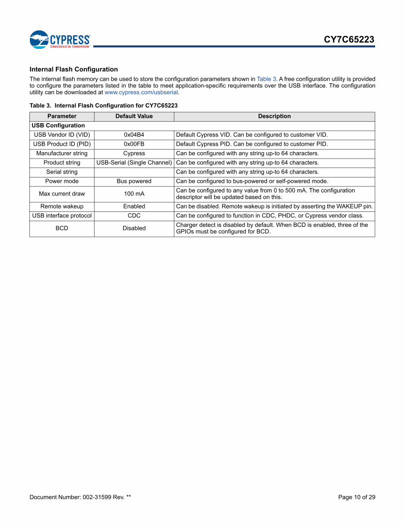
Internal Flash Configuration
The internal flash memory can be used to store the configuration parameters shown in Table 3. A free configuration utility is providedto configure the parameters listed in the table to meet application-specific requirements over the USB interface. The configurationutility can be downloaded at www.cypress.com/usbserial.
Table 3. Internal Flash Configuration for CY7C65223
Parameter Default Value Description
USB Configuration
USB Vendor ID (VID) 0x04B4 Default Cypress VID. Can be configured to customer VID.
USB Product ID (PID) 0x00FB Default Cypress PID. Can be configured to customer PID.
Manufacturer string Cypress Can be configured with any string up-to 64 characters.
Product string USB-Serial (Single Channel) Can be configured with any string up-to 64 characters.
Serial string Can be configured with any string up-to 64 characters.
Power mode Bus powered Can be configured to bus-powered or self-powered mode.
Max current draw 100 mA Can be configured to any value from 0 to 500 mA. The configuration descriptor will be updated based on this.
Remote wakeup Enabled Can be disabled. Remote wakeup is initiated by asserting the WAKEUP pin.
USB interface protocol CDC Can be configured to function in CDC, PHDC, or Cypress vendor class.
BCD Disabled Charger detect is disabled by default. When BCD is enabled, three of the GPIOs must be configured for BCD.
Document Number: 002-31599 Rev. ** Page 11 of 29
CY7C65223
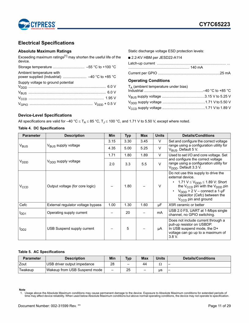
Electrical Specifications
Absolute Maximum Ratings
Exceeding maximum ratings[1] may shorten the useful life of thedevice.
Storage temperature ............................... –55 °C to +100 °C
Ambient temperature with power supplied (Industrial) ....................... –40 °C to +85 °C
Supply voltage to ground potential VDDD ............................................................................ 6.0 V
VBUS ............................................................................ 6.0 V
VCCD .......................................................................... 1.95 V
VGPIO .............................................................. VDDD + 0.5 V
Static discharge voltage ESD protection levels:
2.2-KV HBM per JESD22-A114
Latch-up current .................................................................... ............................................................... 140 mA
Current per GPIO .............................................................25 mA
Operating Conditions
TA (ambient temperature under bias) Industrial ..........................................................–40 °C to +85 °C
VBUS supply voltage ..........................................3.15 V to 5.25 V
VDDD supply voltage ..........................................1.71 V to 5.50 V
VCCD supply voltage ..........................................1.71 V to 1.89 V
Device-Level Specifications
All specifications are valid for –40 °C TA 85 °C, TJ 100 °C, and 1.71 V to 5.50 V, except where noted.
Table 4. DC Specifications
Parameter Description Min Typ Max Units Details/Conditions
VBUS VBUS supply voltage3.15 3.30 3.45 V Set and configure the correct voltage
range using a configuration utility for VBUS. Default 5 V.4.35 5.00 5.25 V
VDDD VDDD supply voltage
1.71 1.80 1.89 V Used to set I/O and core voltage. Set and configure the correct voltage range using a configuration utility for VDDD. Default 3.3 V.
2.0 3.3 5.5 V
VCCD Output voltage (for core logic) – 1.80 – V
Do not use this supply to drive the external device.
• 1.71 V VDDD 1.89 V: Short the VCCD pin with the VDDD pin
• VDDD > 2 V – connect a 1-µF capacitor (Cefc) between the VCCD pin and ground
Cefc External regulator voltage bypass 1.00 1.30 1.60 µF X5R ceramic or better
IDD1 Operating supply current – 20 – mA USB 2.0 FS, UART at 1-Mbps single channel, no GPIO switching.
IDD2 USB Suspend supply current – 5 – µA
Does not include current through a pull-up resistor on USBDP.In USB suspend mode, the D+ voltage can go up to a maximum of 3.8 V.
Table 5. AC Specifications
Parameter Description Min Typ Max Units Details/Conditions
Zout USB driver output impedance 28 – 44 –
Twakeup Wakeup from USB Suspend mode – 25 – µs –
Note1. Usage above the Absolute Maximum conditions may cause permanent damage to the device. Exposure to Absolute Maximum conditions for extended periods of
time may affect device reliability. When used below Absolute Maximum conditions but above normal operating conditions, the device may not operate to specification.

Document Number: 002-31599 Rev. ** Page 12 of 29
CY7C65223
GPIO
Table 6. GPIO DC Specifications
Parameter Description Min Typ Max Units Details/Conditions
VIH[2] Input voltage high threshold 0.7 × VDDD – – V CMOS Input
VIL Input voltage low threshold – – 0.3 × VDDD V CMOS Input
VIH[2] LVTTL input, VDDD< 2.7 V 0.7 × VDDD – – V –
VIL LVTTL input, VDDD < 2.7V – – 0.3 × VDDD V –
VIH[2] LVTTL input, VDDD > 2.7V 2 – – V –
VIL LVTTL input, VDDD > 2.7V – – 0.8 V –
VOH CMOS output voltage high level VDDD – 0.4 – – V IOH = 4 mA, VDDD = 5 V +/- 10%
VOH CMOS output voltage high level VDDD – 0.6 – – V IOH = 4 mA, VDDD = 3.3 V +/- 10%
VOH CMOS output voltage high level VDDD – 0.5 – – V IOH = 1 mA, VDDD = 1.8 V +/- 5%
VOL CMOS output voltage low level – – 0.4 V IOL = 8 mA, VDDD = 5 V +/- 10%
VOL CMOS output voltage low level – – 0.6 V IOL = 8 mA, VDDD = 3.3 V +/- 10%
VOL CMOS output voltage low level – – 0.6 V IOL = 4 mA, VDDD = 1.8 V +/- 5%
Rpullup Pull-up resistor 3.5 5.6 8.5 kΩ –
Rpulldown Pull-down resistor 3.5 5.6 8.5 kΩ –
IIL Input leakage current (absolute value) – – 2 nA 25 °C, VDDD = 3.0 V
CIN Input capacitance – – 7 pF –
Vhysttl Input hysteresis LVTTL; VDDD > 2.7 V 25 40 C mV –
Vhyscmos Input hysteresis CMOS 0.05 × VDDD – – mV –
Table 7. GPIO AC Specifications
Parameter Description Min Typ Max Units Details/Conditions
TRiseFast1 Rise Time in Fast mode 2 – 12 ns VDDD = 3.3 V/ 5.5 V, Cload = 25 pF
TFallFast1 Fall Time in Fast mode 2 – 12 ns VDDD = 3.3 V/ 5.5 V, Cload = 25 pF
TRiseSlow1 Rise Time in Slow mode 10 – 60 ns VDDD = 3.3 V/ 5.5 V, Cload = 25 pF
TFallSlow1 Fall Time in Slow mode 10 – 60 ns VDDD = 3.3 V/ 5.5 V, Cload = 25 pF
TRiseFast2 Rise Time in Fast mode 2 – 20 ns VDDD = 1.8 V, Cload = 25 pF
TFallFast2 Fall Time in Fast mode 20 – 100 ns VDDD = 1.8 V, Cload = 25 pF
TRiseSlow2 Rise Time in Slow mode 2 – 20 ns VDDD = 1.8 V, Cload = 25 pF
TFallSlow2 Fall Time in Slow mode 20 – 100 ns VDDD = 1.8 V, Cload = 25 pF
Note2. VIH must not exceed VDDD + 0.2 V.
Document Number: 002-31599 Rev. ** Page 13 of 29
CY7C65223
nXRES
Flash Memory Specifications
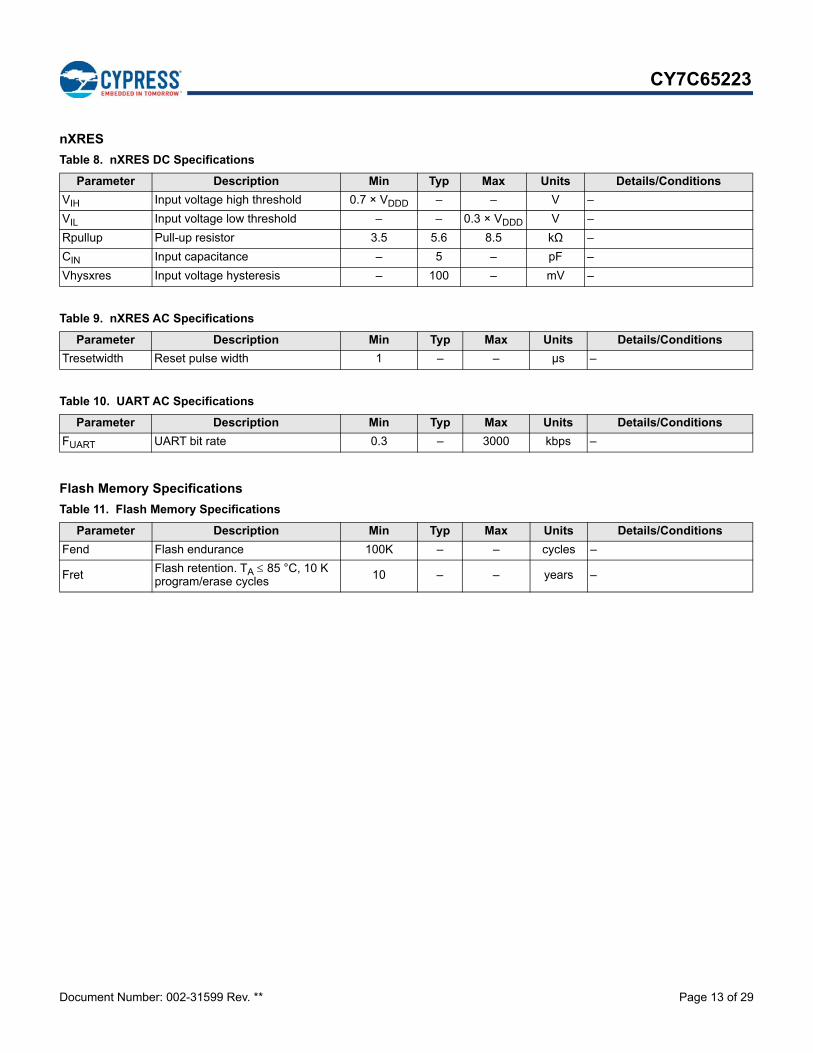
Table 8. nXRES DC Specifications
Parameter Description Min Typ Max Units Details/Conditions
VIH Input voltage high threshold 0.7 × VDDD – – V –
VIL Input voltage low threshold – – 0.3 × VDDD V –
Rpullup Pull-up resistor 3.5 5.6 8.5 kΩ –
CIN Input capacitance – 5 – pF –
Vhysxres Input voltage hysteresis – 100 – mV –
Table 9. nXRES AC Specifications
Parameter Description Min Typ Max Units Details/Conditions
Tresetwidth Reset pulse width 1 – – µs –
Table 10. UART AC Specifications
Parameter Description Min Typ Max Units Details/Conditions
FUART UART bit rate 0.3 – 3000 kbps –
Table 11. Flash Memory Specifications
Parameter Description Min Typ Max Units Details/Conditions
Fend Flash endurance 100K – – cycles –
FretFlash retention. TA 85 °C, 10 K program/erase cycles 10 – – years –
Document Number: 002-31599 Rev. ** Page 14 of 29
CY7C65223
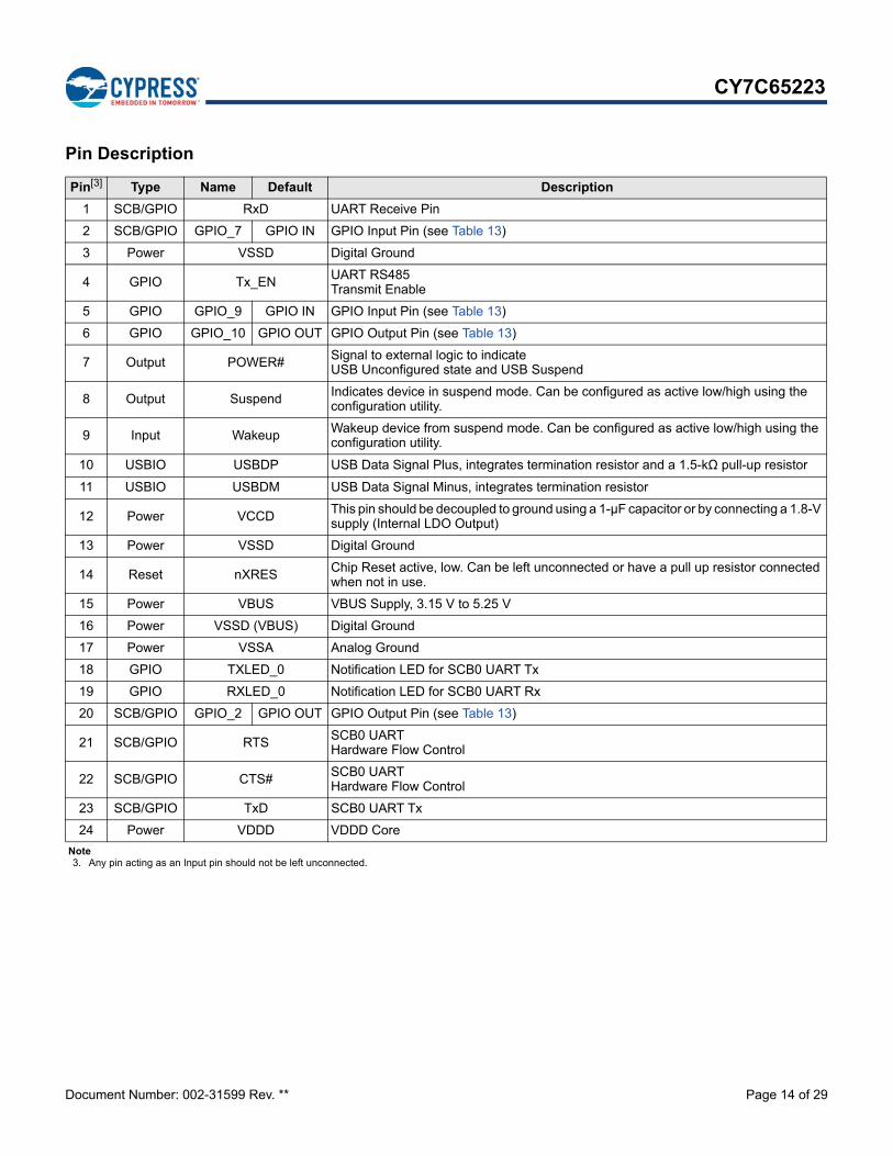
Pin Description
Pin[3] Type Name Default Description
1 SCB/GPIO RxD UART Receive Pin
2 SCB/GPIO GPIO_7 GPIO IN GPIO Input Pin (see Table 13)
3 Power VSSD Digital Ground
4 GPIO Tx_EN UART RS485 Transmit Enable
5 GPIO GPIO_9 GPIO IN GPIO Input Pin (see Table 13)
6 GPIO GPIO_10 GPIO OUT GPIO Output Pin (see Table 13)
7 Output POWER# Signal to external logic to indicate USB Unconfigured state and USB Suspend
8 Output SuspendIndicates device in suspend mode. Can be configured as active low/high using the configuration utility.
9 Input Wakeup Wakeup device from suspend mode. Can be configured as active low/high using the configuration utility.
10 USBIO USBDP USB Data Signal Plus, integrates termination resistor and a 1.5-kΩ pull-up resistor
11 USBIO USBDM USB Data Signal Minus, integrates termination resistor
12 Power VCCDThis pin should be decoupled to ground using a 1-µF capacitor or by connecting a 1.8-V supply (Internal LDO Output)
13 Power VSSD Digital Ground
14 Reset nXRES Chip Reset active, low. Can be left unconnected or have a pull up resistor connected when not in use.
15 Power VBUS VBUS Supply, 3.15 V to 5.25 V
16 Power VSSD (VBUS) Digital Ground
17 Power VSSA Analog Ground
18 GPIO TXLED_0 Notification LED for SCB0 UART Tx
19 GPIO RXLED_0 Notification LED for SCB0 UART Rx
20 SCB/GPIO GPIO_2 GPIO OUT GPIO Output Pin (see Table 13)
21 SCB/GPIO RTS SCB0 UART Hardware Flow Control
22 SCB/GPIO CTS#SCB0 UART Hardware Flow Control
23 SCB/GPIO TxD SCB0 UART Tx
24 Power VDDD VDDD Core
Note3. Any pin acting as an Input pin should not be left unconnected.

Document Number: 002-31599 Rev. ** Page 15 of 29
CY7C65223
Figure 2. 24-pin QFN Pinout
Legend
CY7C65223-24QFNTop View
RxD
GPIO_7
VSSD
Tx_EN
GPIO_9
GPIO_10
1
2
3
4
5
6
VD
DD
TxD
CT
S#
RT
S
GP
IO_2
RX
LED
_0
24
23
22
21
20
19
7 8 9 10
11
12
PO
WE
R#
SU
SP
EN
D
WA
KE
UP
US
BD
P
US
BD
M
VC
CD
18
17
16
15
14
13
TXLED_0
VSSA
VSSD
VBUS
nXRES
VSSD
Table 12. Serial Communication Block Configuration
Pin Serial PortMode 0[4] Mode 1 Mode 2
6-pin UART 4-pin UART 2-pin UART
1 SCB_0 RxD RxD RxD
20 SCB_1 DSR# GPIO_2 GPIO_2
21 SCB_2 RTS# RTS# GPIO_3
22 SCB_3 CTS# CTS# GPIO_4
23 SCB_4 TxD TxD TxD
2 SCB_5 DTR# GPIO_7 GPIO_7Note4. The device is configured in Mode 0 as the default. Other modes can be configured using the configuration utility provided by Cypress.
GPIO
SCB

Document Number: 002-31599 Rev. ** Page 16 of 29
CY7C65223
Table 13. GPIO Configuration[5]
GPIO Configuration Option Description
TRISTATE I/O tristated
DRIVE 1 Output static 1
DRIVE 0 Output static 0
POWER#
This output is used to control power to an external logic through a switch to cut power off during an unconfigured USB device and USB suspend.0 - USB device in Configured state1 - USB device in Unconfigured state or during USB suspend mode
TXLED# Drives LED during USB transmit
RXLED# Drives LED during USB receive
TX or RX LED# Drives LED during USB transmit or receive
BCD0BCD1
Configurable battery charger detect pins to indicate the type of USB charger (SDP, CDP, or DCP) Configuration example:00 - Draw up to 100 mA (unconfigured state)01 - SDP (up to 500 mA)10 - CDP/DCP (up to 1.5 A)11 - Suspend (up to 2.5 mA)This truth table can be configured using a configuration utility
BUSDETECTVBUS detection. Connect the VBUS to this pin through a resistor network for VBUS detection when using the BCD feature (refer to Figure 10, Figure 11, and Figure 12).
Note5. These signal options can be configured on any of the available GPIO pins using the configuration utility provided by Cypress.
Document Number: 002-31599 Rev. ** Page 17 of 29
CY7C65223
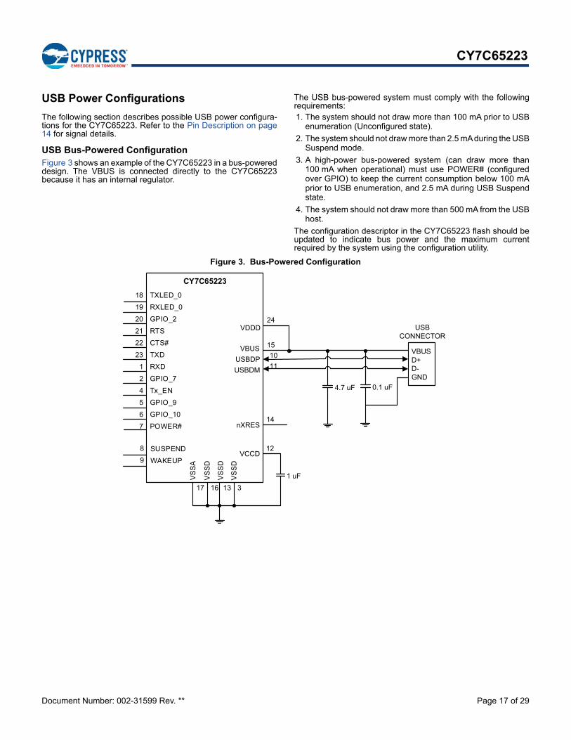
USB Power Configurations
The following section describes possible USB power configura-tions for the CY7C65223. Refer to the Pin Description on page14 for signal details.
USB Bus-Powered ConfigurationFigure 3 shows an example of the CY7C65223 in a bus-powereddesign. The VBUS is connected directly to the CY7C65223because it has an internal regulator.
The USB bus-powered system must comply with the followingrequirements:1. The system should not draw more than 100 mA prior to USB
enumeration (Unconfigured state).
2. The system should not draw more than 2.5 mA during the USBSuspend mode.
3. A high-power bus-powered system (can draw more than100 mA when operational) must use POWER# (configuredover GPIO) to keep the current consumption below 100 mAprior to USB enumeration, and 2.5 mA during USB Suspendstate.
4. The system should not draw more than 500 mA from the USBhost.
The configuration descriptor in the CY7C65223 flash should beupdated to indicate bus power and the maximum currentrequired by the system using the configuration utility.
Figure 3. Bus-Powered Configuration
USB CONNECTOR
VBUSD+D-GND
VBUS
VCCD
1 uF
0.1 uF
CY7C65223
USBDP
USBDM
VS
SD
nXRES
VDDD
VS
SA
15
24
14
10
11
12
317
VS
SD
VS
SD
1316
4.7 uF
18
19
20
21
22
23
1
2
4
5
6
7
TXLED_0
RXLED_0
GPIO_2
RTS
CTS#
TXD
RXD
GPIO_7
Tx_EN
GPIO_9
GPIO_10
POWER#
SUSPEND
WAKEUP
8
9

Document Number: 002-31599 Rev. ** Page 18 of 29
CY7C65223
Self-Powered ConfigurationFigure 4 shows an example of CY7C65223 in a self-powereddesign. A self-powered system does not use the VBUS from thehost to power the system, but it has its own power supply. Aself-powered system has no restriction on current consumptionbecause it does not draw any current from the VBUS.When the VBUS is present, CY7C65223 enables an internal,1.5-k pull-up resistor on USBDP. When the VBUS is absent(USB host is powered down), CY7C65223 removes the 1.5-kpull-up resistor on USBDP. This ensures that no current flowsfrom the USBDP to the USB host through a 1.5-k pull-upresistor, to comply with the USB 2.0 specification.
When reset is asserted to CY7C65223, all the I/O pins aretristated.The configuration descriptor in the CY7C65223 flash should beupdated to indicate self-power using the configuration utility.
Figure 4. Self-Powered Configuration
USB CONNECTOR
VBUSD+D-GND
VBUS
USBDP
USBDM
nXRES
VDDD
15
24
14
10
11
3.3 V
VCCD
1 uFVS
SD
VS
SA
12
317
VS
SD
VS
SD
1316
CY7C65223
3.3 V
4.7 KΩ
10 KΩ
18
19
20
21
22
23
1
2
4
5
6
7
TXLED_0
RXLED_0
GPIO_2
RTS
CTS#
TXD
RXD
GPIO_7
Tx_EN
GPIO_9
GPIO_10
POWER#
SUSPEND
WAKEUP
8
9
4.7 uF 0.1 uF
Document Number: 002-31599 Rev. ** Page 19 of 29
CY7C65223
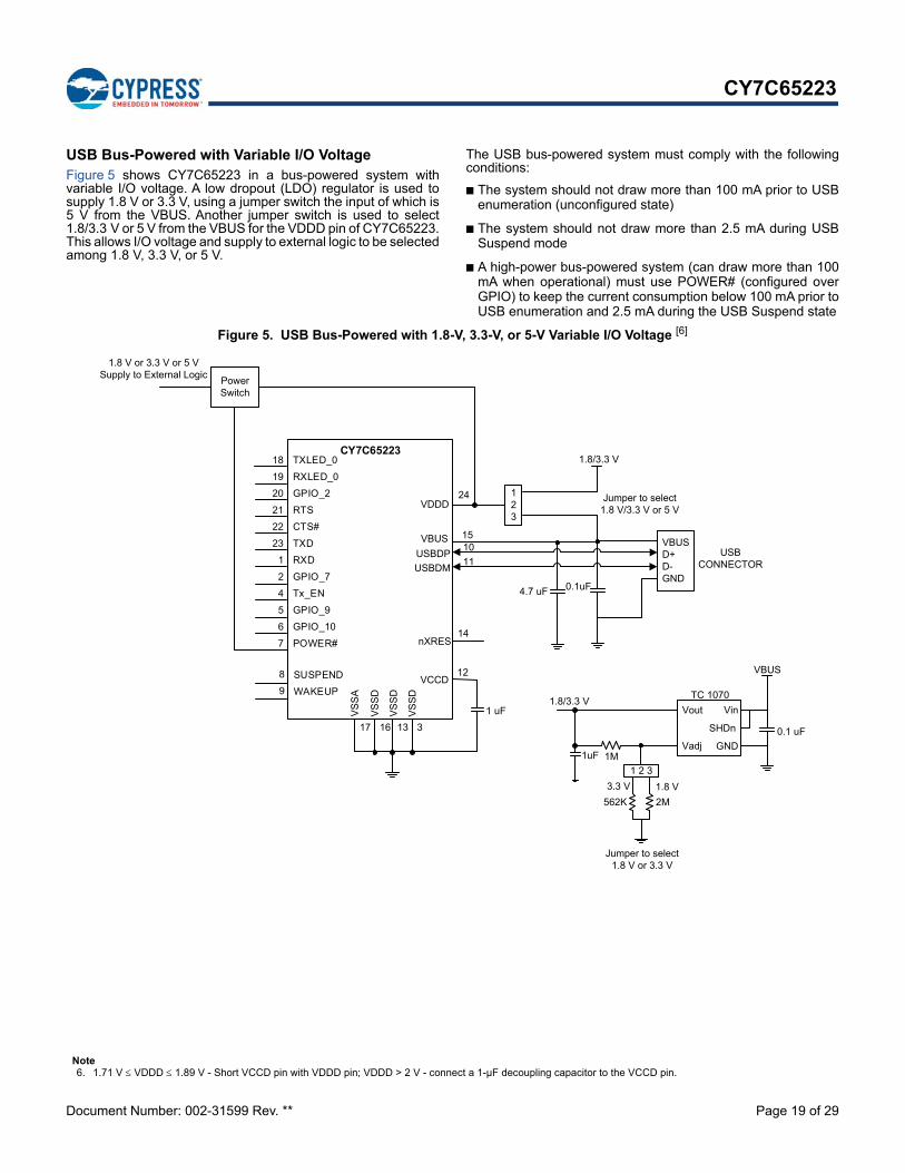
USB Bus-Powered with Variable I/O VoltageFigure 5 shows CY7C65223 in a bus-powered system withvariable I/O voltage. A low dropout (LDO) regulator is used tosupply 1.8 V or 3.3 V, using a jumper switch the input of which is5 V from the VBUS. Another jumper switch is used to select1.8/3.3 V or 5 V from the VBUS for the VDDD pin of CY7C65223.This allows I/O voltage and supply to external logic to be selectedamong 1.8 V, 3.3 V, or 5 V.
The USB bus-powered system must comply with the followingconditions:
The system should not draw more than 100 mA prior to USBenumeration (unconfigured state)
The system should not draw more than 2.5 mA during USBSuspend mode
A high-power bus-powered system (can draw more than 100mA when operational) must use POWER# (configured overGPIO) to keep the current consumption below 100 mA prior toUSB enumeration and 2.5 mA during the USB Suspend state
Figure 5. USB Bus-Powered with 1.8-V, 3.3-V, or 5-V Variable I/O Voltage [6]
USB CONNECTOR
VBUSD+D-GND
Vin
GND
SHDn
Vout
Vadj
Jumper to select1.8 V or 3.3 V
VBUS
0.1 uF
TC 1070
1uF 1M
1 2 3
562K 2M
3.3 V 1.8 V
1 2 3
1.8/3.3 V
1.8/3.3 V
1.8 V or 3.3 V or 5 V Supply to External Logic
Jumper to select1.8 V/3.3 V or 5 V
Power Switch
VBUS
USBDP
USBDM
nXRES
VDDD
15
24
14
10
11
VCCD
1 uFVS
SD
VS
SA
12
317
VS
SD
VS
SD
1316
CY7C65223
4.7 uF
18
19
20
21
22
23
1
2
4
5
6
7
TXLED_0
RXLED_0
GPIO_2
RTS
CTS#
TXD
RXD
GPIO_7
Tx_EN
GPIO_9
GPIO_10
POWER#
SUSPEND
WAKEUP
8
9
0.1uF
Note6. 1.71 V VDDD 1.89 V - Short VCCD pin with VDDD pin; VDDD > 2 V - connect a 1-µF decoupling capacitor to the VCCD pin.
Document Number: 002-31599 Rev. ** Page 20 of 29
CY7C65223
Application Examples
The following section provides CY7C65223 applicationexamples.
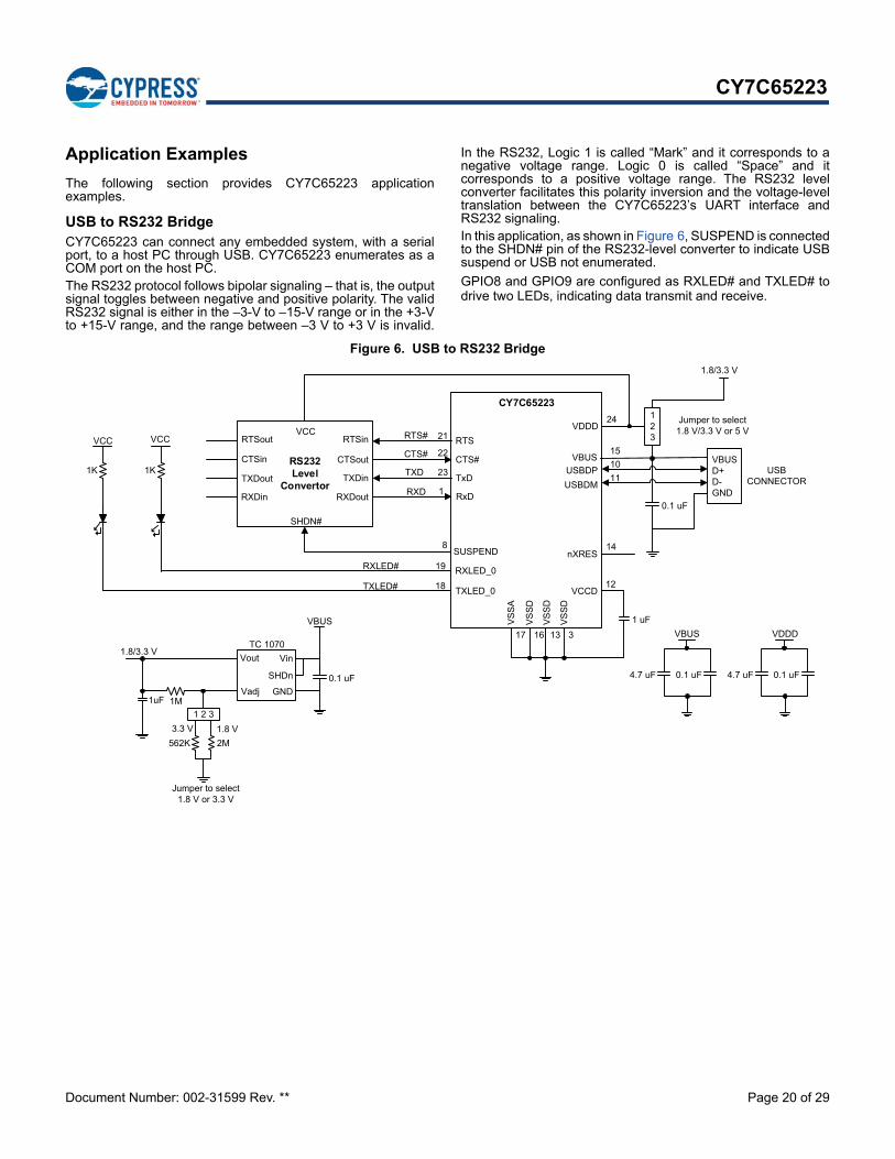
USB to RS232 BridgeCY7C65223 can connect any embedded system, with a serialport, to a host PC through USB. CY7C65223 enumerates as aCOM port on the host PC.The RS232 protocol follows bipolar signaling – that is, the outputsignal toggles between negative and positive polarity. The validRS232 signal is either in the –3-V to –15-V range or in the +3-Vto +15-V range, and the range between –3 V to +3 V is invalid.
In the RS232, Logic 1 is called “Mark” and it corresponds to anegative voltage range. Logic 0 is called “Space” and itcorresponds to a positive voltage range. The RS232 levelconverter facilitates this polarity inversion and the voltage-leveltranslation between the CY7C65223’s UART interface andRS232 signaling.In this application, as shown in Figure 6, SUSPEND is connectedto the SHDN# pin of the RS232-level converter to indicate USBsuspend or USB not enumerated.
GPIO8 and GPIO9 are configured as RXLED# and TXLED# todrive two LEDs, indicating data transmit and receive.
Figure 6. USB to RS232 Bridge
USB CONNECTOR
VBUSD+D-GND
0.1 uF
RS232 Level
Convertor
RTSin
CTSout
TXDin
RXDout
RTSout
CTSin
TXDout
RXDin
1K
TXLED#
RXLED#
1K
VCC VCC
SHDN#
VBUS
VCCD
1 uF
CY7C65223
USBDP
USBDM
VS
SD
nXRES
VDDD
SUSPEND
RTS
CTS#
VS
SA
TxD
RxD
15
14
10
11
12
317
8
22
VS
SD
VS
SD
1316
21
1
23
RXD
TXD
CTS#
RTS#
TXLED_0
RXLED_0
18
19
Vin
GND
SHDn
Vout
Vadj
Jumper to select1.8 V or 3.3 V
VBUS
0.1 uF
TC 1070
1uF 1M
1 2 3
562K 2M
3.3 V 1.8 V
1.8/3.3 V
24 1 2 3
1.8/3.3 V
Jumper to select1.8 V/3.3 V or 5 VVCC
4.7 uF 0.1 uF
VBUS
4.7 uF 0.1 uF
VDDD

Document Number: 002-31599 Rev. ** Page 21 of 29
CY7C65223
USB to RS485 BridgeCY7C65223 can be configured as USB to UART interface. ThisUART interface operates at TTL level and it can be converted toRS485 interface using a GPIO and any half duplex RS485transceiver IC (to convert TTL level to RS485 level) as shown inFigure 7. This GPIO (TXDEN) enables or disables thetransmission of data through RS485 transceiver IC based onavailability of character in UART buffer of CY7C65223. ThisGPIO can be configured using Cypress USB-SerialConfiguration utility. Figure 8 shows timing diagram of this GPIO.
RS485 is a multi-drop network – i.e. many devices cancommunicate with each other over a single two wire cableconnection. The RS485 cable requires to be terminated at eachend of the cable.
Figure 7. USB to RS485 Bridge
Figure 8. RS485 GPIO (TXDEN) Timing Diagram
USB CONNECTOR
VBUSD+D-GND
0.1 uF
RS485Level
ConvertorTXDin
RXDout
TXDout
RXDin
1K1K
VCC VCC
TXDEN
VBUS
VCCD
1 uF
CY7C65223
USBDP
USBDM
VS
SD
nXRES
VDDD
Tx_EN
RTS
CTS#
VS
SA
TxD
RxD
15
14
10
11
12
317
4
22
VS
SD
VS
SD
1316
21
1
23
RXD
TXD
TXLED_0
RXLED_0
18
19
Vin
GND
SHDn
Vout
Vadj
Jumper to select1.8 V or 3.3 V
VBUS
0.1 uF
TC 1070
1uF 1M
1 2 3
562K 2M
3.3 V 1.8 V
1.8/3.3 V
24 1 2 3
1.8/3.3 V
Jumper to select1.8 V/3.3 V or 5 VVCC
GND
4.7 uF 0.1 uF
VBUS
4.7 uF 0.1 uF
VDDD
TXDEN
TXD MSB LSB
LSBMSBRXD
Document Number: 002-31599 Rev. ** Page 22 of 29
CY7C65223
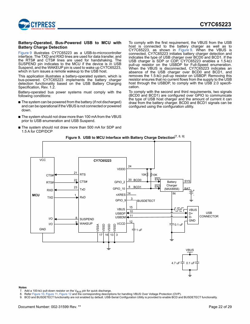
Battery-Operated, Bus-Powered USB to MCU withBattery Charge DetectionFigure 9 illustrates CY7C65223 as a USB-to-microcontrollerinterface. The TXD and RXD lines are used for data transfer, andthe RTS# and CTS# lines are used for handshaking. TheSUSPEND pin indicates to the MCU if the device is in USBSuspend, and the WAKEUP pin is used to wake up CY7C65223,which in turn issues a remote wakeup to the USB host.This application illustrates a battery-operated system, which isbus-powered. CY7C65223 implements the battery chargerdetection functionality based on the USB Battery ChargingSpecification, Rev. 1.2.Battery-operated bus power systems must comply with thefollowing conditions:
The system can be powered from the battery (if not discharged)and can be operational if the VBUS is not connected or powereddown.
The system should not draw more than 100 mA from the VBUSprior to USB enumeration and USB Suspend.
The system should not draw more than 500 mA for SDP and1.5 A for CDP/DCP
To comply with the first requirement, the VBUS from the USBhost is connected to the battery charger as well as toCY7C65223, as shown in Figure 9. When the VBUS isconnected, CY7C65223 initiates battery charger detection andindicates the type of USB charger over BCD0 and BCD1. If theUSB charger is SDP or CDP, CY7C65223 enables a 1.5-kpull-up resistor on the USBDP for Full-Speed enumeration.When the VBUS is disconnected, CY7C65223 indicates anabsence of the USB charger over BCD0 and BCD1, andremoves the 1.5-k pull-up resistor on USBDP. Removing thisresistor ensures that no current flows from the supply to the USBhost through the USBDP, to comply with the USB 2.0 specifi-cation.To comply with the second and third requirements, two signals(BCD0 and BCD1) are configured over GPIO to communicatethe type of USB host charger and the amount of current it candraw from the battery charger. BCD0 and BCD1 signals can beconfigured using the configuration utility.
Figure 9. USB to MCU Interface with Battery Charge Detection[7, 8, 9]
BAT
SYS
10K
USB CONNECTOR
VBUSD+D-GND
0.1 uF
10K
BCD0
BCD1
MCU
VCC
TXD
CTS#
RTS#
RXD
I/O
GND
I/O
EN2
IN
EN1Battery Charger
(MAX8856)
VBUS
USBDPUSBDM
nXRES
VDDD
15
24
14
10
11
VCCD
1 uFVS
SD
SUSPEND
WAKEUP
RTS
CTS# GPIO_2
VS
SA
GPIO_10TxD
RxD
12
317
8
22
VS
SD
VS
SD
1316
6
21
9
20
23
CY7C65223
1
OVP
4.7 uF 0.1 uF
VBUS
+
-
BUSDETECTGPIO_9 3
Notes7. Add a 100-k pull-down resistor on the VBUS pin for quick discharge.8. Refer Figure 10, Figure 11, Figure 12 and the corresponding descriptions for handling VBUS Over Voltage Protection (OVP).9. BCD and BUSDETECT functionality are not enabled by default. USB-Serial Configuration Utility is provided to enable BCD and BUSDETECT functionality.
Document Number: 002-31599 Rev. ** Page 23 of 29
CY7C65223
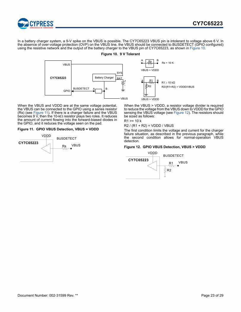
In a battery charger system, a 9-V spike on the VBUS is possible. The CY7C65223 VBUS pin is intolerant to voltage above 6 V. Inthe absence of over-voltage protection (OVP) on the VBUS line, the VBUS should be connected to BUSDETECT (GPIO configured)using the resistive network and the output of the battery charger to the VBUS pin of CY7C65223, as shown in Figure 10.
Figure 10. 9 V Tolerant
When the VBUS and VDDD are at the same voltage potential,the VBUS can be connected to the GPIO using a series resistor(Rs) (see Figure 11). If there is a charger failure and the VBUSbecomes 9 V, then the 10-k resistor plays two roles. It reducesthe amount of current flowing into the forward-biased diodes inthe GPIO, and it reduces the voltage seen on the pad.
Figure 11. GPIO VBUS Detection, VBUS = VDDD
When the VBUS > VDDD, a resistor voltage divider is requiredto reduce the voltage from the VBUS down to VDDD for the GPIOsensing the VBUS voltage (see Figure 12). The resistors shouldbe sized as follows:R1 >= 10 kR2 / (R1 + R2) = VDDD / VBUSThe first condition limits the voltage and current for the chargerfailure situation, as described in the previous paragraph, whilethe second condition allows for normal-operation VBUSdetection.
Figure 12. GPIO VBUS Detection, VBUS > VDDD
B
Battery Charger BAT
SYS
CY7C65223
VBUS
GPIOBUSDETECT
Rs
A
BA
R1 BA
R2
VBUS = VDDD
VBUS > VDDD
R1 ≥ 10 kΩ
R2/(R1+R2) = VDDD/VBUS
Rs = 10 K
VBUS
+
-
Rs VBUS
VDDDBUSDETECT
CY7C65223
R1 VBUS
R2
VDDD
CY7C65223BUSDETECT
Document Number: 002-31599 Rev. ** Page 24 of 29
CY7C65223
Ordering Information
Table 14 lists the key package features and ordering codes of the CY7C65223. For more information, contact your local salesrepresentative.
Ordering Code Definitions
Table 14. Key Features and Ordering Information
Package Ordering Code Operating Range
24-pin QFN (4.00 × 4.00 × 0.55 mm, 0.5 mm pitch) (Pb-free) CY7C65223-24LTXI Industrial
24-pin QFN (4.00 × 4.00 × 0.55 mm, 0.5 mm pitch) (Pb-free) – Tape and Reel CY7C65223-24LTXIT Industrial
X = blank or T blank = Tray; T = Tape and Reel
Temperature Range: I = Industrial
Pb-free
Package Type: LT = QFN
Number of pins: 24 pins
Part Number: XXX = 223
Family Code: 65 = USB Hubs
Technology Code: C = CMOS
Marketing Code: 7 = Cypress products
Company ID: CY = Cypress
CCY 65 I- 24 XXXX7 XX X
Document Number: 002-31599 Rev. ** Page 25 of 29
CY7C65223
Package Information
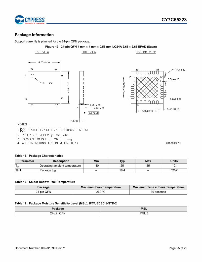
Support currently is planned for the 24-pin QFN package.
Figure 13. 24-pin QFN 4 mm 4 mm 0.55 mm LQ24A 2.65 2.65 EPAD (Sawn)
001-13937 *H
Table 15. Package Characteristics
Parameter Description Min Typ Max Units
TA Operating ambient temperature –40 25 85 °C
THJ Package JA – 18.4 – °C/W
Table 16. Solder Reflow Peak Temperature
Package Maximum Peak Temperature Maximum Time at Peak Temperature
24-pin QFN 260 °C 30 seconds
Table 17. Package Moisture Sensitivity Level (MSL), IPC/JEDEC J-STD-2
Package MSL
24-pin QFN MSL 3
Document Number: 002-31599 Rev. ** Page 26 of 29
CY7C65223
Acronyms Document Conventions
Units of MeasureTable 18. Acronyms Used in this Document
Acronym Description
BCD battery charger detection
CDC communication driver class
CDP charging downstream port
DCP dedicated charging port
DLL dynamic link library
ESD electrostatic discharge
GPIO general purpose input/output
HBM human-body model
MCU microcontroller unit
OSC oscillator
PHDC personal health care device class
PID product identification
SCB serial communication block
SDP standard downstream port
SIE serial interface engine
VCOM virtual communication port
USB Universal Serial Bus
UART universal asynchronous receiver transmitter
VID vendor identification
Table 19. Units of Measure
Symbol Unit of Measure
C degree Celsius
DMIPS Dhrystone million instructions per second
k kilo-ohm
KB kilobyte
kHz kilohertz
kV kilovolt
Mbps megabits per second
MHz megahertz
mm millimeter
V volt
Document Number: 002-31599 Rev. ** Page 27 of 29
CY7C65223
Errata
This section describes the errata for the CY7C65223 USB-Serial family. Details include errata trigger conditions, scope of impact, andavailable workaround.
Contact your local Cypress Sales Representative if you have questions.
Part Numbers Affected
Qualification Status
Production
Errata Summary
The following table defines the errata applicability to available USB-Serial devices.
Part Number Device Characteristics
CY7C65223 All Variants
Items Affected Part Number Fix Status
[1.] USB-Serial does not report UART Frame errors. CY7C65223 No Fix
[2.] USB-Serial does not report MARK or SPACE Parity errors. CY7C65223 No Fix
1. USB-Serial does not report UART Frame errors.
Problem Definition USB-Serial does not report UART Frame Errors while receiving UART data when the number of stopbits is set as 1.
Parameters Affected NA
Trigger Condition(s) USB-Serial fails to report a UART Frame error when the number of stop bits is set as 1. It correctlyreports the error when the stop bits is not 1.
Scope of Impact No impact
WorkaroundNo workaround. In general, applications using UART will have to include checksum or CRC in the data to ensure frame integrity.
Fix Status No fix
2. USB-Serial does not report MARK or SPACE Parity errors.
Problem DefinitionUSB-Serial does not report UART Parity error while receiving the data when configured for MARK orSPACE parity.
Parameters Affected NA
Trigger Condition(s)USB Serial fails to report UART Parity errors while receiving data when configured for MARK or SPACEparity. Note that USB-Serial detects parity errors when configured for ODD or EVEN parity settings.
Scope of Impact No impact
WorkaroundNo workaround. In general, applications using UART will have to include checksum or CRC in the data to ensure frame integrity.
Fix Status No fix
Document Number: 002-31599 Rev. ** Page 28 of 29
CY7C65223
Document History Page
Document Title: CY7C65223, USB-UART Single Channel Bridge ControllerDocument Number: 002-31599
Revision ECN Submission Date Description of Change
** 7021631 11/26/2020 Final datasheet to NSO.
Document Number: 002-31599 Rev. ** Revised November 26, 2020 Page 29 of 29
© Cypress Semiconductor Corporation, 2020. This document is the property of Cypress Semiconductor Corporation and its subsidiaries ("Cypress"). This document, including any software or firmwareincluded or referenced in this document ("Software"), is owned by Cypress under the intellectual property laws and treaties of the United States and other countries worldwide. Cypress reserves allrights under such laws and treaties and does not, except as specifically stated in this paragraph, grant any license under its patents, copyrights, trademarks, or other intellectual property rights. If theSoftware is not accompanied by a license agreement and you do not otherwise have a written agreement with Cypress governing the use of the Software, then Cypress hereby grants you a personal,non-exclusive, nontransferable license (without the right to sublicense) (1) under its copyright rights in the Software (a) for Software provided in source code form, to modify and reproduce the Softwaresolely for use with Cypress hardware products, only internally within your organization, and (b) to distribute the Software in binary code form externally to end users (either directly or indirectly throughresellers and distributors), solely for use on Cypress hardware product units, and (2) under those claims of Cypress's patents that are infringed by the Software (as provided by Cypress, unmodified)to make, use, distribute, and import the Software solely for use with Cypress hardware products. Any other use, reproduction, modification, translation, or compilation of the Software is prohibited.
TO THE EXTENT PERMITTED BY APPLICABLE LAW, CYPRESS MAKES NO WARRANTY OF ANY KIND, EXPRESS OR IMPLIED, WITH REGARD TO THIS DOCUMENT OR ANY SOFTWAREOR ACCOMPANYING HARDWARE, INCLUDING, BUT NOT LIMITED TO, THE IMPLIED WARRANTIES OF MERCHANTABILITY AND FITNESS FOR A PARTICULAR PURPOSE. No computingdevice can be absolutely secure. Therefore, despite security measures implemented in Cypress hardware or software products, Cypress shall have no liability arising out of any security breach, suchas unauthorized access to or use of a Cypress product. CYPRESS DOES NOT REPRESENT, WARRANT, OR GUARANTEE THAT CYPRESS PRODUCTS, OR SYSTEMS CREATED USINGCYPRESS PRODUCTS, WILL BE FREE FROM CORRUPTION, ATTACK, VIRUSES, INTERFERENCE, HACKING, DATA LOSS OR THEFT, OR OTHER SECURITY INTRUSION (collectively, "SecurityBreach"). Cypress disclaims any liability relating to any Security Breach, and you shall and hereby do release Cypress from any claim, damage, or other liability arising from any Security Breach. Inaddition, the products described in these materials may contain design defects or errors known as errata which may cause the product to deviate from published specifications. To the extent permittedby applicable law, Cypress reserves the right to make changes to this document without further notice. Cypress does not assume any liability arising out of the application or use of any product orcircuit described in this document. Any information provided in this document, including any sample design information or programming code, is provided only for reference purposes. It is theresponsibility of the user of this document to properly design, program, and test the functionality and safety of any application made of this information and any resulting product. "High-Risk Device"means any device or system whose failure could cause personal injury, death, or property damage. Examples of High-Risk Devices are weapons, nuclear installations, surgical implants, and othermedical devices. "Critical Component" means any component of a High-Risk Device whose failure to perform can be reasonably expected to cause, directly or indirectly, the failure of the High-RiskDevice, or to affect its safety or effectiveness. Cypress is not liable, in whole or in part, and you shall and hereby do release Cypress from any claim, damage, or other liability arising from any use ofa Cypress product as a Critical Component in a High-Risk Device. You shall indemnify and hold Cypress, its directors, officers, employees, agents, affiliates, distributors, and assigns harmless fromand against all claims, costs, damages, and expenses, arising out of any claim, including claims for product liability, personal injury or death, or property damage arising from any use of a Cypressproduct as a Critical Component in a High-Risk Device. Cypress products are not intended or authorized for use as a Critical Component in any High-Risk Device except to the limited extent that (i)Cypress's published data sheet for the product explicitly states Cypress has qualified the product for use in a specific High-Risk Device, or (ii) Cypress has given you advance written authorization touse the product as a Critical Component in the specific High-Risk Device and you have signed a separate indemnification agreement.
Cypress, the Cypress logo, Spansion, the Spansion logo, and combinations thereof, WICED, PSoC, CapSense, EZ-USB, F-RAM, and Traveo are trademarks or registered trademarks of Cypress inthe United States and other countries. For a more complete list of Cypress trademarks, visit cypress.com. Other names and brands may be claimed as property of their respective owners.
CY7C65223
Sales, Solutions, and Legal Information
Worldwide Sales and Design Support
Cypress maintains a worldwide network of offices, solution centers, manufacturer’s representatives, and distributors. To find the officeclosest to you, visit us at Cypress Locations.
Products
Arm® Cortex® Microcontrollers cypress.com/arm
Automotive cypress.com/automotive
Clocks & Buffers cypress.com/clocks
Interface cypress.com/interface
Internet of Things cypress.com/iot
Memory cypress.com/memory
Microcontrollers cypress.com/mcu
PSoC cypress.com/psoc
Power Management ICs cypress.com/pmic
Touch Sensing cypress.com/touch
USB Controllers cypress.com/usb
Wireless Connectivity cypress.com/wireless
PSoC® Solutions
PSoC 1 | PSoC 3 | PSoC 4 | PSoC 5LP | PSoC 6 MCU
Cypress Developer Community
Community | Code Examples | Projects | Video | Blogs | Training | Components
Technical Support
cypress.com/support
Related Documents