SERVICE MANUAL COMPACT DISC RECEIVER US model COMPACT DISC DECK RECEIVER AEP, UK, Chilean, Peruvian and Mexican models US Model AEP Model UK Model E Model CX-BK1 Ver 1.0 2003.06 9-877-426-01 Sony Corporation 2003F05-1 Home Audio Company C 2003.06 Published by Sony Engineering Corporation SPECIFICATIONS • CX-BK1 is the amplifier, CD player, tape deck and tuner section in BMZ-K1. • Tape deck is not loaded in US model. TUNER FM tuning range 87.5 MHz to 108 MHz FM usable sensitivity (IHF) 13.2 dBf FM antenna terminal 75 Ω (unbalanced) AM tuning range 530 kHz to 1710 kHz (10 kHz step) 531 kHz to 1710 kHz (9 kHz step) AM usable sensitivity 350 μ V/m AM antenna Loop antenna AMPLIFIER Power output US model: 110 W + 110 W (40 Hz - 20 kHz, THD less than 1%, 6 Ω) 140 W + 140 W (40 Hz - 20 kHz, THD 10%, 6 Ω) Chilean, Peruvian and Mexican models: 140 W + 140 W (1 kHz, THD less than 1%, 6 Ω) 180 W + 180 W (1 kHz, THD 10%, 6 Ω) Total harmonic distortion 0.08 % (90 W, 1 kHz, 6 Ω) Input LINE IN VIDEO: 1.0 Vp-p (75 Ω) LINE IN AUDIO: 1.1 V AUX (MD) IN: 1.1 V MIC: 2.5mV (Chilean, Peruvian and Mexican models) Outputs SPEAKERS: 6 Ω or more PHONES: 32 Ω or more AUX (MD) OUT: 500 mV VIDEO OUT: 1.0 Vp-p (75 Ω) CD PLAYER Laser Semiconductor laser (λ = 800 nm) Emission duration: continuous D/A converter 1 bit dual Signal-to-noise ratio 85 dB (1 kHz, 0 dB) Wow and flutter Unmeasurable CASSETTE DECK (Except US model) Track format 4 tracks, 2 channels stereo Frequency response 100 Hz – 10000 Hz (± 3dB) Recording system AC bias Heads Recording/playback × 1, erase × 1 GENERAL Power requirements US model: 120 V, 60 Hz Mexican model: 127 V, 60 Hz Chilean and Peruvian models: 120 V/220 – 230 V/240 V AC (switchable), 50/60 Hz Licensed by BBE Sound, Inc. under USP4638258, 5510752 and 5736897. Model Name Using Similar Mechanism NEW CD Section CD Mechanism Type CDM69BV-30CBD64NS Base Unit Name BU-30CBD64NS Optical Pick-up Name A-MAX.3 TAPE Section Model Name Using Similar Mechanism NEW (Except US model) Tape Transport Mechanism Type CMAL1Z240A Power consumption US model: 120 W Chilean and Peruvian models: 155 W Mexican model: 160 W Power consumption in standby mode US model: with ECO mode on: 0.25 W with ECO mode off: 20 W Chilean and Mexican models: with ECO mode on: 0.25 W with ECO mode off: 28 W Dimensions (w/h/d) Approx. 211 × 379 × 419 mm (8 3 /8 × 15 ×16 5 /8 in.) Mass US model: Approx. 8.6 kg (19 lbs) Chilean and Peruvian models: Approx. 9.9 kg Specifications and external appearance are subject to change without notice.

Welcome message from author
This document is posted to help you gain knowledge. Please leave a comment to let me know what you think about it! Share it to your friends and learn new things together.
Transcript

SERVICE MANUAL
COMPACT DISC RECEIVERUS model
COMPACT DISC DECK RECEIVERAEP, UK, Chilean, Peruvian and Mexican models
US ModelAEP Model
UK ModelE Model
CX-BK1Ver 1.0 2003.06
9-877-426-01 Sony Corporation2003F05-1 Home Audio Company
C 2003.06 Published by Sony Engineering Corporation
SPECIFICATIONS
• CX-BK1 is the amplifier, CD player, tape deckand tuner section in BMZ-K1.
• Tape deck is not loaded in US model.
TUNERFM tuning range 87.5 MHz to 108 MHzFM usable sensitivity (IHF) 13.2 dBfFM antenna terminal 75 Ω (unbalanced)AM tuning range 530 kHz to 1710 kHz (10 kHz step)
531 kHz to 1710 kHz (9 kHz step)AM usable sensitivity 350 µV/mAM antenna Loop antenna
AMPLIFIERPower outputUS model: 110 W + 110 W (40 Hz - 20 kHz,
THD less than 1%, 6 Ω)140 W + 140 W (40 Hz - 20 kHz,THD 10%, 6 Ω)
Chilean, Peruvian and Mexican models:140 W + 140 W (1 kHz, THDless than 1%, 6 Ω)180 W + 180 W (1 kHz, THD10%, 6 Ω)
Total harmonic distortion 0.08 % (90 W, 1 kHz, 6 Ω)Input LINE IN VIDEO: 1.0 Vp-p (75 Ω)
LINE IN AUDIO: 1.1 VAUX (MD) IN: 1.1 VMIC: 2.5mV (Chilean, Peruvianand Mexican models)
Outputs SPEAKERS: 6 Ω or morePHONES: 32 Ω or moreAUX (MD) OUT: 500 mVVIDEO OUT: 1.0 Vp-p (75 Ω)
CD PLAYERLaser Semiconductor laser (λ = 800 nm)
Emission duration: continuousD/A converter 1 bit dualSignal-to-noise ratio 85 dB (1 kHz, 0 dB)Wow and flutter Unmeasurable
CASSETTE DECK (Except US model)Track format 4 tracks, 2 channels stereoFrequency response 100 Hz – 10000 Hz (± 3dB)Recording system AC biasHeads Recording/playback × 1, erase × 1
GENERALPower requirementsUS model: 120 V, 60 HzMexican model: 127 V, 60 HzChilean and Peruvian models:
120 V/220 – 230 V/240 V AC(switchable), 50/60 Hz
Licensed by BBE Sound, Inc. under USP4638258, 5510752and 5736897.
Model Name Using Similar Mechanism NEW
CD SectionCD Mechanism Type CDM69BV-30CBD64NS
Base Unit Name BU-30CBD64NS
Optical Pick-up Name A-MAX.3
TAPE Section Model Name Using Similar Mechanism NEW
(Except US model) Tape Transport Mechanism Type CMAL1Z240A
Power consumptionUS model: 120 WChilean and Peruvian models:
155 WMexican model: 160 WPower consumption in standby modeUS model: with ECO mode on: 0.25 W
with ECO mode off: 20 WChilean and Mexican models:
with ECO mode on: 0.25 Wwith ECO mode off: 28 W
Dimensions (w/h/d) Approx. 211 × 379 × 419 mm(8 3/8 × 15 ×16 5/8 in.)
MassUS model: Approx. 8.6 kg (19 lbs)Chilean and Peruvian models:
Approx. 9.9 kg
Specifications and external appearance are subject to changewithout notice.
CX-BK1
2
Notes on chip component replacement• Never reuse a disconnected chip component.• Notice that the minus side of a tantalum capacitor may be dam-
aged by heat.
Flexible Circuit Board Repairing• Keep the temperature of the soldering iron around 270 ˚C dur-
ing repairing.• Do not touch the soldering iron on the same conductor of the
circuit board (within 3 times).• Be careful not to apply force on the conductor when soldering
or unsoldering.
CAUTIONUse of controls or adjustments or performance of proceduresother than those specified herein may result in hazardous ra-diation exposure.
SAFETY-RELATED COMPONENT WARNING!!
COMPONENTS IDENTIFIED BY MARK 0 OR DOTTEDLINE WITH MARK 0 ON THE SCHEMATIC DIAGRAMSAND IN THE PARTS LIST ARE CRITICAL TO SAFEOPERATION. REPLACE THESE COMPONENTS WITHSONY PARTS WHOSE PART NUMBERS APPEAR ASSHOWN IN THIS MANUAL OR IN SUPPLEMENTS PUB-LISHED BY SONY.
The following caution label is located inside the unit.
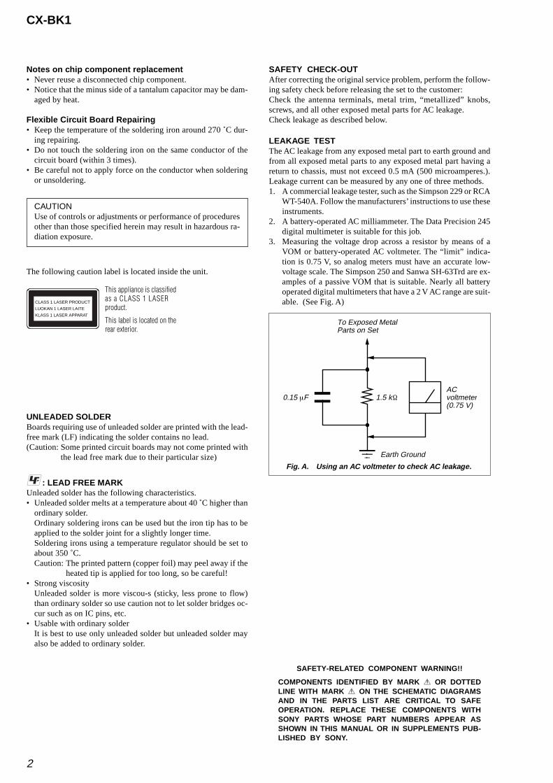
SAFETY CHECK-OUTAfter correcting the original service problem, perform the follow-ing safety check before releasing the set to the customer:Check the antenna terminals, metal trim, “metallized” knobs,screws, and all other exposed metal parts for AC leakage.Check leakage as described below.
LEAKAGE TESTThe AC leakage from any exposed metal part to earth ground andfrom all exposed metal parts to any exposed metal part having areturn to chassis, must not exceed 0.5 mA (500 microamperes.).Leakage current can be measured by any one of three methods.1. A commercial leakage tester, such as the Simpson 229 or RCA
WT-540A. Follow the manufacturers’ instructions to use theseinstruments.
2. A battery-operated AC milliammeter. The Data Precision 245digital multimeter is suitable for this job.
3. Measuring the voltage drop across a resistor by means of aVOM or battery-operated AC voltmeter. The “limit” indica-tion is 0.75 V, so analog meters must have an accurate low-voltage scale. The Simpson 250 and Sanwa SH-63Trd are ex-amples of a passive VOM that is suitable. Nearly all batteryoperated digital multimeters that have a 2 V AC range are suit-able. (See Fig. A)
Fig. A. Using an AC voltmeter to check AC leakage.
1.5 kΩ0.15 µFACvoltmeter(0.75 V)
To Exposed MetalParts on Set
Earth Ground
UNLEADED SOLDERBoards requiring use of unleaded solder are printed with the lead-free mark (LF) indicating the solder contains no lead.(Caution: Some printed circuit boards may not come printed with
the lead free mark due to their particular size)
: LEAD FREE MARKUnleaded solder has the following characteristics.• Unleaded solder melts at a temperature about 40 ˚C higher than
ordinary solder.Ordinary soldering irons can be used but the iron tip has to beapplied to the solder joint for a slightly longer time.Soldering irons using a temperature regulator should be set toabout 350 ˚C.Caution: The printed pattern (copper foil) may peel away if the
heated tip is applied for too long, so be careful!• Strong viscosity
Unleaded solder is more viscou-s (sticky, less prone to flow)than ordinary solder so use caution not to let solder bridges oc-cur such as on IC pins, etc.
• Usable with ordinary solderIt is best to use only unleaded solder but unleaded solder mayalso be added to ordinary solder.
CLASS 1 LASER PRODUCT
LUOKAN 1 LASER LAITE
KLASS 1 LASER APPARAT
This appliance is classifiedas a CLASS 1 LASERproduct.
This label is located on therear exterior.

CX-BK1
3
TABLE OF CONTENTS
1. SERVICING NOTES ................................................ 4
2. GENERALLocation of Controls ....................................................... 6
3. DISASSEMBLY3-1. Disassembly Flow ........................................................... 83-2. Panel ................................................................................ 93-3. Top Panel Block .............................................................. 93-4. Front Panel Assy ............................................................. 103-5. MAIN Board ................................................................... 103-6. Rear Cover ....................................................................... 113-7. Tuner (FM/AM) .............................................................. 113-8. SPEAKER Board ............................................................ 123-9. ACDC Board, Power Transformer .................................. 123-10. AMP Board ..................................................................... 133-11. CD Mechanism Deck (CDM69BV-30CBD64NS) ......... 133-12. Signal Cassette Mechanism ............................................ 143-13. Base Unit Section ............................................................ 143-14. Base Unit (BU-30CBD64NS) ......................................... 153-15. BD Board ......................................................................... 153-16. SW (1) Board, SW (2) Board, SW (3) Board,
SW (4) Board, Bracket (Top) Assy ................................. 163-17. CONNECTOR Board ..................................................... 163-18. Motor (Stocker) Assy (Stocker) (M761) ........................ 173-19. Motor (Roller) Assy (Roller) (M781) ............................. 173-20. Motor (Mode) Assy (Mode) (M771) .............................. 183-21. Rubber Roller (Slider) Assy ........................................... 183-22. Timing Belt (Front/Rear) ................................................ 193-23. Cam (Gear) ...................................................................... 193-24. SENSOR Board ............................................................... 20
4. ASSEMBLY4-1. How to Install the Cam (Eject Lock) .............................. 214-2. How to Install the Cam (Gear) ........................................ 214-3. How to Install the Gear (Mode C) .................................. 224-4. How to Install the Gear (Mode Cam) ............................. 224-5. How to Install the Rotary Encoder (S702),
Gear (Stocker Communication) ...................................... 234-6. How to Install the Stocker Assy ...................................... 23
5. TEST MODE .............................................................. 24
6. MECHANICAL ADJUSTMENTS ....................... 25
7. ELECTRICAL ADJUSTMENTSDeck Section ................................................................... 25CD Section ...................................................................... 28
8. DIAGRAMS8-1. Block Diagram – CD Section – ..................................... 318-2. Block Diagram – TUNER/TAPE/USB Section – ......... 328-3. Block Diagram – AMP Section – .................................. 338-4. Block Diagram – POWER SUPPLY Section – ............. 348-5. Note for Printed Wiring Boards
and Schematic Diagrams ................................................ 358-6. Printed Wiring Board – BD Board – ............................. 368-7. Schematic Diagram – BD Board – ................................ 378-8. Printed Wiring Boards – CHANGER Section – ............ 388-9. Schematic Diagram – CHANGER Section – ................ 398-10. Printed Wiring Board
– DECK Board (Except US model) – ............................ 408-11. Schematic Diagram
– DECK Board (Except US model) – ............................. 41
8-12. Printed Wiring Board – MAIN Board – ........................ 438-13. Schematic Diagram – MAIN Board (1/4) – .................. 448-14. Schematic Diagram – MAIN Board (2/4) – .................. 458-15. Schematic Diagram – MAIN Board (3/4) – .................. 468-16. Schematic Diagram – MAIN Board (4/4) – .................. 478-17. Printed Wiring Board – USB AUX Board – .................. 488-18. Schematic Diagram – USB AUX Board – ..................... 498-19. Printed Wiring Boars – MIC Board
(Chilean, Peruvian and Mexican models) – ................... 508-20. Schematic Diagram – MIC Board
(Chilean, Peruvian and Mexican models) – ................... 518-21. Schematic Diagram – AMP Board (1/2) – .................... 528-22. Schematic Diagram – AMP Board (2/2) – .................... 538-23. Printed Wiring Board – AMP Board – .......................... 548-24. Printed Wiring Board – HEADPHONE Board – .......... 558-25. Schematic Diagram – HEADPHONE Board – ............. 558-26. Printed Wiring Board – SPEAKER Board – ................. 568-27. Schematic Diagram – SPEAKER Board – .................... 578-28. Printed Wiring Boards – KEY Section – ....................... 588-29. Schematic Diagram – KEY Section – ........................... 598-30. Printed Wiring Boards – LCD Section – ....................... 608-31. Schematic Diagram – LCD Section – ........................... 618-32. Printed Wiring Board – ACDC Board – ........................ 628-33. Schematic Diagram – ACDC Board – ........................... 638-34. Printed Wiring Board
– PT Board (US, AEP and UK models) – ...................... 648-35. Schematic Diagram
– PT Board (US, AEP and UK models) – ...................... 658-36. Printed Wiring Board – PT Board
(Chilean, Peruvian and Mexican models) – ................... 668-37. Schematic Diagram – PT Board
(Chilean, Peruvian and Mexican models) – ................... 678-38. IC Pin Function Description ........................................... 73
9. EXPLODED VIEWS9-1. Panel Section ................................................................... 799-2. Top Panel Block .............................................................. 809-3. Front Panel Block-1 ........................................................ 819-4. Front Panel Block-2 ........................................................ 829-5. Front Panel Block-3 ........................................................ 839-6. Chassis Block-1 ............................................................... 849-7. Chassis Block-2 ............................................................... 859-8. CD Mechanism Deck Section-1
(CDM69BV-30CBD64NS) ............................................. 869-9. CD Mechanism Deck Section-2
(CDM69BV-30CBD64NS) ............................................. 879-10. CD Mechanism Deck Section-3
(CDM69BV-30CBD64NS) ............................................. 889-11. CD Mechanism Deck Section-4
(CDM69BV-30CBD64NS) ............................................. 899-12. CD Mechanism Deck Section-5
(CDM69BV-30CBD64NS) ............................................. 909-13. CD Mechanism Deck Section-6
(CDM69BV-30CBD64NS) ............................................. 919-14. Optical Pick-up Section (BU-30CBD64NS) .................. 92
10. ELECTRICAL PARTS LIST ............................... 93
4
CX-BK1SECTION 1
SERVICING NOTES
NOTES ON HANDLING THE OPTICAL PICK-UPBLOCK OR BASE UNIT
The laser diode in the optical pick-up block may suffer electro-static break-down because of the potential difference generatedby the charged electrostatic load, etc. on clothing and the humanbody.During repair, pay attention to electrostatic break-down and alsouse the procedure in the printed matter which is included in therepair parts.The flexible board is easily damaged and should be handled withcare.
NOTES ON LASER DIODE EMISSION CHECKThe laser beam on this model is concentrated so as to be focusedon the disc reflective surface by the objective lens in the opticalpick-up block. Therefore, when checking the laser diode emis-sion, observe from more than 30 cm away from the objective lens.
LASER DIODE AND FOCUS SEARCH OPERATIONCHECKCarry out the “S curve check” in “CD section adjustment” andcheck that the S curve waveforms is output three times.
• MODEL IDENTIFICATION– Rear Cover –
MODEL PART No.
US model 4-245-039-0[]
Chilean and Peruvian models 4-245-039-1[]
AEP and UK models 4-245-039-2[]
Mexican model 4-245-039-3[]
PART No.
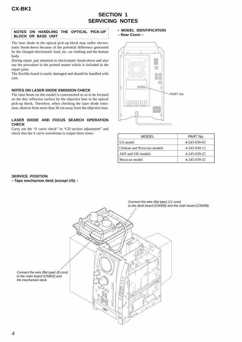
SERVICE POSITION– Tape mechanism deck (except US) –
Connect the wire (flat type) (8 core)to the main board (CN903) and the mechanism deck.
Connect the wire (flat type) (11 core)to the deck board (CN008) and the main board (CN009).

5
CX-BK1
– CD mechanism deck –• In checking the CD mechanism deck section, prepare three extension jigs (Part No. J-2501-242-A:1.00 mm 11core/
Part No. J-2501-245-A: 1.00 mm 23 core/Part No. J-2501-248-A: 1.00mm 27 core).
Note: The CD mechanism deck of this model is a vertical type and putting it vertically as shown in the figure is the standard position.When checking signals such as RF waveforms, operate it with the CD mechanism deck in the standard position as shown below.
– main board, ACDC board –• For connecting the CD mechanism deck, prepare three extension jigs. (Refer to “– CD mechanism deck –”)
Connect the extension jig (J-2501-248-A) to the connector board (CN701) andthe main board (CN901).
Connect the extension jig (J-2501-242-A) to the BD board (CN104) and the main board (CN507).
Connect the extension jig (J-2501-245-A) to the BD board (CN102) andthe main board (CN902).
AMP board
speaker board
PT board
ACDC board
CD mechanism deck
tuner unit
main board
front panel section

6
CX-BK1
Main unit: front
1 POWER 6STANDBY/ONSwitches the unit on and off (standby).
2 FUNCTION Switches the active function among CD, USB, TAPE (Except US model), TUNER, VIDEO and AUX.
3 BANDSelect tuner function and the tuner band.
4 GEQSelects a sound equalization curve.
i-BassProduces rich and clear low frequency sound.
5 TREBLE/MIDDLEAdjusts the treble or middle range level.
BASSAdjusts the bass level.
6 PLA Y MODE (US model)Selects various CD play mode.
7 TUNING DOWNf/r, UPg/tCD: skips to a previous or a succeeding track whenpressed, searches a track in fast forward or reverseplayback when held down.
#When the unit is turned off: activates or deactivatedDEMO.Changes the display in MP3-CD or USB source.
DISPLAYChanges the display in CD playback mode.Turns the back light on and off when the unit is turnedoff.
MODESelects various modes (sound adjustment, etc.) whenused in combination with ENTER and MULTI JOG.Switches the ECO mode on and off when the unit is turnedoff.
$ aPAUSE/SETPauses CD play.
sSTOP/CLEARStops CD play.
cPRESET (US model)Starts CD play.
% MULTI JOGWhen used in combination with ENTER and MULTI JOG,CD: selects a track.Tuner: selects a preset station.
^ ENTERFixes the modes and the time (clock and timer, etc.) whenused in combination with ENTER and MULTI JOG.
& PHONES jackPlug in optional headphones set with a stereo mini plug(Ø3.5 mm). Speaker output is canceled.
3
0!
4
9
@
#
)
6
%
$
^
&
*(
21
8
7
5
wREC (Except US model)Starts tape recording.Also used to enter 4-second blank spaces duringrecording.
Tape: rewinds or fast forwards the tape. (Except US
Tuner: manually tunes up or down within the band.
8 USB terminalAccepts sound signals from a personal computer.Connect your personal computer to this terminal with aUSB cable so that the unit can output the sound of anaudio file which is played back by the Winamp3 on yourcomputer.Be sure to see “CONNECTING A PERSONALCOMPUTER” for the details about the computerrequirements, how to connect and so on before actuallyconnecting your computer.
9 LINE IN (VIDEO/AUDIO) jacksAccepts analog signals from external equipment.Connect using an optional connecting cable with RCAphono plugs (red plug to R jack, white plug to L jack,yellow plug to VIDEO jack).Refer also to the operating instructions of your equipment.To switch function to external input, press FUNCTIONrepeatedly to display “VIDEO”.
0 zEJECTEjects the disc(s).
! DISC SELECT (1-5)Selects a disc slot.Starts CD play for one desired disc.
@ VOLUME Adjusts the volume.
model)
dPRESET (Except US model)Starts CD or tape play.
* MIC MIXING (Chilean and Peruvian
) ALBUM/PLAY LIST k,iSkips to a previous or succeeding album or play list.
models)Adjusts the microphone volume.
( MIC jack (Chilean and Peruvian models)Connects the microphone.
TITLE
SECTION 2GENERAL
This section is extracted frominstruction manual.
• LOCATION OF CONTROLS
Main unit: rear
1
4
2
3
5
6
1 AM LOOP jack and FM 75 Ω terminalPlug in the supplied AM and FM antennas.
2 AUX IN jacksAccept analogue sound signals from external equipment.Connect external equipment using an optional connectingcable with RCA phono plugs (red plug to R jack, whiteplug to L jack). Refer also to the operating instructionsfor your equipment.To switch function to external input, press FUNCTIONrepeatedly to display “AUX” (US model) or “MD”(Chilean, Peruvian and Mexican models).
3 AUX OUT jacksAnalog sound signals for all functions can be outputthrough these jacks. Use a cable with RCA phono plugsto connect audio equipment.Connect the red plug to the R jack, and the white plug tothe L jack.However, the signal is not output when the function is“VIDEO” or “AUX” (US model) or “MD” (Chilean,Peruvian and Mexican models).
4 VIDEO OUTSignals from VIDEO IN jack output through this jack.
5 #SPEAKERS terminalsConnect the speaker cords of the supplied speakers.
6 AC power cord
7
CX-BK1
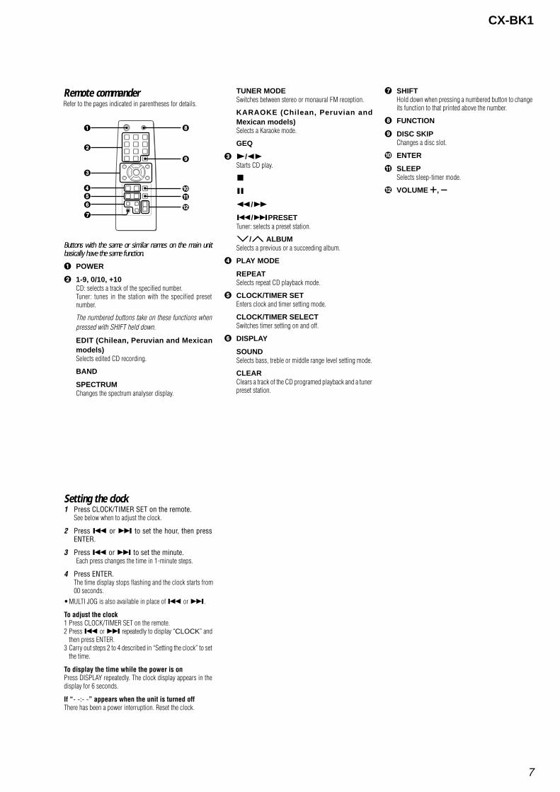
Remote commanderRefer to the pages indicated in parentheses for details.
1
4
6
7
9
8
0!
@
5
3
2
Buttons with the same or similar names on the main unitbasically have the same function.
1 POWER
2 1-9, 0/10, +10CD: selects a track of the specified number.Tuner: tunes in the station with the specified presetnumber.
The numbered buttons take on these functions whenpressed with SHIFT held down.
3 c/dStarts CD play.
s
a
f/g
r/ tPRESET Tuner: selects a preset station.
M/ N ALBUMSelects a previous or a succeeding album.
4 PLAY MODE
REPEATSelects repeat CD playback mode.
5 CLOCK/TIMER SET Enters clock and timer setting mode.
CLOCK/TIMER SELECTSwitches timer setting on and off.
6 DISPLAY
SOUNDSelects bass, treble or middle range level setting mode.
CLEARClears a track of the CD programed playback and a tunerpreset station.
7 SHIFTHold down when pressing a numbered button to changeits function to that printed above the number.
8 FUNCTION
9 DISC SKIPChanges a disc slot.
0 ENTER
! SLEEPSelects sleep-timer mode.
@ VOLUME +, -
EDIT (Chilean, Peruvian and Mexican
BAND
SPECTRUMChanges the spectrum analyser display.
TUNER MODESwitches between stereo or monaural FM reception.
models)Selects edited CD recording.
KARAOKE (Chilean, Peruvian and
GEQ
Mexican models)Selects a Karaoke mode.
Setting the clock1 Press CLOCK/TIMER SET on the remote.
See below when to adjust the clock.
2 Press r or t to set the hour, then pressENTER.
3 Press r or t to set the minute.Each press changes the time in 1-minute steps.
4 Press ENTER.The time display stops flashing and the clock starts from00 seconds.
•MULTI JOG is also available in place of r or t.
To adjust the clock1 Press CLOCK/TIMER SET on the remote.2 Press r or t repeatedly to display “CLOCK” and
then press ENTER.3 Carry out steps 2 to 4 described in “Setting the clock” to set
the time.
To display the time while the power is onPress DISPLAY repeatedly. The clock display appears in thedisplay for 6 seconds.
If “- -:- -” appears when the unit is turned offThere has been a power interruption. Reset the clock.
CX-BK1
8
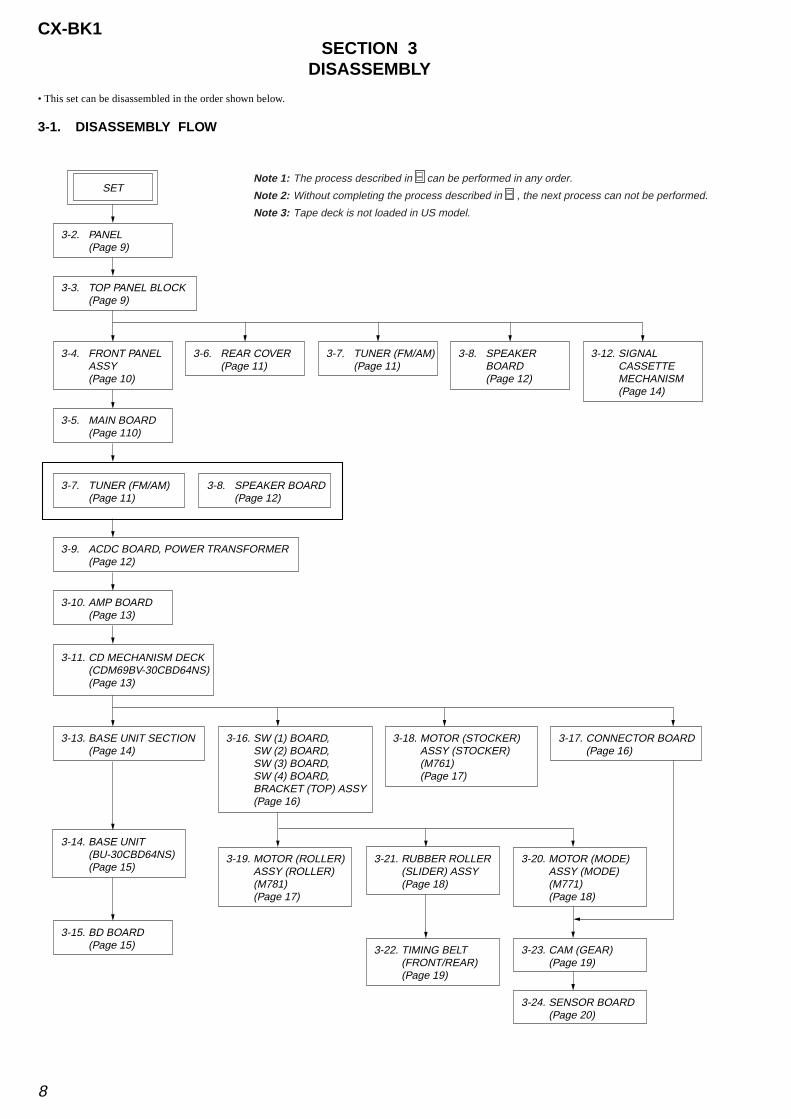
• This set can be disassembled in the order shown below.
3-1. DISASSEMBLY FLOW
SECTION 3DISASSEMBLY
3-2. PANEL(Page 9)
3-5. MAIN BOARD(Page 110)
3-15. BD BOARD(Page 15) 3-22. TIMING BELT
(FRONT/REAR)(Page 19)
3-23. CAM (GEAR)(Page 19)
3-24. SENSOR BOARD(Page 20)
3-10. AMP BOARD(Page 13)
3-11. CD MECHANISM DECK(CDM69BV-30CBD64NS)(Page 13)
3-13. BASE UNIT SECTION(Page 14)
3-16. SW (1) BOARD,SW (2) BOARD,SW (3) BOARD,SW (4) BOARD,BRACKET (TOP) ASSY(Page 16)
3-18. MOTOR (STOCKER) ASSY (STOCKER) (M761)(Page 17)
3-17. CONNECTOR BOARD(Page 16)
3-14. BASE UNIT(BU-30CBD64NS)(Page 15)
3-19. MOTOR (ROLLER) ASSY (ROLLER) (M781)(Page 17)
3-21. RUBBER ROLLER (SLIDER) ASSY(Page 18)
3-20. MOTOR (MODE) ASSY (MODE) (M771)(Page 18)
3-7. TUNER (FM/AM)(Page 11)
3-8. SPEAKER BOARD(Page 12)
3-4. FRONT PANEL ASSY(Page 10)
3-6. REAR COVER(Page 11)
3-7. TUNER (FM/AM)(Page 11)
3-8. SPEAKER BOARD(Page 12)
3-12. SIGNAL CASSETTEMECHANISM(Page 14)
3-3. TOP PANEL BLOCK(Page 9)
3-9. ACDC BOARD, POWER TRANSFORMER(Page 12)
SETNote 1: The process described in can be performed in any order.
Note 2: Without completing the process described in , the next process can not be performed.
Note 3: Tape deck is not loaded in US model.
CX-BK1
9
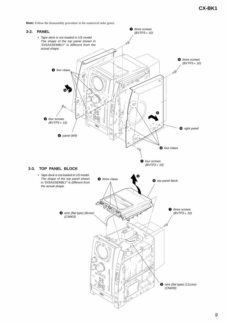
Note: Follow the disassembly procedure in the numerical order given.
3-2. PANEL
3-3. TOP PANEL BLOCK
1 three screws(BVTP3 × 10)
6 three screws(BVTP3 × 10)
7 four screws(BVTP3 × 10)
2 four screws(BVTP3 × 10)
5 panel (left)
3 four claws
8 four claws
4
9
0 right panel
1 three screws(BVTP3 × 10)
2 three claws
4 wire (flat type) (8core)(CN903)
3
6 top panel block
5 wire (flat type) (11core)(CN009)
• Tape deck is not loaded in US model.The shape of the top panel shown in“DISASSEMBLY” is different from theactual shape.
• Tape deck is not loaded in US model.The shape of the top panel shownin “DISASSEMBLY” is different fromthe actual shape.

CX-BK1
10
3 two screws(BVTP3 × 10)
4 screw(BVTP3 × 10)
qa two screws(BVTP3 × 6)
9 wire (flat type) (23core)(CN902)
2 wire (flat type)(11core: US, E51) (CN509)/(15core: AEP, UK) (CN508)
1 wire (flat type) (11core)(CN502)
6 wire (flat type) (11core)(CN507)
7 connector(CN007)
8 connector(CN006)
qs main board
5
0 wire (flat type) (27core)(CN901)
1 wire (flat type) (19core)(CN905)
9 front panel assy
6 two screws(BVTP3 × 10)
5 five screws(BVTP3 × 10) 7 six screws
(BVTP3 × 10)
4 connector (CN530)
8 two claws
2 wire (flat type) (17core)(CN004)
3 wire (flat type) (5core)(CN504)
E51, MX3-4. FRONT PANEL ASSY
3-5. MAIN BOARD
CX-BK1
11
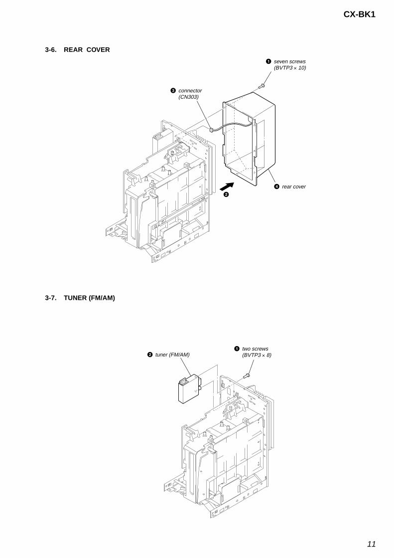
3-6. REAR COVER
3-7. TUNER (FM/AM)
1 seven screws(BVTP3 × 10)
2
4 rear cover
3 connector(CN303)
1 two screws(BVTP3 × 8)2 tuner (FM/AM)
CX-BK1
12
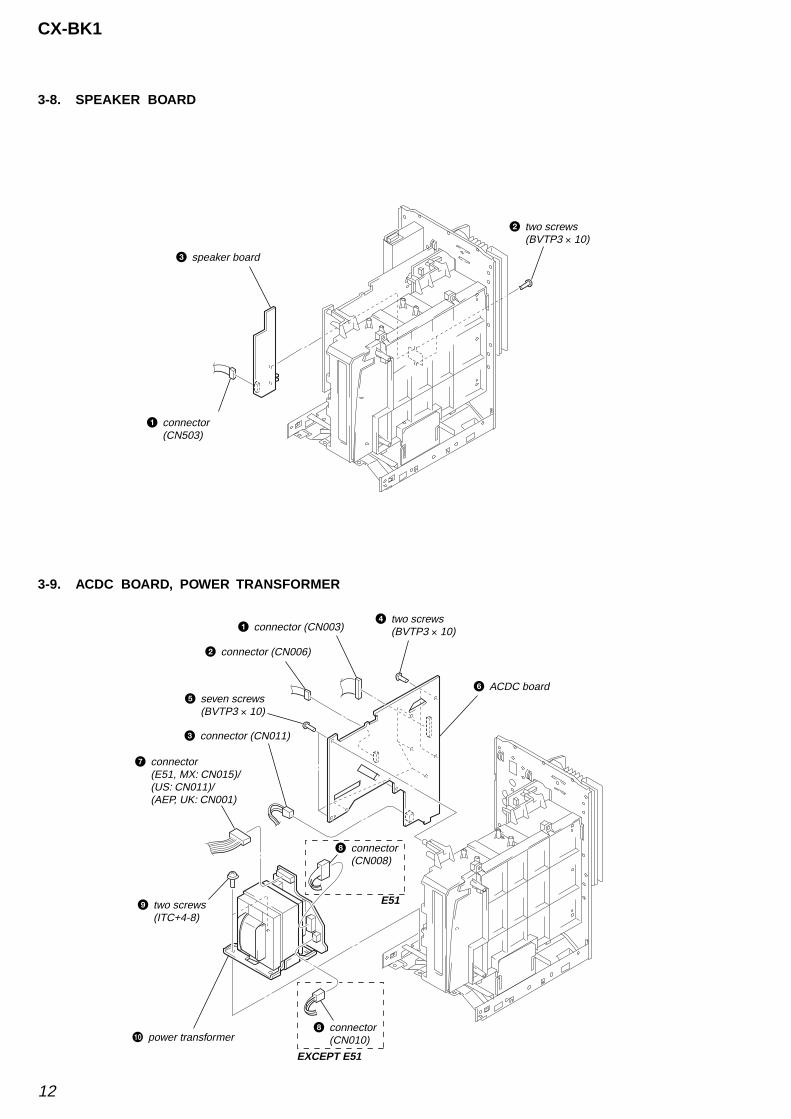
2 two screws(BVTP3 × 10)
1 connector(CN503)
3 speaker board
3-8. SPEAKER BOARD
3-9. ACDC BOARD, POWER TRANSFORMER
4 two screws(BVTP3 × 10)
5 seven screws(BVTP3 × 10)
9 two screws(ITC+4-8)
0 power transformer8 connector
(CN010)
8 connector(CN008)
E51
EXCEPT E51
7 connector(E51, MX: CN015)/(US: CN011)/(AEP, UK: CN001)
3 connector (CN011)
2 connector (CN006)
1 connector (CN003)
6 ACDC board

CX-BK1
13
3-10. AMP BOARD
3-11. CD MECHANISM DECK (CDM69BV-30CBD64NS)
3 two screws(BVTP3 × 10)
4 two screws(BVTP3 × 10)
1 two screws(BVTP3 × 10)
2 CD support board
5 AMP board
1 four screws(BVTP3 × 10)
2 four screws(BVTP3 × 10)
3 disk mechanical cover
4 four screws(BVTP3 × 10)
5 disk mecanical holder
6 CD mechanism deck(CDM69BV-30CBD64NS)

CX-BK1
14
3-12. SIGNAL CASSETTE MECHANISM
1 connector(CN302)
2 four screws(BVTP3 × 10)
3 signal cassette mechanism
3-13. BASE UNIT SECTION
4 boss
6 boss
3 boss
5 boss
1 floating screw (DIA. 12)
2 screw (+PTPWH) (M2) (DIA. 7)
7 base unit section
• Tape deck is not loaded in US model.
CX-BK1
15
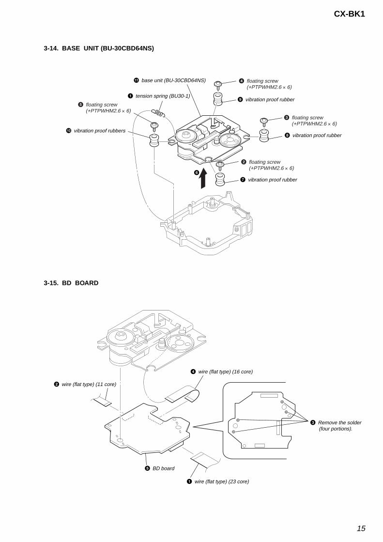
3-14. BASE UNIT (BU-30CBD64NS)
3-15. BD BOARD
1 tension spring (BU30-1)
qa base unit (BU-30CBD64NS)
8 vibration proof rubber
3 floating screw(+PTPWHM2.6 × 6)
5 floating screw(+PTPWHM2.6 × 6)
4 floating screw(+PTPWHM2.6 × 6)
2 floating screw(+PTPWHM2.6 × 6)
9 vibration proof rubber
q; vibration proof rubbers
7 vibration proof rubber6
3 Remove the solder (four portions).
5 BD board
4 wire (flat type) (16 core)
1 wire (flat type) (23 core)
2 wire (flat type) (11 core)
CX-BK1
16
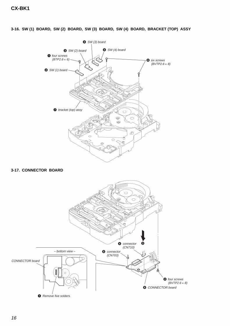
3-16. SW (1) BOARD, SW (2) BOARD, SW (3) BOARD, SW (4) BOARD, BRACKET (TOP) ASSY
6 six screws (BVTP2.6 × 8)
5 SW (4) board
4 SW (3) board
3 SW (2) board
2 SW (1) board
7 bracket (top) assy
1 four screws (BTP2.6 × 6)
3
1 Remove five solders.
– bottom view –
CONNECTOR board
2 four screws (BVTP2.6 × 8)
4 connector(CN710)
5 connector(CN703)
6 CONNECTOR board
3-17. CONNECTOR BOARD
CX-BK1
17
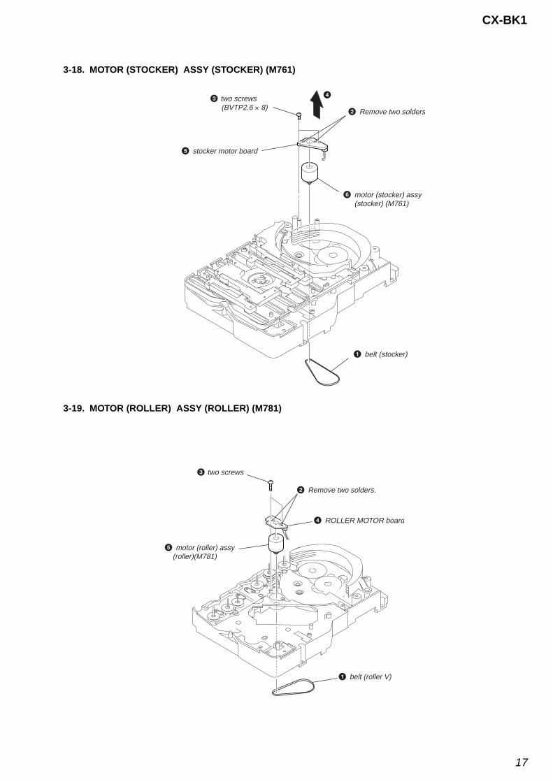
3-18. MOTOR (STOCKER) ASSY (STOCKER) (M761)
4
5 stocker motor board
3 two screws (BVTP2.6 × 8)
2 Remove two solders
6 motor (stocker) assy(stocker) (M761)
1 belt (stocker)
1 belt (roller V)
4 ROLLER MOTOR board
2 Remove two solders.
3 two screws
5 motor (roller) assy (roller)(M781)
3-19. MOTOR (ROLLER) ASSY (ROLLER) (M781)
CX-BK1
18
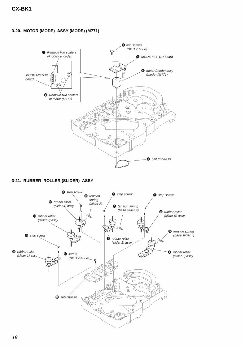
3-20. MOTOR (MODE) ASSY (MODE) (M771)
3-21. RUBBER ROLLER (SLIDER) ASSY
1 Remove five soldersof rotary encoder.
2 Remove two soldersof motor (M771)
MODE MOTORboard
3 two screws (BVTP2.6 × 8)
4 MODE MOTOR board
5 belt (mode V)
6 motor (mode) assy(mode) (M771)
qg sub chassis
qf screw(BVTP2.6 × 8)
8 step screw
qs step screw
5 step screw9 tension
spring(slider 2)
6 tension spring(base slider 4)
0 rubber roller(slider 4) assy
7 rubber roller(slider 1) assy
qa rubber roller(slider 2) assy
qd rubber roller(slider 1) assy
3 tension spring(base slider 5)
1 step screw
4 rubber roller(slider 5) assy
2 rubber roller(slider S) assy

CX-BK1
19
3-22. TIMING BELT (FRONT/REAR)
3-23. CAM (GEAR)
Note: Refer to assembly (Section 4)
2 gear (mode cam): Note
1 screw(PTPWH2.6 × 8)
3 slider (mode cam) assy
5 two gears(center)
7 two gears (center)
8 timing belt (rear)
9 timing belt (rear)
4 gear(timing)
6 timing belt(front)
timing belt (rear)
When install three timing belts, its pass under each claws.
timing belt (rear)
timing belt (front)
claw
claw
claw
claw
qf cam (gear): Note
qs gear(mode cam)
0 gear (mode C):Note
4 gear (mode 5)
8 gear (mode D)
6 gear (mode 5)
1 screw(PTPWH2.6 × 8)
7 screw (PTPWH2.6 × 8)
9 screw (PTPWH2.6 × 8)
qa screw (PTPWH2.6 × 8)
3 screw (PTPWH2.6 × 8)
5 screw (PTPWH2.6 × 8)
2 pulley(mode deceleration)
qd screw
Note: Refer to assembly (Section 4).
CX-BK1
20
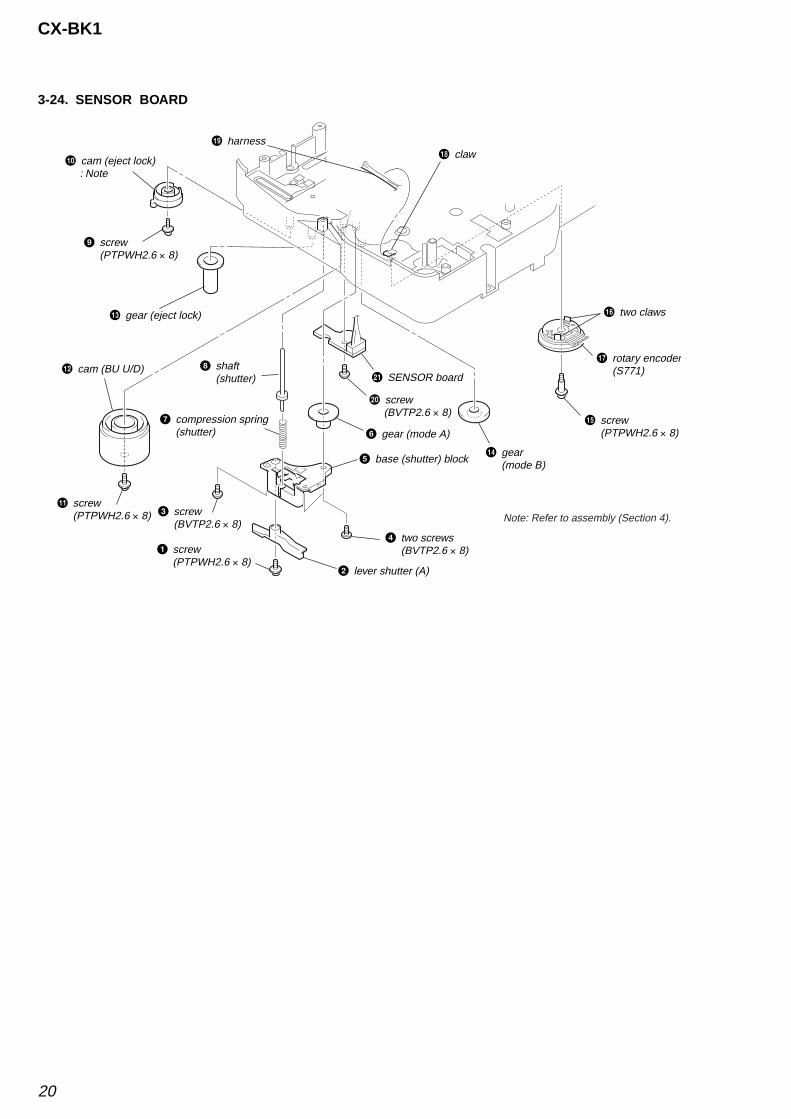
3-24. SENSOR BOARD
ql harness
qd gear (eject lock)
q; cam (eject lock) : Note
qh two claws
qj rotary encoder(S771)
qf gear (mode B)
w; screw (BVTP2.6 × 8)
qg screw (PTPWH2.6 × 8)
wa SENSOR board8 shaft
(shutter)
7 compression spring (shutter)
qs cam (BU U/D)
qa screw (PTPWH2.6 × 8) 3 screw
(BVTP2.6 × 8)
1 screw (PTPWH2.6 × 8)
4 two screws (BVTP2.6 × 8)
2 lever shutter (A)
5 base (shutter) block
6 gear (mode A)
9 screw (PTPWH2.6 × 8)
qk claw
Note: Refer to assembly (Section 4).

CX-BK1
21
SECTION 4ASSEMBLY
• This set can be assembled in the order shown below.
4-1. HOW TO INSTALL THE CAM (EJECT LOCK)
4-2. HOW TO INSTALL THE CAM (GEAR)
mark
cam (BU U/D)
cam (eject lock)
– bottom view • front –
gear (eject lock)
1 Rotate the cam (BU U/D) fully in the direction of arrow.
2 Engage the gear (eject lock) and the gear of the cam (eject lock)aligning the mark with the center of the gear (eject lock).
bosscam (gear)
mark
cam (BU U/D)
– bottom view • front –
1 Check that the cam (BU U/D) can not be rotated in the direction of arrow.
2 Align the mark on the cam (gear) with the boss as shown in the figureand install the cam (gear).
CX-BK1
22
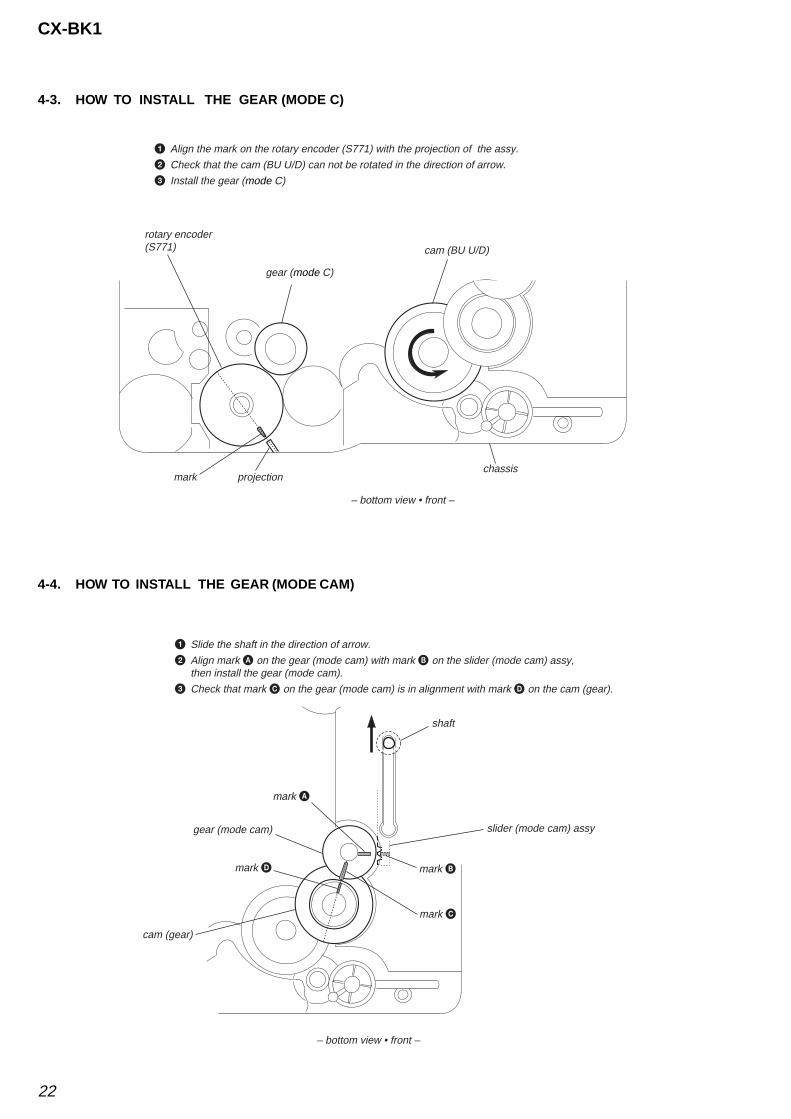
4-3. HOW TO INSTALL THE GEAR (MODE C)
1 Align the mark on the rotary encoder (S771) with the projection of the assy.
2 Check that the cam (BU U/D) can not be rotated in the direction of arrow.
3 Install the gear (mode C)
– bottom view • front –
gear (mode C)
rotary encoder(S771) cam (BU U/D)
mark projectionchassis
mark B
slider (mode cam) assy
shaft
mark A
mark D
gear (mode cam)
cam (gear)
mark C
1 Slide the shaft in the direction of arrow.
2 Align mark A on the gear (mode cam) with mark B on the slider (mode cam) assy, then install the gear (mode cam).
3 Check that mark C on the gear (mode cam) is in alignment with mark D on the cam (gear).
– bottom view • front –
4-4. HOW TO INSTALL THE GEAR (MODE CAM)
CX-BK1
23
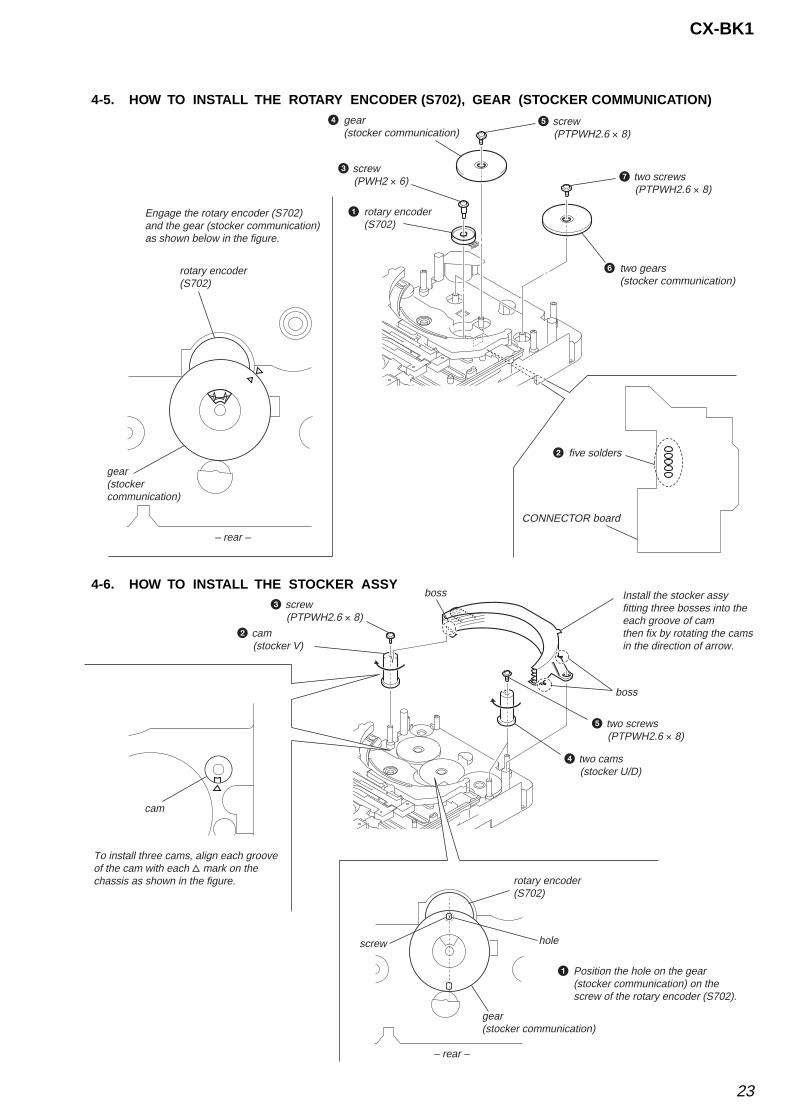
4-5. HOW TO INSTALL THE ROTARY ENCODER (S702), GEAR (STOCKER COMMUNICATION)
4-6. HOW TO INSTALL THE STOCKER ASSY
2 five solders
6 two gears(stocker communication)
4 gear(stocker communication)
CONNECTOR board
7 two screws (PTPWH2.6 × 8)
5 screw (PTPWH2.6 × 8)
3 screw (PWH2 × 6)
rotary encoder(S702)
gear(stocker communication)
– rear –
1 rotary encoder(S702)
Engage the rotary encoder (S702)and the gear (stocker communication)as shown below in the figure.
2 cam (stocker V)
3 screw (PTPWH2.6 × 8)
4 two cams (stocker U/D)
5 two screws (PTPWH2.6 × 8)
boss
boss
rotary encoder(S702)
Install the stocker assy fitting three bosses into the each groove of cam then fix by rotating the cams in the direction of arrow.
hole
gear(stocker communication)
– rear –
screw
1 Position the hole on the gear (stocker communication) on thescrew of the rotary encoder (S702).
To install three cams, align each grooveof the cam with each f mark on the chassis as shown in the figure.
cam
24
CX-BK1
[Cold Reset]* The cold reset clears all data including preset data stored in
the RAM to initial conditions. Execute this mode when re-turning the set to the customer.
Procedure:1. Press the POWER 1 button to turn off the main power.2. While depressing the x button, press the POWER 1 button.3. The fluorescent indicator tube does not display any message
and the set is reset.
[Version Display Mode]* The version of the microcomputer is displayed.Procedure:1. Press the POWER 1 button to turn the set on.2. To enter the test mode, press two buttons x and POWER 1
simultaneously for more than five seconds. The version of themicrocomputer is displayed.
[FL Tube Check]* All fluorecent segments are tested.Procedure:1. Insert a disc, and extract an AC plug.2. While depressing the [FUNCTION] button, insert an AC plug
to enter the test mode.3. The message “CD TEST” is displayed, the initialization is
performed.Then all segments of the fluorecent indicator tube are turned on.
[CD Ship Mode]* This mode moves the optical pick-up to the position durable
to vibration. Use this mode when returning the set to the cus-tomer after repair.
Procedure:1. Press the POWER 1 button to turn the set on.2. Set the FUNCTION to CD.3. Press the x button for more than five seconds.4. After a message “MECHA LOCK” is displayed on the fluo-
rescent indicator tube, the CD ship mode is set and the poweris turned off.
[Disc Tray Lock]The disc tray lock function for the antitheft of an demonstrationdisc in the store is equipped.Setting Procedure :1. Press the POWER 1 button to turn the set on.2. Press two buttons of x and Z simultaneously for five sec-
onds.3. The message “LOCKED” is displayed and the tray is locked.Releasing Procedure :1. Press two buttons of x and Z simultaneously for five sec-
onds again.2. The message “UNLOCKED” is displayed and the tray is un-
locked.Note : When “LOCKED” is displayed, the tray lock is not releasedby turning power on/off with the POWER 1 button.
[AMP Test]* This mode is used to check the function of the amplifier.Procedure:1. Extract an AC plug.2. While depressing the [GEQ] button, insert an AC plug to en-
ter the AMP test mode. The message “AMP TEST” is displayed.3. The message “Volume MAX” is displayed, when the [VOL-UME] knob is rotated clockwise. The message “Volume 0” isdisplayed, when the [VOLUME] knob is rotated counterclock-wise.
4. Each time the [BASE] or [TREBLE] knob is turned, the mes-
sage “EQ MAX”, “EQ MIN” or “EQ FLAT” is displayed inthis order.
[AM Channel Step 9 kHz/10kHz Selection Mode]* Either the 9 kHz step or 10 kHz step can be selected for the
AM channel step.Procedure:1. Set the FUNCTION to AM.2. While depressing the [BAND] button, press the POWER 1 but-
ton.3. The channel step is changed over.
[CD Test Mode]* This mode can run the CD sled motor freely. Use this mode,
for instance, when cleaning the pickup.Procedure:1. Extract an AC plug.2. While depressing the [FUNCTION] button, insert an AC plug
to enter the CD test mode. The message “CD TEST” is dis-played.
3. With the CD in stop status, press the > button to move thepickup to outside track, or press the . button to inside track.
4. When press the B button, normal playback is performed.5. Each time the B button is pressed during normal playback,
the tracking servo is switched on or off.
[CD Repeat 5 Times Limit Release Mode]Procedure:1. Press the POWER 1 button to turn the set on.2. Select the FUNCTION to CD.3. Press three buttons of x and [FUNCTION] and B simulta-
neously.4. The repeat all mark blinks and then repeat 5 times limit is
released.
SECTION 5TEST MODE
25
CX-BK1SECTION 6
MECHANICAL ADJUSTMENTS
• TAPE MECHANISM DECK SECTION
Note: Tape deck is not loaded in US model.
Precaution1. Clean the following parts with a denatured alcohol-moistened
swab:record/playback heads pinch rollerserase head rubber beltscapstan idlers
2. Demagnetize the record/playback head with a headdemagnetizer.
3. Do not use a magnetized screwdriver for the adjustments.4. After the adjustments, apply suitable locking compound to the
parts adjusted.5. The adjustments should be performed with the rated power
supply voltage unless otherwise noted.
Torque Measurement
2.94 – 7.84 mN • m(30 to 79 g • cm)
(0.42 – 1.11 oz • inch)
0.15 – 0.6 mN • m2 to 6 g • cm
(0.03 – 0.08 oz • inch)
2.94 – 7.84 mN • m(30 to 79 g • cm)
(0.42 – 1.11 oz • inch)
2.94 – 7.84 mN • m(30 to 79 g • cm)
(0.42 – 1.11 oz • inch)
6.86 – 17.64 mN • m(70 to 179 g • cm)
(0.98 – 2.49 oz • inch)
9.8 mN • m(100 • cm or more)
(1.4 oz • inch or more)
9.8 mN • m(100 • cm or more)
(1.4 oz • inch or more)
Mode Torque meter
CQ-102C
CQ-102C
CQ-102RC
CQ-102RC
CQ-201B
CQ-403A
CQ-403R
Meter reading
FWD
FWDback tension
REV
REVback tension
FF/REV
FWD tension
REV tension
SECTION 7ELECTRICAL ADJUSTMENTS
Note: Tape deck is not loaded in US model.
Precaution1. Demagnetize the record/playback head with a head
demagnetizer.2. Do not use a magnetized screwdriver for the adjustments.3. After the adjustments, apply suitable locking compound to the
parts adjust.4. The adjustments should be performed with the rated power
supply voltage unless otherwise noted.5. The adjustments should be performed in the order given in
this service manual. (As a general rule, playback circuit ad-justment should be completed before performing recordingcircuit adjustment.)
6. The adjustments should be performed for both L-CH and R-CH.
7. Switches and controls should be set as follows unless other-wise specified.
• Test Tape
Tape Signal Used for
P-4-A100 10 kHz, – 10 dB Azimuth Adjustment
WS-48B 3 kHz, 0 dB Tape Speed Check
0 dB = 0.775 VDECK SECTION
2. Turn the adjustment screw and check output peaks. If the peaksdo not match for L-CH and R-CH, turn the adjustment screwso that outputs match within 1dB of peak.
Screwposition
L-CHpeak
within1dB
Outputlevel
L-CHpeak
R-CHpeak
within1dB
Screwposition
R-CHpeak
Record/Playback Head Azimuth AdjustmentProcedure:1. Mode: Playback
set
SPEAKER boardSPEAKER terminal (JK502)L-CH, R-CH
+–
level meter
test tapeP-4-A100(10 kHz, – 10 dB)

26
CX-BK1
3. Mode: Playback
4. After the adjustments, apply suitable locking compound to theparts adjusted.
Adjustment Location: Record/Playback/Erase Head
set
test tapeP-4-A100(10 kHz, – 10 dB)
R-CH
oscilloscope
L-CH
R-CH
V H
waveform of oscilloscope
in phase 45° 90° 135° 180°
good wrong
SPEAKER boardSPEAKER terminal (JK502)L-CH
Record Bias AdjustmentProcedure:1. Record mode
2. Mode: Playbacki-Bass OFFBASS 0TREBLE 0
3. Confirm playback the signal recorded in step 1 becomeadjustment level as follows.
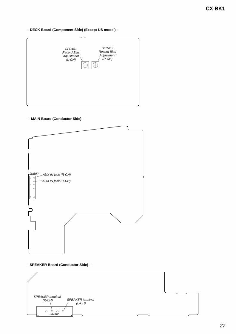
4. If these levels do not adjustment level, adjustment the SFR451(L-CH) and SFR452 (R-CH) to repeat steps 1 and 4.
Adjustment level: Playback output of 315 Hz to playback out-putof 10 kHz: 0 ± 1.0 dB (0 ± 4.5mV).
Adjustment Location: DECK board (Page 27)
+–
set
recordedportion
SPEAKER board SPEAKER terminal (JK502)
level meter
attenuator
set
MAIN boardAUX IN jack (JK602)
1) 315 Hz2) 10 kHz 50 mV (–23.8 dB)
600 Ω
blank tapeCN-123
AF OSC
Tape Speed CheckMode: Playback
1. Insert the WS-48B into the deck.2. Press the B button.3. Confirm that the frequency counter reads 3,000 ± 90 Hz.
Sample value of Wow and Flutter: 0.3% or less W.RMS (JIS)(WS-48B)
+–
set
test tapeWS-48B (3 kHz, 0 dB)
SPEAKER boardSPEAKER terminal (JK502)L-CH, R-CH
frequency counter
adjustment screw
27
CX-BK1
– DECK Board (Component Side) (Except US model) –
SFR451Record BiasAdjustment
(L-CH)
SFR452Record BiasAdjustment
(R-CH)
– MAIN Board (Conductor Side) –
AUX IN jack (R-CH)
AUX IN jack (R-CH)
JK602
– SPEAKER Board (Conductor Side) –
SPEAKER terminal (R-CH)
JK602
SPEAKER terminal (L-CH)
28
CX-BK1
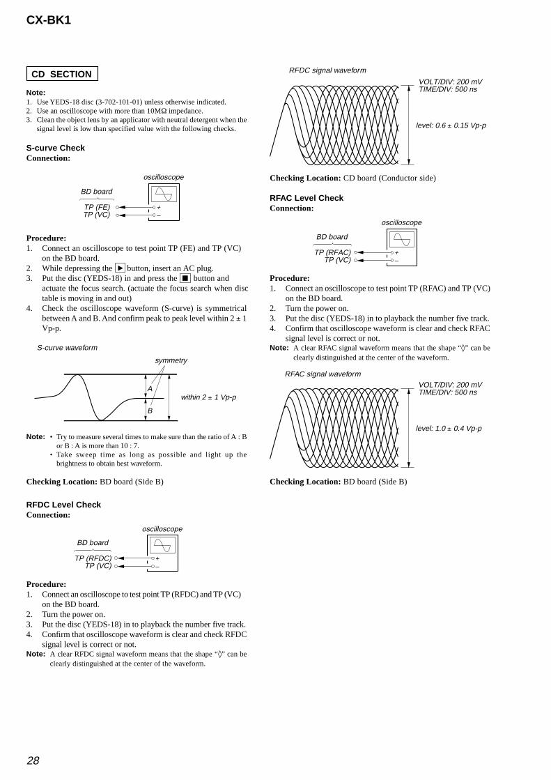
RFDC signal waveform
Checking Location: CD board (Conductor side)
CD SECTION
Note:1. Use YEDS-18 disc (3-702-101-01) unless otherwise indicated.2. Use an oscilloscope with more than 10MΩ impedance.3. Clean the object lens by an applicator with neutral detergent when the
signal level is low than specified value with the following checks.
RFDC Level CheckConnection:
Procedure:1. Connect an oscilloscope to test point TP (RFDC) and TP (VC)
on the BD board.2. Turn the power on.3. Put the disc (YEDS-18) in to playback the number five track.4. Confirm that oscilloscope waveform is clear and check RFDC
signal level is correct or not.Note: A clear RFDC signal waveform means that the shape “◊” can be
clearly distinguished at the center of the waveform.
+–
BD board
TP (RFDC)TP (VC)
oscilloscope
VOLT/DIV: 200 mVTIME/DIV: 500 ns
level: 0.6 ± 0.15 Vp-p
RFAC Level CheckConnection:
Procedure:1. Connect an oscilloscope to test point TP (RFAC) and TP (VC)
on the BD board.2. Turn the power on.3. Put the disc (YEDS-18) in to playback the number five track.4. Confirm that oscilloscope waveform is clear and check RFAC
signal level is correct or not.Note: A clear RFAC signal waveform means that the shape “◊” can be
clearly distinguished at the center of the waveform.
RFAC signal waveform
Checking Location: BD board (Side B)
+–
BD board
TP (RFAC)TP (VC)
oscilloscope
VOLT/DIV: 200 mVTIME/DIV: 500 ns
level: 1.0 ± 0.4 Vp-p
S-curve CheckConnection:
Procedure:1. Connect an oscilloscope to test point TP (FE) and TP (VC)
on the BD board.2. While depressing the button, insert an AC plug.3. Put the disc (YEDS-18) in and press the button and
actuate the focus search. (actuate the focus search when disctable is moving in and out)
4. Check the oscilloscope waveform (S-curve) is symmetricalbetween A and B. And confirm peak to peak level within 2 ± 1Vp-p.
S-curve waveform
Note: • Try to measure several times to make sure than the ratio of A : Bor B : A is more than 10 : 7.
• Take sweep time as long as possible and light up thebrightness to obtain best waveform.
Checking Location: BD board (Side B)
+–
BD board
TP (FE)TP (VC)
oscilloscope
A
B
symmetry
within 2 ± 1 Vp-p
B
x
29
CX-BK1
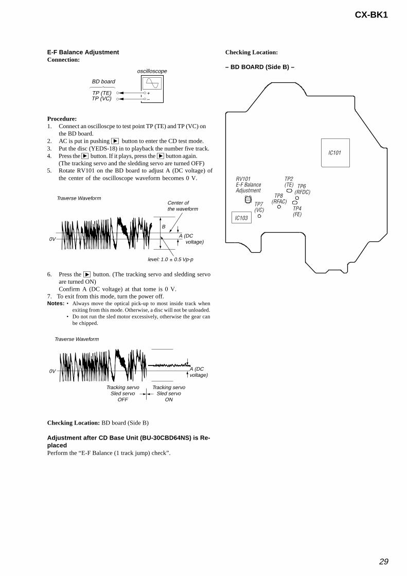
Checking Location: BD board (Side B)
Adjustment after CD Base Unit (BU-30CBD64NS) is Re-placedPerform the “E-F Balance (1 track jump) check”.
+–
BD board
TP (TE)TP (VC)
oscilloscope
Traverse Waveform
0V
B
level: 1.0 ± 0.5 Vp-p
Center of the waveform
A (DC voltage)
Traverse Waveform
0V
Tracking servoSled servo
ON
A (DC voltage)
Tracking servoSled servo
OFF
6. Press the button. (The tracking servo and sledding servo are turned ON)Confirm A (DC voltage) at that tome is 0 V.
7. To exit from this mode, turn the power off.Notes: • Always move the optical pick-up to most inside track when
exiting from this mode. Otherwise, a disc will not be unloaded.• Do not run the sled motor excessively, otherwise the gear can
be chipped.
E-F Balance AdjustmentConnection:
Procedure:1. Connect an oscilloscpe to test point TP (TE) and TP (VC) on
the BD board.2. AC is put in pushing B button to enter the CD test mode.3. Put the disc (YEDS-18) in to playback the number five track.4. Press the button. If it plays, press the button again.B
(The tracking servo and the sledding servo are turned OFF)5. Rotate RV101 on the BD board to adjust A (DC voltage) of
the center of the oscilloscope waveform becomes 0 V.
Checking Location:
– BD BOARD (Side B) –
B
B
IC101
TP7(VC)
IC103
RV101E-F BalanceAdjustment
TP8(RFAC)
TP6(RFDC)
TP4(FE)
TP2(TE)

30
CX-BK1
MEMO
CX-BK1
3131
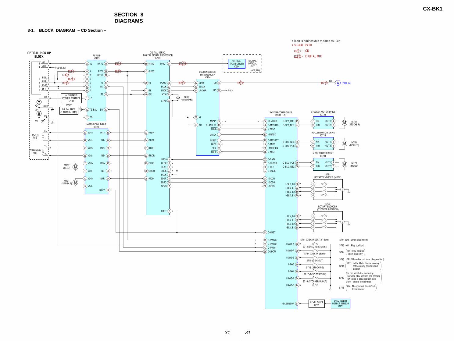
SECTION 8DIAGRAMS
8-1. BLOCK DIAGRAM – CD Section –
OPTICALTRANSCEIVER
IC604
OPTICAL PICK-UPBLOCK
PD1
PD2
I5-10
I1-6
LD
VC
VCC
7
5
3
1
2
4 VDD (3.3V)
GND
PD
VR
FOCUSCOIL
TRACKINGCOIL
RF AMPIC103
VC27
A6B7C8D9E10F11
LD1
PD2
MOTOR/COIL DRIVEIC102
VO1+52
VO1-47
VO2+56
VO2-55
VO3+2
VO3-1
M102(SLED)
M101(SPINDLE)
VO4+10
VO4-5
F+
F-
T+
T-
35IN1+
34IN1-
32IN2+
31IN2-
27IN3+
26IN3-
24IN4R
8STBY
MDP25
SRDR30
SFDR29
TRDR32
TFDR31
FRDR34
FFDR33
DIGITAL SERVO,DIGITAL SIGNAL PROCESSOR
IC101
64D OUTRFAC50
29RFDCI28RFDC
16FE
17FEI
12SWTE_BAL
RFDC43
FE39
TE41SE40
66PCMD
26RO
4DATA
R-CH
6CLOK
5XLAT
77SQCK
8SCLK
15SCOR
76SQSO
2XRST
O-DATA52O-CLOCK55O-XLT60O-SQCK57
I-SCOR21I-SQSO56
7SENS I-SENS58
SYSTEM CONTROLLERIC901 (1/3)
85O-LOD_NEG
O-LOD_POS
O-SLD_POS
O-SLD_NEG
74
I-D_SENSOR
I-SW5-B
I-SW5-A
I-SW4
I-SW3
I-SW2-A
I-SW2-B
I-SW1-A
15RF AC
18TE
D/A CONVERTER,MP3 DECODER
IC104
SDIO12 23LO
67BCLK BCKIA13
65LRCK LRCKIA14
71XTAI
72XTAO
XI62
XO635MIDIO
STAND BY
6MICK
7MIACK
39REQ
1RESET
19
75O-ELV_POS
O-ELV_NEG
IO-MIDIO
O-MP3STB
64
O-MICK
O-MICS
O-MILP
62
38
I-MIACK37
O-MP3RST19
3 5I-MP3REQ65
O-XRST61
4 66
MICS
MILP
O-PWM349O-PWM251O-PWM147O-LDON59
73
88
89
70
19
RV101
X20116.9344MHz
OUT1FIN
OUT2RIN
STOCKER MOTOR DRIVEIC721
M761(STOCKER)M7
9
4
287
77
OUT1FIN
OUT2RIN
ROLLER MOTOR DRIVEIC711
M781(ROLLER)M7
9
4
2
7686
OUT1FIN
OUT2RIN
MODE MOTOR DRIVEIC701
S771ROTARY ENCODER (MODE)
M771(MODE)M7
9
4
2
S713 (DISC IN (8/12cm))
S714 (DISC IN (8cm))
S715 (DISC OUT)
S716 (STOCKER IN/OUT)
S711 (DISC INSERT(8/12cm))
S717 (DISC POSITION)
S718 (STOCKING)
1
G2
3
4
69
90
67
68I-ELV_E3I-ELV_E2
I-ELV_E1I-ELV_E0
I-SLD_E3I-SLD_E2
I-SLD_E1I-SLD_E0
S702ROTARY ENCODER
(STOCKER POSITION)
1
2
3
4
82
79
83
80
78
84
81
(ON : When disc insert)S711
S713
S714
S715
S717
S718
(ON : When disc out from play position)
In the midst disc is moving between play position and stockerON : disc is play position sideOFF : disc is stocker side
OFF: In the Midst disc is movingbetween play position and stocker
(ON : Play position)
(8cm disc only)ON : Play position
S716 from stockerON : The moment disc in/out
G
AUTOMATICPOWER CONTROL
Q101
E-F BALANCE(1 TRACK JUMP)
M
M
CD-LA (Page 32)
• SIGNAL PATH
: CD
: DIGITAL OUT
• R-ch is omitted due to same as L-ch.
LEVEL SHIFTQ731
DISC INSERTDETECT SENSOR
IC751
DIGITALOPTICAL
OUT
(AEP, UK)
CX-BK1
3232
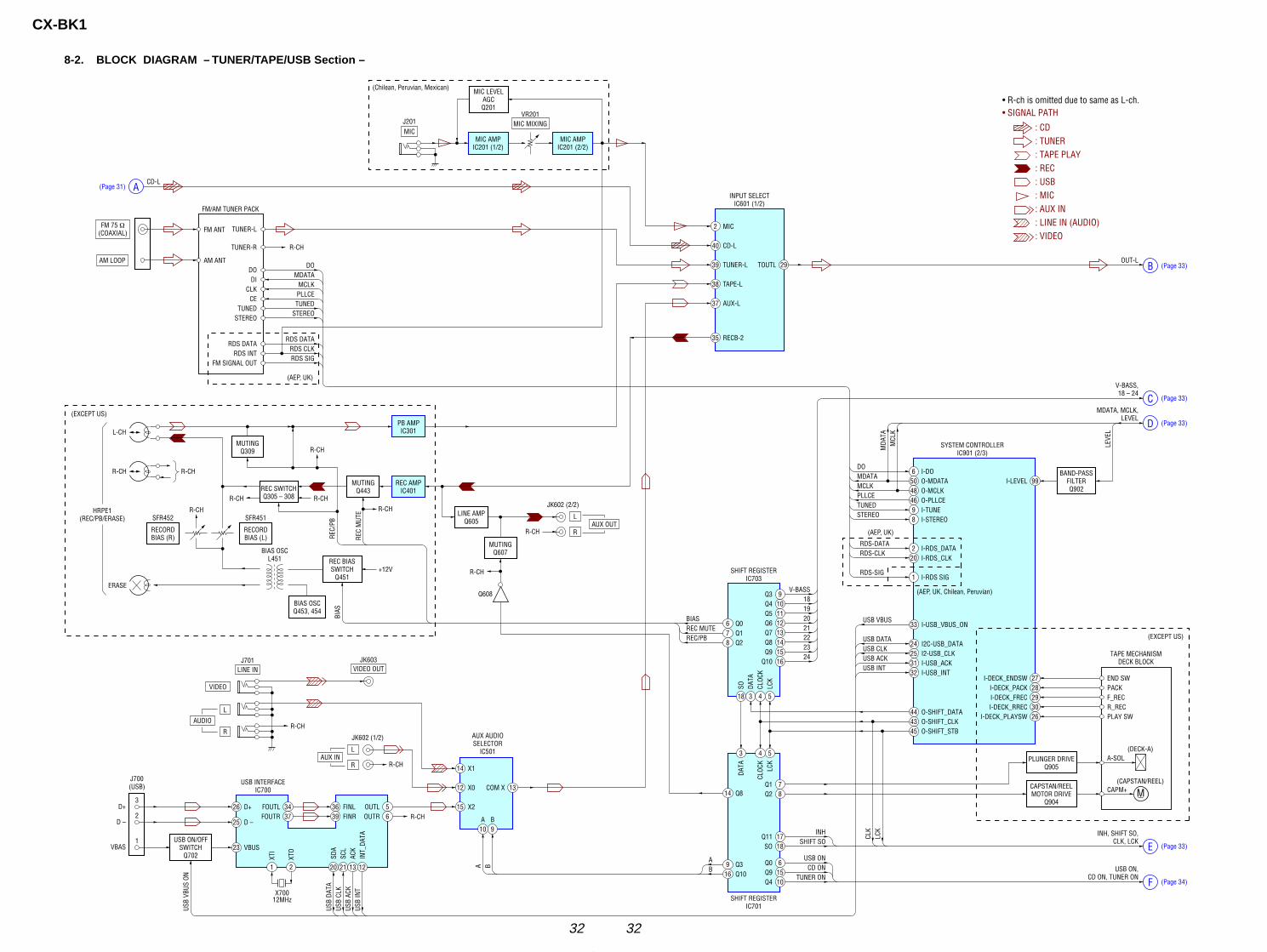
8-2. BLOCK DIAGRAM – TUNER/TAPE/USB Section –
• SIGNAL PATH
: CD: TUNER: TAPE PLAY: REC: USB: MIC: AUX IN: LINE IN (AUDIO): VIDEO
50 O-MDATA48 O-MCLK46 O-PLLCE9 I-TUNE8 I-STEREO
1 I-RDS SIG
2 I-RDS_DATA20 I-RDS_CLK
6 I-DO
34FOUTL37
20
FOUTR
SDA
21
SCL
13
ACK
12
INT_
DATA
USB
INT
5OUTL
13
10 9
COM X
BA6OUTR26 D+ 36 FINL 15 X2
12 X0
14 X1
39 FINR25 D –
23 VBUS
• R-ch is omitted due to same as L-ch.
FM/AM TUNER PACK
AM LOOP
FM ANT
AM ANT
TUNER-L
TUNER-R
CEPLLCE
R-CH
TUNEDTUNED
STEREOSTEREO
DODO
DIMDATA
CLKMCLK
PLLCETUNEDSTEREO
DOMDATAMCLK
RDS DATARDS DATA
RDS INTRDS CLK
FM SIGNAL OUTRDS SIG
MDA
TAM
CLK
RDS-DATARDS-CLK
RDS-SIG
33 I-USB_VBUS_ONUSB VBUS
24 I2C-USB_DATAUSB DATA
25 I2-USB_CLKUSB CLK
31 I-USB_ACKUSB ACK
32 I-USB_INT
44 O-SHIFT_DATA
USB INT
USB ONCD ON
TUNER ON
INHSHIFT SO
CLK
LCK
BIAS OSCL451 REC BIAS
SWITCHQ451
BAND-PASSFILTERQ902
CAPSTAN/REELMOTOR DRIVE
Q904
USB ON/OFFSWITCH
Q702
+12V
USB INTERFACEIC700
AUX AUDIOSELECTOR
IC501
16
18 3
Q1015Q914Q813Q712Q611Q510Q49Q3
LCK
CLOC
KDA
TASO
4 5
8 Q27 Q16 Q0
SHIFT REGISTERIC703
18
3
SO17Q11
10Q415Q96Q0
8Q2
27I-DECK_ENDSW
99I-LEVEL
28I-DECK_PACK29I-DECK_FREC30I-DECK_RREC26I-DECK_PLAYSW
7Q1
LCK
CLOC
K
DATA
4 5
16 Q109 Q3
14 Q8
SHIFT REGISTERIC701
BIAS OSCQ453, 454
MUTINGQ309
ERASE
J700(USB)
D+
D –
VBAS
HRPE1(REC/PB/ERASE)
R-CH
SFR451R-CH
R-CH
R-CH
R-CH
R-CH
R-CH
R-CH
JK602 (1/2)
L-CH
R-CH R-CH
REC SWITCHQ305 – 308
RECORDBIAS (L)
SFR452
RECORDBIAS (R)
R-CH
Q608
MUTINGQ443
PLUNGER DRIVEQ905
REC AMPIC401
PB AMPIC301
LINE AMPQ605
MUTINGQ607
43 O-SHIFT_CLK45 O-SHIFT_STB
LEVE
L
(AEP, UK)
(AEP, UK)
(AEP, UK, Chilean, Peruvian)
SYSTEM CONTROLLERIC901 (2/3)
FM 75 Ω(COAXIAL)
USB
ACK
USB
CLK
USB
DATA
USB
VBUS
ON
3
2
1
1 2
XTI
XTO
X70012MHz
REC/PBREC MUTEBIAS
V-BASS18192021222324
REC/
PB
REC
MUT
E
BIAS
BA BA
LINE INJ701 JK603
VIDEO
VIDEO OUT
AUDIO
L
R
AUX INL
R
R-CH
JK602 (2/2)
AUX OUTL
R
MIC AMPIC201 (1/2)
MIC AMPIC201 (2/2)
INPUT SELECTIC601 (1/2)
29TOUTL
VR201J201
40 CD-L
2 MIC
39 TUNER-L
38 TAPE-L
35 RECB-2
37 AUX-L
MIC LEVELAGCQ201
MICMIC MIXING
CD-LA
MDATA, MCLK,LEVEL
D (Page 33)
V-BASS,18 – 24
C (Page 33)
OUT-LB (Page 33)
(Page 31)
(Chilean, Peruvian, Mexican)
(EXCEPT US)
(EXCEPT US)
MM
TAPE MECHANISMDECK BLOCK
(CAPSTAN/REEL)
(DECK-A)
END SW
A-SOL
CAPM+
PACKF_RECR_RECPLAY SW
INH, SHIFT SO,CLK, LCK
E (Page 33)
USB ON,CD ON, TUNER ON
F (Page 34)

CX-BK1
3333
8-3. BLOCK DIAGRAM – AMP Section –
J521
POWER
THERMAL DETECT
POWER MONITOR
RY501
R-CH
PHONES
+–
–+
R
L
M301(FAN)
R-CH
R-CH
– VL
–VP
+VP
– VH
OVER LOADDETECT
Q505
THERMALDETECT
Q610, 611
OUTPUT LEVELDETECT
Q617, 622 – 624
ROTARYENCODER
S301
OVER CURRENTDETECT
Q013 RELAY DRIVEQ530
BIASQ507, 509FEED BACK
SWITCHQ625
FINAL DRIVEQ531, 533
SWITCHINGQ619
SWITCHINGQ618
FAN MOTORDRIVE
Q301 – 303
+
+
R-CH
R-CH
+
HOLDQ012
+
+
TH501, 502R-CH
R-CHR-CH
CASCADEQ511, 513, 515
PRE DRIVEQ517
MUTINGQ525
+MUTINGCONTROL
Q527
CURRENTMIRROR
Q521, 523
FREQUENCYCONTROL
Q614 – 616
BBE ON/OFFCONTROL
Q623
R-CH
D611
+VL
+VHOUTPUT LEVEL
DETECTQ620, 621
1
7
6
BASS BOOST ENHANCERIC603
ELECTRICAL VOLUMEIC601 (2/2)
INA
BBE
14
VREF
12
GOUT
OUTA 25OUT 2
27BB_A226BB_B2
28 VOLIN2
13
GIN
BOOSTCONTROL
Q617 – 620
BOOSTCONTROL
Q624
+R-CH
OUT-L
V-BASS,18 –24
21
DATA
22
CLOC
KLE
VEL
MCL
KM
DATA
19
SAOU
T
39
O-M
UTE
98
I-POW
ER_M
ONI
42I-HEADPHONE
40O-POWER
232221 24201918
LCKCLKSHIFT SO
LED631 – 635(DISC INDICATOR 1 – 5)
V-BA
SS
G (Page 34)
H (Page 34)
J (Page 34)
B(Page 32)
C(Page 32)MDATA, MCLK,LEVEL
D(Page 32)
INH, SHIFT SO,CLK, LCK
E(Page 32)
MM
• SIGNAL PATH: TUNER
• R-ch is omitted due to same as L-ch.
76
7978
80
LIQUID CRYSTALDISPLAYLCD001
67 –
70
1 –
65
COM
1 –
COM
4S1
– S
65
OSC
C105, R101
LCD DRIVERIC001
OSC
16
6 –
15
Q0 –
Q9
Q10
DICLCE
77
3
INH
DATA4 CLK5 LCK
53 O-LCD_DATA54 O-LCD_CLK63 O-LCD_CE
18 SO 93 I-RE_VOL
2 DATA3 CLK4 LCK
INH
S311 – 320, 331 – 339,S341 – 344
17 18
X90132.768kHz
XT1
XT2
14 15
X9025MHz
X1 X2
23 I-RMCREMOTE CONTROL
RECEIVERIC603
LCKCLK
LED203
LED DRIVEIC602
i-Bass
34
STBY
LED202STANDBY/ON
VOLUME
ROTARYENCODER
S30292 I-RE_BASBASS
ROTARYENCODER
S30391 I-RE_TRETREBLE/MIDDLE
ROTARYENCODER
S30494 I-RE_JOGMULTI JOG
LED204 – 221(ILLUMINATION)
12
6 –
11
Q1 –
Q6
Q797
– 9
5
I-KEY1 – I-KEY3
LED251 – 254(LCD BACKLIGHT)13
, 14
Q8, Q
9
LED601(DISC SLOT ILLUMINATION)
LED DRIVEIC601
41I-POWER_DOWN
16RESET
POWER_DOWN
RESET
SYSTEM CONTROLLERIC901 (3/3)
LED DRIVEQ601 – 605
5 SPEAKERJK502
CX-BK1
3434
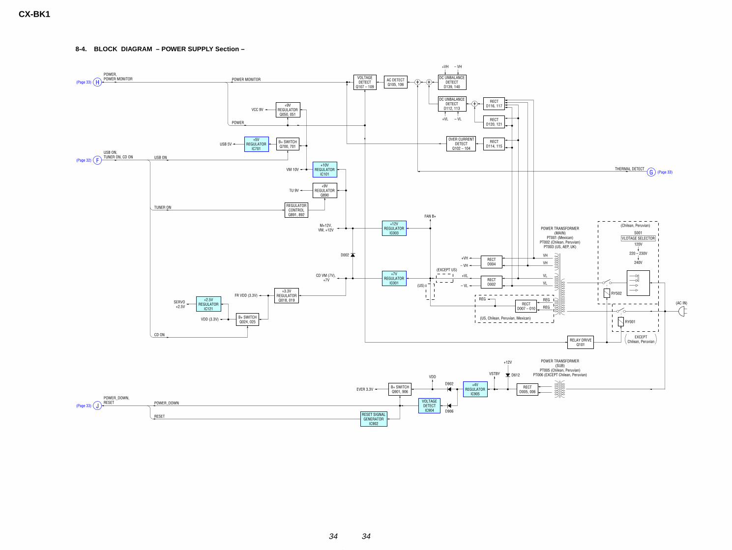
8-4. BLOCK DIAGRAM – POWER SUPPLY Section –
+7VREGULATOR
IC001
POWER TRANSFORMER(SUB)
PT005 (Chilean, Peruvian)PT006 (EXCEPT Chilean, Peruvian)
POWER TRANSFORMER(MAIN)
PT001 (Mexican)PT002 (Chilean, Peruvian)
PT003 (US, AEP, UK)
RECTD002
RY502
RY001
VL
VL
RECTD004
RECTD120, 121
RECTD114, 115
RECTD116, 117
VSTBY D612
+12V
VH
VH
RECTD007 – 010
REG
– VL
REG
+VL
– VH
+VH
+3.3VREGULATORQ018, 019
+9VREGULATOR
Q890
DC UNBALANCEDETECT
D112, 113
+12VREGULATOR
IC003
REGULATORCONTROLQ891, 892
REG
B+ SWITCHQ901, 906
RELAY DRIVEQ101
RECTD005, 006
+4VREGULATOR
IC905
VDD
D906
EVER 3.3VD902
RESET SIGNALGENERATOR
IC902
VOLTAGEDETECTIC904
B+ SWITCHQ024, 025
B+ SWITCHQ700, 701
AC DETECTQ105, 106
D002
FR VDD (3.3V)+2.5V
REGULATORIC121
SERVO+2.5V
TU 9V
+10VREGULATOR
IC101
+9VREGULATORQ050, 051
VOLTAGEDETECT
Q107 – 109
OVER CURRENTDETECT
Q102 – 104
+5VREGULATOR
IC701
VM 10V
USB 5V
VCC 9V
POWER
POWER MONITOR
CD VM (7V), +7V
M+12V,VM, +12V
VDD (3.3V)
POWER_DOWN
CD ON
TUNER ON
USB ON
RESET
(AC IN)
120V
220 – 230V
240V
(Chilean, Peruvian)
EXCEPTChilean, Peruvian
VLOTAGE SELECTORS001
FAN B+
+VL – VL
DC UNBALANCEDETECT
D139, 140
+VH – VH
+
++
THERMAL DETECTG (Page 33)
POWER,POWER MONITOR
H(Page 33)
USB ON,TUNER ON, CD ON
F(Page 32)
POWER_DOWN,RESET
J(Page 33)
(US, Chilean, Peruvian, Mexican)
(US)
(EXCEPT US)

CX-BK1
3535
8-5. NOTE FOR PRINTED WIRING BOARDS AND SCHEMATIC DIAGRAMS
Note on Schematic Diagram:• All capacitors are in µF unless otherwise noted. pF: µµF
50 WV or less are not indicated except for electrolyticsand tantalums.
• All resistors are in Ω and 1/4 W or less unless otherwise
specified.• f : internal component.• 2 : nonflammable resistor.• C : panel designation.
• A : B+ Line.• B : B– Line.• H : adjustment for repair.• Voltages and waveforms are dc with respect to ground
under no-signal (detuned) conditions.– BD Board –no mark : CD PLAY– DECK Board –no mark : TAPE PLAY( ) : TAPE REC– USB AUX Board –no mark : USB– Other Board –no mark : TUNER( ) : CD PLAY⟨⟨ ⟩⟩ : TAPE PLAY : TAPE REC[ ] : USB
∗ : Impossible to measure• Voltages are taken with a VOM (Input impedance 10 MΩ).
Voltage variations may be noted due to normal produc-tion tolerances.
• Waveforms are taken with a oscilloscope.Voltage variations may be noted due to normal produc-tion tolerances.
• Circled numbers refer to waveforms.• Signal path.
F : TUNERJ : CDc : DIGITAL OUTE : TAPE PLAYd : USBj : RECN : MICG : AUX INq : LINE IN (AUDIO)r : VIDEOAbbreviationE51 : Chiliean and Peruvian modelsMX : Mexican model
Note: The components identified by mark 0 or dotted linewith mark 0 are critical for safety.Replace only with part number specified.
• Circuit Boards Location
Note on Printed Wiring Boards:• X : parts extracted from the component side.• Y : parts extracted from the conductor side.• a : Through hole.• f : internal component.• : Pattern from the side which enables seeing.(The other layers' patterns are not indicated.)
Caution:Pattern face side: Parts on the pattern face side seen from(Side B) the pattern face are indicated.Parts face side: Parts on the parts face side seen from(Side A) the parts face are indicated.
tuner unitmain board
speaker board
ACDC board
PT board
AMP board
deck board (EXCEPT US)
SW (3) board
speaker motor board
SW (4) board
roller motor board
connector board
BD board
mode motor board
headphone board
right button (2) boardMIC board
LED board
jog board
USB AUX board
key LED RMC board
LCD VOL board
left button board
right button (1) board
SW (1) boardSW (2) board
CX-BK1
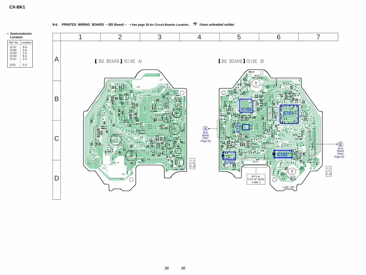
3636
8-6. PRINTED WIRING BOARD – BD Board – • See page 35 for Circuit Boards Location. :Uses unleaded solder.
IC101 B-6IC102 C-6IC103 C-5IC104 B-5IC121 C-5
Q101 C-3
• SemiconductorLocation
Ref. No. Location
E
TP7(VC)
TP4(FE)
TP2(TE)
TP8(RFAC)
TP6(RFDC)
A
A-MAX. 3
B
CN507
R284 C272
1 2
A
B
C
D
3 4 5 6 7
IC104IC101
IC12
1
IC102
IC103
(Page 43)
(Page 43)
CX-BK1
3737
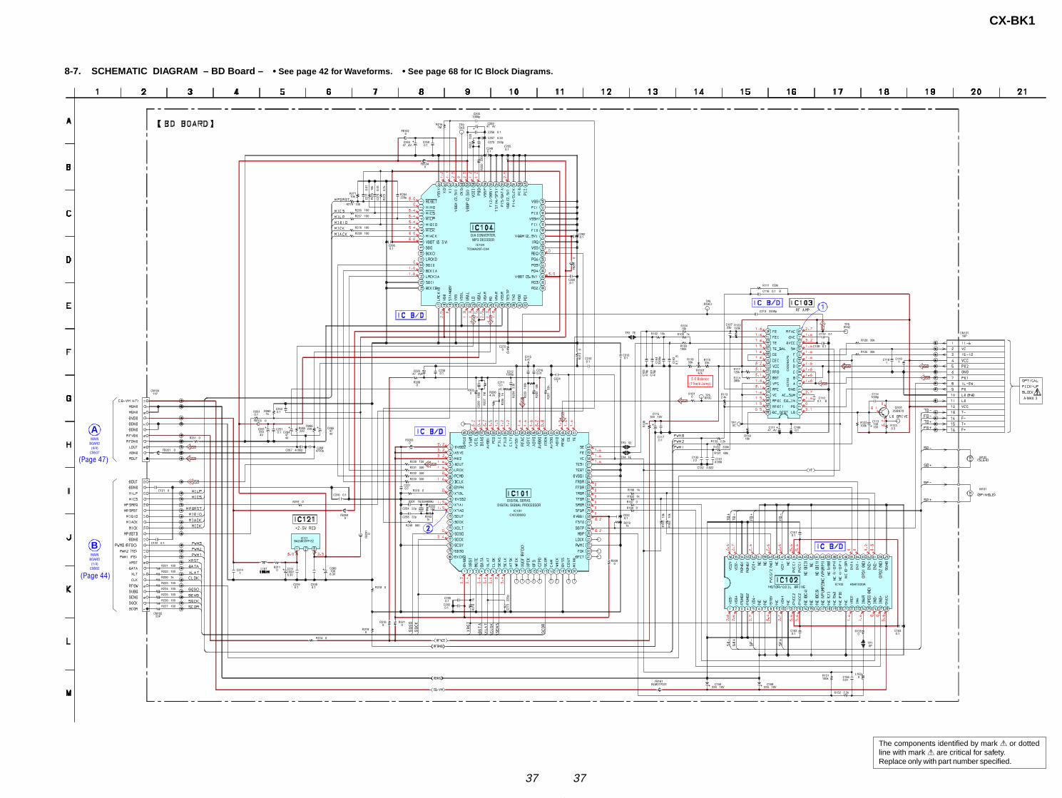
8-7. SCHEMATIC DIAGRAM – BD Board – • See page 42 for Waveforms. • See page 68 for IC Block Diagrams.
RV101
IC102
CN102
R116
CN104
M101
M102
C152
CN101
R131
R118
R111
C103
C101
C111 C108
C109
C102
C117
R123
C116
R114
C132
R122
R133
C115
C107
Q101
C110
R132
R103
R120R104
C153
R220
C151
R221
R226
R225
R227
R222
R224
R223
TP3
TP4
TP2
R20
2
R20
1
R252
R266
R21
8
R20
3
C226
IC101
C202
C205
C230
R151
C209
R20
4
R219
C112
R206
TP7
R265
TP5
R253C258
TP9
TP8
TP6
C104
C212
C114
C229
C213
C292
R25
0
C255R25
1
R216
C259
R284
C253
R279
R255
R257
R276
R259
FB161
C251
C227
C222
C208
C203
R168
R166
C150 C169
C231
C268
R249
R230
R260
C122
C316
R233
R231
R232
C156
C269
C263
R126
R125
R117
R113
L163
R309
R167
R169
R101
C113
IC103
R308 C211
FB203
R310
FB20
1
FB204
IC121
C260
R31
3
R318
R321
R319
R316
R314
L101 R311C314
C261 C265
FB351
IC104
C121
FB29
1
R291
R271
R27
2
C274
R27
5
C271
C267
FB103
R261
FB102
C249
FB104
C270C257
C256
C250
X201
C254
R20
5
C216
C224
C273
C313
C133 C131
C118 C119
R155
R20
7
C215
C264
R351
C310
R16
3
R16
2
R19
9TP1
R152
R105R102
47k
33k
0.1
16P
68k
10k
150k
470p
470p
47 4V 0.1
0.1
0.1
B
0.1
3.3
0.1 B
390k
0.022
100k
2.2k
100 10V
33p
2SB970
0.1 B
330k
100k
120k15k
0.1
1k
0.1
100
100
100
100
100
100
100
SE
FE
TE
10k
33k
1k
100k
47 4V
CXD3068Q
0.1
0.1
0.1
1k
0.1
VC
RFACI
CKO
RFAC
RFDC
3300
p
1000p
BLM21P331
0.1
220 10V
150
0
0
0
10010V
CX
A2647N
0
0
0
0.01
1
220p
2.2 0.068
1 10.47
B 0.1
0SP
1k15k
AN41020A
100k
220220
1k
1M
22p
100p 4.7k
3.3k
23P
11P
1k
1k
1M
220
220
100
100
1k
100
100
1000p
0.10.1
0.1
0.1
220p
1500p
0.1 0.1
3300p
100
0.1
0.1
47 4V
47 4V
220 10V
10006.3V
4700p
560
0.1
0.1
330
330
330
0.01
39k
39k
120k
2.4k
0
0
0 0.1
0
0
0
0
BA25BCOFP-E2
1006.3V
0
0
0
0
01
2204V
474V
0
TC94A20F-CX4
0
0
10k
4.7k
0.01
10k
0.01
4700p
0
0.1
0
0.1
0
220p0.33
0.1
0.1
16.9344MHz
22p
1k
0.1
0
1M
474V0
10k
10k
2.2k
R11533k
C2660.1
R3030
C2720
E-F Balance(1Track Jump)
AMAIN
BOARD(4/4)
CN507
BMAIN
BOARD(1/4)
CN902
D/A CONVERTER,MP3 DECODER
DIGITAL SERVO,DIGITAL SIGNAL PROCESSOR
A-MAX. 3
(Page 47)
(Page 44)
The components identified by mark 0 or dottedline with mark 0 are critical for safety.Replace only with part number specified.
CX-BK1
3838
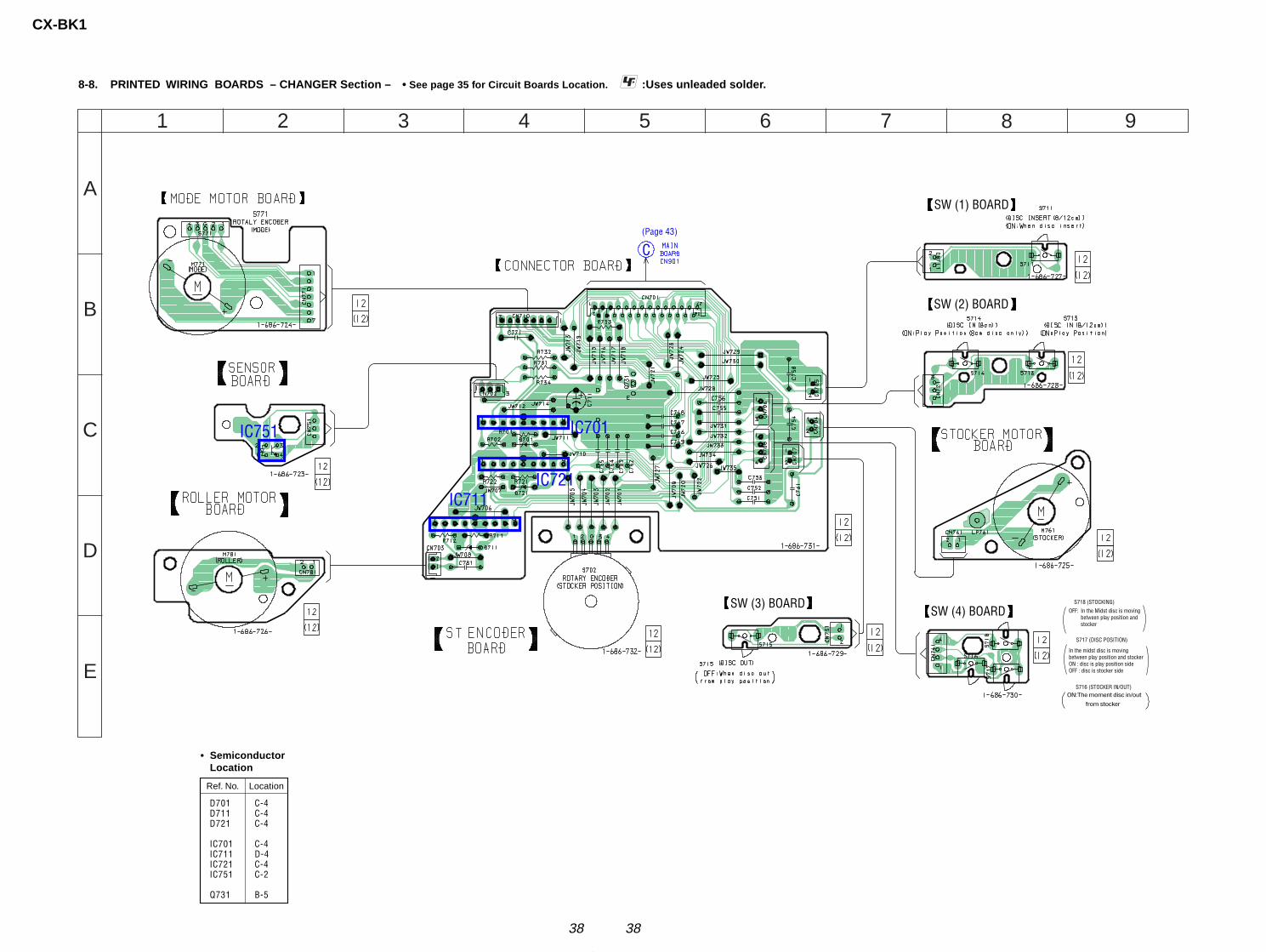
8-8. PRINTED WIRING BOARDS – CHANGER Section – • See page 35 for Circuit Boards Location. :Uses unleaded solder.
D701 C-4D711 C-4D721 C-4
IC701 C-4IC711 D-4IC721 C-4IC751 C-2
Q731 B-5
• SemiconductorLocation
Ref. No. Location
In the midst disc is moving between play position and stockerON : disc is play position sideOFF : disc is stocker side
OFF: In the Midst disc is movingbetween play position and stocker
S716 (STOCKER IN/OUT)
S717 (DISC POSITION)
S718 (STOCKING)
ON:The moment disc in/out
from stocker
C
SW (3) BOARDSW (4) BOARD
SW (2) BOARD
SW (1) BOARD
1 2
A
B
C
D
E
3 4 5 6 7 98
IC701
IC721IC711
IC751
(Page 43)
CX-BK1
3939
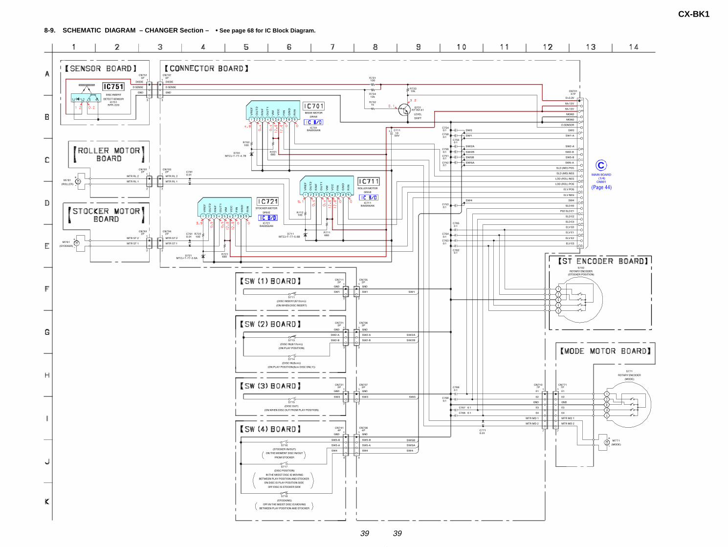
8-9. SCHEMATIC DIAGRAM – CHANGER Section – • See page 68 for IC Block Diagram.
R733
R711 C764
C763
C762
C765
C769
C753
C752
C751
C755
C756
C758
C754
S713
S714
S718
S717
S716
S715
S711
CN710
M771
Q731
R731
R734
R732
R702
R701D701
C711
R712
D721 R721
D711C761 R722
C781
CN704
CN703
CN702
C768
C766
C767
CN701
C771
CN771
S702
S771
IC701
IC711
IC721
CN751
IC751
CN781
CN761
M781
M761
CN741 CN708
CN731 CN707
CN721 CN706
CN711 CN705
10k
680 0.1
0.1
0.1
0.1
0.1
0.1
0.1
0.1
0.1
0.1
0.1
0.1
7P
RT1N141
100
12k
1k
100
680MTZJ-T-77-4.7B
1050V
100
MTZJ-T-77-3.6A 680
MTZJ-T-77-5.6B0.01 100
0.01
2P
2P
3P
0.1
0.1
0.1
27P
0.01
7P
BA6956AN
BA6956AN
BA6956AN
3P
RPR-220
2P
2P
4P 4P
2P 2P
3P 3P
2P 2P
SW1
SW1
SW2B
SW2B
SW2A
SW2A
SW3
SW3
SW5B
SW5A
SW5A
SW4
SW5B
SW4
GND
E1
E2
E3
E4
GND
GND
D SENSE D SENSE
DIODE DIODE
E1
E2
E3
E4
GND
MTR MD 2
MTR MD 1
SW2-A
SW1
SW2-B
SW3
SW5-A
SW4
SW5-B
GND
GND
GND
GND
SW3
D+3.3V
M+12V
MGND
MGND
D.SENSOR
SW1-A
SW2-A
SW2-B
SW5-B
SW5-A
SW4
SLD (MD) POS
SLD (MD) NEG
LOD (ROL) NEG
LOD (ROL) POS
SLD E0
P02 SLD E1
SLD E2
SLD E3
ELV E1
ELV E0
ELV NEG
ELV POS
M+12V
ELV E2
ELV E3
MTR MD 2
MTR MD 1
MTR ST 2
MTR ST 1
MTR RL 2
MTR RL 1
MTR ST 2
MTR ST 1
MTR RL 1
MTR RL 2
SW2-A
SW1
SW2-B
GND
GND
SW3
GND
SW5-A
SW4
SW5-B
GND
OU
T2
GN
D
OU
T1
VC
C
VR
EF
RN
F
VM
FIN
RIN
OU
T2
GN
D
OU
T1
VC
C
VR
EF
RN
F
VM
FIN
RIN
OU
T2
GN
D
OU
T1
VC
C
VR
EF
RN
F
VM
FIN
RIN
(MODE)
(STOCKER POSITION)ROTARY ENCODER
ROTARY ENCODER
(MODE)
LEVEL
SHIFT
MODE MOTOR
DRIVE
DRIVE
ROLLER MOTOR
DRIVE
STOCKER MOTOR
DISC INSERT
DETECT SENSOR
(ROLLER)
(STOCKER)
(DISC INSERT(8/12cm))
(ON:WHEN DISC INSERT)
(ON:PLAY POSITION)
(DISC IN(8/12cm))
(DISC IN(8cm))
(ON:PLAY POSITION(8cm DISC ONLY))
(DISC OUT)
(ON:WHEN DISC OUT FROM PLAY POSITION)
(STOCKER IN/OUT)
ON:THE MOMENT DISC IN/OUT
FROM STOCKER
(DISC POSITION)
IN THE MIDST DISC IS MOVING
BETWEEN PLAY POSITION AND STOCKER
ON:DISC IS PLAY POSITION SIDE
OFF:DISC IS STOCKER SIDE
(STOCKING)
OFF:IN THE MIDST DISC IS MOVING
BETWEEN PLAY POSITION AND STOCKER
+
-
+
-
1
3
1
3
1
2
1
2
1
2
1
2
1
2
1
1 1
3 3
2
1
2
1
1 1
4 4
2
1 1
7 7
+
-
MAIN BOARD (1/4)
CN901
C
3 . 2
IC751
(Page 44)

CX-BK1
4040
8-10. PRINTED WIRING BOARD – DECK Board (Except US model) – • See page 35 for Circuit Boards Location. :Uses unleaded solder.
D401 F-3
IC301 E-7IC401 E-3
Q305 E-4Q306 D-5Q307 E-4Q308 F-4Q309 E-5Q310 E-5Q443 E-3Q444 F-3Q451 B-6Q453 B-5Q454 B-5
• SemiconductorLocation
Ref. No. Location
JW30
1
JW30
2
JW303
JW304
JW305
JW306
JW308
JW30
9
JW31
0
JW312
JW314
JW31
5
JW31
6
JW317
Q305
SFR452
L451
Q308
Q307
C307
SFR451
C457
C411
C412
C401
C402
C308
C452
Q453
Q454
Q451
R460
C317C318
EP301
CN008
R457
C360
JW307
C315
CN30
2
JR318
JR319
JR320
C303
C304
R303
R304
JR303
JR304
Q309
Q310
R305
R307
R308
C326
C309
C310
JR401
R319
R399
C399
R423
R424
R401
Q306
R421
R422
C409
C410
R419
R420
Q443
Q444
R417
R418
D401
C413
R413
R414
R415
R416
R407
R410
R409
R408
R411
R412
C405
C406
C407
C408
C327
R402
R403
R404
R405
R406
R465
C403
R466
C404
IC301
C314
R310
R309
R315 R316
R317R318
R313
R314
C462
C461
C458
C459
C456
C454
C455
C453 R453R455
R456
R458
R459
R454
C460
R375
R376
FB301
R321
R322
C325R306
C313
JR402
JR302JR321
JR322
R425
R323
IC401
1
4
8
5
5
8
4
1
DECK BOARD
1-688-685-
12
(12)
DMAIN
BOARDCN009
1
8
R-CH L-CH ERASE
E
E
E
E
E
G
G
D
S
D S
G D S
E
BIAS OSC
E
E
(CHASSIS)
1 2 3 4 5 6 7 8 9
B
A
C
D
E
F
G
18
(Page 43)

CX-BK1
4141
8-11. SCHEMATIC DIAGRAM – DECK Board (Except US model) – • See page 42 for Waveforms.
CN008
HRPE301
CN302
EP301
JR304
JR303
R404
FB301
R406C404
R402
IC401(2/2)
R412
R415
R403
C403 R405 R407 R409
C411C405
C406 C412
R410R408
R401
C401
R323
IC301(1/2)
R314 C314
R316
IC301(2/2)
C315R375
R315
R305
R308C310
R310
C308
R307C309
C307
R309
R306
C304
R304
C303
R303
C318R322
C360
R376
C317R321
R318
R317
C399
C410R422R417
C409
R419
Q443R421
R423
Q307
Q305
R399
C413
C327
Q308
Q306
R424R420
R418
Q444
R319
C462C461
Q309
Q310
JR401
C456
C452
C325
C459
C458
C457
SFR452
SFR451
L451
Q453
Q454
R458
C460
R453
R460
R459
Q451
R457
C326
C407
C408 R425
R416
IC401(1/2)R413
R411
R414
D401
R313 C313
R454
C454
C455
C453
R456
R455
C402
11P
8P
0
0
1k
0
47k82p
120k
NJM14558MTE2
15k
680
1k
82p 47k 1k 1.2k
1050V0.01
0.01 1050V
1.2k1k
120k
0.150V
100
NJM14558MTE2
18k 0.0068
390k
NJM14558MTE2
22016V1.2k
390k
220k
47047p
56
10010V
47047p
10010V
56
3.9k
0.0012
82k
0.0012
82k
0.150V
0
22016V
1k
0.150V
0
1.2k
1.2k
470p
0.004722k10k
0.0047
1k
2SA1362G22k
18k
2SJ460
2SJ460
1M
0.1
0.1
2SJ460
KRC104S
18k1k
10k
2SA1362G
4.7k
390p390p
2SA1362G
2SA1362G
0
0.01
2225V 0.1
560p
0.001
0.0056
33K
33K
KTC3198GR
KTC3198GR
100k
0.1
3.3k
33
15
2SA1981Y
15
0.022
0.01
0.01 10k
680
NJM14558MTE2 2.2k
15k
2.2k
1SS355
18k 0.0068
8.2
0.0027
0.0027
0.0027
18k
18k
0.150V
A-GND
PB-L
REC-L
PB-R
REC-R
VM_A
REC/PB SW
REC-MUTE
DECK-D-GND
+12V
SS
S
5
6
7
4
8
1
3
2
O-BIAS
(CHASSIS)
(REC/PB/ERASE)
ERASE
R-CH
L-CH
MUTING
MUTING
Q305-308
REC SWITCH
MUTING
MUTING
BIAS OSC
BIAS OSC
Q453,454REC BIAS
SWITCH
REC AMP
PB AMP
8
1 2
3
7
4
5
6
R465 100K
R466100K
(Page 46)

CX-BK1
4242
qs Q453, 454 Collector (REC mode)
qd Q453, 454 Emitter (REC mode)
ws IC901 qk (XT2)
• Waveforms– BD Board –
1 IC103 qg (RFAC) (CD play mode)
2 IC101 us (XTAO)
1.2 Vp-p
3.9 Vp-p
59.1 ns
– DECK Board –
qa Q453, 454 Base (REC mode)
3.6 Vp-p
11.2 µs
10.9 Vp-p
11.4 µs
0.9 Vp-p
5.7 µS
– MAIN Board –
wa IC901 qg (X2)
2.4 Vp-p
200 ns
2.5 Vp-p
30.4 µs
– USB AUX Board –
ea IC700 2 (XTO) (USB mode)
37 Vp-p
84 ns
– LCD VOL Board –
ra IC001 uh (OSC)
1.5 Vp-p
21.5 µs
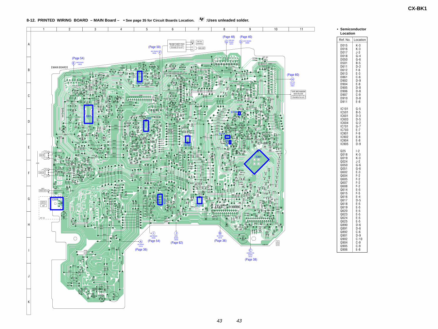
CX-BK1
4343
8-12. PRINTED WIRING BOARD – MAIN Board – • See page 35 for Circuit Boards Location. :Uses unleaded solder.
D015 K-3D016 K-3D017 J-3D018 G-4D050 G-6D501 B-5D611 D-2D612 F-6D613 E-3D861 C-6D902 D-9D904 E-8D905 D-8D906 D-8D907 C-9D910 D-8D911 E-8
IC101 G-5IC501 B-5IC601 D-3IC603 D-5IC604 G-2IC701 G-7IC703 E-7IC901 F-9IC902 E-8IC904 E-8IC905 D-9
Q25 I-2Q018 K-3Q019 K-3Q024 J-2Q050 G-6Q051 G-6Q602 E-3Q604 F-2Q605 F-2Q607 F-2Q608 F-2Q614 E-5Q615 F-5Q616 E-4Q617 D-5Q618 E-5Q619 E-5Q620 E-5Q623 E-5Q624 E-5Q625 E-5Q890 D-6Q891 D-6Q892 C-6Q901 D-9Q902 C-10Q904 C-9Q905 C-9Q906 E-8
• SemiconductorLocation
Ref. No. Location
JW633
JW903
JW904
JW909
JW910
JW915
JW91
7
JW92
1
JW92
2
JW92
4
JW92
5
JW930
JW931
JW932 JW934
JW935
JW936
JW937
JW94
1
JW94
2
JW94
3
JW944
JW946
JW947
JW948
JW949
JW956 JW958
JW959
JW960
JW966
JW968
JW97
6
JW98
0
JW98
1
JW04
8
JW04
9
JW05
0
JW996
JW52
3
JW95
4
JW95
5
JW95
3
JW950
JW975
JW982
JW99
2
JW99
3
JW99
4
JW967
JW970JW974
JW99
0
JW05
1
JW645
JW99
7
JW91
6
JW995
JW905
JW906
JW907
JW908
JW911
JW722
JW971
JW972
JW939
JW804
JW643
JW64
0
JW632
JW977
JW978
JW979
JW95
1
JW95
2
JW964
JW701
JW702
JW703
JW704
JW705
JW706
JW707
JW708
JW709
JW710
JW711
JW71
4
JW715
JW04
4
JW04
5
JW046
JW04
7
JW03
2
JW03
6
JW98
4
JW98
5
JW98
6
JW80
2
JW98
7
JW611
JW612
CN506
JW60
8
JW60
9
JW61
0
JW628
JW629
JW630
JW631JW613
JW616
JW614
JW602
JW01
8
JW02
1JW
022
JW024
JW02
9
JW03
0
JW03
1
JW717
JW00
4
JW60
7
JW604
JW60
5
JW60
6
JW603
JW61
5JW621
JW622
JW618
JW617JW620
JW61
9 JW637
JW63
8
JW62
7
JW64
7
JW64
8
JW64
9
JW65
0
JW52
2
JW525
JW526
JW65
1
JW51
2
JW51
3
JW51
4
JW52
7
JW53
1
JW53
2
JW53
4
JW536
JW54
0
JW54
1
JW54
2
JW545
JW546
JW547
JW55
3
JW02
3
JW05
2
JW053
JW054
JW055
JW056
JW06
2
JW06
3
JW070
JW071
JW072
JW073
JW074
JW805
JW55
4
JW555
JW03
5
JW03
8
JW80
3
JW914
JW963
JW652JW983
JW988
JW95
7
JW945
C933
C936
C934
C931
C927
C052
C050
Q051
IC10
1
CN00
6
C637
C627
JW01
1
CN905
CN507
C691
IC604
C629
C621
Q019
C634
C622
C640
C686C630
C687
R038
C693
R016
C632
C697
C625
C636
C628C626 C682
C631
C683
C692
C604
Q905
C603
C635
C610
C618
C617
C623
C602
C601
C624
C503
C504
CN50
8
C014
C019
Q904
Q024
CN004
CN903
C866
C892
Q890
C876
C477
C017
CN00
9
C685
C684
X902
CN902
CN901
CN504
C018
CN999
X901
C633
C696
C928
C938
JW025
JW01
9
JW03
9
C016
JW912
JW913
JW50
5
JW02
6
JW02
8
JW02
7
JW04
2
JW537
JW065
JW01
5
JW01
6
JW017
JW043
JW069
JW550
JW625CN007
JW04
1
JW04
0
JW05
7
JW06
6
JW067
JW07
5
C007
C901
JW969
C924
JW535
JW008
JW991
JW00
9
JW63
9
JW80
1
C518 C519
JW06
0
JW965JW50
1
JW502
C502 C501
C611
C613
C668
C015
JW54
3
JW551
JW020
JW549
JW53
8
JW06
1
C657
C645
C641
C676
C013
JW64
1
JW64
4
C643
JW03
4
JW544
JW548
JW058
JW059
JW533
JW556
JW557
JW558
JW53
0
JW52
9
JW601JW626
JW552
JW56
0
JW561
JW562
JW56
3
JW933JW
920
JW92
3
JW940
JW92
6
JW92
7
JW92
9
JW92
8JW91
8JW
919
JW03
3
JW037
JW712
JW973
JW989
JW51
1
JW06
4
JW64
6
JW55
9
JW52
8
JW962
C638
C639
C940
JW713
JW01
2
JW00
7
JW00
3
JW00
6
JW938
JW901
JW90
2
C663
C664
C882
C883
JW961
JR801
JR901JR902
JR903
JR90
4
JR701
JR601
JR802
CN509
JR906
B5
R983
D910
R789
R788
R982
C914
R682
C792
C790
C791
R787
R786
R782
R783
R784
R785
JR707
JR703
JR702
JR706
JR709
JR708
JR705
JR704
R623
C905
C950
C951
C906
C932
R981
R980
D904
R968
C926
R984
C953C935
D906D905
IC905
R954
Q901
D902
C925
R947C911
C910 R998
C955
C957
C956
R924
R926
R930
R928 R942
R940
R748
R747
R746
R744
R749
R753C946
C908
R750
R745
R932
R934
R936
R938
R939
R739
R931
R933
R935
R053
R052
R051
R050
C012
C011
R003
Q050
D050
R628
R941
R020
R991
R763
R990
C669
R021
R659
R692
R693
R992
R989
Q618
Q619
Q620
Q617
R689
R685
R684
R683
R660R657
R672
R667
R668
Q623
R688
Q616
Q615
Q614
R937
R636
D611
R674
R665
L901
R629
R622
R621
R664
R663
R662
R619
Q608
JR613
JR612
JR611
JR610
C661
C662
C654
C655
R620
C656
R625R617
R627
JR62
4
C666
R618
R510
R626
R509
R687
R642
R643
C653
R606
R605
R640
R641Q605
Q602
R644
R645
R646
R647
R648
Q604
Q607
C665
C619
R630
R781
C694
R521
R524
R523R522
R531
R774
C507
R513
R525
R526
C517
R514
R512
R516
C508
R517
R515
C515
R772
C614
C615
R651R652
R650
R649
R604
R603 R602
R601
D015
R511
C20
R607
R920
IC703
C952
R624
C943
C944
R951
C923
R946
R945
R944
R943
C954
R702
C913
Q25
R701
C916
C915
C918
C919C912
R732
C920
R754
R733
R737
R731
C948R738
R734
R740
R751
C921
C949
R707
R752
R730
R723
R713
R708
R741
R709
R031
R716
R711
R712
R717
R715
R718
R710
R721
R729
R728
R714
R726
R727
R719
R722
R725
R724
R909R905
R903 R907
R913
R911
R915
R917R922
R902
R901
R904
R906
R908
R912
R910
R921
R918
R916
R985
R986
R987R988
D907
R032
Q018
R888
R895
Q891
C894
R896
R879
R962
C873
C872
R887
R885
R880
D861
C867
R863
R884
R881
R890
Q892
R891
R892R894
R893
JR615
R779
R778
R771
R780
R767
R765
R769
R773
R686
Q624R677
R678Q625
R679
R666
R658
R681
R680
C675
R656
R655
R530
R529
R527
R528
R999
R761
R950R756
R759 IC701
C922
R963
D016
R770
R755
R914
R919
D017
R017
R018
JR614
R019
C917
R952
R953
Q902
R967
R956
R958
R955
R959
R961
R960
R957
IC90
2
R969
D612
R703
R704
JR908
C945
R970
IC904
JR602
R610
R612
R614
R616
R615
R613
R609
R639
R635
R768
R011D018
Q906
D911
R923
R925
R927
R929
JR501
D501
JR502
JR503
JR62
0
JR621
JR61
7
R694
R696
R695R697
D613
R669
C958
C959
C961
C960
C962
C963
C700
C702
JR905
JR907
R670
R671
C939
C909
IC901
JR608
JR607
R995
R520
C606
R675
R698
R699
R760
R762 R764
R766
C607
C608
C672
R996
R997
C930
IC501
IC601
C677
IC603
JK603
JK602
CN502
(E51, MX)
R676
1 100
30
81
31
50
80
51
1
13
5
4
3
5
4
1
3
11
20
10
1
1
10
20
11
1
8
16
9
42
22
1
21
1
2
3
LCD VOLBOARDCN001
H
TAPE MECHANISMDECK BLOCK
SUPPLIED WITH THEASSEMBLED BLOCK
E
E
(EXCEPT US)
(AEP, UK)
E
E
E
(FOR CHECK)
(EXCEPT US)
(EXCEPT US)
1-688-416-
12
(12)
CONNECTORBOARDCN701
C
BD BOARDCN102
B
(AEP, UK)
E
E
1
6
ACDCBOARDCN004
JAMP BOARD
CN006
I
1
4
3
1
USB AUXBOARDCN701
G DECK BOARDCN008D
(EXCEPT US)
∗CN508 15PIN CONNECTOR (AEP, UK) CN509 11PIN CONNECTOR (EXCEPT AEP, UK)
(EXCEPT AEP, UK)
(AEP, UK)
FM/AM/TUNER PACKSUPPLIED WITH THEASSEMBLED BLOCK AM LOOP
FM 75Ω(COAXIAL)
(EXC
EPT
AEP,
UK)
MIC BOARDCN205 F
11
20
E
(AEP, UK)
E S
DG
S
DG
S
DG
S
DG
S
DG
S
DG
E
E
1
10
BD BOARDCN104
A
E
E
E
E
DIGITALOPTICAL
OUT
(AEP, UK)
E
E
E
E
E
VIDEO OUT
L
R
AUX OUT
L
R
AUX IN
AMP BOARDCN502E
(EXC
EPT
US)
(US, AEP, UK)
MAIN BOARD
A
B
C
D
E
F
G
H
I
J
K
1 2 3 4 5 6 7 8 9 10 11
E
E
E
(AEP
, UK)
(EXC
EPT
US)
(Page 54)
(Page 50)
(Page 48) (Page 40)
(Page 60)
(Page 38)
(Page 36)(Page 62)(Page 54)
(Page 36)
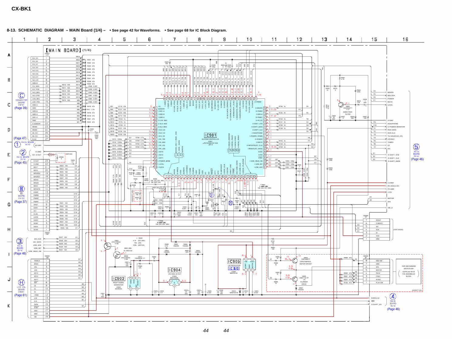
CX-BK1
4444
8-13. SCHEMATIC DIAGRAM – MAIN Board (1/4) – • See page 42 for Waveforms. • See page 68 for IC Block Diagram.
R910
R911
R912
R913
R914
R915
R901
R902
R903
R904
R905
R906
R907
R908
R916
R918
R919
R921
R922
R917
R909
C960
C959
C958
C961
C962
C963
R527
R528
R529
R530
R531
C939
C912
C919
C918
C917
C916
C915
C913
R719
R721
R722
R714
R725
R724
R726
R727
R728
R729
R702 C954
R920
R7
18
R7
17
R7
16
R7
12
R7
23
R7
13
R7
15
R7
11
R7
10
R7
09
R7
08
R7
07
R7
51
R7
41
R7
40
R7
30
R7
31
R6
39
R7
52
R7
34
R7
33
R7
38
R7
54
R7
32
R7
04
R7
03
R7
37
R952
R953
R969
D911 R968
C901
IC904
C932
R980
D904 R981
D906D902
C925
C952
C944C
91
0
C9
11
C909
C936
D905
C914D910C935C934C933
R745
R746
R744
R747
R748
R749
R753
R750
R739
C957
C956
C955
C920
C921
C9
08
C9
46
R761
R984
R961
R970R955
R958
R959
R960
C938
R967
CN901
CN905
R701
R9
40
R9
41
R9
42
Q906
C931
Q901
IC901µPD703260YGF-S04
C928
C9
30
C940
R982
R983
C949 R950
Q902
R923
R924
R925
R926
R927
R928
R929
R930
R931
R932
R933
R934
R935
R936
R937
R938
R939
C945
JR908
R943
R944
IC902
IC905
C943
R985
R987
R986
R988
D907
Q904
Q905
R989
R990
R991
R992
R763
CN903
CN902
C948
R945
R946
C9
05
C9
06
C9
51
C9
50
R957
X902
R9
98
R947
X9
01
R9
99
C926
R954
C927R951
C953
CN999
L901
C924
100
100
100
100
100
100
47k
47k
47k
47k
47k
47k
47k
47k
47k
47k
47k
47k
47k
2.2k
47k
0.001
0.001
0.001
0.001
0.001
0.001
100
100
100
100
100
0.1
1200p
1200p
1200p
1200p
0.0022
0.0022
1200p
10k
10k
10k
10k
1k
1k
1k
10k
10k
10k
R766
R764
R762
R760
2.7k
47k 0.0039
10k
10
k
10
k
10
k
1k
1k
1k
10
k
10
k
10
k
10
k
10
k
10
k
10
0
1k
1k
1k
2.2
k
1k
2.2
k
1k
1k
1k
1k
2.2
k
1k
1k
2.2
k
100k
100k
27k
1SS355TE-17 1k
10010V
M62703ML
0.1
4.7k
1SS355 470
1SS3551SS355
0.1
100p
0.001 18
p
22
p
1800p
10016V
1SS355
0.1MA8100-M0.02210016V
2225V
1k
1k
1k
1k
1k
1k
1k
1k
1k
100p
100p
100p
1
1
0.0
01
10
0p
10k
100
4.7k
01k
39k
1.5k
220k
150V
100
27P
19P
220k
2.7
k
15
0k
68
k
DTC144EKA-T146
1050V
DTA114EKA-T146
-JBT-A
2250V
0.0
01
100016V
100k
100k
100p 0
2SC3052F-T1-LF
100
100
100
100
100
100
100
100
100
100
100
100
100
100
100
100
100
0.1
0
0
10k
R520470k
BD4923G
MM1614A
0.001
1k
1k
1k
1k
1SS355
2SB1068TP
2SB1116-TP-LK
47k
47k
47k
47k
47k
8P
23P
100p
0
0.0
01
0.0
01
10
0p
10
0p
0
5MHz
4.7
M
1k
32
.76
8K
Hz
33
0k
0.001
10k
1050V10k
0.022
7P
0
0.22F50V
FR-GND
FR-VDD(3.3V)
V-STBY
SOL
MOTOR
O-SHIFT_DATA
O-SHIFT_CLK
O-SHIFT_STB
DO
CE
TUNED
STEREO
RDS-CLK
RDS-DATA
LEVEL
HEADPHONE
MUTE
POWER
MCLOCK
MDATA
D-GND
TU-SIG(ECHO_CE)
I2C_CLK
I2C_DATA
USB_ACK
USB_INT
USB_VBUS_ON
O-SHIFT_SO
O-POWER-MONITOR
CD_D-OUT
A-GND
M-GND
+12V
VM_D
EVER3.3V
M1
M2
M3
M6
M7
M8
M9
M10
M11
M12
M13
M14
M15
M16
M17
M18
M19
M20
M21
C1
P1
P2
P3
M5
M22
M23
A5
A6
A8
A9A2
A1
A7
F5
T5
M20
M18
M16
M14
M12
M10
M13
M17
M21
M23
M22
U3
U4
U5
A7
A5
A6
K1
K2
K3
K4
K5
K6
K7
K1
K2
K3
K4
K5
K6
K7
B1
B2
B3
B4
B5
B6
B2
B1
D3
D4
B3 S1
S2
S3
S1
S2
S3
U1
U2
U3
U4
U5
T1
T2
T3
T4
T5
T6
T7
S1
S2
S3
F4
F5
F6
F7
F9
A1
A2
F10
F6
F4
F7
F9
T1
T3
T4
T7
T6
S1
S2
S3
F8
F10
M19
M8
M6
M3
M1
M2
M5
M7
M9
M11
M15
B5
U1
U2
A8
A9
C20
C19
C18
C17
C16
C15
C14
C13
C12
C11
C10
C9
C8
C7
C6
C5
C4
C3
C2
B7
B7
C3
P3
P1
P2
F8
B6
B4
C5
C1
C9
C7
C14
C16
C18
C20
C19
C17
C15
C13
C8
C6
C4
C2
D2
D1
T2
C10
C11
C12
∗
I-SUFIX
AV
REF0
I-USB_ACK
I-D
EC
K_
PA
CK
O-MDATA
GND
VM
VDD
DATA
CLK
LCK
I-RMC
KEY1
KEY2
KEY3
DI
CL
CE
INH
JOG
VOL
TREBLE
BASS
GND
VDD
SI
SCK
SO
RESET
FLMDCO
I-SW2-B
I-SW1-A
I-D_
SENSOR
I-S
W3
I-USB_INT
STBY
STBY
O-M
P3
RS
T
O-PWM3
O-PWM2
D+5V
M+12V
M+12V
MGND
MGND
D.SENSOR
SW3
SW1-A
SW2-A
SW2-B
SW4
SW5-A
LOD_POS
LOD_NEG
SLD_POS
SLD_NEG
ELV_POS
ELV_NEG
SW5-B
SLD_E0
SLD_E1
SLD_E2
SLD_E3
ELV_E0
ELV_E1
ELV_E2
ELV_E3
SCOR
SQCK
SENS
SQSO
LDON
CLOK
XLT
DATA
XRST
PWM1
PWM2
PWM3
DGND
MP3STB
MIACK
MIDIO
MP3RST
MP3REQ
MICS
MILP
MICK
D-GND
D-OUT
GND
SOL
MOTOR
END SW
PACK
F.REC
R.REC
PLAY SW
O-L
CD
_C
LK
O-L
CD
_D
ATA
O-L
CD
_C
E
I-LE
V_
E2
I-E
LV
_E
3
I-E
LV
_E
1
I-S
LD
_E
3
BV
SS
BV
DD
I-S
LD
_E
1
O-E
LV
_P
OS
I-S
W2
-A
I-S
W4
O-L
OD
_P
OS
O-S
LD
_P
OS
I-S
W5
-B
O-D
ATA
I-C
LO
CK
I-S
QS
O(M
UT
E_
RE
Q)
I-S
QC
K(S
YS
_R
ES
ET
)
I-S
EN
S(4
CH
_C
LK
)
O-L
DO
N(4
CH
_D
ATA
1)
O-X
LT
(4C
H_
DA
TA
2)
O-X
RS
T
O-M
ICK
IO-M
IDIO
O-M
P3
RE
Q
O-M
ILP
O-SLD_NEG
O-LOD_NEG
O-ELV_NEG
I-SLD_E0
I-SLD_E2
I-ELV_E0
I-RE_VOL
I-RE_BAS
I-RE_TRE
I-RE_JOG
I-KEY1
I-KEY2
I-KEY3
I-POWER_MONI
I-LEVEL
I-SW5-A
I_R
DS
_D
ATAI_R
DS
_S
IG(E
CH
O_
CE
)A
VS
S
I-R
DS
_C
LK
AV
RE
F1
I-S
TE
RE
O
I-TU
NE
FL
MD
0
VD
D
RE
GC
VS
S
X1
X2
RE
SE
T
XT
1
XT
2
CA
N'T
US
E
I-D
EC
K_
PL
AY
SW
I-D
EC
K_
EN
DS
W
I-D
O
I-R
MC
I-S
CO
R
I2C
-US
B_
DA
TA
I2-U
SB
_C
LK
O-M
ICS
I-D
EC
K F
RE
C
I-D
EC
K_
RR
EC
I-USB_VBUS_ON
EVSS
EVDD
O-MUTE
O-POWER
I-HEADPHONE
O-SHIFT_CLK
O-SHIFT_DATA
O-SHIFT_STB
O-PLLCE
O-MCLK
I-POWER_DOWN
I-MIACK(I2C_DATA)
O-MP3STB(I2C_CLK)
O-PWM1
(1/4)
BAND-PASS
FILTER
SYSTEM CONTROLLER
(AEP,UK)
(EX
CE
PT
US
)
∗
(E51,MX)
(US)
(AEP,UK)
R945
4.7k
10k
150k
Q901,906
B+ SWITCH
VOLTAGE DETECT
GIO
RE
SE
T
NC
NC
GN
D
VD
D
RESET SIGNAL
GENERATOR
+4V REGULATOR
CO
NT
VIN VOUT
NO
ISE
GN
D
MOTOR DRIVER
CAPSTAN/REEL
DRIVE
PLUNGER
THE ASSEMBLED
BLOCK
SUPPLIED WITH
TAPE MECHANISM
DECK BLOCK
(FOR CHECK)
(EXCEPT US)
2.7k
2.7k
2.7k
R995
(AEP, UK)(US, E51, MX)
1M
R996∗
∗
C9231
C9220.1
(AEP, UK)
R9960 (AEP, UK)
10k (US, E51, MX)0 (AEP, UK)
R997∗
∗ R997(AEP, UK)
10k (US, E51, MX)0 (AEP, UK)
INH
10k
(Page 39)
(Page 47)
(Page 45)
(Page 37)
(Page 46)
(Page 61)
(Page 46)
(Page 46)

CX-BK1
4545
8-14. SCHEMATIC DIAGRAM – MAIN Board (2/4) –
Q604
Q607
Q605
C603
C604
C613
C602
C618
C637
C617
C6
23
C691
C601
C693
C503
C624
C501 C502
C519
C518
C638
C639
D611
D6
13
IC601
Q608
C653
C615
C614
C6
22
C6
34
C628
C6
32
C6
36
C656
C654
C655
C662
C6
31
C6
35
C661
C6
27
C6
25C
62
1
C6
33
C665
C517
C508
C507
C606
R640
R642
R644
R651
R652
R649
R648
R6
29
R6
65
R662
R664
R663
R603
R605
R606
R692
JR615
R514
R5
26
R525
R524
R523
R516
R521 R522
R517
R607
R509
R510
R616
R518
R694
R696
R670
R698
R699
R676
JR6
12
JR6
13
JR6
11
JR6
10
R604
R602
R647
R641
R643
R618
R626
R6
20
R622
R628
R623 R624
R6
19
R621
R625
R617
R601
R512
R695 R697
D501
JK603
JK602
C626
C611
R693
C619
R630
R675
R6
15
R6
13
JR617
IC604
C664
R671
C668 C669
CN004
CN504
JR607
IC501
R515
Q602
JR616
C504
R627
R614
JR624 C666
R610
C692
R5
11
C663R609
R645 C643
C657
JR614
C610
R674
2SD1306NE
2SD1306NE
2SC3052F-T1-LF
10016V
4.750V
4.750V
1050V
1050V
1025V
1050V
15
0V
4.750V
1050V
0.4750V
4.750V
150V
1050V
1050V
100 10V
100 10V
10025V
10025V
1SS355
1S
S3
55
M61529 FP
2SA1235TP
470p
0.001
0.001
0.0
22
0.0
22
0.0027
0.2
2
0.2
2
0.1
270p
270p
220p
0.2
2
0.2
2
220p
0.0
02
7
0.0
470.0
22
0.0
22
220p
0.1
0.1
0.1
0.1
2.2M
1.2k
47k
47k
0
4.7k
10
1M
0
18k
10k
22k
27k
27k
100
0
22k
10
0100
0
0
22k
0 0
100
0
10k
10k
0
100
2.7k
100k
100
5.6k
5.6k
2.2k
0 000
22k
4.7k
4.7k
2.2M
1.2k
2.2k
10k
1k
15k
22k
2.2k 2.2k
1k
15k
10k
2.2k
4.7k
22k
2.7k 100k
UDZSTE173.9B
1P
4P
0.047
4.750V
100
0.047
10k
2.2k
0
0
0
GP1FA313TZ
1050V
100
4716V
0.1
17P
5P
0
BU4052
22k
2SC3052F-T1-LF
0
4.750V
4.7k
0
0 220p
0
4.7 50V
22
k
1050V0
2.2k 4.750V
10016V
0
4.750V
100k
A1
A2
A3
A4
A5
A6
A7
A8
A9
A10
A11
B1
B2
B3
B4
B5
B6
B7
B8
B9
B1
0
D-GND
CD_D-OUT
O-M
DA
TA
O-M
CL
OC
K
LE
VE
L
RE
C-L
TA
PE
-L
TU
NE
R-L
REC-OUT-MUTE
USB_ON
USB_VBUS_ON
USB_INT
USB_ACK
I2C_DATA
I2C_CLK
I-MIC
LCK
B
A
REC-R
TAPE-R
TUNER-R
X1
X2
X3
X4
LCK
I-MIC
MIC-OUT
MIC-A-GND
VM
REF
MIC
CD
-R
TU
NER
-R
TA
PE
-R
REC
B-1
TM
I1
TM
O1
TC
A1
TC
B1
TC
C1
TO
UT1
VO
LIN
1
BB
-A1
BB
-B1
OU
T1
SA
OU
T
DA
TA
CL
OC
K
GN
D
SW
OU
T
OU
T2
BB
_B
2
BB
_A
2
VO
LIN
2
SU
R2/D
PL
2
SU
R1/D
PL
1
CD
-L
TU
NER
-L
TA
PE-L
REC
B-2
TM
I2
TM
O2
TC
A2
TC
B2
TC
C2
TO
UT2
VC
C
AU
X-L
AU
X-R
VSS
VEE
INH
Y1
Y3
Y2
Y0
COM Y
VDD
X2
X1
COM X
X0
X3
A
B
USB_ACK
VM
D-GND
USB-L
USB-R
V-GND
V-IN
A-GND
AUX2-L
AUX2-R
USB_ON
I2C_CLK
I2C_DATA
USB_INT
USB_VBUS_ON
D-GND
A-GND
(2/4)
(EX
CEP
T U
S)
LINE AMP
OPTICAL
OPTICAL
OUT
DIGITAL
(AEP,UK)
(E51,MX)
AUX AUDIO SELECTOR
MUTING
LINE AMP
MUTING
L
R
VIDEO OUT
AUX IN
L
R
AUX OUT
(E51,MX)
(US,AEP,UK)
(EXCEPT US)
INPUT SELECT/
ELECTRICAL
VOLUME
INVERTER
TRANSCEIVER
R51322k
R6500
C6940
2.2k
(Page 44)
(Page 51)
(Page49)
(Page 47)
(Page 46)
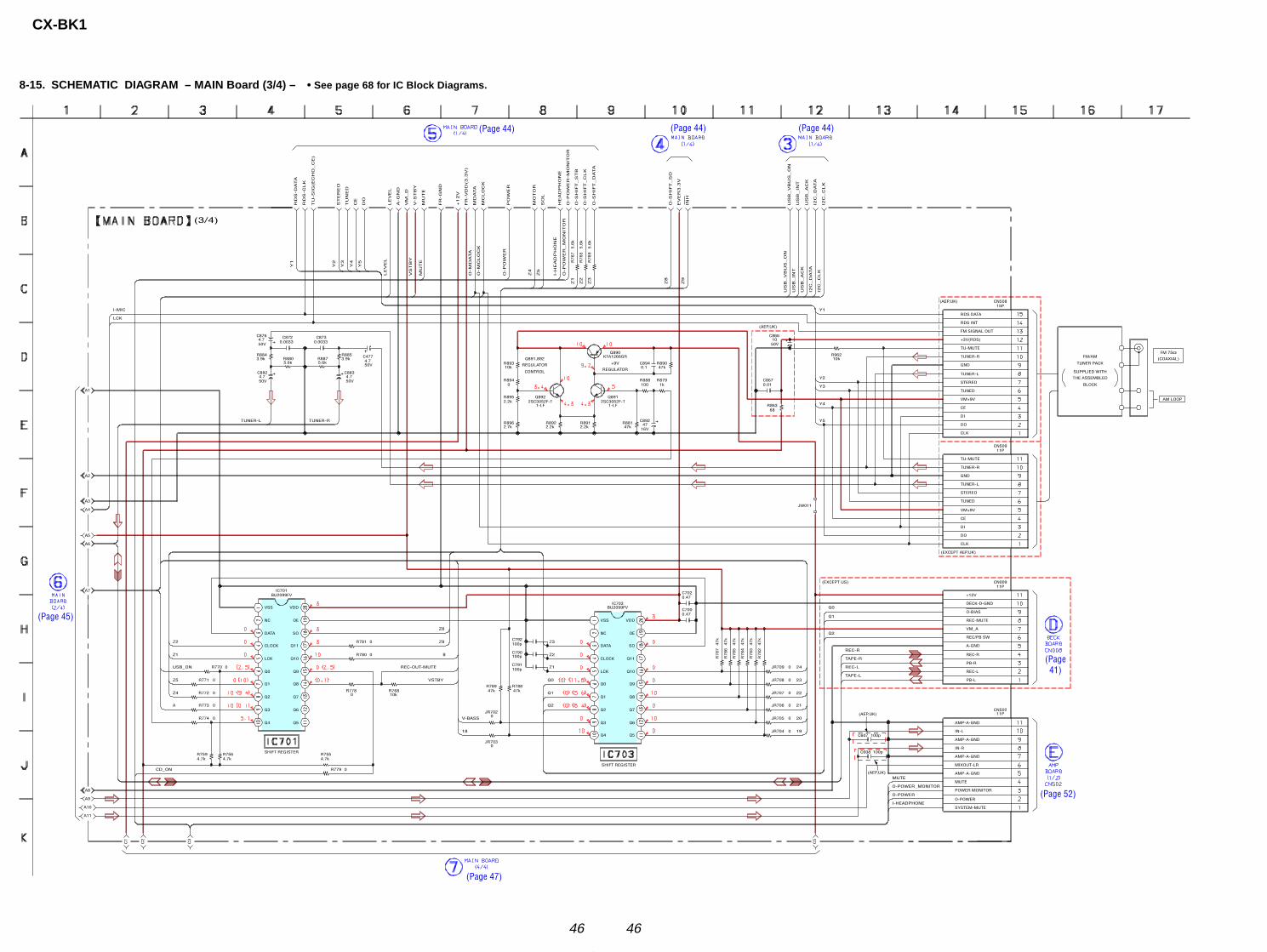
CX-BK1
4646
8-15. SCHEMATIC DIAGRAM – MAIN Board (3/4) – • See page 68 for IC Block Diagrams.
R884
C872 C873
R885
R895
R896
R894
R893
R892 R891
Q892 Q891
C894 R890
R888 R879
C892R881
JR708
JR709
JR707
JR706
JR705
JR704
R7
87
R7
86
R7
85
R7
84
R7
83
R7
82
C792
C790
C791
JR702
JR703
R780
R781
R770
R773
R774
R772
R771
C702
R755
R779
R7
67
R7
65
R7
69
R962
C876
CN502
C477
R788R789
CN009
CN509
CN508
Q890
C867
C866
R863
JW011
IC703
IC701
R778 R768
R756R759
3.9k R8805.6k
R8875.6k
0.0033 0.0033
3.9k
2.2k
2.7k
0
10k
2.2k 2.2k
2SC3052F-T1-LF
2SC3052F-T1-LF
0.1 47k
100 1k
4716V47k
0
0
0
0
0
0
47
k
47
k
47
k
47
k
47
k
47
k
100p
100p
100p
0
0
0
0
0
0
0
0
0
0.47
4.7k
0
5.6
k
5.6
k
5.6
k
10k
4.750V
4.750V
C8834.750V
11P
4.750V
47k47k
11P
11P
15P
KTA1266GR
0.01
1050V
68
BU2099FV
BU2099FV
0 10k
4.7k4.7k
A1
A2
A3
A4
A5
A6
A7
A8
A9
A10
A11
C1
C2
C3
C5
RD
S-D
ATA
RD
S-C
LK
ST
ER
EO
TU
NE
D
CE
DO
MU
TE
V-S
TB
Y
FR
-GN
D
FR
-VD
D(3
.3V
)
MD
ATA
MC
LO
CK
PO
WE
R
MO
TO
R
SO
L
LE
VE
L
HE
AD
PH
ON
E
O-P
OW
ER
-MO
NIT
OR
O-S
HIF
T_
SO
O-S
HIF
T_
ST
B
O-S
HIF
T_
CL
K
O-S
HIF
T_
DA
TA
US
B_
VB
US
_O
N
US
B_
INT
US
B_
AC
K
I2C
_D
ATA
I2C
_C
LK
EV
ER
3.3
V
TU
-SIG
(EC
HO
_C
E)
A-G
ND
+1
2V
VM
_D
19
20
21
22
23
24
O-P
OW
ER
_M
ON
ITO
R
I-H
EA
DP
HO
NE
O-P
OW
ER
CD_ON
I2C
_C
LK
I2C
_D
ATA
US
B_
AC
K
US
B_
INT
US
B_
VB
US
_O
N
O-M
CL
OC
K
O-M
DA
TA
LE
VE
L
Q0
Q1
Q2
18
V-BASS
VSTBY
REC-OUT-MUTE
B
Z1
Z2
Z3
Z1
Z2
Z3
Z1
Z2
Z4
Z5
Z8
Z9
A
USB_ON
Y1
Y2
Y3
Y4
Y5
Y1
Y2
Y3
Y4
Y5
TAPE-R
TAPE-L
Q0
Q1
Q2
REC-L
REC-R
MU
TE
TUNER-L TUNER-R
Z9
Z8
Z5
Z4
I-MIC
LCK
VS
TB
Y
CLK
DI
DO
CE
TUNED
TUNER-L
GND
TUNER-R
TU-MUTE
FM SIGNAL OUT
STEREO
+3V(RDS)
RDS INT
RDS DATA
VM+9V
CLK
DI
DO
CE
TUNED
TUNER-L
GND
TUNER-R
TU-MUTE
STEREO
VM+9V
A-GND
PB-L
REC-L
PB-R
REC-R
VM_A
REC/PB SW
REC-MUTE
DECK-D-GND
+12V
SYSTEM-MUTE
IN-R
AMP-A-GND
IN-L
O-POWER
AMP-A-GND
MUTE
POWER MONITOR
AMP-A-GND
AMP-A-GND
MIXOUT-LR
O-BIAS
Q5
Q8
Q9
Q10
Q11
SO
OE
VDD
Q6
Q7
Q5
Q8
Q9
Q10
Q11
SO
OE
VDD
Q6
Q7
VSS
DATA
CLOCK
LCK
Q0
Q1
Q2
Q3
Q4
VSS
DATA
CLOCK
Q0
Q1
Q2
Q3
Q4
LCK
(3/4)
(EXCEPT US)
THE ASSEMBLED
BLOCK
SUPPLIED WITH
FM/AM
TUNER PACK
AM LOOP
(COAXIAL)
FM 75Ω
(AEP,UK)
(EXCEPT AEP,UK)
+9V
REGULATORREGULATOR
Q891,892
CONTROL
(AEP,UK)
NC
NC
SHIFT REGISTER
SHIFT REGISTER
C882
INH
C7000.47
C607 100p
I-HEADPHONE
O-POWER_MONITOR
O-POWER
MUTE
C608 100p
(AEP,UK)
(AEP,UK)
(Page 45)
(Page 47)
(Page 52)
(Page41)
(Page 44)(Page 44)(Page 44)
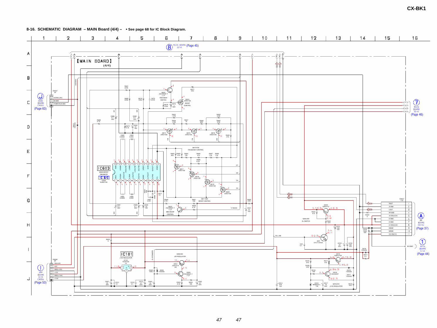
CX-BK1
4747
8-16. SCHEMATIC DIAGRAM – MAIN Board (4/4) – • See page 68 for IC Block Diagram.
Q616Q615Q614
Q617
Q618
Q619
Q620
C687 C629
C641
C640
C630C686
C007 C013 C050
C676
D6
12
D050
D018
C682 C684
C683 C685
C697
Q050
CN007
C696
C011 C012
C675
C677
R678
R677
R679
R681
R680
R658
R655
R688
R686
R683
R636
R657R656R689
R682 R684 R685 R687
R668
R667 R666
R672
R050
R052 R053
R011
R669
R6
35
CN006
Q051
Q623
IC603
Q624
Q625
CN507
C016
C20 C019 C018
R031
R032
Q024
Q019
R018
C014 C017D015
R017
Q018
D016
D017
R019
IC101
C052
R020
R003
R038
R016
C645
Q25
C015
2SK21582SK21582SK2158
2SK2158
2SK2158
2SK2158
2SK2158
4.750V
4.750V
4716V
4716V
4.750V
4.750V
2250V
4725V
1050V
150V
1S
S3
55
1SS355
1SS355
0.0033 0.033
0.0033 0.033
0.22
2SC3052F-T1-LF
4P
0.2
2
0.1 0.1
0.015
0.1
220k
22k
100k
220k
220k
820
4.7k
1.5k
8.2k
82k
27k
1k5.6k4.7k
47k 10k 47k 1.5k
4.7k
10k 270
4.7k
100k
8.2k 18k
2.2
4.7k
56
k
6P
2SA1015GR
2SC3052F-T1-LF
NJM2156
2SK2158
2SC3052F-T1-LF
11P
100016V
0.1 4725V
10010V
470
47k
2SB1013
2SB1370E
100
47016V
1050V
MA8033-LTW
47k
2SC3052F
1SS355
1SS355
470
TA7810S1A
4725V
0
0
220
470
2216V
DTC114YKA
10016V
B1
B2
B3
B4
B5
B6
B7
B8
B9
B1
0
C1
C2
C3
C5
M-GND
VS
TB
Y
21
22
23
24
V-BASS
O-P
OW
ER
X1
X2
X3
X4
18
19
20
CD_ON
ROUT
D-VDD(3.3V)
LOUT
CD-VM(7V)
D-GND
A-GND
A-VDD(3.3V)
MGND
MGND
D-GND
RF-GND
M-GND
+12V
VCC
+7.0V
GND(+12V)
GND(+7.0V)
VM+9.0V
GN
D
GO
UT
GIN
VR
EF
OU
TB
LO
UT
B
LIN
B
HO
UT
B
HIN
B
INB
HO
UT
A
HIN
A
INA
LIN
A
LO
UT
A
OU
TA
BB
E
LP
OU
T
LP
IN
V+
(4/4)
VSTBY(+9V)
TUNER/AUX GND
GI O
+10V REGULATOR
Q050,051
+9V REGULATOR
BBE ON/OFF
CONTROL
BASS BOOST
ENHANCER
Q617-620
BOOST CONTROL
FREQUENCY CONTROL
Q614-616
CONTROL
BOOST
FEED BACK
SWITCH
Q024,025
B+ SWITCH
Q018,019
+3.3V REGULATOR
R6603.3k
R6592.2k
(Page 53)
(Page 63)
(Page 45)
(Page 46)
(Page 37)
(Page 44)

CX-BK1
4848
8-17. PRINTED WIRING BOARD – USB AUX Board – • See page 35 for Circuit Boards Location. :Uses unleaded solder.
JW70
5
JW70
6
JW70
7JW70
8
JW70
9
JW71
0
JW71
1
JW71
2
JW71
3
JW714
JW715
JW716
JW717
JW718JW719
JW720 JW721JW722
C717
C756
CN701
X700
CLP701
IC701
C713
EP701
C716
C759
C758
JW70
0
EP702
C715
JW724
JW723
JW72
5
JW70
4
JW70
2
JW703
R727
L705L702L701
L700
C704
C703
R702
R703
C711
C762
C760
C757
R728
R724
L703
Q701
R722
Q700
C721
R712
C709
Q702
R729
R730
R732
R710
C708R720R718
R723
R700R701
R726
R725
C720
C718C722
C719
R721
R716
C712
C701C700
C710
IC700R706
R705
R711
C705
R707 C702
R704
C755C714
R731
JR70
1
R735
R736
JR702JR703
C724
C725
C706
EP702
J701
1
E
E
E
3
1 44
22
12
11
33
34
23
(CHASSIS)
R
L
AUDIO
VIDEO
LINE IN
1-688-415-
13
(13)
(USB)
2 3
1 4(FRONT VIEW)
(CHASSIS)MAIN BOARDCN004G
USB AUX BOARD
(Page 43)
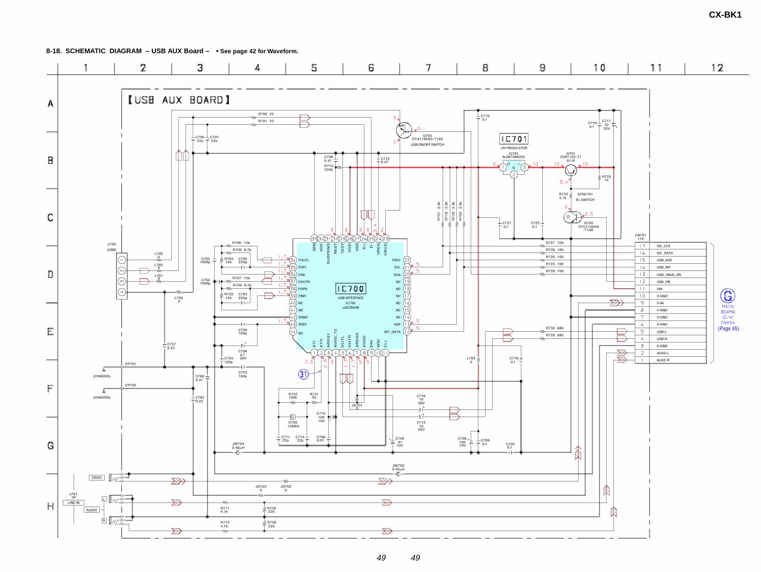
CX-BK1
4949
8-18. SCHEMATIC DIAGRAM – USB AUX Board – • See page 42 for Waveform.
R727
R726
R728
R724
R725
C718
R735
R736
R711
R712
R729
R730
C725
C724
C756
C755
C760
C762
R702 C704
R707
R704
C702
C703 R703 C705
R706
R705
C701C700
R700
R701
C759 C709C758
C721 C722
R7
21
R7
16
R7
18
R7
20
R722
R723
C717C719
Q701IC701C708
R710
C712
IC700
C710
C720
C714
X700
C711
R732
C715
C706
R731 C716
C713
C757
EP701
EP702
CN701
J700
L705
L702
L701
L700
Q702
L703
JW702
JW704
JR702JR703
Q700
J701
100
100
100
100
100
0.1
22k
22k
4.7k
4.7k
680
680
100p
100p
4.750V
100p
0.47
0.22
15k 220p
15k
8.2k1000p
1000p 15k 220p
15k
8.2k
22p22p
22
22
4710V 0.1100
10V
0.1 0.1
3.3
k
3.3
k
3.3
k
3.3
k
4.7k
1k
3325V0.1
2SB1132-T101-R
NJM78M05S0.47
220k
0.47
0.1
0.1
22p
12MHz
22p
100k
10010V
0.01
33 1050V
1050V
0.22
17P
0
DTA114EKA-T146
0
00
DTC114EKA-T146
3P
SO
F
SU
SP
EN
D
TES
T
FOUTL
FOPL
FINL
FOUTR
FOPR
FINR
NC
NC
SGND
SREF
NC
SEN
RES
T
VD
D
VS
S
D+
D-
VR
EG
VB
US
TRDY
SCL
SDA
NC
NC
NC
NC
NC
NC
ACK
INT_DATA
CL
I
WS
I
DA
I
AV
DD
AR
EG
0
OU
TR
OU
TL
AV
SS
_12
AR
EG
1
XT
O
XT
I
(CHASSIS)
(CHASSIS)
A-GND
USB-L
USB-R
A-GND
AUX2-L
AUX2-R
USB_ACK
VM
D-GND
V-GND
V-IN
USB_ON
I2C_CLK
I2C_DATA
USB_INT
USB_VBUS_ON
D-GND
(USB)
USB ON/OFF SWITCH
USB INTERFACE
µAC3553B
+5V REGULATOR
GIO
B+ SWITCH
Q700,701
L
R
AUDIO
VIDEO
LINE IN
0
0
0
0.45µH
0.45µH
JR7010
(Page 45)
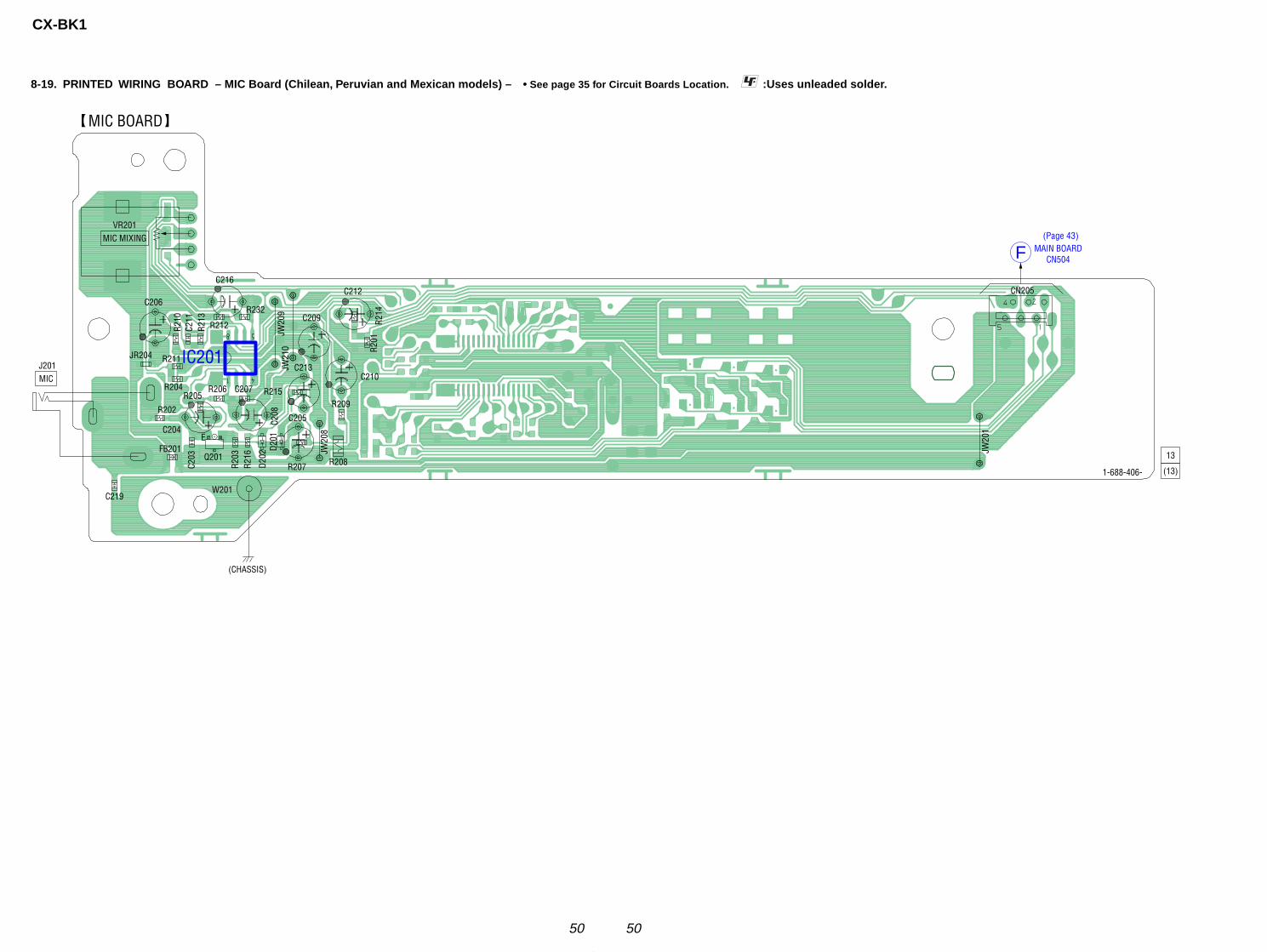
CX-BK1
5050
8-19. PRINTED WIRING BOARD – MIC Board (Chilean, Peruvian and Mexican models) – • See page 35 for Circuit Boards Location. :Uses unleaded solder.
C216
C209
C206
C204
C208 C205
C210
C212
VR201
JW20
1
J201
CN205JW
209
JW21
0
JW20
8
C213
W201
Q201
R203
R211
R210
R204
R232
R212R213
C211
R202
C203
R205R206 C207
C219
D201
D202
R207
R209
R208
R201
R214
IC201
FB201
R215
R216
JR204
1-688-406-
13
(13)
MIC BOARD
MIC
MIC MIXING
(CHASSIS)
MAIN BOARDCN504F
E
(Page 43)
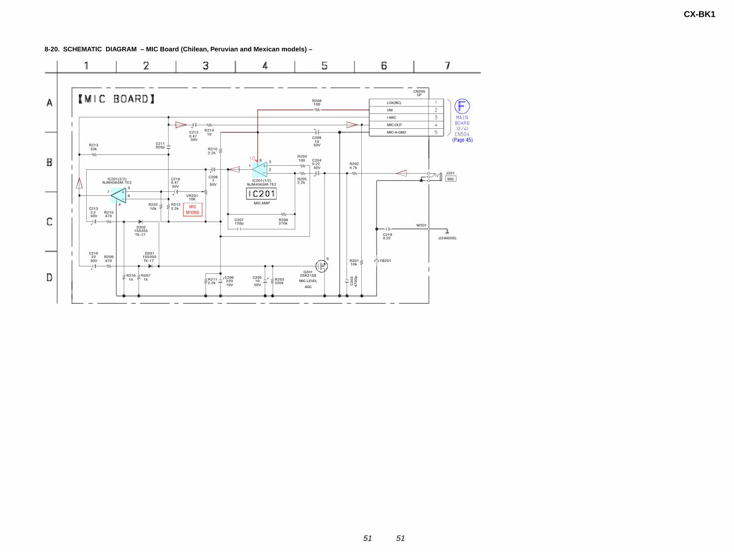
CX-BK1
5151
8-20. SCHEMATIC DIAGRAM – MIC Board (Chilean, Peruvian and Mexican models) –
CN205
W201
C219
FB201R201
R216 R207R211 C206 C205 R203
D201
R206
R204C204
R202
IC201(1/2)
Q201
C216
R215C213
C210R209
R213R210
C211
R212R232
VR201
C209
R205C208
C207
C2
03
R208
C212 R214
J201
IC201(2/2)
5P
0.22
10k
1k 1k2.2k 220
10V1050V 220k
1SS355TE-17
270k
1000.2250V 4.7k
NJM4565M-TE2
2SK2158
0.4750V
4702.250V
2250V 470
33k2.2k
820p
2.2k10k
10K
1050V
2.2k150V
120p
47
00
p
100
0.4750V
10
NJM4565M-TE2
I-MIC
MIC-OUT
MIC-A-GND
VM
LCK(NC)
(CHASSIS)
MIC AMP
AGC
MIC LEVEL
S
MIC
8 3
21
4
6
57
D2021SS355TE-17
MICMIXING
(Page 45)
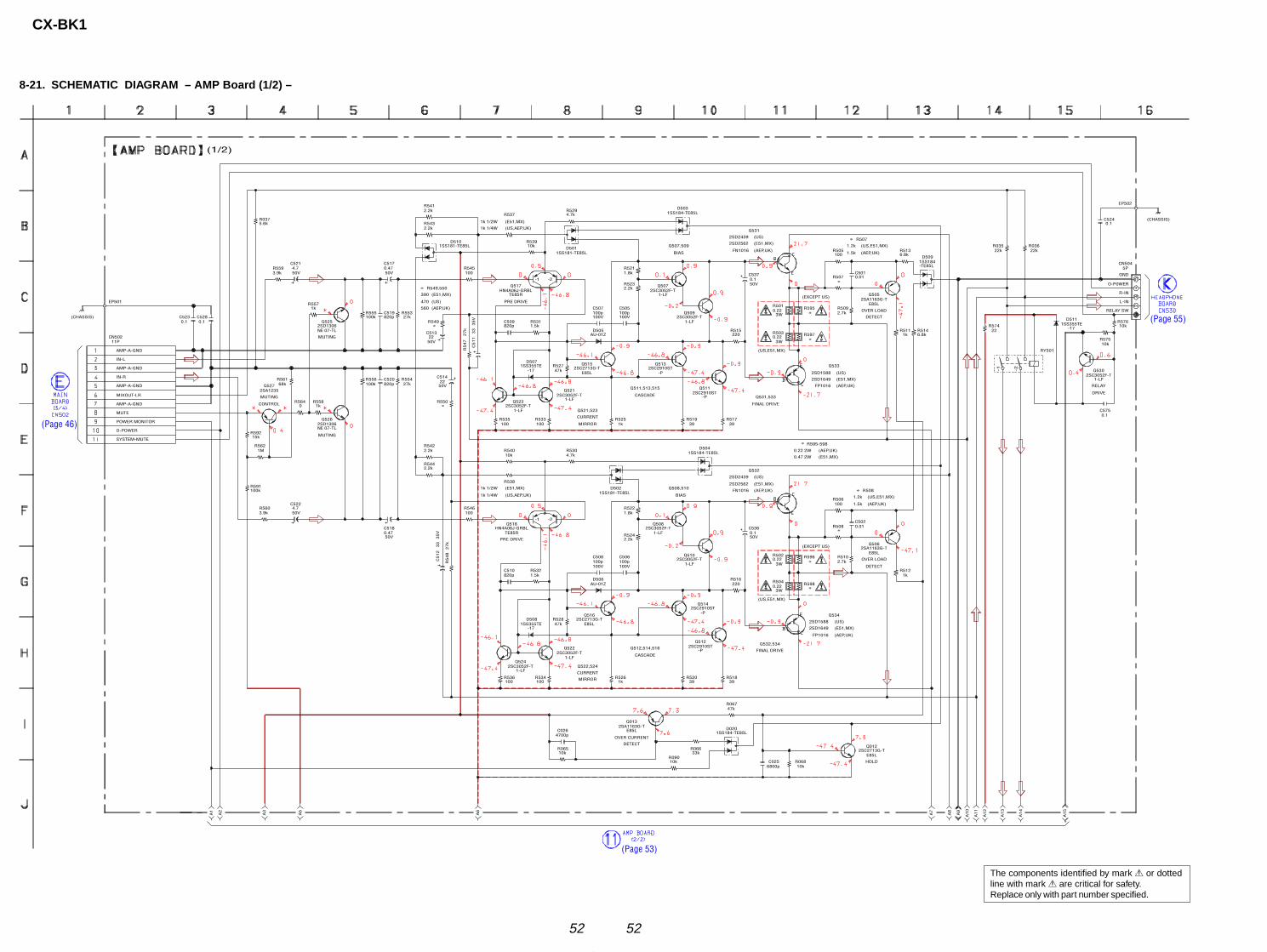
CX-BK1
5252
8-21. SCHEMATIC DIAGRAM – AMP Board (1/2) –
CN502
R505
R511
R035 R036
C524
R574
D511
R509
C537
Q507
Q509
R515
C507 C505
D505
R519
R521
R523
Q515R527
R517R525
D507
R535
Q523
Q521
R531C509
R541
R543
R539
R545
Q517
D501
D503R529
R533
R553C519R555
Q525
R557
R559C521 C517
D510
EP501
R547
C511
R513
R514
R506
C502
R510
Q506
R512
C508 C506
R516
R532C510
R530
D502
R522
R524
Q516
D506
R528
Q522
R536 R534
C536Q508
R526 R520 R518
R540
R546
R544
R542R
548
C512
C514R554C520R556
C522R560
R558
Q526
R561
R562
R592
R037
R591
D020
R067
R066
C026
R065 Q012
R068C025R090
D509
EP502
C518
D504
Q505
C523 C528
CN504
R575
R576
RY501
C575
R564
Q527
R550
R549
C513 R503
R501
R597
R595
R507
Q531
C501
Q533
R537
R538
R596
R598R504
R502
Q534
Q532
R508
Q013
D508
Q518
Q530
Q524
Q514
Q512
Q510
Q511
Q513
11P
100
1k
22k 22k
0.1
22
1SS355TE-17
2.7k
0.150V
2SC3052F-T1-LF
2SC3052F-T1-LF
220
100p100V
100p100V
AU-01Z
39
1.8k
2.2k
2SC2713G-TE85L47k
391k
1SS355TE-17
100
2SC3052F-T1-LF
2SC3052F-T1-LF
1.5k820p
2.2k
2.2k
10k
100
HN4A06J-GRBLTE85R
1SS181-TE85L
1SS184-TE85L4.7k
100
27k820p100k
2SD1306NE 07-TL
1k
3.9k4.750V
0.4750V
1SS181-TE85L
27k
33
35V
6.8k
6.8k
100
0.01
2.7k
2SA1163G-TE85L
1k
100p100V
100p100V
220
1.5k820p
4.7k
1SS181-TE85L
1.8k
2.2k
2SC2713G-TE85L
AU-01Z
47k
2SC3052F-T1-LF
100 100
0.150V
2SC3052F-T1-LF
1k 39 39
10k
100
2.2k
2.2k27k
33
35V
2250V27k820p100k
4.750V3.9k
1k
2SD1306NE 07-TL
68k
1M
15k
5.6k
100k
1SS184-TE85L
47k
33k
4700p
10k 2SC2713G-TE85L
10k6800p10k
1SS184-TE85L
0.4750V
1SS184-TE85L
2SA1163G-TE85L
0.1 0.1
5P
10k
10k
0.1
0
2SA1235
2250V
0.223W
0.223W
0.01
0.223W
0.223W
2SA1163G-TE85L
1SS355TE-17
HN4A06J-GRBLTE85R
2SC3052F-T1-LF
2SC3052F-T1-LF
2SC2910ST-P
2SC2910ST-P
2SC3052F-T1-LF
2SC2910ST-P
2SC2910ST-P
A1
A2
A3
A5
A6
A7
A8
A9
A10
A11
A12
A13
A14
A15
∗
∗
∗
∗
∗
∗
∗
∗
(CHASSIS)
L-IN
R-IN
GND
O-P0WER
RELAY SW
IN-R
AMP-A-GND
IN-L
O-POWER
AMP-A-GND
MUTE
POWER MONITOR
AMP-A-GND
AMP-A-GND
SYSTEM-MUTE
MIXOUT-LR
(1/2)
(CHASSIS)
-1 -2
MUTING
MUTING
CONTROL
MUTING
∗(E51,MX)
(US)
(AEP,UK)
R549,550
470
390
560
PRE DRIVE
-2-1
CASCADE
Q511,513,515
Q521,523
CURRENT
MIRROR
Q531,533
FINAL DRIVE
(US,E51,MX)
(EXCEPT US)
(E51,MX)
(US)
(AEP,UK)
2SD2439
2SD2562
FN1016
∗
(AEP,UK)
R507
1.2k
1.5k
(US,E51,MX)
OVER LOAD
DETECT
(E51,MX)
(US)
(AEP,UK)
2SD1588
2SD1649
Q507,509
BIAS
(E51,MX)1k 1/2W
1k 1/4W (US,AEP,UK)
(E51,MX)1k 1/2W
1k 1/4W (US,AEP,UK)
PRE DRIVE
-2-1
BIAS
Q508,510
(EXCEPT US)
(US,E51,MX)
(E51,MX)
(US)
(AEP,UK)
2SD1588
2SD1649
FINAL DRIVE
Q532,534
(E51,MX)
(US)
(AEP,UK)
2SD2439
2SD2562
FN1016 ∗
(AEP,UK)
1.2k
1.5k
(US,E51,MX)
R508
∗
(AEP,UK)
R595-598
0.22 2W
0.47 2W (E51,MX)
OVER LOAD
DETECT
CASCADE
Q512,514,516
CURRENT
MIRROR
Q522,524
DETECT
OVER CURRENT
HOLD
DRIVE
RELAYFP1016
FP1016
(Page 55)
(Page 53)
(Page 46)
The components identified by mark 0 or dottedline with mark 0 are critical for safety.Replace only with part number specified.

CX-BK1
5353
8-22. SCHEMATIC DIAGRAM – AMP Board (2/2) –
R651
R6
45
R6
46
TH502
TH501
R648R649
D6
18
D6
19
Q610
R650
Q611
R652
R6
47
R664
C645
R6
27
R626
R663
R661 C631
D632
D637
R653
R669C640
C630
D638
Q624
C643
R670
R675R659
Q623C642
Q622
D635
D634
R671
D633R679
R672
C634
Q617
R674
R678R658
D627
R660
D636
R677
C641
R662
R694
D631R676
R685R691
Q621C638
R682
Q620
D629
D630
C637
C636
D624
D625
C635
C633
R683
D626
C008
C009
C007C005
IC003
D002
C002 C003C004 C001
CN003
IC001
CN601
D301
R311 R312
JW016
R303
R307 Q303
Q302
R306
R305 Q301
R304
C303
C302
R302R301
C301
CN303
M301
JW023
R641R643
R6
42
R698R696 R697
D623
R695R681
R699
R692 R693
Q618
JW601
Q619
JW602
JW0
12
JW017
JW013
JW042JW041
CN006
CN004
JW014
R654
R655
R656
R686
2.2k
47
k
47
k
220k220k
1S
S1
84
-TE
85
L
1S
S1
81
-TE8
5L
2SA1163G-TE85L
10k
DTA114EKA-T146
47k
22
k
3.3k
330p
10
k
3.3k
10k
3.3k 330p
1SS355TE-17
1SS355TE-17
3.3k
10k330p
330p
1SS355TE-17
2SA1235
330p
15k
2.2k270
2SA123522p
2SB792A(RS)
1SS355TE-17
1SS355TE-17
10k
1SS355TE-175.6k
4.7k
4763V
2SA1235
47k
33k330
FMB-G16L
2.7k
1SS355TE-17
3.3k
4735V
10k
10k
1SS355TE-172.7k
2.2k120
2SC3052F-T1-LF330p
15k
2SD814A(RS)
1SS355TE-17
UDZSTE1715B
4763V
100p
1SS355TE-17
MA8180
0.068
4735V
4.7k
FMB-G16L
0.1
4725V
0.12250V
TA7812S
1SS355
0.1 4725V
2250V 0.1
4P
TA7807S
4P
1SS184
4.7k 4.7k
3.3k
3.9 2SA1015GR
2SA1235F
10k
10k 2SC3052F
220
4725V
4725V
470k47k
150V
3P
22k
15k
1SS355TE-17
22k15k1/2W
3.3k
3.3k 3.3k
2SK3053
2SK3053
6P
13P
15k
1.5k
1.8k
3.3k
A1
A2
A3
A5
A6
A7
A8
A9
A1
0
A1
1
A1
2
A1
3
A1
4
A1
5
∗ ∗
∗ ∗
FR SP GND(R)
FR SP GND(L)
VH+
VH-
VL+
VL-
RELAY GND
O-POWER
POWER-MONITOR
VM+9V
DC-DET
SP-GND
SP-GND
FAMP-A-GND
REG
REG-GND(+7V)
REG-GND(+4V)
REG-GND(+12V)
+12V
+7.0V
GND(+12V)
GND(+7.0V)
VM+9.0V
VCC
(2/2)
FR SP OUT(R)
FR SP OUT(L)
(FAN)
Q301-303
FAN MOTOR DRIVE
+12V REGULATOR
GOI
THERMAL DETECT
Q610,611∗
1.8k
2.2k
(E51,MX)
(US,AEP,UK)
R642,643
∗(E51,MX)
(US,AEP,UK)
R697,698
1.5k
1.8k
Q620,621
OUTPUT LEVEL
DETECT
SWITCHING
SWITCHING
OUTPUT LEVEL
DETECT
Q617,622-624
(EX
CE
PT
US
)
GOI
+7V REGULATOR
(US)
(Page 63)
(Page 47)
(Page 63)
(Page 52)
(Page 57)

CX-BK1
5454
8-23. PRINTED WIRING BOARD – AMP Board – • See page 35 for Circuit Boards Location. :Uses unleaded solder.
Ref. No. Location Ref. No. Location Ref. No. Location Ref. No. Location
• Semiconductor Location
JW511
JW515
JW51
6
JW51
7
JW519
JW520
JW521
JW52
3
JW52
4
JW526
JW52
8
JW52
9
JW53
0
JW53
1
JW53
2
JW53
3
JW53
4
JW53
5
JW53
6
JW53
7
JW538
JW020
JW022
JW02
4
JW025
JW027
JW029
JW030
JW031
JW034
JW03
5
JW61
2
JW61
3
JW61
4
JW615
JW616
JW618
JW61
9
JW03
6
JW518
JW514
JW522
JW02
8
JW540
JW541
JW54
2
JW543
JW544
JW021
JW038
JW539
JW033
JW032
C003
EP502 EP501
R597R501 R503
CN504
R596 R502
R595
Q531 Q533
Q513
R598R504
C009
C536
C517C514
C518
C521
C537
C522
C512C511
JW02
3
CN004
CN006
C513
JW01
4
RY501
Q511
D505
CN502
JW013
CN003
JW012
D626
C633
JW60
1
D627
C641C634
C637
C301
C302
Q303
C303
IC003
IC001
JW01
6
JW602
Q532
Q534
Q514
Q512
D506
Q619 Q618
R537
JW03
7
JW527
R538
JW512
JW513
R655
R656
R695R6
86 R699
R692
R693
JW611
CN601
C004
C005
CN303
JW041
JW042
JW52
5
R681
JW545
JR514
JR515
JR11
17
JR11
16
JR11
15
JR11
14
JR11
13
JR512
JR513
R090
JR511
JR517
C635
Q507 Q509
TH501 C001C002
C007
C008
C025
C026
C501
C505
C506
C507
C508
C509 C510
C519 C520
C523
C528
C575
C630
C631
C638
C640
C642
C643
C645
D020
D501 D502
D503
D504
D507
D509
D511
D618 D619
D623
D624
D629
D631
D632
D633
D634
D635
D636
D637
D638
Q611
R065
R066
R067 R068
R505
R506
R507
R508
R509
R510
R311
R312
R513R514
R515R516
R517 R518R519 R520
R521 R522
R523 R524
R525 R526R527 R528
R529 R530R531 R532
R533 R534
R535 R536R539
R540
R541R542
R543R544
R545 R546
R547R548
R551
R553 R554
R555 R556
R557 R558
R559
R560R561
R562
R574
R575
R576
R591
R592
R627
R697
R643
R645
R646
R647
R648
R649
R650
R651
R652
R698
R654
R659
R660
R653
R662
R663
R626
R669
R670
R671
R672
R674
R675
R676
R677
R679
R682
R685R691
R694
R696
R642
Q515
Q521
Q523Q517
D630
D625
Q624
Q623
Q622
Q621
R511
Q620
Q617
Q525
R664
R658
R661
R641
R036
D301
R301
R302 Q301
R303
R305
R306
Q302R307
Q530
D508
Q508 Q510
TH502
Q012
D510
Q516
Q522
Q524Q518
R512
Q526
Q506
R035
Q527
Q013
Q610
R037
C524
R549 R550
D002
R564
C502
R304
Q505
JR11
30
C636
JW617R678
R683
JW017
AMP BOARD
1-688-420-
11
(11)
(US) (E51) (MX) (UK)
(AEP)
13
(CHASSIS)
13
1
1 6
4
EMAIN
BOARDCN502
IMAIN
BOARDCN006
1
2
3 M301(FAN)
M
E
EE
E
E
N ACDC BOARDCN006
(US)
E
E
EE
E1B 2B
1C 2CE
E
E A
KK
K
AAA
KKA
KK
A
KK K
AA
K
AA
(US,
E51
, MX)
(US,
E51
, MX)
(US,
E51
, MX)
(US, E51, MX)
(EXC
EPT
US)
(EXCEPT US)
(EXC
EPT
US)
(EXC
EPT
US)
E
E
E
E
E
EE
E
E
E
E
E
E
E
E
E
E
1B 2B
2C1C
E
(EXCEPT US)
DG SDG S
E
EE
E
K
A A
K
AA
K
AA
114 5
-1
-2
M ACDC BOARDCN003
KHEADPHONE
BOARDCN530
LSPEAKERBOARDCN503
(CHASSIS)
1 2 3 4 5 6 7 8 9 10 11 12 13 14 15 16 17 18
A
B
C
D
E
F
G
H
I
J
K
113
D002 I-14D020 B-3D301 F-3D501 D-6D502 D-11D503 C-6D504 D-11
D505 D-5D506 D-9D507 C-5D508 C-9D509 D-3D510 C-11D511 F-2
D618 E-7D619 E-8D623 I-11D624 H-8D625 H-9D626 G-9D627 G-7
D629 I-11D630 J-11D631 G-11D632 G-11D633 G-9D634 H-9D635 H-9
Ref. No. Location Ref. No. Location Ref. No. Location Ref. No. Location Ref. No. Location Ref. No. Location Ref. No. Location
D636 H-10D637 G-10D638 G-10
IC001 E-13IC003 E-17
Q012 B-3Q013 C-2Q301 J-14Q302 J-14Q303 J-15Q505 E-3Q506 D-8
Q507 E-5Q508 E-9Q509 E-5Q510 E-9Q511 D-5Q512 D-10Q513 D-6
Q514 D-10Q515 D-5Q516 D-9Q517 C-5Q518 C-10Q521 C-4Q522 C-9
Q523 C-4Q524 C-9Q525 C-4Q526 C-8Q527 B-11Q530 G-2Q531 E-4
Q532 E-9Q533 E-6Q534 E-11Q610 D-4Q611 E-4Q617 H-6Q618 H-8
Q619 H-6Q620 H-11Q621 I-12Q622 G-9Q623 G-10Q624 H-11
(Page 56) (Page 55)
(Page 62) (Page 62)
(Page 43)
(Page 43)

CX-BK1
5555
8-24. PRINTED WIRING BOARD – HEADPHONE Board – • See page 35 for Circuit Boards Location.
:Uses unleaded solder.
8-25. SCHEMATIC DIAGRAM – HEADPHONE Board –
JW524
R523
R526 R524
J521JW523
R525
CN53
0
W505
JR501
C521
C550
R521
R522
HEADPHONE BOARD
1-688-414-11
(11)
PHONES
1
5
AMPBOARDCN504
K
(CHASSIS)
(Page 54)
R521 C550
R524R526
R525 R523
JW523
W505
J521
R522
CN530
2.2k 0.22
2701/2W
2701/2W
2701/2W
2701/2W
2.2k
5P
(CHASSIS)
L-IN
R-IN
GND
O-P0WER
RELAY SW
PHONES
(Page 52)
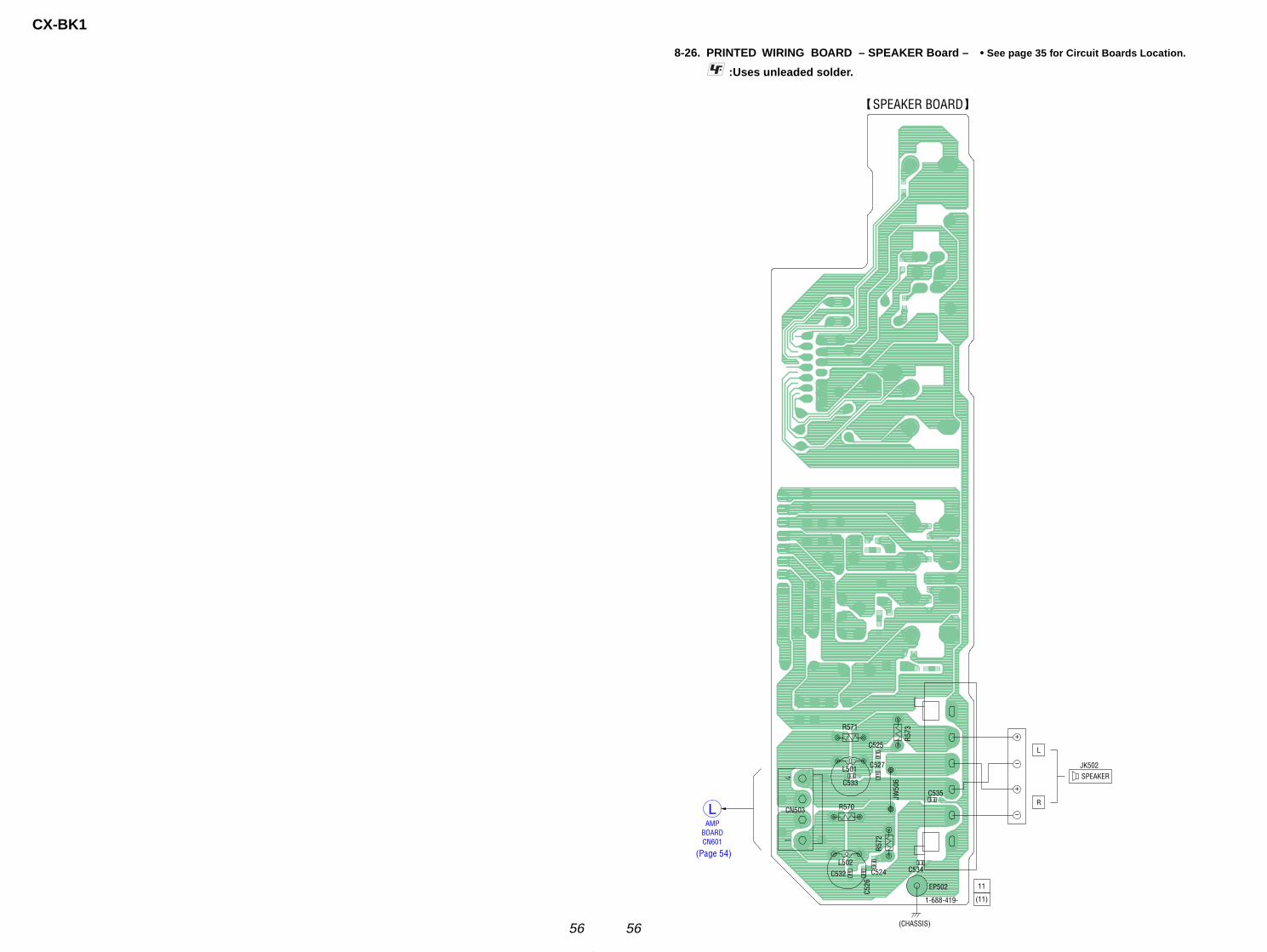
CX-BK1
5656
8-26. PRINTED WIRING BOARD – SPEAKER Board – • See page 35 for Circuit Boards Location.
:Uses unleaded solder.
JW50
6
R571
JK502L501
L502
R573
R572
R570CN503
EP502
C535
C534C524C5
26C532
C533
C527
C525
SPEAKER BOARD
1-688-419-
11
(11)
+
–
L
R
SPEAKER
–
+
(CHASSIS)
AMPBOARDCN601
L
(Page 54)
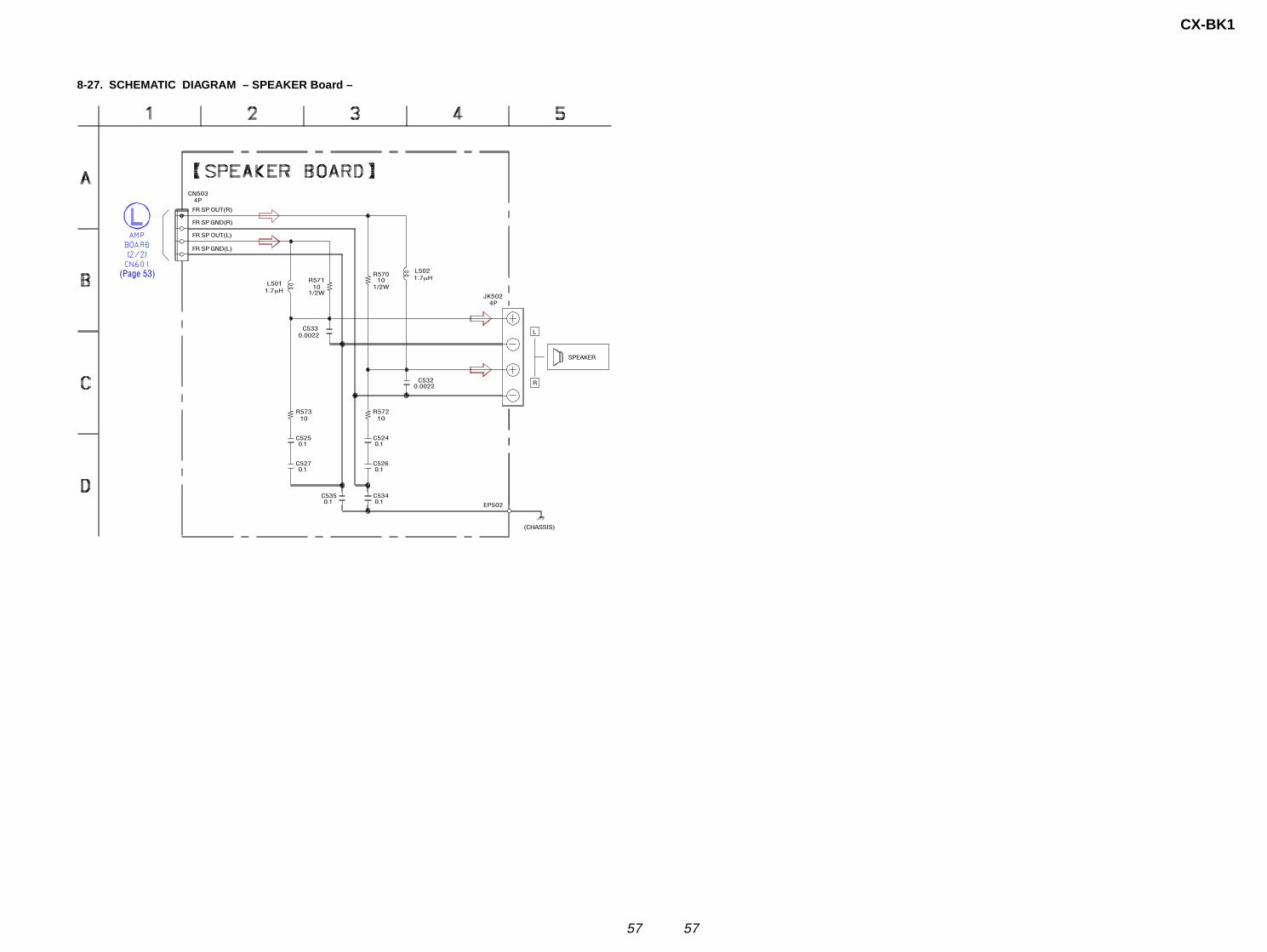
CX-BK1
5757
8-27. SCHEMATIC DIAGRAM – SPEAKER Board –
CN503
L502R570R571
C533
L5011.7µH
1.7µH
C525
R573
C527
R572
C524
C526
C534C535
C532
JK502
EP502
4P
101/2W10
1/2W
0.0022
0.1
10
0.1
10
0.1
0.1
0.10.1
0.0022
4P
FR SP GND(R)
FR SP GND(L)
FR SP OUT(R)
FR SP OUT(L)
(CHASSIS)
L
R
SPEAKER
(Page 53)
CX-BK1
5858
JW60
1
JW60
2
JW60
6
JW60
9
JW610
JW61
1
JW61
2
JW61
3
JW614
JW615
JW616
JW617
JW618
JW619
JW620
JW62
5
JW626
JW62
7
JW629
IC603
S316
S311S312
S313
S315
S314
S331
S333
S320 S318
S334
S332
S317
S319
LED634
C607
LED635
LED631
LED633
LED632
CN606
CN612
JW60
5
JW62
4JW628
JW623
JW608
JW60
3
JW60
4
JW622
JW621
CN605
JR60
1
JR602
JR604
JR605
JR606
JR607
JR608
JR609
JR610
JR603
B3
R608
Q601
Q604
Q602
Q605
R624
R626
R625
R623
R622
R607
R330
R310
R320
R319R318
R334R333
R332
R331
R317
R316
R616
R315
R314
R313
R312
R311
R620
R617
R621
R619
R618
R604
R605
R606
C606
C604
C605
C621
R611
C601
IC601
IC602
C602
C603
R601
R602
R603
JR611
Q603
C608
C609
S335
S336
S337
S338
S339
LED202
LED203
CN607
R335R336
R337
R338
R339
R345
R346
LED601CN613
20
11
1
10
1-688-411-
13
(13)
KEY LED RMC BOARD
1-688-407-
13
(13)
LEFT BUTTON BOARD
LED BOARD
1-688-412-
13
(13)DISC SLOT
ILLUMINATION
LED601
1 2
1 2
1
5
1
5
LCD VOLBOARDCN004
P
STANDBY/ON
POWER
FUNCTION
BAND
GEQ
i-BassLED203, S339
TUNING DOWNUP
ALBUM/PLAY LIST
S311 − 320,S331 − 339
1
10
20
11
PLAY MODE
2
1
5
3
4
EJECT
1B
2B2C
1CE
2C
1C 1BE
2B
2C
1C 1BE
2B
2C
1C 1BE
2B
2C
1C 1BE
2B
DISCINDICATOR
1
DISCINDICATOR
3
DISCINDICATOR
2
DISCINDICATOR
4
LED634
DISCINDICATOR
5
LED635
DISC SELECT5
S315
DISC SELECT4
S314
DISC SELECT 3
DISC SELECT 2 DISC SELECT 1
A
B
C
D
E
F
1 2 3 4 5 6 7
PRESET PRESET STOP/CLEAR PAUSE/SET
(US)
(Except US)
REC
(US)
(Except US)
8-28. PRINTED WIRING BOARDS – KEY Section – • See page 35 for Circuit Boards Location. :Uses unleaded solder.
IC601 B-4IC602 D-3IC603 C-5
LED202 A-7LED203 E-7LED601 F-1LED631 D-3LED632 E-3LED633 E-3LED634 D-2LED635 E-2
Q601 D-4Q602 E-4Q603 E-3Q604 D-2Q605 E-3
• SemiconductorLocation
Ref. No. Location
(Page 60)
CX-BK1
5959
8-29. SCHEMATIC DIAGRAM – KEY Section – • See page 42 for Waveform.
R346
R335 R336 R337 R338 R339
S339S338S337S336S335
R330
R310
R331 R332 R333 R334
S334S333S332S331
S311 S312 S313 S314 S315 S316 S317 S318 S319 S320
R320R319R318R317R316R315R314R313R312R311
C603
R603
C602
R602
C601
R606
R605
R604
C604
C605
C606
IC602
C607R608
R607
R611
IC601
C609
R601
R626R621R625R620R624R619R623R618R622R617
C621C608
Q604Q603Q602Q601 Q605
R616
CN607
CN613
CN605
CN612
LED631 LED632 LED633 LED634
CN606
LED202 R345
LED635
LED601
IC603
LED203
1k
1.5k 2.2k 3.3k 4.7k 6.8k15k
15k
390 680 1k 1.5k
10k6.8k4.7k3.3k2.2k1.5k1.5k1k680390
100p
10k
100p
10k
100p
10k
10k
10k
100p
100p
100p
BU2099FV
4716V47
56k
100
BU2092F
0.47
10k
560560560560560560560560560560
0.10.47
FMA9TA148FMA9TA148FMA9AT148FMA9AT148 FMA9TA148
1k
5P
2P
21P
2P
SML78420C SML78420C SML78420C SML78420C
5P
SLI-325URC 560
SML78420C
SLR-325VC
RPM7238
SLR325VC
A2
A3
A4
A3
A4
A2
A3
A4
BACK_LED2
BACK_LED1
VOL_LED1
VOL_LED2
BASS-LED2
BASS-LED1
VO
L_
LE
D2
VO
L_
LE
D1
BA
CK
_L
ED
2
BA
CK
_L
ED
1
BA
SS
-LE
D2
BA
SS
-LE
D1
TR
E-L
ED
2
TR
E-L
ED
1
TRE-LED2
TRE-LED1
U5
~~~ G5
~~~ U4
~~~ G4
~~~ U3
~~~
G3
U2
G2
U1
G1
G5
~~~U4
~~~G4
~~~U3
~~~G3
~~~U2
~~~G2
~~~U1
~~~G1
~~~
U5~~~
GND
VM
VDD
DATA
CLK
LCK
I-RMC
KEY1
KEY2
BACKLIGHIT1
VOL-LED1
VOL-LED2
TREBLE-LED1
TREBLE-LED2
BASS-LED1
BASS-LED2
BACKLIGHIT2
STBY
NC
GND
GNDV
DD
OE
NC
NC
Q5
Q6
Q7
Q8
Q9
VS
S
DA
TA
CL
K
LC
K
Q0
Q1
Q2
Q3
Q4
VD
D
OE
SO
Q5
Q6
Q7
Q8
Q9
Q10
Q11
VS
S
DA
TA
CLK
LC
K
NC
Q0
Q1
Q2
Q3
Q4
(DISC SLOT ILLUMINATION)-2-1 -2-1
(DISC INDICATOR 1) (DISC INDICATOR 2)
(DISC INDICATOR 5)
(DISC INDICATOR 4)(DISC INDICATOR 3)
-2-1 -2-1 -2-1
Q601-605
LED DRIVE
LED DRIVE
REMOTE CONTROL
RECEIVER
LED DRIVE
2 4 51 3
DISC SELECT
EJECT PLAY MODE
(US)
(Except US)
ALBUM/
PLAY LIST
UP DOWN
TUNING
POWERFUNCTION BAND GEQ i-Bass
LED203,S339
STANDBY/ON
PAUSE/SET STOP/CLEAR PRESET
PRESETREC
P
(Page 61)

CX-BK1
6060
8-30. PRINTED WIRING BOARDS – LCD Section – • See page 35 for Circuit Boards Location. :Uses unleaded solder.
IC001 C-7
LED204 G-7LED205 G-6LED206 F-7LED207 F-7LED208 G-7LED209 F-6LED210 F-8LED211 F-9LED212 F-9LED213 F-8LED214 F-9LED215 E-9LED216 G-8LED217 H-9LED218 G-9LED219 H-8LED220 H-9LED221 G-9LED251 A-6LED252 A-6LED253 A-7LED254 A-7
• SemiconductorLocation
Ref. No. Location
JW107
JW108
JW109
JW110
JW111
JW113
JW114
JW115
JW116
JW117
JW118
JW119
JW120
JW12
1
JW12
2
JW12
3
JW12
4
JW12
5
JW12
6
JW12
7
JW12
8
JW134
JW135
JW136
JW141
JW142
JW143
JW102
JW105
JW106
JW137
JW138
JW139
JW140
JW101
JW103
JW10
4
CN002
S303
S302
S301
LED220
LED218
LED217
LED219
LED216
LED221
LED211
LED215
LED214
LED212
LED213
LED210
LED204
LED207
LED206
LED208
LED205
LED209
CN001
CN010
C102
LED254LED253LED252
JW11
2
JW130
JW131
CN004
JW12
9
LED251
JR101
JR102
JR103
JR104
JR105
JR106
A4
IC001
R252
R251
R105
C108
C107
R101
C104C105
C109
R257
R258
R256
R255
R254
R253 C369
C368
C367
C365
C366
C364
C363
C362
C361
R375
R374
R373
R372
R371
R365
R364
R363
R362
R361
R368
R340
R367
R370
R369
R366
R106
C103
JR108 JR109 JR110 JR111
C110
R110
S343
S342
S341
CN009CN003
R341
R342
R343R344
S344
CN008
S304
CN011
R378
R379
R380
R376
R377
C370
C371
C372
R109R107 R108
1
24
25
64
80
40 41
65
1-688-410-
13
(13)
LCD VOL BOARD
1-688-408-
13
(13)
RIGHT BUTTON (1) BOARDRIGHT BUTTON (2) BOARD
1-688-409-
13
(13)
JOG BOARD
1-688-413-
13
(13)
LED251 − 254(LCD BACKLIGHT)
37
73
36
1
LCD001LIQUID CRYSTAL DISPLAY
KEY LED RMCBOARDCN605
P
TREBLE/MIDDLE
S303ROTARY ENCODER
BASS
S302ROTARY ENCODER
LED204 − 221(ILLUMINATION)
VOLUME
ROTARY ENCODER
1 3
1 3
1 3
21
3
1
2 1
3
1
3
1
MULTI JOG
ROTARY ENCODER
DISPLAY
MODE
TITLE
ENTER
1 2
21
S341 − 344
A
B
C
D
E
F
G
H
1 2 3 4 5 6 7 8 9
MAINBOARDCN905
H
(Page 58)
(Page 43)
CX-BK1
6161
8-31. SCHEMATIC DIAGRAM – LCD Section –
LED252
R251R252
LED254
LED253 LED251
LED206
LED205
LED204 LED207
LED208
LED209 LED212
LED211
LED210
LED215
LED214
LED213
LED218
LED217
LED216 LED219
LED220
LED221
R258R257R256R255R254R253
R361
R362 R363
C362
R364
C3
61
C363 R365
C365R366
C366 R370R369
C3
64
R371
R373R372
C368
C369R374 R375
C3
67
C103
C104
R101
C102
C110
R105
C105
R110
C1
07
C1
08
C1
09
R340
CN002 CN003
CN011CN010
R380
R106
R107
R108
R109
CN001
C111
R341 R342 R343 R344
S341 S342 S343
CN008CN009
R376
C371
R377 R378
C372R379
C370
IC001
LCD001
S344
S303
S301 S302R367 R368
S304
CN004
LED,SELU1910CXMLF38
180180
LED,SELU1910CXMLF38
LED,SELU1910CXMLF38
LED,SELU1910CXMLF38
SLR-325DCT31P
SLR-325DCT31P
SLR-325DCT31P
SLR-325DCT31P
SLR-325DCT31P
SLR-325DCT31P
SLR-325DCT31P
SLR-325DCT31P
SLR-325DCT31P
SLR-325DCT31P
SLR-325DCT31P
SLR-325DCT31P
SLR-325DCT31P
SLR-325DCT31P
SLR-325DCT31P
SLR-325DCT31P
SLR-325DCT31P
SLR-325DCT31P
270270270270270270
10k
68k 15k
100p
180k
10
00
p
100p 10k
100p10k
100p 10k180k
10
00
p
10k
15k68k
100p
100p180k 10k
10
00
p
0.1
0.1
47k
10025V
0.1
15k
680p
5.6k
10
0p
10
0p
10
0p
15k
2P 2P
3P3P
10k
100
100
100
100
19P
0.22
390 680 1k 1.5k
2P2P
10k
100p
68k 15k
100p180k
1000p
LC75874E
68k 15k
21P
L1
2
L1
3
L1
4
L12
L13
L14
L15
L16
L17
L18
L19
VO
L
BA
S
TR
E
VOL
BAS
TRE
JOG
KEY3
JOG
KEY3
STBY~~~~~~~
ST
BY
C1
C2
C3
C4
C1
C2
C3
C4
C1
C2
C3
C4
L2
L3
L4
L5
L6
L7
L8
L9
L1
0
L1
1
L1
2
L1
3
L1
4
L1
5
L1
6
L1
7
L1
8
L1
9
L2
0
L2
1
L1
L2
2
L2
3
L2
4
L2
5
L2
6
L2
7
L2
8
L2
9
L3
0
L3
1
L3
2
L3
3
L3
4
L3
5
L3
6
L3
7
L3
8
L3
9
L4
0
L4
1
L4
2
L4
3
L4
4
L4
5
L4
6
L4
7
L4
8
L4
9
L5
0
L5
1
L5
2
L5
3
L5
4
L5
5
L5
6
L5
7
L5
8
L5
9
L6
0
L6
1
L6
2
L6
3
L6
4
L6
5
L1
L2
L3
L4
L5
L6
L8
L9
L1
0
L1
1
L1
2
L1
3
L1
4
L1
5
L1
6
L1
7
L1
9
L2
0
L2
1
L2
2
L2
3
L2
4
L2
5L
42
L4
3
L4
4
L4
5
L4
6
L4
7
L4
8
L4
9
L5
0
L5
1
L5
2
L5
3
L5
4
L5
5
L5
6
L5
7
L5
8
L5
9
L6
0
L6
1
L6
2
L6
3
L6
4
L6
5
L26
L27
L28
L29
L30
L31
L32
L33
L34
L35
L36
L37
L38
L39
L40
L41
L7
L1
8
L1
9
L1
8
L1
7
L1
6
L1
5
VDD
VLCD
VLCD1
VLCD2
DI
CL
CE
INH
OSC
VSS
COM1
COM2
COM3
COM4
S65
S66
S64
S63
S62
S61
S60
S59
S58
S57
S56
S55
S54
S53
S52
S51
S50
S49
S48
S47
S46
S45
S44
S43
S42
S41
S40
S39
S38
S37
S36
S35
S34
S33
S32
S31
S30
S29
S28
S27
S26
S25
S24
S23
S22
S21
S20
S19
S18
S17
S16
S15
S14
S13
S12
S11
S10
S9
98/S
8
P7/S
7
P6/S
6
P5/S
5
P4/S
4
P3/S
3
P2/S
2
P1/S
1
GND
VM
VDD
GND
VM
VDD
DATA
CLK
LCK
I-RMC
KEY1
KEY2
DATA
CLK
LCK
I-RMC
KEY1
KEY2
KEY3
DI
CL
CE
INH
JOG
VOL
BACKLIGHIT1
VOL-LED1
VOL-LED2
TREBLE-LED1
TREBLE-LED2
BASS-LED1
BASS-LED2
BACKLIGHIT2
TREBLE
BASS
STBY
STBY
NC
GND
GND
LIQUID CRYSTAL DISPLAY
LED251-254
(LCD BACKLIGHT)
LCD DRIVER
ENTER
MODEDISPLAYTITLE
MULTI JOG
BASSVOLUME
TRIBLE/
MIDDLE
LED204-221
(ILLUMINATION)
ROTARY ENCODERROTARY ENCODER
ROTARY ENCODER
ROTARY ENCODER
(Page 44)(Page 59)
CX-BK1
6262
8-32. PRINTED WIRING BOARD – ACDC Board – • See page 35 for Circuit Boards Location. :Uses unleaded solder.
• SemiconductorLocation
Ref. No. Location
D002 E-3D004 B-2D005 D-7D006 D-7D007 H-3D008 H-3D009 I-3D010 H-3D023 D-8D111 E-6D112 C-5D113 C-5D114 J-5D115 J-5D116 J-3D117 J-2D118 B-6D139 C-6D140 C-6
Q101 E-7Q102 F-6Q103 F-6Q104 F-6Q105 B-6Q106 B-6Q107 B-6Q108 B-6Q109 B-6
JW022
JW02
3
JW024
JW025
JW026
JW027
JW028
JW02
9
JW03
0
JW032
JW033
JW034
JW036
JW037
JW038
JW039
JW041
JW042
JW043JW045
JW046
JW048
JW049
JW050
JW051
JW052
JW054JW056
JW057
JW058
JW06
1
JW065
JW06
8
JW06
9
JW070
JW07
1
JW07
2JW
074
JW07
6JW055
JW053
JW079
JW044
JW08
0
JW08
1
JW021
JW011
PT005 (E51)
JW020
JW01
9
W015
W016
W017
W018
W014
JW00
8
JW00
7
C004
C016
C012
C010
C011
PT006 (EXCEPT E51)
RY001
CN003
RY502
C007
JW00
6
JW004
JW01
8
JW003
PR005
R001
C008
C015
C002
C001
PR001
JW00
5
C121
CN006
D002
D004
CN011
C029
W013
C124
C123
C122
EP001
C003
JW064
D009
D010
D008
D007
JW060
JW047
CN009
CN012
JW001
JW090
JW09
1
JW031
JW082
JW083JW084
JW085
CN004
JW035
JW08
6
FH00
1FH
002
F001
JW087
JW07
3JW
075
JW077
R157
R156
R148
D023
Q101C120
R101 R102
R132
R135
R134
R107
R137
R133
R136
D114D115
D117 D116
R130
R131
Q103Q104
R115
Q102R103
R104R105
R147Q106 Q105
D005 D006
R106R108
R109
R110R111R128
D112
D113
D140
R114R112
R113
R138R140
R119
R120
R122
Q109R123 Q108
Q107
R121
R118
R116
R117
D118
R139
D111
D139
ACDC BOARD
1-688-418-
11
(11)
-1 -2
VOLTAGE SELECTORS001
120V 220V − 230V 240V
BLU
ORG
RED
BRN
BRN
YEL
GRN
BRN
RED
ORG
YEL
GRN
BLU
RED
GRN
RED
GRN
PT BOARDCN007T
PT BOARDCN008U
PT BOARDCN010V
PT BOARDCN010W
(US, AEP, UK)
(MX)
(E51)(EXCEPT E51)
12
(AC IN)
(E51)
(E51) (MX)
(EXCEPT E51)
POWER TRANSFORMER(SUB)
1 4
9 5
K
E
E
EE
A
AA
K
A AK
K KA A
A
K K
A
K
K
1
PT006
4
9 5
1
PT005
4
9 5
MAIN BOARDCN007J
14
41
AMP BOARDCN003N
AA
A K
K K
AAKK
A K
1 57(AEP, UK)
(US, E51, MX)
∗CN009 5PIN CONNECTOR (AEP, UK) CN012 7PIN CONNECTOR (US, E51, MX)
PT BOARDCN011 Q
PT BOARDCN001 R
PT BOARDCN015 S
(AEP, UK)
(US, E51, MX)
(US)
(E51, MX)
E E
EE
E131
AMP BOARDCN004M
(CHASSIS)
A
B
C
D
E
F
G
H
I
J
1 2 3 4 5 6 7 8 9 10 11 12
(E51)
-1-2
(US)
(AEP, UK)
(Page 54)
(Page64)
(Page64)
(Page66)
(Page 66)
(Page 66)
(Page 64)
(Page 66)
(Page 43)
(Page 54)
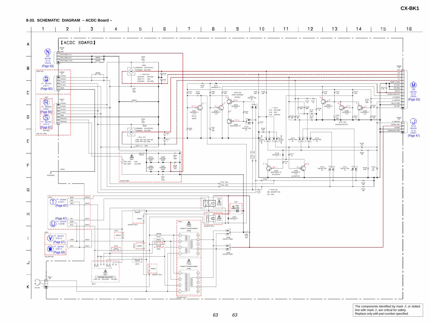
CX-BK1
6363
EP001
R147
R108
R113
R118 R119 R120
R128
Q109Q108
Q107
R121 R123C122
R110 R111
R112
R114
C003
R139
R137
R134
R109
R107R106
D140
D139
D118 R117
C123
R122
Q106Q105
R116
R148
R156
R115
Q103
Q104
R103R105
C121R102
C120R101
D114
D115
CN006
CN011
D023
D006
D005
C029
CN004
CN003
R131
R130
Q101 Q102
R157
D116
D112 D113
D007D008
D010 D009
C001
C010
C002PR001
F001
C012
C011
C015
C016
D002
C004
D004
JW001
JW090
JW082
JW091
CN009
CN012
W013
W014
W015
W016
W017
W018
R001RY502
RY001
PT005
PT006
JW007
JW006
JW008
PR005
JW018
JW019
JW020
JW003
JW004
JW005
S001
R140
R138
R104 D111
C008
C007
R136
D117 C124
R133
R132
R135
39k
56k
2.2k
100 15k 10k
1k
2SC3052F-T1-LF
2SC3052F-T1-LF
2SC3052F-T1-LF
15k 33k4.750V
1k 1k
6.8k
6.8k
0.1 100V
100k
82k
82k
56k
56k56k
1S
S181-T
E8
5L
1S
S184-T
E8
5L
1SS355TE-17 1k
0.2250V
33k
2SC3052F-T1-LF
2SA1235TP-1F
1k
39k
5.6k
12k
2SC3052F-T1-LF
2SA1235TP-1F
10010k
1050V10k
4700p4.7k
1SS184-TE85L
1SS181-TE85L
4P
3P
1SS355TE-17
1SS181-TE85L
1SS184-TE85L
47025V
4P
13P
18k
18k
2SC3052F-T1-LF
2SC3052F-T1-LF
1SS184-TE85L
1SS181-TE85L
1SS184-TE85L
EGP20DL6349
EGP20DL6349
EGP20DL6349
EGP20DL6349
0.1100V
220025V
0.1100V
0.1100V
5P
7P
2.2M1/2W
10k
10k
4.7k 1SS355TE-17
0.1100V
0.1100V
10k
1SS181-TE85L
4725V
10k
∗
∗
∗
∗
*
TUNER/AUX GND
+VH
-VH
+VL
-VL
FAMP-A-GND
REG
VM+9V
POWER MINITOR
O-POWER
C-LIMITER
RELAY GND
C-LIMITER
DC-DET
REG-GND(+7V)
REG-GND(+12V)
REG-GND(+4V)
SP-GND
SP-GND
VSTBY(+9V)
M-GND
VH(AC)
VH(AC)
GND
VL(AC)
VL(AC)
VH(AC)
VH(AC)
GND
VL(AC)
VL(AC)
REG(AC)
REG(AC)
(CHASSIS)
Q107-109
VOLTAGE DETECT
AC DETETCAC DETETC
Q102-104
OVER CURRENT
DETECT
DRIVE
RELAY
R157∗
2.7k (E51,MX)
(US)
(AEP,UK)
3.3k
3.9k
(E51,MX)
(US)T5AL 125V
T5AL 250V
(US,E51,MX)
(E51,MX)
D3SBA20 (US,AEP,UK)
∗
(E51,MX)
(US)
(AEP,UK)
C015,016
3300 63V
3300 71V
3300 80V
(E51,MX)
(US,AEP,UK)
D10XB20
D5SBA20
(US)
(US, E51, MX)
(AEP, UK)
GRN
RED
GRN
YEL
BLU
RED
BRN
ORG
(E51)
(US,AEP,UK)
(MX)
(AC IN)
-1 -2
(E51)
(EXCEPT E51)
POWER TRANSFORMER
(SUB)
POWER TRANSFORMER
(SUB)
(EXCEPT E51)
(E51)
(E51)
(MX)
(E51)
(E51
)
(E51)
(E51)
(EXCEPT E51)
-1 -2
VOLTAGE SELECTOR
220-230V 240V120V
(E51)
(E51,MX) D5SBA20
(EXCEPT E51)
(US)
∗
(US)
R132,135
39k
47k
(EXCEPT US)
∗ C011, 012
4700 35V4700 50V
(US, AEP, UK)(E51, MX)
∗
∗
8-33. SCHEMATIC DIAGRAM – ACDC Board –
(Page 65)
(Page 67)
(Page 67)
(Page 67)
(Page 67)
(Page 65)
(Page 65)
(Page 53)
(Page 53)
(Page 47)
The components identified by mark 0 or dottedline with mark 0 are critical for safety.Replace only with part number specified.
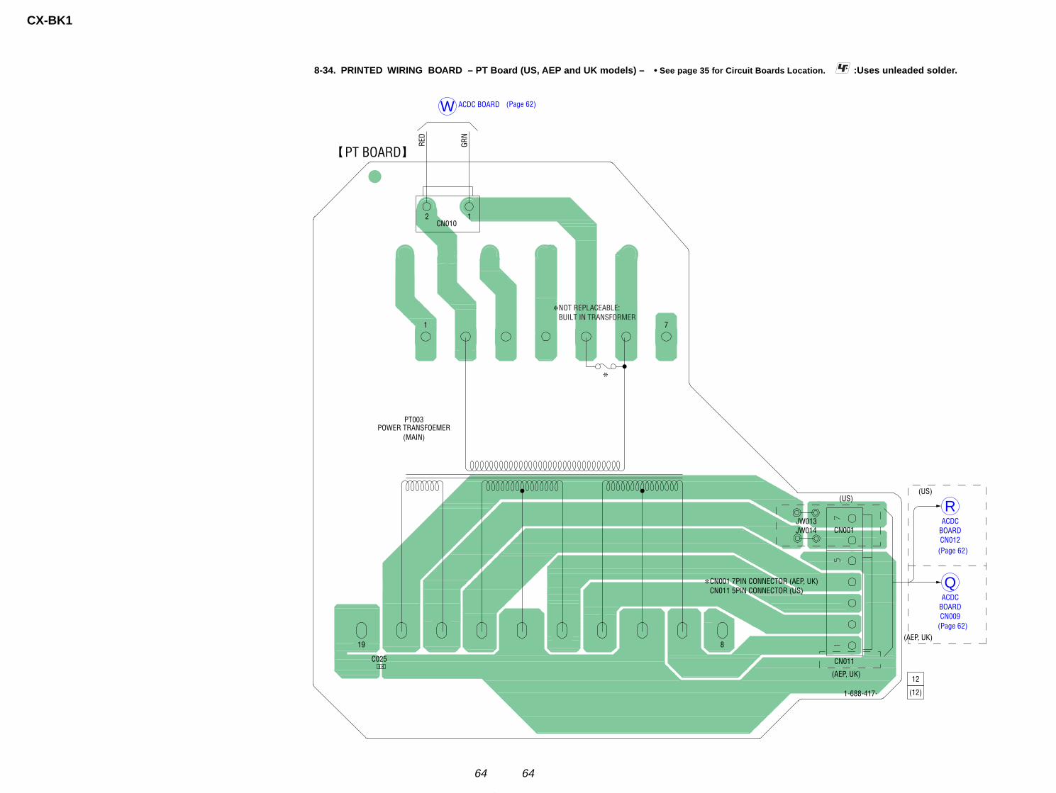
CX-BK1
6464
8-34. PRINTED WIRING BOARD – PT Board (US, AEP and UK models) – • See page 35 for Circuit Boards Location. :Uses unleaded solder.
CN010
PT003
CN011
CN001
C025
JW013JW014
1-688-417-
12
(12)
PT BOARD
12
RED
GRN
ACDC BOARDW
POWER TRANSFOEMER(MAIN)
1 7
19 8
∗
∗NOT REPLACEABLE: BUILT IN TRANSFORMER
(AEP, UK)
(US)(US)
(AEP, UK)
∗CN001 7PIN CONNECTOR (AEP, UK) CN011 5PIN CONNECTOR (US)
ACDCBOARDCN009
Q
ACDCBOARDCN012
R
(Page 62)
(Page 62)
(Page 62)
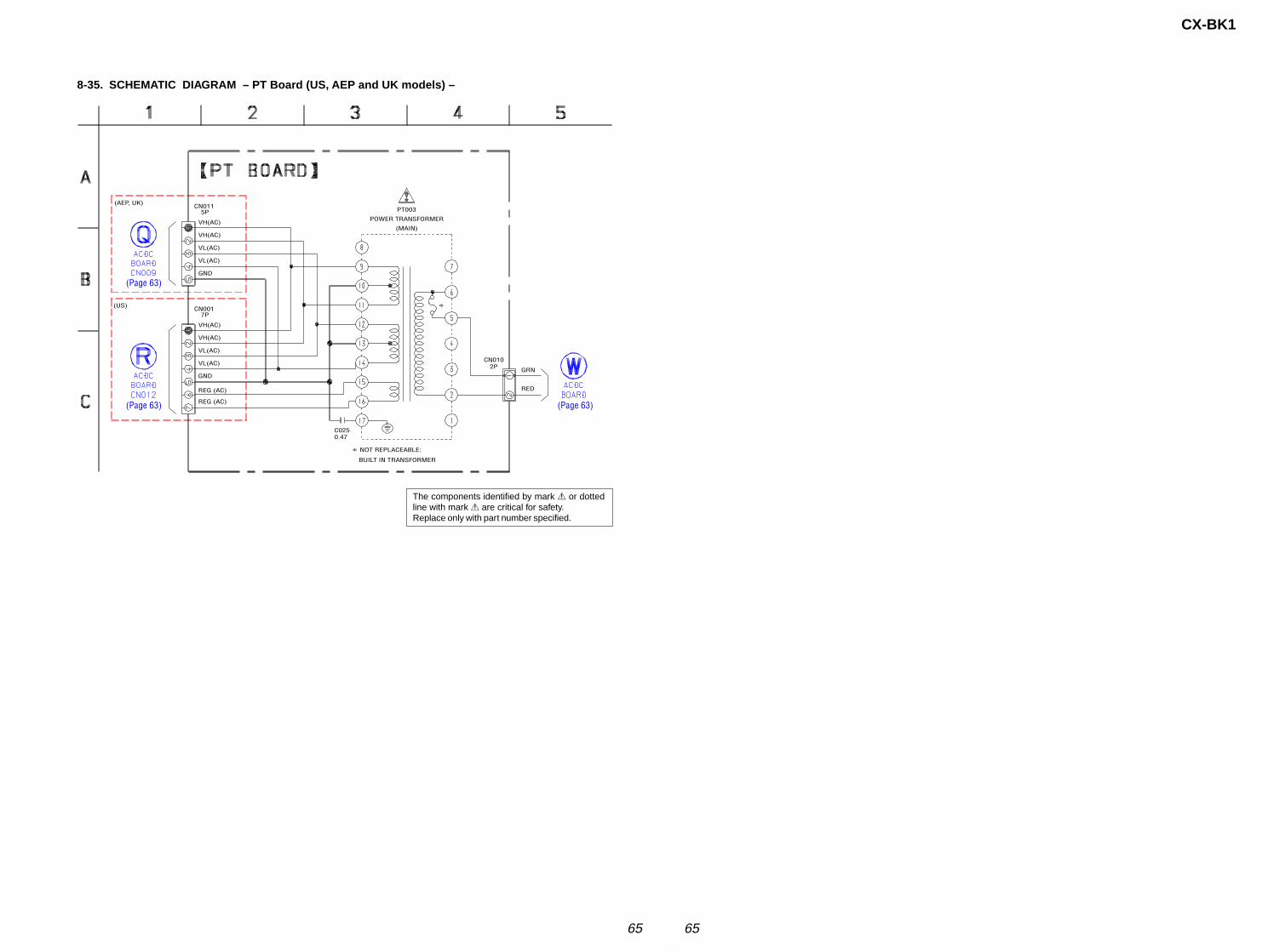
CX-BK1
6565
8-35. SCHEMATIC DIAGRAM – PT Board (US, AEP and UK models) –
PT003
CN010
C025
CN001
CN011
2P
0.47
7P
5P
VH(AC)
VH(AC)
VL(AC)
VL(AC)
GND
VH(AC)
VH(AC)
VL(AC)
VL(AC)
GND
∗
POWER TRANSFORMER
(MAIN)
GRN
RED
BUILT IN TRANSFORMER
NOT REPLACEABLE:∗
(AEP, UK)
(US)
REG (AC)
REG (AC)
The components identified by mark 0 or dottedline with mark 0 are critical for safety.Replace only with part number specified.
(Page 63)
(Page 63)
(Page 63)
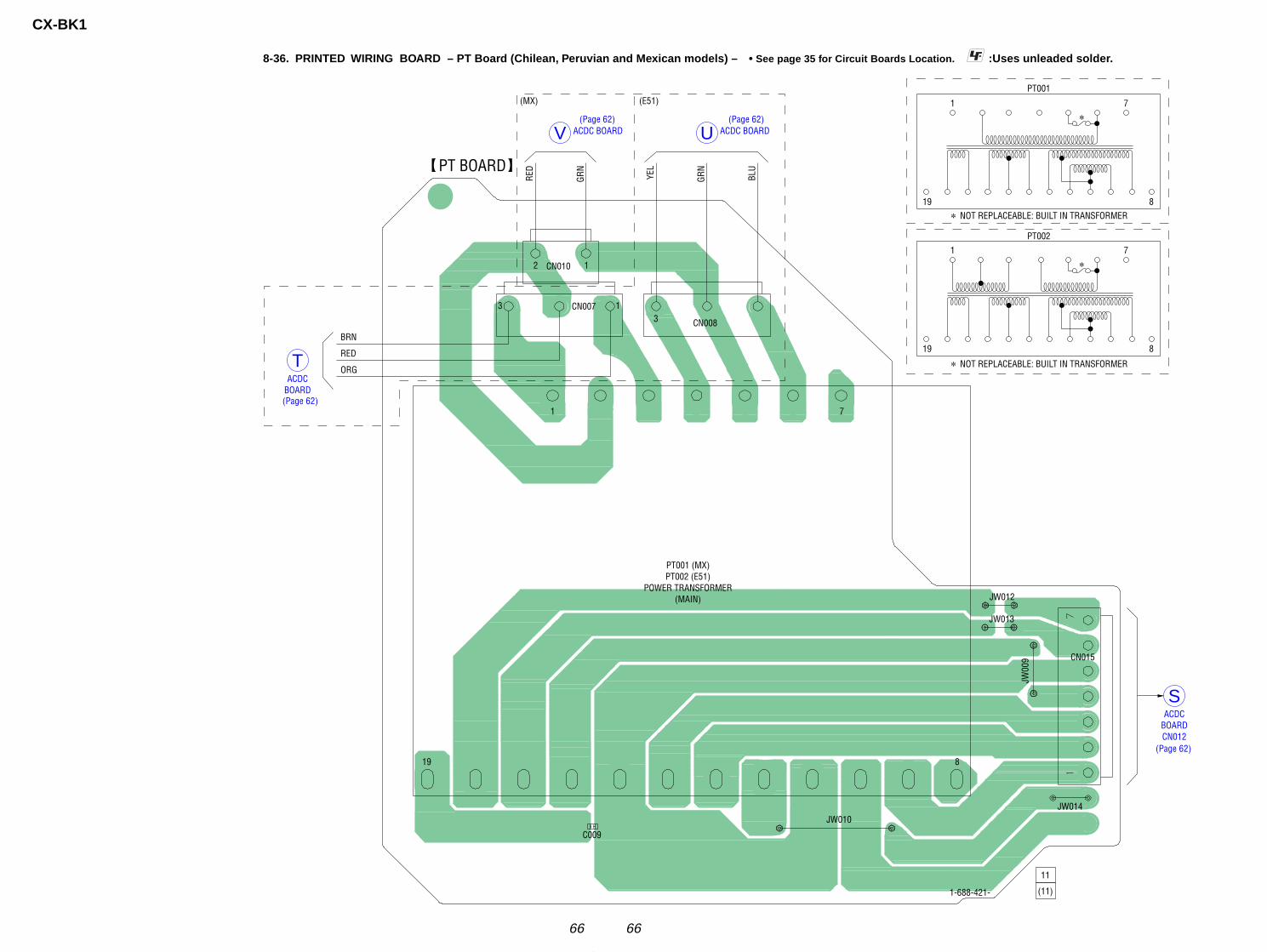
CX-BK1
6666
8-36. PRINTED WIRING BOARD – PT Board (Chilean, Peruvian and Mexican models) – • See page 35 for Circuit Boards Location. :Uses unleaded solder.
JW00
9
JW010
CN010
CN007
CN008
JW014
CN015
C009
JW012
JW013
PT BOARD
1-688-421-
11
(11)
1 7
8
31
12
3
RED
BRN
RED
ORG
GRN
YEL
GRN
BLU
ACDCBOARD
T
ACDC BOARDV ACDC BOARDU
(MX) (E51)
PT001 (MX)PT002 (E51)
POWER TRANSFORMER(MAIN)
ACDCBOARDCN012
S
1
19 8
∗
19
∗1 7
819
∗NOT REPLACEABLE: BUILT IN TRANSFORMER
∗NOT REPLACEABLE: BUILT IN TRANSFORMER
PT001
PT002
7(Page 62)
(Page 62) (Page 62)
(Page 62)
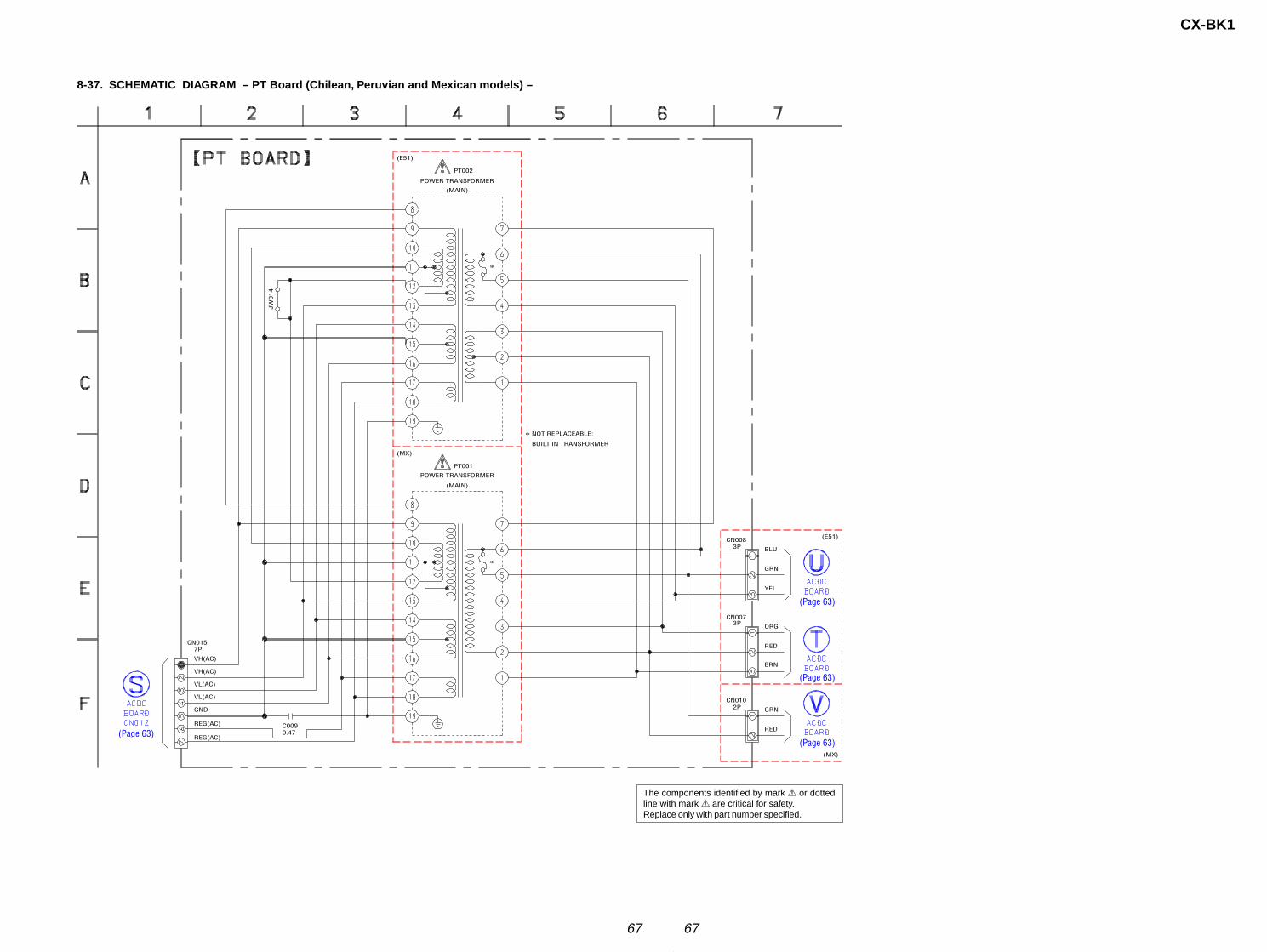
CX-BK1
6767
8-37. SCHEMATIC DIAGRAM – PT Board (Chilean, Peruvian and Mexican models) –
C009
CN015
CN010
CN007
CN008
PT002
PT001
JW014
0.47
7P
2P
3P
3P
∗
VH(AC)
VH(AC)
VL(AC)
VL(AC)
GND
∗
POWER TRANSFORMER
(MAIN)
POWER TRANSFORMER
(MAIN)
(E51)
(MX)
BUILT IN TRANSFORMER
NOT REPLACEABLE:∗
GRN
BLU
YEL
ORG
RED
BRN
GRN
RED
(E51)
(MX)
REG(AC)
REG(AC)
The components identified by mark 0 or dottedline with mark 0 are critical for safety.Replace only with part number specified.
(Page 63)
(Page 63)
(Page 63)
(Page 63)
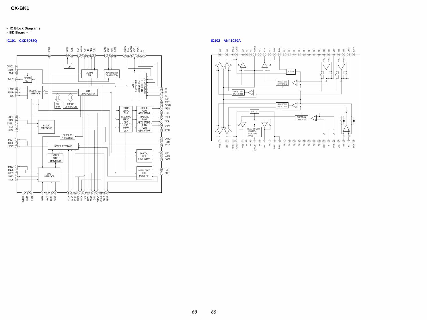
CX-BK1
6868
• IC Block Diagrams– BD Board –
IC101 CXD3068Q IC102 AN41020A
DOUT
LRCKPCMD
BCK
DVDD2ASYEMD2
EMPHXTSL
DVSS2XTAI
XTAO
SQSOSQCKSCSYSBSOEXCK
SOUTSOCKXOLT
SETEVCTES1TEST1DVSS1FRDR
FFDR
TRDR
TFDR
SRDR
SFDR
DVDD1FSTOSSTP
MDPLOCKPWMI
FOKDFCT
DIGITALCLV
PROCESSOR
OSC
DIGITALOUT
EFMDEMODULATOR
32KRAM
ERRORCORRECTOR
D/A DIGITALINTERFACE
MIRR, DFCT,FOK
DETECTORCPU
INTERFACE
SUBCODEPROCESSOR
SERVOAUTO
SEQUENCER
SERVO INTERFACE
DVDD
0
XRST
MUT
E
DATA
XLAT
CLOK
SENS
SCLK
ATSK
WFC
KXU
GFXP
CK GFS
C2PO
SCOR C4M
WDC
KDV
SS0
COUT
MIR
R
AVDD
0IG
ENAV
SS0
ADIO
RFDC
CE TEAVSS
1RF
ACAS
YIAS
YO
BIAS
AVDD
1PC
OFI
LIFI
LOCL
TV
V16M
VCTL
VPCO
59 58 57 56 55 54 53 52 51 50 49 48 47 46 45 44 43 42 41
1 2 3 4 5 6 7 8 9 10 11 12 13 14 15 16 17 18 19 20
2122
232425
262728
29
30
31
32
33
34353637383940
8079787776
757473
7271706968
676665
64
636261
OPER
ATIO
NAL
AMPL
IFIE
R &
ANAL
OG S
WIT
CH
A/D
CONV
ERTE
R
FOCUSPWM
GENERATORTRACKING
PWMGENERATOR
SLEDPWM
GENERATOR
FOCUSSERVO
DSPTRACKING
SERVODSPSLED
SERVODSP
ASYMMETRYCORRECTOR
DIGITALPLL
CLOCKGENERATOR
60
1 2 3 4 5 6 7 98 21 22 23 24 25 26 27 28
29303132333435363738394041424344454647484950515253545556
16 17 18 19 20151413121110
PGND
1
PGND
1
DIRECTIONDETECTION
DIRECTIONDETECTION
RESET CIRCUIT .STANDBY .BAND-GAP .SVCC
DIRECTIONDETECTION
DIRECTIONDETECTION
PVCC/2
PVCC/2
PVCC
/2
PVCC
1
PVCC
1
VO2+
VO1+
VO1-
IN1+
IN1-
OPO1
OPO2
SGND
IN2+
IN2-
NC NC NC NC NC NC NC NC NC NC NC NCVO2-
PGND
2
PGND
2
STAN
DBY
PVCC
2
PVCC
2
VO3-
VO4-
VO4+
VREF IN4
IN4R
IN3+
SVCC
OPO3 IN3-NC NC NC NC NC NC NC NC NC NC NC NC
VO3+

69
CX-BK1
IC103 CXA2647N-T4
ROM/RW
ROM/RW
RF OFF AT VCC
VOFST
VOFSTDVC
VC
VC
VC
ROM/RW
VC
VC
3029
28+–+
–
VCVCC
DVC
27
262524
ROM/RW
EQ
23
22
21
20
19
RFACVCA
VCC
+–
DVC
+–
+–
ROM/RW
VC
ROM/RW
DVC
+–
3
A
B
C
D
BC
A
A
A
BCD
B C D D
+–
1
2 APC AMP
5
6789
4RFAC
SUMMINGAMP
ROM/RW
DVC OR Hi-ZSLEEP, APC OFF
VOFST
VC
ROM/RW
+–
10
18
17
16
B
D
A
C
13
14
15
12
EQ IN
LD
PD
GND
ABCD
AC SUM
E
DVCC
DVC
RFAC
SW
DC OFSTRFDCI
RFDC
VC
RFCVFCBST
RFG
VCC
CEI
CE
TE BAL
TE
FEI
FE
VC
+–
VC
+–
11 GMF
GM
ROM/RW(L/H)
VOFST
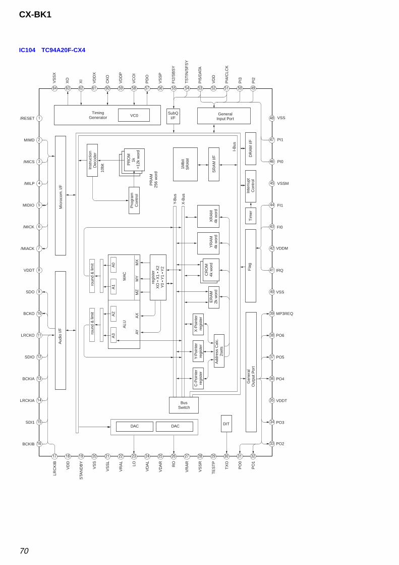
70
CX-BK1
IC104 TC94A20F-CX4
33
34
35
36
37
38
39
40
41
42
1
8
43
61626364 60 59 56 52 50
47
46
45
44
48
49
25 26 27 28 29 30 31 3217 18 19 20 21 22 23 24
9
10
11
2
3
4
5
6
7
58 57 55 53 51
12
13
14
15
16
54
PO2
PO3
VDDT
PO
1
PO
0
TX
O
TE
ST
P
VS
SR
DITDACDAC
BusSwitch
PO4
PO5
PO6
MP3REQ
Gen
eral
Out
put P
ort
Add
ress
Cal
c.2s
ets
Y-P
oint
erre
gist
erC
-Poi
nter
regi
ster
X-P
oint
erre
gist
er
VSS
IRQ
VDDM
FI0
FI1
Fla
g
ER
AM
2k w
ord
CR
OM
4k w
ord
YR
AM
4k w
ord
XR
AM
4k w
ord
Tim
erIn
terr
upt
Con
trol
DR
AM
I/F
I-B
us
SR
AM
I/F
1Mbi
tS
RA
MX
-Bus
Y-B
us
PI0
PI1
VSS
VSSM
GeneralInput Port
SubQI/F
VC0Timing
Generator
PR
AM
256
wor
d
PR
OM
1k
=12
k w
ord
10bi
t
Inst
ruct
ion
Dec
oder
Pro
gram
Con
trol
Mic
roco
m. I
/F
regi
ster
XO
• X
1 •
X2
Y0
• Y1
• Y2
MX
MY
MZ
MA
C
A0
A1
AX
AY
ALU
A2
A3
roun
d &
lim
itro
und
& li
mit
Aud
io I/
F
BCKIB
SDI1
LRCKIA
BCKIA
SDIO
LRCKO
BCKO
SDO
VDDT
/MIACK
/MICK
MIDIO
/MILP
/MICS
MIMD
/RESET
PI2
PI3
PI4
/CLC
K
VD
D
PI5
/DAT
A
TS
TIN
/SF
SY
FI2
/SB
SY
VS
SP
PD
O
VC
OI
VD
DX
VS
SX
CK
O
VD
DP
XI
XO
VR
AR
RO
VD
AR
VD
AL
LO
VR
AL
VS
SL
VS
S
STA
ND
BY
VD
D
LRC
KIB
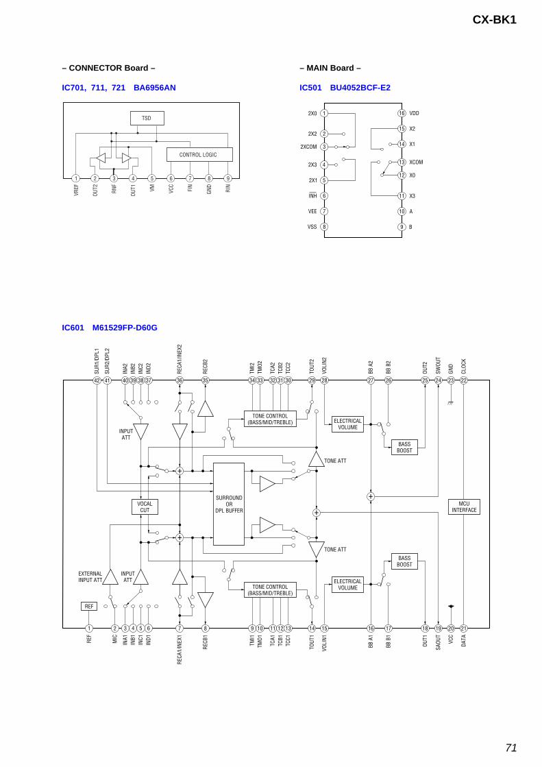
71
CX-BK1
– CONNECTOR Board –
IC701, 711, 721 BA6956AN
1 2 3 4 5 6 7 8 9
CONTROL LOGIC
TSD
VREF
OUT2
OUT1
RNF
VM VCC
FIN
GND
RIN
– MAIN Board –
IC501 BU4052BCF-E2
1
2
3
4
5
6
7
8
16
15
14
13
12
11
10
9
2X0
X2
VDD
X1
XCOM
X0
X3
A
BVSS
VEE
INH
2X1
2X3
2XCOM
2X2
IC601 M61529FP-D60G
1
REF
2
MIC
3
INA1
REF
EXTERNALINPUT ATT
INPUTATT
4
INB1
5
INC1
6
IND1
7
RECA
1/IN
EX1
8
RECB
1
9
TMI1
10
TMO1
11
TCA1
12
TCB1
13
TCC1
14
TOUT
1
16
BB A
1
17
BB B
1
15
VOLI
N1
VOCALCUT
TONE ATT
+
TONE CONTROL(BASS/MID/TREBLE)
ELECTRICALVOLUME
18
OUT1
19
SAOU
T
20
VCC
BASSBOOST
21
DATA
MCUINTERFACE
42
SUR1
/DPL
1
41
SUR2
/DPL
2
40
INA2
INPUTATT
39
INB2
38
INC2
37
IND2
36
RECA
1/IN
EX2
35
RECB
2
34
TMI2
33
TMO2
32
TCA2
31
TCB2
30
TCC2
29
TOUT
2
27
BB A
2
26BB
B2
28
VOLI
N2
+TONE ATT
TONE CONTROL(BASS/MID/TREBLE) ELECTRICAL
VOLUME
25
OUT2
24
SWOU
T
23
GNDBASS
BOOST
22
CLOC
K
+SURROUNDOR
DPL BUFFER
+
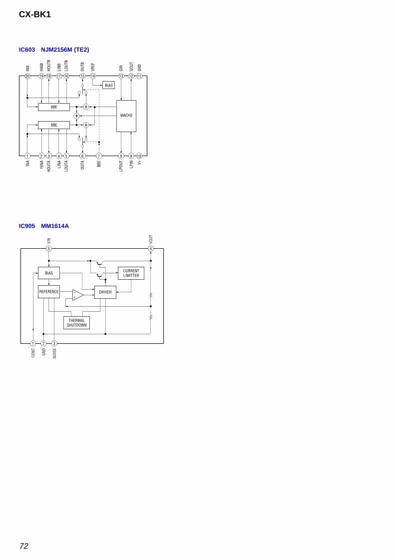
72
CX-BK1
IC603 NJM2156M (TE2)
BBE
BIAS
MACH3
19 18
HOUT
B
HINB
20
INB
17 16
LOUT
B
LINB
13
GIN
12
GOUT
11
GND
++
15OU
TB
BBE
2 3
HOUT
A
HINA
1
INA
4 5
LOUT
A
LINA
8
LPOU
T
9
LPIN
10
V+
+
6
OUTA
7
BBE
14
VREF
IC905 MM1614A
2
5
VIN
4
VOUT
GND
1
CONT
3
NOIS
E
DRIVER
THERMALSHUTDOWN
BIAS
REFERENCE+–
CURRENTLIMITTER

73
CX-BK1
8-38. IC PIN FUNCTION DESCRIPTION
• BD BOARD IC101 CXD3068Q (DIGITAL SERVO, DIGITAL SERVO PROCESSOR)
Pin No. Pin Name I/O Description
1 DVDD0 — Power supply terminal (+3.3V) (digital system)
2 XRST I Reset signal input from the system controller “L”: reset
3 MUTE I Muting on/off control signal input terminal “H”: muting on Not used
4 DATA I Serial data input from the system controller
5 XLAT I Serial data latch pulse signal input from the system controller
6 CLOK I Serial data transfer clock signal input from the system controller
7 SENS O Internal status (SENSE) signal output to the system controller
8 SCLK I SENSE serial data reading clock signal input from the system controller
9 ATSK I/O Input/output terminal for anti-shock Not used
10 WFCK O Write frame clock signal output terminal Not used
11 RFCK O RFCK signal output terminal Not used
12 XPCK O XPCK signal output terminal Not used
13 GFS O Guard frame sync signal output terminal Not used
14 C2PO O C2 pointer signal output terminal Not used
15 SCOR O Subcode sync (S0+S1) detection signal output to the system controller
16 C4M O 4.2336 MHz clock signal output terminal Not used
17 WDCK O Guard subcode sync (S0+S1) detection signal output terminal Not used
18 DVSS0 — Ground terminal (digital system)
19 COUT O Numbers of track counted signal output terminal Not used
20 MIRR O Mirror signal output terminal Not used
21 DFCT I/O Defect signal input/output terminal Not used
22 FOK O Focus OK signal output terminal Not used
23 PWMI I Spindle motor external control signal input terminal Not used
24 LOCK O GFS is sampled by 460 Hz “H” output when GFS is “H” Not used
25 MDP O Spindle motor servo drive signal output to the motor/coil drive IC
26 SSTP I Detection signal input from limit in switch The optical pick-up is inner position when “H”
27 FSTO O 2/3 divider output terminal Not used
28 DVDD1 — Power supply terminal (+3.3V) (digital system)
29 SFDR O Sled servo drive PWM signal (+) output terminal
30 SRDR O Sled servo drive PWM signal (–) output terminal
31 TFDR O Tracking servo drive PWM signal (+) output terminal
32 TRDR O Tracking servo drive PWM signal (–) output terminal
33 FFDR O Focus servo drive PWM signal (+) output terminal
34 FRDR O Focus servo drive PWM signal (–) output terminal
35 DVSS1 — Ground terminal (digital system)
36 TEST I Input terminal for the test
37 TES1 I Input terminal for the test
38 VC I Middle point voltage (+1.65V) input terminal
39 FE I Focus error signal input from the RF amplifier
40 SE I Sled error signal input from the RF amplifier
41 TE I Tracking error signal input from the RF amplifier
42 CE I Middle point servo analog signal input
43 RFDC I RF signal input from the RF amplifier
44 ADIO O Output terminal for the test Not used
45 AVSS0 — Ground terminal (analog system)
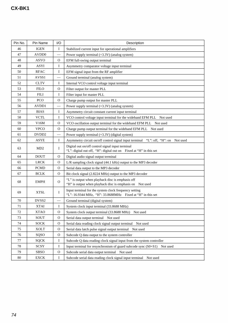
74
CX-BK1
Pin No. Pin Name I/O Description
46 IGEN I Stabilized current input for operational amplifiers
47 AVDD0 — Power supply terminal (+3.3V) (analog system)
48 ASYO O EFM full-swing output terminal
49 ASYI I Asymmetry comparator voltage input terminal
50 RFAC I EFM signal input from the RF amplifier
51 AVSS1 — Ground terminal (analog system)
52 CLTV I Internal VCO control voltage input terminal
53 FILO O Filter output for master PLL
54 FILI I Filter input for master PLL
55 PCO O Charge pump output for master PLL
56 AVDD1 — Power supply terminal (+3.3V) (analog system)
57 BIAS I Asymmetry circuit constant current input terminal
58 VCTL I VCO control voltage input terminal for the wideband EFM PLL Not used
59 V16M O VCO oscillation output terminal for the wideband EFM PLL Not used
60 VPCO O Charge pump output terminal for the wideband EFM PLL Not used
61 DVDD2 — Power supply terminal (+3.3V) (digital system)
62 ASYE I Asymmetry circuit on/off control signal input terminal “L”: off, “H”: on Not used
63 MD2 IDigital out on/off control signal input terminal“L”: digital out off, “H”: digital out on Fixed at “H” in this set
64 DOUT O Digital audio signal output terminal
65 LRCK O L/R sampling clock signal (44.1 kHz) output to the MP3 decoder
66 PCMD O Serial data output to the MP3 decoder
67 BCLK O Bit clock signal (2.8224 MHz) output to the MP3 decoder
68 EMPH O“L” is output when playback disc is emphasis off“H” is output when playback disc is emphasis on Not used
69 XTSL IInput terminal for the system clock frequency setting“L”: 16.9344 MHz, “H”: 33.8688MHz Fixed at “H” in this set
70 DVSS2 — Ground terminal (digital system)
71 XTAI I System clock input terminal (33.8688 MHz)
72 XTAO O System clock output terminal (33.8688 MHz) Not used
73 SOUT O Serial data output terminal Not used
74 SOCK O Serial data reading clock signal output terminal Not used
75 XOLT O Serial data latch pulse signal output terminal Not used
76 SQSO O Subcode Q data output to the system controller
77 SQCK I Subcode Q data reading clock signal input from the system controller
78 SCSY I Input terminal for resynchronism of guard subcode sync (S0+S1) Not used
79 SBSO O Subcode serial data output terminal Not used
80 EXCK I Subcode serial data reading clock signal input terminal Not used
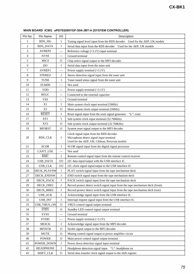
75
CX-BK1
• MAIN BOARD IC901 uPD703260YGF-S04-JBT-A (SYSTEM CONTROLLER)
Pin No. Pin Name I/O Description
1 RDS_SIG I Tuning signal level input from the RDS decoder Used for the AEP, UK models
2 RDS_DATA I Serial data input from the RDS decoder Used for the AEP, UK models
3 AVREF0 — Reference voltage (+3.1V) input terminal
4 AVSS — Ground terminal
5 MICS O Chip select signal output to the MP3 decoder
6 DO I Serial data input from the tuner unit
7 AVREF1 — Power supply terminal (+3.1V)
8 STEREO I Stereo detection signal input from the tuner unit
9 TUNE I Tuner tuned status signal from the tuner unit
10 FLMD0 — Not used
11 VDD — Power supply terminal (+3.1V)
12 REGC — Connected to the external capacitor
13 VSS — Ground terminal
14 X1 I Main system clock input terminal (5MHz)
15 X2 O Main system clock output terminal (5MHz)
16 RESET I Reset signal input from the reset signal generator “L”: reset
17 XT1 I Sub system clock input terminal (32.768kHz)
18 XT2 O Sub system clock output terminal (32.768kHz)
19 MP3RST O System reset signal output to the MP3 decoder
20 RDS_CLK IClock signal input from the RDS decoderMicrophone detect signal input terminalUsed for the AEP, UK, Chilean, Peruvian models
21 SCOR I SCOR signal input from the digital signal processor
22 CAN'T_USE — Not used
23 RMC I Remote control signal input from the remote control receiver
24 USB_DATA I/O I2C data input/output with the USB interface IC
25 USB_CLK I/O I2C clock signal input/output to the USB interface IC
26 DECK_PLAYSW I PLAY switch signal input from the tape mechanism deck
27 DECK_ENDSW I END switch signal input from the tape mechanism deck
28 DECK_PACK I PACK switch signal input from the tape mechanism deck
29 DECK_FREC I Record protect detect switch signal input from the tape mechanism deck (front)
30 DECK_RREC I Record protect detect switch signal input from the tape mechanism deck (rear)
31 USB_ACK I Acknowledge signal input from the USB interface IC
32 USB_INT I Interrupt request signal input from the USB interface IC
33 USB_VBUS_ON O VBUS control signal output terminal
34 STBY O Standby LED control signal output terminal
35 EVSS — Ground terminal
36 EVDD — Power supply terminal (+3.1V)
37 MIACK I Acknowledge signal input from the MP3 decoder
38 MP3STB O Strobe signal output to the MP3 decoder
39 MUTE O Muting control signal output to power amplifier circuit
40 POWER O Main power control signal output terminal
41 POWER_DOWN I Power down detection signal input terminal
42 HEADPHONE I Headphone detection signal input “L”: headphone on
43 SHIFT_CLK O Serial data transfer clock signal output to the shift register

76
CX-BK1
Pin No. Pin Name I/O Description
44 SHIFT_DATA O Serial data output to the shift register
45 SHIFT_STB O Strobe signal output to the shift register
46 PLLCE O Latch signal output to the tuner unit
47 PWM1 O PWM signal output for focus offset adjustment
48 MCLK O Serial data transfer clock signal output to the tuner unit and input select IC
49 PWM3 O PWM signal output for RF offset adjustment
50 MDATA O Serial data output to the tuner unit and input select IC
51 PWM2 O PWM signal output for tracking offset adjustment
52 DATA O Serial data output to the digital signal processor
53 LCD_DATA O Serial data output to the LCD driver
54 LCD_CLK O Serial data transfer clock output to the LCD driver
55 CLOCK O Serial data transfer clock output to the digital signal processor
56 SQSO I Sub-Q data input from the digital signal processor
57 SQCK O Sub-Q clock output to the digital signal processor
58 SENS I SENS signal input from the digital signal processor
59 LDON O Laser diode on/off control signal output to the automatic power control circuit “H”: laser on
60 XLT O Control data latch signal output to the digital signal processor
61 XRST O System reset signal output to the digital signal processor and motor/coil drive IC
62 MICK O Serial data transfer clock signal output to the MP3 decoder
63 LCD_CE O Latch signal output to the LCD driver
64 MIDIO I/O Serial data input/output to/form the MP3 decoder
65 MP3REQ O Request signal output to the MP3 decoder
66 MILP O Latch pulse signal output to the MP3 decoder
67 ELV_E2 I ELV_E2 switch signal input from the CD mechanism
68 ELV_E3 I ELV_E3 switch signal input from the CD mechanism
69 ELV_E1 I ELV_E1 switch signal input from the CD mechanism
70 SLD_E3 I SLD_E3 switch signal input from the CD mechanism
71 BVSS — Ground terminal
72 BVDD — Power supply terminal
73 SLD_E1 I SLD_E1 switch signal input from the CD mechanism
74 SW5-B I SW4 switch signal input from the CD mechanism
75 ELV_POS O Elevator motor control signal output for the CD mechanism
76 SLD_POS O Loading motor control signal output for the CD mechanism
77 LOD_POS O Sled motor control signal output for the CD mechanism
78 SW4 I SW5-B switch signal input from the CD mechanism
79 SW2-A I SW2-A switch signal input from the CD mechanism
80 SW3 I SW3 switch signal input from the CD mechanism
81 D_SENSOR I Disc sensor signal input from the CD mechanism
82 SW1-A I SW1-A switch signal input from the CD mechanism
83 SW2-B I SW2-B switch signal input from the CD mechanism
84 SW5-A I SW5-A switch signal input from the CD mechanism
85 LOD_NEG O Sled motor control signal output for the CD mechanism
86 SLD_NEG O Loading motor control signal output for the CD mechanism
87 ELV_NEG O Elevator motor control signal output for the CD mechanism
88 SLD_E0 I SLD_E0 switch signal input from the CD mechanism
89 SLD_E2 I SLD_E2 switch signal input from the CD mechanism

77
CX-BK1
Pin No. Pin Name I/O Description
90 ELV_E0 I ELV_E0 switch signal input from the CD mechanism
91 RE_TRE I Jog dial pulse input from the rotary encoder (TREBLE/MIDDLE)
92 RE_BAS I Jog dial pulse input from the rotary encoder (BASS)
93 RE_VOL I Jog dial pulse input from the rotary encoder (VOLUME)
94 RE_JOG I Jog dial pulse input from the rotary encoder (MULTIJOG)
95 KEY3 I Key input terminal (A/D input)
96 KEY2 I Key input terminal (A/D input)
97 KEY1 I Key input terminal (A/D input)
98 POWER_MONI I Voltage detection signal input terminal
99 LEVEL I Level mater signal input terminal
100 SUFIX I Destination setting input terminal
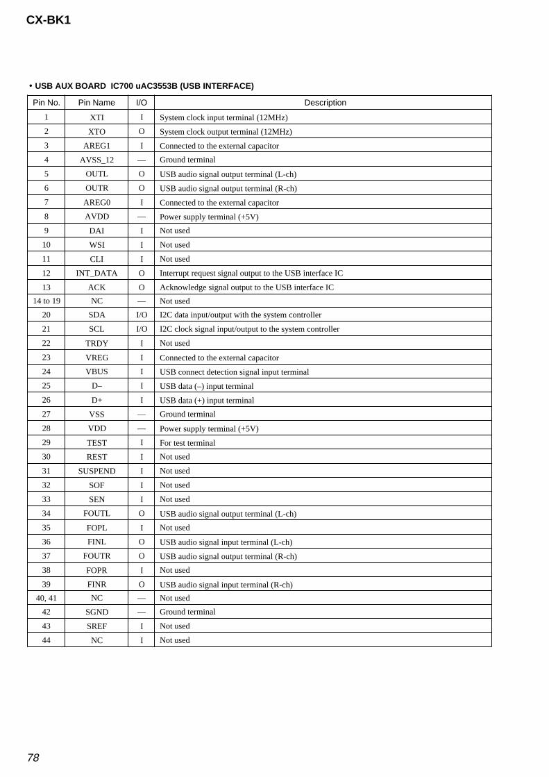
78
CX-BK1
• USB AUX BOARD IC700 uAC3553B (USB INTERFACE)
Pin No. Pin Name I/O Description
1 XTI I System clock input terminal (12MHz)
2 XTO O System clock output terminal (12MHz)
3 AREG1 I Connected to the external capacitor
4 AVSS_12 — Ground terminal
5 OUTL O USB audio signal output terminal (L-ch)
6 OUTR O USB audio signal output terminal (R-ch)
7 AREG0 I Connected to the external capacitor
8 AVDD — Power supply terminal (+5V)
9 DAI I Not used
10 WSI I Not used
11 CLI I Not used
12 INT_DATA O Interrupt request signal output to the USB interface IC
13 ACK O Acknowledge signal output to the USB interface IC
14 to 19 NC — Not used
20 SDA I/O I2C data input/output with the system controller
21 SCL I/O I2C clock signal input/output to the system controller
22 TRDY I Not used
23 VREG I Connected to the external capacitor
24 VBUS I USB connect detection signal input terminal
25 D– I USB data (–) input terminal
26 D+ I USB data (+) input terminal
27 VSS — Ground terminal
28 VDD — Power supply terminal (+5V)
29 TEST I For test terminal
30 REST I Not used
31 SUSPEND I Not used
32 SOF I Not used
33 SEN I Not used
34 FOUTL O USB audio signal output terminal (L-ch)
35 FOPL I Not used
36 FINL O USB audio signal input terminal (L-ch)
37 FOUTR O USB audio signal output terminal (R-ch)
38 FOPR I Not used
39 FINR O USB audio signal input terminal (R-ch)
40, 41 NC — Not used
42 SGND — Ground terminal
43 SREF I Not used
44 NC I Not used
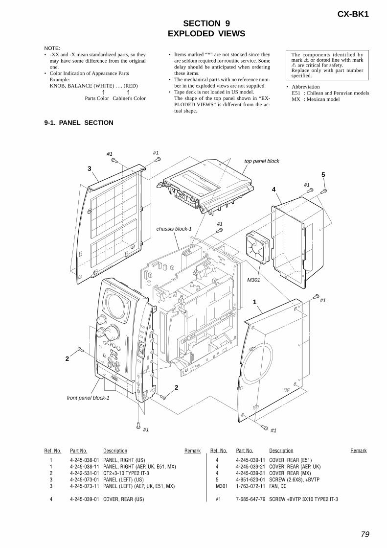
79
CX-BK1SECTION 9
EXPLODED VIEWS
• Items marked “*” are not stocked since theyare seldom required for routine service. Somedelay should be anticipated when orderingthese items.
• The mechanical parts with no reference num-ber in the exploded views are not supplied.
• Tape deck is not loaded in US model.The shape of the top panel shown in “EX-PLODED VIEWS” is different from the ac-tual shape.
NOTE:• -XX and -X mean standardized parts, so they
may have some difference from the originalone.
• Color Indication of Appearance PartsExample:KNOB, BALANCE (WHITE) . . . (RED)
↑ ↑Parts Color Cabinet's Color
9-1. PANEL SECTION
• AbbreviationE51 : Chilean and Peruvian modelsMX : Mexican model
The components identified bymark 0 or dotted line with mark0 are critical for safety.Replace only with part numberspecified.
Ref. No. Part No. Description Remark Ref. No. Part No. Description Remark
1 4-245-038-01 PANEL, RIGHT (US)1 4-245-038-11 PANEL, RIGHT (AEP, UK, E51, MX)2 4-242-531-01 QT2+3-10 TYPE2 IT-33 4-245-073-01 PANEL (LEFT) (US)3 4-245-073-11 PANEL (LEFT) (AEP, UK, E51, MX)
4 4-245-039-01 COVER, REAR (US)
4 4-245-039-11 COVER, REAR (E51)4 4-245-039-21 COVER, REAR (AEP, UK)4 4-245-039-31 COVER, REAR (MX)5 4-951-620-01 SCREW (2.6X8), +BVTPM301 1-763-072-11 FAN, DC
#1 7-685-647-79 SCREW +BVTP 3X10 TYPE2 IT-3
2
2
1
3
4
5
top panel block
chassis block-1
#1#1
#1
#1 #1
#1
#1
M301
front panel block-1
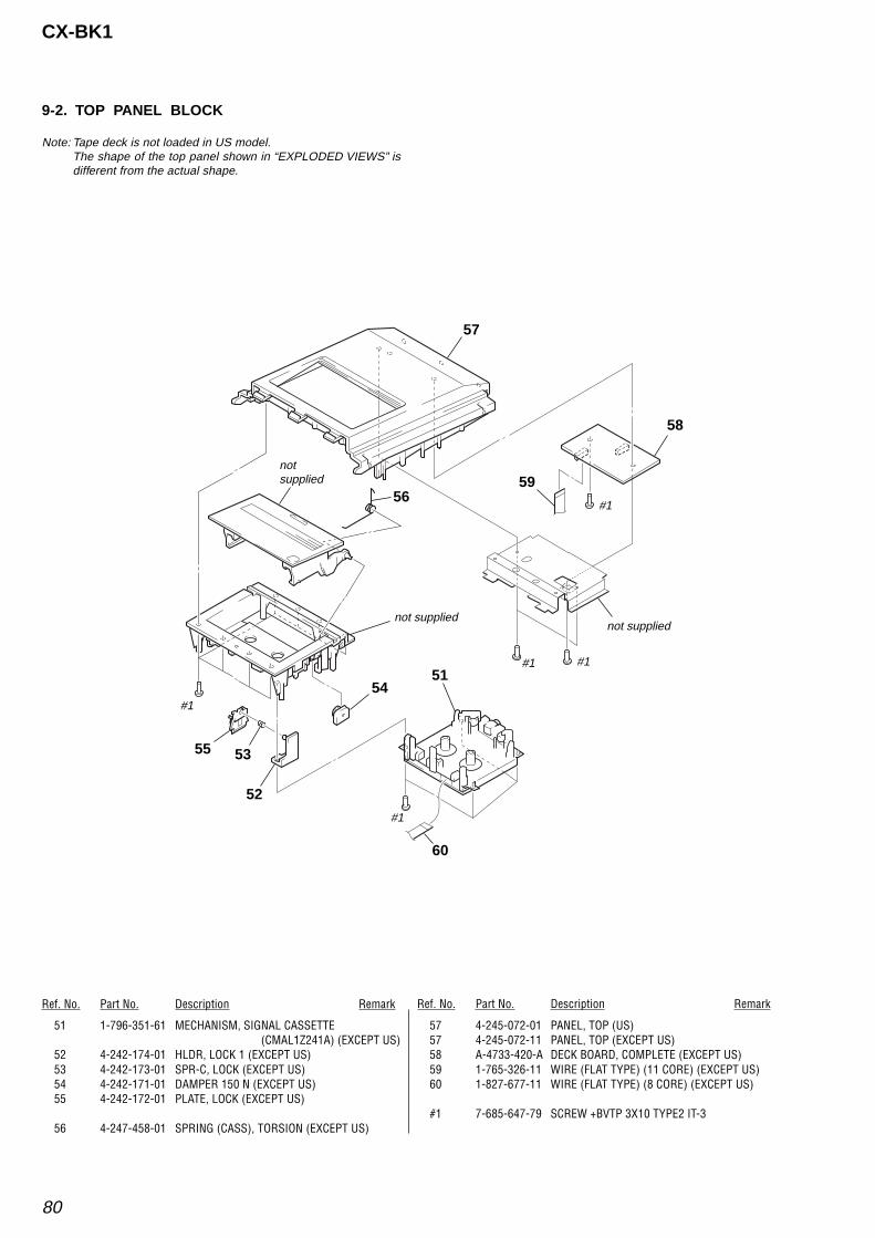
80
CX-BK1
9-2. TOP PANEL BLOCK
Note: Tape deck is not loaded in US model.The shape of the top panel shown in “EXPLODED VIEWS” isdifferent from the actual shape.
Ref. No. Part No. Description Remark Ref. No. Part No. Description Remark
51 1-796-351-61 MECHANISM, SIGNAL CASSETTE(CMAL1Z241A) (EXCEPT US)
52 4-242-174-01 HLDR, LOCK 1 (EXCEPT US)53 4-242-173-01 SPR-C, LOCK (EXCEPT US)54 4-242-171-01 DAMPER 150 N (EXCEPT US)55 4-242-172-01 PLATE, LOCK (EXCEPT US)
56 4-247-458-01 SPRING (CASS), TORSION (EXCEPT US)
57 4-245-072-01 PANEL, TOP (US)57 4-245-072-11 PANEL, TOP (EXCEPT US)58 A-4733-420-A DECK BOARD, COMPLETE (EXCEPT US)59 1-765-326-11 WIRE (FLAT TYPE) (11 CORE) (EXCEPT US)60 1-827-677-11 WIRE (FLAT TYPE) (8 CORE) (EXCEPT US)
#1 7-685-647-79 SCREW +BVTP 3X10 TYPE2 IT-3
5154
52
5355
56
57
59
58
#1
#1
#1#1
#1
notsupplied
not suppliednot supplied
60

81
CX-BK1
9-3. FRONT PANEL BLOCK-1
Ref. No. Part No. Description Remark Ref. No. Part No. Description Remark
101 A-4733-419-A MIC BOARD, COMPLETE (E51, MX)102 1-769-869-11 WIRE (FLAT TYPE) (5 CORE) (E51, MX)103 1-688-414-11 HEADPHONE BOARD104 1-688-407-11 LEFT BUTTON BOARD
105 A-4733-395-A KEY LED RMC BOARD, COMPLETE106 A-4733-399-A USB AUX BOARD, COMPLETE107 3-229-336-01 SCREW, +BVWH TAPPING#1 7-685-647-79 SCREW +BVTP 3X10 TYPE2 IT-3
105
101
102
103
106
104
#1
#1
#1
#1
#1
not supplied(LED board)
not supplied
front panel block-2
107
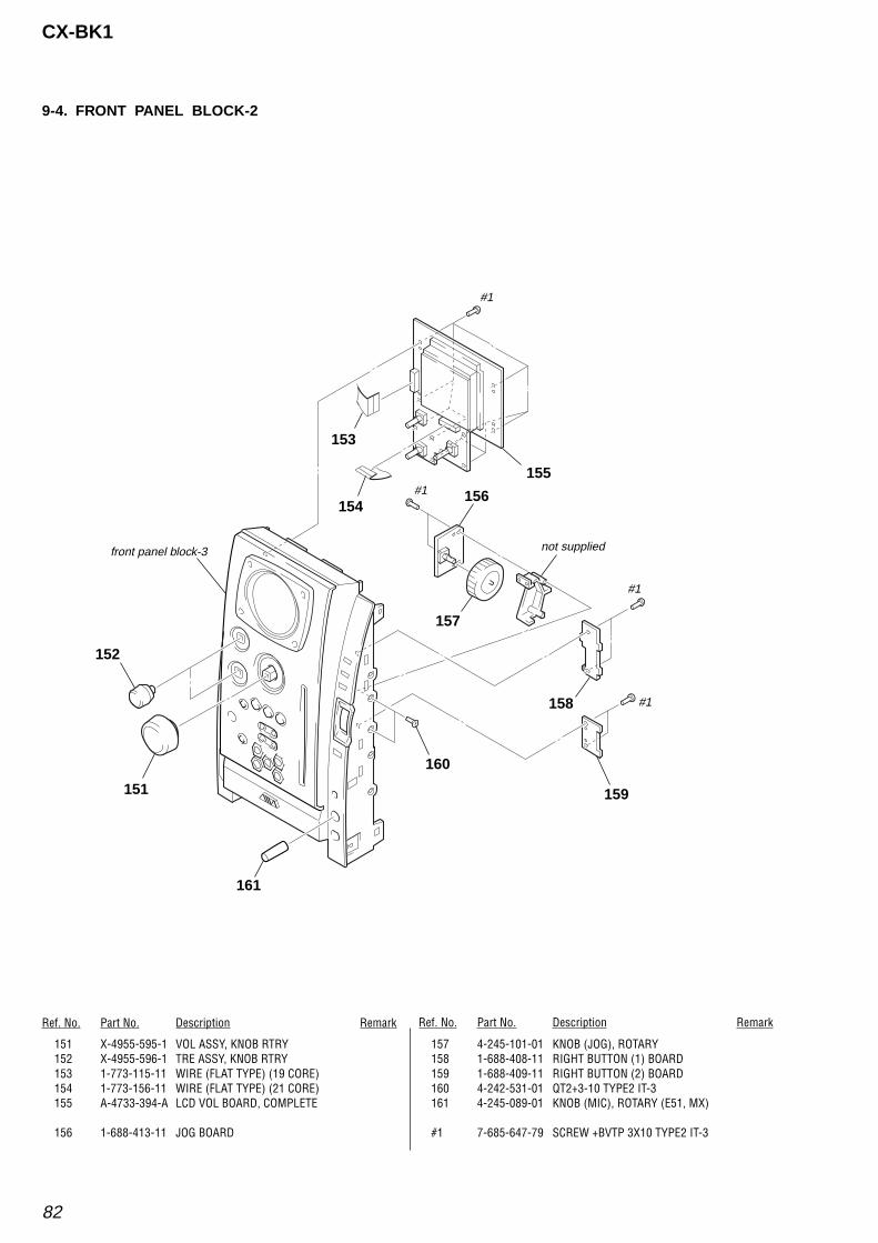
82
CX-BK1
9-4. FRONT PANEL BLOCK-2
Ref. No. Part No. Description Remark Ref. No. Part No. Description Remark
151 X-4955-595-1 VOL ASSY, KNOB RTRY152 X-4955-596-1 TRE ASSY, KNOB RTRY153 1-773-115-11 WIRE (FLAT TYPE) (19 CORE)154 1-773-156-11 WIRE (FLAT TYPE) (21 CORE)155 A-4733-394-A LCD VOL BOARD, COMPLETE
156 1-688-413-11 JOG BOARD
157 4-245-101-01 KNOB (JOG), ROTARY158 1-688-408-11 RIGHT BUTTON (1) BOARD159 1-688-409-11 RIGHT BUTTON (2) BOARD160 4-242-531-01 QT2+3-10 TYPE2 IT-3161 4-245-089-01 KNOB (MIC), ROTARY (E51, MX)
#1 7-685-647-79 SCREW +BVTP 3X10 TYPE2 IT-3
153
154
155
156
157
158
160
161
151
152
159
front panel block-3
#1
#1
#1
not supplied
#1

83
CX-BK1
9-5. FRONT PANEL BLOCK-3
Ref. No. Part No. Description Remark Ref. No. Part No. Description Remark
201 X-4955-409-2 CABI, FR ASSY (US)201 X-4955-727-2 CABINET (FRONT) ASSY (E51, MX)201 X-4955-728-2 CABINET (FRONT) ASSY (AEP, UK)202 4-245-075-01 PANEL, FRONT (US)202 4-245-075-11 PANEL, FRONT (AEP, UK, E51, MX)
203 X-4955-408-1 PANEL,DISP ASSY204 4-245-098-01 REFLECTOR (VOL)205 4-245-078-01 WINDOW, DISPLAY206 4-242-531-01 QT2+3-10 TYPE2 IT-3
207 4-245-088-01 WINDOW, SENSOR208 4-245-094-01 PANEL, CD DIRECT209 4-245-158-01 EMBLEM210 4-245-077-01 PANEL (JOB)211 4-242-091-01 CUSHION
212 4-246-682-01 EMBLEM (30), MP3213 4-250-402-01 SPRING (PANEL), GROUND214 2-249-914-01 SHEET, INSULATED#1 7-685-647-79 SCREW +BVTP 3X10 TYPE2 IT-3
201
203
213
212
202
204
205 214
206
207
208
209
210
211
not supplied
not supplied

84
CX-BK1
9-6. CHASSIS BLOCK-1
Ref. No. Part No. Description Remark Ref. No. Part No. Description Remark
251 1-688-417-11 PT BOARD (US, AEP, UK)251 1-688-421-11 PT BOARD (E51, MX)252 4-242-527-01 S-SCREW, ITC+4-8 R253 A-4733-389-A MAIN BOARD, COMPLETE (US)253 A-4733-423-A MAIN BOARD, COMPLETE (E51, MX)
253 A-4733-440-A MAIN BOARD, COMPLETE (AEP, UK)254 1-765-334-11 WIRE (FLAT TYPE) (17 CORE)255 1-769-943-11 WIRE (FLAT TYPE) (11 CORE) (US, E51, MX)255 1-773-007-11 WIRE (FLAT TYPE) (15 CORE) (AEP, UK)256 1-688-419-11 SPEAKER BOARD
257 1-693-625-11 TUNER (FM/AM) (US)
257 1-693-626-11 TUNER (FM/AM) (AEP, UK)257 1-693-628-11 TUNER (FM/AM) (E51, MX)258 1-769-944-11 WIRE (FLAT TYPE) (11 CORE)259 4-242-519-01 BVT2+3-6 W/O SLOT
0PT001 1-439-796-11 TRANSFORMER, POWER (MX)
0PT002 1-439-795-11 TRANSFORMER, POWER (E51)0PT003 1-439-794-11 TRANSFORMER, POWER (US)0PT003 1-439-797-11 TRANSFORMER, POWER (AEP, UK)
#1 7-685-647-79 SCREW +BVTP 3X10 TYPE2 IT-3#7 7-685-646-79 SCREW +BVTP 3X8 TYPE2 IT-3
255254
258
253
252
256259
251
257not supplied
not supplied
chassis block-2
PT001 (MX)PT002 (E51)PT003 (US, AEP, UK)
#7
#1
#1
#1
#1
The components identified by mark 0 or dottedline with mark 0 are critical for safety.Replace only with part number specified.
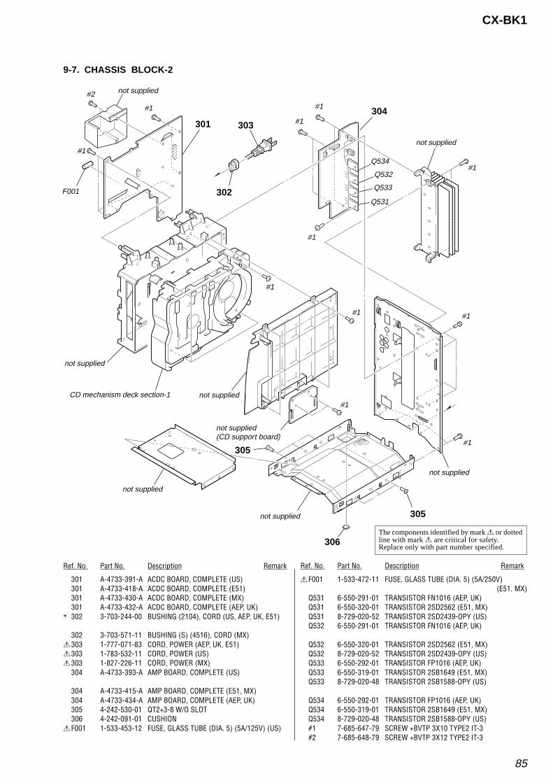
85
CX-BK1
9-7. CHASSIS BLOCK-2
305
305
304
302
301 303
306
not supplied
not supplied
not supplied
not supplied
F001
not supplied
not supplied
not supplied
Q534
Q532
Q533
Q531
not supplied(CD support board)
#1
#1
#2
#1
#1
#1
#1
#1
#1
#1
#1
#1
CD mechanism deck section-1
Ref. No. Part No. Description Remark Ref. No. Part No. Description Remark
301 A-4733-391-A ACDC BOARD, COMPLETE (US)301 A-4733-418-A ACDC BOARD, COMPLETE (E51)301 A-4733-430-A ACDC BOARD, COMPLETE (MX)301 A-4733-432-A ACDC BOARD, COMPLETE (AEP, UK)
* 302 3-703-244-00 BUSHING (2104), CORD (US, AEP, UK, E51)
302 3-703-571-11 BUSHING (S) (4516), CORD (MX)0303 1-777-071-83 CORD, POWER (AEP, UK, E51)0303 1-783-532-11 CORD, POWER (US)0303 1-827-226-11 CORD, POWER (MX)
304 A-4733-393-A AMP BOARD, COMPLETE (US)
304 A-4733-415-A AMP BOARD, COMPLETE (E51, MX)304 A-4733-434-A AMP BOARD, COMPLETE (AEP, UK)305 4-242-530-01 QT2+3-8 W/O SLOT306 4-242-091-01 CUSHION
0F001 1-533-453-12 FUSE, GLASS TUBE (DIA. 5) (5A/125V) (US)
0F001 1-533-472-11 FUSE, GLASS TUBE (DIA. 5) (5A/250V)(E51, MX)
Q531 6-550-291-01 TRANSISTOR FN1016 (AEP, UK)Q531 6-550-320-01 TRANSISTOR 2SD2562 (E51, MX)Q531 8-729-020-52 TRANSISTOR 2SD2439-OPY (US)Q532 6-550-291-01 TRANSISTOR FN1016 (AEP, UK)
Q532 6-550-320-01 TRANSISTOR 2SD2562 (E51, MX)Q532 8-729-020-52 TRANSISTOR 2SD2439-OPY (US)Q533 6-550-292-01 TRANSISTOR FP1016 (AEP, UK)Q533 6-550-319-01 TRANSISTOR 2SB1649 (E51, MX)Q533 8-729-020-48 TRANSISTOR 2SB1588-OPY (US)
Q534 6-550-292-01 TRANSISTOR FP1016 (AEP, UK)Q534 6-550-319-01 TRANSISTOR 2SB1649 (E51, MX)Q534 8-729-020-48 TRANSISTOR 2SB1588-OPY (US)#1 7-685-647-79 SCREW +BVTP 3X10 TYPE2 IT-3#2 7-685-648-79 SCREW +BVTP 3X12 TYPE2 IT-3
The components identified by mark 0 or dottedline with mark 0 are critical for safety.Replace only with part number specified.
86
CX-BK1
9-8. CD MECHANISM DECK SECTION-1 (CDM69BV-30CBD64NS)
501 1-686-725-12 STOCKER MOTOR BOARD502 4-951-620-01 SCREW (2.6X8), +BVTP503 4-239-690-01 CAM (STOCKER U/D)504 4-239-618-01 SCREW (+PWH,2X6), STEP TAPPING506 4-239-687-01 GEAR (STOCKER COMMUNICATION)
507 A-4731-113-A CONNECTOR BOARD, COMPLETE508 4-239-689-01 GEAR (STOCKER DECELERATION)
509 4-239-683-01 PULLEY (MODE DECELERATION)510 4-221-273-01 BELT (MODE)513 4-244-764-01 CAM (STOCKER V)M761 A-4735-953-A MOTOR ASSY (STOCKER)S702 1-477-299-11 ENCODER, ROTARY (STOCKER POSITION)
#4 7-685-902-21 SCREW +PTPWH 2.6X8 (TYPE2)
Ref. No. Part No. Description Remark Ref. No. Part No. Description Remark
508
502507
509
510
502
#4
506#4
501
502
513
504
M761
#4
503
#4S702
CD mechanism deck section-2
not supplied(ST encorder board)
not supplied
87
CX-BK1
9-9. CD MECHANISM DECK SECTION-2 (CDM69BV-30CBD64NS)
551 1-686-727-12 SW (1) BOARD552 1-686-728-12 SW (2) BOARD553 1-686-729-12 SW (3) BOARD554 1-686-730-12 SW (4) BOARD555 4-951-620-01 SCREW (2.6X8), +BVTP
556 4-985-672-01 SCREW (+PTPWHM 2.6), FLOATING
557 4-227-899-01 SCREW (DIA,12), FLOATING558 4-243-716-01 HOLDER (BU-30)559 4-234-824-01 RUBBER, VIBRATION PROOF560 4-985-672-01 SCREW (+PTPWHM2.6), FLOATING261 4-244-960-02 SPRING (BU30-1), TENSION
#5 7-685-533-14 SCREW +BTP 2.6X6 TYPE2 N-S
552 553 554
555
551 555
#5
optical pick-upsection
556
557
CD mechanism deck section-3
CD mechanism deck section-5
558
559
560
561
559
560
559
560
559
560
Ref. No. Part No. Description Remark Ref. No. Part No. Description Remark

88
CX-BK1
9-10. CD MECHANISM DECK SECTION-3 (CDM69BV-30CBD64NS)
605
606607
602
609
609
611
not supplied
not supplied
not supplied
614
613
622
608
not supplied
615
612
604
602
616
623617
615
618
618
602
624
602
603
604
601
621
605
620
610
not supplied
618
618
602
619
not supplied
Ref. No. Part No. Description Remark Ref. No. Part No. Description Remark
601 X-4955-447-1 PULLEY (A)(BU30) ASSY,CHUCKING602 4-992-069-01 SCREW (+PTPWH) (M2) (DIA. 7)603 4-239-648-01 PARASOL (ROLLER)604 4-239-646-01 ROLLER (ROLLER)605 4-239-641-01 SPRING (1.2), TENSION
606 4-239-642-01 SPRING (3), TENSION COIL607 4-239-679-01 SPRING (5), TENSION COIL608 4-243-714-01 PULLEY (B) (BU30), CHUCKING609 4-239-649-01 PARASOL (STOCKER)610 4-240-040-01 SPRING (DISC STOPPER), TORSION
611 4-244-035-01 ROLLER (STOCKER), RUBBER612 4-239-640-01 PINION (SLIDER)
613 4-243-291-01 SPRING, TORSION614 4-240-039-01 LEVER (DISC STOPPER)615 4-239-702-01 ROLLER (DISC STOPPER)616 4-985-672-01 SCREW (+PTPWHM2.6), FLOATING617 4-243-713-01 LEVER (LIFTER)
618 4-239-647-01 PARASOL (MAIN)619 4-243-916-01 ROLLER (S), RUBBER620 4-241-599-01 LEVER (SUPPORT)621 4-228-414-01 BRACKET (YOKE)622 4-239-643-01 SPRING (4), TENSION COIL
623 4-243-914-01 SPRING (LIFTER), TORSION624 4-244-032-01 ROLLER, RUBBER
89
CX-BK1
9-11. CD MECHANISM DECK SECTION-4 (CDM69BV-30CBD64NS)
653
654
657
657
657
657
656
655
658
658
657
667
#6
#6
#6
653
653
652
652
662
654
656
656
657
655655
654 657
657
657
656
658
#6
653
652
654
669
670
671
664
661
661
655
670
656
655
658
668
651
651
663
not supplied
#6#6
651
652
660666
661
661
665675
672
M781
673
666
CD mechanism deck section-5
Ref. No. Part No. Description Remark Ref. No. Part No. Description Remark
651 X-4954-626-1 LEVER (ROLLER) ASSY652 4-239-666-01 GEAR653 4-239-668-01 LEVER (CENTER)654 4-239-652-01 SCREW (ROLLER), STEP655 4-239-669-01 GEAR (ROLLER COMMUNICATION)
656 4-239-667-01 GEAR (ROLLER CENTER)657 4-239-647-01 PARASOL (MAIN)658 4-244-032-01 ROLLER, RUBBER660 X-4954-622-1 BASE (SLIDER 2) ASSY661 4-239-670-01 GEAR (ROLLER 5 COMMUNICATION)
662 X-4954-624-A LEVER (SLIDER 4) ASSY663 4-992-069-01 SCREW (+PTPWH)(M2)(DIA. 7)664 4-240-981-01 SPRING (BASE SLIDER 5),TENSION
665 4-240-041-01 SPRING (SLIDER 2), TENSION666 4-951-620-01 SCREW (2.6X8), +BVTP667 4-243-916-01 ROLLER (S), RUBBER668 4-244-035-01 ROLLER (STOCKER), RUBBER669 4-241-209-01 SHEET, ADHESIVE
670 4-239-649-01 PARASOL (STOCKER)671 4-239-671-01 GEAR (ROLLER 5 CENTER)672 X-4954-627-1 BASE (SLIDER 5) ASSY673 1-686-726-12 ROLLER MOTOR BOARD675 4-244-162-01 SPRING (SLIDER 4),TENSION
M781 A-4735-953-A MOTOR ASSY (ROLLER)#6 7-623-921-01 WASHER 1.7, NYLON

90
CX-BK1
9-12. CD MECHANISM DECK SECTION-5 (CDM69BV-30CBD64NS)
701702
703
703704
705
705
706
707709
708#4
CD mechanism deck section-6
Ref. No. Part No. Description Remark Ref. No. Part No. Description Remark
701 4-240-020-01 GEAR (TIMING)702 4-239-708-02 BELT (FRONT), TIMING703 4-239-697-01 GEAR (CENTER)704 X-4955-157-1 SLIDER (MODE CAM V) ASSY705 4-239-706-02 BELT (REAR), TIMING
706 4-239-699-01 PULLEY707 4-247-349-02 BELT (ROLLER V)708 4-227-899-01 SCREW (DIA. 12), FLOATING709 4-239-686-01 GEAR (ROLLER DECELERATION)#4 7-685-902-21 SCREW +PTPWH 2.6X8 (TYPE2)
91
CX-BK1
9-13. CD MECHANISM DECK SECTION-6 (CDM69BV-30CBD64NS)
758
759
763
775
751
769
770
764
754
765
753
#4
#4
#4
#4
not supplied
not suppliedM771
757762772
760
752
763763
771
763
766
767
761
#4
#4
S771#4
#4
755#4
755#4
Ref. No. Part No. Description Remark Ref. No. Part No. Description Remark
751 4-239-693-02 CAM (GEAR)752 1-686-723-12 SENSOR BOARD753 4-239-696-01 GEAR (EJECT LOCK)754 4-239-695-02 CAM (EJECT LOCK)755 4-240-019-01 GEAR (MODE 5)
757 4-243-682-01 GEAR (MODE C)758 4-239-683-01 PULLEY (MODE DECELERATION)759 4-243-702-01 BELT (MODE V)760 4-243-683-01 GEAR (MODE D)761 4-239-618-01 SCREW (+PWH,2X6), STEP TAPPING
762 4-243-681-01 GEAR (MODE B)763 4-951-620-01 SCREW (2.6X8), +BVTP
764 4-239-692-02 CAM (BU U/D)765 4-239-694-01 GEAR (MODE CAM)766 4-241-731-01 SHUTTER (A), LEVER767 4-241-732-01 SHUTTER (B), LEVER769 4-241-734-01 SHAFT (SHUTTER)
770 4-241-735-01 SPRING (SHUTTER), COMPRESSION771 4-685-672-01 SCREW (DIA. 12), FLOATING772 4-243-680-01 GEAR (MODE A)775 1-686-724-12 MODE MOTOR BOARDM771 A-4735-953-A MOTOR ASSY (MODE)
S771 1-477-300-11 ENCODER, ROTARY (MODE)#4 7-685-902-21 SCREW +PTPWH 2.6X8 (TYPE2)
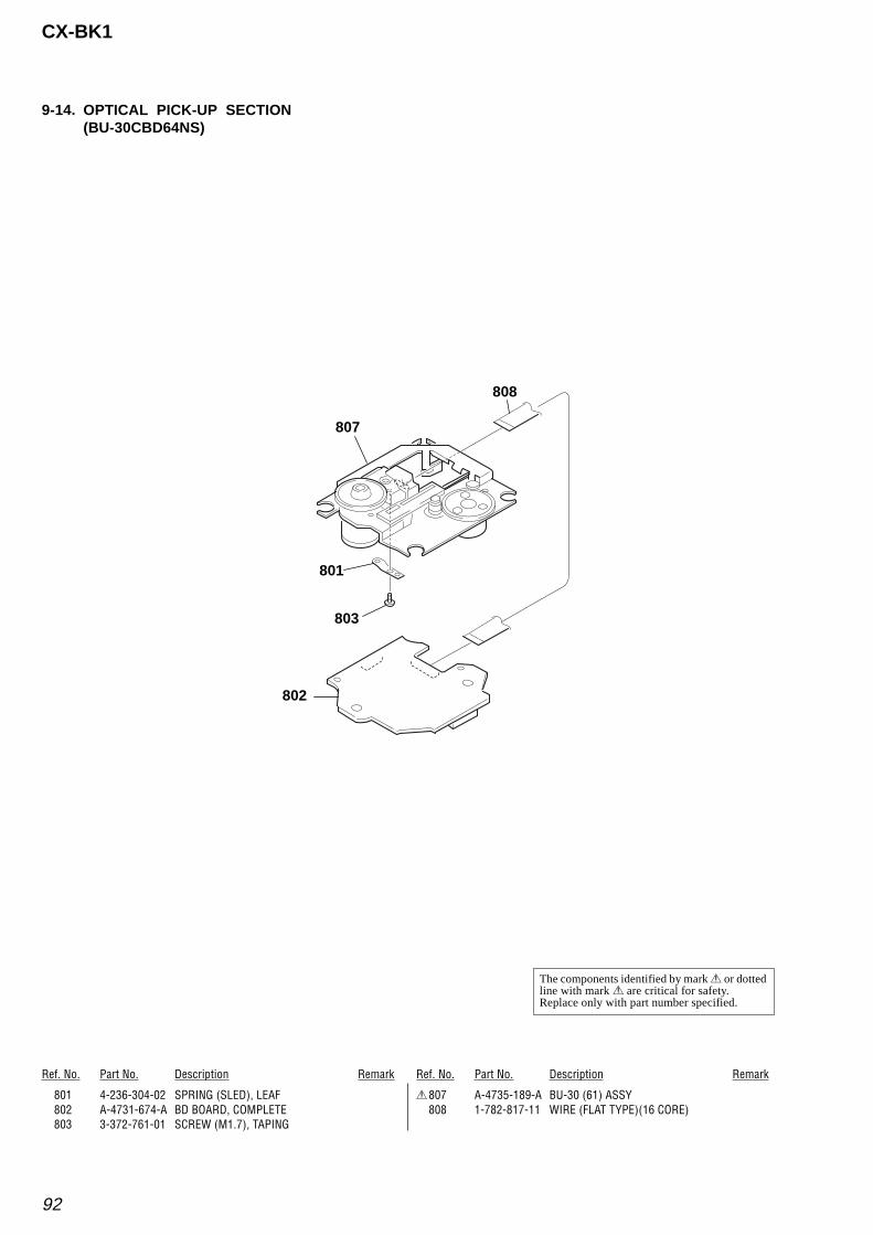
92
CX-BK1
9-14. OPTICAL PICK-UP SECTION(BU-30CBD64NS)
808
802
807
801
803
Ref. No. Part No. Description Remark Ref. No. Part No. Description Remark
801 4-236-304-02 SPRING (SLED), LEAF802 A-4731-674-A BD BOARD, COMPLETE803 3-372-761-01 SCREW (M1.7), TAPING
0807 A-4735-189-A BU-30 (61) ASSY808 1-782-817-11 WIRE (FLAT TYPE)(16 CORE)
The components identified by mark 0 or dottedline with mark 0 are critical for safety.Replace only with part number specified.
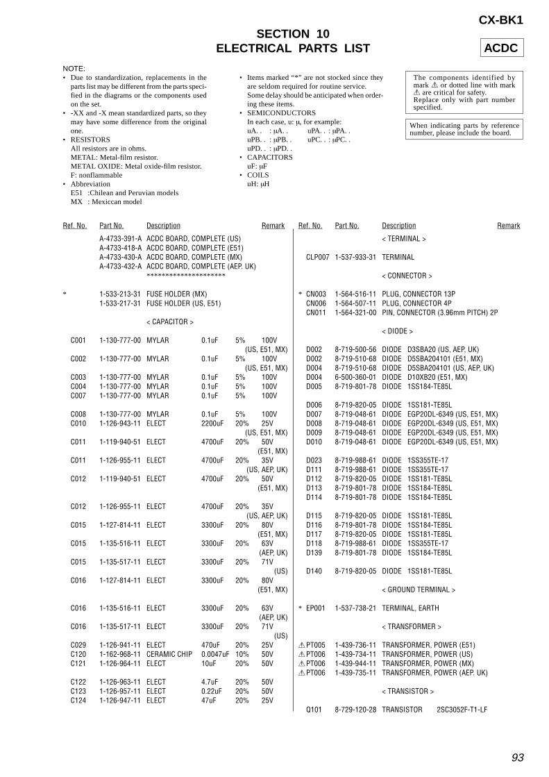
93
CX-BK1SECTION 10
ELECTRICAL PARTS LIST
Ref. No. Part No. Description Remark Ref. No. Part No. Description Remark
ACDC
A-4733-391-A ACDC BOARD, COMPLETE (US)A-4733-418-A ACDC BOARD, COMPLETE (E51)A-4733-430-A ACDC BOARD, COMPLETE (MX)A-4733-432-A ACDC BOARD, COMPLETE (AEP. UK)
*********************
* 1-533-213-31 FUSE HOLDER (MX)1-533-217-31 FUSE HOLDER (US, E51)
< CAPACITOR >
C001 1-130-777-00 MYLAR 0.1uF 5% 100V(US, E51, MX)
C002 1-130-777-00 MYLAR 0.1uF 5% 100V(US, E51, MX)
C003 1-130-777-00 MYLAR 0.1uF 5% 100VC004 1-130-777-00 MYLAR 0.1uF 5% 100VC007 1-130-777-00 MYLAR 0.1uF 5% 100V
C008 1-130-777-00 MYLAR 0.1uF 5% 100VC010 1-126-943-11 ELECT 2200uF 20% 25V
(US, E51, MX)C011 1-119-940-51 ELECT 4700uF 20% 50V
(E51, MX)C011 1-126-955-11 ELECT 4700uF 20% 35V
(US, AEP, UK)C012 1-119-940-51 ELECT 4700uF 20% 50V
(E51, MX)
C012 1-126-955-11 ELECT 4700uF 20% 35V(US, AEP, UK)
C015 1-127-814-11 ELECT 3300uF 20% 80V(E51, MX)
C015 1-135-516-11 ELECT 3300uF 20% 63V(AEP, UK)
C015 1-135-517-11 ELECT 3300uF 20% 71V(US)
C016 1-127-814-11 ELECT 3300uF 20% 80V(E51, MX)
C016 1-135-516-11 ELECT 3300uF 20% 63V(AEP, UK)
C016 1-135-517-11 ELECT 3300uF 20% 71V(US)
C029 1-126-941-11 ELECT 470uF 20% 25VC120 1-162-968-11 CERAMIC CHIP 0.0047uF 10% 50VC121 1-126-964-11 ELECT 10uF 20% 50V
C122 1-126-963-11 ELECT 4.7uF 20% 50VC123 1-126-957-11 ELECT 0.22uF 20% 50VC124 1-126-947-11 ELECT 47uF 20% 25V
NOTE:• Due to standardization, replacements in the
parts list may be different from the parts speci-fied in the diagrams or the components usedon the set.
• -XX and -X mean standardized parts, so theymay have some difference from the originalone.
• RESISTORSAll resistors are in ohms.METAL: Metal-film resistor.METAL OXIDE: Metal oxide-film resistor.F: nonflammable
• Items marked “*” are not stocked since theyare seldom required for routine service.Some delay should be anticipated when order-ing these items.
• SEMICONDUCTORSIn each case, u: µ, for example:uA. . : µA. . uPA. . : µPA. .uPB. . : µPB. . uPC. . : µPC. .uPD. . : µPD. .
• CAPACITORSuF: µF
• COILSuH: µH
< TERMINAL >
CLP007 1-537-933-31 TERMINAL
< CONNECTOR >
* CN003 1-564-516-11 PLUG, CONNECTOR 13PCN006 1-564-507-11 PLUG, CONNECTOR 4PCN011 1-564-321-00 PIN, CONNECTOR (3.96mm PITCH) 2P
< DIODE >
D002 8-719-500-56 DIODE D3SBA20 (US, AEP, UK)D002 8-719-510-68 DIODE D5SBA204101 (E51, MX)D004 8-719-510-68 DIODE D5SBA204101 (US, AEP, UK)D004 6-500-360-01 DIODE D10XB20 (E51, MX)D005 8-719-801-78 DIODE 1SS184-TE85L
D006 8-719-820-05 DIODE 1SS181-TE85LD007 8-719-048-61 DIODE EGP20DL-6349 (US, E51, MX)D008 8-719-048-61 DIODE EGP20DL-6349 (US, E51, MX)D009 8-719-048-61 DIODE EGP20DL-6349 (US, E51, MX)D010 8-719-048-61 DIODE EGP20DL-6349 (US, E51, MX)
D023 8-719-988-61 DIODE 1SS355TE-17D111 8-719-988-61 DIODE 1SS355TE-17D112 8-719-820-05 DIODE 1SS181-TE85LD113 8-719-801-78 DIODE 1SS184-TE85LD114 8-719-801-78 DIODE 1SS184-TE85L
D115 8-719-820-05 DIODE 1SS181-TE85LD116 8-719-801-78 DIODE 1SS184-TE85LD117 8-719-820-05 DIODE 1SS181-TE85LD118 8-719-988-61 DIODE 1SS355TE-17D139 8-719-801-78 DIODE 1SS184-TE85L
D140 8-719-820-05 DIODE 1SS181-TE85L
< GROUND TERMINAL >
* EP001 1-537-738-21 TERMINAL, EARTH
< TRANSFORMER >
0PT005 1-439-736-11 TRANSFORMER, POWER (E51)0PT006 1-439-734-11 TRANSFORMER, POWER (US)0PT006 1-439-944-11 TRANSFORMER, POWER (MX)0PT006 1-439-735-11 TRANSFORMER, POWER (AEP. UK)
< TRANSISTOR >
Q101 8-729-120-28 TRANSISTOR 2SC3052F-T1-LF
The components identified bymark 0 or dotted line with mark0 are critical for safety.Replace only with part numberspecified.
• AbbreviationE51 :Chilean and Peruvian modelsMX : Mexiccan model
When indicating parts by referencenumber, please include the board.
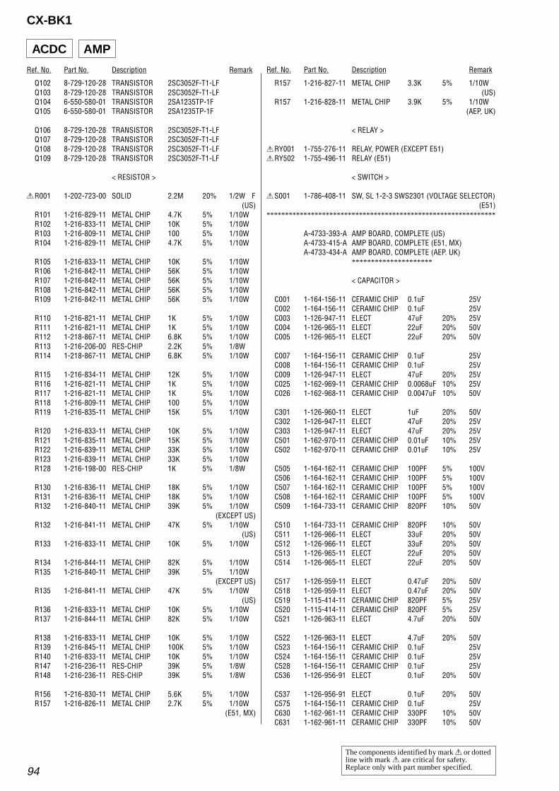
Ref. No. Part No. Description Remark Ref. No. Part No. Description Remark
94
CX-BK1
ACDC AMP
Q102 8-729-120-28 TRANSISTOR 2SC3052F-T1-LFQ103 8-729-120-28 TRANSISTOR 2SC3052F-T1-LFQ104 6-550-580-01 TRANSISTOR 2SA1235TP-1FQ105 6-550-580-01 TRANSISTOR 2SA1235TP-1F
Q106 8-729-120-28 TRANSISTOR 2SC3052F-T1-LFQ107 8-729-120-28 TRANSISTOR 2SC3052F-T1-LFQ108 8-729-120-28 TRANSISTOR 2SC3052F-T1-LFQ109 8-729-120-28 TRANSISTOR 2SC3052F-T1-LF
< RESISTOR >
0R001 1-202-723-00 SOLID 2.2M 20% 1/2W F(US)
R101 1-216-829-11 METAL CHIP 4.7K 5% 1/10WR102 1-216-833-11 METAL CHIP 10K 5% 1/10WR103 1-216-809-11 METAL CHIP 100 5% 1/10WR104 1-216-829-11 METAL CHIP 4.7K 5% 1/10W
R105 1-216-833-11 METAL CHIP 10K 5% 1/10WR106 1-216-842-11 METAL CHIP 56K 5% 1/10WR107 1-216-842-11 METAL CHIP 56K 5% 1/10WR108 1-216-842-11 METAL CHIP 56K 5% 1/10WR109 1-216-842-11 METAL CHIP 56K 5% 1/10W
R110 1-216-821-11 METAL CHIP 1K 5% 1/10WR111 1-216-821-11 METAL CHIP 1K 5% 1/10WR112 1-218-867-11 METAL CHIP 6.8K 5% 1/10WR113 1-216-206-00 RES-CHIP 2.2K 5% 1/8WR114 1-218-867-11 METAL CHIP 6.8K 5% 1/10W
R115 1-216-834-11 METAL CHIP 12K 5% 1/10WR116 1-216-821-11 METAL CHIP 1K 5% 1/10WR117 1-216-821-11 METAL CHIP 1K 5% 1/10WR118 1-216-809-11 METAL CHIP 100 5% 1/10WR119 1-216-835-11 METAL CHIP 15K 5% 1/10W
R120 1-216-833-11 METAL CHIP 10K 5% 1/10WR121 1-216-835-11 METAL CHIP 15K 5% 1/10WR122 1-216-839-11 METAL CHIP 33K 5% 1/10WR123 1-216-839-11 METAL CHIP 33K 5% 1/10WR128 1-216-198-00 RES-CHIP 1K 5% 1/8W
R130 1-216-836-11 METAL CHIP 18K 5% 1/10WR131 1-216-836-11 METAL CHIP 18K 5% 1/10WR132 1-216-840-11 METAL CHIP 39K 5% 1/10W
(EXCEPT US)R132 1-216-841-11 METAL CHIP 47K 5% 1/10W
(US)R133 1-216-833-11 METAL CHIP 10K 5% 1/10W
R134 1-216-844-11 METAL CHIP 82K 5% 1/10WR135 1-216-840-11 METAL CHIP 39K 5% 1/10W
(EXCEPT US)R135 1-216-841-11 METAL CHIP 47K 5% 1/10W
(US)R136 1-216-833-11 METAL CHIP 10K 5% 1/10WR137 1-216-844-11 METAL CHIP 82K 5% 1/10W
R138 1-216-833-11 METAL CHIP 10K 5% 1/10WR139 1-216-845-11 METAL CHIP 100K 5% 1/10WR140 1-216-833-11 METAL CHIP 10K 5% 1/10WR147 1-216-236-11 RES-CHIP 39K 5% 1/8WR148 1-216-236-11 RES-CHIP 39K 5% 1/8W
R156 1-216-830-11 METAL CHIP 5.6K 5% 1/10WR157 1-216-826-11 METAL CHIP 2.7K 5% 1/10W
(E51, MX)
R157 1-216-827-11 METAL CHIP 3.3K 5% 1/10W(US)
R157 1-216-828-11 METAL CHIP 3.9K 5% 1/10W(AEP, UK)
< RELAY >
0RY001 1-755-276-11 RELAY, POWER (EXCEPT E51)0RY502 1-755-496-11 RELAY (E51)
< SWITCH >
0S001 1-786-408-11 SW, SL 1-2-3 SWS2301 (VOLTAGE SELECTOR)(E51)
**************************************************************
A-4733-393-A AMP BOARD, COMPLETE (US)A-4733-415-A AMP BOARD, COMPLETE (E51, MX)A-4733-434-A AMP BOARD, COMPLETE (AEP. UK)
*********************
< CAPACITOR >
C001 1-164-156-11 CERAMIC CHIP 0.1uF 25VC002 1-164-156-11 CERAMIC CHIP 0.1uF 25VC003 1-126-947-11 ELECT 47uF 20% 25VC004 1-126-965-11 ELECT 22uF 20% 50VC005 1-126-965-11 ELECT 22uF 20% 50V
C007 1-164-156-11 CERAMIC CHIP 0.1uF 25VC008 1-164-156-11 CERAMIC CHIP 0.1uF 25VC009 1-126-947-11 ELECT 47uF 20% 25VC025 1-162-969-11 CERAMIC CHIP 0.0068uF 10% 25VC026 1-162-968-11 CERAMIC CHIP 0.0047uF 10% 50V
C301 1-126-960-11 ELECT 1uF 20% 50VC302 1-126-947-11 ELECT 47uF 20% 25VC303 1-126-947-11 ELECT 47uF 20% 25VC501 1-162-970-11 CERAMIC CHIP 0.01uF 10% 25VC502 1-162-970-11 CERAMIC CHIP 0.01uF 10% 25V
C505 1-164-162-11 CERAMIC CHIP 100PF 5% 100VC506 1-164-162-11 CERAMIC CHIP 100PF 5% 100VC507 1-164-162-11 CERAMIC CHIP 100PF 5% 100VC508 1-164-162-11 CERAMIC CHIP 100PF 5% 100VC509 1-164-733-11 CERAMIC CHIP 820PF 10% 50V
C510 1-164-733-11 CERAMIC CHIP 820PF 10% 50VC511 1-126-966-11 ELECT 33uF 20% 50VC512 1-126-966-11 ELECT 33uF 20% 50VC513 1-126-965-11 ELECT 22uF 20% 50VC514 1-126-965-11 ELECT 22uF 20% 50V
C517 1-126-959-11 ELECT 0.47uF 20% 50VC518 1-126-959-11 ELECT 0.47uF 20% 50VC519 1-115-414-11 CERAMIC CHIP 820PF 5% 25VC520 1-115-414-11 CERAMIC CHIP 820PF 5% 25VC521 1-126-963-11 ELECT 4.7uF 20% 50V
C522 1-126-963-11 ELECT 4.7uF 20% 50VC523 1-164-156-11 CERAMIC CHIP 0.1uF 25VC524 1-164-156-11 CERAMIC CHIP 0.1uF 25VC528 1-164-156-11 CERAMIC CHIP 0.1uF 25VC536 1-126-956-91 ELECT 0.1uF 20% 50V
C537 1-126-956-91 ELECT 0.1uF 20% 50VC575 1-164-156-11 CERAMIC CHIP 0.1uF 25VC630 1-162-961-11 CERAMIC CHIP 330PF 10% 50VC631 1-162-961-11 CERAMIC CHIP 330PF 10% 50V
The components identified by mark 0 or dottedline with mark 0 are critical for safety.Replace only with part number specified.
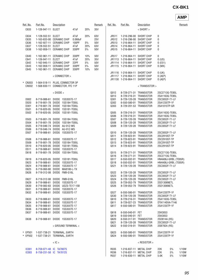
Ref. No. Part No. Description Remark Ref. No. Part No. Description Remark
95
CX-BK1
C633 1-126-947-11 ELECT 47uF 20% 35V
C634 1-128-552-51 ELECT 47uF 20% 63VC635 1-163-833-00 CERAMIC CHIP 0.068uF 25VC636 1-162-927-11 CERAMIC CHIP 100PF 5% 50VC637 1-128-552-51 ELECT 47uF 20% 63VC638 1-162-959-11 CERAMIC CHIP 330PF 5% 50V
C640 1-162-961-11 CERAMIC CHIP 330PF 10% 50VC641 1-126-947-11 ELECT 47uF 20% 35VC642 1-162-945-11 CERAMIC CHIP 22PF 5% 50VC643 1-162-959-11 CERAMIC CHIP 330PF 5% 50VC645 1-162-961-11 CERAMIC CHIP 330PF 10% 50V
< CONNECTOR >
* CN303 1-564-518-11 PLUG, CONNECTOR 3PCN502 1-568-830-11 CONNECTOR, FFC 11P
< DIODE >
D002 8-719-988-61 DIODE 1SS355TE-17D020 8-719-801-78 DIODE 1SS184-TE85LD301 8-719-801-78 DIODE 1SS184-TE85LD501 8-719-820-05 DIODE 1SS181-TE85LD502 8-719-820-05 DIODE 1SS181-TE85L
D503 8-719-801-78 DIODE 1SS184-TE85LD504 8-719-801-78 DIODE 1SS184-TE85LD505 8-719-046-74 DIODE AU-01Z-WSD506 8-719-046-74 DIODE AU-01Z-WSD507 8-719-988-61 DIODE 1SS355TE-17
D508 8-719-988-61 DIODE 1SS355TE-17D509 8-719-801-78 DIODE 1SS184-TE85LD510 8-719-820-05 DIODE 1SS181-TE85LD511 8-719-988-61 DIODE 1SS355TE-17D618 8-719-801-78 DIODE 1SS184-TE85L
D619 8-719-820-05 DIODE 1SS181-TE85LD623 8-719-988-61 DIODE 1SS355TE-17D624 8-719-988-61 DIODE 1SS355TE-17D625 8-719-060-80 DIODE MA8180-L-TXD626 8-719-312-08 DIODE FMB-G16L
D627 8-719-312-08 DIODE FMB-G16LD629 8-719-988-61 DIODE 1SS355TE-17D630 8-719-083-83 DIODE UDZS-TE17-15BD631 8-719-988-61 DIODE 1SS355TE-17D632 8-719-988-61 DIODE 1SS355TE-17
D633 8-719-988-61 DIODE 1SS355TE-17D634 8-719-988-61 DIODE 1SS355TE-17D635 8-719-988-61 DIODE 1SS355TE-17D636 8-719-988-61 DIODE 1SS355TE-17D637 8-719-988-61 DIODE 1SS355TE-17
D638 8-719-988-61 DIODE 1SS355TE-17
< GROUND TERMINAL >
* EP501 1-537-738-21 TERMINAL, EARTH* EP502 1-537-738-21 TERMINAL, EARTH
< IC >
IC001 8-759-071-48 IC TA7807SIC003 8-759-231-58 IC TA7812S
< SHORT >
JR511 1-216-296-00 SHORT CHIP 0JR512 1-216-296-00 SHORT CHIP 0JR513 1-216-864-11 SHORT CHIP 0JR514 1-216-864-11 SHORT CHIP 0JR515 1-216-864-11 SHORT CHIP 0
JR517 1-216-864-11 SHORT CHIP 0JR1113 1-216-864-11 SHORT CHIP 0 (US)JR1114 1-216-864-11 SHORT CHIP 0 (E51)JR1115 1-216-864-11 SHORT CHIP 0 (MX)
JR1116 1-216-864-11 SHORT CHIP 0 (UK)JR1117 1-216-864-11 SHORT CHIP 0 (AEP)JR1130 1-216-864-11 SHORT CHIP 0 (AEP)
< TRANSISTOR >
Q012 8-729-271-31 TRANSISTOR 2SC2713G-TE85LQ013 8-729-216-31 TRANSISTOR 2SA1163G-TE85LQ301 8-729-120-28 TRANSISTOR 2SC3052F-T1-LFQ302 6-550-580-01 TRANSISTOR 2SA1235TP-1FQ303 8-729-201-53 TRANSISTOR 2SA1015TP-GR
Q505 8-729-216-31 TRANSISTOR 2SA1163G-TE85LQ506 8-729-216-31 TRANSISTOR 2SA1163G-TE85LQ507 8-729-120-28 TRANSISTOR 2SC3052F-T1-LFQ508 8-729-120-28 TRANSISTOR 2SC3052F-T1-LFQ509 8-729-120-28 TRANSISTOR 2SC3052F-T1-LF
Q510 8-729-120-28 TRANSISTOR 2SC3052F-T1-LFQ511 8-729-823-91 TRANSISTOR 2SC2910ST-TPQ512 8-729-823-91 TRANSISTOR 2SC2910ST-TPQ513 8-729-823-91 TRANSISTOR 2SC2910ST-TPQ514 8-729-823-91 TRANSISTOR 2SC2910ST-TP
Q515 8-729-271-31 TRANSISTOR 2SC2713G-TE85LQ516 8-729-271-31 TRANSISTOR 2SC2713G-TE85LQ517 6-550-032-01 TRANSISTOR HN4A06J-GRBL (TE85R)Q518 6-550-032-01 TRANSISTOR HN4A06J-GRBL (TE85R)Q521 8-729-120-28 TRANSISTOR 2SC3052F-T1-LF
Q522 8-729-120-28 TRANSISTOR 2SC3052F-T1-LFQ523 8-729-120-28 TRANSISTOR 2SC3052F-T1-LFQ524 8-729-120-28 TRANSISTOR 2SC3052F-T1-LFQ525 8-729-052-79 TRANSISTOR 2SD1306NETLQ526 8-729-052-79 TRANSISTOR 2SD1306NETL
Q527 6-550-580-01 TRANSISTOR 2SA1235TP-1FQ530 8-729-120-28 TRANSISTOR 2SC3052F-T1-LFQ610 8-729-216-31 TRANSISTOR 2SA1163G-TE85LQ611 8-729-027-23 TRANSISTOR DTA114EKA-T146Q617 6-550-580-01 TRANSISTOR 2SA1235TP-1F
Q618 6-550-040-01 FET 2SK3053Q619 6-550-040-01 FET 2SK3053Q620 6-550-317-01 TRANSISTOR 2SD814A (RS)Q621 8-729-120-28 TRANSISTOR 2SC3052F-T1-LFQ622 6-550-316-01 TRANSISTOR 2SB792A (RS)
Q623 6-550-580-01 TRANSISTOR 2SA1235TP-1FQ624 6-550-580-01 TRANSISTOR 2SA1235TP-1F
< RESISTOR >
R035 1-216-837-11 METAL CHIP 22K 5% 1/10WR036 1-216-837-11 METAL CHIP 22K 5% 1/10WR037 1-216-830-11 METAL CHIP 5.6K 5% 1/10W
AMP
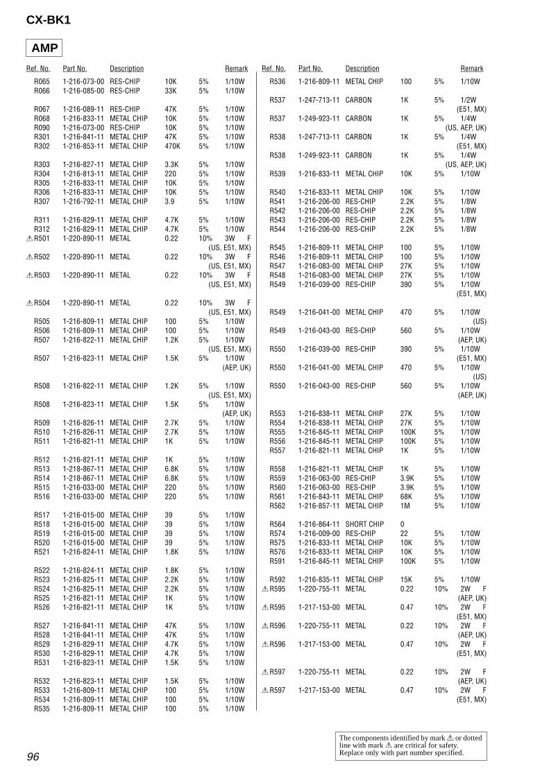
Ref. No. Part No. Description Remark Ref. No. Part No. Description Remark
96
CX-BK1
R065 1-216-073-00 RES-CHIP 10K 5% 1/10WR066 1-216-085-00 RES-CHIP 33K 5% 1/10W
R067 1-216-089-11 RES-CHIP 47K 5% 1/10WR068 1-216-833-11 METAL CHIP 10K 5% 1/10WR090 1-216-073-00 RES-CHIP 10K 5% 1/10WR301 1-216-841-11 METAL CHIP 47K 5% 1/10WR302 1-216-853-11 METAL CHIP 470K 5% 1/10W
R303 1-216-827-11 METAL CHIP 3.3K 5% 1/10WR304 1-216-813-11 METAL CHIP 220 5% 1/10WR305 1-216-833-11 METAL CHIP 10K 5% 1/10WR306 1-216-833-11 METAL CHIP 10K 5% 1/10WR307 1-216-792-11 METAL CHIP 3.9 5% 1/10W
R311 1-216-829-11 METAL CHIP 4.7K 5% 1/10WR312 1-216-829-11 METAL CHIP 4.7K 5% 1/10W
0R501 1-220-890-11 METAL 0.22 10% 3W F(US, E51, MX)
0R502 1-220-890-11 METAL 0.22 10% 3W F(US, E51, MX)
0R503 1-220-890-11 METAL 0.22 10% 3W F(US, E51, MX)
0R504 1-220-890-11 METAL 0.22 10% 3W F(US, E51, MX)
R505 1-216-809-11 METAL CHIP 100 5% 1/10WR506 1-216-809-11 METAL CHIP 100 5% 1/10WR507 1-216-822-11 METAL CHIP 1.2K 5% 1/10W
(US, E51, MX)R507 1-216-823-11 METAL CHIP 1.5K 5% 1/10W
(AEP, UK)
R508 1-216-822-11 METAL CHIP 1.2K 5% 1/10W(US, E51, MX)
R508 1-216-823-11 METAL CHIP 1.5K 5% 1/10W(AEP, UK)
R509 1-216-826-11 METAL CHIP 2.7K 5% 1/10WR510 1-216-826-11 METAL CHIP 2.7K 5% 1/10WR511 1-216-821-11 METAL CHIP 1K 5% 1/10W
R512 1-216-821-11 METAL CHIP 1K 5% 1/10WR513 1-218-867-11 METAL CHIP 6.8K 5% 1/10WR514 1-218-867-11 METAL CHIP 6.8K 5% 1/10WR515 1-216-033-00 METAL CHIP 220 5% 1/10WR516 1-216-033-00 METAL CHIP 220 5% 1/10W
R517 1-216-015-00 METAL CHIP 39 5% 1/10WR518 1-216-015-00 METAL CHIP 39 5% 1/10WR519 1-216-015-00 METAL CHIP 39 5% 1/10WR520 1-216-015-00 METAL CHIP 39 5% 1/10WR521 1-216-824-11 METAL CHIP 1.8K 5% 1/10W
R522 1-216-824-11 METAL CHIP 1.8K 5% 1/10WR523 1-216-825-11 METAL CHIP 2.2K 5% 1/10WR524 1-216-825-11 METAL CHIP 2.2K 5% 1/10WR525 1-216-821-11 METAL CHIP 1K 5% 1/10WR526 1-216-821-11 METAL CHIP 1K 5% 1/10W
R527 1-216-841-11 METAL CHIP 47K 5% 1/10WR528 1-216-841-11 METAL CHIP 47K 5% 1/10WR529 1-216-829-11 METAL CHIP 4.7K 5% 1/10WR530 1-216-829-11 METAL CHIP 4.7K 5% 1/10WR531 1-216-823-11 METAL CHIP 1.5K 5% 1/10W
R532 1-216-823-11 METAL CHIP 1.5K 5% 1/10WR533 1-216-809-11 METAL CHIP 100 5% 1/10WR534 1-216-809-11 METAL CHIP 100 5% 1/10WR535 1-216-809-11 METAL CHIP 100 5% 1/10W
R536 1-216-809-11 METAL CHIP 100 5% 1/10W
R537 1-247-713-11 CARBON 1K 5% 1/2W(E51, MX)
R537 1-249-923-11 CARBON 1K 5% 1/4W(US, AEP, UK)
R538 1-247-713-11 CARBON 1K 5% 1/4W(E51, MX)
R538 1-249-923-11 CARBON 1K 5% 1/4W(US, AEP, UK)
R539 1-216-833-11 METAL CHIP 10K 5% 1/10W
R540 1-216-833-11 METAL CHIP 10K 5% 1/10WR541 1-216-206-00 RES-CHIP 2.2K 5% 1/8WR542 1-216-206-00 RES-CHIP 2.2K 5% 1/8WR543 1-216-206-00 RES-CHIP 2.2K 5% 1/8WR544 1-216-206-00 RES-CHIP 2.2K 5% 1/8W
R545 1-216-809-11 METAL CHIP 100 5% 1/10WR546 1-216-809-11 METAL CHIP 100 5% 1/10WR547 1-216-083-00 METAL CHIP 27K 5% 1/10WR548 1-216-083-00 METAL CHIP 27K 5% 1/10WR549 1-216-039-00 RES-CHIP 390 5% 1/10W
(E51, MX)
R549 1-216-041-00 METAL CHIP 470 5% 1/10W(US)
R549 1-216-043-00 RES-CHIP 560 5% 1/10W (AEP, UK)
R550 1-216-039-00 RES-CHIP 390 5% 1/10W(E51, MX)
R550 1-216-041-00 METAL CHIP 470 5% 1/10W(US)
R550 1-216-043-00 RES-CHIP 560 5% 1/10W(AEP, UK)
R553 1-216-838-11 METAL CHIP 27K 5% 1/10WR554 1-216-838-11 METAL CHIP 27K 5% 1/10WR555 1-216-845-11 METAL CHIP 100K 5% 1/10WR556 1-216-845-11 METAL CHIP 100K 5% 1/10WR557 1-216-821-11 METAL CHIP 1K 5% 1/10W
R558 1-216-821-11 METAL CHIP 1K 5% 1/10WR559 1-216-063-00 RES-CHIP 3.9K 5% 1/10WR560 1-216-063-00 RES-CHIP 3.9K 5% 1/10WR561 1-216-843-11 METAL CHIP 68K 5% 1/10WR562 1-216-857-11 METAL CHIP 1M 5% 1/10W
R564 1-216-864-11 SHORT CHIP 0R574 1-216-009-00 RES-CHIP 22 5% 1/10WR575 1-216-833-11 METAL CHIP 10K 5% 1/10WR576 1-216-833-11 METAL CHIP 10K 5% 1/10WR591 1-216-845-11 METAL CHIP 100K 5% 1/10W
R592 1-216-835-11 METAL CHIP 15K 5% 1/10W0R595 1-220-755-11 METAL 0.22 10% 2W F
(AEP, UK)0R595 1-217-153-00 METAL 0.47 10% 2W F
(E51, MX)0R596 1-220-755-11 METAL 0.22 10% 2W F
(AEP, UK)0R596 1-217-153-00 METAL 0.47 10% 2W F
(E51, MX)
0R597 1-220-755-11 METAL 0.22 10% 2W F(AEP, UK)
0R597 1-217-153-00 METAL 0.47 10% 2W F(E51, MX)
AMP
The components identified by mark 0 or dottedline with mark 0 are critical for safety.Replace only with part number specified.
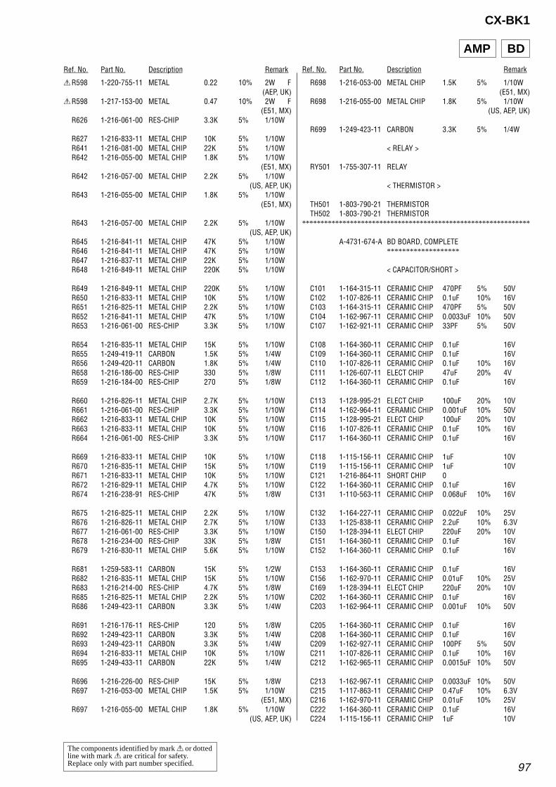
Ref. No. Part No. Description Remark Ref. No. Part No. Description Remark
97
CX-BK1
0R598 1-220-755-11 METAL 0.22 10% 2W F(AEP, UK)
0R598 1-217-153-00 METAL 0.47 10% 2W F(E51, MX)
R626 1-216-061-00 RES-CHIP 3.3K 5% 1/10W
R627 1-216-833-11 METAL CHIP 10K 5% 1/10WR641 1-216-081-00 METAL CHIP 22K 5% 1/10WR642 1-216-055-00 METAL CHIP 1.8K 5% 1/10W
(E51, MX)R642 1-216-057-00 METAL CHIP 2.2K 5% 1/10W
(US, AEP, UK)R643 1-216-055-00 METAL CHIP 1.8K 5% 1/10W
(E51, MX)
R643 1-216-057-00 METAL CHIP 2.2K 5% 1/10W(US, AEP, UK)
R645 1-216-841-11 METAL CHIP 47K 5% 1/10WR646 1-216-841-11 METAL CHIP 47K 5% 1/10WR647 1-216-837-11 METAL CHIP 22K 5% 1/10WR648 1-216-849-11 METAL CHIP 220K 5% 1/10W
R649 1-216-849-11 METAL CHIP 220K 5% 1/10WR650 1-216-833-11 METAL CHIP 10K 5% 1/10WR651 1-216-825-11 METAL CHIP 2.2K 5% 1/10WR652 1-216-841-11 METAL CHIP 47K 5% 1/10WR653 1-216-061-00 RES-CHIP 3.3K 5% 1/10W
R654 1-216-835-11 METAL CHIP 15K 5% 1/10WR655 1-249-419-11 CARBON 1.5K 5% 1/4WR656 1-249-420-11 CARBON 1.8K 5% 1/4WR658 1-216-186-00 RES-CHIP 330 5% 1/8WR659 1-216-184-00 RES-CHIP 270 5% 1/8W
R660 1-216-826-11 METAL CHIP 2.7K 5% 1/10WR661 1-216-061-00 RES-CHIP 3.3K 5% 1/10WR662 1-216-833-11 METAL CHIP 10K 5% 1/10WR663 1-216-833-11 METAL CHIP 10K 5% 1/10WR664 1-216-061-00 RES-CHIP 3.3K 5% 1/10W
R669 1-216-833-11 METAL CHIP 10K 5% 1/10WR670 1-216-835-11 METAL CHIP 15K 5% 1/10WR671 1-216-833-11 METAL CHIP 10K 5% 1/10WR672 1-216-829-11 METAL CHIP 4.7K 5% 1/10WR674 1-216-238-91 RES-CHIP 47K 5% 1/8W
R675 1-216-825-11 METAL CHIP 2.2K 5% 1/10WR676 1-216-826-11 METAL CHIP 2.7K 5% 1/10WR677 1-216-061-00 RES-CHIP 3.3K 5% 1/10WR678 1-216-234-00 RES-CHIP 33K 5% 1/8WR679 1-216-830-11 METAL CHIP 5.6K 5% 1/10W
R681 1-259-583-11 CARBON 15K 5% 1/2WR682 1-216-835-11 METAL CHIP 15K 5% 1/10WR683 1-216-214-00 RES-CHIP 4.7K 5% 1/8WR685 1-216-825-11 METAL CHIP 2.2K 5% 1/10WR686 1-249-423-11 CARBON 3.3K 5% 1/4W
R691 1-216-176-11 RES-CHIP 120 5% 1/8WR692 1-249-423-11 CARBON 3.3K 5% 1/4WR693 1-249-423-11 CARBON 3.3K 5% 1/4WR694 1-216-833-11 METAL CHIP 10K 5% 1/10WR695 1-249-433-11 CARBON 22K 5% 1/4W
R696 1-216-226-00 RES-CHIP 15K 5% 1/8WR697 1-216-053-00 METAL CHIP 1.5K 5% 1/10W
(E51, MX)R697 1-216-055-00 METAL CHIP 1.8K 5% 1/10W
(US, AEP, UK)
R698 1-216-053-00 METAL CHIP 1.5K 5% 1/10W(E51, MX)
R698 1-216-055-00 METAL CHIP 1.8K 5% 1/10W(US, AEP, UK)
R699 1-249-423-11 CARBON 3.3K 5% 1/4W
< RELAY >
RY501 1-755-307-11 RELAY
< THERMISTOR >
TH501 1-803-790-21 THERMISTORTH502 1-803-790-21 THERMISTOR
**************************************************************
A-4731-674-A BD BOARD, COMPLETE*******************
< CAPACITOR/SHORT >
C101 1-164-315-11 CERAMIC CHIP 470PF 5% 50VC102 1-107-826-11 CERAMIC CHIP 0.1uF 10% 16VC103 1-164-315-11 CERAMIC CHIP 470PF 5% 50VC104 1-162-967-11 CERAMIC CHIP 0.0033uF 10% 50VC107 1-162-921-11 CERAMIC CHIP 33PF 5% 50V
C108 1-164-360-11 CERAMIC CHIP 0.1uF 16VC109 1-164-360-11 CERAMIC CHIP 0.1uF 16VC110 1-107-826-11 CERAMIC CHIP 0.1uF 10% 16VC111 1-126-607-11 ELECT CHIP 47uF 20% 4VC112 1-164-360-11 CERAMIC CHIP 0.1uF 16V
C113 1-128-995-21 ELECT CHIP 100uF 20% 10VC114 1-162-964-11 CERAMIC CHIP 0.001uF 10% 50VC115 1-128-995-21 ELECT CHIP 100uF 20% 10VC116 1-107-826-11 CERAMIC CHIP 0.1uF 10% 16VC117 1-164-360-11 CERAMIC CHIP 0.1uF 16V
C118 1-115-156-11 CERAMIC CHIP 1uF 10VC119 1-115-156-11 CERAMIC CHIP 1uF 10VC121 1-216-864-11 SHORT CHIP 0C122 1-164-360-11 CERAMIC CHIP 0.1uF 16VC131 1-110-563-11 CERAMIC CHIP 0.068uF 10% 16V
C132 1-164-227-11 CERAMIC CHIP 0.022uF 10% 25VC133 1-125-838-11 CERAMIC CHIP 2.2uF 10% 6.3VC150 1-128-394-11 ELECT CHIP 220uF 20% 10VC151 1-164-360-11 CERAMIC CHIP 0.1uF 16VC152 1-164-360-11 CERAMIC CHIP 0.1uF 16V
C153 1-164-360-11 CERAMIC CHIP 0.1uF 16VC156 1-162-970-11 CERAMIC CHIP 0.01uF 10% 25VC169 1-128-394-11 ELECT CHIP 220uF 20% 10VC202 1-164-360-11 CERAMIC CHIP 0.1uF 16VC203 1-162-964-11 CERAMIC CHIP 0.001uF 10% 50V
C205 1-164-360-11 CERAMIC CHIP 0.1uF 16VC208 1-164-360-11 CERAMIC CHIP 0.1uF 16VC209 1-162-927-11 CERAMIC CHIP 100PF 5% 50VC211 1-107-826-11 CERAMIC CHIP 0.1uF 10% 16VC212 1-162-965-11 CERAMIC CHIP 0.0015uF 10% 50V
C213 1-162-967-11 CERAMIC CHIP 0.0033uF 10% 50VC215 1-117-863-11 CERAMIC CHIP 0.47uF 10% 6.3VC216 1-162-970-11 CERAMIC CHIP 0.01uF 10% 25VC222 1-164-360-11 CERAMIC CHIP 0.1uF 16VC224 1-115-156-11 CERAMIC CHIP 1uF 10V
AMP BD
The components identified by mark 0 or dottedline with mark 0 are critical for safety.Replace only with part number specified.
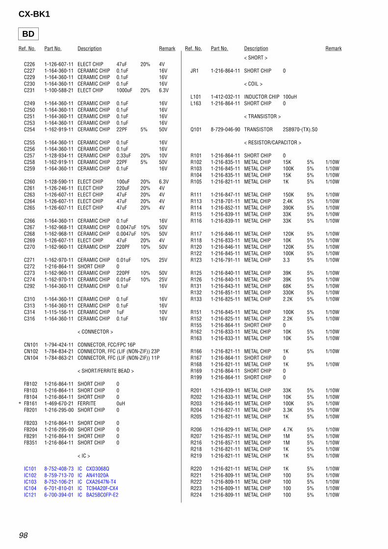
Ref. No. Part No. Description Remark Ref. No. Part No. Description Remark
98
CX-BK1
C226 1-126-607-11 ELECT CHIP 47uF 20% 4VC227 1-164-360-11 CERAMIC CHIP 0.1uF 16VC229 1-164-360-11 CERAMIC CHIP 0.1uF 16VC230 1-164-360-11 CERAMIC CHIP 0.1uF 16VC231 1-100-588-21 ELECT CHIP 1000uF 20% 6.3V
C249 1-164-360-11 CERAMIC CHIP 0.1uF 16VC250 1-164-360-11 CERAMIC CHIP 0.1uF 16VC251 1-164-360-11 CERAMIC CHIP 0.1uF 16VC253 1-164-360-11 CERAMIC CHIP 0.1uF 16VC254 1-162-919-11 CERAMIC CHIP 22PF 5% 50V
C255 1-164-360-11 CERAMIC CHIP 0.1uF 16VC256 1-164-360-11 CERAMIC CHIP 0.1uF 16VC257 1-128-934-11 CERAMIC CHIP 0.33uF 20% 10VC258 1-162-919-11 CERAMIC CHIP 22PF 5% 50VC259 1-164-360-11 CERAMIC CHIP 0.1uF 16V
C260 1-128-590-11 ELECT CHIP 100uF 20% 6.3VC261 1-126-246-11 ELECT CHIP 220uF 20% 4VC263 1-126-607-11 ELECT CHIP 47uF 20% 4VC264 1-126-607-11 ELECT CHIP 47uF 20% 4VC265 1-126-607-11 ELECT CHIP 47uF 20% 4V
C266 1-164-360-11 CERAMIC CHIP 0.1uF 16VC267 1-162-968-11 CERAMIC CHIP 0.0047uF 10% 50VC268 1-162-968-11 CERAMIC CHIP 0.0047uF 10% 50VC269 1-126-607-11 ELECT CHIP 47uF 20% 4VC270 1-162-960-11 CERAMIC CHIP 220PF 10% 50V
C271 1-162-970-11 CERAMIC CHIP 0.01uF 10% 25VC272 1-216-864-11 SHORT CHIP 0C273 1-162-960-11 CERAMIC CHIP 220PF 10% 50VC274 1-162-970-11 CERAMIC CHIP 0.01uF 10% 25VC292 1-164-360-11 CERAMIC CHIP 0.1uF 16V
C310 1-164-360-11 CERAMIC CHIP 0.1uF 16VC313 1-164-360-11 CERAMIC CHIP 0.1uF 16VC314 1-115-156-11 CERAMIC CHIP 1uF 10VC316 1-164-360-11 CERAMIC CHIP 0.1uF 16V
< CONNECTOR >
CN101 1-794-424-11 CONNECTOR, FCC/FPC 16PCN102 1-784-834-21 CONNECTOR, FFC (LIF (NON-ZIF)) 23PCN104 1-784-863-21 CONNECTOR, FFC (LIF (NON-ZIF)) 11P
< SHORT/FERRITE BEAD >
FB102 1-216-864-11 SHORT CHIP 0FB103 1-216-864-11 SHORT CHIP 0FB104 1-216-864-11 SHORT CHIP 0
* FB161 1-469-670-21 FERRITE 0uHFB201 1-216-295-00 SHORT CHIP 0
FB203 1-216-864-11 SHORT CHIP 0FB204 1-216-295-00 SHORT CHIP 0FB291 1-216-864-11 SHORT CHIP 0FB351 1-216-864-11 SHORT CHIP 0
< IC >
IC101 8-752-408-73 IC CXD3068QIC102 8-759-713-70 IC AN41020AIC103 8-752-106-21 IC CXA2647N-T4IC104 6-701-810-01 IC TC94A20F-CX4IC121 6-700-394-01 IC BA25BC0FP-E2
< SHORT >
JR1 1-216-864-11 SHORT CHIP 0
< COIL >
L101 1-412-032-11 INDUCTOR CHIP 100uHL163 1-216-864-11 SHORT CHIP 0
< TRANSISTOR >
Q101 8-729-046-90 TRANSISTOR 2SB970-(TX).S0
< RESISTOR/CAPACITOR >
R101 1-216-864-11 SHORT CHIP 0R102 1-216-835-11 METAL CHIP 15K 5% 1/10WR103 1-216-845-11 METAL CHIP 100K 5% 1/10WR104 1-216-835-11 METAL CHIP 15K 5% 1/10WR105 1-216-821-11 METAL CHIP 1K 5% 1/10W
R111 1-216-847-11 METAL CHIP 150K 5% 1/10WR113 1-218-701-11 METAL CHIP 2.4K 5% 1/10WR114 1-216-852-11 METAL CHIP 390K 5% 1/10WR115 1-216-839-11 METAL CHIP 33K 5% 1/10WR116 1-216-839-11 METAL CHIP 33K 5% 1/10W
R117 1-216-846-11 METAL CHIP 120K 5% 1/10WR118 1-216-833-11 METAL CHIP 10K 5% 1/10WR120 1-216-846-11 METAL CHIP 120K 5% 1/10WR122 1-216-845-11 METAL CHIP 100K 5% 1/10WR123 1-216-791-11 METAL CHIP 3.3 5% 1/10W
R125 1-216-840-11 METAL CHIP 39K 5% 1/10WR126 1-216-840-11 METAL CHIP 39K 5% 1/10WR131 1-216-843-11 METAL CHIP 68K 5% 1/10WR132 1-216-851-11 METAL CHIP 330K 5% 1/10WR133 1-216-825-11 METAL CHIP 2.2K 5% 1/10W
R151 1-216-845-11 METAL CHIP 100K 5% 1/10WR152 1-216-825-11 METAL CHIP 2.2K 5% 1/10WR155 1-216-864-11 SHORT CHIP 0R162 1-216-833-11 METAL CHIP 10K 5% 1/10WR163 1-216-833-11 METAL CHIP 10K 5% 1/10W
R166 1-216-821-11 METAL CHIP 1K 5% 1/10WR167 1-216-864-11 SHORT CHIP 0R168 1-216-821-11 METAL CHIP 1K 5% 1/10WR169 1-216-864-11 SHORT CHIP 0R199 1-216-864-11 SHORT CHIP 0
R201 1-216-839-11 METAL CHIP 33K 5% 1/10WR202 1-216-833-11 METAL CHIP 10K 5% 1/10WR203 1-216-845-11 METAL CHIP 100K 5% 1/10WR204 1-216-827-11 METAL CHIP 3.3K 5% 1/10WR205 1-216-821-11 METAL CHIP 1K 5% 1/10W
R206 1-216-829-11 METAL CHIP 4.7K 5% 1/10WR207 1-216-857-11 METAL CHIP 1M 5% 1/10WR216 1-216-857-11 METAL CHIP 1M 5% 1/10WR218 1-216-821-11 METAL CHIP 1K 5% 1/10WR219 1-216-821-11 METAL CHIP 1K 5% 1/10W
R220 1-216-821-11 METAL CHIP 1K 5% 1/10WR221 1-216-809-11 METAL CHIP 100 5% 1/10WR222 1-216-809-11 METAL CHIP 100 5% 1/10WR223 1-216-809-11 METAL CHIP 100 5% 1/10WR224 1-216-809-11 METAL CHIP 100 5% 1/10W
BD

Ref. No. Part No. Description Remark Ref. No. Part No. Description Remark
99
CX-BK1
R225 1-216-809-11 METAL CHIP 100 5% 1/10WR226 1-216-809-11 METAL CHIP 100 5% 1/10WR227 1-216-809-11 METAL CHIP 100 5% 1/10WR230 1-216-811-11 METAL CHIP 150 5% 1/10WR231 1-216-815-11 METAL CHIP 330 5% 1/10W
R232 1-216-815-11 METAL CHIP 330 5% 1/10WR233 1-216-815-11 METAL CHIP 330 5% 1/10WR249 1-216-818-11 METAL CHIP 560 5% 1/10WR250 1-216-813-11 METAL CHIP 220 5% 1/10WR251 1-216-813-11 METAL CHIP 220 5% 1/10W
R252 1-216-857-11 METAL CHIP 1M 5% 1/10WR253 1-216-821-11 METAL CHIP 1K 5% 1/10WR255 1-216-809-11 METAL CHIP 100 5% 1/10WR257 1-216-809-11 METAL CHIP 100 5% 1/10WR259 1-216-809-11 METAL CHIP 100 5% 1/10W
R260 1-216-821-11 METAL CHIP 1K 5% 1/10WR261 1-164-360-11 CERAMIC CHIP 0.1uF 16VR265 1-216-813-11 METAL CHIP 220 5% 1/10WR266 1-216-813-11 METAL CHIP 220 5% 1/10WR271 1-216-833-11 METAL CHIP 10K 5% 1/10W
R272 1-216-829-11 METAL CHIP 4.7K 5% 1/10WR275 1-216-833-11 METAL CHIP 10K 5% 1/10WR276 1-216-809-11 METAL CHIP 100 5% 1/10WR279 1-216-809-11 METAL CHIP 100 5% 1/10WR284 1-162-960-11 CERAMIC CHIP 220PF 10% 50V
R291 1-216-864-11 SHORT CHIP 0R303 1-216-864-11 SHORT CHIP 0R308 1-216-864-11 SHORT CHIP 0R309 1-216-864-11 SHORT CHIP 0R310 1-216-864-11 SHORT CHIP 0
R311 1-216-864-11 SHORT CHIP 0R313 1-216-864-11 SHORT CHIP 0R314 1-216-864-11 SHORT CHIP 0R316 1-216-864-11 SHORT CHIP 0R318 1-216-864-11 SHORT CHIP 0
R319 1-216-864-11 SHORT CHIP 0R321 1-216-864-11 SHORT CHIP 0R351 1-216-864-11 SHORT CHIP 0
< VARIABLE RESISTOR >
RV101 1-223-997-21 RES, CARBON ADJ VAR 47K
< VIBRATOR >
X201 1-767-408-21 VIBRATOR, CRYSTAL (16.9344MHz)**************************************************************
A-4731-113-A CONNECTOR BOARD, COMPLETE***************************
< CAPACITOR >
C711 1-126-795-11 ELECT 10uF 20% 50VC751 1-164-159-21 CERAMIC 0.1uF 50VC752 1-164-159-21 CERAMIC 0.1uF 50VC753 1-164-159-21 CERAMIC 0.1uF 50VC754 1-164-159-21 CERAMIC 0.1uF 50V
C755 1-164-159-21 CERAMIC 0.1uF 50VC756 1-164-159-21 CERAMIC 0.1uF 50VC758 1-164-159-21 CERAMIC 0.1uF 50V
C761 1-162-306-11 CERAMIC 0.01uF 30% 16VC762 1-164-159-21 CERAMIC 0.1uF 50V
C763 1-164-159-21 CERAMIC 0.1uF 50VC764 1-164-159-21 CERAMIC 0.1uF 50VC765 1-164-159-21 CERAMIC 0.1uF 50VC766 1-164-159-21 CERAMIC 0.1uF 50VC767 1-164-159-21 CERAMIC 0.1uF 50V
C768 1-164-159-21 CERAMIC 0.1uF 50VC769 1-164-159-21 CERAMIC 0.1uF 50VC771 1-162-306-11 CERAMIC 0.01uF 30% 16VC781 1-162-306-11 CERAMIC 0.01uF 30% 16V
< CONNECTOR >
CN701 1-779-564-21 CONNECTOR, FFC (LIF (NON-ZIF)) 27PCN702 1-785-329-11 PIN, CONNECTOR (LIGHT ANGLE) 3PCN703 1-785-328-11 PIN, CONNECTOR (LIGHT ANGRE) 2P
* CN710 1-506-486-11 PIN, CONNECTOR 7P
< DIODE >
D701 8-719-921-40 DIODE MTZJ-T-77-4.7BD711 8-719-109-89 DIODE MTZJ-T-77-5.6BD721 8-719-982-03 DIODE MTZJ-T-77-3.6A
< IC >
IC701 8-759-598-69 IC BA6956ANIC711 8-759-598-69 IC BA6956ANIC721 8-759-598-69 IC BA6956AN
< TRANSISTOR >
Q731 8-729-029-66 TRANSISTOR RT1N141S-TP
< RESISTOR >
R701 1-249-415-11 CARBON 680 5% 1/4WR702 1-247-807-31 CARBON 100 5% 1/4WR711 1-249-415-11 CARBON 680 5% 1/4WR712 1-247-807-31 CARBON 100 5% 1/4WR721 1-249-415-11 CARBON 680 5% 1/4W
R722 1-247-807-31 CARBON 100 5% 1/4WR731 1-247-806-11 CARBON 91 5% 1/4WR732 1-249-417-11 CARBON 1K 5% 1/4WR733 1-249-429-11 CARBON 10K 5% 1/4WR734 1-249-429-11 CARBON 10K 5% 1/4W
**************************************************************
A-4733-420-A DECK BOARD, COMPLETE (EXCEPT US)*********************
< CAPACITOR >
C303 1-164-647-11 CERAMIC CHIP 0.0012uF 10% 50VC304 1-164-647-11 CERAMIC CHIP 0.0012uF 10% 50VC307 1-104-665-11 ELECT 100uF 20% 10VC308 1-104-665-11 ELECT 100uF 20% 10VC309 1-162-923-11 CERAMIC CHIP 47PF 5% 50V
C310 1-162-923-11 CERAMIC CHIP 47PF 5% 50VC313 1-163-019-00 CERAMIC CHIP 0.0068uF 10% 50VC314 1-163-019-00 CERAMIC CHIP 0.0068uF 10% 50VC315 1-126-964-11 ELECT 220uF 20% 16VC317 1-126-956-91 ELECT 0.1uF 20% 50V
BD CONNECTOR DECK
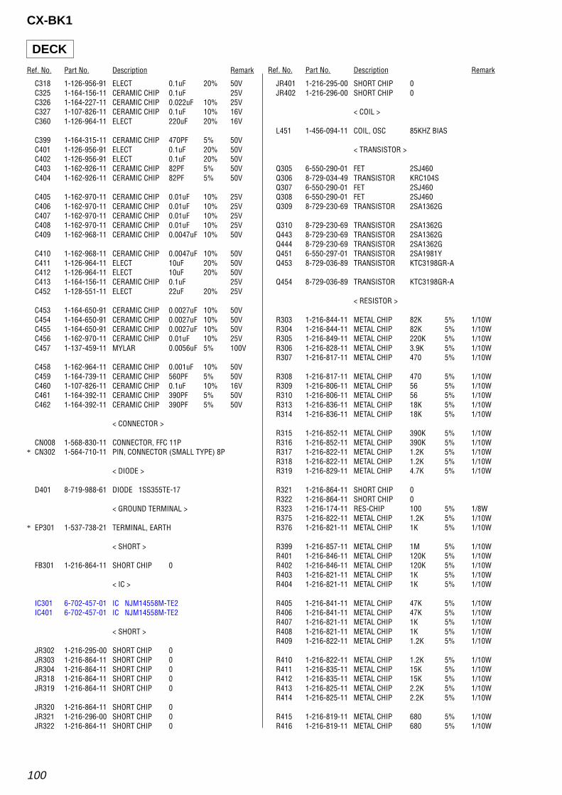
Ref. No. Part No. Description Remark Ref. No. Part No. Description Remark
100
CX-BK1
C318 1-126-956-91 ELECT 0.1uF 20% 50VC325 1-164-156-11 CERAMIC CHIP 0.1uF 25VC326 1-164-227-11 CERAMIC CHIP 0.022uF 10% 25VC327 1-107-826-11 CERAMIC CHIP 0.1uF 10% 16VC360 1-126-964-11 ELECT 220uF 20% 16V
C399 1-164-315-11 CERAMIC CHIP 470PF 5% 50VC401 1-126-956-91 ELECT 0.1uF 20% 50VC402 1-126-956-91 ELECT 0.1uF 20% 50VC403 1-162-926-11 CERAMIC CHIP 82PF 5% 50VC404 1-162-926-11 CERAMIC CHIP 82PF 5% 50V
C405 1-162-970-11 CERAMIC CHIP 0.01uF 10% 25VC406 1-162-970-11 CERAMIC CHIP 0.01uF 10% 25VC407 1-162-970-11 CERAMIC CHIP 0.01uF 10% 25VC408 1-162-970-11 CERAMIC CHIP 0.01uF 10% 25VC409 1-162-968-11 CERAMIC CHIP 0.0047uF 10% 50V
C410 1-162-968-11 CERAMIC CHIP 0.0047uF 10% 50VC411 1-126-964-11 ELECT 10uF 20% 50VC412 1-126-964-11 ELECT 10uF 20% 50VC413 1-164-156-11 CERAMIC CHIP 0.1uF 25VC452 1-128-551-11 ELECT 22uF 20% 25V
C453 1-164-650-91 CERAMIC CHIP 0.0027uF 10% 50VC454 1-164-650-91 CERAMIC CHIP 0.0027uF 10% 50VC455 1-164-650-91 CERAMIC CHIP 0.0027uF 10% 50VC456 1-162-970-11 CERAMIC CHIP 0.01uF 10% 25VC457 1-137-459-11 MYLAR 0.0056uF 5% 100V
C458 1-162-964-11 CERAMIC CHIP 0.001uF 10% 50VC459 1-164-739-11 CERAMIC CHIP 560PF 5% 50VC460 1-107-826-11 CERAMIC CHIP 0.1uF 10% 16VC461 1-164-392-11 CERAMIC CHIP 390PF 5% 50VC462 1-164-392-11 CERAMIC CHIP 390PF 5% 50V
< CONNECTOR >
CN008 1-568-830-11 CONNECTOR, FFC 11P* CN302 1-564-710-11 PIN, CONNECTOR (SMALL TYPE) 8P
< DIODE >
D401 8-719-988-61 DIODE 1SS355TE-17
< GROUND TERMINAL >
* EP301 1-537-738-21 TERMINAL, EARTH
< SHORT >
FB301 1-216-864-11 SHORT CHIP 0
< IC >
IC301 6-702-457-01 IC NJM14558M-TE2IC401 6-702-457-01 IC NJM14558M-TE2
< SHORT >
JR302 1-216-295-00 SHORT CHIP 0JR303 1-216-864-11 SHORT CHIP 0JR304 1-216-864-11 SHORT CHIP 0JR318 1-216-864-11 SHORT CHIP 0JR319 1-216-864-11 SHORT CHIP 0
JR320 1-216-864-11 SHORT CHIP 0JR321 1-216-296-00 SHORT CHIP 0JR322 1-216-864-11 SHORT CHIP 0
JR401 1-216-295-00 SHORT CHIP 0JR402 1-216-296-00 SHORT CHIP 0
< COIL >
L451 1-456-094-11 COIL, OSC 85KHZ BIAS
< TRANSISTOR >
Q305 6-550-290-01 FET 2SJ460Q306 8-729-034-49 TRANSISTOR KRC104SQ307 6-550-290-01 FET 2SJ460Q308 6-550-290-01 FET 2SJ460Q309 8-729-230-69 TRANSISTOR 2SA1362G
Q310 8-729-230-69 TRANSISTOR 2SA1362GQ443 8-729-230-69 TRANSISTOR 2SA1362GQ444 8-729-230-69 TRANSISTOR 2SA1362GQ451 6-550-297-01 TRANSISTOR 2SA1981YQ453 8-729-036-89 TRANSISTOR KTC3198GR-A
Q454 8-729-036-89 TRANSISTOR KTC3198GR-A
< RESISTOR >
R303 1-216-844-11 METAL CHIP 82K 5% 1/10WR304 1-216-844-11 METAL CHIP 82K 5% 1/10WR305 1-216-849-11 METAL CHIP 220K 5% 1/10WR306 1-216-828-11 METAL CHIP 3.9K 5% 1/10WR307 1-216-817-11 METAL CHIP 470 5% 1/10W
R308 1-216-817-11 METAL CHIP 470 5% 1/10WR309 1-216-806-11 METAL CHIP 56 5% 1/10WR310 1-216-806-11 METAL CHIP 56 5% 1/10WR313 1-216-836-11 METAL CHIP 18K 5% 1/10WR314 1-216-836-11 METAL CHIP 18K 5% 1/10W
R315 1-216-852-11 METAL CHIP 390K 5% 1/10WR316 1-216-852-11 METAL CHIP 390K 5% 1/10WR317 1-216-822-11 METAL CHIP 1.2K 5% 1/10WR318 1-216-822-11 METAL CHIP 1.2K 5% 1/10WR319 1-216-829-11 METAL CHIP 4.7K 5% 1/10W
R321 1-216-864-11 SHORT CHIP 0R322 1-216-864-11 SHORT CHIP 0R323 1-216-174-11 RES-CHIP 100 5% 1/8WR375 1-216-822-11 METAL CHIP 1.2K 5% 1/10WR376 1-216-821-11 METAL CHIP 1K 5% 1/10W
R399 1-216-857-11 METAL CHIP 1M 5% 1/10WR401 1-216-846-11 METAL CHIP 120K 5% 1/10WR402 1-216-846-11 METAL CHIP 120K 5% 1/10WR403 1-216-821-11 METAL CHIP 1K 5% 1/10WR404 1-216-821-11 METAL CHIP 1K 5% 1/10W
R405 1-216-841-11 METAL CHIP 47K 5% 1/10WR406 1-216-841-11 METAL CHIP 47K 5% 1/10WR407 1-216-821-11 METAL CHIP 1K 5% 1/10WR408 1-216-821-11 METAL CHIP 1K 5% 1/10WR409 1-216-822-11 METAL CHIP 1.2K 5% 1/10W
R410 1-216-822-11 METAL CHIP 1.2K 5% 1/10WR411 1-216-835-11 METAL CHIP 15K 5% 1/10WR412 1-216-835-11 METAL CHIP 15K 5% 1/10WR413 1-216-825-11 METAL CHIP 2.2K 5% 1/10WR414 1-216-825-11 METAL CHIP 2.2K 5% 1/10W
R415 1-216-819-11 METAL CHIP 680 5% 1/10WR416 1-216-819-11 METAL CHIP 680 5% 1/10W
DECK

Ref. No. Part No. Description Remark Ref. No. Part No. Description Remark
101
CX-BK1
R417 1-216-833-11 METAL CHIP 10K 5% 1/10WR418 1-216-833-11 METAL CHIP 10K 5% 1/10WR419 1-216-821-11 METAL CHIP 1K 5% 1/10W
R420 1-216-821-11 METAL CHIP 1K 5% 1/10WR421 1-216-837-11 METAL CHIP 22K 5% 1/10WR422 1-216-837-11 METAL CHIP 22K 5% 1/10WR423 1-216-836-11 METAL CHIP 18K 5% 1/10WR424 1-216-836-11 METAL CHIP 18K 5% 1/10W
R425 1-216-833-11 METAL CHIP 10K 5% 1/10WR453 1-216-663-91 METAL CHIP 3.3K 1/10WR454 1-216-148-00 RES-CHIP 8.2 5% 1/8WR455 1-216-836-11 METAL CHIP 18K 5% 1/10WR456 1-216-836-11 METAL CHIP 18K 5% 1/10W
R457 1-249-395-11 CARBON 15 5% 1/4WR458 1-216-845-11 METAL CHIP 100K 5% 1/10WR459 1-216-154-00 RES-CHIP 15 5% 1/8WR460 1-249-399-11 CARBON 33 5% 1/4WR465 1-216-845-11 METAL CHIP 100K 5% 1/10W
R466 1-216-845-11 METAL CHIP 100K 5% 1/10W
< VARIABLE RESISTOR >
SFR451 1-241-766-11 RES, ADJ, CARBON 33KSFR452 1-241-766-11 RES, ADJ, CARBON 33K
**************************************************************
1-688-414-11 HEADPHONE BOARD*****************
< CAPACITOR >
C550 1-115-467-11 CERAMIC CHIP 0.22 10% 10V
< CONNECTOR >
* CN530 1-564-520-11 PLUG, CONNECTOR 5P
< JACK >
J521 1-566-891-21 JACK (PHONES)
< SHORT >
JR501 1-216-296-00 SHORT CHIP 0
< RESISTOR >
R521 1-216-206-00 RES-CHIP 2.2K 5% 1/8WR522 1-216-206-00 RES-CHIP 2.2K 5% 1/8WR523 1-249-659-31 CARBON 270 5% 1/2WR524 1-249-659-31 CARBON 270 5% 1/2WR525 1-249-659-31 CARBON 270 5% 1/2W
R526 1-249-659-31 CARBON 270 5% 1/2W**************************************************************
1-688-413-11 JOG BOARD**********
< CAPACITOR >
C370 1-162-964-11 CERAMIC CHIP 0.001uF 10% 50VC371 1-162-927-11 CERAMIC CHIP 100PF 5% 50VC372 1-162-927-11 CERAMIC CHIP 100PF 5% 50V
< RESISTOR >
R376 1-216-833-11 METAL CHIP 10K 5% 1/10WR377 1-216-843-11 METAL CHIP 68K 5% 1/10WR378 1-216-835-11 METAL CHIP 15K 5% 1/10WR379 1-216-848-11 METAL CHIP 180K 5% 1/10WR380 1-216-833-11 METAL CHIP 10K 5% 1/10W
< SWITCH >
S304 1-478-133-11 ENCODER, ROTARY (MULTI JOG)**************************************************************
A-4733-395-A KEY LED RMC BOARD, COMPLETE****************************
< CAPACITOR >
C601 1-162-927-11 CERAMIC CHIP 100PF 5% 50VC602 1-162-927-11 CERAMIC CHIP 100PF 5% 50VC603 1-162-927-11 CERAMIC CHIP 100PF 5% 50VC604 1-162-927-11 CERAMIC CHIP 100PF 5% 50VC605 1-162-927-11 CERAMIC CHIP 100PF 5% 50V
C606 1-162-927-11 CERAMIC CHIP 100PF 5% 50VC607 1-124-234-00 ELECT 22uF 20% 16VC608 1-164-005-11 CERAMIC CHIP 0.47uF 25VC609 1-164-005-11 CERAMIC CHIP 0.47uF 25VC621 1-164-360-11 CERAMIC CHIP 0.1uF 16V
< CONNECTOR >
CN605 1-568-838-11 CONNECTOR, FFC 21P
< IC >
IC601 8-759-396-78 IC BU2092F-E2IC602 6-704-046-01 IC BU2099FVIC603 6-600-217-01 IC RPM7238-H4
< SHORT >
JR601 1-216-864-11 SHORT CHIP 0JR602 1-216-864-11 SHORT CHIP 0JR603 1-216-296-00 SHORT CHIP 0JR604 1-216-296-00 SHORT CHIP 0JR605 1-216-296-00 SHORT CHIP 0
JR606 1-216-296-00 SHORT CHIP 0JR607 1-216-296-00 SHORT CHIP 0JR608 1-216-296-00 SHORT CHIP 0JR609 1-216-296-00 SHORT CHIP 0JR610 1-216-296-00 SHORT CHIP 0
JR611 1-216-864-11 SHORT CHIP 0
< LED >
LED631 8-719-057-28 LED SML78420C-TP15 (DISC INDICATOR 1)LED632 8-719-057-28 LED SML78420C-TP15 (DISC INDICATOR 2)LED633 8-719-057-28 LED SML78420C-TP15 (DISC INDICATOR 3)LED634 8-719-057-28 LED SML78420C-TP15 (DISC INDICATOR 4)LED635 8-719-057-28 LED SML78420C-TP15 (DISC INDICATOR 5)
< TRANSISTOR >
Q601 6-550-336-01 TRANSISTOR FMA9AT148Q602 6-550-336-01 TRANSISTOR FMA9AT148Q603 6-550-336-01 TRANSISTOR FMA9AT148
DECK HEADPHONE JOG KEY LED RMC
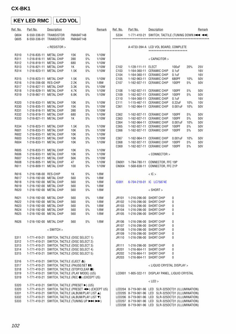
Ref. No. Part No. Description Remark Ref. No. Part No. Description Remark
102
CX-BK1
Q604 6-550-336-01 TRANSISTOR FMA9AT148Q605 6-550-336-01 TRANSISTOR FMA9AT148
< RESISTOR >
R310 1-216-835-11 METAL CHIP 15K 5% 1/10WR311 1-216-816-11 METAL CHIP 390 5% 1/10WR312 1-216-819-11 METAL CHIP 680 5% 1/10WR313 1-216-821-11 METAL CHIP 1K 5% 1/10WR314 1-216-823-11 METAL CHIP 1.5K 5% 1/10W
R315 1-216-823-11 METAL CHIP 1.5K 5% 1/10WR316 1-216-206-00 RES-CHIP 2.2K 5% 1/8WR317 1-216-827-11 METAL CHIP 3.3K 5% 1/10WR318 1-216-829-11 METAL CHIP 4.7K 5% 1/10WR319 1-218-867-11 METAL CHIP 6.8K 5% 1/10W
R320 1-216-833-11 METAL CHIP 10K 5% 1/10WR330 1-216-835-11 METAL CHIP 15K 5% 1/10WR331 1-216-816-11 METAL CHIP 390 5% 1/10WR332 1-216-819-11 METAL CHIP 680 5% 1/10WR333 1-216-821-11 METAL CHIP 1K 5% 1/10W
R334 1-216-823-11 METAL CHIP 1.5K 5% 1/10WR601 1-216-833-11 METAL CHIP 10K 5% 1/10WR602 1-216-833-11 METAL CHIP 10K 5% 1/10WR603 1-216-833-11 METAL CHIP 10K 5% 1/10WR604 1-216-833-11 METAL CHIP 10K 5% 1/10W
R605 1-216-833-11 METAL CHIP 10K 5% 1/10WR606 1-216-833-11 METAL CHIP 10K 5% 1/10WR607 1-216-842-11 METAL CHIP 56K 5% 1/10WR608 1-216-805-11 METAL CHIP 47 5% 1/10WR611 1-216-809-11 METAL CHIP 100 5% 1/10W
R616 1-216-198-00 RES-CHIP 1K 5% 1/8WR617 1-216-192-00 METAL CHIP 560 5% 1/8WR618 1-216-192-00 METAL CHIP 560 5% 1/8WR619 1-216-192-00 METAL CHIP 560 5% 1/8WR620 1-216-192-00 METAL CHIP 560 5% 1/8W
R621 1-216-192-00 METAL CHIP 560 5% 1/8WR622 1-216-192-00 METAL CHIP 560 5% 1/8WR623 1-216-192-00 METAL CHIP 560 5% 1/8WR624 1-216-192-00 METAL CHIP 560 5% 1/8WR625 1-216-192-00 METAL CHIP 560 5% 1/8W
R626 1-216-192-00 METAL CHIP 560 5% 1/8W
< SWITCH >
S311 1-771-410-21 SWITCH, TACTILE (DISC SELECT 1)S312 1-771-410-21 SWITCH, TACTILE (DISC SELECT 2)S313 1-771-410-21 SWITCH, TACTILE (DISC SELECT 3)S314 1-771-410-21 SWITCH, TACTILE (DISC SELECT 4)S315 1-771-410-21 SWITCH, TACTILE (DISC SELECT 5)
S316 1-771-410-21 SWITCH, TACTILE (EJECT Z)S317 1-771-410-21 SWITCH, TACTILE (PAUSE/SET X)S318 1-771-410-21 SWITCH, TACTILE (STOP/CLEAR x)S319 1-771-410-21 SWITCH, TACTILE (PLAY MODE) (US)S319 1-771-410-21 SWITCH, TACTILE (REC z) (EXCEPT US)
S320 1-771-410-21 SWITCH, TACTILE (PRESET B) (US)S320 1-771-410-21 SWITCH, TACTILE (PRESET Y) (EXCEPT US)S331 1-771-410-21 SWITCH, TACTILE (ALBUM/PLAY LIST v)S332 1-771-410-21 SWITCH, TACTILE (ALBUM/PLAY LIST V)S333 1-771-410-21 SWITCH, TACTILE (TUNING UP > M)
S334 1-771-410-21 SWITCH, TACTILE (TUNING DOWN . m)**************************************************************
A-4733-394-A LCD VOL BOARD, COMPLETE************************
< CAPACITOR >
C102 1-128-111-11 ELECT 100uF 20% 25VC103 1-164-360-11 CERAMIC CHIP 0.1uF 16VC104 1-164-360-11 CERAMIC CHIP 0.1uF 16VC105 1-162-963-11 CERAMIC CHIP 680PF 10% 50VC107 1-162-927-11 CERAMIC CHIP 100PF 5% 50V
C108 1-162-927-11 CERAMIC CHIP 100PF 5% 50VC109 1-162-927-11 CERAMIC CHIP 100PF 5% 50VC110 1-164-360-11 CERAMIC CHIP 0.1uF 16VC111 1-115-467-11 CERAMIC CHIP 0.22uF 10% 10VC361 1-162-964-11 CERAMIC CHIP 0.001uF 10% 50V
C362 1-162-927-11 CERAMIC CHIP 100PF 5% 50VC363 1-162-927-11 CERAMIC CHIP 100PF 5% 50VC364 1-162-964-11 CERAMIC CHIP 0.001uF 10% 50VC365 1-162-927-11 CERAMIC CHIP 100PF 5% 50VC366 1-162-927-11 CERAMIC CHIP 100PF 5% 50V
C367 1-162-964-11 CERAMIC CHIP 0.001uF 10% 50VC368 1-162-927-11 CERAMIC CHIP 100PF 5% 50VC369 1-162-927-11 CERAMIC CHIP 100PF 5% 50V
< CONNECTOR >
CN001 1-784-780-11 CONNECTOR, FFC 19PCN004 1-568-838-11 CONNECTOR, FFC 21P
< IC >
IC001 6-704-218-01 IC LC75874E
< SHORT >
JR101 1-216-296-00 SHORT CHIP 0JR102 1-216-296-00 SHORT CHIP 0JR103 1-216-296-00 SHORT CHIP 0JR104 1-216-296-00 SHORT CHIP 0JR105 1-216-296-00 SHORT CHIP 0
JR106 1-216-296-00 SHORT CHIP 0JR107 1-216-296-00 SHORT CHIP 0JR108 1-216-296-00 SHORT CHIP 0JR109 1-216-296-00 SHORT CHIP 0JR110 1-216-296-00 SHORT CHIP 0
JR111 1-216-296-00 SHORT CHIP 0JR201 1-216-864-11 SHORT CHIP 0JR202 1-216-864-11 SHORT CHIP 0JR203 1-216-864-11 SHORT CHIP 0
< LIQUID CRYSTAL DISPLAY >
LCD001 1-805-322-11 DISPLAY PANEL, LIQUID CRYSTAL
< LED >
LED204 8-719-061-96 LED SLR-325DCT31 (ILLUMINATION)LED205 8-719-061-96 LED SLR-325DCT31 (ILLUMINATION)LED206 8-719-061-96 LED SLR-325DCT31 (ILLUMINATION)LED207 8-719-061-96 LED SLR-325DCT31 (ILLUMINATION)LED208 8-719-061-96 LED SLR-325DCT31 (ILLUMINATION)
KEY LED RMC LCD VOL
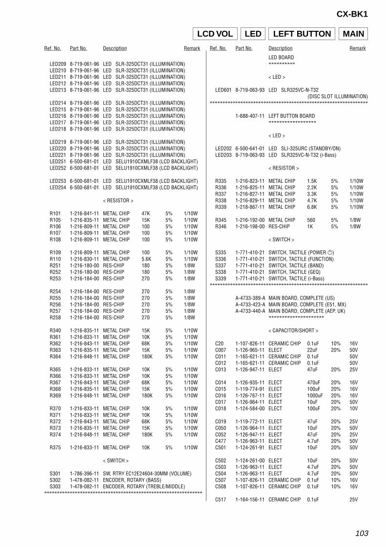
Ref. No. Part No. Description Remark Ref. No. Part No. Description Remark
103
CX-BK1
LED209 8-719-061-96 LED SLR-325DCT31 (ILLUMINATION)LED210 8-719-061-96 LED SLR-325DCT31 (ILLUMINATION)LED211 8-719-061-96 LED SLR-325DCT31 (ILLUMINATION)LED212 8-719-061-96 LED SLR-325DCT31 (ILLUMINATION)LED213 8-719-061-96 LED SLR-325DCT31 (ILLUMINATION)
LED214 8-719-061-96 LED SLR-325DCT31 (ILLUMINATION)LED215 8-719-061-96 LED SLR-325DCT31 (ILLUMINATION)LED216 8-719-061-96 LED SLR-325DCT31 (ILLUMINATION)LED217 8-719-061-96 LED SLR-325DCT31 (ILLUMINATION)LED218 8-719-061-96 LED SLR-325DCT31 (ILLUMINATION)
LED219 8-719-061-96 LED SLR-325DCT31 (ILLUMINATION)LED220 8-719-061-96 LED SLR-325DCT31 (ILLUMINATION)LED221 8-719-061-96 LED SLR-325DCT31 (ILLUMINATION)LED251 6-500-681-01 LED SELU1910CXMLF38 (LCD BACKLIGHT)LED252 6-500-681-01 LED SELU1910CXMLF38 (LCD BACKLIGHT)
LED253 6-500-681-01 LED SELU1910CXMLF38 (LCD BACKLIGHT)LED254 6-500-681-01 LED SELU1910CXMLF38 (LCD BACKLIGHT)
< RESISTOR >
R101 1-216-841-11 METAL CHIP 47K 5% 1/10WR105 1-216-835-11 METAL CHIP 15K 5% 1/10WR106 1-216-809-11 METAL CHIP 100 5% 1/10WR107 1-216-809-11 METAL CHIP 100 5% 1/10WR108 1-216-809-11 METAL CHIP 100 5% 1/10W
R109 1-216-809-11 METAL CHIP 100 5% 1/10WR110 1-216-830-11 METAL CHIP 5.6K 5% 1/10WR251 1-216-180-00 RES-CHIP 180 5% 1/8WR252 1-216-180-00 RES-CHIP 180 5% 1/8WR253 1-216-184-00 RES-CHIP 270 5% 1/8W
R254 1-216-184-00 RES-CHIP 270 5% 1/8WR255 1-216-184-00 RES-CHIP 270 5% 1/8WR256 1-216-184-00 RES-CHIP 270 5% 1/8WR257 1-216-184-00 RES-CHIP 270 5% 1/8WR258 1-216-184-00 RES-CHIP 270 5% 1/8W
R340 1-216-835-11 METAL CHIP 15K 5% 1/10WR361 1-216-833-11 METAL CHIP 10K 5% 1/10WR362 1-216-843-11 METAL CHIP 68K 5% 1/10WR363 1-216-835-11 METAL CHIP 15K 5% 1/10WR364 1-216-848-11 METAL CHIP 180K 5% 1/10W
R365 1-216-833-11 METAL CHIP 10K 5% 1/10WR366 1-216-833-11 METAL CHIP 10K 5% 1/10WR367 1-216-843-11 METAL CHIP 68K 5% 1/10WR368 1-216-835-11 METAL CHIP 15K 5% 1/10WR369 1-216-848-11 METAL CHIP 180K 5% 1/10W
R370 1-216-833-11 METAL CHIP 10K 5% 1/10WR371 1-216-833-11 METAL CHIP 10K 5% 1/10WR372 1-216-843-11 METAL CHIP 68K 5% 1/10WR373 1-216-835-11 METAL CHIP 15K 5% 1/10WR374 1-216-848-11 METAL CHIP 180K 5% 1/10W
R375 1-216-833-11 METAL CHIP 10K 5% 1/10W
< SWITCH >
S301 1-786-396-11 SW, RTRY EC12E24604-30MM (VOLUME)S302 1-478-082-11 ENCODER, ROTARY (BASS)S303 1-478-082-11 ENCODER, ROTARY (TREBLE/MIDDLE)
**************************************************************
LED BOARD**********
< LED >
LED601 8-719-063-93 LED SLR325VC-N-T32(DISC SLOT ILLUMINATION)
**************************************************************
1-688-407-11 LEFT BUTTON BOARD******************
< LED >
LED202 6-500-641-01 LED SLI-325URC (STANDBY/ON)LED203 8-719-063-93 LED SLR325VC-N-T32 (i-Bass)
< RESISTOR >
R335 1-216-823-11 METAL CHIP 1.5K 5% 1/10WR336 1-216-825-11 METAL CHIP 2.2K 5% 1/10WR337 1-216-827-11 METAL CHIP 3.3K 5% 1/10WR338 1-216-829-11 METAL CHIP 4.7K 5% 1/10WR339 1-218-867-11 METAL CHIP 6.8K 5% 1/10W
R345 1-216-192-00 METAL CHIP 560 5% 1/8WR346 1-216-198-00 RES-CHIP 1K 5% 1/8W
< SWITCH >
S335 1-771-410-21 SWITCH, TACTILE (POWER 1)S336 1-771-410-21 SWITCH, TACTILE (FUNCTION)S337 1-771-410-21 SWITCH, TACTILE (BAND)S338 1-771-410-21 SWITCH, TACTILE (GEQ)S339 1-771-410-21 SWITCH, TACTILE (i-Bass)
**************************************************************
A-4733-389-A MAIN BOARD, COMPLETE (US)A-4733-423-A MAIN BOARD, COMPLETE (E51, MX)A-4733-440-A MAIN BOARD, COMPLETE (AEP. UK)
*********************
< CAPACITOR/SHORT >
C20 1-107-826-11 CERAMIC CHIP 0.1uF 10% 16VC007 1-126-965-11 ELECT 22uF 20% 50VC011 1-165-621-11 CERAMIC CHIP 0.1uF 50VC012 1-165-621-11 CERAMIC CHIP 0.1uF 50VC013 1-126-947-11 ELECT 47uF 20% 25V
C014 1-126-935-11 ELECT 470uF 20% 16VC015 1-119-774-91 ELECT 100uF 20% 16VC016 1-126-767-11 ELECT 1000uF 20% 16VC017 1-126-964-11 ELECT 10uF 20% 50VC018 1-124-584-00 ELECT 100uF 20% 10V
C019 1-119-772-11 ELECT 47uF 20% 25VC050 1-126-964-11 ELECT 10uF 20% 50VC052 1-126-947-11 ELECT 47uF 20% 25VC477 1-126-963-11 ELECT 4.7uF 20% 50VC501 1-124-261-91 ELECT 10uF 20% 50V
C502 1-124-261-00 ELECT 10uF 20% 50VC503 1-126-963-11 ELECT 4.7uF 20% 50VC504 1-126-963-11 ELECT 4.7uF 20% 50VC507 1-107-826-11 CERAMIC CHIP 0.1uF 10% 16VC508 1-107-826-11 CERAMIC CHIP 0.1uF 10% 16V
C517 1-164-156-11 CERAMIC CHIP 0.1uF 25V
LCD VOL LED LEFT BUTTON MAIN
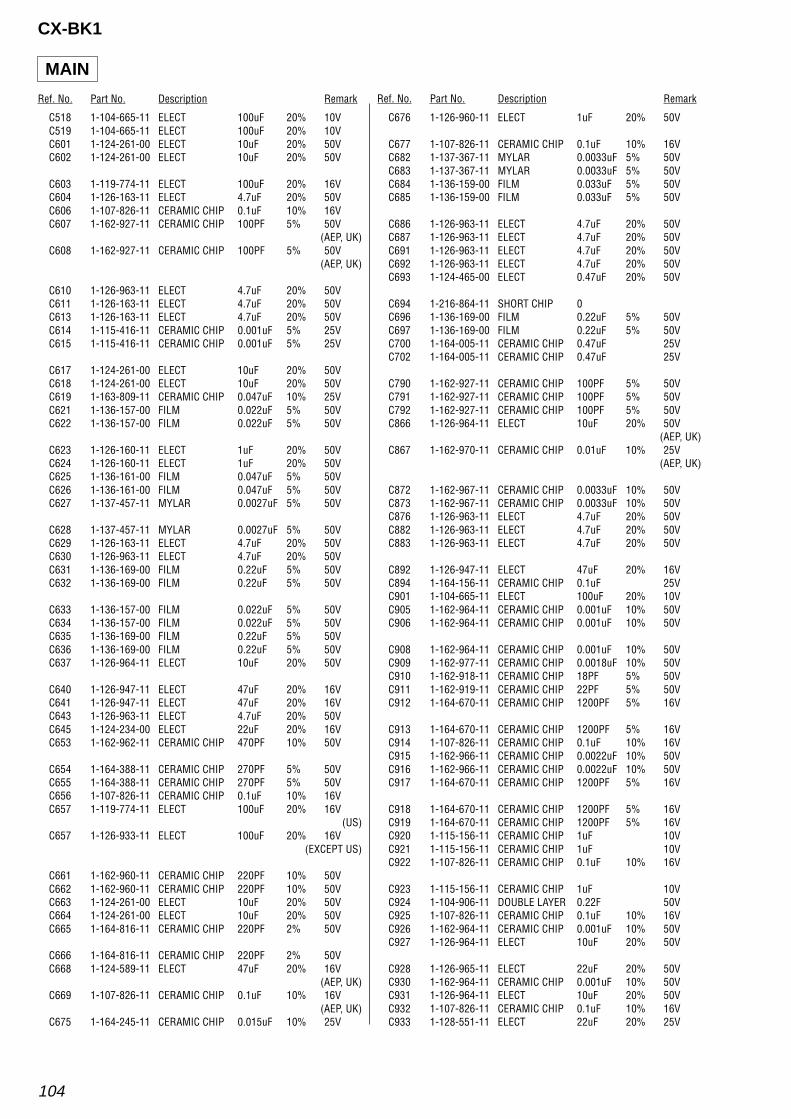
Ref. No. Part No. Description Remark Ref. No. Part No. Description Remark
104
CX-BK1
C518 1-104-665-11 ELECT 100uF 20% 10VC519 1-104-665-11 ELECT 100uF 20% 10VC601 1-124-261-00 ELECT 10uF 20% 50VC602 1-124-261-00 ELECT 10uF 20% 50V
C603 1-119-774-11 ELECT 100uF 20% 16VC604 1-126-163-11 ELECT 4.7uF 20% 50VC606 1-107-826-11 CERAMIC CHIP 0.1uF 10% 16VC607 1-162-927-11 CERAMIC CHIP 100PF 5% 50V
(AEP, UK)C608 1-162-927-11 CERAMIC CHIP 100PF 5% 50V
(AEP, UK)
C610 1-126-963-11 ELECT 4.7uF 20% 50VC611 1-126-163-11 ELECT 4.7uF 20% 50VC613 1-126-163-11 ELECT 4.7uF 20% 50VC614 1-115-416-11 CERAMIC CHIP 0.001uF 5% 25VC615 1-115-416-11 CERAMIC CHIP 0.001uF 5% 25V
C617 1-124-261-00 ELECT 10uF 20% 50VC618 1-124-261-00 ELECT 10uF 20% 50VC619 1-163-809-11 CERAMIC CHIP 0.047uF 10% 25VC621 1-136-157-00 FILM 0.022uF 5% 50VC622 1-136-157-00 FILM 0.022uF 5% 50V
C623 1-126-160-11 ELECT 1uF 20% 50VC624 1-126-160-11 ELECT 1uF 20% 50VC625 1-136-161-00 FILM 0.047uF 5% 50VC626 1-136-161-00 FILM 0.047uF 5% 50VC627 1-137-457-11 MYLAR 0.0027uF 5% 50V
C628 1-137-457-11 MYLAR 0.0027uF 5% 50VC629 1-126-163-11 ELECT 4.7uF 20% 50VC630 1-126-963-11 ELECT 4.7uF 20% 50VC631 1-136-169-00 FILM 0.22uF 5% 50VC632 1-136-169-00 FILM 0.22uF 5% 50V
C633 1-136-157-00 FILM 0.022uF 5% 50VC634 1-136-157-00 FILM 0.022uF 5% 50VC635 1-136-169-00 FILM 0.22uF 5% 50VC636 1-136-169-00 FILM 0.22uF 5% 50VC637 1-126-964-11 ELECT 10uF 20% 50V
C640 1-126-947-11 ELECT 47uF 20% 16VC641 1-126-947-11 ELECT 47uF 20% 16VC643 1-126-963-11 ELECT 4.7uF 20% 50VC645 1-124-234-00 ELECT 22uF 20% 16VC653 1-162-962-11 CERAMIC CHIP 470PF 10% 50V
C654 1-164-388-11 CERAMIC CHIP 270PF 5% 50VC655 1-164-388-11 CERAMIC CHIP 270PF 5% 50VC656 1-107-826-11 CERAMIC CHIP 0.1uF 10% 16VC657 1-119-774-11 ELECT 100uF 20% 16V
(US)C657 1-126-933-11 ELECT 100uF 20% 16V
(EXCEPT US)
C661 1-162-960-11 CERAMIC CHIP 220PF 10% 50VC662 1-162-960-11 CERAMIC CHIP 220PF 10% 50VC663 1-124-261-00 ELECT 10uF 20% 50VC664 1-124-261-00 ELECT 10uF 20% 50VC665 1-164-816-11 CERAMIC CHIP 220PF 2% 50V
C666 1-164-816-11 CERAMIC CHIP 220PF 2% 50VC668 1-124-589-11 ELECT 47uF 20% 16V
(AEP, UK)C669 1-107-826-11 CERAMIC CHIP 0.1uF 10% 16V
(AEP, UK)C675 1-164-245-11 CERAMIC CHIP 0.015uF 10% 25V
C676 1-126-960-11 ELECT 1uF 20% 50V
C677 1-107-826-11 CERAMIC CHIP 0.1uF 10% 16VC682 1-137-367-11 MYLAR 0.0033uF 5% 50VC683 1-137-367-11 MYLAR 0.0033uF 5% 50VC684 1-136-159-00 FILM 0.033uF 5% 50VC685 1-136-159-00 FILM 0.033uF 5% 50V
C686 1-126-963-11 ELECT 4.7uF 20% 50VC687 1-126-963-11 ELECT 4.7uF 20% 50VC691 1-126-963-11 ELECT 4.7uF 20% 50VC692 1-126-963-11 ELECT 4.7uF 20% 50VC693 1-124-465-00 ELECT 0.47uF 20% 50V
C694 1-216-864-11 SHORT CHIP 0C696 1-136-169-00 FILM 0.22uF 5% 50VC697 1-136-169-00 FILM 0.22uF 5% 50VC700 1-164-005-11 CERAMIC CHIP 0.47uF 25VC702 1-164-005-11 CERAMIC CHIP 0.47uF 25V
C790 1-162-927-11 CERAMIC CHIP 100PF 5% 50VC791 1-162-927-11 CERAMIC CHIP 100PF 5% 50VC792 1-162-927-11 CERAMIC CHIP 100PF 5% 50VC866 1-126-964-11 ELECT 10uF 20% 50V
(AEP, UK)C867 1-162-970-11 CERAMIC CHIP 0.01uF 10% 25V
(AEP, UK)
C872 1-162-967-11 CERAMIC CHIP 0.0033uF 10% 50VC873 1-162-967-11 CERAMIC CHIP 0.0033uF 10% 50VC876 1-126-963-11 ELECT 4.7uF 20% 50VC882 1-126-963-11 ELECT 4.7uF 20% 50VC883 1-126-963-11 ELECT 4.7uF 20% 50V
C892 1-126-947-11 ELECT 47uF 20% 16VC894 1-164-156-11 CERAMIC CHIP 0.1uF 25VC901 1-104-665-11 ELECT 100uF 20% 10VC905 1-162-964-11 CERAMIC CHIP 0.001uF 10% 50VC906 1-162-964-11 CERAMIC CHIP 0.001uF 10% 50V
C908 1-162-964-11 CERAMIC CHIP 0.001uF 10% 50VC909 1-162-977-11 CERAMIC CHIP 0.0018uF 10% 50VC910 1-162-918-11 CERAMIC CHIP 18PF 5% 50VC911 1-162-919-11 CERAMIC CHIP 22PF 5% 50VC912 1-164-670-11 CERAMIC CHIP 1200PF 5% 16V
C913 1-164-670-11 CERAMIC CHIP 1200PF 5% 16VC914 1-107-826-11 CERAMIC CHIP 0.1uF 10% 16VC915 1-162-966-11 CERAMIC CHIP 0.0022uF 10% 50VC916 1-162-966-11 CERAMIC CHIP 0.0022uF 10% 50VC917 1-164-670-11 CERAMIC CHIP 1200PF 5% 16V
C918 1-164-670-11 CERAMIC CHIP 1200PF 5% 16VC919 1-164-670-11 CERAMIC CHIP 1200PF 5% 16VC920 1-115-156-11 CERAMIC CHIP 1uF 10VC921 1-115-156-11 CERAMIC CHIP 1uF 10VC922 1-107-826-11 CERAMIC CHIP 0.1uF 10% 16V
C923 1-115-156-11 CERAMIC CHIP 1uF 10VC924 1-104-906-11 DOUBLE LAYER 0.22F 50VC925 1-107-826-11 CERAMIC CHIP 0.1uF 10% 16VC926 1-162-964-11 CERAMIC CHIP 0.001uF 10% 50VC927 1-126-964-11 ELECT 10uF 20% 50V
C928 1-126-965-11 ELECT 22uF 20% 50VC930 1-162-964-11 CERAMIC CHIP 0.001uF 10% 50VC931 1-126-964-11 ELECT 10uF 20% 50VC932 1-107-826-11 CERAMIC CHIP 0.1uF 10% 16VC933 1-128-551-11 ELECT 22uF 20% 25V
MAIN

Ref. No. Part No. Description Remark Ref. No. Part No. Description Remark
105
CX-BK1
C934 1-126-933-11 ELECT 100uF 20% 16VC935 1-164-227-11 CERAMIC CHIP 0.022uF 10% 25VC936 1-126-933-11 ELECT 100uF 20% 16VC938 1-126-960-11 ELECT 1uF 20% 50VC939 1-164-156-11 CERAMIC CHIP 0.1uF 25V
C940 1-126-767-11 ELECT 1000uF 20% 16VC943 1-162-964-11 CERAMIC CHIP 0.001uF 10% 50VC944 1-162-964-11 CERAMIC CHIP 0.001uF 10% 50VC945 1-107-826-11 CERAMIC CHIP 0.1uF 10% 16VC946 1-162-927-11 CERAMIC CHIP 100PF 5% 50V
C948 1-162-927-11 CERAMIC CHIP 100PF 5% 50VC949 1-162-927-11 CERAMIC CHIP 100PF 5% 50VC950 1-162-927-11 CERAMIC CHIP 100PF 5% 50VC951 1-162-927-11 CERAMIC CHIP 100PF 5% 50VC952 1-162-927-11 CERAMIC CHIP 100PF 5% 50V
C953 1-164-227-11 CERAMIC CHIP 0.022uF 10% 25VC954 1-164-173-11 CERAMIC CHIP 0.0039uF 10% 50VC955 1-162-927-11 CERAMIC CHIP 100PF 5% 50VC956 1-162-927-11 CERAMIC CHIP 100PF 5% 50VC957 1-162-927-11 CERAMIC CHIP 100PF 5% 50V
C958 1-162-964-11 CERAMIC CHIP 0.001uF 10% 50VC959 1-162-964-11 CERAMIC CHIP 0.001uF 10% 50VC960 1-162-964-11 CERAMIC CHIP 0.001uF 10% 50VC961 1-162-964-11 CERAMIC CHIP 0.001uF 10% 50VC962 1-162-964-11 CERAMIC CHIP 0.001uF 10% 50V
C963 1-162-964-11 CERAMIC CHIP 0.001uF 10% 50V
< CONNECTOR >
CN004 1-784-778-11 CONNECTOR, FFC 17PCN006 1-564-509-11 PLUG, CONNECTOR 6PCN007 1-564-507-11 PLUG, CONNECTOR 4PCN009 1-568-830-11 CONNECTOR, FFC 11P (EXCEPT US)CN502 1-784-733-11 CONNECTOR, FFC 11P
CN504 1-784-766-11 CONNECTOR, FFC 5P (E51, MX)CN507 1-779-279-11 CONNECTOR, FFC (LIF (NON-ZIF)) 11PCN508 1-784-776-11 CONNECTOR, FFC 15P (AEP. UK)CN509 1-568-830-11 CONNECTOR, FFC 11P (EXCEPT AEP, UK)CN901 1-779-295-11 CONNECTOR, FFC (LIF (NON-ZIF)) 27P
CN902 1-779-291-11 CONNECTOR, FFC (LIF (NON-ZIF)) 23PCN903 1-691-040-31 CONNECTOR, FFC 8P (EXCEPT US)CN905 1-784-780-11 CONNECTOR, FFC 19PCN999 1-568-826-11 CONNECTOR, FFC 7P
< DIODE >
D015 8-719-421-18 DIODE MA8033-L-TXD016 8-719-988-61 DIODE 1SS355TE-17D017 8-719-988-61 DIODE 1SS355TE-17D018 8-719-988-61 DIODE 1SS355TE-17D050 8-719-988-61 DIODE 1SS355TE-17
D501 8-719-083-58 DIODE UDZSTE-173.9BD611 8-719-988-61 DIODE 1SS355TE-17D612 8-719-988-61 DIODE 1SS355TE-17D613 8-719-988-61 DIODE 1SS355TE-17D902 8-719-988-61 DIODE 1SS355TE-17
D904 8-719-988-61 DIODE 1SS355TE-17D905 8-719-988-61 DIODE 1SS355TE-17D906 8-719-988-61 DIODE 1SS355TE-17D907 8-719-988-61 DIODE 1SS355TE-17 (EXCEPT US)
MAIN
D910 8-719-423-10 DIODE MA8100-M-TX
D911 8-719-988-61 DIODE 1SS355TE-17
< IC >
IC101 8-759-231-57 IC TA7810SIC501 8-759-525-25 IC BU4052BCF-E2IC601 6-703-650-11 IC M61529FP-D60GIC603 6-704-074-01 IC NJM2156M (TE2)IC604 6-600-234-01 IC GP1FA313TZ (DIGITAL OPTICAL OUT)
(AEP. UK)
IC701 6-704-046-01 IC BU2099FVIC703 6-704-046-01 IC BU2099FVIC901 6-803-325-01 IC uPD703260YGF-S04-JBT-AIC902 6-704-798-01 IC BD4923GIC904 8-759-533-04 IC M62703ML-E1
IC905 6-704-135-01 IC MM1614A
< JACK >
JK602 1-779-902-21 JACK, PIN 4P (AUX IN/OUT)JK603 1-774-227-11 JACK, PIN 1P (VIDEO OUT)
< SHORT >
JR001 1-216-296-00 SHORT CHIP 0JR002 1-216-296-00 SHORT CHIP 0JR501 1-216-864-11 SHORT CHIP 0JR502 1-216-296-00 SHORT CHIP 0JR503 1-216-864-11 SHORT CHIP 0
JR601 1-216-296-00 SHORT CHIP 0JR607 1-216-864-11 SHORT CHIP 0JR610 1-216-864-11 SHORT CHIP 0JR611 1-216-864-11 SHORT CHIP 0JR612 1-216-864-11 SHORT CHIP 0
JR613 1-216-864-11 SHORT CHIP 0JR614 1-216-864-11 SHORT CHIP 0JR615 1-216-864-11 SHORT CHIP 0JR616 1-216-864-11 SHORT CHIP 0JR617 1-216-864-11 SHORT CHIP 0
JR620 1-216-864-11 SHORT CHIP 0JR621 1-216-864-11 SHORT CHIP 0JR624 1-216-864-11 SHORT CHIP 0 (US, AEP, UK)JR701 1-216-296-00 SHORT CHIP 0JR702 1-216-864-11 SHORT CHIP 0
JR703 1-216-864-11 SHORT CHIP 0JR704 1-216-864-11 SHORT CHIP 0JR705 1-216-864-11 SHORT CHIP 0JR706 1-216-864-11 SHORT CHIP 0JR707 1-216-864-11 SHORT CHIP 0
JR708 1-216-864-11 SHORT CHIP 0JR709 1-216-864-11 SHORT CHIP 0JR801 1-216-296-00 SHORT CHIP 0JR802 1-216-864-11 SHORT CHIP 0JR901 1-216-864-11 SHORT CHIP 0
JR902 1-216-864-11 SHORT CHIP 0JR903 1-216-864-11 SHORT CHIP 0JR904 1-216-296-00 SHORT CHIP 0JR905 1-216-296-00 SHORT CHIP 0JR906 1-216-296-00 SHORT CHIP 0
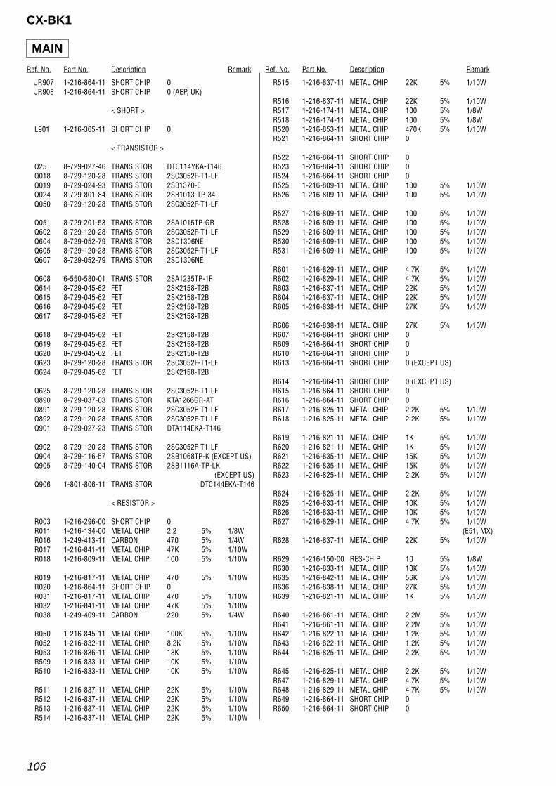
Ref. No. Part No. Description Remark Ref. No. Part No. Description Remark
106
CX-BK1
JR907 1-216-864-11 SHORT CHIP 0JR908 1-216-864-11 SHORT CHIP 0 (AEP, UK)
< SHORT >
L901 1-216-365-11 SHORT CHIP 0
< TRANSISTOR >
Q25 8-729-027-46 TRANSISTOR DTC114YKA-T146Q018 8-729-120-28 TRANSISTOR 2SC3052F-T1-LFQ019 8-729-024-93 TRANSISTOR 2SB1370-EQ024 8-729-801-84 TRANSISTOR 2SB1013-TP-34Q050 8-729-120-28 TRANSISTOR 2SC3052F-T1-LF
Q051 8-729-201-53 TRANSISTOR 2SA1015TP-GRQ602 8-729-120-28 TRANSISTOR 2SC3052F-T1-LFQ604 8-729-052-79 TRANSISTOR 2SD1306NEQ605 8-729-120-28 TRANSISTOR 2SC3052F-T1-LFQ607 8-729-052-79 TRANSISTOR 2SD1306NE
Q608 6-550-580-01 TRANSISTOR 2SA1235TP-1FQ614 8-729-045-62 FET 2SK2158-T2BQ615 8-729-045-62 FET 2SK2158-T2BQ616 8-729-045-62 FET 2SK2158-T2BQ617 8-729-045-62 FET 2SK2158-T2B
Q618 8-729-045-62 FET 2SK2158-T2BQ619 8-729-045-62 FET 2SK2158-T2BQ620 8-729-045-62 FET 2SK2158-T2BQ623 8-729-120-28 TRANSISTOR 2SC3052F-T1-LFQ624 8-729-045-62 FET 2SK2158-T2B
Q625 8-729-120-28 TRANSISTOR 2SC3052F-T1-LFQ890 8-729-037-03 TRANSISTOR KTA1266GR-ATQ891 8-729-120-28 TRANSISTOR 2SC3052F-T1-LFQ892 8-729-120-28 TRANSISTOR 2SC3052F-T1-LFQ901 8-729-027-23 TRANSISTOR DTA114EKA-T146
Q902 8-729-120-28 TRANSISTOR 2SC3052F-T1-LFQ904 8-729-116-57 TRANSISTOR 2SB1068TP-K (EXCEPT US)Q905 8-729-140-04 TRANSISTOR 2SB1116A-TP-LK
(EXCEPT US)Q906 1-801-806-11 TRANSISTOR DTC144EKA-T146
< RESISTOR >
R003 1-216-296-00 SHORT CHIP 0R011 1-216-134-00 METAL CHIP 2.2 5% 1/8WR016 1-249-413-11 CARBON 470 5% 1/4WR017 1-216-841-11 METAL CHIP 47K 5% 1/10WR018 1-216-809-11 METAL CHIP 100 5% 1/10W
R019 1-216-817-11 METAL CHIP 470 5% 1/10WR020 1-216-864-11 SHORT CHIP 0R031 1-216-817-11 METAL CHIP 470 5% 1/10WR032 1-216-841-11 METAL CHIP 47K 5% 1/10WR038 1-249-409-11 CARBON 220 5% 1/4W
R050 1-216-845-11 METAL CHIP 100K 5% 1/10WR052 1-216-832-11 METAL CHIP 8.2K 5% 1/10WR053 1-216-836-11 METAL CHIP 18K 5% 1/10WR509 1-216-833-11 METAL CHIP 10K 5% 1/10WR510 1-216-833-11 METAL CHIP 10K 5% 1/10W
R511 1-216-837-11 METAL CHIP 22K 5% 1/10WR512 1-216-837-11 METAL CHIP 22K 5% 1/10WR513 1-216-837-11 METAL CHIP 22K 5% 1/10WR514 1-216-837-11 METAL CHIP 22K 5% 1/10W
R515 1-216-837-11 METAL CHIP 22K 5% 1/10W
R516 1-216-837-11 METAL CHIP 22K 5% 1/10WR517 1-216-174-11 METAL CHIP 100 5% 1/8WR518 1-216-174-11 METAL CHIP 100 5% 1/8WR520 1-216-853-11 METAL CHIP 470K 5% 1/10WR521 1-216-864-11 SHORT CHIP 0
R522 1-216-864-11 SHORT CHIP 0R523 1-216-864-11 SHORT CHIP 0R524 1-216-864-11 SHORT CHIP 0R525 1-216-809-11 METAL CHIP 100 5% 1/10WR526 1-216-809-11 METAL CHIP 100 5% 1/10W
R527 1-216-809-11 METAL CHIP 100 5% 1/10WR528 1-216-809-11 METAL CHIP 100 5% 1/10WR529 1-216-809-11 METAL CHIP 100 5% 1/10WR530 1-216-809-11 METAL CHIP 100 5% 1/10WR531 1-216-809-11 METAL CHIP 100 5% 1/10W
R601 1-216-829-11 METAL CHIP 4.7K 5% 1/10WR602 1-216-829-11 METAL CHIP 4.7K 5% 1/10WR603 1-216-837-11 METAL CHIP 22K 5% 1/10WR604 1-216-837-11 METAL CHIP 22K 5% 1/10WR605 1-216-838-11 METAL CHIP 27K 5% 1/10W
R606 1-216-838-11 METAL CHIP 27K 5% 1/10WR607 1-216-864-11 SHORT CHIP 0R609 1-216-864-11 SHORT CHIP 0R610 1-216-864-11 SHORT CHIP 0R613 1-216-864-11 SHORT CHIP 0 (EXCEPT US)
R614 1-216-864-11 SHORT CHIP 0 (EXCEPT US)R615 1-216-864-11 SHORT CHIP 0R616 1-216-864-11 SHORT CHIP 0R617 1-216-825-11 METAL CHIP 2.2K 5% 1/10WR618 1-216-825-11 METAL CHIP 2.2K 5% 1/10W
R619 1-216-821-11 METAL CHIP 1K 5% 1/10WR620 1-216-821-11 METAL CHIP 1K 5% 1/10WR621 1-216-835-11 METAL CHIP 15K 5% 1/10WR622 1-216-835-11 METAL CHIP 15K 5% 1/10WR623 1-216-825-11 METAL CHIP 2.2K 5% 1/10W
R624 1-216-825-11 METAL CHIP 2.2K 5% 1/10WR625 1-216-833-11 METAL CHIP 10K 5% 1/10WR626 1-216-833-11 METAL CHIP 10K 5% 1/10WR627 1-216-829-11 METAL CHIP 4.7K 5% 1/10W
(E51, MX)R628 1-216-837-11 METAL CHIP 22K 5% 1/10W
R629 1-216-150-00 RES-CHIP 10 5% 1/8WR630 1-216-833-11 METAL CHIP 10K 5% 1/10WR635 1-216-842-11 METAL CHIP 56K 5% 1/10WR636 1-216-838-11 METAL CHIP 27K 5% 1/10WR639 1-216-821-11 METAL CHIP 1K 5% 1/10W
R640 1-216-861-11 METAL CHIP 2.2M 5% 1/10WR641 1-216-861-11 METAL CHIP 2.2M 5% 1/10WR642 1-216-822-11 METAL CHIP 1.2K 5% 1/10WR643 1-216-822-11 METAL CHIP 1.2K 5% 1/10WR644 1-216-825-11 METAL CHIP 2.2K 5% 1/10W
R645 1-216-825-11 METAL CHIP 2.2K 5% 1/10WR647 1-216-829-11 METAL CHIP 4.7K 5% 1/10WR648 1-216-829-11 METAL CHIP 4.7K 5% 1/10WR649 1-216-864-11 SHORT CHIP 0R650 1-216-864-11 SHORT CHIP 0
MAIN

Ref. No. Part No. Description Remark Ref. No. Part No. Description Remark
107
CX-BK1
R651 1-216-845-11 METAL CHIP 100K 5% 1/10WR652 1-216-845-11 METAL CHIP 100K 5% 1/10WR655 1-216-824-11 METAL CHIP 4.7K 5% 1/10WR656 1-216-830-11 METAL CHIP 5.6K 5% 1/10WR657 1-216-821-11 METAL CHIP 1K 5% 1/10W
R658 1-216-820-11 METAL CHIP 820 5% 1/10WR659 1-216-825-11 METAL CHIP 2.2K 5% 1/10WR660 1-216-825-11 METAL CHIP 3.3K 5% 1/10WR662 1-216-864-11 SHORT CHIP 0R663 1-216-833-11 METAL CHIP 10K 5% 1/10W
R664 1-216-836-11 METAL CHIP 18K 5% 1/10WR665 1-216-857-11 METAL CHIP 1M 5% 1/10WR666 1-216-814-11 METAL CHIP 270 5% 1/10WR667 1-216-833-11 METAL CHIP 10K 5% 1/10WR668 1-216-829-11 METAL CHIP 4.7K 5% 1/10W
R669 1-216-829-11 METAL CHIP 4.7K 5% 1/10WR670 1-216-809-11 METAL CHIP 100 5% 1/10WR671 1-216-809-11 METAL CHIP 100 5% 1/10WR672 1-216-829-11 METAL CHIP 4.7K 5% 1/10WR674 1-216-845-11 METAL CHIP 100K 5% 1/10W
R675 1-216-825-11 METAL CHIP 2.2K 5% 1/10R676 1-216-825-11 METAL CHIP 2.2K 5% 1/10R677 1-216-837-11 METAL CHIP 22K 5% 1/10WR678 1-216-849-11 METAL CHIP 220K 5% 1/10WR679 1-216-845-11 METAL CHIP 100K 5% 1/10W
R680 1-216-849-11 METAL CHIP 220K 5% 1/10WR681 1-216-849-11 METAL CHIP 220K 5% 1/10WR682 1-216-841-11 METAL CHIP 47K 5% 1/10WR683 1-216-844-11 METAL CHIP 82K 5% 1/10WR684 1-216-833-11 METAL CHIP 10K 5% 1/10W
R685 1-216-841-11 METAL CHIP 47K 5% 1/10WR686 1-216-832-11 METAL CHIP 8.2K 5% 1/10WR687 1-216-823-11 METAL CHIP 1.5K 5% 1/10WR688 1-216-823-11 METAL CHIP 1.5K 5% 1/10WR689 1-216-214-00 RES-CHIP 4.7K 5% 1/8W
R692 1-216-809-11 METAL CHIP 100 5% 1/10WR693 1-216-809-11 METAL CHIP 100 5% 1/10WR694 1-216-826-11 METAL CHIP 2.7K 5% 1/10WR695 1-216-826-11 METAL CHIP 2.7K 5% 1/10WR696 1-216-845-11 METAL CHIP 100K 5% 1/10W
R697 1-216-845-11 METAL CHIP 100K 5% 1/10WR698 1-216-830-11 METAL CHIP 5.6K 5% 1/10WR699 1-216-830-11 METAL CHIP 5.6K 5% 1/10WR701 1-216-849-11 METAL CHIP 220K 5% 1/10WR702 1-216-841-11 METAL CHIP 47K 5% 1/10W
R703 1-216-821-11 METAL CHIP 1K 5% 1/10WR704 1-216-821-11 METAL CHIP 1K 5% 1/10WR707 1-216-833-11 METAL CHIP 10K 5% 1/10WR708 1-216-833-11 METAL CHIP 10K 5% 1/10WR709 1-216-833-11 METAL CHIP 10K 5% 1/10W
R710 1-216-833-11 METAL CHIP 10K 5% 1/10WR711 1-216-833-11 METAL CHIP 10K 5% 1/10WR712 1-216-821-11 METAL CHIP 1K 5% 1/10WR713 1-216-821-11 METAL CHIP 1K 5% 1/10WR714 1-216-833-11 METAL CHIP 10K 5% 1/10W
R715 1-216-833-11 METAL CHIP 10K 5% 1/10WR716 1-216-833-11 METAL CHIP 10K 5% 1/10WR717 1-216-833-11 METAL CHIP 10K 5% 1/10W
R718 1-216-833-11 METAL CHIP 10K 5% 1/10WR719 1-216-833-11 METAL CHIP 10K 5% 1/10W
R721 1-216-833-11 METAL CHIP 10K 5% 1/10WR722 1-216-833-11 METAL CHIP 10K 5% 1/10WR723 1-216-821-11 METAL CHIP 1K 5% 1/10WR724 1-216-821-11 METAL CHIP 1K 5% 1/10WR725 1-216-821-11 METAL CHIP 1K 5% 1/10W
R726 1-216-821-11 METAL CHIP 1K 5% 1/10WR727 1-216-833-11 METAL CHIP 10K 5% 1/10WR728 1-216-833-11 METAL CHIP 10K 5% 1/10WR729 1-216-833-11 METAL CHIP 10K 5% 1/10WR730 1-216-821-11 METAL CHIP 1K 5% 1/10W
R731 1-216-825-11 METAL CHIP 2.2K 5% 1/10WR732 1-216-825-11 METAL CHIP 2.2K 5% 1/10WR733 1-216-821-11 METAL CHIP 1K 5% 1/10WR734 1-216-821-11 METAL CHIP 1K 5% 1/10WR737 1-216-825-11 METAL CHIP 2.2K 5% 1/10W
R738 1-216-821-11 METAL CHIP 1K 5% 1/10WR739 1-216-821-11 METAL CHIP 1K 5% 1/10WR740 1-216-821-11 METAL CHIP 1K 5% 1/10WR741 1-216-821-11 METAL CHIP 1K 5% 1/10WR744 1-216-821-11 METAL CHIP 1K 5% 1/10W
R745 1-216-821-11 METAL CHIP 1K 5% 1/10WR746 1-216-821-11 METAL CHIP 1K 5% 1/10WR747 1-216-821-11 METAL CHIP 1K 5% 1/10WR748 1-216-821-11 METAL CHIP 1K 5% 1/10WR749 1-216-821-11 METAL CHIP 1K 5% 1/10W
R750 1-216-821-11 METAL CHIP 1K 5% 1/10WR751 1-216-821-11 METAL CHIP 1K 5% 1/10WR752 1-216-825-11 METAL CHIP 2.2K 5% 1/10WR753 1-216-821-11 METAL CHIP 1K 5% 1/10WR754 1-216-821-11 METAL CHIP 1K 5% 1/10W
R755 1-216-829-11 METAL CHIP 4.7K 5% 1/10WR756 1-216-829-11 METAL CHIP 4.7K 5% 1/10WR759 1-216-829-11 METAL CHIP 4.7K 5% 1/10WR760 1-216-826-11 METAL CHIP 2.7K 5% 1/10WR761 1-216-833-11 METAL CHIP 10K 5% 1/10W
R762 1-216-826-11 METAL CHIP 2.7K 5% 1/10WR763 1-216-841-11 METAL CHIP 47K 5% 1/10W
(EXCEPT US)R764 1-216-826-11 METAL CHIP 2.7K 5% 1/10WR765 1-216-830-11 METAL CHIP 5.6K 5% 1/10WR766 1-216-826-11 METAL CHIP 2.7K 5% 1/10W
R767 1-216-830-11 METAL CHIP 5.6K 5% 1/10WR768 1-216-833-11 METAL CHIP 10K 5% 1/10WR769 1-216-830-11 METAL CHIP 5.6K 5% 1/10WR770 1-216-864-11 SHORT CHIP 0R771 1-216-864-11 SHORT CHIP 0
R772 1-216-864-11 SHORT CHIP 0R773 1-216-864-11 SHORT CHIP 0R774 1-216-864-11 SHORT CHIP 0R778 1-216-864-11 SHORT CHIP 0R779 1-216-864-11 SHORT CHIP 0
R780 1-216-864-11 SHORT CHIP 0R781 1-216-864-11 SHORT CHIP 0R782 1-216-841-11 METAL CHIP 47K 5% 1/10WR783 1-216-841-11 METAL CHIP 47K 5% 1/10WR784 1-216-841-11 METAL CHIP 47K 5% 1/10W
MAIN
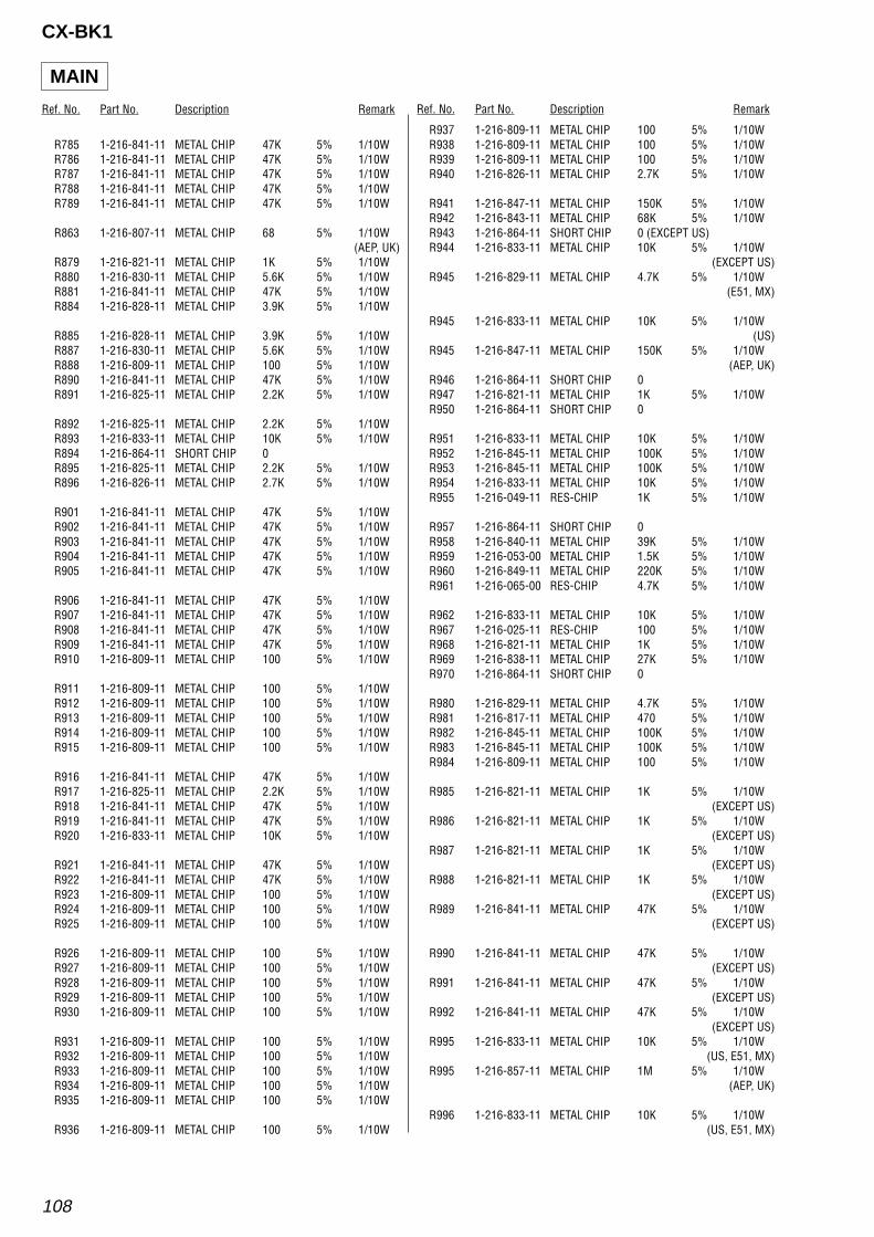
Ref. No. Part No. Description Remark Ref. No. Part No. Description Remark
108
CX-BK1
R785 1-216-841-11 METAL CHIP 47K 5% 1/10WR786 1-216-841-11 METAL CHIP 47K 5% 1/10WR787 1-216-841-11 METAL CHIP 47K 5% 1/10WR788 1-216-841-11 METAL CHIP 47K 5% 1/10WR789 1-216-841-11 METAL CHIP 47K 5% 1/10W
R863 1-216-807-11 METAL CHIP 68 5% 1/10W(AEP, UK)
R879 1-216-821-11 METAL CHIP 1K 5% 1/10WR880 1-216-830-11 METAL CHIP 5.6K 5% 1/10WR881 1-216-841-11 METAL CHIP 47K 5% 1/10WR884 1-216-828-11 METAL CHIP 3.9K 5% 1/10W
R885 1-216-828-11 METAL CHIP 3.9K 5% 1/10WR887 1-216-830-11 METAL CHIP 5.6K 5% 1/10WR888 1-216-809-11 METAL CHIP 100 5% 1/10WR890 1-216-841-11 METAL CHIP 47K 5% 1/10WR891 1-216-825-11 METAL CHIP 2.2K 5% 1/10W
R892 1-216-825-11 METAL CHIP 2.2K 5% 1/10WR893 1-216-833-11 METAL CHIP 10K 5% 1/10WR894 1-216-864-11 SHORT CHIP 0R895 1-216-825-11 METAL CHIP 2.2K 5% 1/10WR896 1-216-826-11 METAL CHIP 2.7K 5% 1/10W
R901 1-216-841-11 METAL CHIP 47K 5% 1/10WR902 1-216-841-11 METAL CHIP 47K 5% 1/10WR903 1-216-841-11 METAL CHIP 47K 5% 1/10WR904 1-216-841-11 METAL CHIP 47K 5% 1/10WR905 1-216-841-11 METAL CHIP 47K 5% 1/10W
R906 1-216-841-11 METAL CHIP 47K 5% 1/10WR907 1-216-841-11 METAL CHIP 47K 5% 1/10WR908 1-216-841-11 METAL CHIP 47K 5% 1/10WR909 1-216-841-11 METAL CHIP 47K 5% 1/10WR910 1-216-809-11 METAL CHIP 100 5% 1/10W
R911 1-216-809-11 METAL CHIP 100 5% 1/10WR912 1-216-809-11 METAL CHIP 100 5% 1/10WR913 1-216-809-11 METAL CHIP 100 5% 1/10WR914 1-216-809-11 METAL CHIP 100 5% 1/10WR915 1-216-809-11 METAL CHIP 100 5% 1/10W
R916 1-216-841-11 METAL CHIP 47K 5% 1/10WR917 1-216-825-11 METAL CHIP 2.2K 5% 1/10WR918 1-216-841-11 METAL CHIP 47K 5% 1/10WR919 1-216-841-11 METAL CHIP 47K 5% 1/10WR920 1-216-833-11 METAL CHIP 10K 5% 1/10W
R921 1-216-841-11 METAL CHIP 47K 5% 1/10WR922 1-216-841-11 METAL CHIP 47K 5% 1/10WR923 1-216-809-11 METAL CHIP 100 5% 1/10WR924 1-216-809-11 METAL CHIP 100 5% 1/10WR925 1-216-809-11 METAL CHIP 100 5% 1/10W
R926 1-216-809-11 METAL CHIP 100 5% 1/10WR927 1-216-809-11 METAL CHIP 100 5% 1/10WR928 1-216-809-11 METAL CHIP 100 5% 1/10WR929 1-216-809-11 METAL CHIP 100 5% 1/10WR930 1-216-809-11 METAL CHIP 100 5% 1/10W
R931 1-216-809-11 METAL CHIP 100 5% 1/10WR932 1-216-809-11 METAL CHIP 100 5% 1/10WR933 1-216-809-11 METAL CHIP 100 5% 1/10WR934 1-216-809-11 METAL CHIP 100 5% 1/10WR935 1-216-809-11 METAL CHIP 100 5% 1/10W
R936 1-216-809-11 METAL CHIP 100 5% 1/10W
R937 1-216-809-11 METAL CHIP 100 5% 1/10WR938 1-216-809-11 METAL CHIP 100 5% 1/10WR939 1-216-809-11 METAL CHIP 100 5% 1/10WR940 1-216-826-11 METAL CHIP 2.7K 5% 1/10W
R941 1-216-847-11 METAL CHIP 150K 5% 1/10WR942 1-216-843-11 METAL CHIP 68K 5% 1/10WR943 1-216-864-11 SHORT CHIP 0 (EXCEPT US)R944 1-216-833-11 METAL CHIP 10K 5% 1/10W
(EXCEPT US)R945 1-216-829-11 METAL CHIP 4.7K 5% 1/10W
(E51, MX)
R945 1-216-833-11 METAL CHIP 10K 5% 1/10W(US)
R945 1-216-847-11 METAL CHIP 150K 5% 1/10W(AEP, UK)
R946 1-216-864-11 SHORT CHIP 0R947 1-216-821-11 METAL CHIP 1K 5% 1/10WR950 1-216-864-11 SHORT CHIP 0
R951 1-216-833-11 METAL CHIP 10K 5% 1/10WR952 1-216-845-11 METAL CHIP 100K 5% 1/10WR953 1-216-845-11 METAL CHIP 100K 5% 1/10WR954 1-216-833-11 METAL CHIP 10K 5% 1/10WR955 1-216-049-11 RES-CHIP 1K 5% 1/10W
R957 1-216-864-11 SHORT CHIP 0R958 1-216-840-11 METAL CHIP 39K 5% 1/10WR959 1-216-053-00 METAL CHIP 1.5K 5% 1/10WR960 1-216-849-11 METAL CHIP 220K 5% 1/10WR961 1-216-065-00 RES-CHIP 4.7K 5% 1/10W
R962 1-216-833-11 METAL CHIP 10K 5% 1/10WR967 1-216-025-11 RES-CHIP 100 5% 1/10WR968 1-216-821-11 METAL CHIP 1K 5% 1/10WR969 1-216-838-11 METAL CHIP 27K 5% 1/10WR970 1-216-864-11 SHORT CHIP 0
R980 1-216-829-11 METAL CHIP 4.7K 5% 1/10WR981 1-216-817-11 METAL CHIP 470 5% 1/10WR982 1-216-845-11 METAL CHIP 100K 5% 1/10WR983 1-216-845-11 METAL CHIP 100K 5% 1/10WR984 1-216-809-11 METAL CHIP 100 5% 1/10W
R985 1-216-821-11 METAL CHIP 1K 5% 1/10W(EXCEPT US)
R986 1-216-821-11 METAL CHIP 1K 5% 1/10W(EXCEPT US)
R987 1-216-821-11 METAL CHIP 1K 5% 1/10W(EXCEPT US)
R988 1-216-821-11 METAL CHIP 1K 5% 1/10W(EXCEPT US)
R989 1-216-841-11 METAL CHIP 47K 5% 1/10W(EXCEPT US)
R990 1-216-841-11 METAL CHIP 47K 5% 1/10W(EXCEPT US)
R991 1-216-841-11 METAL CHIP 47K 5% 1/10W(EXCEPT US)
R992 1-216-841-11 METAL CHIP 47K 5% 1/10W(EXCEPT US)
R995 1-216-833-11 METAL CHIP 10K 5% 1/10W(US, E51, MX)
R995 1-216-857-11 METAL CHIP 1M 5% 1/10W(AEP, UK)
R996 1-216-833-11 METAL CHIP 10K 5% 1/10W(US, E51, MX)
MAIN

Ref. No. Part No. Description Remark Ref. No. Part No. Description Remark
109
CX-BK1
MAIN MIC MODE MOTOR PT RIGHT BUTTON (1)
R996 1-216-864-11 SHORT CHIP 0 (AEP, UK)R997 1-216-833-11 METAL CHIP 10K 5% 1/10W
(US, E51, MX)R997 1-216-864-11 SHORT CHIP 0 (AEP, UK)R998 1-220-397-11 METAL CHIP 4.7M 5% 1/10W
R999 1-216-851-11 METAL CHIP 330K 5% 1/10W
< VIBRATOR >
X901 1-760-252-12 VIBRATOR, CRYSTAL (32.768kHz)X902 1-795-058-21 VIBRATOR, CERAMIC (5MHz)
**************************************************************
A-4733-419-A MIC BOARD, COMPLETE (E51, MX)********************
< CAPACITOR >
C203 1-162-968-11 CERAMIC CHIP 0.0047uF 10% 50VC204 1-126-957-11 ELECT 0.22uF 20% 50VC205 1-126-964-11 ELECT 10uF 20% 50VC206 1-126-934-11 ELECT 220uF 20% 10VC207 1-162-928-11 CERAMIC CHIP 120PF 5% 50V
C208 1-126-960-11 ELECT 1uF 20% 50VC209 1-126-964-11 ELECT 10uF 20% 50VC210 1-126-965-11 ELECT 22uF 20% 50VC211 1-164-473-11 CERAMIC CHIP 820PF 5% 50VC212 1-126-959-11 ELECT 0.47uF 20% 50V
C213 1-126-961-11 ELECT 2.2uF 20% 50VC216 1-126-959-11 ELECT 0.47uF 20% 50VC219 1-115-467-11 CERAMIC CHIP 0.22uF 10% 10V
< CONNECTOR >
CN205 1-784-766-11 CONNECTOR, FFC 5P
< DIODE >
D201 8-719-988-61 DIODE 1SS355TE-17D202 8-719-988-61 DIODE 1SS355TE-17
< FERRITE BEAD >
* FB201 1-543-959-22 FERRITE 0uH
< IC >
IC201 8-759-710-97 IC NJM4565M (TE2)
< JACK >
J201 1-816-860-11 JACK, 6.3 BLK MONO W/SW V MSC (MIC)
< SHORT >
JR204 1-216-864-11 SHORT CHIP 0
< TRANSISTOR >
Q201 8-729-045-62 FET 2SK2158-T2B
< RESISTOR >
R201 1-216-833-11 METAL CHIP 10K 5% 1/10WR202 1-216-829-11 METAL CHIP 4.7K 5% 1/10WR203 1-216-849-11 METAL CHIP 220K 5% 1/10W
R204 1-216-809-11 METAL CHIP 100 5% 1/10WR205 1-216-825-11 METAL CHIP 2.2K 5% 1/10W
R206 1-216-850-11 METAL CHIP 270K 5% 1/10WR207 1-216-821-11 METAL CHIP 1K 5% 1/10WR208 1-216-174-00 RES-CHIP 100 5% 1/8WR209 1-216-817-11 METAL CHIP 470 5% 1/10WR210 1-216-825-11 METAL CHIP 2.2K 5% 1/10W
R211 1-216-825-11 METAL CHIP 2.2K 5% 1/10WR212 1-216-825-11 METAL CHIP 2.2K 5% 1/10WR213 1-216-839-11 METAL CHIP 33K 5% 1/10WR214 1-216-797-11 METAL CHIP 10 5% 1/10WR215 1-216-817-11 METAL CHIP 470 5% 1/10W
R216 1-216-821-11 METAL CHIP 1K 5% 1/10WR232 1-216-833-11 METAL CHIP 10K 5% 1/10W
< VARIABLE RESISTOR >
VR201 1-227-502-11 RES, VAR, CARBON 10K (MIC MIXING)**************************************************************
1-686-724-12 MODE MOTOR BOARD******************
**************************************************************
1-688-417-11 PT BOARD (US, AEP, UK)1-688-421-11 PT BOARD (E51, MX)
*********
< CAPACITOR >
C009 1-164-005-11 CERAMIC CHIP 0.47uF 25V(E51, MX)
C025 1-164-005-11 CERAMIC CHIP 0.47uF 25V(US, AEP, UK)
< CONNECTOR >
* CN001 1-564-915-11 PIN, CONNECTOR (3.96mm PITCH) 7P (US)* CN007 1-564-687-11 PIN, CONNECTOR (3.96mm PITCH) 3P (E51)* CN008 1-564-687-11 PIN, CONNECTOR (3.96mm PITCH) 3P (E51)* CN010 1-564-321-21 PIN, CONNECTOR (3.96mm PITCH) 2P
(EXCEPT E51)* CN011 1-564-242-00 PIN, CONNECTOR (3.96mm PITCH) 5P
(AEP, UK)
* CN015 1-564-915-11 PIN, CONNECTOR (3.96mm PITCH) 7P(E51, MX)
**************************************************************
1-688-408-11 RIGHT BUTTON (1) BOARD**********************
< RESISTOR >
R341 1-216-816-11 METAL CHIP 390 5% 1/10WR342 1-216-819-11 METAL CHIP 680 5% 1/10WR343 1-216-821-11 METAL CHIP 1K 5% 1/10WR344 1-216-823-11 METAL CHIP 1.5K 5% 1/10W
< SWITCH >
S341 1-771-410-21 SWITCH, TACTILE (TITLE)S342 1-771-410-21 SWITCH, TACTILE (DISPLAY)S343 1-771-410-21 SWITCH, TACTILE (MODE)
**************************************************************

Ref. No. Part No. Description Remark Ref. No. Part No. Description Remark
110
CX-BK1
1-688-409-11 RIGHT BUTTON (2) BOARD**********************
< SWITCH >
S344 1-771-410-21 SWITCH, TACTILE (ENTER)**************************************************************
1-686-726-12 ROLLER MOTOR BOARD********************
**************************************************************
1-686-723-12 SENSOR BOARD*************
< IC >
IC751 8-749-017-45 SENSOR, PHONT RPR-220C1N(DISC INSERT DETECT SENSOR)
**************************************************************
1-688-419-11 SPEAKER BOARD***************
< CAPACITOR >
C524 1-165-621-11 CERAMIC CHIP 0.1uF 50VC525 1-165-621-11 CERAMIC CHIP 0.1uF 50VC526 1-165-621-11 CERAMIC CHIP 0.1uF 50VC527 1-165-621-11 CERAMIC CHIP 0.1uF 50VC532 1-162-966-11 CERAMIC CHIP 0.0022uF 10% 50V
C533 1-162-966-11 CERAMIC CHIP 0.0022uF 10% 50VC534 1-165-621-11 CERAMIC CHIP 0.1uF 50VC535 1-165-621-11 CERAMIC CHIP 0.1uF 50V
< CONNECTOR >
* CN503 1-564-241-11 PIN, CONNECTOR (3.96mm PITCH) 4P
< JACK >
JK502 1-694-635-12 TERMINAL BOARD (4P) (5 SPEAKER)
< COIL >
L501 1-420-872-52 COIL, AIR-COREL502 1-420-872-52 COIL, AIR-CORE
< RESISTOR >
R570 1-249-625-31 CARBON 10 5% 1/2WR571 1-249-625-31 CARBON 10 5% 1/2WR572 1-249-393-11 CARBON 10 5% 1/4WR573 1-249-393-11 CARBON 10 5% 1/4W
**************************************************************
1-686-725-12 STOCKER MOTOR BOARD*********************
**************************************************************
1-686-727-12 SW (1) BOARD************
< SWITCH >
S711 1-786-382-11 SWITCH, PUSH (1 KEY)(DISC INSERT (8/12cm))
**************************************************************
1-686-728-12 SW (2) BOARD************
< SWITCH >
S713 1-786-382-11 SWITCH, PUSH (1 KEY) (DISC IN (8/12cm))S714 1-786-382-11 SWITCH, PUSH (1 KEY) (DISC IN (8cm))
**************************************************************
1-686-729-12 SW (3) BOARD************
< SWITCH >
S715 1-786-382-11 SWITCH, PUSH (1 KEY) (DISC OUT)**************************************************************
1-686-730-12 SW (4) BOARD************
< SWITCH >
S716 1-786-382-11 SWITCH, PUSH (1 KEY) (STOCKER IN/OUT)S717 1-786-382-11 SWITCH, PUSH (1 KEY) (DISC POSITION)S718 1-786-382-11 SWITCH, PUSH (1 KEY) (STOCKING)
**************************************************************
A-4733-399-A USB AUX BOARD, COMPLETE************************
< CAPACITOR >
C700 1-162-919-11 CERAMIC CHIP 22PF 5% 50VC701 1-162-919-11 CERAMIC CHIP 22PF 5% 50VC702 1-162-964-11 CERAMIC CHIP 0.001uF 10% 50VC703 1-162-964-11 CERAMIC CHIP 0.001uF 10% 50VC704 1-162-960-11 CERAMIC CHIP 220PF 10% 50V
C705 1-162-960-11 CERAMIC CHIP 220PF 10% 50VC706 1-162-970-11 CERAMIC CHIP 0.01uF 10% 25VC708 1-117-863-11 CERAMIC CHIP 0.47uF 10% 6.3VC709 1-164-156-11 CERAMIC CHIP 0.1uF 25VC710 1-164-156-11 CERAMIC CHIP 0.1uF 25V
C711 1-162-919-11 CERAMIC CHIP 22PF 5% 50VC712 1-125-891-11 CERAMIC CHIP 0.47uF 10% 10VC713 1-126-964-11 ELECT 10uF 20% 50VC714 1-162-919-11 CERAMIC CHIP 22PF 5% 50VC715 1-104-665-11 ELECT 100uF 20% 10V
C716 1-126-964-11 ELECT 10uF 20% 50VC717 1-104-663-11 ELECT 33uF 20% 25VC718 1-164-360-11 CERAMIC CHIP 0.1uF 16VC719 1-164-156-11 CERAMIC CHIP 0.1uF 25VC720 1-164-156-11 CERAMIC CHIP 0.1uF 25V
C721 1-164-156-11 CERAMIC CHIP 0.1uF 25VC722 1-164-156-11 CERAMIC CHIP 0.1uF 25VC724 1-162-927-11 CERAMIC CHIP 100PF 5% 50VC725 1-162-927-11 CERAMIC CHIP 100PF 5% 50V
RIGHT BUTTON (2) ROLLER MOTOR SENSOR
SPEAKER STOCKER SW (1) SW (2) SW (3) SW (4) USB AUX
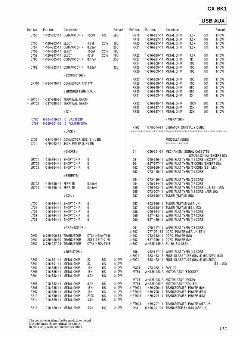
Ref. No. Part No. Description Remark Ref. No. Part No. Description Remark
111
CX-BK1
C755 1-162-927-11 CERAMIC CHIP 100PF 5% 50V
C756 1-126-963-11 ELECT 4.7uF 20% 50VC757 1-164-222-11 CERAMIC CHIP 0.22uF 25VC758 1-104-665-11 ELECT 100uF 20% 10VC759 1-126-947-11 ELECT 47uF 20% 10VC760 1-164-005-11 CERAMIC CHIP 0.47uF 25V
C762 1-164-222-11 CERAMIC CHIP 0.22uF 25V
< CONNECTOR >
CN701 1-784-778-11 CONNECTOR, FFC 17P
< GROUND TERMINAL >
* EP701 1-537-738-21 TERMINAL, EARTH* EP702 1-537-738-21 TERMINAL, EARTH
< IC >
IC700 6-704-219-01 IC UAC3553BIC701 8-759-701-56 IC NJM78M05FA
< JACK >
* J700 1-784-010-11 CONNECTOR, USB (B) (USB)J701 1-779-583-11 JACK, PIN 3P (LINE IN)
< SHORT >
JR701 1-216-864-11 SHORT CHIP 0JR702 1-216-864-11 SHORT CHIP 0JR703 1-216-864-11 SHORT CHIP 0
< FERRITE>
JN702 1-410-396-41 FERRITE 0.45uHJN704 1-410-396-41 FERRITE 0.45uH
< COIL >
L700 1-216-864-11 SHORT CHIP 0L701 1-216-864-11 SHORT CHIP 0L702 1-216-864-11 SHORT CHIP 0L703 1-216-864-11 SHORT CHIP 0L705 1-216-864-11 SHORT CHIP 0
< TRANSISTOR >
Q700 8-729-900-53 TRANSISTOR DTC114EKA-T146Q701 8-729-106-60 TRANSISTOR 2SB1132-T101-RQ702 8-729-027-23 TRANSISTOR DTA114EKA-T146
< RESISTOR >
R700 1-216-801-11 METAL CHIP 22 5% 1/10WR701 1-216-801-11 METAL CHIP 22 5% 1/10WR702 1-216-835-11 METAL CHIP 15K 5% 1/10WR703 1-216-835-11 METAL CHIP 15K 5% 1/10WR704 1-216-832-11 METAL CHIP 8.2K 5% 1/10W
R705 1-216-832-11 METAL CHIP 8.2K 5% 1/10WR706 1-216-835-11 METAL CHIP 15K 5% 1/10WR707 1-216-835-11 METAL CHIP 15K 5% 1/10WR710 1-216-849-11 METAL CHIP 220K 5% 1/10WR711 1-216-829-11 METAL CHIP 4.7K 5% 1/10W
R712 1-216-829-11 METAL CHIP 4.7K 5% 1/10W
The components identified by mark 0 or dottedline with mark 0 are critical for safety.Replace only with part number specified.
USB AUX
R716 1-216-827-11 METAL CHIP 3.3K 5% 1/10WR718 1-216-827-11 METAL CHIP 3.3K 5% 1/10WR720 1-216-827-11 METAL CHIP 3.3K 5% 1/10WR721 1-216-827-11 METAL CHIP 3.3K 5% 1/10W
R722 1-216-829-11 METAL CHIP 4.7K 5% 1/10WR723 1-216-821-11 METAL CHIP 1K 5% 1/10WR724 1-216-809-11 METAL CHIP 100 5% 1/10WR725 1-216-809-11 METAL CHIP 100 5% 1/10WR726 1-216-809-11 METAL CHIP 100 5% 1/10W
R727 1-216-809-11 METAL CHIP 100 5% 1/10WR728 1-216-809-11 METAL CHIP 100 5% 1/10WR729 1-216-819-11 METAL CHIP 680 5% 1/10WR730 1-216-819-11 METAL CHIP 680 5% 1/10WR731 1-216-803-11 METAL CHIP 33 5% 1/10W
R732 1-216-845-11 METAL CHIP 100K 5% 1/10WR735 1-216-837-11 METAL CHIP 22K 5% 1/10WR736 1-216-837-11 METAL CHIP 22K 5% 1/10W
< VIBRATOR >
X700 1-578-774-81 VIBRATOR, CRYSTAL (12MHz)************************************************************
MISCELLANEOUS**************
51 1-796-351-61 MECHANISM, SIGNAL CASSETTE(CMAL1Z241A) (EXCEPT US)
59 1-765-326-11 WIRE (FLAT TYPE) (11 CORE) (EXCEPT US)60 1-827-677-11 WIRE (FLAT TYPE) (8 CORE) (EXCEPT US)102 1-769-869-11 WIRE (FLAT TYPE) (5 CORE) (E51, MX)153 1-773-115-11 WIRE (FLAT TYPE) (19 CORE)
154 1-773-156-11 WIRE (FLAT TYPE) (21 CORE)254 1-765-334-11 WIRE (FLAT TYPE) (17 CORE)255 1-769-943-11 WIRE (FLAT TYPE) (11 CORE) (US, E51, MX)255 1-773-007-11 WIRE (FLAT TYPE) (15 CORE) (AEP, UK)257 1-693-625-11 TUNER (FM/AM) (US)
257 1-693-626-11 TUNER (FM/AM) (AEP, UK)257 1-693-628-11 TUNER (FM/AM) (E51, MX)258 1-769-944-11 WIRE (FLAT TYPE) (11 CORE)259 1-827-488-11 WIRE (FLAT TYPE) (27 CORE)260 1-827-489-11 WIRE (FLAT TYPE) (11 CORE)
261 1-775-217-11 WIRE (FLAT TYPE) (23 CORE)0303 1-777-071-83 CORD, POWER (AEP, UK, E51)0303 1-783-532-11 CORD, POWER (US)0303 1-827-226-11 CORD, POWER (MX)0807 A-4735-189-A BU-30 (61) ASSY
808 1-782-817-11 WIRE (FLAT TYPE) (16 CORE)0F001 1-533-453-12 FUSE, GLASS TUBE (DIA. 5) (5A/125V) (US)0F001 1-533-472-11 FUSE, GLASS TUBE (DIA. 5) (5A/250V)
(E51, MX)M301 1-763-072-11 FAN, DCM761 A-4735-953-A MOTOR ASSY (STOCKER)
M771 A-4735-953-A MOTOR ASSY (MODE)M781 A-4735-953-A MOTOR ASSY (ROLLER)
0PT001 1-439-796-11 TRANSFORMER, POWER (MX)0PT002 1-439-795-11 TRANSFORMER, POWER (E51)0PT003 1-439-794-11 TRANSFORMER, POWER (US)
0PT003 1-439-797-11 TRANSFORMER, POWER (AEP, UK)Q531 6-550-291-01 TRANSISTOR FN1016 (AEP, UK)
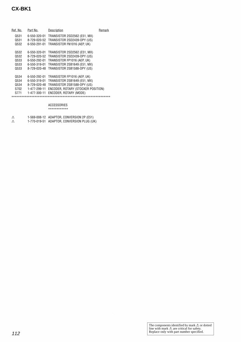
Ref. No. Part No. Description Remark Ref. No. Part No. Description Remark
112
CX-BK1
Q531 6-550-320-01 TRANSISTOR 2SD2562 (E51, MX)Q531 8-729-020-52 TRANSISTOR 2SD2439-OPY (US)Q532 6-550-291-01 TRANSISTOR FN1016 (AEP, UK)
Q532 6-550-320-01 TRANSISTOR 2SD2562 (E51, MX)Q532 8-729-020-52 TRANSISTOR 2SD2439-OPY (US)Q533 6-550-292-01 TRANSISTOR FP1016 (AEP, UK)Q533 6-550-319-01 TRANSISTOR 2SB1649 (E51, MX)Q533 8-729-020-48 TRANSISTOR 2SB1588-OPY (US)
Q534 6-550-292-01 TRANSISTOR FP1016 (AEP, UK)Q534 6-550-319-01 TRANSISTOR 2SB1649 (E51, MX)Q534 8-729-020-48 TRANSISTOR 2SB1588-OPY (US)S702 1-477-299-11 ENCODER, ROTARY (STOCKER POSITION)S771 1-477-300-11 ENCODER, ROTARY (MODE)
************************************************************
ACCESSORIES************
0 1-569-008-12 ADAPTOR, CONVERSION 2P (E51)0 1-770-019-51 ADAPTOR, CONVERSION PLUG (UK)
The components identified by mark 0 or dottedline with mark 0 are critical for safety.Replace only with part number specified.
113
CX-BK1
MEMO

CX-BK1
REVISION HISTORY
Clicking the version allows you to jump to the revised page.Also, clicking the version at the upper right on the revised page allows you to jump to the next revisedpage.
Ver. Date Description of Revision
1.0 2003.06 New
Related Documents