Curriculum Vitae Dr.Davinder Kaur Walia Date of birth: December 9, 1966 Present Designation: Professor Address for Correspondence: Department of Physics & Centre for Nanotechnology Indian Institute of Technology Roorkee, Roorkee Roorkee-247667, Uttarakhand , India Telephone: +91 1332 285407(O), +91 1332285474(R), +91 9760031912 E-Mail: [email protected] [email protected] Education :ED DEGREE INSTITUTION DIVISION YEAR Ph.D. Physics National Physical Laboratory, Delhi & Delhi Univ. - 1993 (High-T c Superconducting Thin Films & Josephson Junctions) Qualified NET “ CSIR-UGC” JRF National Eligibility Test - 1988 M.Sc. Physics University of Delhi First 1988 (Specialization: Electronics) B.Sc. (Hons.)Physics University of Delhi First 1986 Teaching Experience: 25 Years Research Experience: 28 Years Professor Indian Institute of Technology Roorkee, India April 2014- Present Associate Professor Indian Institute of Technology Roorkee, India Dec 2009 -April2014 Assistant Professor Indian Institute of Technology Roorkee, India Dec 2001 - Dec 2009 Lecturer Guru Nanak Dev University, Amritsar, India Oct 1991 - Dec 2001 Research Fellow National Physical Laboratory, Delhi Sept 1988- June 1993 Visiting Scientist Atomic Institute Vienna, Austria May 1997 - June 1997 Gestafesson Fellow Royal Institute of Science & Technology July 1997 - Aug 1998 Stockholm, Sweden Guest Scientist Oak Ridge National lab, USA April 1998 - May1998 Post doc Fellow Imperial College, London, U.K. March1999 - Oct 1999 Visiting Scientist T.I.F.R, Mumbai, India May 2004 - July 2004 EDUCATIONAL QUALIFICATIONS PROFESSIONAL & ACADEMIC EXPERIENCE

Welcome message from author
This document is posted to help you gain knowledge. Please leave a comment to let me know what you think about it! Share it to your friends and learn new things together.
Transcript

Curriculum Vitae
Dr.Davinder Kaur Walia
Date of birth: December 9, 1966
Present Designation: Professor
Address for Correspondence: Department of Physics & Centre for Nanotechnology
Indian Institute of Technology Roorkee, Roorkee
Roorkee-247667, Uttarakhand , India
Telephone: +91 1332 285407(O), +91 1332285474(R), +91 9760031912
E-Mail: [email protected]
Education:ED
DEGREE INSTITUTION DIVISION YEAR
Ph.D. Physics National Physical Laboratory, Delhi & Delhi Univ. - 1993
(High-Tc Superconducting Thin Films & Josephson Junctions)
Qualified NET “ CSIR-UGC” JRF National Eligibility Test - 1988
M.Sc. Physics University of Delhi First 1988
(Specialization: Electronics)
B.Sc. (Hons.)Physics University of Delhi First 1986
Teaching Experience: 25 Years Research Experience: 28 Years
Professor Indian Institute of Technology Roorkee, India April 2014- Present
Associate Professor Indian Institute of Technology Roorkee, India Dec 2009 -April2014
Assistant Professor Indian Institute of Technology Roorkee, India Dec 2001 - Dec 2009
Lecturer Guru Nanak Dev University, Amritsar, India Oct 1991 - Dec 2001
Research Fellow National Physical Laboratory, Delhi Sept 1988- June 1993
Visiting Scientist Atomic Institute Vienna, Austria May 1997 - June 1997
Gestafesson Fellow Royal Institute of Science & Technology July 1997 - Aug 1998
Stockholm, Sweden
Guest Scientist Oak Ridge National lab, USA April 1998 - May1998
Post doc Fellow Imperial College, London, U.K. March1999 - Oct 1999
Visiting Scientist T.I.F.R, Mumbai, India May 2004 - July 2004
EDUCATIONAL QUALIFICATIONS
PROFESSIONAL & ACADEMIC EXPERIENCE

Shastri Indo-Canadian Fellowship Award (2017).
V.N.M.M Research Award for Innovative work in Nanostructured Thin FilmDevices (2012).
Star Performer Award for Best Teaching & Research Performance at I.I.T Roorkee(2004).
Major Research Project of Rs. 4.84 Crore from Ministry of Information Technology, India to Work on
Nanotechnology Initiative Program of National Importance (2008-2013).
Best Poster Paper Award In International Conference IUMRS-ICAM (2007).
Scroll of Merit from Indian Cryogenics for Best Research Work on High-Tc SQUIDs (1990).
Gestafesson Fellowship At Royal Institute of Science & Technology, Stockholm Sweden (1997).
Commonwealth Fellowship at U.K.(1995).
Functional Nanomaterials for MEMS & Optoelectronic Applications
Multiferroic Heterostructures & Multilayers for RT Electronics
Superhard Nanocomposite Coatings for Industrial Applications
Resistive Memory Switching & High Temperature Electronics
Low Dimensional Semiconductor Nanostructures
Superconducting Microwave Resonators & Josephson Junction Devices
Principle Investigator
Development of Multiferroic heterostructures integrated on Silicon for MERAM and magnetic sensor
applications
Department of Science & Technology (DST), Budget: Rs. 50.87 Lacs, 2017- 2020
Principle Investigator
Synthesis & Characterization Of Functional Nanostructures For MEMS And Optoelectronics
Ministry of Information Technology (MIT) Budget: Rs. 4.84 Crore, 2008-2013
Principle Investigator
Fabrication of Nanostructured Multiferroic Thin Films and Multilavers for RT Etectronic
Defence Research & Development Organisation, Budget: Rs.47.99 Lacs, 2012- 2015
Principle Investigator
Fabrication of SMA/PZT Heterostructures for Smart Systems.
Defence Research & Development Organisation, Budget: Rs. 9.89 Lacs, 2008- 2011
Principle Investigator
Functional Nanocomposites: Synthesis, Characterization & Applications
Department of Science & Technology, Budget: Rs. 94.15 Lacs, 2006- 2009
Principle Investigator
Fabrication of Superhard Nanocomposite Coatings of Transition Metal Nitrides
Defence Research & Development Organisation, Budget: Rs. 9.97 Lacs, 2004- 2007
Principle Investigator
Development of High-Tc Superconducting Coated Conductors
Council of Scientific & Industrial Research, Budget: Rs. 12.26 Lacs , 2003-2006
Co-Principle Investigator
To Study Mechanical Properties Of Nanophase Materials
AWARDS
MAJOR RESEARCH PROJECTS Total Grant : Rs. 749.00 Lacs
AREAS OF RESEARCH: NANOSTRUCTURED THIN FILMS & DEVICES
Department of Science & Technology, Budget : Rs. 24.00 Lacs, 2005-2008
Co-Principle Investigator
Nanostructured Hydrophobic Coatings
Council of Scientific & Industrial Research, Budget: Rs. 16.10 Lacs , 2009-2012
Ph. D Thesis : 13 (Awarded) + 02 (Submitted)+ 06 (In Progress)
M. Tech Thesis: 32 (Awarded) + 02 (In Progress)
M.Sc. Projects: 25 (Awarded) + 01 (In Progress)
Research Papers Published In Full in Refereed Journals : 134
Papers Presented In National/International Conferences : 87
Scientific/Technical Reports : 05
Invited Talks: : 31
Citation indices Till (Feb 2017) Since 2011
Citations 1965 1415
h-index 23 19
i10-index 54 45
https://scholar.google.co.in/citations?user=dm-ZzwMAAAAJ&hl=en
Design(s) and Prototype(s) Developed :
Prototype of Electrochemical Dopamine sensor with physiological importance in
Parkinson's Disease associated with neurodegenerative disorders of central nervous system
has been fabricated & demonstrated.
Developed new approach for vibration damping at Nano-Micron scale in Micro Electro
Mechanical Systems (MEMS) useful for ballistic missiles and army munition systems.
Developed Superconducting Microwave Resonator Device with low surface resistance.
Developed High Temperature Superconducting Josephson Junctions and Superconducting
Tapes on metallic substrates using novel and low cost deposition.
Developed Nanostructured Shape Memory Thin Films & Heterostructures for Potential
MEMS Applications
RESEARCH GUIDANCE:
RESEARCH PUBLICATIONS :
SIGNIFICANT RESEARCH OUTPUT:

Developed Antibacterial & Non Cytotoxic Cu3N/NiTiCu Shape memory thin film
heterostructures for Bio MEMS applications.
Developed muliferroic tunnel junctions for magnetic sensors & MERAM applications.
Developed Superhard Nanocomposite Coatings with mechanical hardness higher than
50GPa for Industrial and Turbine blades applications.
Developed SiC and AlN based MIM structures for Resistive Switching and High
Temperature Electronics.
Semiconductor Microelectronics Nanomaterials &Nanotechnology
Science & Technology of Thin Films Superconductivity
Material Characterization Semiconductor Devices
Optoelectronics Magnetic Materials
Executive Member of Electron Microscope Society of India (EMSI), Delhi 2012-cont.
Member, Steering committee of 17th International Workshop on The Physics of Semiconductor
Devices (IWPSD), 2013, Amity University.
Member, National Advisory Committee, International Conference on Nanostructured Ceramics &
Nanomaterials (ICWNCN-2012), Dept.of Physics & Astro, Delhi Univ., 13-16 March 2012
Member, Institute Academic Programme Committee (IAPT) ,I.I.T Roorkee, 2012-Cont.
REVIEWER
Reviewed number of manuscripts for publication in several international Journals as Sensors and Actuators:A,
Applied Physics Letter, ACS Nano interfaces, Journal of Applied Physics, Thin Solid Films, Surface and Coating
Technology, Current Applied Physics, Journal of Crystal Growth etc.
THESIS EXAMINER
I.I.T Delhi, Delhi University, CSIO Chandigarh, BIDS Pilani, G.N.D.University, Amritsar, Jammu University
ORGANISER
Organised AICTE Sponsored Short Term Course On NANOMATERIALS: SYNTHESIS &
CHARACTERIZATION Under QIP Programme 16.2. 2009- 20.2.2009.
Organized Several Training program on Functional Nanomaterials for M.Tech , M.Sc. and B.Tech students.
(1) Member of Institute Academic Programme Committee (IAPT).
(2) Core Member of Centre for Nanotechnology.
(3) worked as warden in Girls Hostel, IITR.
(4) Office in Charge ( BTech Lab, M.Tech Lab, Electronics Lab etc.)
(5) Office in Charge (Library)
(6) Faculty Adviser
(7) Institute Representative to conduct JEE, GATE & JAM examinations.
COURSES TAUGHT B.Tech, M.Tech, B.Sc., M.Sc.
OTHER RESPONSIBILITIES AT IITR
ASSOCIATION WITH PROFESSIONAL BODIES

A. Developed High Temperature Superconducting Microwave Resonators
For the first time micro structural correlation of superconducting microwave penetration
depth has been probed by Atomic Force Microscopy. Microwave Resonators were fabricated
using photolithography on Superconducting YBCO thin films grown by Pulsed Laser
Deposition. A minimum microwave surface resistance value of 215 at 77K has been
obtained for film thickness of about 300nm which is one hundred times lower than copper at
10GHz. The low value of surface resistance of superconducting resonators results in lower
noise, higher speed, wider bandwidth and makes them attractive for microwave applications.
B.Developed High Temperature Superconducting Josephson Junctions and
Superconducting Tapes on metallic substrates using novel and low cost
deposition method. In an another attempt we have fabricated for the first time Josephson junctions on c- axis
oriented High-Tc superconducting YBCO and BSCCO thin films prepared via spray pyrolysis
technique and both dc and ac Josephson effect have been demonstrated experimentally. Further
attempts were made to fabricate superconducting tapes using this scalable and low cost
deposition technique.
C. PZT/Ni-Mn-In based multifferoic heterostructures for magnetoelectric
random access memory (MERAM) applications. PZT/Ni-Mn-In thin film heterostructures exhibits giant room temperature magneto-electric
coupling (DME and CME). The first order room temperature structural transformation of Ni-Mn-
In in combination with large DME ( ΔPs/ΔM ~ 60 μC/cm2×T) makes the heterostructure suitable
for magnetic sensors. The large piezostrain along with differently distinctive ground states of
PZT causes the non volatile switching of magnetization through a small electric field via strain
and charge co-mediated ME coupling in ultra thin PZT/Ni-Mn-In (30 nm/ 80 nm) thin film
heterostructure. The shape memory effect of Ni-Mn-In helps in improving the ferroelectric
characteristics of PZT like: fatigue, tunability, etc. The interfacial interaction between two layers
SIGNIFICANT RESEARCH OUTPUT:

can be tuned with temperature and magnetic field (by varying the magnitude of applied magnetic
field or by performing the measurements in-plane and out-of plane axis of heterostructure) due to
magnetostrictive nature of Ni-Mn-In. The strong CME coupling and excellent ferroelectric
behavior of PZT indicates that Ni-Mn-In/PZT/Ni-Mn-In/BFO structure can behave as next
generation power efficient magneto-electric random access memory (MERAM).
D. Prototype of Electrochemical Dopamine sensor with physiological
importance in Parkinson's Disease associated with neurodegenerative
disorders of central nervous system has been fabricated & demonstrated
-1.0 -0.5 0.0 0.5 1.0
-240
-160
-80
0
80
160
240
Magnetic field (T)
Ma
gn
eti
za
tio
n (
em
u/c
c)
0 kV/cm
30 kV/cm
60 kV/cm
(a)
Str
ain
Strain
(c)
220 240 260 280 300
73
74
75
75
FC
FH
Temperature (K)
M (
emu
/cc)
//
-1.0 -0.5 0.0 0.5 1.0 -360
-240
-120
0
120
240
360
Ma
gn
eti
za
tio
n (
em
u/c
c)
Magnetic field (T)
Si (100)
PZT
NMI
2 μm
20 30 40 50 60 70
2(θ) degree
Inte
nsi
ty (
a.u
.)
(200)
(220)
(400) (311)
Ni-Mn-In
//
(b)
Electric field
(kV/cm)
270 K 240 K
285 K
M/M
s
0 20 40 60 80 100 120
0.28
0.34
0.41
0.48
0.55
0.62
-240 -160 -80 0 80 160 240
0.0
0.2
0.4
0.6
0.8 //
(d)
M/M
s
Electric field (kV/cm)
0.15 0.30 0.45 0.60 0.75-375
-360
-345
-330
-315
Cu
rre
nt
(nA
)
Voltage (V)
1 M
2 M
3 M
5 M
7.5 M
10 M
0.0 0.2 0.4 0.6 0.8 1.00.0
0.2
0.4
0.6
0.8
1.0
300 320 340 360 380
0.44
0.46
0.48
0.50
0.52
0.54
0.56
S
EE
Re
co
ve
ry R
ati
o
Temperature (K)
380 K
323 K
298 K
TiNi
P/P
ma
x
h/hmax
0
2
4
6
8
10
12 (a)
TiN(200)/NiTiTiN(111)/NiTiNiTi
H (
GP
a)(a)
(a)
-7 -6 -5 -4 -3
-1.5
-1.0
-0.5
0.0
0.5
1.0
1.5
Po
ten
tial
(V)
Log current density (A/cm2)
NiTi
TiN (111)/NiTi
TiN (200)/NiTi
150 200 250 300 350 4000.20
0.21
0.22
0.23
0.24
0.25
0.26
0.27
Rf=A
s
Rs
Mf
Rf=M
s
Rs
Af
TiN (200)/NiTi
Cooling
Heating
Ele
ctr
ical R
esis
tan
ce (
)
Temperature (K)
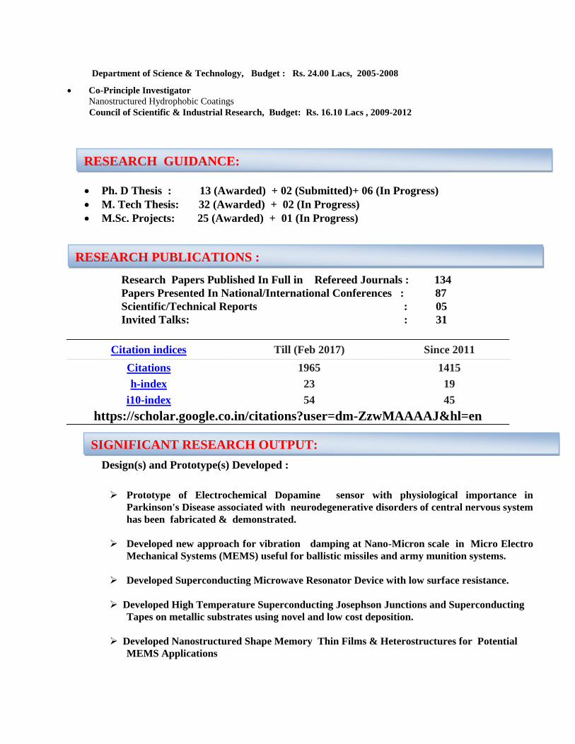
For the first time we have added a new dimension to the application of SMA thin film
heterostructures in electrochemical sensing. In the present research hard and adherent
nanostructured TiN of approximate thickness 100 nm were insitu grown to improve the texture,
electrical, mechanical and wear properties of SMA thin films without sacrificing the shape
memory effect. Further the electrodes modified with TiN/NiTi/Si heterostructure has been used
for the electrochemical sensing of Dopamine , which has a critical physiological importance
in Parkinson’s disease associated with neurodegenerative disorders of central nervous
system. The disease occurs when there is a sharp decline in dopamine level.
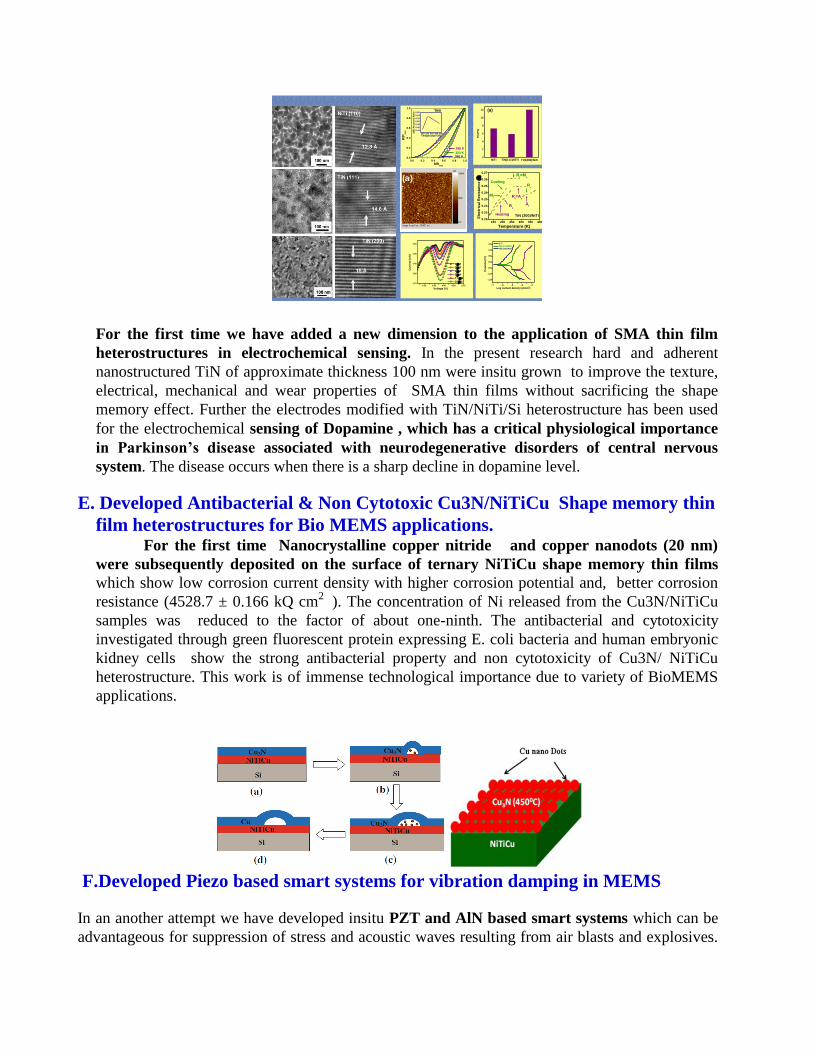
E. Developed Antibacterial & Non Cytotoxic Cu3N/NiTiCu Shape memory thin
film heterostructures for Bio MEMS applications. For the first time Nanocrystalline copper nitride and copper nanodots (20 nm)
were subsequently deposited on the surface of ternary NiTiCu shape memory thin films
which show low corrosion current density with higher corrosion potential and, better corrosion
resistance (4528.7 ± 0.166 kQ cm2
). The concentration of Ni released from the Cu3N/NiTiCu
samples was reduced to the factor of about one-ninth. The antibacterial and cytotoxicity
investigated through green fluorescent protein expressing E. coli bacteria and human embryonic
kidney cells show the strong antibacterial property and non cytotoxicity of Cu3N/ NiTiCu
heterostructure. This work is of immense technological importance due to variety of BioMEMS
applications.
F.Developed Piezo based smart systems for vibration damping in MEMS
In an another attempt we have developed insitu PZT and AlN based smart systems which can be
advantageous for suppression of stress and acoustic waves resulting from air blasts and explosives.

These heterostructures have become increasingly important for next generation ballistic missiles
and army munition system. In present study a successful vibration damping device used to mitigate
the effect of spurious vibrations was achieved by the development of a heterostructure composite
bilayer configuration composed of piezoelectric and shape memory alloy thin films. Higher
hardness (19.8 GPa), lowest coefficient of restitution (e = 0.205), highest damping capacity and
excellent figure of merit (0.751), makes them very attractive damping material for
microelectromechanical systems (MEMS).
G. Developed Ultrthin ferromagnetic shape memory thin films for magnetic
read heads and magnetic sensors For the first time the martenistic transformation behaviour of ferromagnetic shape
memory thin films has been shown to be dependent on microstructure and dimensional constraint
of the films. Below a critical grain size of 10.8 nm of the films, the complete suppression of
martensite transformation has been demonstrated. Further exchange bias and magnetocaloric
effect has been demonstrated in NiMnSb/ CrN heterostructures making them promising
candidate for refrigeration. The films were bombarded with 200 MeV Au ions and 450 keV Ar
ions in order to acquire a better control on the properties of films using ion irradiation which is
important for investigating the acceptable radiation limits for the applications of these materials
in radiation zones such as in space or nuclear reactors.
(a
)
(b
)
(c)
-
15000
-
10000
-
5000
0
0.0 0.5 1.0 1.5
vI
N
vO
UT
tI
N
tOU
T hres
~
xr
Dep
th
(nm
)
Time
(s)
NiTi/Si
-15000
-10000
-5000
0
-15000
-10000
-5000
0
1.0 0.0 0.5 1.5
Time (s)
Dep
th (
nm
)
15
µm
NiT
i
PZ
T
1/2mv2
Inden
ter
Damping
by
Twin
variants
Damping by
Piezoelectric
ity
Pendul
um
0.0 0.5 1.0 1.5
Vel
oci
ty (
mm
/s)
Time
(s)
-0.3
0
0.3
0.6
Vel
oci
ty
(mm
/s)
NiTi/PZT/Ti
Ox
0.0 0.5 1.0 1.5
-0.3
0
0.3
0.6
Time
(s)
CrTiN/NiTi/PZT/
TiOx
Vel
oci
ty
(mm
/s)
Time
(s)
0.0 0.5 1.0 1.5
-0.3
0
0.3
0.6
Low energy ion irradiation of Ni-Mn-Sn…………
Tuning of MT by low energy ion irradiation.
The diffuse rings, characteristic
of the amorphous structure, observed
in the difraction pattern can be
assigned to the amorphization of the
core of the displacement cascades.
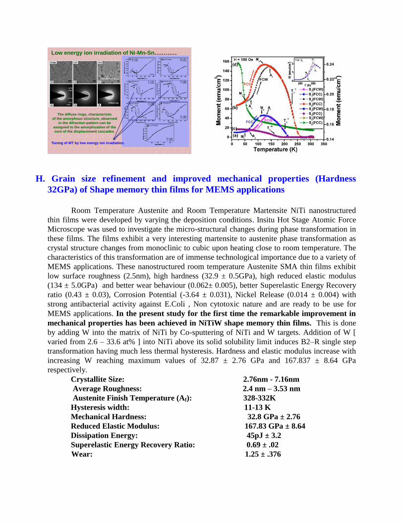
H. Grain size refinement and improved mechanical properties (Hardness
32GPa) of Shape memory thin films for MEMS applications
Room Temperature Austenite and Room Temperature Martensite NiTi nanostructured
thin films were developed by varying the deposition conditions. Insitu Hot Stage Atomic Force
Microscope was used to investigate the micro-structural changes during phase transformation in
these films. The films exhibit a very interesting martensite to austenite phase transformation as
crystal structure changes from monoclinic to cubic upon heating close to room temperature. The
characteristics of this transformation are of immense technological importance due to a variety of
MEMS applications. These nanostructured room temperature Austenite SMA thin films exhibit
low surface roughness (2.5nm), high hardness (32.9 ± 0.5GPa), high reduced elastic modulus
(134 ± 5.0GPa) and better wear behaviour (0.062± 0.005), better Superelastic Energy Recovery
ratio (0.43 ± 0.03), Corrosion Potential (-3.64 ± 0.031), Nickel Release (0.014 ± 0.004) with
strong antibacterial activity against E.Coli , Non cytotoxic nature and are ready to be use for
MEMS applications. In the present study for the first time the remarkable improvement in
mechanical properties has been achieved in NiTiW shape memory thin films. This is done
by adding W into the matrix of NiTi by Co-sputtering of NiTi and W targets. Addition of W [
varied from 2.6 – 33.6 at% ] into NiTi above its solid solubility limit induces B2–R single step
transformation having much less thermal hysteresis. Hardness and elastic modulus increase with
increasing W reaching maximum values of 32.87 ± 2.76 GPa and 167.837 ± 8.64 GPa
respectively.
Crystallite Size: 2.76nm - 7.16nm
Average Roughness: 2.4 nm – 3.53 nm
Austenite Finish Temperature (Af): 328-332K
Hysteresis width: 11-13 K
Mechanical Hardness: 32.8 GPa ± 2.76
Reduced Elastic Modulus: 167.83 GPa ± 8.64
Dissipation Energy: 45pJ ± 3.2
Superelastic Energy Recovery Ratio: 0.69 ± .02
Wear: 1.25 ± .376

I. Multiferroic Tunnel Junction of Ni50.3Mn36.9Sb12.8/BiFeO3/Ni50.3Mn36.9Sb12.8
A Multiferroic tunnel junction composed of two ferromagnetic shape memory alloy
electrodes separated by a multiferroic barrier was fabricated from Ni50.3Mn36.9Sb12.8/
BiFeO3/Ni50.3Mn36.9Sb12.8 trilayer. Large exchange bias field (HEB) of ~ 59 Oe at room
temperature was found for this trilayer. Besides the exchange bias effect in this multiferroic
tunnel junction, one of the most interesting result was magnetoelectric effect which is
manifested by the transfer of strain from Ni50.3Mn36.9Sb12.8 electrodes to BiFeO3 tunnel
barrier. The magnetic field dependence of the junction resistance was observed at room
temperature after aligning the ferroelectric polarization of BiFeO3 barrier with poling
voltage of ±3V. A change of junction resistance was also observed between the magnetic
parallel and antiparallel states of electrodes, suggesting an entire flip of the magnetic
domains against the magnetic field. After reversing the polarization of BiFeO3barrier
between the two directions, the entire R-H curve was shifted so that both parallel and
antiparallel resistances switched to different values. Hence, after applying positive and
negative voltages, two parallel and two antiparallel states, i.e., a distinct four-states were
observed. It will encode quaternary information by both ferromagnetic and ferroelectric
order-parameters, to read non-destructively by resistance measurement as shown in
following figure. The corresponding TEMR value was 17% in our MFTJ structure at room
temperature.These finding may helpful towards reconfigurable logic spintronics
architectures in next generation magneto-electric random access memory (MERAM)
devices.
-4 -2 0 2 4
11
12
13
14
15
Magnetic field (kOe)
Jun
ctio
n r
esis
tan
ce (
MΩ
)

Total Publications in Refereed Journals: 134
2017
134. Vertically arrays of Si-LaNiO3/BiFeO3/Au core-shell nano-capacitors for prominent
coupled electro-optic effect
Kirandeep Singh and Davinder Kaur
Journal of Applied Physics 121, (2017) 114103 -11
133. Room-temperature giant magnetomechanical- electric cross-coupling in Si-integrated PZT/ NiMnIn
multiferroic heterostructures
Kirandeep Singh and Davinder Kaur
J. Phys. D: Appl. Phys. 50 (2017) 145002; Impact Factor: 2.721
132. Piezoelectric control of magnetoelectric coupling driven non-volatile memory switching and self cooling effects
in FE/FSMA multiferroic heterostructures
Kirandeep Singh and Davinder Kaur
Journal of Applied Physics 121, (2017) 0841041-12
131. Room temperature magnetocaloric effect in Ni-Mn-In-Cr ferromagnetic shape memory alloy thin films
Harish Sharma Akkera, Inderdeep Singh, Davinder Kaur
Journal of Magnetism & Magnetic Materials 424, (2017) 194-198 ; Impact Factor: 2.36
2016 130. Multiferroic tunnel junction of Ni50.3Mn36.9Sb12.8/BiFeO3/Ni50.3Mn36.9Sb12.8 for magneto-electric
random access memory devices
Rahul Barman and Davinder Kaur
Applied Physics Letter 108, (2016) 092404 - 092409; Impact Factor: 3.29
129. Shape Memory alloy thin films and heterostructures for MEMS applications
Nitin Choudhary, Davinder Kaur
Sensors & Actuators: A. Physical 242 (2016) 162-181 ; Impact Factor: 2.143
128. Improved photovoltaic effect in CuO/Zn1xMgxO heterojunction solar cell by pulsed laser deposition
Rashmi Bhardwaj, Rahul Barman, Davinder Kaur
Materials Letters 185 (2016) 230–234; Impact Factor: 2.4
127. Quantification of Charge to Strain Mediated Interface Coupling Transfiguration in FE/FSMA Heterostructures
Kirandeep Singh, Davinder Kaur
Journal of Physics D: Applied Physics 49 (2016) 035004 ; Impact Factor: 2.721
126. Improved electrical transport properties in high quality nanocrystalline silicon carbide (nc-SiC) thin films for
microelectronic applications
Narendra Singh, Kirandeep Singh, Akhilesh Pandey, Davinder Kaur
Materials Letters 164 (2016) 28-31; Impact factor: 2.489
125. Tunable multiferroic properties of Mn substituted BiFeO3 thin films
Kirandeep Singh, S.K.Singh, Davinder Kaur
Ceramic International 42 (2016) 13333-14298; Impact factor: 3.02
124. Dislocation density investigation on MOCVD-grown GaN epitaxial layers using wet selective etching
Akhilesh Pandey, Brajesh S. Yadav, D. V. Sridhara Rao, Davinder Kaur, Ashok Kumar Kapoor
Applied Physics A (2016) 122:614

123. Growth and evolution of residual stress of AlN films on silicon (100) wafer
Akhilesh Pandey , Shankar Dutta, Ravi Prakash , Sandeep Dalal , R. Raman , A.K. Kapoor, Davinder Kaur
Materials Science in Semiconductor Processing 52 (2016) 16–23.
122. Structural, corrosion, and mechanical properties of sputtered deposited chromium tungsten nitride (Cr1-
xWxN) nanocomposite thin films
Ravi Prakash, R. Jayaganthan and Davinder Kaur
Advanced Material Letters 7 (2016) 100-150
121. Effect of Cr addition on the structural, magnetic and mechanical properties of magnetron sputtered Ni–Mn–In
ferromagnetic shape memory alloy thin films
Harish Sharma Akkera, Davinder Kaur
Applied Physics A (2016) 122:996
2015
120. Direct and converse magneto-electric coupling in ferromagnetic shape memory alloys based thin film
multiferroic heterostructures.
Kirandeep Singh and Davinder Kaur
Applied Physics Letter 107, (2015) 262901-262905; Impact Factor: 3.29
119. Manifestation of martensitic phase transformation and magneto-caloric properties in high quality
magnetron sputtered Ni-Mn-In/Si ultra thin films
Kirandeep Singh, Davinder Kaur
Sensors & Actuators: A. Physical 236 (2015) 247-256 ; Impact Factor: 2.143
118. Structural phase transition and enhanced ferroelectricity in Bi(Fe1-xMnx)O3 thin films deposited by Pulsed
Laser deposition
Rahul Barman, S.K. Singh, Davinder Kaur
Thin Solid Films 594 (2015) 80-87 ; Impact factor: 2.038
117. Structural and Optical properties of (ool) oriented Vanadium Pentaoxide Nanorods
Vibhu Goyal, Nitin Choudhary, Kirandeep Singh, Davinder Kaur
Nanomaterials and Energy 3 February (2015) 1-10
116. Vibration Damping Materials and Their Applications in Nano/Micro-Electro-Mechanical Systems:
Nitin Choudhary and Davinder Kaur
Journal of Nanoscience and Nanotechnology Vol. 15, March (2015) 1907-1924
115. Martensitic phase transformation of magnetron sputtered nanostructured Ni-Mn-In ferromagnetic shape
memory alloy thin films
Harish Sharma Akkera, Inderdeep Singh and Davinder Kaur
Journal of Alloys and Compounds 642 (2015) 53–62; Impact factor: 2.999
114. Martensitic phase transformations and magnetocaloric effect in Al co-sputtered Ni–Mn–Sb alloy thin films
Harish Sharma Akkera, Nitin Choudhary and Davinder Kaur
Materials Science and Engineering B 198 (2015) 113–119; Impact factor: 2.122
113. Leakage current behavior of BiFeO3/BiMnO3 multilayer fabricated by pulsed laser deposition
Rahul Barman, Davinder Kaur
Journal of Alloys and Compounds 644 May (2015) 506–512; Impact factor: 2.999

112. Improved magnetocaloric effect in magnetron sputtered NiMn-Sb-Al ferromagnetic shape memory alloy
thin films
Rahul Barman, Davinder Kaur
Vacuum 120 October (2015) 22-26; Impact factor: 1.858
111. Electrical, Surface Morphology and Magneto-capacitance Properties of Pb free Multiferroic
(BiFeO3)1−x(BaTiO3)x Solid Solutions
M. Shariq, D. Kaur, V. S. Chandel and M. A. Siddiqui
Acta Physica polonica A, 127 (2015) 1675-1679
110. Structural and optical properties of pulsed laser deposited ZnO/TiO2 and TiO2/ZnO thin films
Praveen K. Jain, Mohammad Salim, Davinder Kaur
Optik-International Journal for Light and Electron Optics 126 (2015) 3260-3262.
2014
109. Strain mediated coupling in magnetron sputtered multiferroic PZT/Ni-Mn-In/Si thin film heterostructure
Kirandeep Singh, Sushil Kumar Singh, and Davinder Kaur
Journal of Applied Physics 116, September (2014) 114103-9 ; Impact factor: 2.259
108. Enhanced exchange bias in magnetron-sputtered Ni–Mn–Sb–Al ferromagnetic shape memory thin films
Rahul Barman, Sushil Kumar Singh, Davinder Kaur
Current Applied Physics14 December (2014 )1755-1759; Impact factor: 2.212
107. Room temperature nanoindentation creep of nanograined NiTiW shape memory alloy thin films
Navjot Kaur, Davinder Kaur
Surface Coating Technology 260 December (2014) 260-265; Impact factor: 2.453
106. Thickness dependent exchange bias in co-sputter deposited Ni-Mn-Al Heusler alloy nanostructured thin films
A. Mishra, S.K. Srivastava, , A. Kumar, P. Dubey, S. Chauhan, Amit Kumar, D. Kaur, R.Chandra
Thin Solid Films 572 December (2014) 142-146; Impact factor: 2.038
105. NiTiCu/AlN/NiTiCu shape memory thin film heterostructures for vibration damping in MEMS
Navjot Kaur, Davinder Kaur
Journal of Alloys and Compounds 590 March (2014) 116–124; Impact factor: 2.999
104. Electrical transport behavior of lead-free BZT-BCT thin film grown on LaNiO3/Si by laser deposition
Chandan Bhardwaj, Davinder Kaur
Journal of Alloys and Compounds 595 May (2014) 158-163 ; Impact factor: 2.999
2013
103. Exchange bias effect in NiMnSb/CrN heterostructures deposited by magnetron sputtering
Harish Sharma, Rahul Barman, Navjot Kaur, Nitin Choudhary, and Davinder Kaur
Journal of Applied Physics 113, 17D723 May (2013) ; Impact factor: 2.259
102. NiTi/Pb(Zr 0.52Ti 0.48)O3 thin film heterostructures for vibration damping in MEMS
Nitin Choudhary, D.K. Kharat, J. Van Humbeeck, Davinder Kaur
Sensors and Actuators A 193 April (2013) 30– 34; Impact factor: 2.143
101. Magnetron sputtered Cu3N/NiTiCu shape memory thin film heterostructures for MEMS applications.
Navjot Kaur , N. Choudhary, Rajendra N. Goyal, S. Viladkar, I.Matai, P.Gopinath, S.Chokalingam and
Davinder kaur
Journal of Nanoparticle Research 15 April (2013) 1468; Impact factor: 2.278

100. Structural and magnetic properties of La2NiMnO6 thin films on LaAlO3 substrate with varying thickness
Deepak Kumar and Davinder Kaur
Journal of Alloys and Compounds 554 March (2013) 277- 283; Impact factor: 2.999
99. Electrochemical investigations of mometasone furoate, a corticosteroid, in micellar medium
Rajendra N. Goyal, Davinder Kaur , Bharati Agrawal , Saurabh Kumar Yadav
Journal of Electroanalytical Chemistry 695 (2013) 17–23; Impact factor: 2.676
98. Energetic ion irradiation induced crystallization of Ni-Mn-Sn ferromagnetic shape memory thin film
R. Vishnoi, R. Singhal, K. Asokan, J.C. Pivin, D. Kanjilal, D. Kaur
Vacuum 89 March (2013) 190-196 ;Impact factor: 1.858
97. Grain refinement of NiTi shape memory alloy thin films by W addition
Navjot Kaur , Davinder kaur
Material Letters 91 January (2013) 202-205; Impact factor: 2.489
96. Pulsed laser deposition and characterization of highly tunable BZT-BCT grown on LaNiO3/Si substrate
Chandan Bhardwaj , B.S.S. Daniel , Davinder Kaur
Journal of Physics and Chemistry of Solids 74 January (2013) 94-100; Impact factor: 1.527
95. Electronic excitation induced phase transformation in FSMA thin film
R. Singhal , R. Vishnoi , K. Asokan , D. Kanjilal , D. Kaur
Vacuum 89 March (2013) 215-219;Impact factor: 1.858
94. Investigation on multiferroic properties of BiFeO3 ceramics
M. SHARIQ, D. KAUR, M.A. SIDDIQUI
Materials Science-Poland, 31(3), 2013, pp. 471-475
2012
93. Effect of Ti addition on the structural, mechanical and damping properties of magnetron sputtered Ni-Mn-Sn
ferromagnetic shape memory alloy thin films
Nitin Choudhary, Davinder Kaur
Journal of Physics D: Applied Physics 45 Dec(2012) Issue 49 495304; Impact factor: 2.721
92. Highly tunable compositionally graded BZT-BCT multilayer with low temperature capacitance coefficients
Chandan Bhardwaj , B.S.S. Daniel , Davinder Kaur
Materials Letters 87 November (2012) 172–175; Impact factor: 2.489
91. Variation in phase transformation paths of NiTi films as a function of film thickness
Ashvani Kumar, Devendra Singh, Davinder Kaur
Sensors and Actuators A 178 May (2012) 57– 63 ; Impact factor: 2.143
90. Phase transformation in Ni-Mn-Sn ferromagnetic shape memory alloy thin films induced by dense ionization
R. Vishnoi, R. Singhal, K. Asokan, D. Kanjilal and Davinder Kaur
Applied Physics A : Material Science 107 June (2012) 925–934 ; Impact factor: 1.694.
89. Relaxor characteristics of highly tunable BZT-BCT thin film grown on LaNiO3/Si by pulsed laser deposition,
Chandan Bhardwaj, Davinder Kaur
Current Applied Physics 12 September (2012) , 1239-1243 ; Impact factor: 2.212.
88. Improved electrical and mechanical properties of NiTi/TiOx/PZT/TiOx thin film heterostructures
Nitin Choudhary, D. K. Kharat, Davinder Kaur
Solid State Phenomena Vol. 185 (2012) 25-27
87. Influence of buffer layer on structural, electrical and mechanical properties of PZT/NiTi heterostructures
Nitin Choudhary, Davinder Kaur
Journal of Alloys and Compounds 536 September (2012) 56-65; Impact factor: 2.999
86. Independent gate SRAM based on asymmetric gate to source/drain overlap-underlap device FinFET
N Kaushik, BK Kaushik, D Kaur, MK Majumder
Progress in VLSI Design and Test, (2012) 373-374
2011
85. Surface modification of NiTi/PZT heterostructures using various protective layers for potential MEMS
applications
Nitin Choudhary, D.K. Kharat and Davinder Kaur
Surface and Coatings Technology, 206 December (2011) 1735; Impact factor: 2.453.
84. Ion irradiation induced modifications of nanostructured Ni–Mn–Sn ferromagnetic shape memory thin films
R. Vishnoi , R. Singhal , K. Asokan , D. Kanjilal, Davinder Kaur,
Thin Solid Films 520 December (2011) 1631–1637; Impact factor: 2.038
83. Thickness dependent phase transformation of magnetron-sputtered Ni–Mn–Sn ferromagnetic shape memory
thin films
Ritu Vishnoi, Rahul Singhal & DavinderKaur
Journal of Nanoparticle Research 13 September (2011) 3975- 3990; Impact factor: 2.278.
82. Exchange bias behaviour in magnetron sputtered Ni 49.8 Mn 36.1Sn13. ferromagnetic shape memory thin
film
Ritu Vishnoi, Davinder Kaur
Journal Of Alloys And Compounds 509 February (2011) 2833–2837; Impact factor: 2.790.
81. Structural, electrical and mechanical properties of magnetron sputtered NiTi/PZT/TiOx thin film
heterostructures
Nitin Choudhary, D.K. Kharat, Davinder Kaur
Surface & Coatings Technology 205 February (2011) 3387–3396; Impact factor: 2.453.
80. Effect of oxygen partial pressure and VO2 content on hexagonal WO3 thin films synthesized by pulsed laser
deposition technique
Ajay Kaushal and Davinder Kaur
Journal of Nanoparticle Research 13 June (2011) 2485–2496 ; Impact factor: 2.278.
79. Pulsed laser deposition of transparent ZnO/MgO multilayers
Ajay Kaushal, Davinder Kaur
Journal Of Alloys And Compounds 509 January (2011) 200–205; Impact factor: 2.999.
78. Influence of reactive gas on structural properties of magnetron sputtered CrSiN coatings
Hetal N. Shah, R. Jayaganthan, Davinder Kaur
Applied Surface Science 257April (2011) 5535–5543; Impact factor: 2.538.
77. Influence of Mo Concentration on Properties of Pulsed Laser Deposited Nanostructured Sr2FeMoxW1−x O6
Deepak Kumar and Davinder Kaur
Advanced Science Letters, Vol. 4, January (2011) 29-35.
76. VO2–WO3 nanocomposite thin films synthesized by pulsed laser deposition technique
Ajay Kaushal, Nitin Choudhary, Navjot Kaur, Davinder Kaur
Applied Surface Science 257 August (2011) 8937-8944; Impact factor: 2.71.
75. Exchange biasing in SFMO/SFWO double perovskite multilayer thin films
Deepak Kumar, Davinder Kaur
Journal of Alloys and Compounds 509 July (2011) 7886– 7890; Impact factor: 2.999.
74. Fingerprint recognition using image segmentation
Sangram bana, N.Ahlawat and Davinder Kaur
International Journal of Advanced Engineering Sciences and Technologies 9 (2011), 146-158
73. Antiferromagnetic thickness dependence of blocking temperature in SFMO/SFWO multilayer
Deepak Kumar, Davinder Kaur
Materials Chemistry and Physics 129 October (2011) 802– 804; Impact factor: 2.427.
72. Structural, optical & magnetic properties of Nd-doped BiFeO3 films prepared by pulsed laser
Anshu Gaur, Kirandeep Singh, Navjot Kaur and Davinder Kaur
Physica B 406 May (2011) 1877–1882; Impact factor: 1.327.
71. 200 Mev Ag+ Ion Beam Induced Modifications In AgInSe2 Films Deposited By Hot Wall Vacuum
Evaporation
Dinesh Pathak, R. K. Bedi, Davinder Kaur
Chalcogenide Letters Vol. 8, March (2011), 213 – 222.
70. Structural, optical and magnetic properties of Bi0.9-ySmyLa 0.1FeO3 thin films deposited by laser deposition
technique
Ajay Kaushal, Neeraj Kumar and Davinder Kaur
Optoelectronics And Advanced Materials Vol. 5, May (2011), 545 – 550.
69. Image segmentation schemes applied to microscopic images
Sangram bana, N.Ahlawat and Davinder Kaur
International Journal of Advanced Engineering Sciences and Technologies 9 (2011), 146-158
2010
68. Structural and magnetic properties of magnetron sputtered Ni–Mn–Sn ferromagnetic shape memory thin films
Ritu Vishnoi and Davinder Kaur
Journal of Applied Physics 107, May (2010) 103907; Impact factor: 2.259.
67. Size dependence of martensite transformation in nanostructured Ni–Mn–Sn ferromagnetic shape memory
Ritu Vishnoi, Davinder Kaur
Surface & Coatings Technology 204 August (2010) 3773–3782; Impact factor: 2.453.
66. Influence of sputtering parameters and gases on microstructure of Chromium Nitride films
Hetal N. Shah, R. Jayaganthana, Davinder Kaur
Thin Solid Films 518 August (2010) 5762-5768; Impact factor: 2.038.
65. Influence of silicon content on the microstructure and hardness of CrN coatings
deposited by reactive magnetron sputtering
Hetal N. Shah, R. Jayaganthana, Davinder Kaur
Materials Chemistry And Physics 121 June (2010) 567–571; Impact factor: 2.427.
64. Microstructural Characterization of CrN thin films deposited on stainless steel by magnetron sputtering
Hetal N. Shah, R. Jayaganthan, Davinder Kaur
Bulletin of Material Science (springer) 33 April (2010) 103-110.
63. Substrate Dependent Structural and Magnetic Properties of Pulsed Laser Deposited Fe3O4 Films
Rajendra N. Goyal, Ashish K.Pandey, and Davinder Kaur
Journal Of Nanoscience And Nanotechnology, 10, Dec (2010), 8018-8025; Impact factor: 2.149.
62. Effect of Substrate Temperature on the Structural, Optical, and Electrical Properties of AgInSe by PLD
Dinesh Pathak, and R. K. Bedi, and Davinder Kaur
Journal of the Korean Physical Society, 56, NO. 3, (2010), 836-841.
61. Room temperature growth of nanocrystalline anatase TiO2 thin films by dc magnetron sputtering
Preetam Singh, Davinder Kaur
Physica B 405 March (2010) 1258–1266; Impact factor: 1.327.
60. Effect of La doping on structural, optical and magnetic properties of BiFeO3 deposited by laser technique
N. kumar, C. Bhardwaj, D. KAUR
Optoelectronics And Advanced Materials – Rapid Comm. Vol. 4, No. 10, (2010) , 1497 - 1502
59. Crystalline Aginse 2 Films On Glass By Laser Ablation
D Pathak, RK Bedi, A Kaushal, D Kaur
International Journal of Modern Physics B 24 (27), (2010) 5379-5385
58. Voltammetric Sensor Based on Nano TiO2 Powder Modified Glassy Carbon Electrode
Rajendra N. Goyal, Ashish K. Pandey and Davinder Kaur
The Open Chemical and Biomedical Methods Journal, 2010, 3, 66-73
57. Substrate-dependent structural and magnetic properties of Sr2FeMoO6 nanostructured perovskite
Deepak Kumar, Davinder Kaur
Physica B 405 August (2010) 16, 3259-3266; Impact factor: 1.327.
56. Structural, optical and dielectric properties of ZnTiO3 ceramics
P. K. Jain, D. Kumar, A. Kumar, D. Kaur
Optoelectronics and Advanced Materials Vol. 4, No.3, (2010), 299-304.
55. Fabrication of Densely Distributed Silver Indium Selenide Nanorods by Using Ag+ Ion
Irradiation
Dinesh Pathak, R. K. Bedi, and Davinder Kaur
Journal of the Korean Physical Society, 57, No. 3, (2010), 474-479.
54. Characterization of AgInSe2 Films Deposited by Hot-Wall Vacuum Evaporation Method
Dinesh Pathak; R. K. Bedi; Davinder Kaur
Materials And Manufacturing Processes, 25: (2010), 1012–1017
53. Effect of sputtering pressure and temperature on DC magnetron sputtered CrN films
H. N. Shah, R. Jayaganthan and Davinder Kaur
Surface Engineering 26 (2010) 629-637 .
52. Mechanical properties of nanostructured copper/hydrogenated amorphous multilayer films grown in a low
vacuum system
Neeraj Dwivedi, Sushil Kumar, Davinder Kaur, C. M. S. Rauthan, O. S. Panwar
Optoelectronics and Advanced Materials Vol. 4, No.4, (2010), 604-910.
51. Growth Of AgInSe 2 On Si (100) Substrate By Pulse Laser Ablation
D Pathak, RK Bedi, D Kaur
Surface Review And Letters 16 (06), (2010) 917-
2009
50. Nanoindentation and corrosion studies of TiN/NiTi thin films for biomedical applications
Ashvani Kumar and Davinder Kaur
Surface and Coatings Technology 204 December (2009) 1132-1136; Impact factor: 2.453.
49. Structural, electrical and optical properties of transparent Zn1-xMgxO nanocomposite thin films
Ajay Kaushal, Dinesh Pathak, R.K.Bedi and Davinder Kaur
Thin Solid Films 518 December (2009) 1394–1398; Impact factor: 2.038
48. Room-temperature ferromagnetism in Sn1-xMnxO2 nanocrystalline films by ultrasonic pyrolysis
Ajay Kaushal, Prerna Bansal, Ritu Vishnoi, Nitin Choudhary and Davinder Kaur
Physica B: Condensed Matter 404 November (2009) 3732-3738; Impact factor: 1.327.
47. Growth and characterization of iron oxide nanocrystalline films via low-cost ultrasonic Pyrolysis
R. N. Goyal, Ashish K. Pandey and Davinder Kaur
Materials Chemistry and Physics, 116 (2) August (2009) 638-644; Impact factor: 2.427.
46. Growth of AgInSe2 on Si (100) substrate by thermal evaporation technique
Dinesh Pathak , R. K. Bedi and Davinder Kaur
Appl Physics A: Material Science and Processing 95 June (2009) 843-847; Impact factor: 1.694.
45. Effect of crystallographic orientation of nanocrystalline TiN on electrical & mechanical properties of
TiN/NiTi films
Ashvani Kumar, Devendra Singh, Ravi Kumar and Davinder Kaur
Journal of Alloys and Compounds 479 1-2 June (2009) 166-172; Impact factor: 2.999.
44. Fabrication and nanoindentation properties of TiN/NiTi and applications in electrochemical sensing
Ashvani Kumar, Devendra Singh, Rajendra N Goyal and Davinder Kaur
Talanta 78 May (2009) 964-969; Impact factor: 3.756.
43. Grain size effect on structural, electrical and mechanical properties of NiTi thin films deposited by sputtering
Ashvani Kumar, Devendra Singh and Davinder Kaur
Surface & Coatings Technology 203 March (2009) 1596-1603; Impact factor: 2.453
42. Mn-Doped ZnO Nanocrystalline Thin Films Prepared by Ultrasonic Spray Pyrolysis
Preetam Singh, Ajay Kaushal and Davinder Kaur
Journal of Alloys and Compounds 471 March (2009) 11-15; Impact factor: 2.790.
41. Effect of Mg content on structural, electrical and optical properties of pulsed laser deposited Zn 1-X MgxO
nanocomposite thin films
Ajay Kaushal and Davinder Kaur
Solar Energy Materials & Solar Cells 93 February (2009) 193–198; Impact factor: 5.755.
40. Fabrication of Fe2O3 nanopowder modified glassy carbon electrode for applications in electrochemical sensing
Rajendra Goyal, A. K. Pandey, Ashvani Kumar and Davinder Kaur
Journal of Nanoscience and Nanotechnology 9 (3) (2009) 1278.
2008
39. Influence of film thickness on texture, electrical and optical properties of room temperature deposited
nanocrystalline V2O5 films
Preetam Singh and Davinder Kaur

Journal of Applied Physics 103 (2008) 043507; Impact factor: 2.259.
38. Intrinsic magnetism in Zn 1-x Cox O (0.03 > x < 0.10) thin films prepared by ultrasonic spray pyrolysis
Preetam Singh, Deepak, A. K Pandey and Davinder Kaur
Journal of Physics.: Condensed Matter 20 (2008) 315005; Impact factor:2.355.
37. Structural and optical studies of nanocrystalline V2O5 thin films
Ashvani kumar, Preetam Singh and Davinder Kaur
Thin Solid Films 516 (2008) 912-918; Impact factor: 2.038.
36. ZnO nanocrystalline powder synthesized by ultrasonic mist-chemical vapour deposition
Preetam Singh, Ashvani Kumar, Deepak and Davinder Kaur
Optical Materials 30 (2008) 1316-1322; Impact factor: 2.075.
35. Effect of graphite and metallic impurities of C60 on determination of salbutamol in biological fluids
Rajendra N. Goyal , A. K. Pandey, Preetam Singh and Davinder Kaur
Talanta 75 (2008) 63–69; Impact factor: 3.756.
34. Insitu high temperature XRD studies of ZnO nanopowder
Preetam Singh and Davinder Kaur
Bulletin Material Science 31 (2008) 573-577.
33. Substrate effect on texture properties of nanocrystalline TiO2 thin films
Preetam Singh, Ashvani Kumar and Davinder Kaur
Physica B 403 (2008) 3769-3773; Impact factor: 1.327.
32. Structural and optical properties of AgInSe2 films
R. K. Bedi, D. Pathak, Deepak and Davinder Kaur
Zeitschrift für Kristallographie Supplements 27 (2008) 177-183
2007
31. Growth and characterization of ZnO nanocrystalline thin films and nanopowder via low cost ultrasonic spray
pyrolysis Preetam Singh, Ashvani Kumar, Deepak and Davinder Kaur
Journal of Crystal Growth 306 (2007) 303-310; Impact factor: 1.752.
30. Structural and optical characterization of ZnO nanocrystalline films
A. K. Chawla, R. Chandra and Davinder Kaur
Optical Materials 29 (2007) 995-998; Impact factor: 2.075.
29. Effect of oxygen partial pressure on the structural and optical properties of sputter deposited zinc oxide films
Preetam Singh, Amit Kumar Chawla, Davinder Kaur, R.Chandra
Material Letters 61 (2007) 2050-2053; Impact factor: 2.224.
28. Structural, electrical and magnetic properties of PrBaMnO3
Neeraj Panwar, S. K. Agarwal, G. L. Bhalla and Davinder Kaur
International Journal of Modern Physics B 21, 15 (2007) 2647-2656.
2006
27. Texture development in Ti-Si-N nanocomposite thin films
R. Chandra, Davinder Kaur, N. Phinichka and Z. H. Barber
Material Science & Engineering A 423 (2006) 111-115; Impact factor: 2.590.
26. Low cost synthesis of high-Tc superconducting films on metallic subs by ultrasonic spray pyrolysis
Ashvani Kumar, Preetam Singh and Davinder Kaur
Cryogenics 46 (2006) 749-758.
25. Electronic transport studies of rare earth nickletes (RNiO3) prepared by pulsed laser deposition
Ashvani Kumar, Preetam Singh and Davinder Kaur
Journal of Physics D: Applied Physics 39 (2006) 5310-5315; Impact factor: 2.721.
2005
24. Microwave characterization of laser ablated YBCO thin films
Davinder Kaur
Cryogenics 45 (2005) 455-462.
23. Pulsed laser deposition of NdNiO3 thin films
Davinder Kaur, J. Jesudasan and Pratap Raichaudhary
Solid state communication 136, (2005), 369-374; Impact factor: 1.781.
22. Structural, optical and electronic properties of nanocrystalline TiN films
R. Chandra, A. K. Chawla Davinder Kaur and P.Ayyub
Nanotechnology 16 (2005) 3053-3056; Impact factor: 3.842.
2004
21. Microstructure and temperature dependence of penetration depth of Ag-YBCO films
Davinder Kaur, S. P. Pai, J. Jesudasan and R. Pinto
Physica C: Superconductivity 405 (2004) 96-102.
2003
20. Metal-Insulator transition in BaRuO3 thin films
Davinder Kaur and K. V. Rao
Journal of Physics D: Applied Physics 36 (2003) 156-159; Impact factor: 2.721.
19. Microstructural & conductive properties of epitaxial BaRuO3 thin films
Davinder Kaur and K. V. Rao
Solid State Communication 128 (2003) 391-395; Impact factor: 1.781
2002
18. Grain boundary Josephson Effect in BSCCO microbridges
Davinder Kaur and A. K. Gupta
Journal of Physics D: Applied Physics 35 (2002) 729-731 ; Impact factor:2.528.
1998
17. Microwave penetration depth measurements of Ag-YBCO thin films
Davinder Kaur, R. Pinto and H. W. Weber
Solid State Communication 106 (1998) 231-234; Impact factor: 1.781.
16. Thickness and microstructural dependence of microwave surface resistance in Ag-YBa2Cu3O7-
Davinder Kaur, John Jesudassan, C. P. D’Souza and R. Pinto
Applied Superconductivity 6 (1998) 45-48.
1996
15. Microstructural dependence of penetration depth of YBCO thin films probed by atomic force microscopy
R. Pinto, Davinder Kaur, P. R. Apte, M. S. R. Rao and R. Vijayaraghavan
Applied Physics Letter 68 (1996) 1720-1722; Impact factor: 3.794.
1994
14. Preparation of high quality BSCCO thin films by spray pyrolysis
Davinder Kaur and A. K. Gupta
Indian Journal of Pure & Applied Physics 32 (1994) 147-151.
1993
13. Optimization of deposition and annealing parameters for preparation of high quality YBCO thin films
Davinder Kaur and A. K. Gupta
Indian Journal of Pure & Applied Physics 31 (1993) 696-701.
1991 12. Grain boundary Josephson Effects in YBCO films
D. K. Walia and A. K. Gupta
Superconductor Science & Technology 4 (1991) 650 ; Impact factor: 2.758.
11. Study of Josephson Effects in the microbridges made on BSCCO films.
D. K. Walia, A. K. Gupta, G.S.N Reddy, V.N.Ojha, V.S.Tomar, N.Khare, N. D. Kataria ,K.C.Nagpal
Bulletin of Material Sciences 14 (1991) 1119-1123.
10. Effective passivation of YBCO superconducting bridges
G. S. N. Reddy, A. K. Gupta, V. S. Tomar, N.Khare, N.D.Kataria ,V.N.Ojha and D.K.Walia
Cryogenics 31 (1991) 209-211.
9. Study of Galvanomagnetic Effects in Bi-Sr-Ca-Cu-O films.
Ramesh Chandra, N. Khare, A.k.Gupta, D. K. Walia , S. Chaudhary, V.N.Ojha, V.S.Tomar
Bulletin of Material Sciences 14 (1991) 1163-1166.
8. Observation of SQUID behaviour in high temperature superconductors
G. S. N. Reddy, D. K. Walia, V. S. Tomar , N. Khare, N. D. Kataria and A. K. Gupta
Indian Journal of Physics 61 (1991) 43-49; Impact factor: 1.785.
1990 7. Growth of oriented superconducting films of BSCCO by spray pyrolysis technique
D. K. Walia, A. K. Gupta, N. D. Kataria, N.Khare,V.N.Ojha and V. S. Tomar
Modern Physics Letters B 4 (1990) 393.
6. Laser Patterning of Microbridges and DC SQUID Structure on BSCCO Films.
N. Khare, A. K. Gupta, D. K. Walia, V. N. Ojha,V. S. Tomar,Y. K. Jain
Superconductor Science & Technolology 3 (1990) 191; Impact factor: 2.758.
5. Microwave frequency and power dependence of critical currents in microbridges of BSCCO films
V. N. Ojha, V. S. Tomar, A. K. Gupta, D. K. Walia and G. S. N. Reddy
Physica B 167 (1990) 1607-1608; Impact factor: 1.327.
4. Quantum interference effects in laser patterned BSCCO films
A. K. Gupta, N. Khare, D. K. Walia, V. S. Tomar,V N Ojha, H C Pandey, S K Bhatnagar,
Pramana-Journal of Physics 35 (1990) L193-L198.

1989
3. Superconductivity in BSCCO films made by spray pyrolysis D. K. Walia, A. K. Gupta, GSN Reddy, V. S. Tomar, N. D. Kataria, V N Ojha and N.Khare Solid State Communications 71 (1989) 987-990; Impact factor: 1.781. 2. Low resistance silver contacts on BSCCO films N. Khare,D. K. Walia, GSN Reddy, V. N. Ojha,N D Kataria, V. S. Tomar and A. K. Gupta
Journal of Physics D: Applied Physics 22 (1989) 1237-1240 ; Impact factor: 2.528. 1. Growth of superconducting films of YBCO by spray pyrolysis and study of quantum interference effects G. S. N. Reddy, A. K. Gupta, V.N. Ojha, N.D. Kataria, N.Khare, D. K. Walia and V. S. Tomar Modern Physics Letters B 3 (1989) 1311-1314.
Related Documents