IEEE TRANSACTIONS ON INDUSTRIAL ELECTRONICS, VOL. 51, NO. 2, APRIL 2004 419 Current Distribution Control Design for Paralleled DC/DC Converters Using Sliding-Mode Control Mariano López, Luis García de Vicuña, Member, IEEE, Miguel Castilla, Pedro Gayà, and Oscar López Abstract—This paper shows the analysis and design of a parallel-connected converter system using sliding mode control techniques. The design is particularised for a system that consists of boost converters and a current feedback loop based on a proportional–integral compensator of the output voltage error. The paper emphasises the advantages of the sliding-mode control over the classic design method based on small-signal models, thus providing an effective and robust means of controlling nonlinear multi-input converters. The design is based on the Utkin conditions, which permit us to know the regions under which a sliding mode exists. This fact allows us to design the compensator and to introduce some modifications in the control loop that avoids input-current overshoots during the system startup. Simple design expressions are obtained and verified with simulation and experimental results, thus showing the improvements achieved with the proposed modifications. Index Terms—DC–DC power conversion, power control, vari- able-structure systems. I. INTRODUCTION T HE use of dc-to-dc converters connected in parallel is a suitable way to solve the technological problems that arise in large-capability power supply systems. This arrangement en- sures the supply of high output currents with high reliability in applications such as mainframe computers and, systems using very large scale integration technology (VLSI) and uninterrupt- ible power supplies (UPS) [1]. For the effectiveness of the parallel system the control must ensure both the equal sharing of the load current among the converters and the regulation of the output voltage. Recently, different current-control schemes for achieving these aims have been proposed [2]–[6]. Basically, the output voltage is regulated by an outer voltage loop, while the equalization of the load current is normally attained by adding an inner current loop which compares the current supplied by each module with a reference current. A democratic control scheme arises when this current is the average of the output currents supplied by the modules [2]–[4]. In master–slave control the reference current corresponds to the output current of a module called master [5], [6]. Traditionally, all these control schemes have been designed after studying the phase margin of the loop gain deduced from a small-signal model of a nonlinear plant [2]–[4]. A large number of small-signal transfer functions must be dealt with, raising the complexity of the analysis and providing tedious expres- Manuscript received November 26, 2001; revised February 7, 2003. Abstract published on the Internet January 13, 2004. The authors are with the Universitat Politècnica de Catalunya, 08800 Vilanova i la Geltrú, Spain (e-mail: [email protected]). Digital Object Identifier 10.1109/TIE.2004.825273 sion of the closed-loop gain. In such cases, it is easier to design the controller by means of computer simulations, thus obtaining discrete values for the constants of the compensator. However, the design must be returned when load or power stage parame- ters variations are produced, since the small-signal model is de- duced by linearising about a given steady-state operating point or trajectory. Sliding-mode control is an alternative method of designing the control loop of parallel systems controlled by democratic or master-slave current-control schemes. Essentially, the sliding-mode control utilizes a high-speed switching control law to drive the nonlinear state trajectory onto a specified sur- face in the state space, called the sliding or switching surface, and to maintain it on this surface for all subsequent time [10]. The main feature of the sliding mode is the robustness that the system acquires against disturbances in the load and in the input voltage [11], [12]. This paper presents a simple way to design the compensator of a democratic current-control scheme using sliding-mode con- trol. The process can also be extended to a master–slave scheme. The presented design procedure shows an example based on a proportional–integral compensator applied to boost con- verters connected in parallel. The paper also shows how the sliding-mode control allows us to overcome some of the disad- vantages that appear within the classic design method based on small-signal models. Simplicity is one of the main advantages of a sliding-mode design, since it is not necessary to handle complex transfer functions. Moreover, by studying the sliding domain, simple modifications can be introduced in the compen- sator that improve the dynamic behavior of the system, espe- cially in the startup, producing soft waveforms in the input cur- rent and output voltage. II. REVIEW OF THE DESIGN PROCESS BASED ON SMALL-SIGNAL MODELS This section presents a summarized review of the control de- sign of parallel systems by means of small-signal models. Fig. 1 shows the power stage and control loops for this system partic- ularised for three boost converter modules. For the sake of sim- plicity, and without an essential loss of generality, losses related to semiconductors, capacitors, and inductors are neglected. The diode and the resistance are not considered in the analysis since they only work in the startup. The function repre- sents the proportional–integral compensator and stands for the gain of the current-sensing network. Linear control techniques have been extensively applied to design the function , as it is described in [2]–[4]. Let us briefly sum up the main steps involved in this design. 0278-0046/04$20.00 © 2004 IEEE

Welcome message from author
This document is posted to help you gain knowledge. Please leave a comment to let me know what you think about it! Share it to your friends and learn new things together.
Transcript
IEEE TRANSACTIONS ON INDUSTRIAL ELECTRONICS, VOL. 51, NO. 2, APRIL 2004 419
Current Distribution Control Design for ParalleledDC/DC Converters Using Sliding-Mode Control
Mariano López, Luis García de Vicuña, Member, IEEE, Miguel Castilla, Pedro Gayà, and Oscar López
Abstract—This paper shows the analysis and design of aparallel-connected converter system using sliding mode controltechniques. The design is particularised for a system that consistsof boost converters and a current feedback loop based on aproportional–integral compensator of the output voltage error.The paper emphasises the advantages of the sliding-mode controlover the classic design method based on small-signal models,thus providing an effective and robust means of controllingnonlinear multi-input converters. The design is based on the Utkinconditions, which permit us to know the regions under which asliding mode exists. This fact allows us to design the compensatorand to introduce some modifications in the control loop thatavoids input-current overshoots during the system startup. Simpledesign expressions are obtained and verified with simulation andexperimental results, thus showing the improvements achievedwith the proposed modifications.
Index Terms—DC–DC power conversion, power control, vari-able-structure systems.
I. INTRODUCTION
THE use of dc-to-dc converters connected in parallel is asuitable way to solve the technological problems that arise
in large-capability power supply systems. This arrangement en-sures the supply of high output currents with high reliability inapplications such as mainframe computers and, systems usingvery large scale integration technology (VLSI) and uninterrupt-ible power supplies (UPS) [1].
For the effectiveness of the parallel system the control mustensure both the equal sharing of the load current among theconverters and the regulation of the output voltage. Recently,different current-control schemes for achieving these aims havebeen proposed [2]–[6]. Basically, the output voltage is regulatedby an outer voltage loop, while the equalization of the loadcurrent is normally attained by adding an inner current loopwhich compares the current supplied by each module with areference current. A democratic control scheme arises whenthis current is the average of the output currents supplied by themodules [2]–[4]. In master–slave control the reference currentcorresponds to the output current of a module called master[5], [6].
Traditionally, all these control schemes have been designedafter studying the phase margin of the loop gain deduced from asmall-signal model of a nonlinear plant [2]–[4]. A large numberof small-signal transfer functions must be dealt with, raisingthe complexity of the analysis and providing tedious expres-
Manuscript received November 26, 2001; revised February 7, 2003. Abstractpublished on the Internet January 13, 2004.
The authors are with the Universitat Politècnica de Catalunya, 08800Vilanova i la Geltrú, Spain (e-mail: [email protected]).
Digital Object Identifier 10.1109/TIE.2004.825273
sion of the closed-loop gain. In such cases, it is easier to designthe controller by means of computer simulations, thus obtainingdiscrete values for the constants of the compensator. However,the design must be returned when load or power stage parame-ters variations are produced, since the small-signal model is de-duced by linearising about a given steady-state operating pointor trajectory.
Sliding-mode control is an alternative method of designingthe control loop of parallel systems controlled by democraticor master-slave current-control schemes. Essentially, thesliding-mode control utilizes a high-speed switching controllaw to drive the nonlinear state trajectory onto a specified sur-face in the state space, called the sliding or switching surface,and to maintain it on this surface for all subsequent time [10].The main feature of the sliding mode is the robustness thatthe system acquires against disturbances in the load and in theinput voltage [11], [12].
This paper presents a simple way to design the compensatorof a democratic current-control scheme using sliding-mode con-trol. The process can also be extended to a master–slave scheme.The presented design procedure shows an example based ona proportional–integral compensator applied to boost con-verters connected in parallel. The paper also shows how thesliding-mode control allows us to overcome some of the disad-vantages that appear within the classic design method based onsmall-signal models. Simplicity is one of the main advantagesof a sliding-mode design, since it is not necessary to handlecomplex transfer functions. Moreover, by studying the slidingdomain, simple modifications can be introduced in the compen-sator that improve the dynamic behavior of the system, espe-cially in the startup, producing soft waveforms in the input cur-rent and output voltage.
II. REVIEW OF THE DESIGN PROCESS BASED ON
SMALL-SIGNAL MODELS
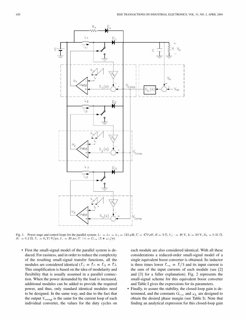
This section presents a summarized review of the control de-sign of parallel systems by means of small-signal models. Fig. 1shows the power stage and control loops for this system partic-ularised for three boost converter modules. For the sake of sim-plicity, and without an essential loss of generality, losses relatedto semiconductors, capacitors, and inductors are neglected. Thediode and the resistance are not considered in the analysissince they only work in the startup. The function repre-sents the proportional–integral compensator and stands forthe gain of the current-sensing network.
Linear control techniques have been extensively applied todesign the function , as it is described in [2]–[4]. Let usbriefly sum up the main steps involved in this design.
0278-0046/04$20.00 © 2004 IEEE
420 IEEE TRANSACTIONS ON INDUSTRIAL ELECTRONICS, VOL. 51, NO. 2, APRIL 2004
Fig. 1. Power stage and control loops for the parallel system: L = L = L = 123 �H, C = 470 �F, R = 9 , V = 48 V, E = 24 V, R = 0:31 ,R = 0:2 , S = 0; 15 V=�s, T = 20 �s, G (s) = G (1 + ! =s).
• First the small-signal model of the parallel system is de-duced. For easiness, and in order to reduce the complexityof the resulting small-signal transfer functions, all themodules are considered identical ( ).This simplification is based on the idea of modularity andflexibility that is usually assumed in a parallel connec-tion. When the power demanded by the load is increased,additional modules can be added to provide the requiredpower, and thus, only standard identical modules needto be designed. In the same way, and due to the fact thatthe output is the same for the current loop of eachindividual converter, the values for the duty cycles on
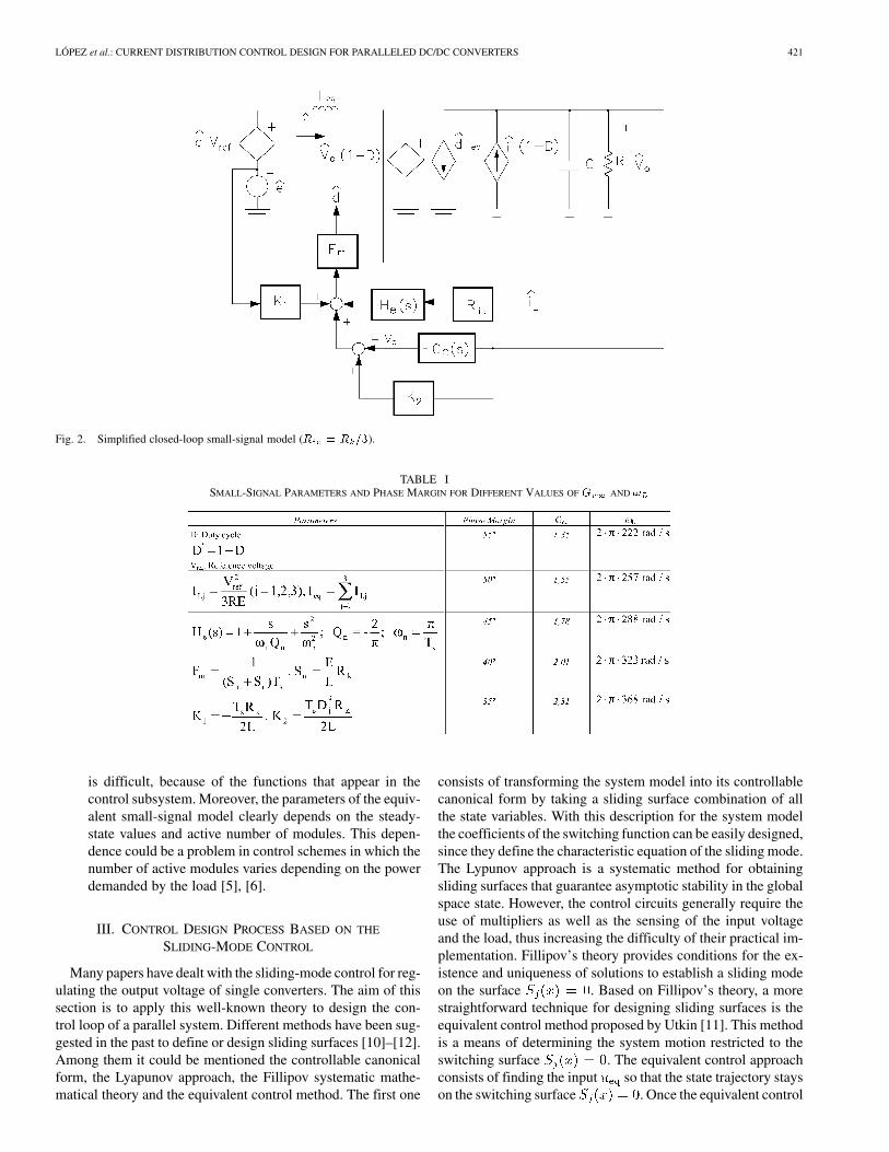
each module are also considered identical. With all theseconsiderations a reduced-order small-signal model of asingle equivalent boost converter is obtained. Its inductoris three times lower and its input current isthe sum of the input currents of each module (see [2]and [3] for a fuller explanation). Fig. 2 represents thesmall-signal scheme for this equivalent boost converterand Table I gives the expressions for its parameters.
• Finally, to assure the stability, the closed-loop gain is de-termined, and the constants and are designed toobtain the desired phase margin (see Table I). Note thatfinding an analytical expression for this closed-loop gain
LÓPEZ et al.: CURRENT DISTRIBUTION CONTROL DESIGN FOR PARALLELED DC/DC CONVERTERS 421
Fig. 2. Simplified closed-loop small-signal model (R = R =3).
TABLE ISMALL-SIGNAL PARAMETERS AND PHASE MARGIN FOR DIFFERENT VALUES OF G AND !
is difficult, because of the functions that appear in thecontrol subsystem. Moreover, the parameters of the equiv-alent small-signal model clearly depends on the steady-state values and active number of modules. This depen-dence could be a problem in control schemes in which thenumber of active modules varies depending on the powerdemanded by the load [5], [6].
III. CONTROL DESIGN PROCESS BASED ON THE
SLIDING-MODE CONTROL
Many papers have dealt with the sliding-mode control for reg-ulating the output voltage of single converters. The aim of thissection is to apply this well-known theory to design the con-trol loop of a parallel system. Different methods have been sug-gested in the past to define or design sliding surfaces [10]–[12].Among them it could be mentioned the controllable canonicalform, the Lyapunov approach, the Fillipov systematic mathe-matical theory and the equivalent control method. The first one
consists of transforming the system model into its controllablecanonical form by taking a sliding surface combination of allthe state variables. With this description for the system modelthe coefficients of the switching function can be easily designed,since they define the characteristic equation of the sliding mode.The Lypunov approach is a systematic method for obtainingsliding surfaces that guarantee asymptotic stability in the globalspace state. However, the control circuits generally require theuse of multipliers as well as the sensing of the input voltageand the load, thus increasing the difficulty of their practical im-plementation. Fillipov’s theory provides conditions for the ex-istence and uniqueness of solutions to establish a sliding modeon the surface . Based on Fillipov’s theory, a morestraightforward technique for designing sliding surfaces is theequivalent control method proposed by Utkin [11]. This methodis a means of determining the system motion restricted to theswitching surface . The equivalent control approachconsists of finding the input so that the state trajectory stayson the switching surface . Once the equivalent control
422 IEEE TRANSACTIONS ON INDUSTRIAL ELECTRONICS, VOL. 51, NO. 2, APRIL 2004
is known, the ideal sliding motion can be found by substitutingin the state equation and that the compensator designed to
obtain the desired response.This section is organized as follows. First the bilinear model,
the switching surfaces and their corresponding control laws arepresented. Second, based on the Utkin theory, conditions forthe existence of a sliding mode are found, and finally, with thementioned above equivalent control approach the equations ofthe motion are obtained and the controller is designed.
A. State Model and Sliding Surfaces
Let us consider again the parallel structure presented in Fig. 1.Conversely to the process based on small-signal models, themodules need not be identical and no design simplifications areassumed. Furthermore, the sliding-mode existence conditionsare found by considering a general case of boost converters.The inductor of each converter is denoted as ( ).The dynamical behavior of this system can be represented bythe state equations
(1)
The control input ( ) takes discrete valuesand , according to the control law that assigns its valuedepending on the sign of the switching surface
forfor
(2)
Likewise, the sliding surface for module can be identified withthe input signal in the block as
(3.a)
Note how once the state trajectory slides on the surface( , ), proper control actions lead toan equalization of the currents supplied by each converter,obtaining
(3.b)
The analysis of a variable-structure system is based on the as-sumption of infinitely high switching frequency. However inpractical power converters semiconductor switches have finiteswitching time, power losses increase with the switching fre-quency as well as parasitic elements take relevance in reactivecomponents. Therefore, the switching frequency has to be lim-ited or fixed to a constant value. The control scheme presented
in Fig. 1 works with a constant frequency [8], [9]. To achieve itthe control law (2) is implemented by comparing the switchingsurface with a ramp signal, which makes a function similar topulsewidth modulation (PWM). The frequency is assumed to behigh compared with the dynamics response of the system. Thus,the state trajectory evolves approximately like in the ideal caseand the design is made by applying the classical sliding-modeprocedure. As it is shown in [8], to avoid undesirable limit cyclebehavior the positive slope of ( ) must be lowerthan the slope of the ramp signal . By taking inexpression (3.a) its time derivative and replacing after (1) in theresult, it implies in the worst case ( , and ),satisfying the following inequality in steady state:
(4)
B. Sliding-Mode Existence Conditions
The model described by the state equations of (1) can be rep-resented by
(5)
where is the state vector, and , are vector fields. From Utkin theory we know that a sliding mode exists
in the vicinity of a switching surface if the following inequalitiesare satisfied [11], [12]:
(6.a)
(6.b)
Notation denotes the standard scalar product of and ,and corresponds to the gradient of . The design forthe sliding surface considering (6) is as follows.
1) If then according to the control law given in(2) . Applying (6.a) yields
(7.a)
where and . Noticethat the worst case in the inequality (7.a) corresponds to
( , ) that can be rewrittenconsidering and
as
(7.b)
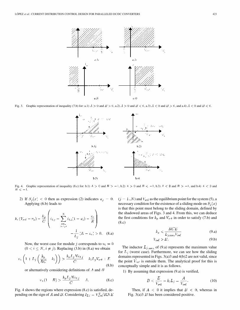
Thus, (7.b) can be graphically represented by Fig. 3.
LÓPEZ et al.: CURRENT DISTRIBUTION CONTROL DESIGN FOR PARALLELED DC/DC CONVERTERS 423
Fig. 3. Graphic representation of inequality (7.b) for: a.1) A > 0 and B > 0, a.2) A > 0 and B < 0, a.3) A < 0 and B > 0, and a.4) A < 0 and B < 0.
Fig. 4. Graphic representation of inequality (8.c) for: b.1) A > 0 and B > �1, b.2) A > 0 and B < �1, b.3) A < 0 and B > �1, and b.4) A < 0 andB < �1.
2) If then as expression (2) indicates .Applying (6.b) leads to
(8.a)
Now, the worst case for module corresponds to( , ). Replacing (3.b) in (8.a) we obtain
(8.b)or alternatively considering definitions of and
(8.c)
Fig. 4 shows the regions where expression (8.c) is satisfied, de-pending on the sign of and . Considering
( ) and as the equilibrium point for the system (5), anecessary condition for the existence of a sliding mode onis that this point must belong to the sliding domain, defined bythe shadowed areas of Figs. 3 and 4. From this, we can deducethe first conditions for and in order to satisfy (7.b) and(8.c)
(9.a)
(9.b)
The inductor of (9.a) represents the maximum valuefor (worst case). Furthermore, we can see how the slidingdomains represented in Figs. 3(a)3 and 4(b)2 are not valid, sincethe point is outside them. The analytical proof for this isconceptually simple and it is as follows.
1) By assuming that expression (9.a) is verified,
(10)
Then, if it implies that , whereas inFig. 3(a)3 has been considered positive.
424 IEEE TRANSACTIONS ON INDUSTRIAL ELECTRONICS, VOL. 51, NO. 2, APRIL 2004
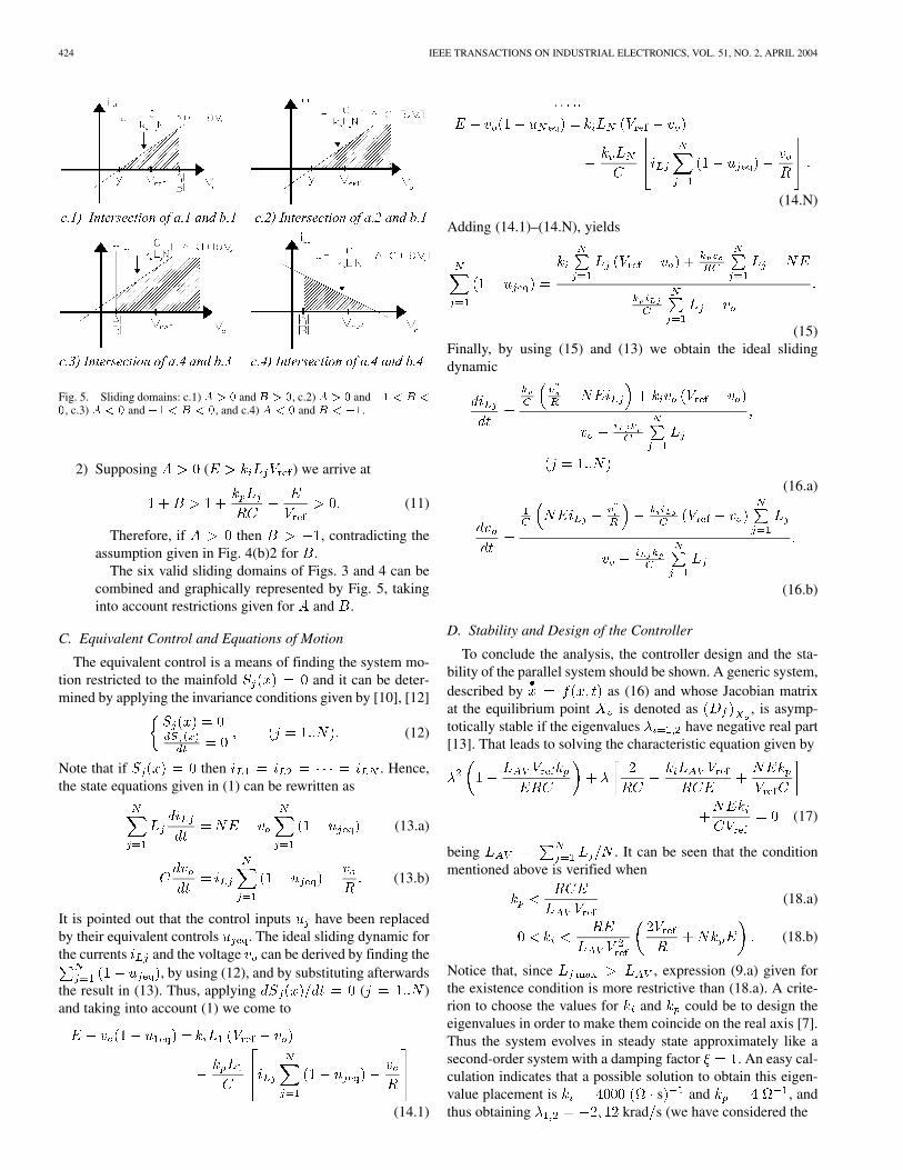
Fig. 5. Sliding domains: c.1)A > 0 andB > 0, c.2)A > 0 and�1 < B <0, c.3) A < 0 and �1 < B < 0, and c.4) A < 0 and B < �1.
2) Supposing ( ) we arrive at
(11)
Therefore, if then , contradicting theassumption given in Fig. 4(b)2 for .
The six valid sliding domains of Figs. 3 and 4 can becombined and graphically represented by Fig. 5, takinginto account restrictions given for and .
C. Equivalent Control and Equations of Motion
The equivalent control is a means of finding the system mo-tion restricted to the mainfold and it can be deter-mined by applying the invariance conditions given by [10], [12]
(12)
Note that if then . Hence,the state equations given in (1) can be rewritten as
(13.a)
(13.b)
It is pointed out that the control inputs have been replacedby their equivalent controls . The ideal sliding dynamic forthe currents and the voltage can be derived by finding the
, by using (12), and by substituting afterwardsthe result in (13). Thus, applying ( )and taking into account (1) we come to
(14.1)
(14.N)
Adding (14.1)–(14.N), yields
(15)Finally, by using (15) and (13) we obtain the ideal slidingdynamic
(16.a)
(16.b)
D. Stability and Design of the Controller
To conclude the analysis, the controller design and the sta-bility of the parallel system should be shown. A generic system,described by as (16) and whose Jacobian matrixat the equilibrium point is denoted as , is asymp-totically stable if the eigenvalues have negative real part[13]. That leads to solving the characteristic equation given by
(17)
being . It can be seen that the conditionmentioned above is verified when
(18.a)
(18.b)
Notice that, since , expression (9.a) given forthe existence condition is more restrictive than (18.a). A crite-rion to choose the values for and could be to design theeigenvalues in order to make them coincide on the real axis [7].Thus the system evolves in steady state approximately like asecond-order system with a damping factor . An easy cal-culation indicates that a possible solution to obtain this eigen-value placement is s and , andthus obtaining krad s (we have considered the
LÓPEZ et al.: CURRENT DISTRIBUTION CONTROL DESIGN FOR PARALLELED DC/DC CONVERTERS 425
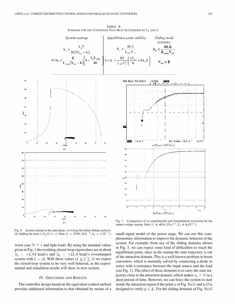
TABLE IISUMMARY FOR THE CONDITIONS THAT MUST BE SATISFIED BY k AND k
Fig. 6. System startup in the state plane. (a) Using the initial sliding surfaces.(b) Adding the term (�k R V ). Data: k = 1500 (s) , k = 2 ( ).
worst case and light load). By using the nominal valuesgiven in Fig. 1 the resulting closed-loop eigenvalues are at about
krad s and krad s (overdampedsystem with ). With these values ( ) we expectthe closed-loop system to be very well behaved, as the experi-mental and simulation results will show in next section.
IV. DISCUSSION AND RESULTS
The controller design based on the equivalent control methodprovides additional information to that obtained by means of a
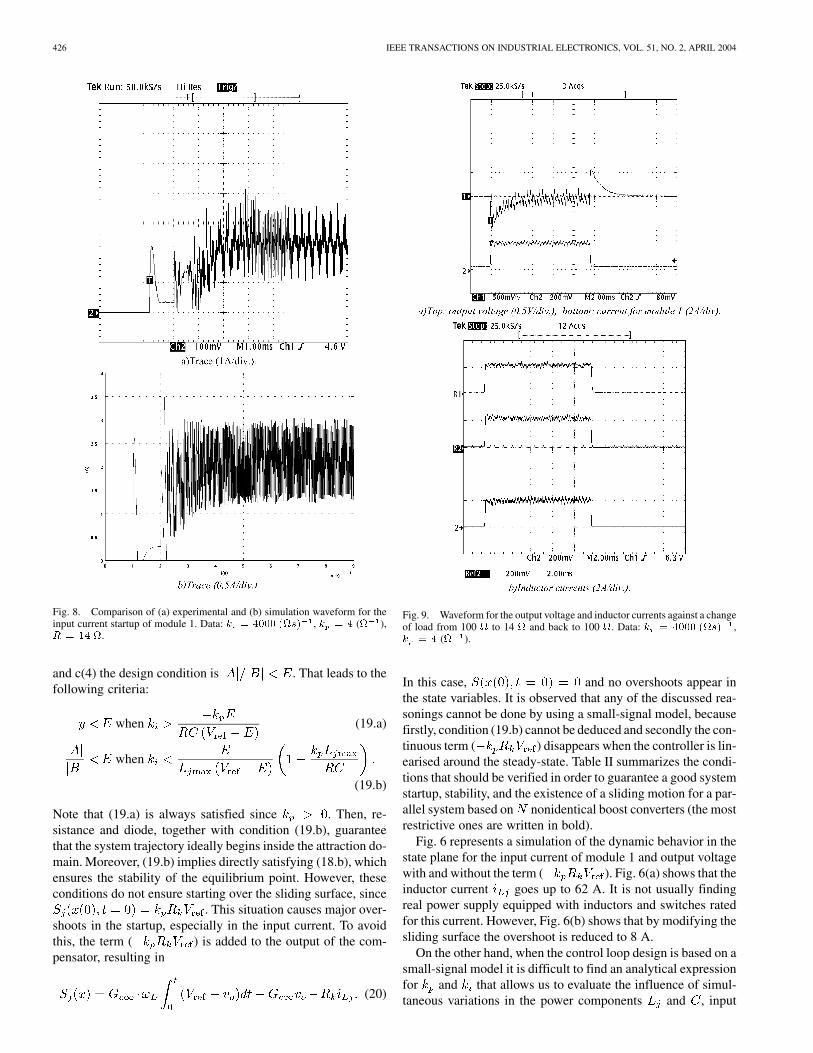
Fig. 7. Comparison of (a) experimental and (b)simulation waveform for theoutput voltage startup. Data: k = 4000 (s) , k = 4 ( ).
small-signal model of the power stage. We can use this com-plementary information to improve the dynamic behavior of thesystem. For example, from any of the sliding domains shownin Fig. 5, we can expect some kind of difficulties to reach theequilibrium point, since in the startup the state trajectory is outof the attraction domain. This is a well-known problem in boostconverters, which is normally solved by connecting a diode inseries with a resistance between the input source and the load(see Fig. 1). The effect of these elements is to carry the state tra-jectory close to the attraction domain, which makes in ashort period of time. However, we can force the system to startinside the attraction region if the point of Fig. 5(c)1 and (c)2 isdesigned to verify . For the sliding domains of Fig. 5(c)3
426 IEEE TRANSACTIONS ON INDUSTRIAL ELECTRONICS, VOL. 51, NO. 2, APRIL 2004
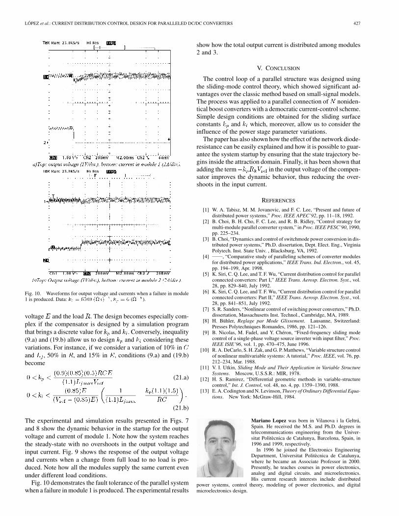
Fig. 8. Comparison of (a) experimental and (b) simulation waveform for theinput current startup of module 1. Data: k = 4000 (s) , k = 4 ( ),R = 14 .
and c(4) the design condition is . That leads to thefollowing criteria:
when (19.a)
when
(19.b)
Note that (19.a) is always satisfied since . Then, re-sistance and diode, together with condition (19.b), guaranteethat the system trajectory ideally begins inside the attraction do-main. Moreover, (19.b) implies directly satisfying (18.b), whichensures the stability of the equilibrium point. However, theseconditions do not ensure starting over the sliding surface, since
. This situation causes major over-shoots in the startup, especially in the input current. To avoidthis, the term ( ) is added to the output of the com-pensator, resulting in
(20)
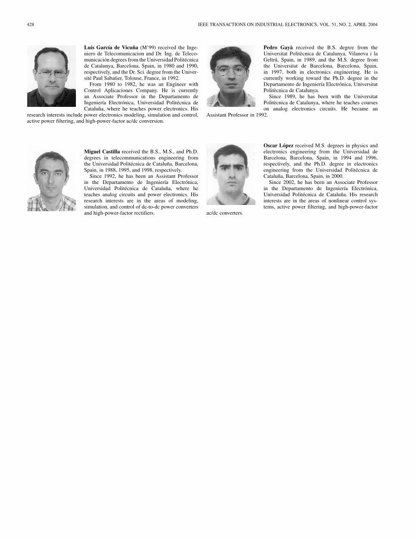
Fig. 9. Waveform for the output voltage and inductor currents against a changeof load from 100 to 14 and back to 100 . Data: k = 4000 (s) ,k = 4 ( ).
In this case, and no overshoots appear inthe state variables. It is observed that any of the discussed rea-sonings cannot be done by using a small-signal model, becausefirstly, condition (19.b) cannot be deduced and secondly the con-tinuous term ( ) disappears when the controller is lin-earised around the steady-state. Table II summarizes the condi-tions that should be verified in order to guarantee a good systemstartup, stability, and the existence of a sliding motion for a par-allel system based on nonidentical boost converters (the mostrestrictive ones are written in bold).
Fig. 6 represents a simulation of the dynamic behavior in thestate plane for the input current of module 1 and output voltagewith and without the term ( ). Fig. 6(a) shows that theinductor current goes up to 62 A. It is not usually findingreal power supply equipped with inductors and switches ratedfor this current. However, Fig. 6(b) shows that by modifying thesliding surface the overshoot is reduced to 8 A.
On the other hand, when the control loop design is based on asmall-signal model it is difficult to find an analytical expressionfor and that allows us to evaluate the influence of simul-taneous variations in the power components and , input
LÓPEZ et al.: CURRENT DISTRIBUTION CONTROL DESIGN FOR PARALLELED DC/DC CONVERTERS 427
Fig. 10. Waveforms for output voltage and currents when a failure in module1 is produced. Data: k = 6500 (s) , k = 6 ( ).
voltage and the load . The design becomes especially com-plex if the compensator is designed by a simulation programthat brings a discrete value for and . Conversely, inequality(9.a) and (19.b) allow us to design and considering thesevariations. For instance, if we consider a variation of 10% inand , 50% in , and 15% in , conditions (9.a) and (19.b)become
(21.a)
(21.b)
The experimental and simulation results presented in Figs. 7and 8 show the dynamic behavior in the startup for the outputvoltage and current of module 1. Note how the system reachesthe steady-state with no overshoots in the output voltage andinput current. Fig. 9 shows the response of the output voltageand currents when a change from full load to no load is pro-duced. Note how all the modules supply the same current evenunder different load conditions.
Fig. 10 demonstrates the fault tolerance of the parallel systemwhen a failure in module 1 is produced. The experimental results
show how the total output current is distributed among modules2 and 3.
V. CONCLUSION
The control loop of a parallel structure was designed usingthe sliding-mode control theory, which showed significant ad-vantages over the classic method based on small-signal models.The process was applied to a parallel connection of noniden-tical boost converters with a democratic current-control scheme.Simple design conditions are obtained for the sliding surfaceconstants and which, moreover, allow us to consider theinfluence of the power stage parameter variations.
The paper has also shown how the effect of the network diode-resistance can be easily explained and how it is possible to guar-antee the system startup by ensuring that the state trajectory be-gins inside the attraction domain. Finally, it has been shown thatadding the term in the output voltage of the compen-sator improves the dynamic behavior, thus reducing the over-shoots in the input current.
REFERENCES
[1] W. A. Tabisz, M. M. Jovanovic, and F. C. Lee, “Present and future ofdistributed power systems,” Proc. IEEE APEC’92, pp. 11–18, 1992.
[2] B. Choi, B. H. Cho, F. C. Lee, and R. B. Ridley, “Control strategy formulti-module parallel converter system,” in Proc. IEEE PESC’90, 1990,pp. 225–234.
[3] B. Choi, “Dynamics and control of switchmode power conversion in dis-tributed power systems,” Ph.D. dissertation, Dept. Elect. Eng., VirginiaPolytech. Inst. State Univ. , Blacksburg, VA, 1992.
[4] , “Comparative study of paralleling schemes of converter modulesfor distributed power applications,” IEEE Trans. Ind. Electron., vol. 45,pp. 194–199, Apr. 1998.
[5] K. Siri, C. Q. Lee, and T. F. Wu, “Current distribution control for parallelconnected converters: Part I,” IEEE Trans. Aerosp. Electron. Syst., vol.28, pp. 829–840, July 1992.
[6] K. Siri, C. Q. Lee, and T. F. Wu, “Current distribution control for parallelconnected converters: Part II,” IEEE Trans. Aerosp. Electron. Syst., vol.28, pp. 841–851, July 1992.
[7] S. R. Sanders, “Nonlinear control of switching power converters,” Ph.D.dissertation, Massachusetts Inst. Technol., Cambridge, MA, 1989.
[8] H. Bühler, Reglage par Mode Glissement. Lausanne, Switzerland:Presses Polytechniques Romandes, 1986, pp. 121–126.
[9] B. Nicolas, M. Fadel, and Y. Chéron, “Fixed-frequency sliding modecontrol of a single-phase voltage source inverter with input filter,” Proc.IEEE ISIE’96, vol. 1, pp. 470–475, June 1996.
[10] R. A. DeCarlo, S. H. Zak, and G. P. Matthews, “Variable structure controlof nonlinear multivariable systems: A tutorial,” Proc. IEEE, vol. 76, pp.212–234, Mar. 1988.
[11] V. I. Utkin, Sliding Mode and Their Application in Variable StructureSystems. Moscow, U.S.S.R.: MIR, 1978.
[12] H. S. Ramirez, “Differential geometric methods in variable-structurecontrol,” Int. J. Control, vol. 48, no. 4, pp. 1359–1390, 1988.
[13] E. A. Codington and N. Levinson, Theory of Ordinary Differential Equa-tions. New York: McGraw-Hill, 1984.
Mariano Lopez was born in Vilanova i la Geltrú,Spain. He received the M.S. and Ph.D. degrees intelecommunications engineering from the Univer-sitat Politècnica de Catalunya, Barcelona, Spain, in1996 and 1999, respectively.
In 1996 he joined the Electronics EngineeringDepartment, Universitat Politècnica de Catalunya,where he became an Associate Professor in 2000.Presently, he teaches courses in power electronics,analog and digital circuits. and microelectronics.His current research interests include distributed
power systems, control theory, modeling of power electronics, and digitalmicroelectronics design.
428 IEEE TRANSACTIONS ON INDUSTRIAL ELECTRONICS, VOL. 51, NO. 2, APRIL 2004
Luis García de Vicuña (M’99) received the Inge-niero de Telecomunicacion and Dr. Ing. de Teleco-municación degrees from the Universidad Politécnicade Catalunya, Barcelona, Spain, in 1980 and 1990,respectively, and the Dr. Sci. degree from the Univer-sité Paul Sabatier, Tolouse, France, in 1992.
From 1980 to 1982, he was an Engineer withControl Aplicaciones Company. He is currentlyan Associate Professor in the Departamento deIngeniería Electrónica, Universidad Politécnica deCataluña, where he teaches power electronics. His
research interests include power electronics modeling, simulation and control,active power filtering, and high-power-factor ac/dc conversion.
Miguel Castilla received the B.S., M.S., and Ph.D.degrees in telecommunications engineering fromthe Universidad Politécnica de Cataluña, Barcelona,Spain, in 1988, 1995, and 1998, respectively.
Since 1992, he has been an Assistant Professorin the Departamento de Ingeniería Electrónica,Universidad Politécnica de Cataluña, where heteaches analog circuits and power electronics. Hisresearch interests are in the areas of modeling,simulation, and control of dc-to-dc power convertersand high-power-factor rectifiers.
Pedro Gayà received the B.S. degree from theUniversitat Politècnica de Catalunya, Vilanova i laGeltrú, Spain, in 1989, and the M.S. degree fromthe Universitat de Barcelona, Barcelona, Spain,in 1997, both in electronics engineering. He iscurrently working toward the Ph.D. degree in theDepartamento de Ingeniería Electrónica, UniversitatPolitècnica de Catalunya.
Since 1989, he has been with the UniversitatPolitècnica de Catalunya, where he teaches courseson analog electronics circuits. He became an
Assistant Professor in 1992.
Oscar López received M.S. degrees in physics andelectronics engineering from the Universidad deBarcelona, Barcelona, Spain, in 1994 and 1996,respectively, and the Ph.D. degree in electronicsengineering from the Universidad Politécnica deCataluña, Barcelona, Spain, in 2000.
Since 2002, he has been an Associate Professorin the Departamento de Ingeniería Electrónica,Universidad Politécnica de Cataluña. His researchinterests are in the areas of nonlinear control sys-tems, active power filtering, and high-power-factor
ac/dc converters.
Related Documents