CSE477 L04 CMOS Inverter.1 Irwin&Vijay, PSU, 2002 ECE484 VLSI Digital Circuits Fall 2010 Lecture 04: CMOS Inverter (static view) Mary Jane Irwin ( www.cse.psu.edu/~mji ) www.cse.psu.edu/~cg477 Modified by Dr. George Engel (SIUE) [Adapted from Rabaey’s Digital Integrated Circuits, ©2002, J. Rabaey et al.]

CSE477 L04 CMOS Inverter.1Irwin&Vijay, PSU, 2002 ECE484 VLSI Digital Circuits Fall 2010 Lecture 04: CMOS Inverter (static view) Mary Jane Irwin ( mji.
Dec 26, 2015
Welcome message from author
This document is posted to help you gain knowledge. Please leave a comment to let me know what you think about it! Share it to your friends and learn new things together.
Transcript
CSE477 L04 CMOS Inverter.1 Irwin&Vijay, PSU, 2002
ECE484VLSI Digital Circuits
Fall 2010
Lecture 04: CMOS Inverter (static view)
Mary Jane Irwin ( www.cse.psu.edu/~mji ) www.cse.psu.edu/~cg477
Modified by Dr. George Engel (SIUE)
[Adapted from Rabaey’s Digital Integrated Circuits, ©2002, J. Rabaey et al.]
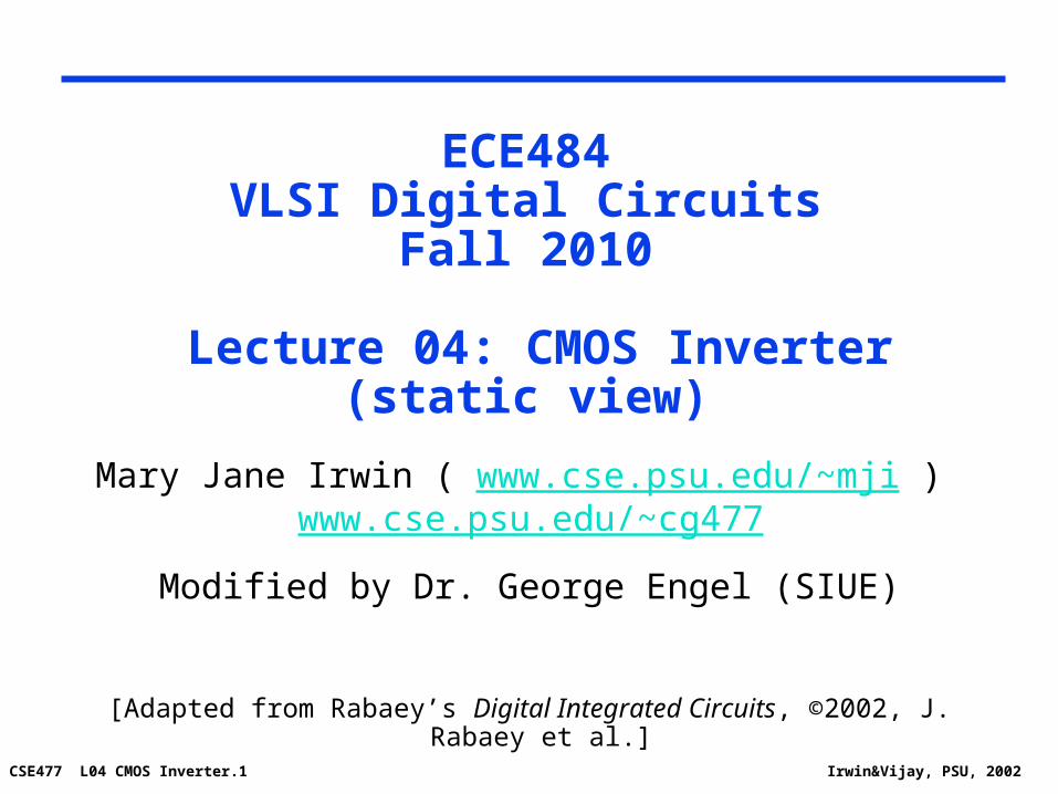
CSE477 L04 CMOS Inverter.2 Irwin&Vijay, PSU, 2002
CMOS Inverter: A First Look
VDD
Vout
CL
Vin

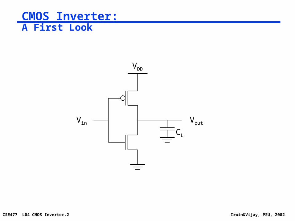
CSE477 L04 CMOS Inverter.3 Irwin&Vijay, PSU, 2002
CMOS Inverter: Steady State Response
VDD
Rn
Vout = 0
Vin = V DD
VDD
Rp
Vout = 1
Vin = 0
VOL = 0VOH = VDD
VM = f(Rn, Rp)
CSE477 L04 CMOS Inverter.4 Irwin&Vijay, PSU, 2002
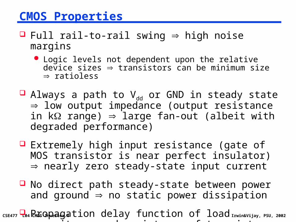
CMOS Properties
Full rail-to-rail swing high noise margins Logic levels not dependent upon the relative device sizes
transistors can be minimum size ratioless
Always a path to Vdd or GND in steady state low output impedance (output resistance in k range) large fan-out (albeit with degraded performance)
Extremely high input resistance (gate of MOS transistor is near perfect insulator) nearly zero steady-state input current
No direct path steady-state between power and ground no static power dissipation
Propagation delay function of load capacitance and resistance of transistors

CSE477 L04 CMOS Inverter.5 Irwin&Vijay, PSU, 2002
Review: Short Channel I-V Plot (NMOS)
0
0.5
1
1.5
2
2.5
0 0.5 1 1.5 2 2.5
I D (
A)
VDS (V)
X 10-4
VGS = 1.0V
VGS = 1.5V
VGS = 2.0V
VGS = 2.5V
Lin
ear
de
pe
nde
nce
NMOS transistor, 0.25um, Ld = 0.25um, W/L = 1.5, VDD = 2.5V, VT = 0.4V

CSE477 L04 CMOS Inverter.6 Irwin&Vijay, PSU, 2002
Review: Short Channel I-V Plot (PMOS)
-1
-0.8
-0.6
-0.4
-0.2
00-1-2
I D (
A)
VDS (V)
X 10-4
VGS = -1.0V
VGS = -1.5V
VGS = -2.0V
VGS = -2.5V
PMOS transistor, 0.25um, Ld = 0.25um, W/L = 1.5, VDD = 2.5V, VT = -0.4V
All polarities of all voltages and currents are reversed
CSE477 L04 CMOS Inverter.7 Irwin&Vijay, PSU, 2002
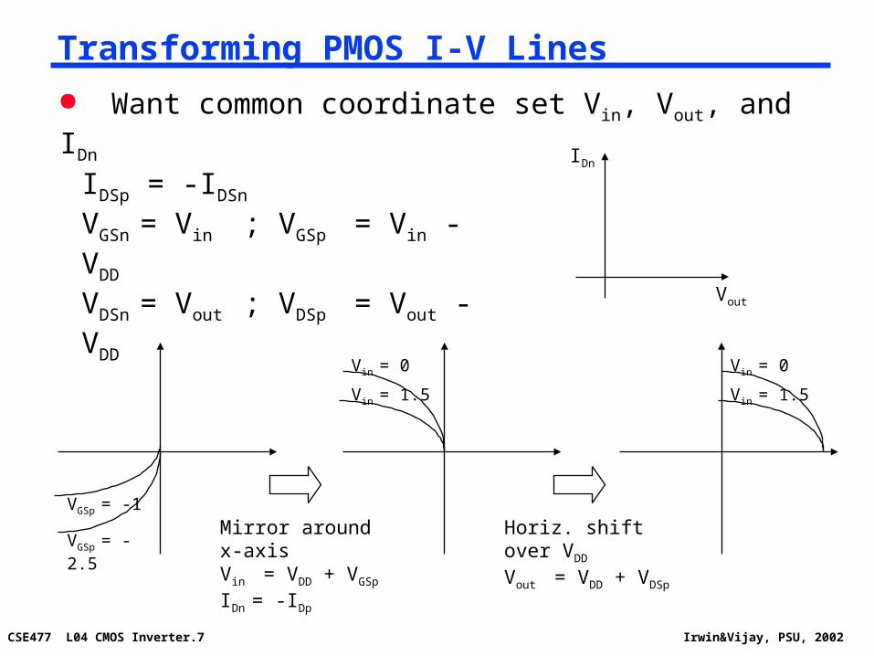
Transforming PMOS I-V Lines
IDSp = -IDSn
VGSn = Vin ; VGSp = Vin - VDD
VDSn = Vout ; VDSp = Vout - VDDVout
IDn
VGSp = -2.5
VGSp = -1
Mirror around x-axisVin = VDD + VGSp
IDn = -IDp
Vin = 1.5
Vin = 0
Vin = 1.5
Vin = 0
Horiz. shift over VDD
Vout = VDD + VDSp
Want common coordinate set Vin, Vout, and IDn
CSE477 L04 CMOS Inverter.8 Irwin&Vijay, PSU, 2002
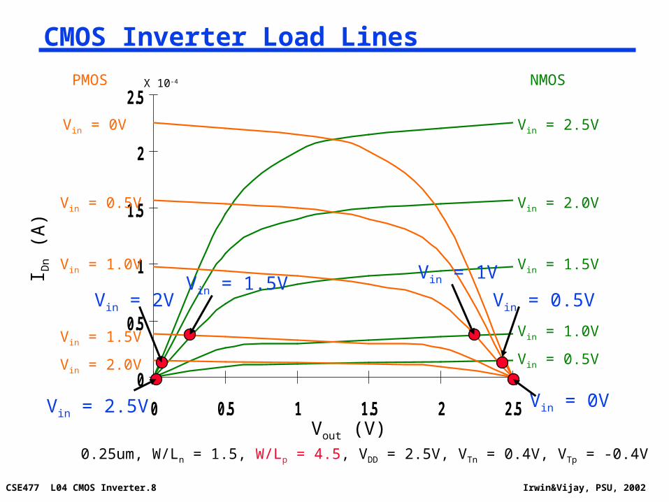
CMOS Inverter Load Lines
0
0.5
1
1.5
2
2.5
0 0.5 1 1.5 2 2.5
I Dn (
A)
Vout (V)
X 10-4
Vin = 1.0V
Vin = 1.5V
Vin = 2.0V
Vin = 2.5V
0.25um, W/Ln = 1.5, W/Lp = 4.5, VDD = 2.5V, VTn = 0.4V, VTp = -0.4V
Vin = 0V
Vin = 0.5V
Vin = 1.0V
Vin = 1.5V
Vin = 0.5VVin = 2.0V
Vin = 2.5V
Vin = 2VVin = 1.5V
Vin = 1V
Vin = 0.5V
Vin = 0V
PMOS NMOS

CSE477 L04 CMOS Inverter.10 Irwin&Vijay, PSU, 2002
CMOS Inverter VTC
0
0.5
1
1.5
2
2.5
0 0.5 1 1.5 2 2.5
Vin (V)
Vo
ut (
V)
NMOS offPMOS res
NMOS satPMOS res
NMOS satPMOS sat
NMOS resPMOS sat NMOS res
PMOS off

CSE477 L04 CMOS Inverter.12 Irwin&Vijay, PSU, 2002
CMOS Inverter: Switch Model of Dynamic Behavior
VDD
Rn
Vout
CL
Vin = V DD
VDD
Rp
Vout
CL
Vin = 0
Gate response time is determined by the time to charge CL through Rp (discharge CL through Rn)

CSE477 L04 CMOS Inverter.13 Irwin&Vijay, PSU, 2002
Relative Transistor Sizing
When designing static CMOS circuits, balance the driving strengths of the transistors by making the PMOS section wider than the NMOS section to
maximize the noise margins and obtain symmetrical characteristics

CSE477 L04 CMOS Inverter.14 Irwin&Vijay, PSU, 2002
Switching Threshold
VM where Vin = Vout (both PMOS and NMOS in saturation since VDS = VGS)
VM rVDD/(1 + r) where r = kpVDSATp/knVDSATn
Switching threshold set by the ratio r, which compares the relative driving strengths of the PMOS and NMOS transistors
Want VM = VDD/2 (to have comparable high and low noise margins), so want r 1
(W/L)p kn’VDSATn(VM-VTn-VDSATn/2)
(W/L)n kp’VDSATp(VDD-VM+VTp+VDSATp/2)
=
CSE477 L04 CMOS Inverter.16 Irwin&Vijay, PSU, 2002
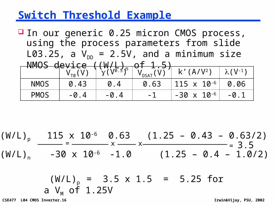
Switch Threshold Example
In our generic 0.25 micron CMOS process, using the process parameters from slide L03.25, a VDD = 2.5V, and a minimum size NMOS device ((W/L)n of 1.5)
VT0(V) (V0.5) VDSAT(V) k’(A/V2) (V-1)
NMOS 0.43 0.4 0.63 115 x 10-6 0.06
PMOS -0.4 -0.4 -1 -30 x 10-6 -0.1
(W/L)p 115 x 10-6 0.63 (1.25 – 0.43 – 0.63/2)
(W/L)n -30 x 10-6 -1.0 (1.25 – 0.4 – 1.0/2)= x x = 3.5
(W/L)p = 3.5 x 1.5 = 5.25 for a VM of 1.25V
CSE477 L04 CMOS Inverter.17 Irwin&Vijay, PSU, 2002
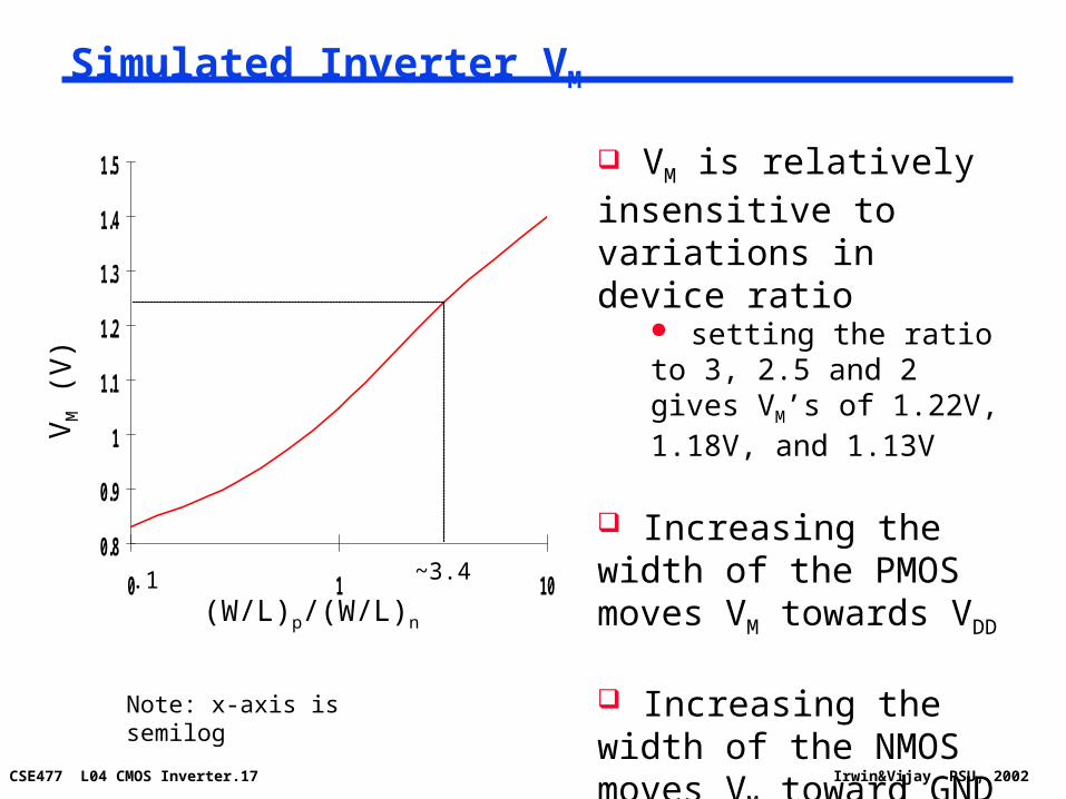
Simulated Inverter VM
0.8
0.9
1
1.1
1.2
1.3
1.4
1.5
0 1 10(W/L)p/(W/L)n
VM (
V)
VM is relatively insensitive to variations in device ratio
setting the ratio to 3, 2.5 and 2 gives VM’s of 1.22V, 1.18V, and 1.13V
Increasing the width of the PMOS moves VM towards VDD
Increasing the width of the NMOS moves VM toward GND
.1
Note: x-axis is semilog
~3.4

CSE477 L04 CMOS Inverter.18 Irwin&Vijay, PSU, 2002
Noise Margins Determining VIH and VIL
0
1
2
3
VIL VIHVin
Vo
ut
VOH = VDD
VM
By definition, VIH and VIL are where dVout/dVin = -1 (= gain)
VOL = GND
A piece-wise linear approximation of VTC
NMH = VDD - VIH
NML = VIL - GND
Approximating: VIH = VM - VM /g VIL = VM + (VDD - VM )/g
So high gain in the transition region is very desirable

CSE477 L04 CMOS Inverter.19 Irwin&Vijay, PSU, 2002
CMOS Inverter VTC from Simulation
0
0.5
1
1.5
2
2.5
0 0.5 1 1.5 2 2.5
Vin (V)
Vo
ut (
V)
0.25um, (W/L)p/(W/L)n = 3.4(W/L)n = 1.5 (min size)VDD = 2.5V
VM 1.25V, g = -27.5
VIL = 1.2V, VIH = 1.3VNML = NMH = 1.2(actual values are VIL = 1.03V, VIH = 1.45VNML = 1.03V & NMH = 1.05V)
Output resistance low-output = 2.4khigh-output = 3.3k

CSE477 L04 CMOS Inverter.20 Irwin&Vijay, PSU, 2002
Gain Determinates
-18
-16
-14
-12
-10
-8
-6
-4
-2
0
0 0.5 1 1.5 2
Vin
gai
n
Gain is a strong function of the slopes of the currents in the saturation region, for Vin = VM
(1+r)g ---------------------------------- (VM-VTn-VDSATn/2)(n - p )
Determined by technology parameters, especially channel length modulation (). Only designer influence through supply voltage and VM (transistor sizing).

CSE477 L04 CMOS Inverter.21 Irwin&Vijay, PSU, 2002
Impact of Process Variation on VTC Curve
0
0.5
1
1.5
2
2.5
0 0.5 1 1.5 2 2.5
Vin (V)
Vo
ut (
V)
Nominal
Good PMOSBad NMOS
Bad PMOSGood NMOS
Process variations (mostly) cause a shift in the switching threshold
CSE477 L04 CMOS Inverter.22 Irwin&Vijay, PSU, 2002
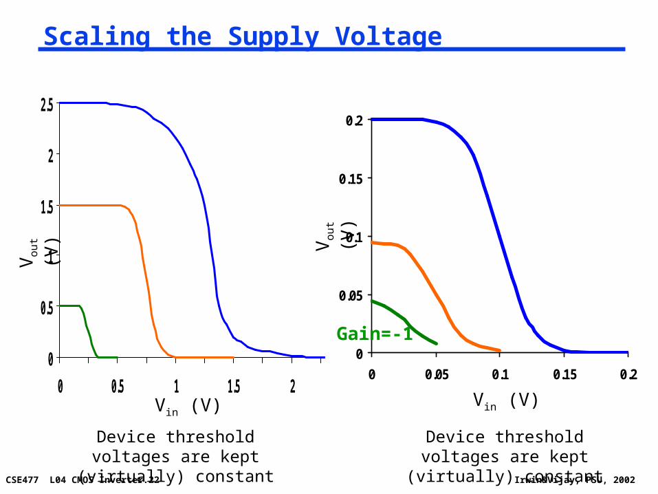
Scaling the Supply Voltage
0
0.5
1
1.5
2
2.5
0 0.5 1 1.5 2 2.5Vin (V)
Vo
ut (
V)
Device threshold voltages are kept (virtually) constant
0
0.05
0.1
0.15
0.2
0 0.05 0.1 0.15 0.2
Vin (V)
Vo
ut (
V)
Gain=-1
Device threshold voltages are kept (virtually) constant
Related Documents