CSE477 L02 Design Metrics.1 Irwin&Vijay, PSU, 2002 ECE 484 VLSI Digital Circuits Fall 2014 Lecture 02: Design Metrics Dr. George L. Engel Adapted from slides provided by Mary Jane Irwin (PSU) [Adapted from Rabaey’s Digital Integrated Circuits, ©2002, J. Rabaey et al.]

Welcome message from author
This document is posted to help you gain knowledge. Please leave a comment to let me know what you think about it! Share it to your friends and learn new things together.
Transcript
CSE477 L02 Design Metrics.1 Irwin&Vijay, PSU, 2002
ECE 484VLSI Digital Circuits
Fall 2014
Lecture 02: Design Metrics
Dr. George L. Engel
Adapted from slides provided by Mary Jane Irwin (PSU)
[Adapted from Rabaey’s Digital Integrated Circuits, ©2002, J. Rabaey et al.]
CSE477 L02 Design Metrics.2 Irwin&Vijay, PSU, 2002
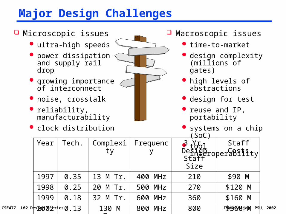
Major Design Challenges
Microscopic issues ultra-high speeds power dissipation and
supply rail drop growing importance of
interconnect noise, crosstalk reliability,
manufacturability clock distribution
Macroscopic issues time-to-market design complexity
(millions of gates) high levels of
abstractions design for test reuse and IP, portability systems on a chip (SoC) tool interoperability
Year Tech. Complexity Frequency 3 Yr. Design Staff Size
Staff Costs
1997 0.35 13 M Tr. 400 MHz 210 $90 M
1998 0.25 20 M Tr. 500 MHz 270 $120 M
1999 0.18 32 M Tr. 600 MHz 360 $160 M
2002 0.13 130 M Tr. 800 MHz 800 $360 M
CSE477 L02 Design Metrics.3 Irwin&Vijay, PSU, 2002
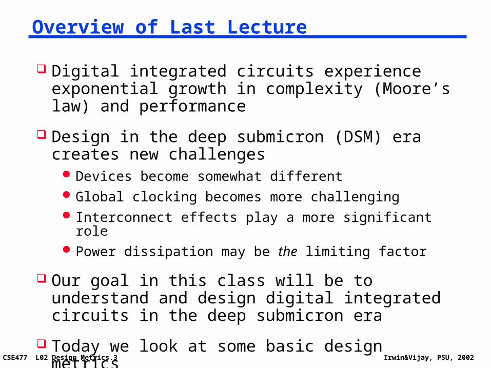
Overview of Last Lecture
Digital integrated circuits experience exponential growth in complexity (Moore’s law) and performance
Design in the deep submicron (DSM) era creates new challenges
Devices become somewhat different Global clocking becomes more challenging Interconnect effects play a more significant role Power dissipation may be the limiting factor
Our goal in this class will be to understand and design digital integrated circuits in the deep submicron era
Today we look at some basic design metrics

CSE477 L02 Design Metrics.4 Irwin&Vijay, PSU, 2002
Fundamental Design Metrics
Functionality
Cost NRE (fixed) costs - design effort RE (variable) costs - cost of parts, assembly, test
Reliability, robustness Noise margins Noise immunity
Performance Speed (delay) Power consumption; energy
Time-to-market
CSE477 L02 Design Metrics.5 Irwin&Vijay, PSU, 2002
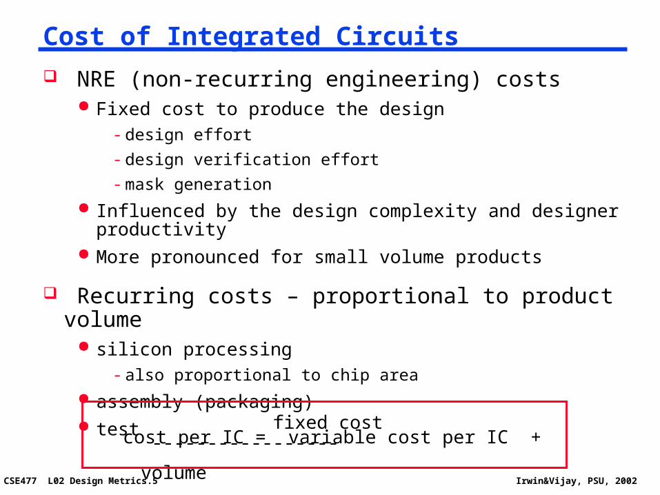
Cost of Integrated Circuits
NRE (non-recurring engineering) costs Fixed cost to produce the design
- design effort
- design verification effort
- mask generation
Influenced by the design complexity and designer productivity More pronounced for small volume products
Recurring costs – proportional to product volume silicon processing
- also proportional to chip area
assembly (packaging) test
fixed costcost per IC = variable cost per IC + -----------------
volume
CSE477 L02 Design Metrics.6 Irwin&Vijay, PSU, 2002
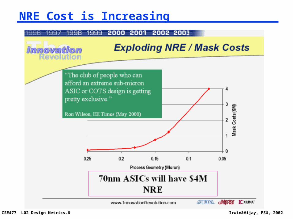
NRE Cost is Increasing

CSE477 L02 Design Metrics.7 Irwin&Vijay, PSU, 2002
Silicon Wafer
Single die
Wafer
From http://www.amd.com
CSE477 L02 Design Metrics.8 Irwin&Vijay, PSU, 2002
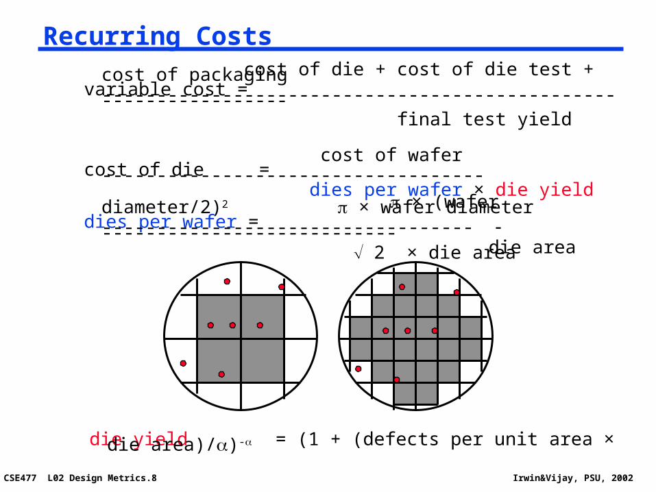
Recurring Costs cost of die + cost of die test + cost of packagingvariable cost = ----------------------------------------------------------------
final test yield
cost of wafercost of die = -----------------------------------
dies per wafer × die yield
× (wafer diameter/2)2 × wafer diameterdies per wafer = ---------------------------------- --------------------------- die area 2 × die area
die yield = (1 + (defects per unit area × die area)/)-
CSE477 L02 Design Metrics.9 Irwin&Vijay, PSU, 2002
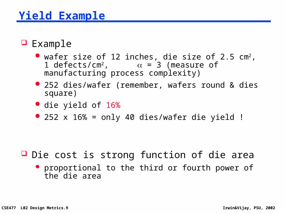
Yield Example
Example wafer size of 12 inches, die size of 2.5 cm2, 1 defects/cm2,
= 3 (measure of manufacturing process complexity) 252 dies/wafer (remember, wafers round & dies square) die yield of 16% 252 x 16% = only 40 dies/wafer die yield !
Die cost is strong function of die area proportional to the third or fourth power of the die area
CSE477 L02 Design Metrics.10 Irwin&Vijay, PSU, 2002
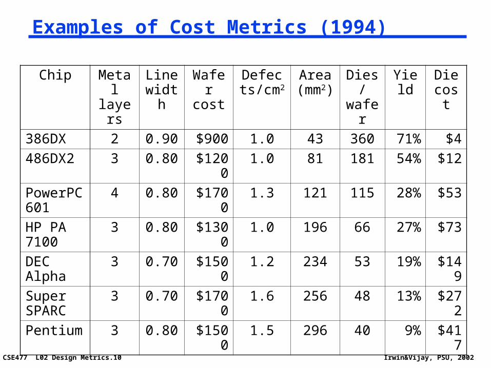
Examples of Cost Metrics (1994)
Chip Metal layers
Line width
Wafer cost
Defects/cm2
Area (mm2)
Dies/wafer
Yield Die cost
386DX 2 0.90 $900 1.0 43 360 71% $4
486DX2 3 0.80 $1200 1.0 81 181 54% $12
PowerPC 601
4 0.80 $1700 1.3 121 115 28% $53
HP PA 7100
3 0.80 $1300 1.0 196 66 27% $73
DEC Alpha
3 0.70 $1500 1.2 234 53 19% $149
Super SPARC
3 0.70 $1700 1.6 256 48 13% $272
Pentium 3 0.80 $1500 1.5 296 40 9% $417
CSE477 L02 Design Metrics.11 Irwin&Vijay, PSU, 2002
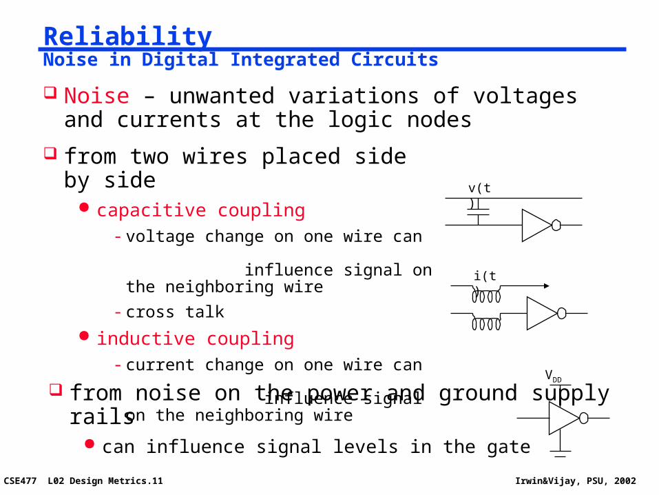
ReliabilityNoise in Digital Integrated Circuits
Noise – unwanted variations of voltages and currents at the logic nodes
VDD
v(t)
i(t)
from two wires placed side by side capacitive coupling
- voltage change on one wire can influence signal on the neighboring wire
- cross talk
inductive coupling- current change on one wire can
influence signal on the neighboring wire
from noise on the power and ground supply rails can influence signal levels in the gate
CSE477 L02 Design Metrics.12 Irwin&Vijay, PSU, 2002
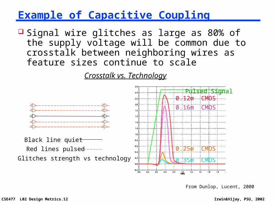
Example of Capacitive Coupling
Signal wire glitches as large as 80% of the supply voltage will be common due to crosstalk between neighboring wires as feature sizes continue to scale
Crosstalk vs. Technology
0.16m CMOS
0.12m CMOS
0.35m CMOS
0.25m CMOS
Pulsed Signal
Black line quiet
Red lines pulsed
Glitches strength vs technology
From Dunlop, Lucent, 2000
CSE477 L02 Design Metrics.13 Irwin&Vijay, PSU, 2002
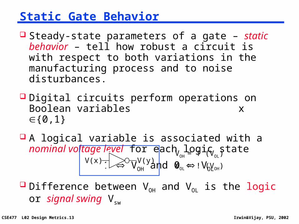
Static Gate Behavior
Steady-state parameters of a gate – static behavior – tell how robust a circuit is with respect to both variations in the manufacturing process and to noise disturbances.
Digital circuits perform operations on Boolean variables x {0,1}
A logical variable is associated with a nominal voltage level for each logic state
1 VOH and 0 VOL
Difference between VOH and VOL is the logic or signal swing Vsw
V(y)V(x)VOH = ! (VOL)
VOL = ! (VOH)
CSE477 L02 Design Metrics.14 Irwin&Vijay, PSU, 2002
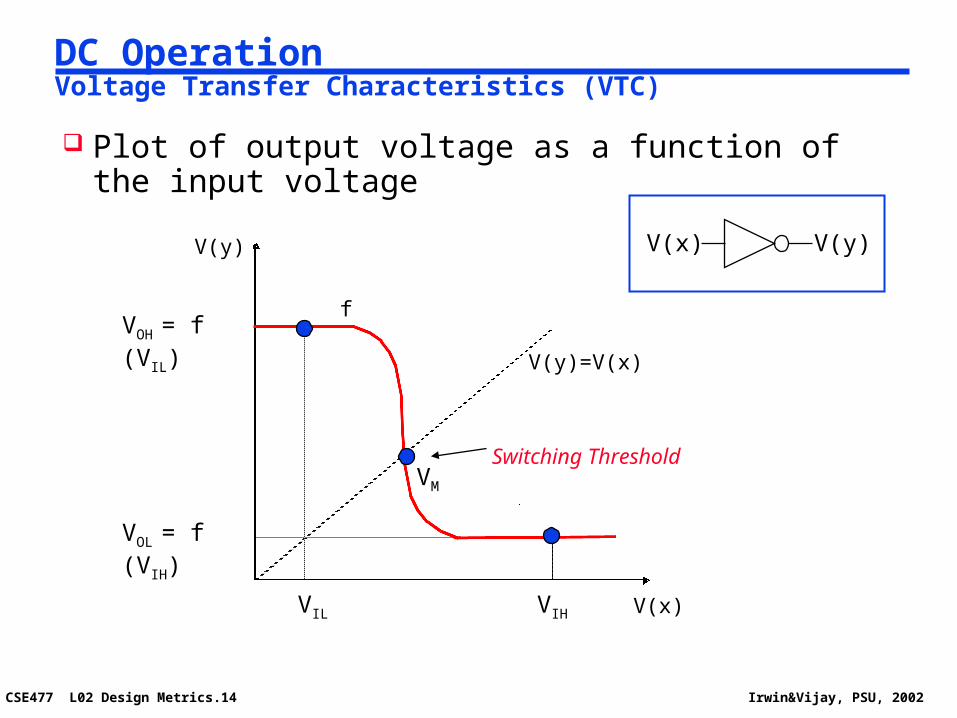
DC Operation Voltage Transfer Characteristics (VTC)
V(x)
V(y)
f
V(y)V(x)
Plot of output voltage as a function of the input voltage
VOH = f (VIL)
VIL VIH
V(y)=V(x)
Switching ThresholdVM
VOL = f (VIH)
CSE477 L02 Design Metrics.15 Irwin&Vijay, PSU, 2002
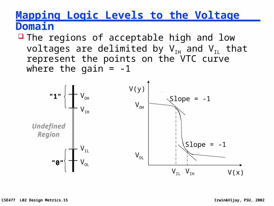
Mapping Logic Levels to the Voltage Domain
V(x)
V(y)
Slope = -1
Slope = -1
VOH
VOL
VIL VIH
"1"
"0"
UndefinedRegion
VOH
VOL
VIL
VIH
The regions of acceptable high and low voltages are delimited by VIH and VIL that represent the points on the VTC curve where the gain = -1
CSE477 L02 Design Metrics.16 Irwin&Vijay, PSU, 2002
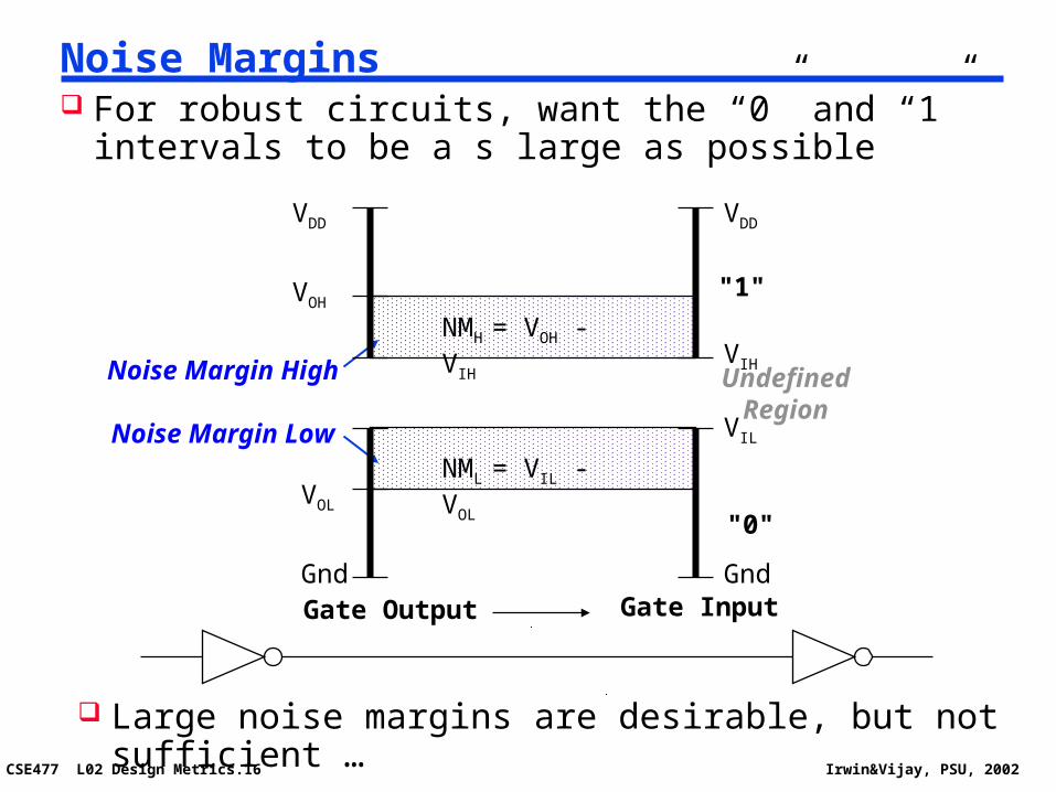
Noise Margins
UndefinedRegion
"1"
"0"
Gate Output Gate Input
VOH
VIL
VOL
VIHNoise Margin High
Noise Margin Low
NMH = VOH - VIH
NML = VIL - VOL
Large noise margins are desirable, but not sufficient …
Gnd
VDD VDD
Gnd
For robust circuits, want the “0” and “1” intervals to be a s large as possible
CSE477 L02 Design Metrics.17 Irwin&Vijay, PSU, 2002
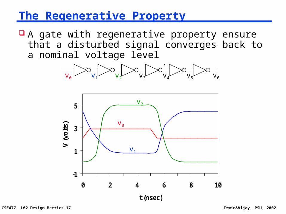
The Regenerative Property
v0 v1 v2 v3 v4 v5 v6
-1
1
3
5
0 2 4 6 8 10
t (nsec)
V (
volt
s) v0
v2
v1
A gate with regenerative property ensure that a disturbed signal converges back to a nominal voltage level
CSE477 L02 Design Metrics.18 Irwin&Vijay, PSU, 2002
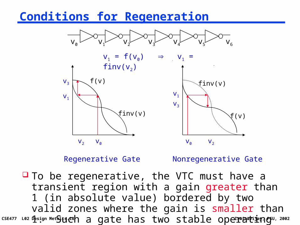
Conditions for Regeneration
v1 = f(v0) v1 = finv(v2)
v0 v1 v2 v3 v4 v5 v6
v0
v1
v2
v3 f(v)
finv(v)
Regenerative Gate
v0
v1
v2
v3
f(v)
finv(v)
Nonregenerative Gate
To be regenerative, the VTC must have a transient region with a gain greater than 1 (in absolute value) bordered by two valid zones where the gain is smaller than 1. Such a gate has two stable operating points.
CSE477 L02 Design Metrics.19 Irwin&Vijay, PSU, 2002
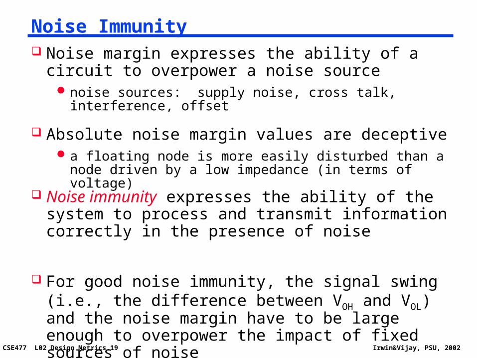
Noise Immunity
Noise immunity expresses the ability of the system to process and transmit information correctly in the presence of noise
For good noise immunity, the signal swing (i.e., the difference between VOH and VOL) and the noise margin have to be large enough to overpower the impact of fixed sources of noise
Noise margin expresses the ability of a circuit to overpower a noise source
noise sources: supply noise, cross talk, interference, offset
Absolute noise margin values are deceptive a floating node is more easily disturbed than a node driven by a
low impedance (in terms of voltage)
CSE477 L02 Design Metrics.20 Irwin&Vijay, PSU, 2002
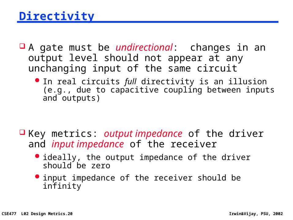
Directivity
A gate must be undirectional: changes in an output level should not appear at any unchanging input of the same circuit
In real circuits full directivity is an illusion (e.g., due to capacitive coupling between inputs and outputs)
Key metrics: output impedance of the driver and input impedance of the receiver
ideally, the output impedance of the driver should be zero input impedance of the receiver should be infinity
CSE477 L02 Design Metrics.21 Irwin&Vijay, PSU, 2002
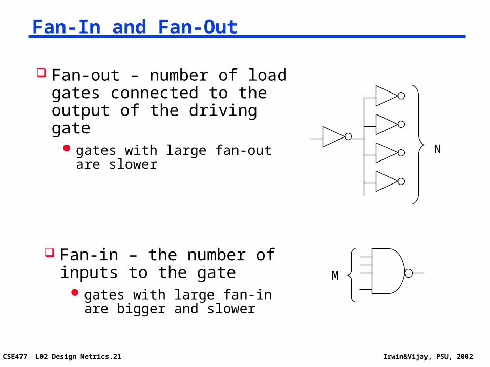
Fan-In and Fan-Out
Fan-out – number of load gates connected to the output of the driving gate
gates with large fan-out are slowerN
M
Fan-in – the number of inputs to the gate
gates with large fan-in are bigger and slower
CSE477 L02 Design Metrics.23 Irwin&Vijay, PSU, 2002
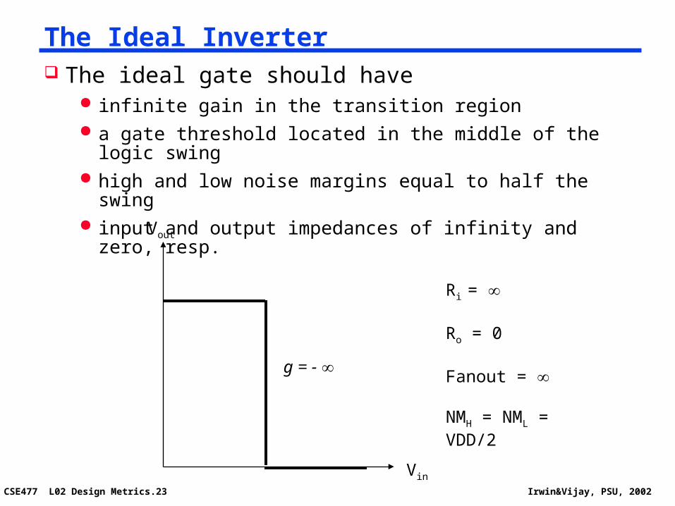
The Ideal Inverter The ideal gate should have
infinite gain in the transition region a gate threshold located in the middle of the logic swing high and low noise margins equal to half the swing input and output impedances of infinity and zero, resp.
g = -
Vout
Vin
Ri =
Ro = 0
Fanout =
NMH = NML = VDD/2
CSE477 L02 Design Metrics.25 Irwin&Vijay, PSU, 2002
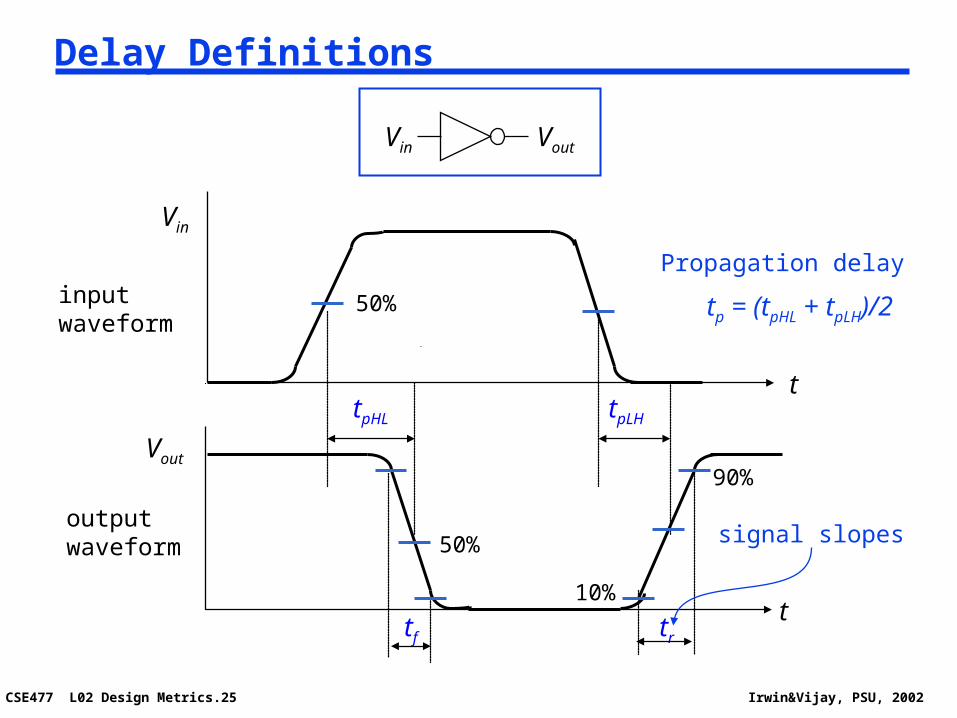
Delay Definitions
t
Vout
Vin
inputwaveform
outputwaveform
tp = (tpHL + tpLH)/2
Propagation delay
t
50%
tpHL
50%
tpLH
tf
90%
10%
tr
signal slopes
Vin Vout
CSE477 L02 Design Metrics.26 Irwin&Vijay, PSU, 2002
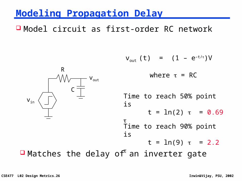
Modeling Propagation Delay
Model circuit as first-order RC network
R
C
vin
vout
vout (t) = (1 – e–t/)V
where = RC
Time to reach 50% point ist = ln(2) = 0.69
Time to reach 90% point ist = ln(9) = 2.2
Matches the delay of an inverter gate
CSE477 L02 Design Metrics.27 Irwin&Vijay, PSU, 2002
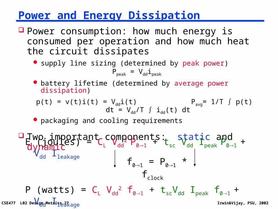
Power and Energy Dissipation Power consumption: how much energy is consumed
per operation and how much heat the circuit dissipates supply line sizing (determined by peak power)
Ppeak = Vddipeak
battery lifetime (determined by average power dissipation)
p(t) = v(t)i(t) = Vddi(t) Pavg= 1/T p(t) dt = Vdd/T idd(t) dt packaging and cooling requirements
Two important components: static and dynamic
E (joules) = CL Vdd2 P01 + tsc Vdd Ipeak P01 + Vdd Ileakage
P (watts) = CL Vdd2 f01 + tscVdd Ipeak f01 + Vdd Ileakage
f01 = P01 * fclock
CSE477 L02 Design Metrics.28 Irwin&Vijay, PSU, 2002
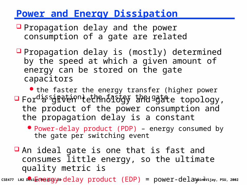
Power and Energy Dissipation Propagation delay and the power consumption of a gate
are related
Propagation delay is (mostly) determined by the speed at which a given amount of energy can be stored on the gate capacitors
the faster the energy transfer (higher power dissipation) the faster the gate
For a given technology and gate topology, the product of the power consumption and the propagation delay is a constant
Power-delay product (PDP) – energy consumed by the gate per switching event
An ideal gate is one that is fast and consumes little energy, so the ultimate quality metric is
Energy-delay product (EDP) = power-delay 2
CSE477 L02 Design Metrics.29 Irwin&Vijay, PSU, 2002
Digital integrated circuits have come a long way and still have quite some potential left for the coming decades
Some interesting challenges ahead Getting a clear perspective on the challenges and potential
solutions is the purpose of this course
Understanding the design metrics that govern digital design is crucial Cost, reliability, speed, power and energy dissipation
Summary
CSE477 L02 Design Metrics.30 Irwin&Vijay, PSU, 2002
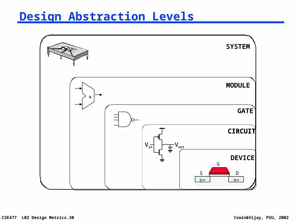
Design Abstraction Levels
SYSTEM
GATE
CIRCUIT
VoutVin
CIRCUIT
VoutVin
MODULE
+
DEVICE
n+S D
n+
G
CSE477 L02 Design Metrics.31 Irwin&Vijay, PSU, 2002
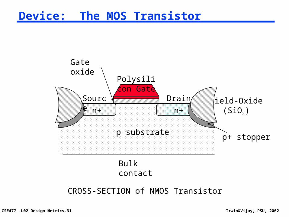
Device: The MOS Transistor
Gate oxide
n+
Source Drain
p substrate
Bulk contact
CROSS-SECTION of NMOS Transistor
p+ stopper
Field-Oxide(SiO2)n+
Polysilicon Gate

CSE477 L02 Design Metrics.32 Irwin&Vijay, PSU, 2002
Circuit: The CMOS Inverter
VDD
Vout
CL
Vin
Related Documents