CSE 490/590, Spring 2011 CSE 490/590 Computer Architecture Cache I Steve Ko Computer Sciences and Engineering University at Buffalo

CSE 490/590, Spring 2011 CSE 490/590 Computer Architecture Cache I Steve Ko Computer Sciences and Engineering University at Buffalo.
Dec 19, 2015
Welcome message from author
This document is posted to help you gain knowledge. Please leave a comment to let me know what you think about it! Share it to your friends and learn new things together.
Transcript

CSE 490/590, Spring 2011
CSE 490/590 Computer Architecture
Cache I
Steve KoComputer Sciences and Engineering
University at Buffalo

CSE 490/590, Spring 2011 2
Last Time…• Pipelining hazards
– Structural hazards– Data hazards– Control hazards
• Data hazards– Stall– Bypass
• Control hazards– Jump– Conditional branch

CSE 490/590, Spring 2011 3
Branch Delay Slots(expose control hazard to software)
• Change the ISA semantics so that the instruction that follows a jump or branch is always executed– gives compiler the flexibility to put in a useful instruction where
normally a pipeline bubble would have resulted.
I1 096 ADD I2 100 BEQZ r1 +200I3 104 ADDI4 304 ADD
Delay slot instruction executed regardless of
branch outcome
• Other techniques include more advanced branch prediction, which can dramatically reduce the branch penalty... to come later

CSE 490/590, Spring 2011 4
timet0 t1 t2 t3 t4 t5 t6 t7 . . . .IF I1 I2 I3 I4ID I1 I2 I3 I4EX I1 I2 I3 I4MA I1 I2 I3 I4WB I1 I2 I3 I4
Branch Pipeline Diagrams(branch delay slot)
timet0 t1 t2 t3 t4 t5 t6 t7 . . . .
(I1) 096: ADD IF1 ID1 EX1 MA1 WB1
(I2) 100: BEQZ +200 IF2 ID2 EX2 MA2 WB2
(I3) 104: ADD IF3 ID3 EX3 MA3 WB3
(I4) 304: ADD IF4 ID4 EX4 MA4 WB4
Resource Usage

CSE 490/590, Spring 2011 5
Why an Instruction may not be dispatched every cycle (CPI>1)
• Full bypassing may be too expensive to implement– typically all frequently used paths are provided– some infrequently used bypass paths may increase cycle time and
counteract the benefit of reducing CPI
• Loads have two-cycle latency– Instruction after load cannot use load result– MIPS-I ISA defined load delay slots, a software-visible pipeline hazard
(compiler schedules independent instruction or inserts NOP to avoid hazard). Removed in MIPS-II (pipeline interlocks added in hardware)
» MIPS:“Microprocessor without Interlocked Pipeline Stages”
• Conditional branches may cause bubbles– kill following instruction(s) if no delay slots

CSE 490/590, Spring 2011 6
Early Read-Only Memory Technologies
Punched cards, From early 1700s through Jaquard Loom, Babbage, and then IBM
Punched paper tape, instruction stream in Harvard Mk 1
IBM Card Capacitor ROS
IBM Balanced Capacitor ROS
Diode Matrix, EDSAC-2 µcode store

CSE 490/590, Spring 2011 7
Early Read/Write Main Memory Technologies
Williams Tube, Manchester Mark 1, 1947
Babbage, 1800s: Digits stored on mechanical wheels
Mercury Delay Line, Univac 1, 1951
Also, regenerative capacitor memory on Atanasoff-Berry computer, and rotating magnetic drum memory on IBM 650

CSE 490/590, Spring 2011 8
Semiconductor Memory
• Semiconductor memory began to be competitive in early 1970s– Intel formed to exploit market for semiconductor memory– Early semiconductor memory was Static RAM (SRAM). SRAM
cell internals similar to a latch (cross-coupled inverters).
• First commercial Dynamic RAM (DRAM) was Intel 1103– 1Kbit of storage on single chip– charge on a capacitor used to hold value
• Semiconductor memory quickly replaced core in ‘70s

CSE 490/590, Spring 2011 9
Modern DRAM Structure
[Samsung, sub-70nm DRAM, 2004]

CSE 490/590, Spring 2011 10
DRAM Architecture
Row
Ad
dre
ss
Deco
der
Col.1
Col.2M
Row 1
Row 2N
Column Decoder & Sense Amplifiers
M
N
N+M
bit linesword lines
Memory cell(one bit)
DData
• Bits stored in 2-dimensional arrays on chip
• Modern chips have around 4 logical banks on each chip– each logical bank physically implemented as many smaller arrays
CSE 490/590, Spring 2011 11
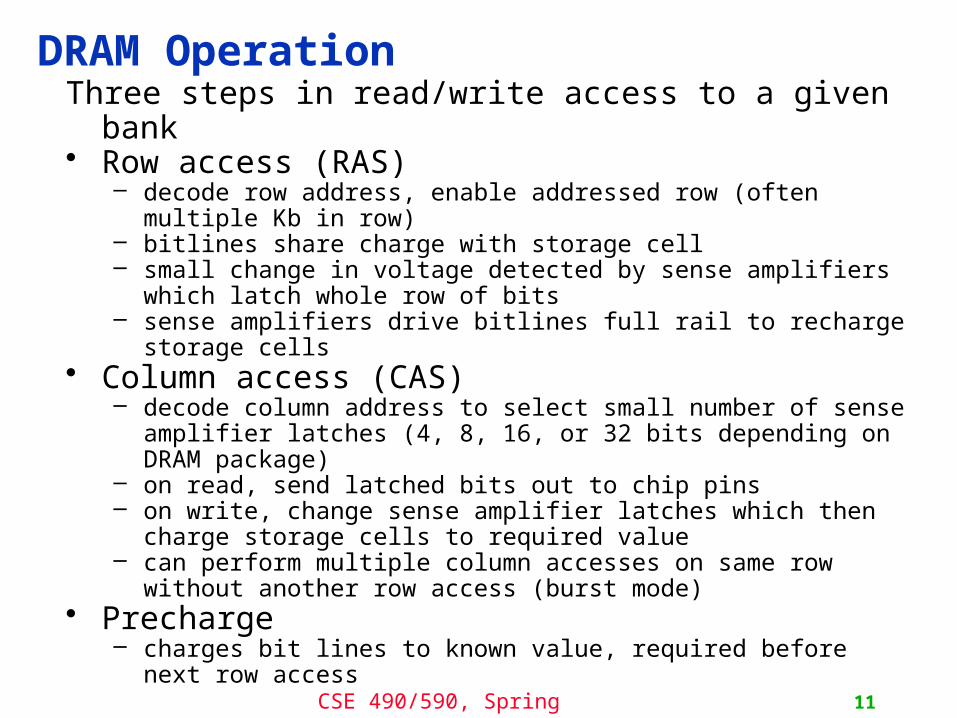
DRAM OperationThree steps in read/write access to a given bank• Row access (RAS)
– decode row address, enable addressed row (often multiple Kb in row)– bitlines share charge with storage cell– small change in voltage detected by sense amplifiers which latch whole
row of bits– sense amplifiers drive bitlines full rail to recharge storage cells
• Column access (CAS)– decode column address to select small number of sense amplifier
latches (4, 8, 16, or 32 bits depending on DRAM package)– on read, send latched bits out to chip pins– on write, change sense amplifier latches which then charge storage
cells to required value– can perform multiple column accesses on same row without another
row access (burst mode)• Precharge
– charges bit lines to known value, required before next row access
Each step has a latency of around 15-20ns in modern DRAMsVarious DRAM standards (DDR, RDRAM) have different ways of encoding the
signals for transmission to the DRAM, but all share same core architecture

CSE 490/590, Spring 2011 12
DRAM Packaging
• DIMM (Dual Inline Memory Module) contains multiple chips with clock/control/address signals connected in parallel (sometimes need buffers to drive signals to all chips)
• Data pins work together to return wide word (e.g., 64-bit data bus using 16x4-bit parts)
Address lines multiplexed row/column address
Clock and control signals
Data bus(4b,8b,16b,32b)
DRAM chip
~12
~7
CSE 490/590, Spring 2011 13
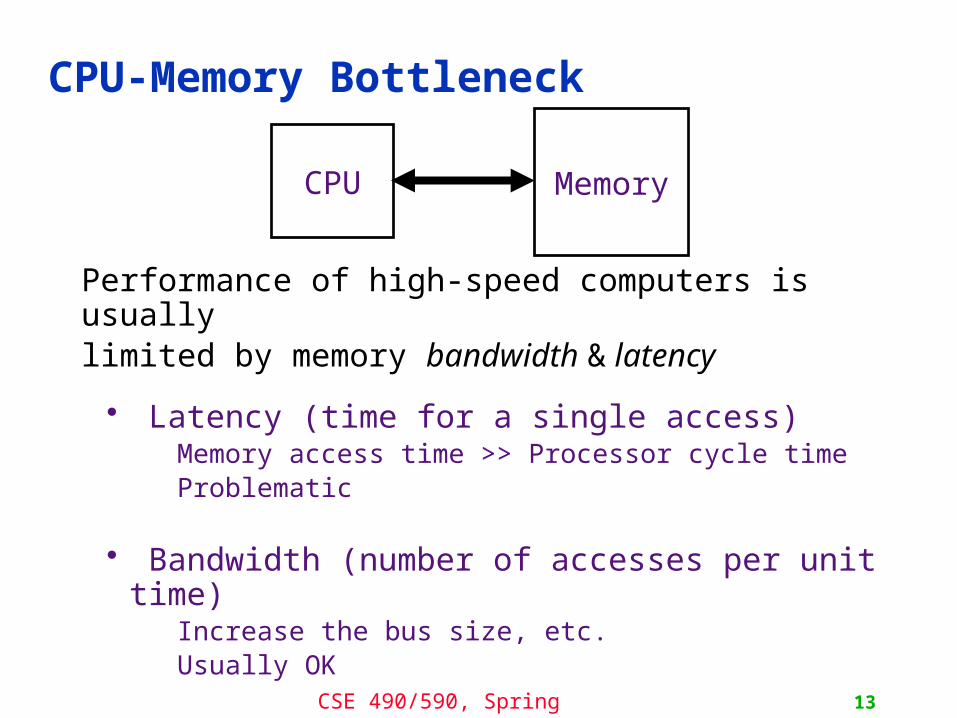
CPU-Memory Bottleneck
MemoryCPU
Performance of high-speed computers is usuallylimited by memory bandwidth & latency
• Latency (time for a single access)Memory access time >> Processor cycle timeProblematic
• Bandwidth (number of accesses per unit time)Increase the bus size, etc.Usually OK
CSE 490/590, Spring 2011 14
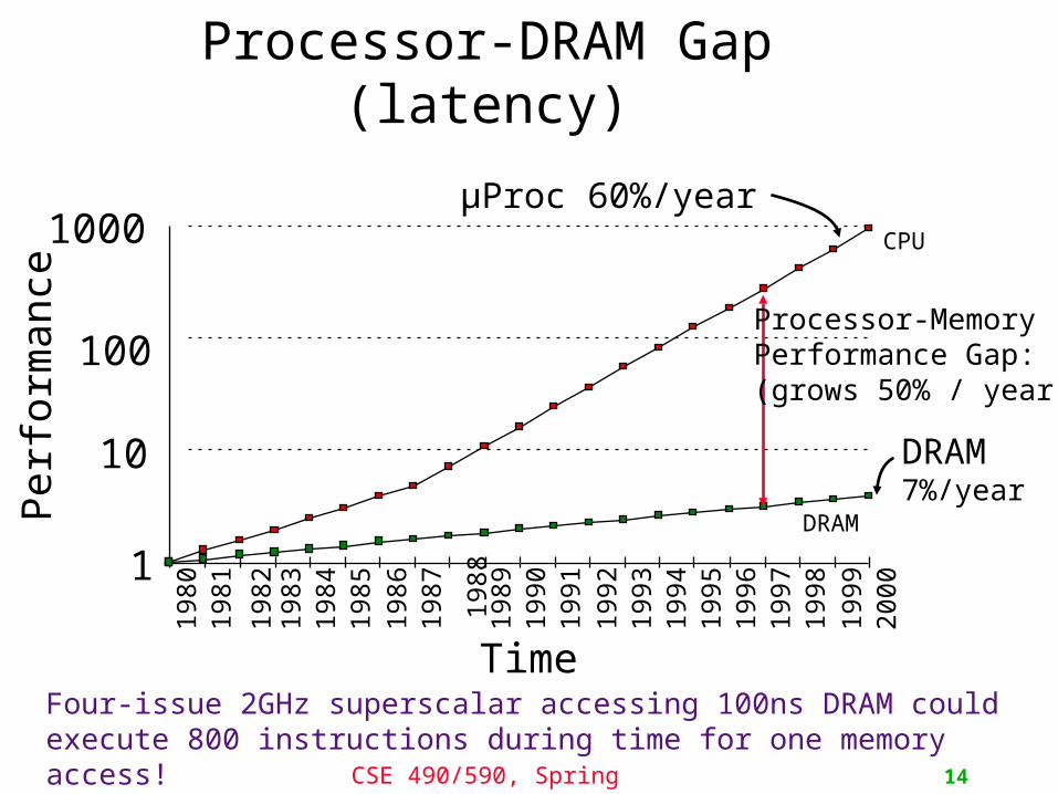
Processor-DRAM Gap (latency)
Time
µProc 60%/year
DRAM7%/year
1
10
100
1000198
0198
1
198
3198
4198
5198
6198
7
198
8198
9199
0199
1199
2199
3199
4199
5199
6199
7199
8199
9200
0
DRAM
CPU198
2
Processor-MemoryPerformance Gap:(grows 50% / year)
Perf
orm
ance
Four-issue 2GHz superscalar accessing 100ns DRAM could execute 800 instructions during time for one memory access!

CSE 490/590, Spring 2011 15
Physical Size Affects Latency
Small Memory
CPU
Big Memory
CPU
• Signals have further to travel
• Fan out to more locations

CSE 490/590, Spring 2011 16
CSE 490/590 Administrivia
• Very important to attend– Recitations next week & the week after
• Guest lectures– There will be a couple guest lectures late Feb/early Mar.
• Quiz 1– Rescheduled– Fri, 2/11– Closed book, in-class– Includes lectures until last Monday (1/31)– Review: next Wed (2/9)
CSE 490/590, Spring 2011 17
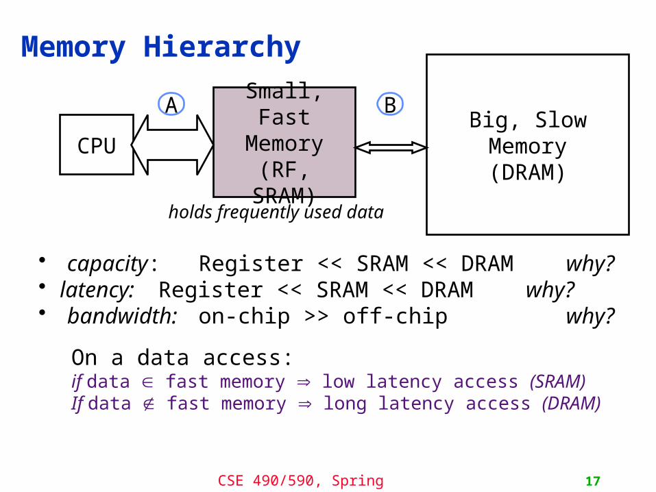
Memory Hierarchy
Small,Fast
Memory(RF, SRAM)
• capacity: Register << SRAM << DRAM why?• latency: Register << SRAM << DRAM why?• bandwidth: on-chip >> off-chip why?
On a data access:if data Î fast memory low latency access (SRAM)If data Ï fast memory long latency access (DRAM)
CPUBig, Slow Memory(DRAM)
A B
holds frequently used data

CSE 490/590, Spring 2011 18
Relative Memory Cell Sizes
[ Foss, “Implementing Application-Specific
Memory”, ISSCC 1996 ]
DRAM on memory chip
On-Chip SRAM in logic chip
CSE 490/590, Spring 2011 19
Levels of the Memory Hierarchy
CPU Registers100s Bytes<10s ns
CacheK Bytes10-100 ns1-0.1 cents/bit
Main MemoryM Bytes200ns- 500ns$.0001-.00001 cents /bit
DiskG Bytes, 10 ms (10,000,000 ns)
10 - 10 cents/bit-5 -6
CapacityAccess TimeCost
Tapeinfinitesec-min10 -8
Registers
Cache
Memory
Disk
Tape
Instr. Operands
Blocks
Pages
Files
StagingXfer Unit
prog./compiler1-8 bytes
cache cntl8-128 bytes
OS512-4K bytes
user/operatorMbytes
Upper Level
Lower Level
faster
Larger
CSE 490/590, Spring 2011
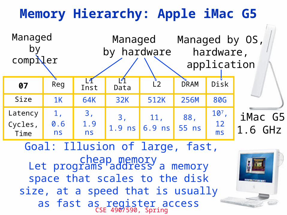
Memory Hierarchy: Apple iMac G5
iMac G51.6 GHz
07 Reg L1 Inst L1 Data L2 DRAM Disk
Size 1K 64K 32K 512K 256M 80G
Latency
Cycles, Time
1,
0.6 ns
3,
1.9 ns
3,
1.9 ns
11,
6.9 ns
88,
55 ns
107,
12 ms
Let programs address a memory space that scales to the disk size, at a speed
that is usually as fast as register access
Managed by compiler
Managed by hardware
Managed by OS,hardware,application
Goal: Illusion of large, fast, cheap memory

CSE 490/590, Spring 2011 21
Management of Memory Hierarchy
• Small/fast storage, e.g., registers– Address usually specified in instruction– Generally implemented directly as a register file
» but hardware might do things behind software’s back, e.g., stack management, register renaming
• Larger/slower storage, e.g., main memory– Address usually computed from values in register– Generally implemented as a hardware-managed
cache hierarchy» hardware decides what is kept in fast memory» but software may provide “hints”, e.g., don’t cache or
prefetch
CSE 490/590, Spring 2011
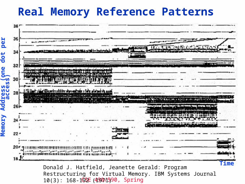
Real Memory Reference Patterns
Donald J. Hatfield, Jeanette Gerald: Program Restructuring for Virtual Memory. IBM Systems Journal 10(3): 168-192 (1971)
Time
Mem
ory
Ad
dre
ss (
on
e d
ot
per
acc
ess)

CSE 490/590, Spring 2011
Typical Memory Reference PatternsAddress
Time
Instruction fetches
Stackaccesses
Dataaccesses
n loop iterations
subroutine call
subroutine return
argument access
vector access
scalar accesses

CSE 490/590, Spring 2011
Common Predictable Patterns
Two predictable properties of memory references:
– Temporal Locality: If a location is referenced it is likely to be referenced again in the near future.
– Spatial Locality: If a location is referenced it is likely that locations near it will be referenced in the near future.

CSE 490/590, Spring 2011
Memory Reference Patterns
Donald J. Hatfield, Jeanette Gerald: Program Restructuring for Virtual Memory. IBM Systems Journal 10(3): 168-192 (1971)
Time
Mem
ory
Ad
dre
ss (
on
e d
ot
per
acc
ess)
SpatialLocality
Temporal Locality

CSE 490/590, Spring 2011
Caches
Caches exploit both types of predictability:
– Exploit temporal locality by remembering the contents of recently accessed locations.
– Exploit spatial locality by fetching blocks of data around recently accessed locations.
CSE 490/590, Spring 2011
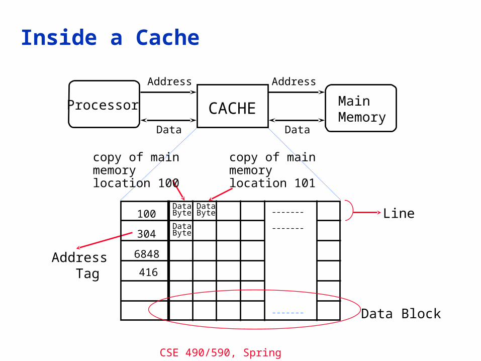
Inside a Cache
CACHEProcessor MainMemory
Address Address
DataData
Address Tag
Data Block
DataByte
DataByte
DataByte
Line100
304
6848
copy of mainmemorylocation 100
copy of mainmemorylocation 101
416

CSE 490/590, Spring 2011
Cache Algorithm (Read)
Look at Processor Address, search cache tags to find match. Then either
Found in cachea.k.a. HIT
Return copyof data fromcache
Not in cachea.k.a. MISS
Read block of data fromMain Memory
Wait …
Return data to processorand update cache
Q: Which line do we replace?

CSE 490/590, Spring 2011 29
Placement Policy
0 1 2 3 4 5 6 70 1 2 3Set Number
Cache
Fully (2-way) Set DirectAssociative Associative Mappedanywhere anywhere in only into
set 0 block 4 (12 mod 4) (12 mod 8)
0 1 2 3 4 5 6 7 8 91 1 1 1 1 1 1 1 1 1 0 1 2 3 4 5 6 7 8 9
2 2 2 2 2 2 2 2 2 2 0 1 2 3 4 5 6 7 8 9
3 30 1
Memory
Block Number
block 12 can be placed

CSE 490/590, Spring 2011
Direct-Mapped Cache
Tag Data Block V
=
BlockOffset
Tag Index
t k b
t
HIT Data Word or Byte
2k
lines

CSE 490/590, Spring 2011
Direct Map Address Selectionhigher-order vs. lower-order address bits
Tag Data Block V
=
BlockOffset
Index
t k b
t
HIT Data Word or Byte
2k
lines
Tag

CSE 490/590, Spring 2011
2-Way Set-Associative Cache
Tag Data Block V
=
BlockOffset
Tag Index
t k
b
HIT
Tag Data Block V
DataWordor Byte
=
t

CSE 490/590, Spring 2011
Fully Associative Cache
Tag Data Block V
=
Blo
ckO
ffse
t
Tag
t
b
HIT
DataWordor Byte
=
=
t

CSE 490/590, Spring 2011 34
Replacement Policy
In an associative cache, which block from a set should be evicted when the set becomes full?
• Random
• Least Recently Used (LRU)• LRU cache state must be updated on every access• true implementation only feasible for small sets (2-way)• pseudo-LRU binary tree often used for 4-8 way
• First In, First Out (FIFO) a.k.a. Round-Robin• used in highly associative caches
• Not Least Recently Used (NLRU)• FIFO with exception for most recently used block or blocks
This is a second-order effect. Why?
Replacement only happens on misses
CSE 490/590, Spring 2011 35
Acknowledgements
• These slides heavily contain material developed and copyright by
– Krste Asanovic (MIT/UCB)– David Patterson (UCB)
• And also by:– Arvind (MIT)– Joel Emer (Intel/MIT)– James Hoe (CMU)– John Kubiatowicz (UCB)
• MIT material derived from course 6.823• UCB material derived from course CS252
Related Documents