CSC 2400 Computer Systems I Lecture 4 Processor Architecture

CSC 2400 Computer Systems I Lecture 4 Processor Architecture.
Dec 19, 2015
Welcome message from author
This document is posted to help you gain knowledge. Please leave a comment to let me know what you think about it! Share it to your friends and learn new things together.
Transcript

CSC 2400Computer Systems I
Lecture 4
Processor Architecture
The Stored Program Computer
3
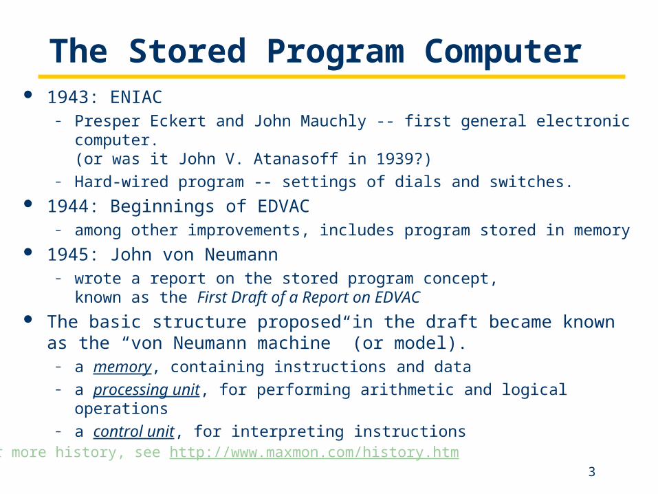
The Stored Program Computer 1943: ENIAC
– Presper Eckert and John Mauchly -- first general electronic computer.(or was it John V. Atanasoff in 1939?)
– Hard-wired program -- settings of dials and switches. 1944: Beginnings of EDVAC
– among other improvements, includes program stored in memory 1945: John von Neumann
– wrote a report on the stored program concept, known as the First Draft of a Report on EDVAC
The basic structure proposed in the draft became knownas the “von Neumann machine” (or model).
– a memory, containing instructions and data– a processing unit, for performing arithmetic and logical operations– a control unit, for interpreting instructions
For more history, see http://www.maxmon.com/history.htm

4
Von Neumann Model
MAR MDR
PC IR

5
Memory 2k x m array of stored bits Address
– unique (k-bit) identifier of location
Contents– m-bit value stored in location
Basic Operations: LOAD
– read a value from a memory location
STORE– write a value to a memory location
•••
0000000100100011010001010110
110111101111
00101101
10100010
6
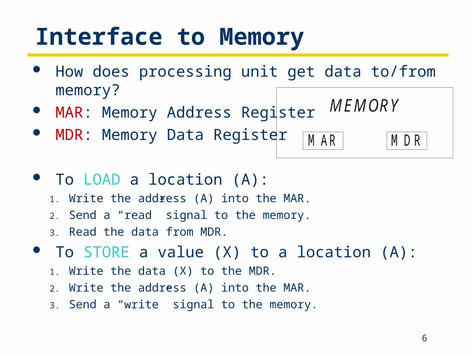
Interface to Memory How does processing unit get data to/from memory? MAR: Memory Address Register MDR: Memory Data Register
To LOAD a location (A):1. Write the address (A) into the MAR.
2. Send a “read” signal to the memory.
3. Read the data from MDR.
To STORE a value (X) to a location (A):1. Write the data (X) to the MDR.
2. Write the address (A) into the MAR.
3. Send a “write” signal to the memory.
M E M OR Y
M AR M D R
7
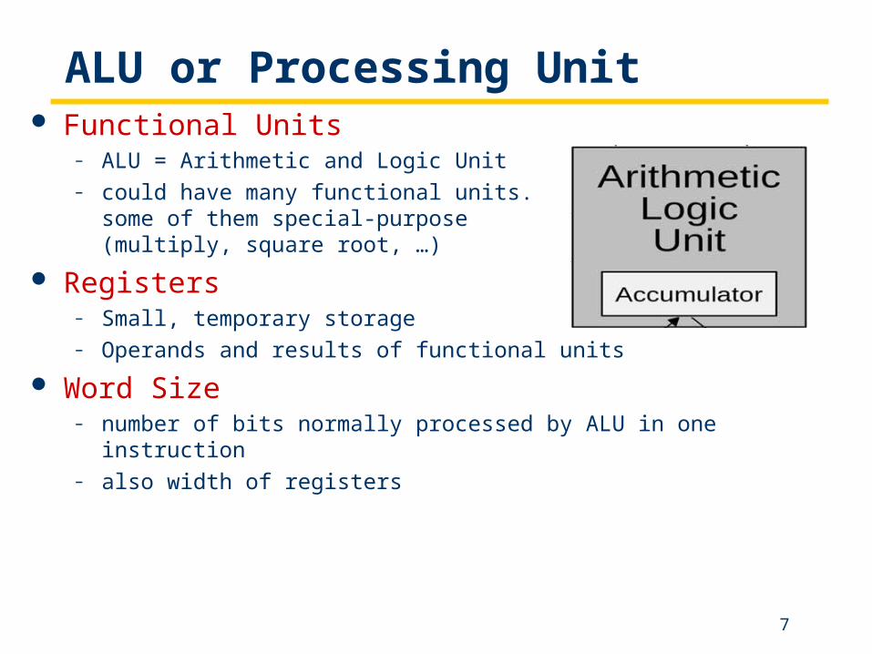
ALU or Processing Unit Functional Units
– ALU = Arithmetic and Logic Unit– could have many functional units.
some of them special-purpose(multiply, square root, …)
Registers– Small, temporary storage– Operands and results of functional units
Word Size– number of bits normally processed by ALU in one instruction– also width of registers

8
Input and Output Devices for getting data into and out of computer memory
Each device has its own interface,usually a set of registers like thememory’s MAR and MDR
– keyboard: data register (KBDR) and status register (KBSR)– monitor: data register (DDR) and status register (DSR)
Some devices provide both input and output– disk, network
Program that controls access to a device is usually called a driver.
IN P UTK eybo ardM ouseS c annerD is k
OUTP UTM on ito rP rin terLE DD is k
9
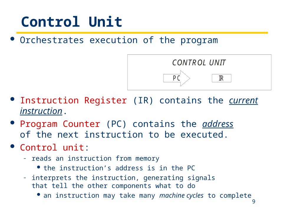
Control Unit Orchestrates execution of the program
Instruction Register (IR) contains the current instruction. Program Counter (PC) contains the address
of the next instruction to be executed. Control unit:
– reads an instruction from memory the instruction’s address is in the PC
– interprets the instruction, generating signals that tell the other components what to do
an instruction may take many machine cycles to complete
CON TR OL UN IT
IRP C
Logic Design
11
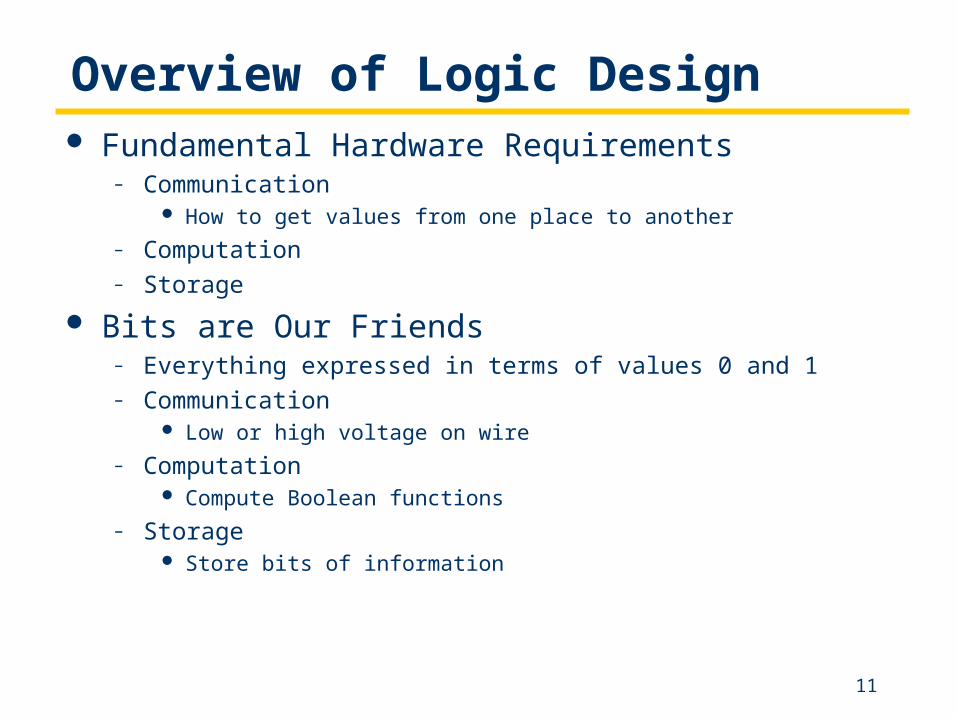
Overview of Logic Design Fundamental Hardware Requirements
– Communication How to get values from one place to another
– Computation– Storage
Bits are Our Friends– Everything expressed in terms of values 0 and 1– Communication
Low or high voltage on wire
– Computation Compute Boolean functions
– Storage Store bits of information
12
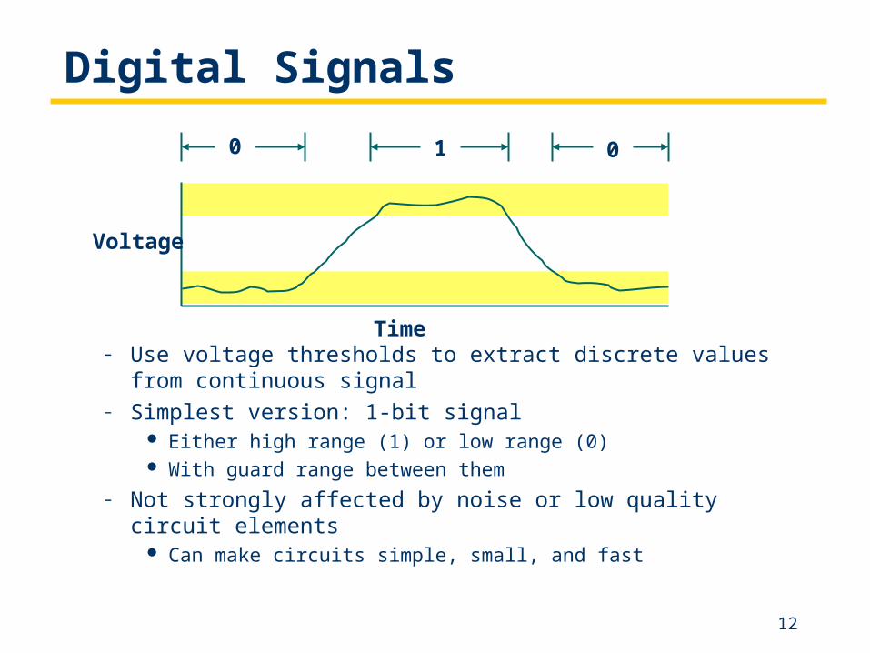
Digital Signals
– Use voltage thresholds to extract discrete values from continuous signal
– Simplest version: 1-bit signal Either high range (1) or low range (0) With guard range between them
– Not strongly affected by noise or low quality circuit elements Can make circuits simple, small, and fast
Voltage
Time
0 1 0
13
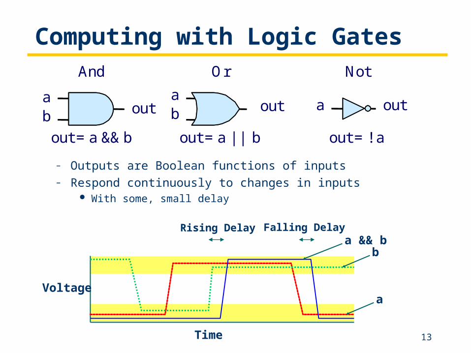
Computing with Logic Gates
– Outputs are Boolean functions of inputs– Respond continuously to changes in inputs
With some, small delay
ab out
ab out a out
out = a && b out = a || b out = !a
And Or Not
Voltage
Time
a
ba && b
Rising Delay Falling Delay
14
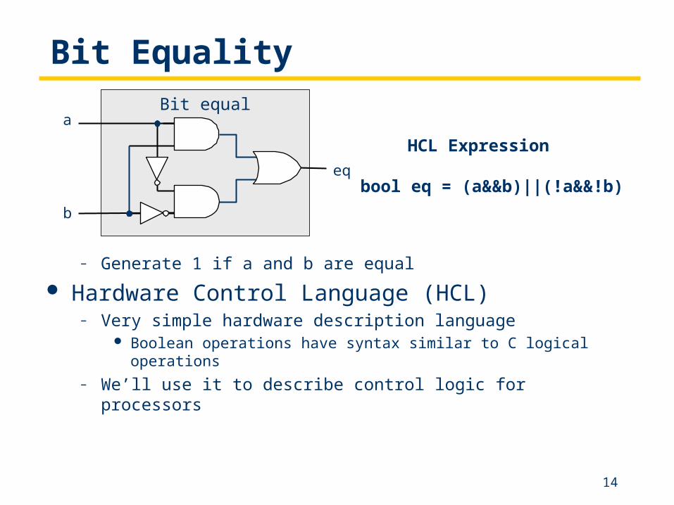
Bit Equality
– Generate 1 if a and b are equal
Hardware Control Language (HCL)– Very simple hardware description language
Boolean operations have syntax similar to C logical operations
– We’ll use it to describe control logic for processors
Bit equala
b
eqbool eq = (a&&b)||(!a&&!b)
HCL Expression

15
Word Equality
– 32-bit word size– HCL representation
Equality operation Generates Boolean value
b31Bit equal
a31
eq31
b30Bit equal
a30
eq30
b1Bit equal
a1
eq1
b0Bit equal
a0
eq0
Eq
==B
A
Eq
Word-Level Representation
bool Eq = (A == B)
HCL Representation
16
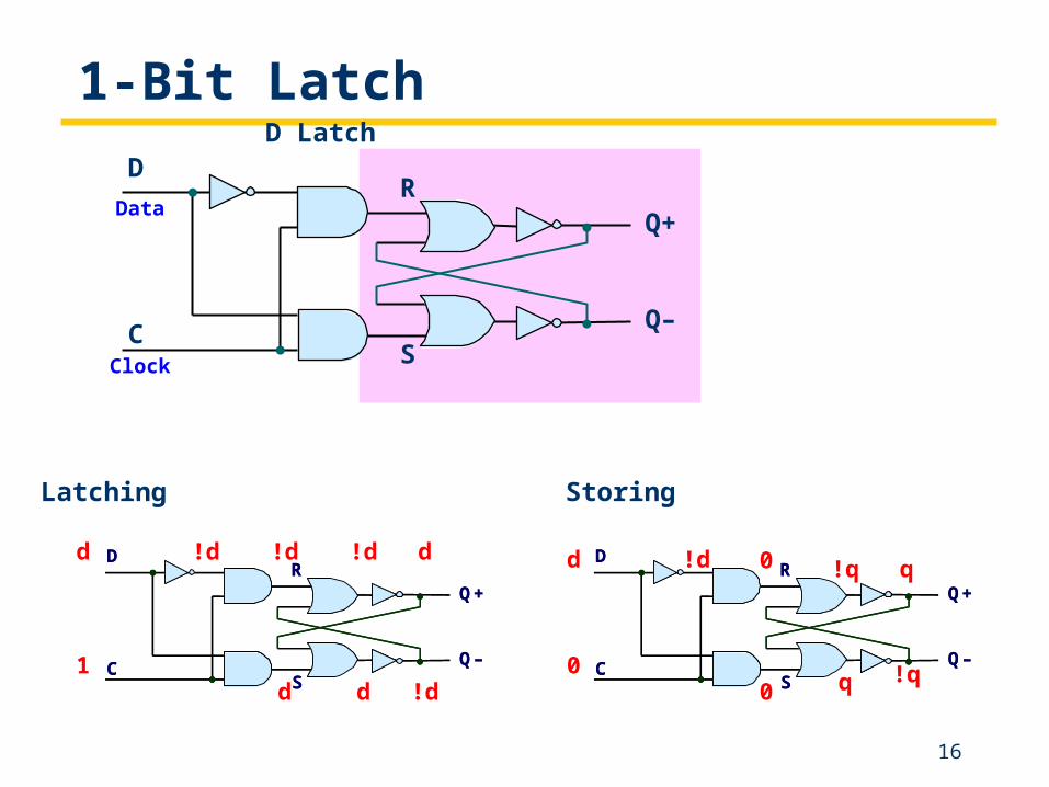
1-Bit LatchD Latch
Q+
Q–
R
S
D
C
Data
Clock
Latching
1
Q+
Q–
R
S
D
C
Q+
Q–
R
S
D
C
d !d !d !d d
d d !d0
Storing
Q+
Q–
R
S
D
C
Q+
Q–
R
S
D
C
d !d q
!q
!q
q0
0
17
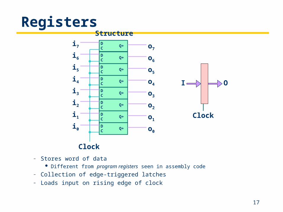
Registers
– Stores word of data Different from program registers seen in assembly code
– Collection of edge-triggered latches– Loads input on rising edge of clock
I O
Clock
DC
Q+
DC
Q+
DC
Q+
DC
Q+
DC
Q+
DC
Q+
DC
Q+
DC
Q+
i7
i6
i5
i4
i3
i2
i1
i0
o7
o6
o5
o4
o3
o2
o1
o0
Clock
Structure
18
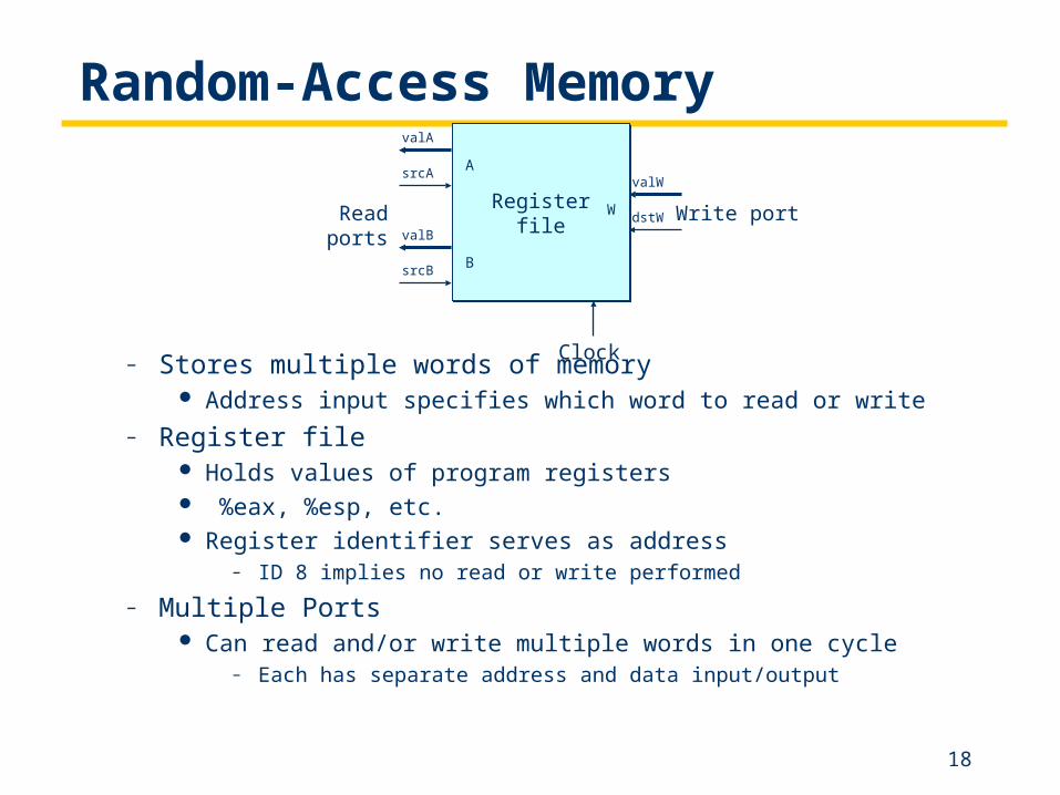
Random-Access Memory
– Stores multiple words of memory Address input specifies which word to read or write
– Register file Holds values of program registers %eax, %esp, etc. Register identifier serves as address
– ID 8 implies no read or write performed
– Multiple Ports Can read and/or write multiple words in one cycle
– Each has separate address and data input/output
Registerfile
Registerfile
A
B
W dstW
srcA
valA
srcB
valB
valW
Read ports Write port
Clock

19
Basic Logic Gates
NOTE: okay to use just a circle for NOT:

20
More than 2 Inputs? AND/OR can take any number of inputs.
– AND = 1 if all inputs are 1.– OR = 1 if any input is 1.– Similar for NAND/NOR.
Can implement with multiple two-input gates

21
Logical Completeness Can implement ANY truth table with AND, OR, NOT.
A B C D
0 0 0 0
0 0 1 0
0 1 0 1
0 1 1 0
1 0 0 0
1 0 1 1
1 1 0 0
1 1 1 0
1. AND combinations that yield a "1" in the truth table.
2. OR the resultsof the AND gates.
22
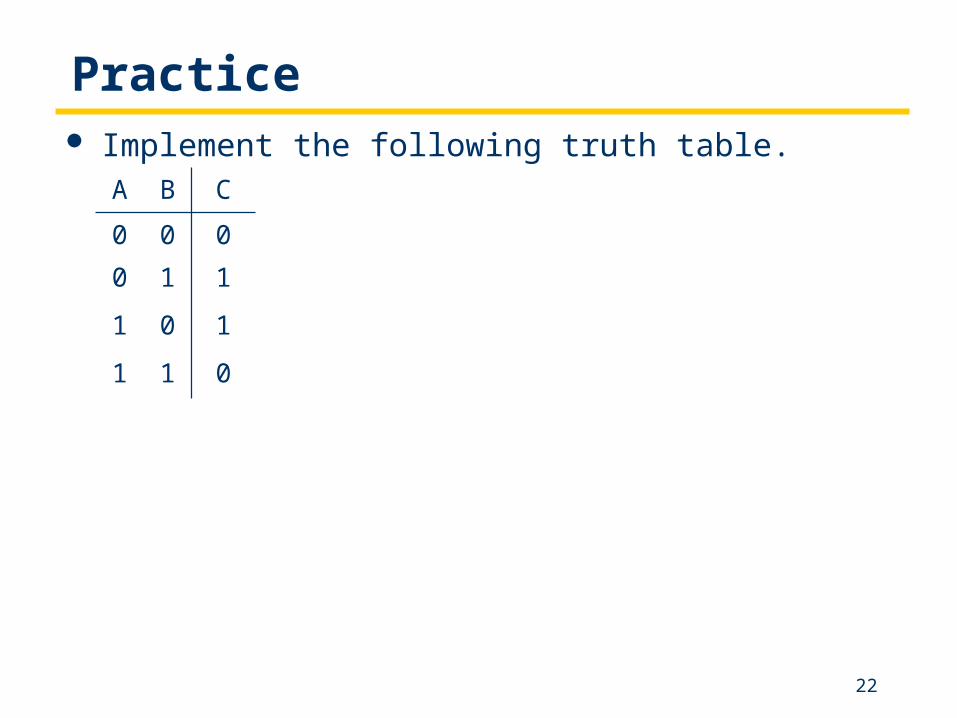
Practice Implement the following truth table.
A B C
0 0 0
0 1 1
1 0 1
1 1 0
23
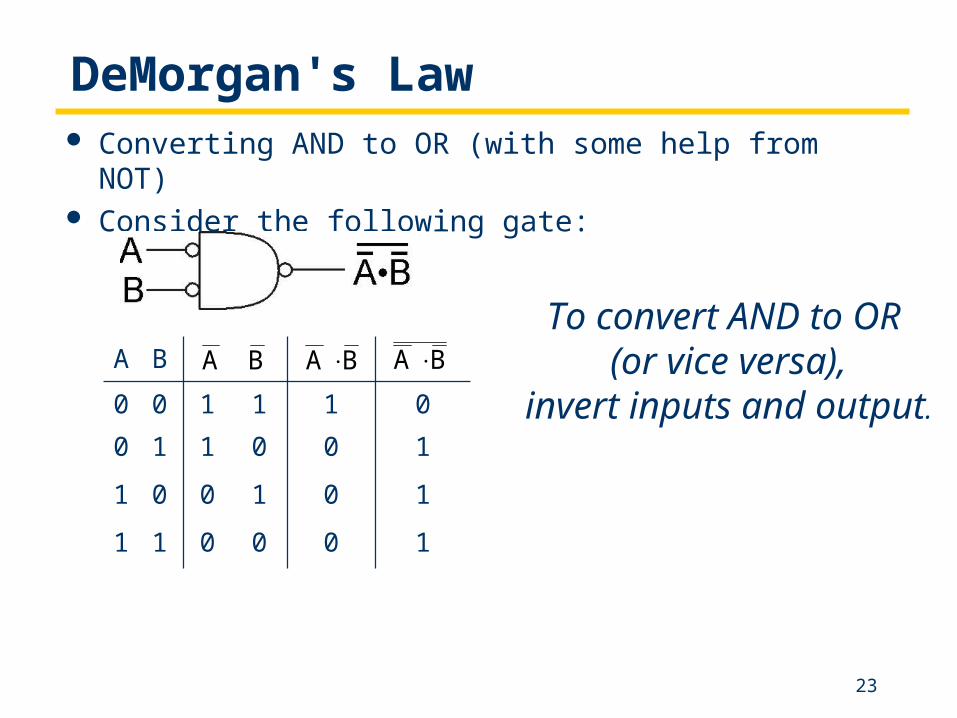
DeMorgan's Law Converting AND to OR (with some help from NOT) Consider the following gate:
A B
0 0 1 1 1 0
0 1 1 0 0 1
1 0 0 1 0 1
1 1 0 0 0 1
BA BA BA To convert AND to OR
(or vice versa),invert inputs and output.

24
Decoder n inputs, 2n outputs
– exactly one output is 1 for each possible input pattern
2-bitdecoder

Programming Wisdom

26
Solving Problems using a Computer Methodologies for creating computer programs
that perform a desired function.
Problem Solving– How do we figure out what to tell the computer to do?– Convert problem statement into algorithm,
using stepwise refinement.
Debugging– How do we figure out why it didn’t work?– Examining registers and memory, setting breakpoints, etc.
Time spent on the first can reduce time spent on the second!

27
Stepwise Refinement Also known as systematic decomposition.
Start with problem statement: “We wish to count the number of occurrences of a character
in a file. The character in question is to be input fromthe keyboard; the result is to be displayed on the monitor.”
Decompose task into a few simpler subtasks.
Decompose each subtask into smaller subtasks,and these into even smaller subtasks, etc....until you get to the machine instruction level.
28
Problem Statement Because problem statements are written in English,
they are sometimes ambiguous and/or incomplete.– Where is “file” located? How big is it, or how do I know
when I’ve reached the end?– How should final count be printed? A decimal number?– If the character is a letter, should I count both
upper-case and lower-case occurrences?
How do you resolve these issues?– Ask the person who wants the problem solved, or– Make a decision and document it.
29
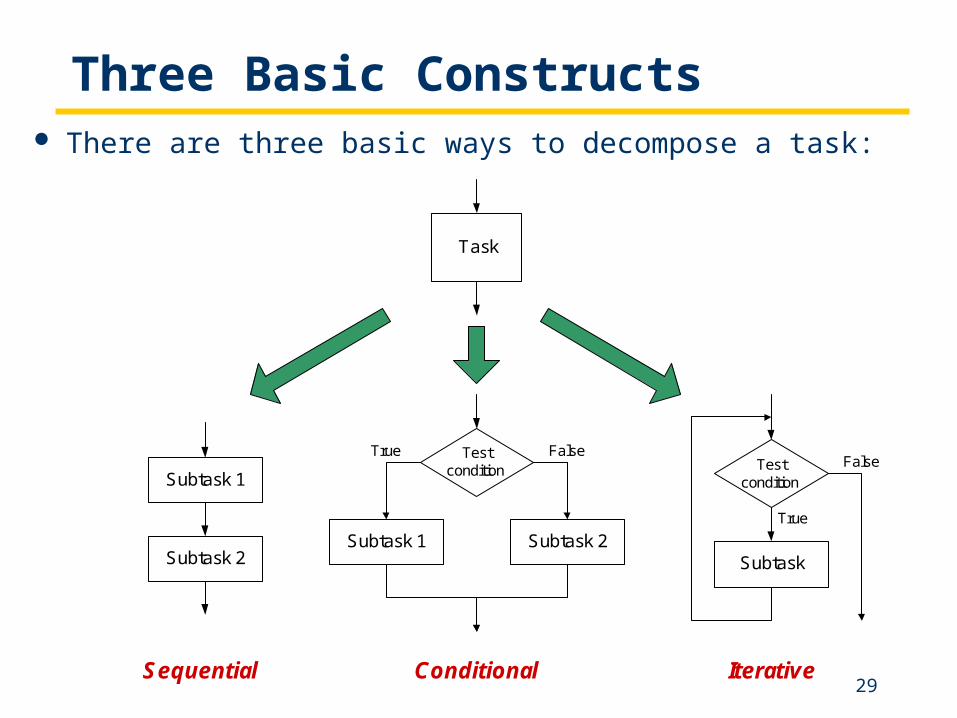
Three Basic Constructs There are three basic ways to decompose a task:
Task
Subtask 1
Subtask 2Subtask 1 Subtask 2
Testcondition
Subtask
Testcondition
Sequential Conditional Iterative
True
True
FalseFalse

30
Sequential Do Subtask 1 to completion,
then do Subtask 2 to completion, etc.
Get characterinput fromkeyboard
Examine file andcount the numberof characters that
match
Print numberto the screen
Count and print theoccurrences of acharacter in a file
31
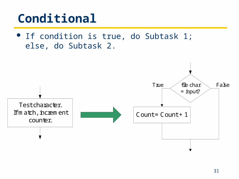
Conditional If condition is true, do Subtask 1;
else, do Subtask 2.
Test character.If match, increment
counter.Count = Count + 1
file char= input?
True False
32
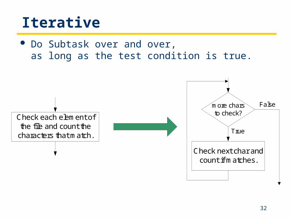
Iterative Do Subtask over and over,
as long as the test condition is true.
Check each element ofthe file and count the
characters that match.
Check next char andcount if matches.
more charsto check?
True
False

33
Problem Solving Skills Learn to convert problem statement
into step-by-step description of subtasks.
– Like a puzzle, or a “word problem” from grammar school math. What is the starting state of the system? What is the desired ending state? How do we move from one state to another?
– Recognize English words that correlate to three basic constructs: “do A then do B” sequential “if G, then do H” conditional “for each X, do Y” iterative “do Z until W” iterative
34
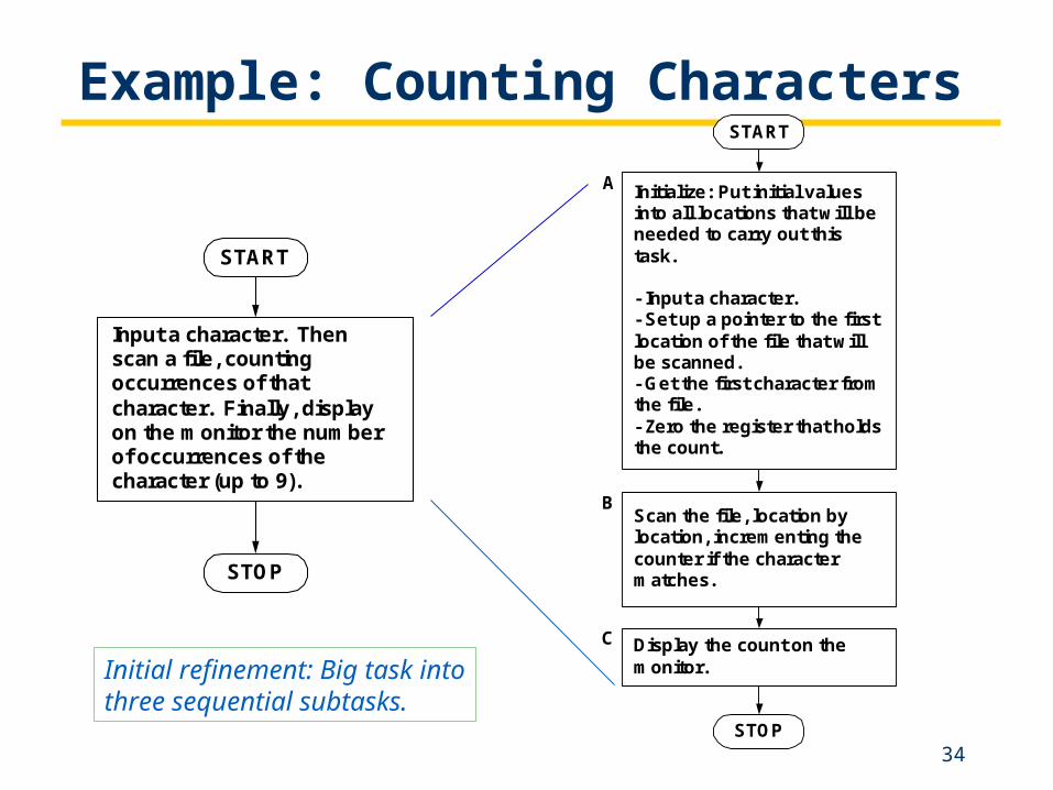
Example: Counting Characters
Input a character. Thenscan a file, countingoccurrences of thatcharacter. Finally, displayon the monitor the numberof occurrences of thecharacter (up to 9).
START
STOP
Initialize: Put initial valuesinto all locations that will beneeded to carry out thistask.
- Input a character.- Set up a pointer to the firstlocation of the file that willbe scanned.- Get the first character fromthe file.- Zero the register that holdsthe count.
START
STOP
Scan the file, location bylocation, incrementing thecounter if the charactermatches.
Display the count on themonitor.
A
B
C
Initial refinement: Big task intothree sequential subtasks.
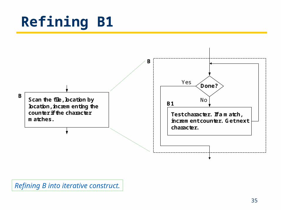
35
Refining B1
Scan the file, location bylocation, incrementing thecounter if the charactermatches.
B
Test character. If a match,increment counter. Get nextcharacter.
B1
Done?
No
Yes
B
Refining B into iterative construct.
36
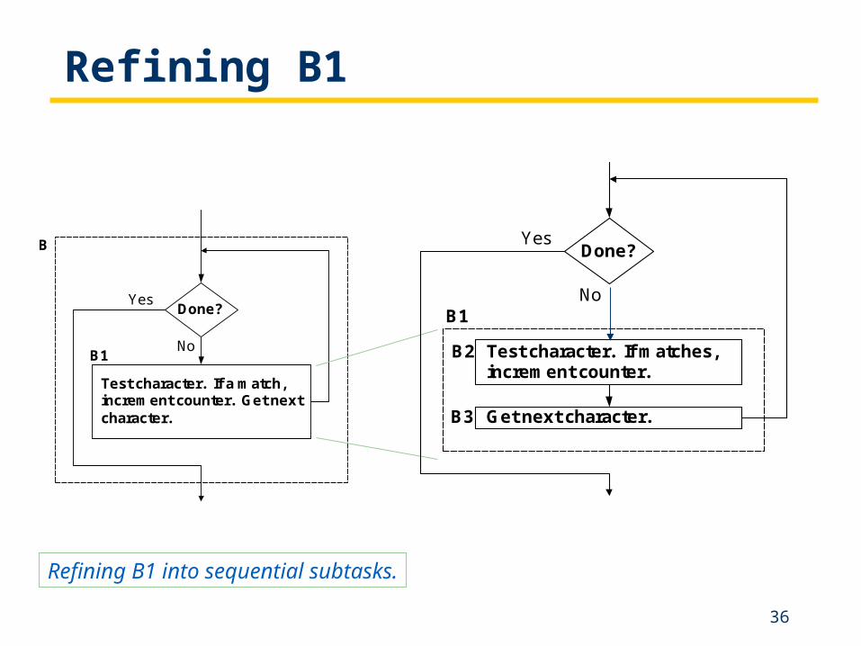
Refining B1
Refining B1 into sequential subtasks.
Test character. If a match,increment counter. Get nextcharacter.
B1
Done?
No
Yes
B
Get next character.
B1
Done?
No
Yes
Test character. If matches,increment counter.
B2
B3
37
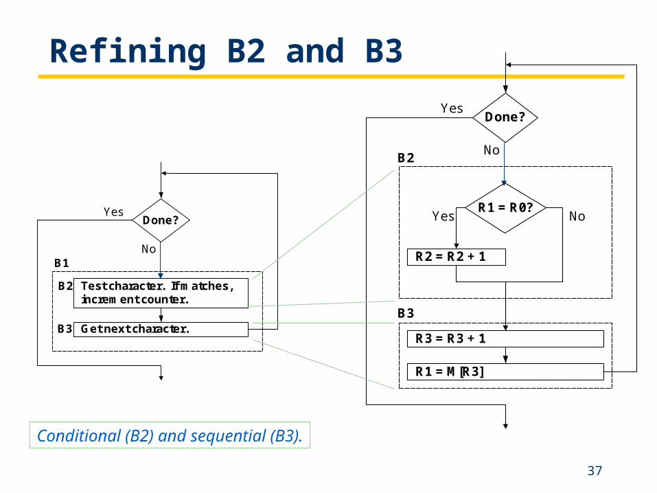
Refining B2 and B3
R1 = M[R3]
Done?
No
Yes
B2
B3
R3 = R3 + 1
R1 = R0?
R2 = R2 + 1
NoYes
Get next character.
B1
Done?
No
Yes
Test character. If matches,increment counter.
B2
B3
Conditional (B2) and sequential (B3).
38
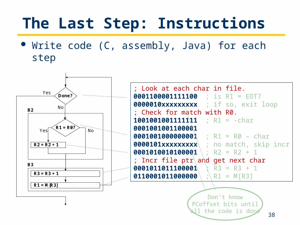
The Last Step: Instructions Write code (C, assembly, Java) for each step
R1 = M[R3]
Done?
No
Yes
B2
B3
R3 = R3 + 1
R1 = R0?
R2 = R2 + 1
NoYes
; Look at each char in file.0001100001111100 ; is R1 = EOT?0000010xxxxxxxxx ; if so, exit loop; Check for match with R0.1001001001111111 ; R1 = -char00010010011000010001001000000001 ; R1 = R0 – char0000101xxxxxxxxx ; no match, skip incr0001010010100001 ; R2 = R2 + 1; Incr file ptr and get next char0001011011100001 ; R3 = R3 + 10110001011000000 ; R1 = M[R3]
Don’t knowPCoffset bits until
all the code is done

39
Types of Errors in Code Syntax Errors
– You made a typing error that resulted in an illegal operation.– Not usually an issue with machine language,
because almost any bit pattern corresponds tosome legal instruction.
– In high-level languages, these are often caught during thetranslation from language to machine code.
Logic Errors– Your program is legal, but wrong, so
the results don’t match the problem statement.– Trace the program to see what’s really happening and
determine how to get the proper behavior.
Data Errors– Input data is different than what you expected.– Test the program with a wide variety of inputs.

Instruction Set Architecture
41
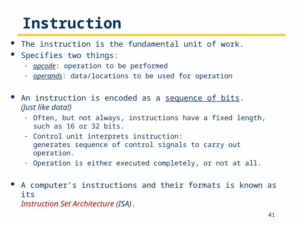
Instruction The instruction is the fundamental unit of work. Specifies two things:
– opcode: operation to be performed– operands: data/locations to be used for operation
An instruction is encoded as a sequence of bits. (Just like data!)
– Often, but not always, instructions have a fixed length,such as 16 or 32 bits.
– Control unit interprets instruction:generates sequence of control signals to carry out operation.
– Operation is either executed completely, or not at all.
A computer’s instructions and their formats is known as itsInstruction Set Architecture (ISA).
42
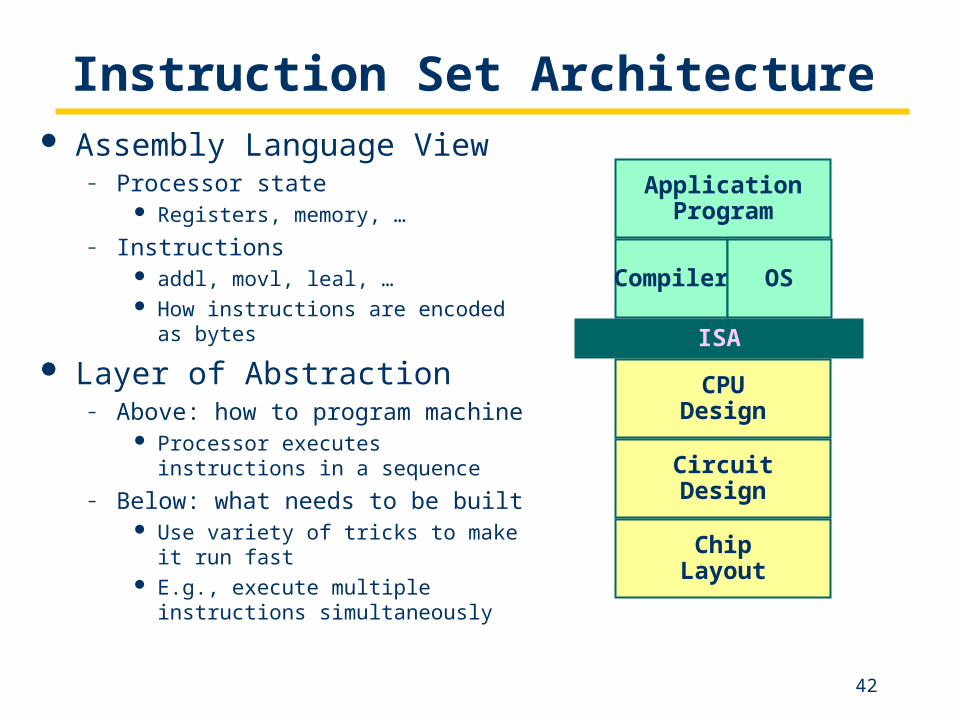
Instruction Set Architecture Assembly Language View
– Processor state Registers, memory, …
– Instructions addl, movl, leal, … How instructions are encoded as bytes
Layer of Abstraction– Above: how to program machine
Processor executes instructions in a sequence
– Below: what needs to be built Use variety of tricks to make it run fast E.g., execute multiple instructions
simultaneously
ISA
Compiler OS
CPUDesign
CircuitDesign
ChipLayout
ApplicationProgram
43
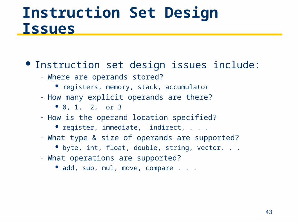
Instruction Set Design Issues
Instruction set design issues include:– Where are operands stored?
registers, memory, stack, accumulator
– How many explicit operands are there? 0, 1, 2, or 3
– How is the operand location specified? register, immediate, indirect, . . .
– What type & size of operands are supported? byte, int, float, double, string, vector. . .
– What operations are supported? add, sub, mul, move, compare . . .
44
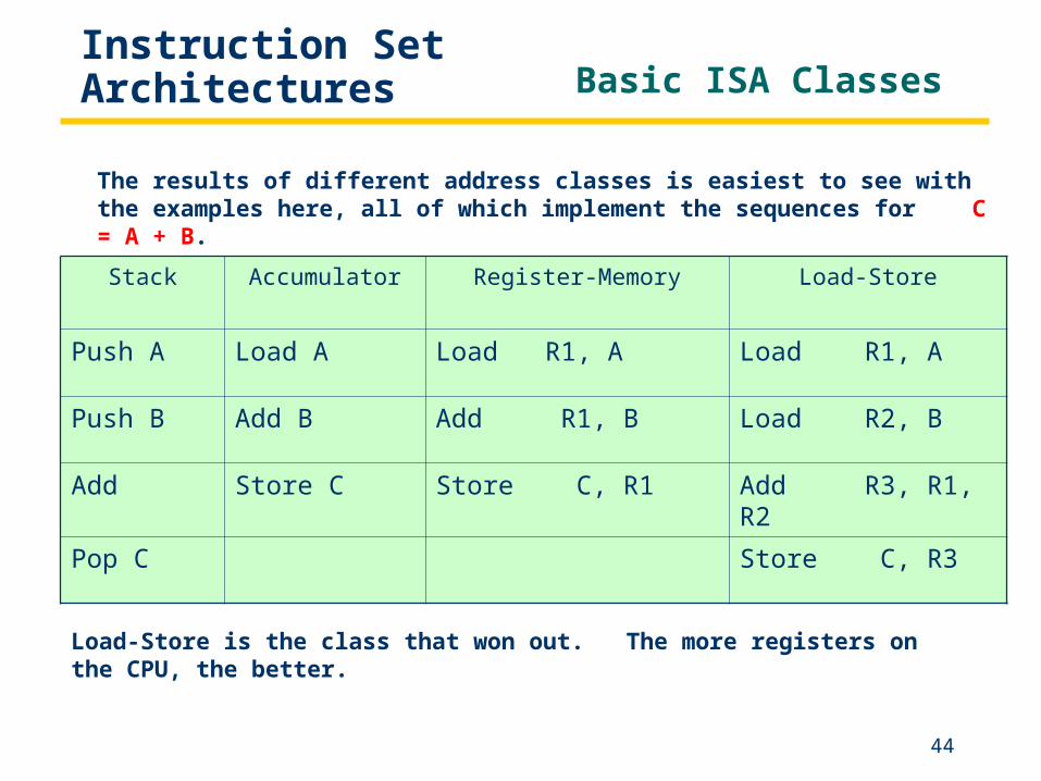
Instruction Set Architectures Basic ISA Classes
Stack Accumulator Register-Memory Load-Store
Push A Load A Load R1, A Load R1, A
Push B Add B Add R1, B Load R2, B
Add Store C Store C, R1 Add R3, R1, R2
Pop C Store C, R3
The results of different address classes is easiest to see with the examples here, all of which implement the sequences for C = A + B.
Load-Store is the class that won out. The more registers on the CPU, the better.

45
Types of Addressing Modes
Addressing Mode Example Action
1. Register Add R4, R3 R4 <- R4 + R3
2. Immediate Add R4, #3 R4 <- R4 + 3
3. Displacement Add R4, 100(R1) R4 <- R4 + M[100 + R1]
4. Register indirect Add R4, (R1) R4 <- R4 + M[R1]
5. Indexed Add R4, (R1 + R2) R4 <- R4 + M[R1 + R2]
6. Direct or absolute Add R4, (1000) R4 <- R4 + M[1000]
7. Memory Indirect Add R4, @(R3) R4 <- R4 + M[M[R3]]
8. Autoincrement Add R4, (R2)+ R4 <- R4 + M[R2]
R2 <- R2 + d
9. Autodecrement Add R4, (R2)- R4 <- R4 + M[R2]
R2 <- R2 - d
10. Scaled Add R4, 100(R2)[R3] R4 <- R4 +
M[100 + R2 + R3*d] Modes 1-4 account for 93% of all operands
46
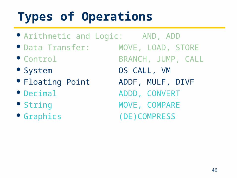
Types of Operations Arithmetic and Logic: AND, ADD Data Transfer: MOVE, LOAD, STORE Control BRANCH, JUMP, CALL System OS CALL, VM Floating Point ADDF, MULF, DIVF Decimal ADDD, CONVERT String MOVE, COMPARE Graphics (DE)COMPRESS
47
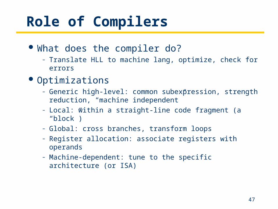
Role of Compilers
What does the compiler do?– Translate HLL to machine lang, optimize, check for errors
Optimizations– Generic high-level: common subexpression, strength reduction,
“machine independent”– Local: within a straight-line code fragment (a “block”)– Global: cross branches, transform loops– Register allocation: associate registers with operands– Machine-dependent: tune to the specific architecture (or ISA)
48
Role of Compilers (cont’d)
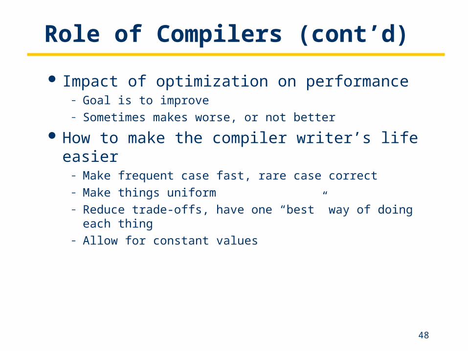
Impact of optimization on performance– Goal is to improve– Sometimes makes worse, or not better
How to make the compiler writer’s life easier– Make frequent case fast, rare case correct– Make things uniform– Reduce trade-offs, have one “best” way of doing each thing– Allow for constant values
49
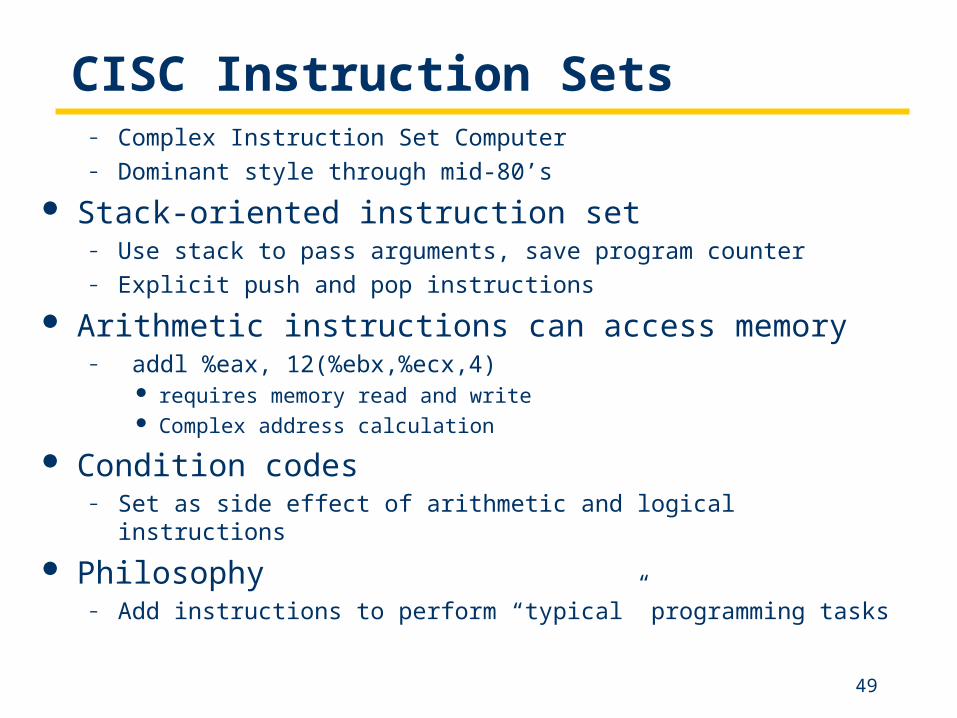
CISC Instruction Sets– Complex Instruction Set Computer– Dominant style through mid-80’s
Stack-oriented instruction set– Use stack to pass arguments, save program counter– Explicit push and pop instructions
Arithmetic instructions can access memory– addl %eax, 12(%ebx,%ecx,4)
requires memory read and write Complex address calculation
Condition codes– Set as side effect of arithmetic and logical instructions
Philosophy– Add instructions to perform “typical” programming tasks

50
RISC Instruction Sets– Reduced Instruction Set Computer– Internal project at IBM, later popularized by Hennessy (Stanford) and
Patterson (Berkeley)
Fewer, simpler instructions– Might take more to get given task done– Can execute them with small and fast hardware
Register-oriented instruction set– Many more (typically 32) registers– Use for arguments, return pointer, temporaries
Only load and store instructions can access memory– Similar to Y86 mrmovl and rmmovl
No Condition codes– Test instructions return 0/1 in register
51
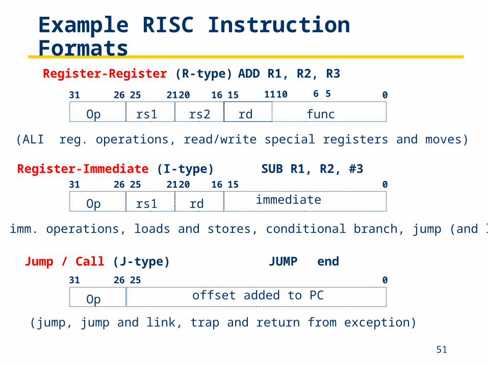
Example RISC Instruction Formats
Op
31 26 01516202125
rs1 rd immediate
Op
31 26 025
Op
31 26 01516202125
rs1 rs2
offset added to PC
rd
Register-Register (R-type) ADD R1, R2, R3
561011
Register-Immediate (I-type) SUB R1, R2, #3
Jump / Call (J-type) JUMP end
func
(ALU imm. operations, loads and stores, conditional branch, jump (and link)
(jump, jump and link, trap and return from exception)
(ALI reg. operations, read/write special registers and moves)
52
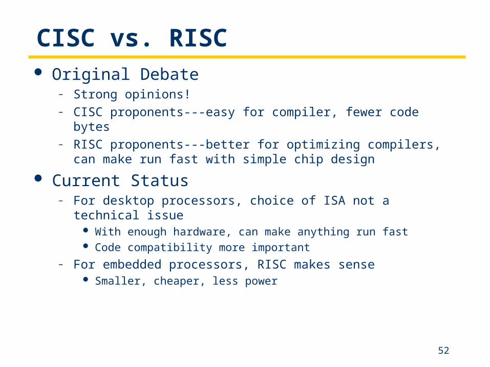
CISC vs. RISC Original Debate
– Strong opinions!– CISC proponents---easy for compiler, fewer code bytes– RISC proponents---better for optimizing compilers, can make run fast
with simple chip design
Current Status– For desktop processors, choice of ISA not a technical issue
With enough hardware, can make anything run fast Code compatibility more important
– For embedded processors, RISC makes sense Smaller, cheaper, less power
Sequential Processors
54
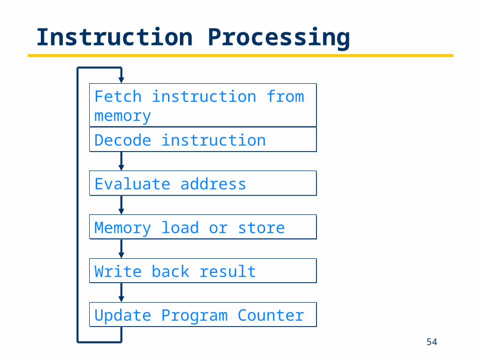
Instruction Processing
Decode instructionDecode instruction
Evaluate addressEvaluate address
Memory load or storeMemory load or store
Write back resultWrite back result
Update Program CounterUpdate Program Counter
Fetch instruction from memoryFetch instruction from memory
55
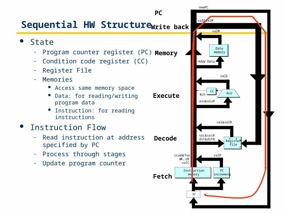
Sequential HW Structure
State– Program counter register (PC)– Condition code register (CC)– Register File– Memories
Access same memory space Data: for reading/writing program data Instruction: for reading instructions
Instruction Flow– Read instruction at address specified by
PC– Process through stages– Update program counter
Instructionmemory
Instructionmemory
PCincrement
PCincrement
CCCCALUALU
Datamemory
Datamemory
Fetch
Decode
Execute
Memory
Write back
icode, ifunrA , rB
valC
Registerfile
Registerfile
A BM
E
Registerfile
Registerfile
A BM
E
PC
valP
srcA, srcBdstA, dstB
valA, valB
aluA, aluB
Bch
valE
Addr, Data
valM
PCvalE, valM
newPC
56
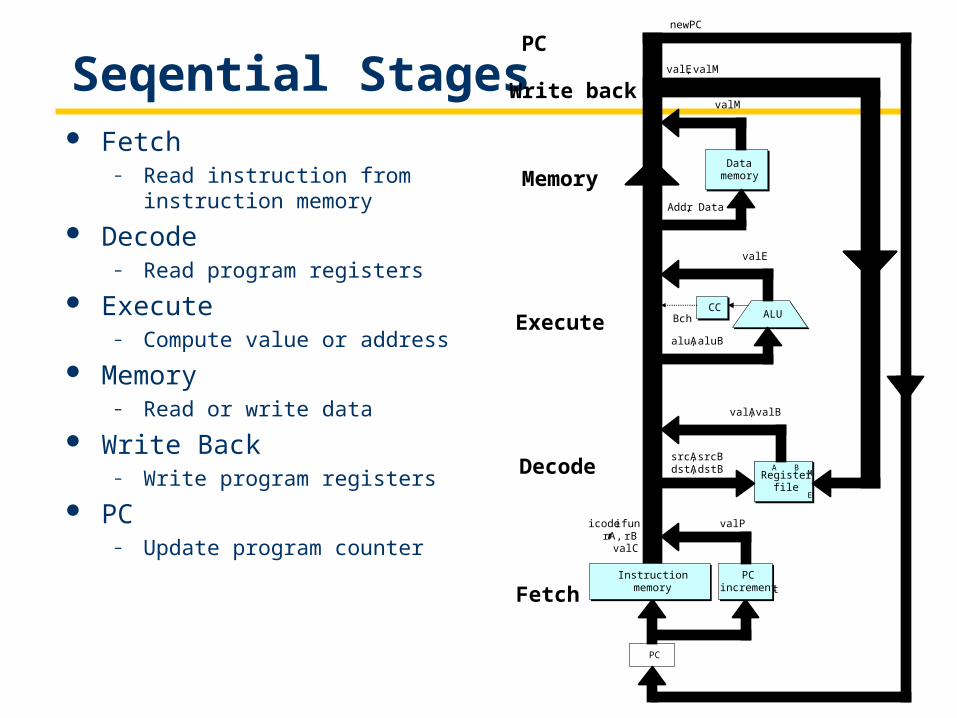
Seqential Stages Fetch
– Read instruction from instruction memory
Decode– Read program registers
Execute– Compute value or address
Memory– Read or write data
Write Back– Write program registers
PC– Update program counter
Instructionmemory
Instructionmemory
PCincrement
PCincrement
CCCCALUALU
Datamemory
Datamemory
Fetch
Decode
Execute
Memory
Write back
icode, ifunrA , rB
valC
Registerfile
Registerfile
A BM
E
Registerfile
Registerfile
A BM
E
PC
valP
srcA, srcBdstA, dstB
valA, valB
aluA, aluB
Bch
valE
Addr, Data
valM
PCvalE, valM
newPC

57
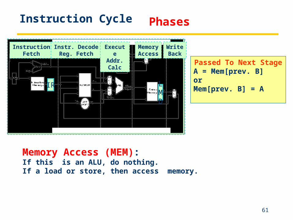
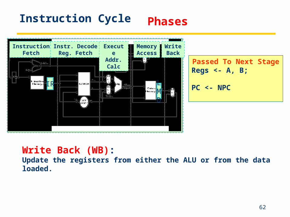
Phases
MemoryAccess
WriteBack
InstructionFetch
Instr. DecodeReg. Fetch
ExecuteAddr. Calc
IR LMD
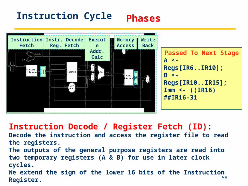
Instruction Fetch (IF):Send out the PC and fetch the instruction from memory into the instruction register (IR); increment the PC by 4 to address the next sequential instruction.IR holds the instruction that will be used in the next stage.NPC holds the value of the next PC.
Passed To Next StageIR <- Mem[PC]NPC <- PC + 4
Instruction Cycle
58
Phases
MemoryAccess
WriteBack
InstructionFetch
Instr. DecodeReg. Fetch
ExecuteAddr. Calc
IR LMD
Instruction Decode / Register Fetch (ID):Decode the instruction and access the register file to read the registers.The outputs of the general purpose registers are read into two temporary registers (A & B) for use in later clock cycles.We extend the sign of the lower 16 bits of the Instruction Register.
Passed To Next Stage A <- Regs[IR6..IR10];B <- Regs[IR10..IR15];Imm <- ((IR16) ##IR16-31
Instruction Cycle

59
Instruction Decoding
Instruction Format– Instruction byte icode:ifun– Optional register byte rA:rB– Optional constant word valC
5 0 rA rB D
icodeifun
rArB
valC
Optional Optional
60
Phases
MemoryAccess
WriteBack
InstructionFetch
Instr. DecodeReg. Fetch
ExecuteAddr. Calc
IR LMD
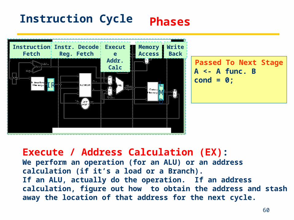
Passed To Next StageA <- A func. Bcond = 0;
Execute / Address Calculation (EX):We perform an operation (for an ALU) or an address calculation (if it’s a load or a Branch).If an ALU, actually do the operation. If an address calculation, figure out how to obtain the address and stash away the location of that address for the next cycle.
Instruction Cycle
61
Phases
MemoryAccess
WriteBack
InstructionFetch
Instr. DecodeReg. Fetch
ExecuteAddr. Calc
IR LMD
Passed To Next StageA = Mem[prev. B]orMem[prev. B] = A
Memory Access (MEM):If this is an ALU, do nothing.If a load or store, then access memory.
Instruction Cycle
62
Phases
MemoryAccess
WriteBack
InstructionFetch
Instr. DecodeReg. Fetch
ExecuteAddr. Calc
IR LMD
Passed To Next StageRegs <- A, B;
PC <- NPC
Write Back (WB):Update the registers from either the ALU or from the data loaded.
Instruction Cycle
63
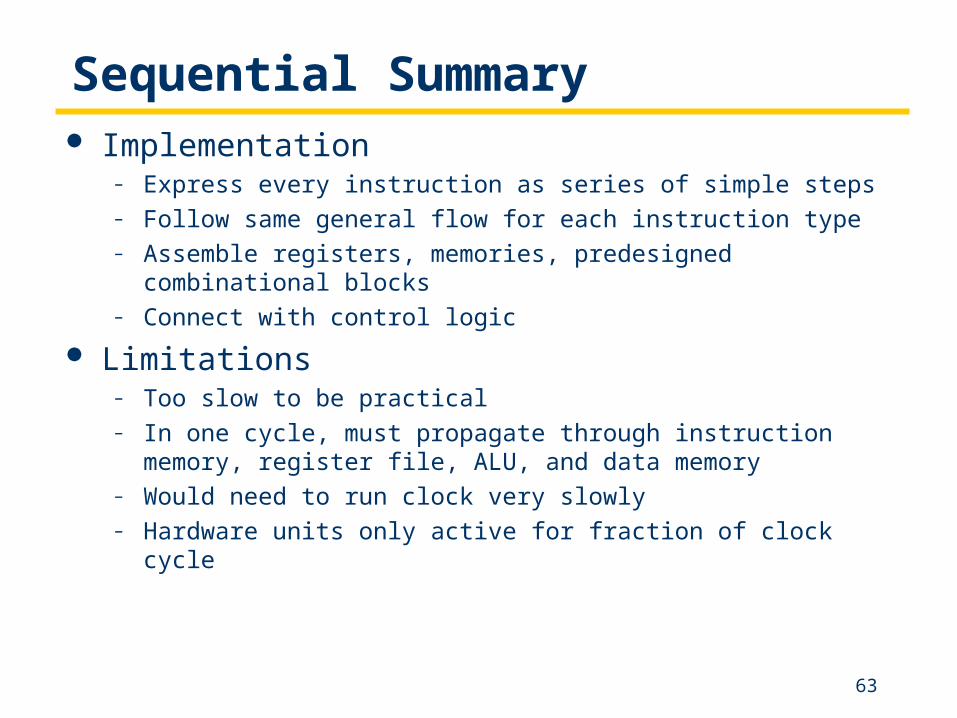
Sequential Summary Implementation
– Express every instruction as series of simple steps– Follow same general flow for each instruction type– Assemble registers, memories, predesigned combinational blocks– Connect with control logic
Limitations– Too slow to be practical– In one cycle, must propagate through instruction memory, register file,
ALU, and data memory– Would need to run clock very slowly– Hardware units only active for fraction of clock cycle

Pipelined Processors

65
What is Pipelining Computers execute billions of instructions, so instruction
throughput is what matters IDEA: Divide instruction execution up into several pipeline
stages. For example
IF ID EX MEM WB Simultaneously have different instructions in different
pipeline stages The length of the longest pipeline stage determines the
cycle time Desirable pipeline features (e.g., RISC):
– all instructions same length– registers located in same place in instruction format– memory operands only in loads or stores

66
What Is Pipelining
Laundry Example
Ann, Brian, Cathy, Dave each have one load of clothes to wash, dry, and fold
Washer takes 30 minutes
Dryer takes 40 minutes
“Folder” takes 20 minutes
A B C D

67
What Is Pipelining
Sequential laundry takes 6 hours for 4 loads
If they learned pipelining, how long would laundry take?
A
B
C
D
30 40 20 30 40 20 30 40 20 30 40 20
6 PM 7 8 9 10 11 Midnight
Task
Order
Time

68
Start work ASAP
Pipelined laundry takes 3.5 hours for 4 loads A
B
C
D
6 PM 7 8 9 10 11 Midnight
Task
Order
Time
30 40 40 40 40 20
What Is Pipelining
69
Pipelining Lessons
Pipelining doesn’t help latency of single task, it helps throughput of entire workload
Pipeline rate limited by slowest pipeline stage
Multiple tasks operating simultaneously
Potential speedup = Number pipe stages
Unbalanced lengths of pipe stages reduces speedup
Time to “fill” pipeline and time to “drain” it reduces speedup
A
B
C
D
6 PM 7 8 9
Task
Order
Time
30 40 40 40 40 20
What Is Pipelining

70
Real-World Pipelines: Car Washes
Idea– Divide process into independent stages– Move objects through stages in sequence– At any given time, multiple objects being processed
Sequential Parallel
Pipelined

71
Pipeline Diagrams Unpipelined
– Cannot start new operation until previous one completes
3-Way Pipelined
– Up to 3 operations in process simultaneously
Time
OP1
OP2
OP3
Time
A B C
A B C
A B C
OP1
OP2
OP3
72
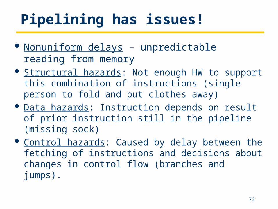
Pipelining has issues!
Nonuniform delays – unpredictable reading from memory
Structural hazards: Not enough HW to support this combination of instructions (single person to fold and put clothes away)
Data hazards: Instruction depends on result of prior instruction still in the pipeline (missing sock)
Control hazards: Caused by delay between the fetching of instructions and decisions about changes in control flow (branches and jumps).

73
Data Dependencies
System– Each operation depends on result from preceding one
Clock
Combinationallogic
Reg
Time
OP1
OP2
OP3

74
Data Hazards
– Result does not feed back around in time for next operation– Pipelining has changed behavior of system
Reg
Clock
Comb.logic
A
Reg
Comb.logic
B
Reg
Comb.logic
C
Time
OP1
OP2
OP3
A B C
A B C
A B C
OP4 A B C
75
One Memory Port/Structural Hazards
Instr.
Order
Time (clock cycles)
Load
Instr 1
Instr 2
Instr 3
Instr 4
Reg
ALU
DMemIfetch Reg
Reg
ALU
DMemIfetch Reg
Reg
ALU
DMemIfetch Reg
Reg
ALU
DMemIfetch Reg
Cycle 1Cycle 2 Cycle 3Cycle 4 Cycle 6Cycle 7Cycle 5
Reg
ALU
DMemIfetch Reg

76
Read After Write (RAW) InstrJ tries to read operand before InstrI writes it
Caused by a “Dependence” (in compiler nomenclature). This hazard results from an actual need for communication.
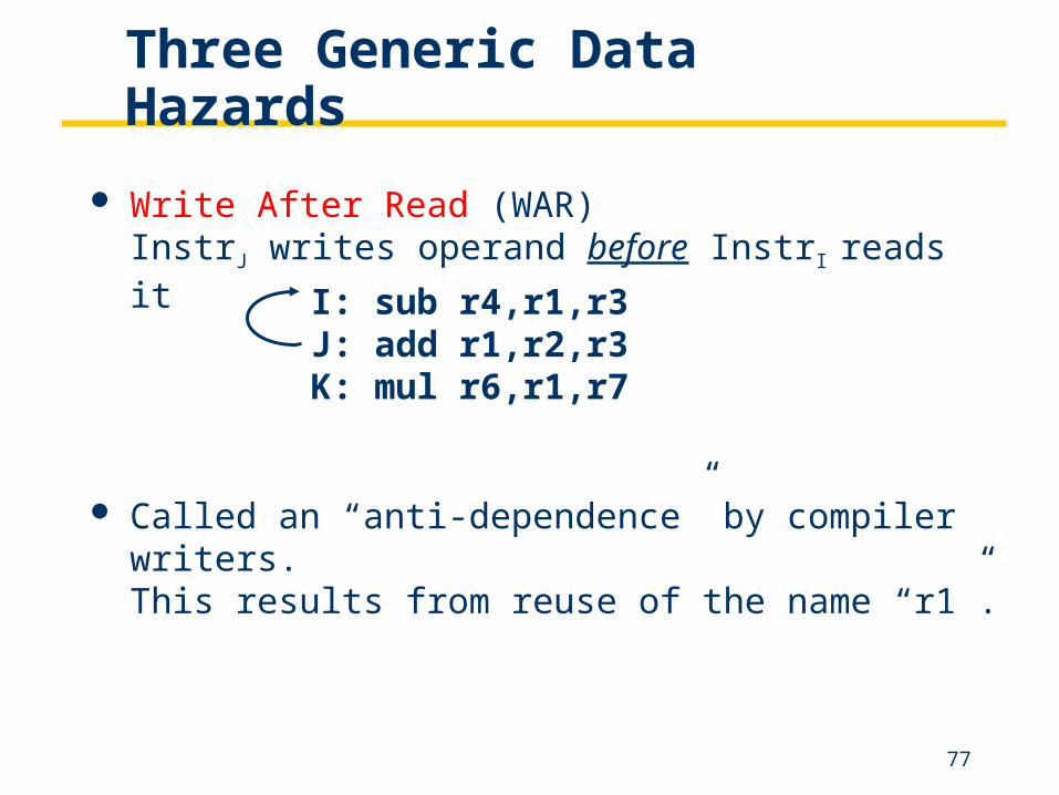
Three Generic Data Hazards
I: add r1,r2,r3J: sub r4,r1,r3
77
Write After Read (WAR) InstrJ writes operand before InstrI reads it
Called an “anti-dependence” by compiler writers.This results from reuse of the name “r1”.
I: sub r4,r1,r3 J: add r1,r2,r3K: mul r6,r1,r7
Three Generic Data Hazards
78
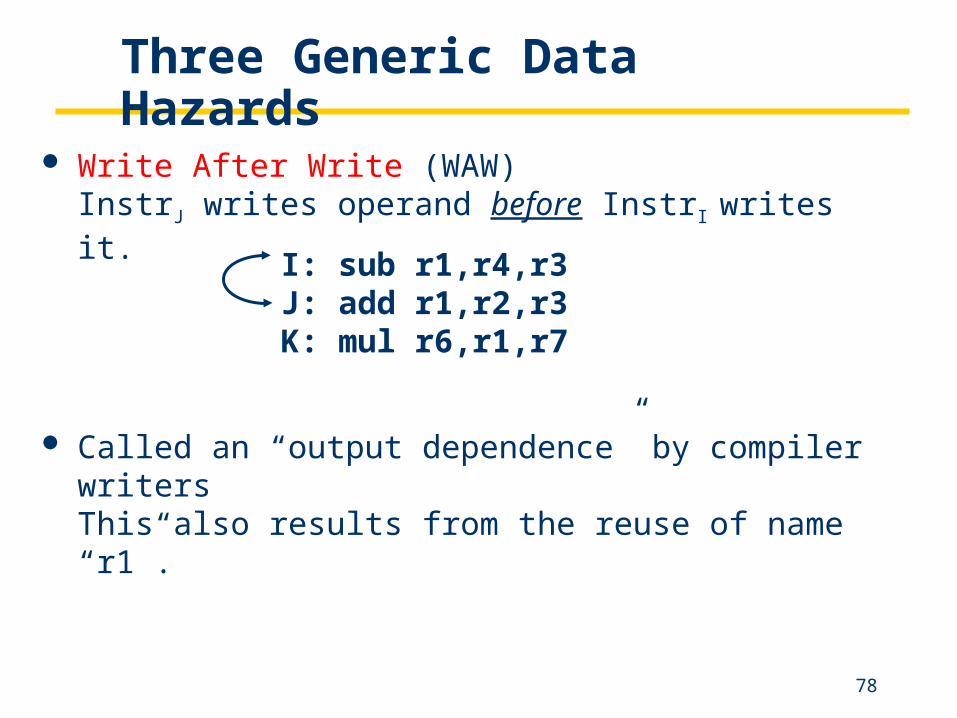
Three Generic Data Hazards
Write After Write (WAW) InstrJ writes operand before InstrI writes it.
Called an “output dependence” by compiler writersThis also results from the reuse of name “r1”.
I: sub r1,r4,r3 J: add r1,r2,r3K: mul r6,r1,r7

79
Control Hazards
10: beq r1,r3,36
14: and r2,r3,r5
18: or r6,r1,r7
22: add r8,r1,r9
36: xor r10,r1,r11
Reg ALU
DMemIfetch Reg
Reg
ALU
DMemIfetch Reg
Reg
ALU
DMemIfetch Reg
Reg
ALU
DMemIfetch Reg
Reg
ALU
DMemIfetch Reg
What do you do with the 3 instructions in between?
80
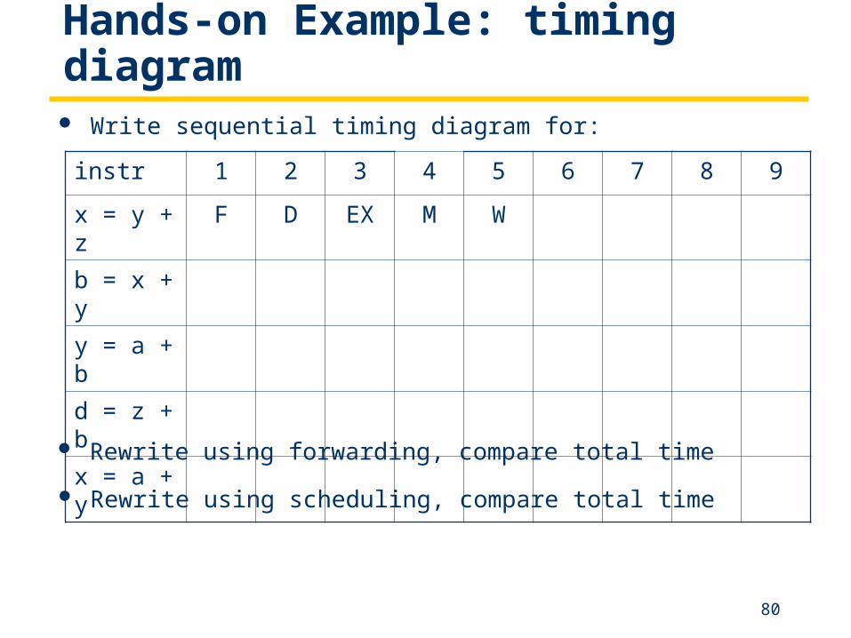
Hands-on Example: timing diagram Write sequential timing diagram for:
instr 1 2 3 4 5 6 7 8 9
x = y + z F D EX M W
b = x + y
y = a + b
d = z + b
x = a + y
Rewrite using forwarding, compare total time
Rewrite using scheduling, compare total time
Related Documents