http://www.cirrus.com Copyright Cirrus Logic, Inc. 2009 (All Rights Reserved) CS3011 CS3012 Precision Low-voltage Amplifier; DC to 1 kHz Features & Description Low Offset: 10 μV Max Low Drift: 0.05 μV/°C Max Low Noise – 12 nV/√Hz @ 0.5 Hz – 0.1 to 10 Hz = 250 nVp-p – 1/f corner @ 0.08 Hz Open-loop Voltage Gain – 300 dB Typ – 200 dB Min Rail-to-rail Output Swing Slew Rate: 2 V/μs Applications Thermocouple/Thermopile Amplifiers Load Cell and Bridge Transducer Amplifiers Precision Instrumentation Battery-powered Systems Description The CS3011 single amplifier and the CS3012 dual am- plifier are designed for precision amplification of low- level signals and are ideally suited to applications that require very high closed-loop gains. These amplifiers achieve excellent offset stability, super-high open-loop gain, and low noise over time and temperature. The de- vices also exhibit excellent CMRR and PSRR. The common mode input range includes the negative supply rail. The amplifiers operate with any total supply voltage from 2.7 V to 6.7 V (±1.35 V to ±3.35 V). Pin Configurations PDWN -In +In V- NC V+ Output NC - + 1 2 3 4 8 7 6 5 Out A -In A +In A V- V+ Out B -In B +In B A B - - + + 1 2 3 4 8 7 6 5 CS3011 8-lead SOIC CS3012 8-lead SOIC 1 10 100 0.001 0.010 0.1 1 10 Frequency (Hz) nV/√Hz Noise vs. Frequency (Measured) CS3011 R1 100 R2 64.9k C1 0.015μF Dexter Research Thermopile ST60 JUL ‘09 DS597F6

Welcome message from author
This document is posted to help you gain knowledge. Please leave a comment to let me know what you think about it! Share it to your friends and learn new things together.
Transcript
http://www.cirrus.comCopyright Cirrus Logic, Inc. 2009
(All Rights Reserved)
CS3011CS3012
Precision Low-voltage Amplifier; DC to 1 kHzFeatures & DescriptionLow Offset: 10 μV MaxLow Drift: 0.05 μV/°C MaxLow Noise
– 12 nV/√Hz @ 0.5 Hz– 0.1 to 10 Hz = 250 nVp-p– 1/f corner @ 0.08 Hz
Open-loop Voltage Gain– 300 dB Typ– 200 dB Min
Rail-to-rail Output SwingSlew Rate: 2 V/μs
ApplicationsThermocouple/Thermopile AmplifiersLoad Cell and Bridge Transducer AmplifiersPrecision InstrumentationBattery-powered Systems
DescriptionThe CS3011 single amplifier and the CS3012 dual am-plifier are designed for precision amplification of low-level signals and are ideally suited to applications thatrequire very high closed-loop gains. These amplifiersachieve excellent offset stability, super-high open-loopgain, and low noise over time and temperature. The de-vices also exhibit excellent CMRR and PSRR. Thecommon mode input range includes the negative supplyrail. The amplifiers operate with any total supply voltagefrom 2.7 V to 6.7 V (±1.35 V to ±3.35 V).
Pin Configurations
PDWN
-In
+In
V-
NC
V+
Output
NC
-
+
1
2
3
4
8
7
6
5
Out A
-In A
+In A
V-
V+
Out B
-In B
+In B
A
B-
-
+
+
1
2
3
4
8
7
6
5
CS3011
8-lead SOIC
CS3012
8-lead SOIC
1
10
100
0.001 0.010 0.1 1 10
Frequency (Hz)
nV
/√H
z
Noise vs. Frequency (Measured)CS3011
R1100
R264.9k
C10.015μF
Dexter ResearchThermopile ST60
JUL ‘09DS597F6
CS3011CS3012
2 DS597F6
TABLE OF CONTENTS
1. CHARACTERISTICS AND SPECIFICATIONS .................................................... 32. TYPICAL PERFORMANCE PLOTS ..................................................................... 43. CS3011/CS3012 OVERVIEW ............................................................................... 8
3.1 Open Loop Gain and Phase Response ......................................................................93.2 Open Loop Gain and Stability Compensation ...........................................................10
3.2.1 Discussion ................................................................................................103.2.2 Gain Calculations Summary and Recommendations .. .............................13
3.3 Powerdown (PDWN) .................................................................................................133.4 Applications ..............................................................................................................14
4. ORDERING INFORMATION .............................................................................. 155. ENVIRONMENTAL, MANUFACTURING, & HANDLING INFORMATION ........ 156. PACKAGE DRAWING ........................................................................................ 167. REVISION HISTORY ......................................................................................... 17
LIST OF FIGURES
Figure 1. Noise vs. Frequency (Measured) ................................................................ 4Figure 2. 0.01 Hz to 10 Hz Noise ............................................................................... 4Figure 3. Supply Current vs. Temperature, 3011 ....................................................... 4Figure 4. Noise vs. Frequency ................................................................................... 4Figure 5. Offset Voltage Stability (DC to 3.2 Hz) ........................................................ 4Figure 6. Supply Current vs. Temperature, 3012 ....................................................... 4Figure 7. Supply Current vs. Voltage, 3011 ............................................................... 5Figure 8. Supply Current vs. Voltage, 3012 ............................................................... 5Figure 9. Open Loop Gain and Phase vs Frequency ................................................. 5Figure 10. Open Loop Gain and Phase vs Frequency (Expanded) ........................... 6Figure 11. Input Bias Current vs Common Mode Voltage (CS3012) ......................... 6Figure 12. Voltage Swing vs. Output Current (2.7 V) ................................................. 7Figure 13. Voltage Swing vs. Output Current (5 V) .................................................... 7Figure 14. CS3011/CS3012 Open Loop Gain and Phase Response ........................ 9Figure 15. Non-Inverting Gain Configuration ........................................................... 10Figure 16. Non-Inverting Gain Configuration with Compensation ............................ 11Figure 17. Loop Gain Plot: Unity Gain and with Pole-Zero Compensation .............. 12Figure 18. Thermopile Amplifier with a Gain of 650 V/V .......................................... 14Figure 19. Load Cell Bridge Amplifier and A/D Converter ........................................ 14Figure 20.
CS3011CS3012
DS597F6 3
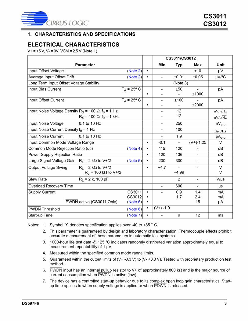
1. CHARACTERISTICS AND SPECIFICATIONS
ELECTRICAL CHARACTERISTICSV+ = +5 V, V- = 0V, VCM = 2.5 V (Note 1)
Notes: 1. Symbol “•” denotes specification applies over -40 to +85 ° C. 2. This parameter is guaranteed by design and laboratory characterization. Thermocouple effects prohibit
accurate measurement of these parameters in automatic test systems.3. 1000-hour life test data @ 125 °C indicates randomly distributed variation approximately equal to
measurement repeatability of 1 µV.4. Measured within the specified common mode range limits.5. Guaranteed within the output limits of (V+ -0.3 V) to (V- +0.3 V). Tested with proprietary production test
method.6. PWDN input has an internal pullup resistor to V+ of approximately 800 kΩ and is the major source of
current consumption when PWDN is active (low).7. The device has a controlled start-up behavior due to its complex open loop gain characteristics. Start-
up time applies to when supply voltage is applied or when PDWN is released.
ParameterCS3011/CS3012
UnitMin Typ MaxInput Offset Voltage (Note 2) • - - ±10 µVAverage Input Offset Drift (Note 2) • - ±0.01 ±0.05 µV/ºCLong Term Input Offset Voltage Stability (Note 3)Input Bias Current TA = 25º C
•--
±50-
-±1000
pA
Input Offset Current TA = 25º C•
--
±100-
-±2000
pA
Input Noise Voltage Density RS = 100 Ω, f0 = 1 HzRS = 100 Ω, f0 = 1 kHz
--
1212
Input Noise Voltage 0.1 to 10 Hz - 250 nVp-pInput Noise Current Density f0 = 1 Hz - 100
Input Noise Current 0.1 to 10 Hz - 1.9 pAp-pInput Common Mode Voltage Range • -0.1 - (V+)-1.25 VCommon Mode Rejection Ratio (dc) (Note 4) • 115 120 - dBPower Supply Rejection Ratio • 120 136 - dBLarge Signal Voltage Gain RL = 2 kΩ to V+/2 (Note 5) • 200 300 - dB
Output Voltage Swing RL = 2 kΩ to V+/2 RL = 100 kΩ to V+/2
• +4.7 -+4.99
- VV
Slew Rate RL = 2 k, 100 pF 2 - V/µs
Overload Recovery Time - 600 - µsSupply Current CS3011
CS3012 PWDN active (CS3011 Only) (Note 6)
•••
- 0.91.7
1.42.415
mAmAµA
PWDN Threshold (Note 6) • (V+) -1.0
Start-up Time (Note 7) • - 9 12 ms
nV/ Hz
nV/ Hz
fA/ Hz
CS3011CS3012
4 DS597F6
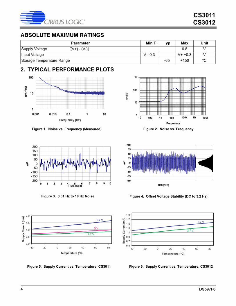
ABSOLUTE MAXIMUM RATINGS
2. TYPICAL PERFORMANCE PLOTS
Parameter Min T yp Max UnitSupply Voltage [(V+) - (V-)] 6.8 VInput Voltage V- -0.3 V+ +0.3 VStorage Temperature Range -65 +150 ºC
1
10
100
0.001 0.010 0.1 1 10
Frequency (Hz)
nV
/√H
z
Figure 1. Noise vs. Frequency (Measured)
Figure 3. 0.01 Hz to 10 Hz Noise
-200-150-100-50
050
100150200
TIME (Sec)
nV
TIME (Sec)0 1 2 3 4 5 6 7 8 9 10
Temperature (°C)
Sup
ply
Curr
ent(
mA)
2.7 V
6.7 V
5 V
0.0
0.5
1.0
1.5
2.0
-40 -20 0 20 40 60 80
Figure 5. Supply Current vs. Temperature, CS3011
1
10
100
1000
10 100 1000 10000 100000 1000000
1E+07
Freq uen cynV
/ Hz
Figure 2. Noise vs. Frequency
10
100
1k
110 100 1k 10k
Frequency
100k 1M 10M
Figure 4. Offset Voltage Stability (DC to 3.2 Hz)
-100
-75
-50
-25
0
25
50
75
100
TIME (1 HR)
nV
σ = 13 nV
0.50.70.91.11.31.51.71.9
-40 -20 0 20 40 60 80
Temperature (°C)
Supp
lyCu
rren
t(m
A)
2.7 V
6.7 V
Figure 6. Supply Current vs. Temperature, CS3012
CS3011CS3012
DS597F6 5
Typical Performance Plots (Cont.)
0.5
0.6
0.7
0.8
0.9
1
2 3 4 5 6 7
Supply Voltage (V)
Sup
ply
Curr
ent(
mA)
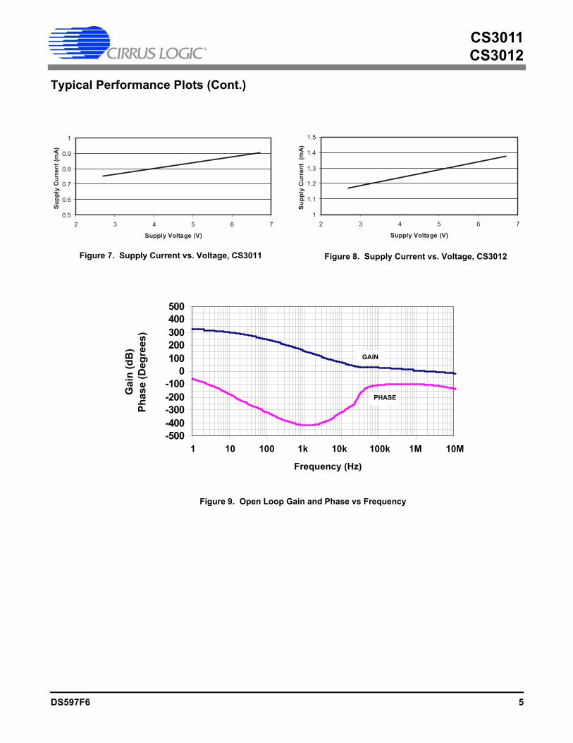
Figure 7. Supply Current vs. Voltage, CS3011
1
1.1
1.2
1.3
1.4
1.5
2 3 4 5 6 7
Supply Voltage (V)
Sup
ply
Curr
ent
(mA)
Figure 8. Supply Current vs. Voltage, CS3012
Figure 9. Open Loop Gain and Phase vs Frequency
100 K
-500-400-300-200-100
0100200300400500
1 10 100 1000 10000 100000 1000000
1E+07
Frequency (Hz)
Gai
n (d
B)
Ph
ase
(Deg
rees
)
1 10 100 1k 10k 1M 10M
Frequency (Hz)
100k
GAIN
PHASE
CS3011CS3012
6 DS597F6
Typical Performance Plots (Cont.)
0
20
40
60
80Ga
in (d
B)
-360
-315
-270
-225
-180
-135
-90
-45
0
10000 100000 1000000 10000000
Phas
e (d
egre
es)
0
10 K 100 K 1 M 10 M
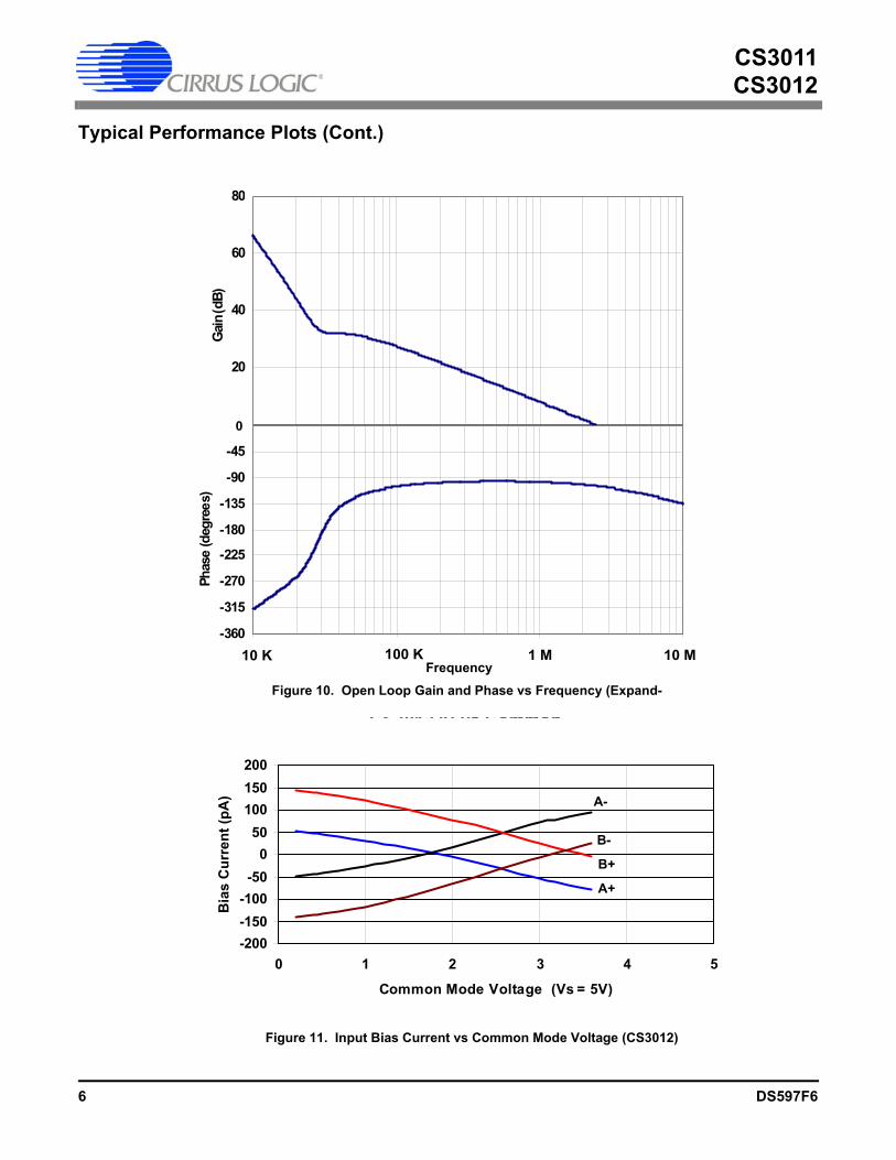
Figure 10. Open Loop Gain and Phase vs Frequency (Expand-Frequency
Figure 11. Input Bias Current vs Common Mode Voltage (CS3012)
CS3012 IB vs Common
-200-150-100-50
050
100150200
0 1 2 3 4 5
Common Mode Voltage (Vs = 5V)
Bia
s C
urre
nt (p
A) A-
A+
B-
B+
CS3011CS3012
DS597F6 7
Typical Performance Plots (Cont.)
-200
-150
-250
-100
-50
V+
V–
+50
+100
+150
+200
+250
0 1 2 3 4 5Output Current (mA)
Out
putV
olta
ge(m
V)
-40°C
+125°C
+25°C
+125°C
+25°C
-40°C
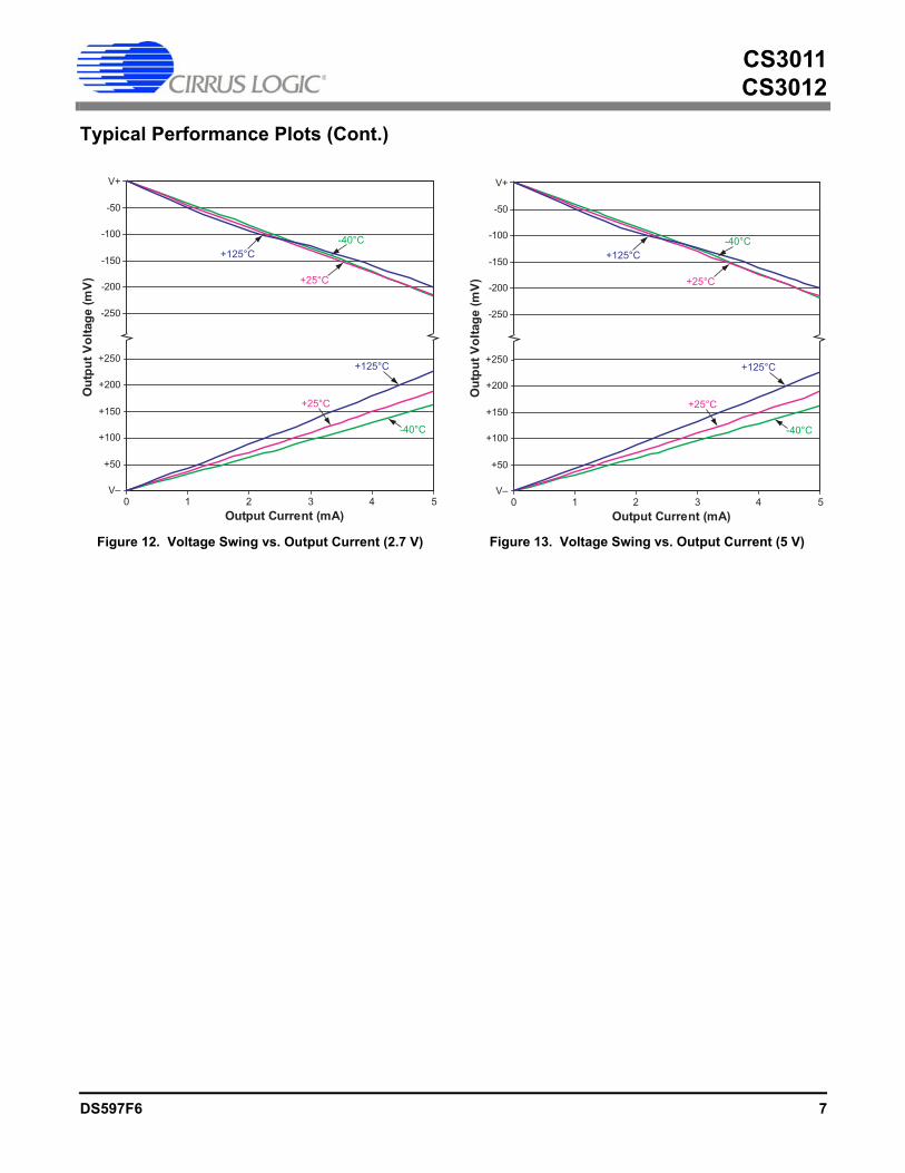
Figure 12. Voltage Swing vs. Output Current (2.7 V)
-200
-150
-250
-100
-50
V+
V–
+50
+100
+150
+200
+250
0 1 2 3 4 5Output Current (mA)
Out
putV
olta
ge(m
V)
-40°C
+125°C
+25°C
+125°C
+25°C
-40°C
Figure 13. Voltage Swing vs. Output Current (5 V)
CS3011CS3012
8 DS597F6
3. CS3011/CS3012 OVERVIEWThe CS3011/CS3012 amplifiers are designed forprecision measu rement o f sign als from DC to1 kHz when opera ting from a supply voltage of+2.7 V to +6.7 V (± 1.35 to ± 3.35 V). The amplifi-ers are designed with a patented architecture thatutilizes multiple amplifier stages to yield very highopen loop gain at frequencies of 1 kHz and below.The amplifiers yield low noise and low offset dr ift
while consuming relatively low supply current . Anincrease in noise floor above 1 kHz is the result ofintermediate stages of the amplifier being operatedat very low currents. The amplifiers are intende dfor amplifying small signals with large gains in ap-plications where the output of the amplifier can beband-limited to frequencies below 1 kHz.
CS3011CS3012
DS597F6 9
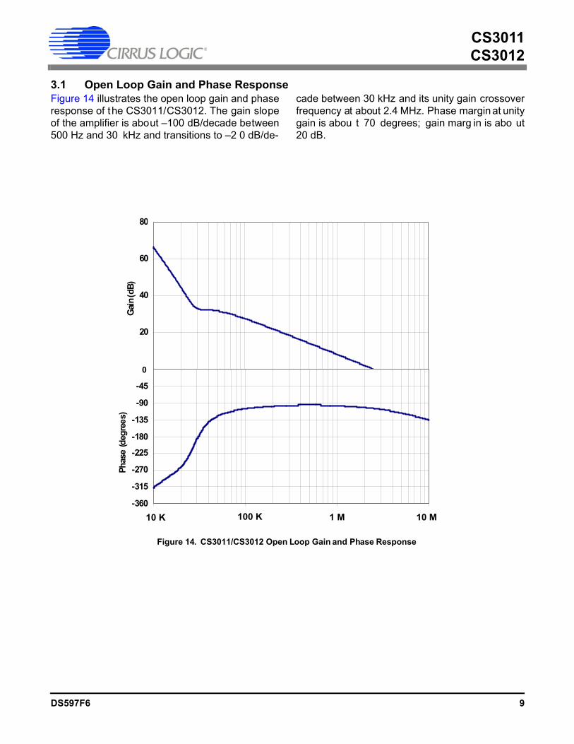
3.1 Open Loop Gain and Phase ResponseFigure 14 illustrates the open loop gain and phaseresponse of the CS3011/CS3012. The gain slopeof the amplifier is about –100 dB/decade between500 Hz and 30 kHz and transitions to –2 0 dB/de-
cade between 30 kHz and its unity gain crossoverfrequency at about 2.4 MHz. Phase margin at unitygain is abou t 70 degrees; gain marg in is abo ut20 dB.
Figure 14. CS3011/CS3012 Open Loop Gain and Phase Response
0
20
40
60
80
Gai
n (dB
)
-360
-315
-270
-225
-180
-135
-90
-45
0
10000 100000 1000000 10000000
Phas
e (d
egre
es)
0
10 K 100 K 1 M 10 M
CS3011CS3012
10 DS597F6
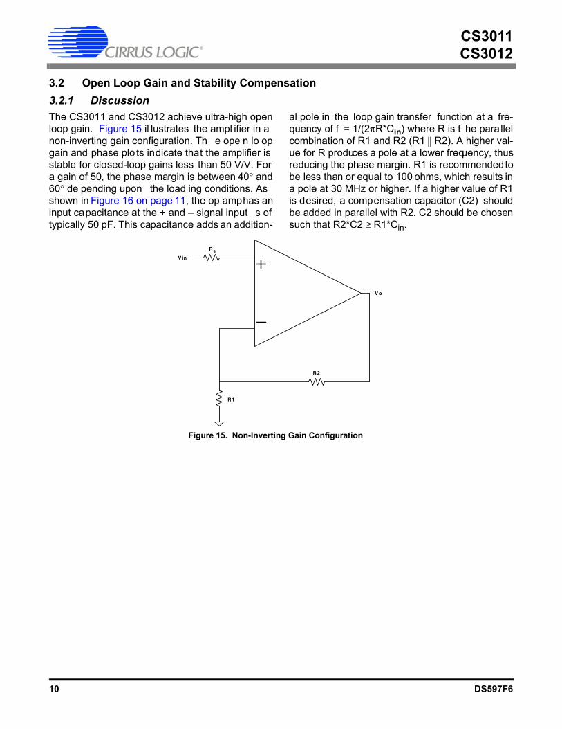
3.2 Open Loop Gain and Stability Compensation3.2.1 DiscussionThe CS3011 and CS3012 achieve ultra-high openloop gain. Figure 15 il lustrates the ampl ifier in anon-inverting gain configuration. Th e ope n lo opgain and phase plo ts indicate that the amplifier isstable for closed-loop gains less than 50 V/V. Fora gain of 50, the phase margin is between 40° and60° de pending upon the load ing conditions. Asshown in Figure 16 on page 11, the op amp has aninput capacitance at the + and – signal input s oftypically 50 pF. This capacitance adds an addition-
al pole in the loop gain transfer function at a fre-quency of f = 1/(2πR*Cin) where R is t he para llelcombination of R1 and R2 (R1 || R2). A higher val-ue for R produces a pole at a lower frequency, thusreducing the phase margin. R1 is recommended tobe less than or equal to 100 ohms, which results ina pole at 30 MHz or higher. If a higher value of R1is desired, a compensation capacitor (C2) shouldbe added in parallel with R2. C2 should be chosensuch that R2*C2 ≥ R1*Cin.
R1
R2
Vin
Vo
R S
Figure 15. Non-Inverting Gain Configuration
CS3011CS3012
DS597F6 11
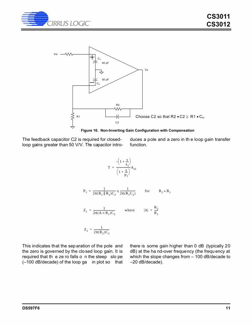
The feedback capacitor C2 is required for closed-loop gains greater than 50 V/V. The capacitor intro-
duces a pole and a zero in th e loop gain transferfunction.
This indicates that the separation of the pole andthe zero is governed by the closed loop gain. It isrequired that th e ze ro falls o n the steep slo pe(–100 dB/decade) of the loop ga in plot so that
there is some gain higher than 0 dB (typically 20dB) at the ha nd-over frequency (the frequ ency atwhich the slope changes from – 100 dB/decade to–20 dB/decade).
50 pF
50 pF
R1
R2
Vin
Vo
C2
Cin
Cin
Choose C2 so that R2 • C2 ≥ ?R1 • Cin
Figure 16. Non-Inverting Gain Configuration with Compensation
T
1 sz1-----+
–
1 sp1-----+
-----------------------Aol=
P11
2π R1 R2||( )C2------------------------------------- 1
2π R1C2( )-------------------------≅= for R2 R1»
Z11
2π A R1×( )C2-----------------------------------= where A
R2
R1------=
Z11
2π R2( )C2-------------------------=
CS3011CS3012
12 DS597F6
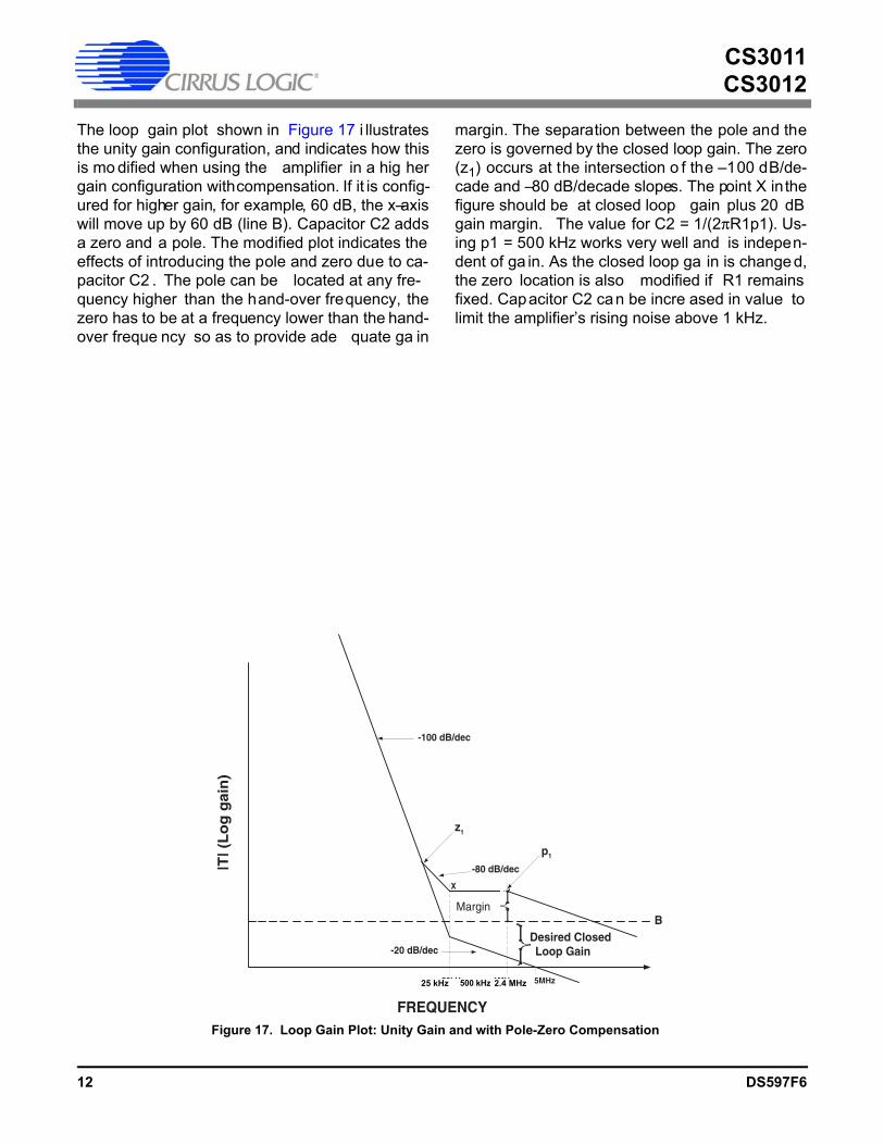
The loop gain plot shown in Figure 17 i llustratesthe unity gain configuration, and indicates how thisis mo dified when using the amplifier in a hig hergain configuration with compensation. If it is config-ured for higher gain, for example, 60 dB, the x–axiswill move up by 60 dB (line B). Capacitor C2 addsa zero and a pole. The modified plot indicates theeffects of introducing the pole and zero due to ca-pacitor C2 . The pole can be located at any fre-quency higher than the hand-over frequency, thezero has to be at a frequency lower than the hand-over freque ncy so as to provide ade quate ga in
margin. The separation between the pole and thezero is governed by the closed loop gain. The zero(z1) occurs at the intersection o f the –100 dB/de-cade and –80 dB/decade slopes. The point X in thefigure should be at closed loop gain plus 20 dBgain margin. The value for C2 = 1/(2πR1p1). Us-ing p1 = 500 kHz works very well and is indepen-dent of ga in. As the closed loop ga in is changed,the zero location is also modified if R1 remainsfixed. Capacitor C2 can be incre ased in value tolimit the amplifier’s rising noise above 1 kHz.
-100 dB/dec
|T| (
Lo
g g
ain
)
-80 dB/dec
z1
p1
Margin
-20 dB/dec
50kHz 1MHz 5MHz
Desired ClosedLoop Gain
X
FREQUENCY
B
Figure 17. Loop Gain Plot: Unity Gain and with Pole-Zero Compensation
2.4 MHz25 kHz 500 kHz
CS3011CS3012
DS597F6 13
3.2.2 Gain Calculations Summary and Recommendations
Condition #1: |Av| ≤ 50 and R1 ≤ 100 ΩThe Opamp is inherently stable for |Av| ≤ 50 andR1 ≤ 100 Ω . No C2 co mpensation cap acitoracross R2 is required.• |Av| = 1 config uration ha s 7 0° pha se margin
and 20 dB gain margin.• |Av| = 50 configuration ha s phase margin be-
tween 40° for C LOAD ≤ 100 pF and 60 ° forCLOAD = 0 pF.
Condition #2: |Av| ≤ 50 and R1 > 100 ΩCompensation capacitor C2 across R2 is required.Calculate C2 using the following formula:• C2 ≥ (R1 • Cin) / R2, where Cin = 50 pF
Condition #3: |Av| > 50Compensation capacitor C2 across R2 is required.Calculate and verify a value for C2 using the fol-lowing steps.
Calculate the Compensation Capacitor Value:1) Calculate a value for C2 using the following for-
mula:C2 = 1 / [2π (R1| |R2) • P1], where P1 = 1 MHz
To simplify the calculation, set the pole of the filterto P1 = 1 MHz. P1 must be set h igher than theopamp’s internal 50 kHz crossover frequency.2) Calculate a second value for C2 using the fol-
lowing formula:C2 ≥ (R1 • Cin) / R2, where Cin = 50 pF
3) Use the la rger of t he two va lues calculated insteps 1 & 2.
Verify the Opamp Compensation:Verify the opamp co mpensation using the ope n-loop gain and pha se resp onse Bode plot inFigure 14. Plot the calculated clo sed loop gaintransfer function and verify the following design cri-teria are met:• Pole P1 > opamp in ternal 50 kHz c rossover fre-
quency- P1 = 1 / [2π (R1| |R2) • C2], where P1 = 1 MHz- To sim plify the ca lculation, set t he p ole t o
P1 = 1 MHz.• Z1 < opamp internal 50 kHz crossover frequency
- Z1 = 1 / (2π R2 • C2)• Gain margin above the open-loop gain transfer
function is re quired. A g ain margin of +20 dBabove the open loop g ain transfer function isoptimal.
3.3 Powerdown (PDWN) The CS3011 single amplifier provides a power-down function on pin 1. If this pin is left ope n theamplifier will operate normally. If the powerdown isasserted low, the amplifier enters a powered downstate. Th ere is a pu ll-up resistor (approximately800 k ohm) inside the amplifier from pin 1 to the V+supply. The current through this pull-up resistor isthe main source of current drain in the powerdownstate.
CS3011CS3012
14 DS597F6
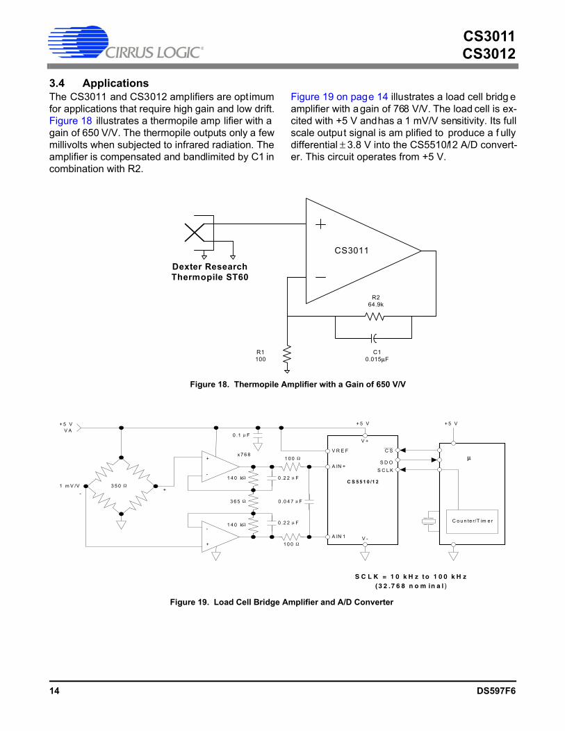
3.4 ApplicationsThe CS3011 and CS3012 amplifiers are opt imumfor applications that require high gain and low drift.Figure 18 illustrates a thermopile amp lifier with again of 650 V/V. The thermopile outputs only a fewmillivolts when subjected to infrared radiation. Theamplifier is compensated and bandlimited by C1 incombination with R2.
Figure 19 on page 14 illustrates a load cell bridg eamplifier with a gain of 768 V/V. The load cell is ex-cited with +5 V and has a 1 mV/V sensitivity. Its fullscale output signal is am plified to produce a f ullydifferential ± 3.8 V into the CS5510/12 A/D convert-er. This circuit operates from +5 V.
CS3011
R1100
R264.9k
C10.015μF
Dexter ResearchThermopile ST60
Figure 18. Thermopile Amplifier with a Gain of 650 V/V
+ 5 VV A
1 m V /V-
+3 5 0 Ω
+
-
-
+
x 7 6 8
1 4 0 kΩ
3 6 5 Ω
1 4 0 kΩ
1 0 0 Ω
1 0 0 Ω
0 .2 2 μ F
0 .2 2 μ F
0 .0 4 7 μ F
0 .1 μ F
V R E F
A IN +
A IN 1 V -
V +
C S
S D OS C L K
C S 5 5 1 0 /1 2
μ
+ 5 V + 5 V
C o u n te r/T im e r
S C L K = 1 0 k H z to 1 0 0(3 2 .7 6 8
)S C L K = 1 0 k H z t o 1 0 0 k H z( 3 2 .7 6 8 n o m in a l )
Figure 19. Load Cell Bridge Amplifier and A/D Converter
CS3011CS3012
DS597F6 15
4. ORDERING INFORMATION
5. ENVIRONMENTAL, MANUFACTURING, & HANDLING INFORMATION
* MSL (Moisture Sensitivity Level) as specified by IPC/JEDEC J-STD-020.
Model Temperature Package
CS3011-ISZ-40 to +85 °C 8-pin SOIC, Lead Free
CS3012-ISZ
Model Number Peak Reflow Temp MSL Rating* Max Floor Life
CS3011-ISZ260 °C 2 365 Days
CS3012-ISZ
CS3011CS3012
16 DS597F6
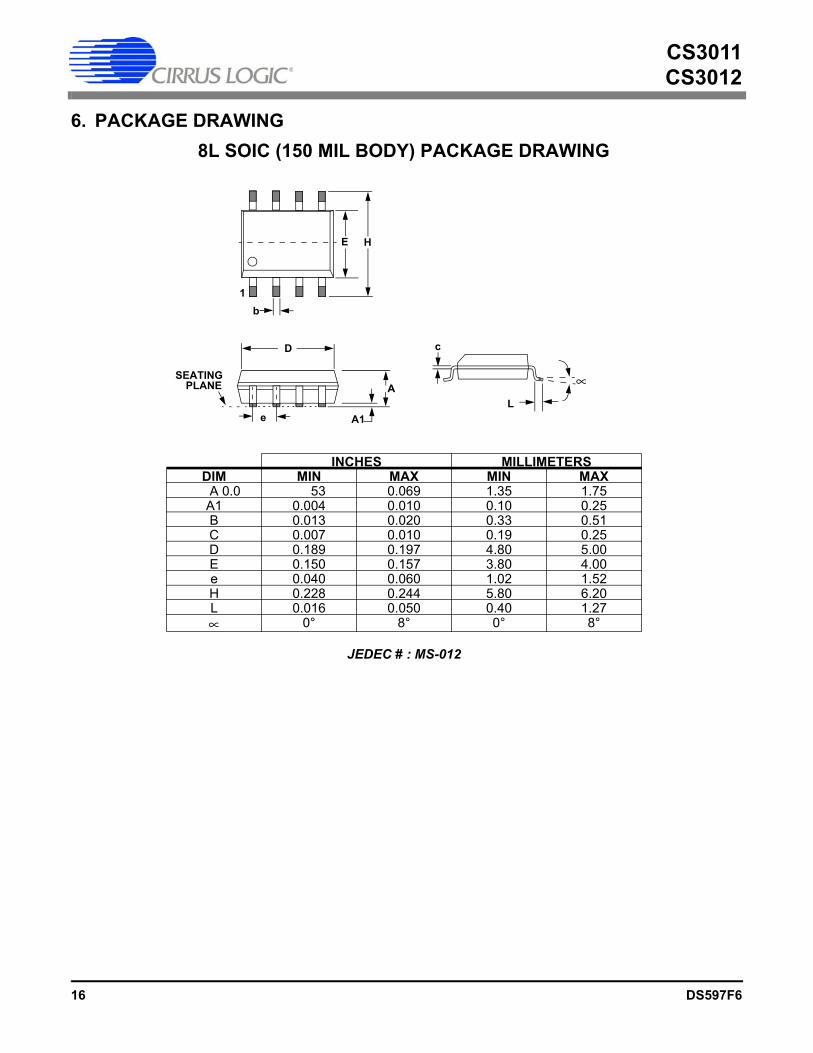
6. PACKAGE DRAWING
INCHES MILLIMETERSDIM MIN MAX MIN MAX
A 0.0 53 0.069 1.35 1.75A1 0.004 0.010 0.10 0.25B 0.013 0.020 0.33 0.51C 0.007 0.010 0.19 0.25D 0.189 0.197 4.80 5.00E 0.150 0.157 3.80 4.00e 0.040 0.060 1.02 1.52H 0.228 0.244 5.80 6.20L 0.016 0.050 0.40 1.27∝ 0° 8° 0° 8°
JEDEC # : MS-012
8L SOIC (150 MIL BODY) PACKAGE DRAWING
D
HE
e
b
A1
A
c
L
∝SEATINGPLANE
1

CS3011CS3012
DS597F6 17
7. REVISION HISTORY Revision Date Changes
F2 SEP 2004 Added lead-free device ordering information.F3 AUG 2005 Added MSL specifications. Updated legal notice. Added leaded (Pb) devices.F4 AUG 2006 Updated Typical Performance Plots. Removed Powerdown feature.F5 NOV 2007 Added additional information regarding open-loop and gain stability compensation.F6 JUL 2009 Removed lead-containing SOICs from ordering information.
CS3011CS3012
18 DS597F6
Contacting Cirrus Logic SupportFor all product questions and inquiries contact a Cirrus Logic Sales Representative. To find the one nearest to you go to www.cirrus.com
IMPORTANT NOTICECirrus Logic, Inc. and its subsidiaries (“Cirrus”) believe that the information contained in this document is accurate and reliable. However, the information is subjectto change without notice and is provided “AS IS” without warranty of any kind (express or implied). Customers are advised to obtain the latest version of relevantinformation to verify, before placing orders, that information being relied on is current and complete. All products are sold subject to the terms and conditions of salesupplied at the time of order acknowledgment, including those pertaining to warranty, indemnification, and limitation of liability. No responsibility is assumed by Cirrusfor the use of this information, including use of this information as the basis for manufacture or sale of any items, or for infringement of patents or other rights of thirdparties. This document is the property of Cirrus and by furnishing this information, Cirrus grants no license, express or implied under any patents, mask work rights,copyrights, trademarks, trade secrets or other intellectual property rights. Cirrus owns the copyrights associated with the information contained herein and gives con-sent for copies to be made of the information only for use within your organization with respect to Cirrus integrated circuits or other products of Cirrus. This consentdoes not extend to other copying such as copying for general distribution, advertising or promotional purposes, or for creating any work for resale.
CERTAIN APPLICATIONS USING SEMICONDUCTOR PRODUCTS MAY INVOLVE POTENTIAL RISKS OF DEATH, PERSONAL INJURY, OR SEVERE PROP-ERTY OR ENVIRONMENTAL DAMAGE (“CRITICAL APPLICATIONS”). CIRRUS PRODUCTS ARE NOT DESIGNED, AUTHORIZED OR WARRANTED FOR USEIN PRODUCTS SURGICALLY IMPLANTED INTO THE BODY, AUTOMOTIVE SAFETY OR SECURITY DEVICES, LIFE SUPPORT PRODUCTS OR OTHER CRIT-ICAL APPLICATIONS. INCLUSION OF CIRRUS PRODUCTS IN SUCH APPLICATIONS IS UNDERSTOOD TO BE FULLY AT THE CUSTOMER'S RISK AND CIR-RUS DISCLAIMS AND MAKES NO WARRANTY, EXPRESS, STATUTORY OR IMPLIED, INCLUDING THE IMPLIED WARRANTIES OF MERCHANTABILITY ANDFITNESS FOR PARTICULAR PURPOSE, WITH REGARD TO ANY CIRR US PRODUCT THAT IS USED IN SUCH A MANNER. IF THE CUSTOMER OR CUS-TOMER'S CUSTOMER USES OR PERMITS THE USE OF CIRRUS PRODUCTS IN CRITICAL APPLICATIONS, CUSTOMER AGREES, BY SUCH USE, TO FULLYINDEMNIFY CIRRUS, ITS OFFICERS, DIRECTORS, EMPLOYEES, DISTRIBUTORS AND OTHER AGENTS FROM ANY AND ALL LIABILITY, INCLUDING AT-TORNEYS' FEES AND COSTS, THAT MAY RESULT FROM OR ARISE IN CONNECTION WITH THESE USES.Cirrus Logic, Cirrus, and the Cirrus Logic logo designs are trademarks of Cirrus Logic, Inc. All other brand and product names in this document may be trademarksor service marks of their respective owners.
Mouser Electronics
Authorized Distributor
Click to View Pricing, Inventory, Delivery & Lifecycle Information: Cirrus Logic:
CS3011-IS CS3011-ISZ CS3011-ISZR CS3012-IS CS3012-ISZ CS3012-ISZR
Related Documents