© 2010 WILEY-VCH Verlag GmbH & Co. KGaA, Weinheim Adv. Mater. 2010, 22, 2919–2938 2919 www.advmat.de www.MaterialsViews.com REVIEW DOI: 10.1002/adma.200904306 Crystalline Oxides on Silicon 1. Introduction Thin film oxides on silicon have enabled the digital revolution. A simple metal-oxide-semiconductor (MOS) structure, con- sisting of metal placed on top of an oxide that is in turn placed on top of silicon, forms the basis of capacitors that function as memory and field-effect transistors (FETs) that compute. While this combination of materials is simple, its impact on our society has been revolutionary. To date, the most technologically important oxide has been an amorphous thin film of SiO 2 . This amorphous SiO 2 layer readily forms a nearly electrically perfect interface on the (001) face of silicon. As a result, devices based on this material system domi- nate electronics: the number of MOS transistors (MOSFETs) produced per year, greater than 10 18 , exceeds the annual number of raindrops falling on the state of California. [1] Due to intensive research efforts, the speed and density of transis- tors has been steadily increasing for decades, doubling roughly every 18 months, a trend known as Moore’s law. [2,3] The tech- nological focus on silicon devices, and the resulting ubiquity of these devices, has established and maintained silicon as the most advanced device materials platform for decades. The ability to integrate crystalline complex oxides on silicon presents opportunities to extend and enhance silicon technology. In the last decade, complex oxides have been explored as a replacement for SiO 2 in MOSFETs in order to overcome funda- mental physical limitations to further per- formance enhancements with SiO 2 -based structures. Continual improvements in transistor performance require MOSFETs to be made physically smaller with each new generation of devices. Continuation of this process using SiO 2 as the dielectric layer has become untenable since the nec- essary SiO 2 layer would be too thin (1 nm) to act as an effective insulator. Thus, new materials for the gate oxide must be found with higher dielectric constants (“high- k oxides”). [4] This device application takes advantage of the large dielectric constants available in complex oxides. In 1998, crys- talline SrTiO 3 was fabricated in a MOS device with perform- ance characteristics corresponding to an equivalent oxide thick- ness (EOT) in an SiO 2 -based MOS structure of less than 1 nm, the first time that such a result had been demonstrated (see Figure 1). [5–7] This accomplishment was made possible by the high dielectric constant of SrTiO 3 and fabrication techniques that allow atomically abrupt interfaces between SrTiO 3 and silicon to be formed and avoid the formation of a low-dielectric- constant interfacial region. Functional complex oxides, such as ferroelectrics, have also been considered as replacements for SiO 2 in MOSFETs. The first application of this sort was proposed in the 1950’s and was directed at fabricating a ferroelectric FET. [8–11] In the usual MOSFET, the electric field across the dielectric oxide (created by the applied voltage between the gate and semiconductor) controls the FET behavior. With a ferroelectric replacing the dielectric oxide, the nonvolatile polarization of the ferroelectric performs the same function as this electric field, enabling the transistor to remain either on or off in the absence of an applied voltage. In early attempts to create this device, researchers glued single-crystal ferroelectric BaTiO 3 onto silicon (see Figure 2). While that approach failed due to the lack of coupling between the BaTiO 3 and silicon, recently developed deposition techniques have brought the realization of this device much closer to reality. While this replacement of an amorphous die- lectric oxide with a crystalline ferroelectric oxide is conceptually simple, it transforms the capabilities of the resulting transistor by enabling nonvolatile operation, dramatically lowering the power requirements of the device. This review addresses the technical challenges involved in realizing such crystalline oxides on silicon devices. We focus on crystalline oxides rather than amorphous or polycrystalline By James W. Reiner, Alexie M. Kolpak, Yaron Segal, Kevin F. Garrity, Sohrab Ismail-Beigi, Charles H. Ahn, and Fred J. Walker* This review outlines developments in the growth of crystalline oxides on the ubiquitous silicon semiconductor platform. The overall goal of this endeavor is the integration of multifunctional complex oxides with advanced semicon- ductor technology. Oxide epitaxy in materials systems achieved through con- ventional deposition techniques is described first, followed by a description of the science and technology of using atomic layer-by-layer deposition with molecular beam epitaxy (MBE) to systematically construct the oxide–silicon interface. An interdisciplinary approach involving MBE, advanced real-space structural characterization, and first-principles theory has led to a detailed understanding of the process by which the interface between crystalline oxides and silicon forms, the resulting structure of the interface, and the link between structure and functionality. Potential applications in electronics and photonics are also discussed. [∗] Dr. J. W. Reiner, Dr. A. M. Kolpak, Y. Segal, K. F. Garrity, Prof. S. Ismail-Beigi, Prof. C. H. Ahn, Dr. F. J. Walker Yale University, P.O. Box 208284 New Haven, CT 06520-8284 (USA) E-mail: [email protected]

Welcome message from author
This document is posted to help you gain knowledge. Please leave a comment to let me know what you think about it! Share it to your friends and learn new things together.
Transcript

www.advmat.dewww.MaterialsViews.com
REV
Crystalline Oxides on SiliconIEW
By James W. Reiner , Alexie M. Kolpak , Yaron Segal , Kevin F. Garrity , Sohrab Ismail-Beigi , Charles H. Ahn , and Fred J. Walker *This review outlines developments in the growth of crystalline oxides on the ubiquitous silicon semiconductor platform. The overall goal of this endeavor is the integration of multifunctional complex oxides with advanced semicon-ductor technology. Oxide epitaxy in materials systems achieved through con-ventional deposition techniques is described fi rst, followed by a description of the science and technology of using atomic layer-by-layer deposition with molecular beam epitaxy (MBE) to systematically construct the oxide–silicon interface. An interdisciplinary approach involving MBE, advanced real-space structural characterization, and fi rst-principles theory has led to a detailed understanding of the process by which the interface between crystalline oxides and silicon forms, the resulting structure of the interface, and the link between structure and functionality. Potential applications in electronics and photonics are also discussed.
1. Introduction
Thin fi lm oxides on silicon have enabled the digital revolution. A simple metal-oxide-semiconductor (MOS) structure, con-sisting of metal placed on top of an oxide that is in turn placed on top of silicon, forms the basis of capacitors that function as memory and fi eld-effect transistors (FETs) that compute. While this combination of materials is simple, its impact on our society has been revolutionary.
To date, the most technologically important oxide has been an amorphous thin fi lm of SiO 2 . This amorphous SiO 2 layer readily forms a nearly electrically perfect interface on the (001) face of silicon. As a result, devices based on this material system domi-nate electronics: the number of MOS transistors (MOSFETs) produced per year, greater than 10 18 , exceeds the annual number of raindrops falling on the state of California. [ 1 ] Due to intensive research efforts, the speed and density of transis-tors has been steadily increasing for decades, doubling roughly every 18 months, a trend known as Moore’s law. [ 2 , 3 ] The tech-nological focus on silicon devices, and the resulting ubiquity of these devices, has established and maintained silicon as the most advanced device materials platform for decades.
The ability to integrate crystalline complex oxides on silicon presents opportunities to extend and enhance silicon technology.
© 2010 WILEY-VCH Verlag GmbH & Co. KGaA, WeinheimAdv. Mater. 2010, 22, 2919–2938
DOI: 10.1002/adma.200904306
[∗] Dr. J. W. Reiner, Dr. A. M. Kolpak, Y. Segal, K. F. Garrity, Prof. S. Ismail-Beigi, Prof. C. H. Ahn, Dr. F. J. Walker Yale University, P.O. Box 208284New Haven, CT 06520-8284 (USA) E-mail: [email protected]
In the last decade, complex oxides have been explored as a replacement for SiO 2 in MOSFETs in order to overcome funda-mental physical limitations to further per-formance enhancements with SiO 2 -based structures. Continual improvements in transistor performance require MOSFETs to be made physically smaller with each new generation of devices. Continuation of this process using SiO 2 as the dielectric layer has become untenable since the nec-essary SiO 2 layer would be too thin (1 nm) to act as an effective insulator. Thus, new materials for the gate oxide must be found with higher dielectric constants (“high- k oxides”). [ 4 ] This device application takes advantage of the large dielectric constants available in complex oxides. In 1998, crys-
talline SrTiO 3 was fabricated in a MOS device with perform-ance characteristics corresponding to an equivalent oxide thick-ness (EOT) in an SiO 2 -based MOS structure of less than 1 nm, the fi rst time that such a result had been demonstrated (see Figure 1 ). [ 5–7 ] This accomplishment was made possible by the high dielectric constant of SrTiO 3 and fabrication techniques that allow atomically abrupt interfaces between SrTiO 3 and silicon to be formed and avoid the formation of a low-dielectric-constant interfacial region.
Functional complex oxides, such as ferroelectrics, have also been considered as replacements for SiO 2 in MOSFETs. The fi rst application of this sort was proposed in the 1950’s and was directed at fabricating a ferroelectric FET. [ 8–11 ] In the usual MOSFET, the electric fi eld across the dielectric oxide (created by the applied voltage between the gate and semiconductor) controls the FET behavior. With a ferroelectric replacing the dielectric oxide, the nonvolatile polarization of the ferroelectric performs the same function as this electric fi eld, enabling the transistor to remain either on or off in the absence of an applied voltage. In early attempts to create this device, researchers glued single-crystal ferroelectric BaTiO 3 onto silicon (see Figure 2 ). While that approach failed due to the lack of coupling between the BaTiO 3 and silicon, recently developed deposition techniques have brought the realization of this device much closer to reality. While this replacement of an amorphous die-lectric oxide with a crystalline ferroelectric oxide is conceptually simple, it transforms the capabilities of the resulting transistor by enabling nonvolatile operation, dramatically lowering the power requirements of the device.
This review addresses the technical challenges involved in realizing such crystalline oxides on silicon devices. We focus on crystalline oxides rather than amorphous or polycrystalline
2919
2920
REV
IEW
www.advmat.dewww.MaterialsViews.com
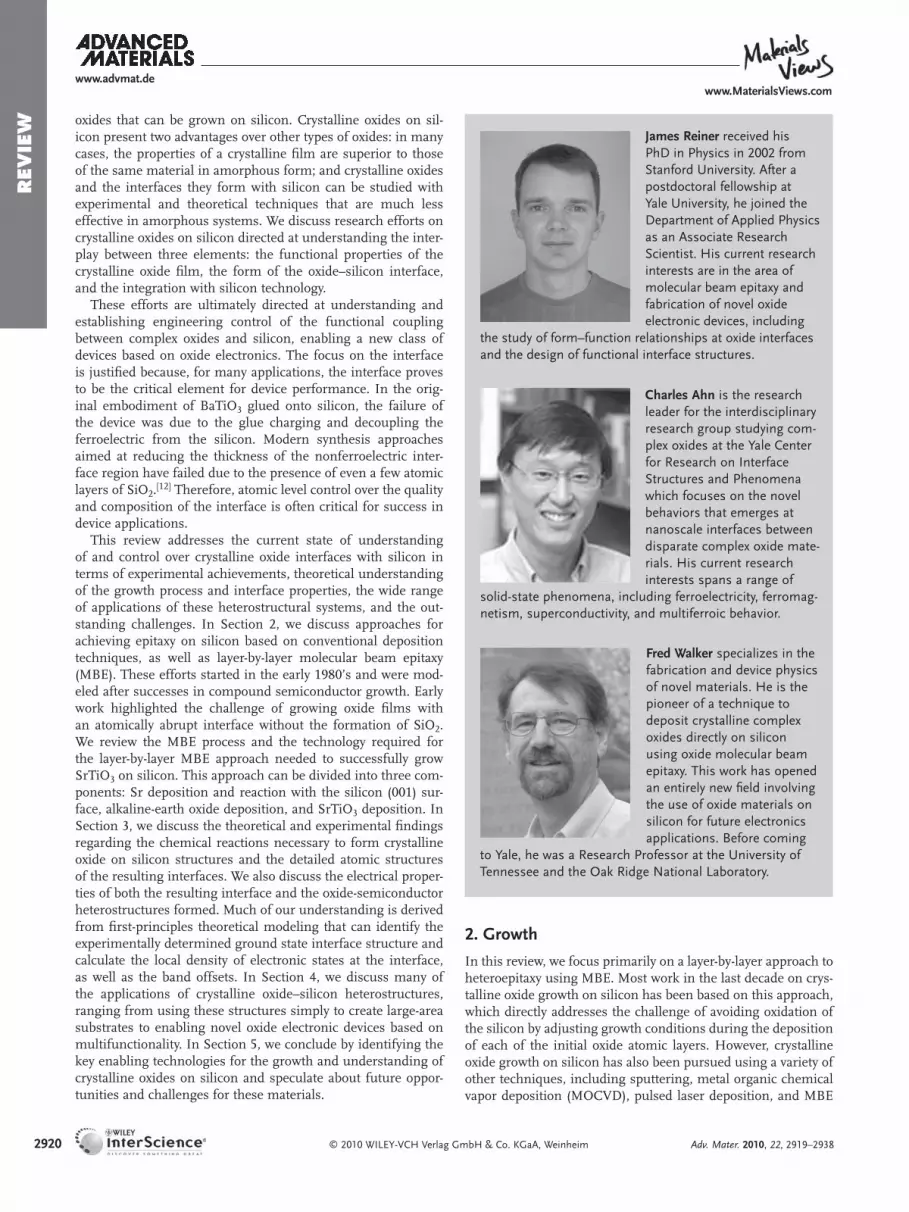
James Reiner received his PhD in Physics in 2002 from Stanford University. After a postdoctoral fellowship at Yale University, he joined the Department of Applied Physics as an Associate Research Scientist. His current research interests are in the area of molecular beam epitaxy and fabrication of novel oxide electronic devices, including
the study of form–function relationships at oxide interfaces and the design of functional interface structures.
Charles Ahn is the research leader for the interdisciplinary research group studying com-plex oxides at the Yale Center for Research on Interface Structures and Phenomena which focuses on the novel behaviors that emerges at nanoscale interfaces between disparate complex oxide mate-rials. His current research interests spans a range of
solid-state phenomena, including ferroelectricity, ferromag-netism, superconductivity, and multiferroic behavior.
Fred Walker specializes in the fabrication and device physics of novel materials. He is the pioneer of a technique to deposit crystalline complex oxides directly on silicon using oxide molecular beam epitaxy. This work has opened an entirely new fi eld involving the use of oxide materials on silicon for future electronics applications. Before coming
to Yale, he was a Research Professor at the University of Tennessee and the Oak Ridge National Laboratory.
oxides that can be grown on silicon. Crystalline oxides on sil-icon present two advantages over other types of oxides: in many cases, the properties of a crystalline fi lm are superior to those of the same material in amorphous form; and crystalline oxides and the interfaces they form with silicon can be studied with experimental and theoretical techniques that are much less effective in amorphous systems. We discuss research efforts on crystalline oxides on silicon directed at understanding the inter-play between three elements: the functional properties of the crystalline oxide fi lm, the form of the oxide–silicon interface, and the integration with silicon technology.
These efforts are ultimately directed at understanding and establishing engineering control of the functional coupling between complex oxides and silicon, enabling a new class of devices based on oxide electronics. The focus on the interface is justifi ed because, for many applications, the interface proves to be the critical element for device performance. In the orig-inal embodiment of BaTiO 3 glued onto silicon, the failure of the device was due to the glue charging and decoupling the ferroelectric from the silicon. Modern synthesis approaches aimed at reducing the thickness of the nonferroelectric inter-face region have failed due to the presence of even a few atomic layers of SiO 2 . [ 12 ] Therefore, atomic level control over the quality and composition of the interface is often critical for success in device applications.
This review addresses the current state of understanding of and control over crystalline oxide interfaces with silicon in terms of experimental achievements, theoretical understanding of the growth process and interface properties, the wide range of applications of these heterostructural systems, and the out-standing challenges. In Section 2, we discuss approaches for achieving epitaxy on silicon based on conventional deposition techniques, as well as layer-by-layer molecular beam epitaxy (MBE). These efforts started in the early 1980’s and were mod-eled after successes in compound semiconductor growth. Early work highlighted the challenge of growing oxide fi lms with an atomically abrupt interface without the formation of SiO 2 . We review the MBE process and the technology required for the layer-by-layer MBE approach needed to successfully grow SrTiO 3 on silicon. This approach can be divided into three com-ponents: Sr deposition and reaction with the silicon (001) sur-face, alkaline-earth oxide deposition, and SrTiO 3 deposition. In Section 3, we discuss the theoretical and experimental fi ndings regarding the chemical reactions necessary to form crystalline oxide on silicon structures and the detailed atomic structures of the resulting interfaces. We also discuss the electrical proper-ties of both the resulting interface and the oxide-semiconductor heterostructures formed. Much of our understanding is derived from fi rst-principles theoretical modeling that can identify the experimentally determined ground state interface structure and calculate the local density of electronic states at the interface, as well as the band offsets. In Section 4, we discuss many of the applications of crystalline oxide–silicon heterostructures, ranging from using these structures simply to create large-area substrates to enabling novel oxide electronic devices based on multifunctionality. In Section 5, we conclude by identifying the key enabling technologies for the growth and understanding of crystalline oxides on silicon and speculate about future oppor-tunities and challenges for these materials.
© 2010 WILEY-VCH Verlag G
2. Growth
In this review, we focus primarily on a layer-by-layer approach to heteroepitaxy using MBE. Most work in the last decade on crys-talline oxide growth on silicon has been based on this approach, which directly addresses the challenge of avoiding oxidation of the silicon by adjusting growth conditions during the deposition of each of the initial oxide atomic layers. However, crystalline oxide growth on silicon has also been pursued using a variety of other techniques, including sputtering, metal organic chemical vapor deposition (MOCVD), pulsed laser deposition, and MBE
mbH & Co. KGaA, Weinheim Adv. Mater. 2010, 22, 2919–2938

REV
IEW
www.advmat.dewww.MaterialsViews.com
Figure 1. The challenge for integrating crystalline oxides with silicon is achieving an atomically abrupt interface (a, inset). The capacitance per area of the resulting structure can be very large, as shown in panel b. Here the capacitance of the oxide is measured at large negative applied voltages. Panel a is reproduced with permission from Ref. [ 119 ] . Copyright 2009, American Association for the Advancement of Science. Panel b is reproduced with permission from Ref. [ 5 ] . Copyright 2009, American Physical Society.
co-evaporation, where the fi lm growth is essentially continuousrather than layer-by-layer. [ 13 ] We discuss fi rst results from theseother techniques, which highlight both the opportunities andchallenges inherent in realizing crystalline oxide on silicon sys-tems. This discussion is followed by a description of advancedMBE techniques, after which we discuss the layer-by-layer depo-sition approach made possible by these techniques. Throughout
© 2010 WILEY-VCH Verlag GAdv. Mater. 2010, 22, 2919–2938
Figure 2. One novel application for crystalline oxides on silicon involves nonvolatile computing using a ferroelectric FET. While a patent for this device was fi led over 50 years ago (a), [ 11 ] only recently have the neces-sary fabrication techniques been discovered. In a ferroelectric transistor, the gate oxide is replaced by a ferroelectric, which has a permanent up or down polarization (b). The ferroelectric turns the transistor on or off (allowing or blocking current fl owing between the source ( V s ) and drain ( V d ) potentials) without the need of a continuous gate voltage, V g , making the device nonvolatile.
most of this review, we focus on the silicon (001) surface, since this surface is by far the most technologically important surface of silicon. However, we also briefl y discuss interesting recent results on crystalline oxide growth on the silicon (111) surface.
2.1. Continuous Deposition
Conceptually, the most promising candidate materials for epi-taxial growth on silicon would be crystalline oxides that match silicon in both structure and chemistry. If an epitaxial struc-ture is to form, the lattice parameters must match closely, the symmetry of the crystal faces for silicon and the oxide must be compatible, and undesirable compounds must not form due to interdiffusion. Once a suitable oxide is found, the remainder of the procedure may seem conceptually simple—join two bulk crystals together—but in practice this approach is not possible (Figure 1 ). Instead, a common approach used in both research and industry to form (i.e., grow) a crystalline fi lm on a substrate is to condense the fi lm from the vapor phase.
One important factor affecting oxide growth on silicon that was recognized early [ 14 ] is the potential for a chemical reaction of the oxide with silicon. For example, for the oxide ZrO 2 , the key reac-tions that may take place at the interface are: ZrO 2 + 2Si → ZrSi + SiO 2 and ZrO 2 + Si → Zr + SiO 2 . If all of the reactions from ZrO 2 and silicon to stable compounds of Zr, silicon, and oxygen are endothermic, then the oxide is stable with respect to reaction with silicon. A comprehensive study of all of the binary oxides in the periodic table was published by Hubbard and Schlom in 1996. [ 15 ] This work found that a small subset of oxides, primarily the alkaline-earth binary oxides, are stable with respect to reac-tion with silicon up to a temperature of 1000 K. The question of how the details of an oxide–semiconductor interface might modify the bulk thermodynamics has also been considered. [ 16 ]
2921mbH & Co. KGaA, Weinheim

2922
REV
IEW
www.advmat.dewww.MaterialsViews.com
2.1.1. Mg 2 Al 2 O 4
One of the fi rst crystalline oxides to be grown epitaxially on sil-icon was the spinel material, MgAl 2 O 4 (MGA). [ 17 ] The original work was directed at depositing a crystalline oxide on silicon as a route to achieving silicon-on-insulator (SOI) structures. Epitaxy of the MGA spinel was accomplished using MOCVD, followed by MOCVD growth of silicon to achieve the SOI structure. After the discovery of high-temperature ( T c ) super-conductivity, MGA growth on silicon was also used to create a buffer layer for the growth of the high- T c superconductors on silicon. [ 18 ] This MOCVD approach leads to the formation of an amorphous layer at the MGA–Si interface. However, epitaxy is still possible since this layer forms after the crystalline orienta-tion of the MGA has been established. [ 19 ] In these applications, which involve the MGA acting as a buffer layer for subsequent epitaxial growth, the quality of the surface layer of the MGA is of paramount importance, instead of the properties of the MGA–Si interface itself. However, for applications requiring an electrical coupling between the oxide and silicon, an amor-phous interface of this sort is generally undesirable.
In addition to questions about deposition technique and chemical stability at the interface, an additional set of considera-tions in crystalline oxide epitaxy on silicon concerns the com-patibility of the crystal lattices between the oxide material and silicon. These lattice matching issues determine many of the details of the resulting epitaxy. In the case of MGA, the size of the lattice constant relative to silicon introduces a partial incom-patibility, which prevents single-crystal MGA fi lm growth on sil-icon. Under appropriate growth conditions, MGA grows on sil-icon such that the a -axis of the cubic MGA lattice lines up with the a -axis of the unit cell of the silicon (001) surface; three a -axis lattice spacings of silicon match two a -axis lattice spacings of MGA to within 1%. [ 19 ] Such a small lattice mismatch is normally favorable for single-crystal epitaxy. However, MGA growth on silicon leads to formation of a polycrystalline fi lm. The reason is that, because the MGA fi lm nucleates as isolated islands at various unrelated locations on the silicon surface, the alignment between the MGA and silicon will not be consistent due to the 2:3 ratio of the MGA and silicon lattice constants. Therefore, the lattice of the MGA fi lm will be discontinuous where the islands grow together, leading to numerous grain boundaries, resulting in a heavily faulted fi lm and a rough surface. [ 19 ]
2.1.2. MgO
Another crystalline oxide material that was a focus of early study is MgO. It has been deposited using a variety of techniques, including laser ablation [ 20 ] and MBE. [ 21 ] Unlike the case of MGA discussed above, the lattice mismatch between MgO and silicon is large, about 10%. This mismatch leads to a high density of misfi t dislocations at the MgO–Si interface that suppress the crystalline quality of the MgO fi lm until a relatively thick (10 nm) fi lm has been deposited. Moreover, like MGA, the MgO fi lm does not nucleate on the silicon surface in a manner that will lead to a single-crystalline fi lm; the ratio of lattice constants in MgO and silicon is 3:4. As a result, MgO fi lms grown on silicon are polycrystalline. However, unlike MGA, the inter-face between MgO and silicon is atomically abrupt for pulsed
© 2010 WILEY-VCH Verlag G
laser deposition (PLD)-grown fi lms, while for MBE-grown fi lms about 1 monolayer (ML) of SiO 2 is formed at the interface.
2.1.3. Y 2 O 3 :ZrO 2
An oxide material that can be grown on silicon in single-crystalline, as opposed to polycrystalline, form is Y 2 O 3 :ZrO 2 . [ 14 , 22 , 23 ] For this system, the lattice matching to silicon in an epitaxial structure is cube-on-cube with a mismatch of 5.6%. This cube-on-cube alignment implies that it is possible to grow Y 2 O 3 :ZrO 2 as a single-crystalline fi lm on silicon, since individual islands of Y 2 O 3 :ZrO 2 growing on the silicon surface can merge without grain boundaries. The reactivity of this oxide with silicon is also limited. As a result, relatively abrupt interfaces can be realized experimentally. [ 24 , 25 ] However, the relatively large lattice mis-match substantially degrades the interface region through the formation of misfi t dislocations, even for very thin Y 2 O 3 :ZrO 2 fi lms. Though alloying with a smaller cation is often a tech-nique employed to achieve a superior lattice match, in the case of Y 2 O 3 :ZrO 2 no smaller compatible cation is available.
First-principles calculations of ZrO 2 and the technologi-cally important HfO 2 on silicon (001) reveal a complicated interface. [ 26 ] The complications are due to the polar nature of the fl uorite (001) face of the oxide and the complex chemistry of ZrO 2 and silicon. For the interfaces examined theoretically, predictions span the range from metallic to insulating, with some interfaces having interfacial states located in the silicon bandgap. As we describe below, understanding the details of the experimentally realized interface structure is crucial to pro-viding relevant and accurate theoretical predictions.
2.1.4. Al 2 O 3
A surprising example of the growth of a simple oxide on silicon is that of Al 2 O 3 on silicon (001). This interface system is well known to be chemically stable based on early work concerning silicon deposited on sapphire for SOI applications. [ 27 ] The bulk form of Al 2 O 3 has the hexagonal corundum structure and is therefore incompatible with single-crystal growth on the cubic (001) surface of silicon. Remarkably, a process was discovered for depositing thin fi lms of the γ-phase of Al 2 O 3 on silicon without silicate- or SiO 2 -formation at the interface. The process involves a high temperature, 850 °C, and low oxygen pressures below 10 −8 Torr. [ 28 ] The fi rst two monolayers of the γ-Al 2 O 3 are (001)-oriented and strained to the silicon (001) surface. For thicker fi lms, a transition from (001) orientation to (111) orientation of the Al 2 O 3 occurs, which fully relaxes the Al 2 O 3 . First-principles cal-culations of γ-Al 2 O 3 on silicon (001) fi nd a large bandgap system with no interfacial electronic levels in the bulk bandgaps. [ 29 ]
2.1.5. (La x Y 1−x ) 2 O 3 on Silicon (111)
A range of compositions of (La x Y 1− x ) 2 O 3 can be grown on silicon (111). [ 30 ] For La fractions near 20%, a lattice-matched structure is realized at room temperature. Growth of the oxide on silicon was initiated using two different procedures, with two different results. When the silicon surface is exposed fi rst to the metal fl ux, silicides form at the interface and a rough oxide fi lm results. However, when the silicon surface is exposed to oxygen fi rst,
mbH & Co. KGaA, Weinheim Adv. Mater. 2010, 22, 2919–2938

REV
IEW
www.advmat.dewww.MaterialsViews.com
Figure 3. Schematic of an MBE system. For the growth of a complex oxide, such as BaTiO 3 , elemental Ba and Ti beams are directed at the sub-strate in the presence of a low pressure of oxygen, typically 10 −7 Torr. The metals are heated in effusion cells using resistive heating elements sur-rounding crucibles that contain the metals. When the evaporated metal atoms hit the cold substrate surface, they stick, react with the silicon, and build up the crystal with atomic-layer precision. Refl ection high-energy electron diffraction (RHEED) monitors the crystallography of the growing surface, also with atomic-layer precision.
smooth epitaxial fi lms are created. X-ray diffraction indicates a high degree of crystalline uniformity in the (La x Y 1− x ) 2 O 3 fi lms. Silicon can also be deposited subsequently on the (La x Y 1− x ) 2 O 3 surface for possible silicon-on-insulator applications, forming a smooth (111) oriented fi lm exhibiting a 7 × 7 surface recon-struction. However, the silicon overlayer has a high density of stacking faults and microtwins.
2.1.6. Sc 2 O 3 on Silicon (111)
Many binary insulators with a cubic fl uorite or related crystal structures have been grown epitaxially on silicon (111). One example is Sc 2 O 3 , which has been grown by MBE evaporation of Sc in an oxygen background pressure of 5 × 10 −8 Torr on a clean (111) silicon surface. [ 31 ] Sc 2 O 3 , which processes cubic bixbyite structure, has a 10% lattice mismatch with silicon (111). The resulting strain is relieved by a hexagonal misfi t dislocation net-work. A high density of planar defects is also observed, which have been identifi ed as antiphase boundaries. Their presence is related to the fact that there is not a unique arrangement of the bixbyite structure of the Sc 2 O 3 relative to the silicon surface during initial fi lm nucleation.
2.2. Advanced MBE Deposition
The use of MBE for oxide growth allows researchers to access the richness of properties found in complex oxides, with the atomic-layer precision that is the hallmark of the MBE process. Applying MBE to oxide growth brought with it a new set of chal-lenges not encountered in the more mature fi eld of III–V semi-conductors. These challenges go hand in hand with the variety of composition and structure of the fi lms that can be grown. We review developments in sources for new elements, in situ control of stoichiometry and structure, and integration of physical prop-erties characterization with an MBE chamber. Each of these com-ponents is shown in Figure 3 . These advanced MBE techniques enable the layer-by-layer deposition approach, but are also appli-cable to the continuous deposition techniques discussed above.
2.2.1. Stoichiometry Control
Control over fi lm stoichiometry is a major challenge in oxide fi lm growth. Many oxide compounds form a particular structure (i.e., perovskite) over a wide range of compositions. This fl exi-bility would appear to make composition control less important in crystalline oxide growth. However, in practice the opposite is true, since fi lms grown over this range of compositions will have dramatically different properties, even if the same basic crystal structure forms. The comparison of oxide to III–IV growth is illustrative. Most III–V semiconductor crystals form in a very narrow phase window and, as a result, have a specifi c composi-tion. Therefore, structural probes provide precise information about the stoichiometry of III–V fi lms, both in situ and ex situ. Furthermore, during III–V growth, nonstoichiometric phases are strongly suppressed relative to the stoichiometric com-pounds. In comparison, since crystalline oxides often easily accommodate nonstoichiometric phases, these phases must be suppressed by precise elemental fl ux control during deposition.
© 2010 WILEY-VCH Verlag GmAdv. Mater. 2010, 22, 2919–2938
Additionally, many interesting oxide compounds, such as La x Sr 1− x MnO 3 (LSMO) and PbZr x Ti 1− x O 3 (PZT), are alloys requiring control of three independent metal fl uxes. Finally, many transition metals have multiple oxidation states, so that only within a particular window of growth parameters will the desired phase be fabricated.
As a result of these considerations, accurate fl ux measurement is a cornerstone of precise MBE growth. Quartz crystal micro-balance (QCM) sensors are commonly used to measure the fl ux of each elemental evaporation source by observing the rate of mass accumulation at the substrate position. However, a QCM occludes the fl ux reaching the substrate and thus cannot be used to monitor fl ux stability during growth. The QCM signal is also not element-specifi c, so to verify fl ux ratios, successive measure-ments are required. This can become particularly inconvenient when low fl uxes are involved due to low vapor pressures.
Atomic absorption (AA) fl ux monitoring has been devel-oped for use with many elements. [ 32–34 ] In this technique, two opposing quartz view ports on the MBE chamber are used. Ultraviolet or visible light is emitted from a hollow cathode lamp, enters the chamber and crosses the path of the molec-ular beam where absorption occurs, exits the chamber, and is analyzed using lock-in detection. Techniques that replace the hollow cathode lamp in the AA system with a diode laser have also been demonstrated. [ 35 ] The absorption signal is converted to a fl ux through calibration obtained with another method, such as refl ection high-energy electron diffraction (RHEED) oscillations, X-ray refl ectivity, or Rutherford back scattering. Using AA fl ux measurements, fl ux control of 0.1% during fi lm deposition has been demonstrated. [ 34 ] Since AA monitoring does not interfere with the molecular beam, it can be used as a feedback signal to correct fl ux deviations during fi lm growth. This control during growth is particularly important for oxides because the fl ux of atoms from MBE deposition sources, which
2923bH & Co. KGaA, Weinheim

2924
REV
IEW
www.advmat.dewww.MaterialsViews.com
ideally would depend only the source power or temperature, in practice also depends on background oxygen pressure. [ 36 ]
Precise in situ control of the metal cation stoichiometry in a complex oxide fi lm is possible in the special case of SrTiO 3 using real-time RHEED analysis. [ 37 ] Stoichiometry control is estab-lished by observing the shape of RHEED intensity oscillations during the growth process. Stoichiometric growth expresses itself as intensity oscillations that maintain their amplitude and shape throughout the growth process; excess Sr gives rise to a double-peaked shape of the oscillations, while excess Ti results in a beat frequency appearing in the oscillations. Recently, this method was used to study the effect of nonstoichiometric com-position on SrTiO 3 grown by homoepitaxy on TiO 2 -terminated SrTiO 3 substrates. [ 38 ] Both Sr- and Ti-defi cient fi lms show an expanded out-of-plane lattice constant. Transmission electron microscopy (TEM) analysis shows distinct defect structures for the two cases. Excess Sr resulted in columnar defects attributed to Ruddlesden–Popper phases, while excess Ti resulted in the formation of amorphous regions of TiO 2 .
2.2.2. Oxidation Sources
The goal of oxidation sources is to make available a suffi cient density of oxygen atoms at the substrate such that the desired material is grown. [ 39 ] For example, when O 2 is used to grow iron oxides on sapphire, Fe 2 O 3 fi lms can form when the rate of O 2 arrival and dissociation at the substrate is faster than the rate of Fe atoms arrival and oxidation. At progressively lower oxygen rates, Fe 3 O 4 , FeO, and partially oxidized Fe clusters will form. By periodically adjusting the oxygen growth pressure, multilayer structures having a periodic oxygen content can be grown, e.g., Ti 2 O 3 /TiO. [ 40 ] At the same time, the oxygen pres-sure in the chamber must be low enough to maintain the long mean-free-paths of the molecular beams, to allow RHEED to be used, and to prevent oxidation damage to components inside the chamber.
Some metals, such as Mg, Al, and Ni, oxidize readily even at very low pressures of molecular oxygen. However, for other metals the reactivity of molecular oxygen is not suffi cient for the desired oxides to form. Reactive oxygen sources are used in these cases. Oxygen plasmas may be employed, created either by electron cyclotron resonance (ECR) [ 41 ] or radio-frequency (RF) excitation. [ 42 ] Both techniques create a mix of atomic, molecular, and ionized oxygen, depending on plasma parameters. Thus, the reactivity of the oxygen fl ux and growth outcome depends strongly on these parameters. [ 43 ] The use of an oxygen plasma can also have indirect effects on the grown fi lm. Roughening of TiO 2 fi lms when using an oxygen plasma instead of molecular oxygen has been observed. [ 44 ] This roughening is attributed to a change from a layer-by-layer growth mode to step-fl ow growth under the plasma because of increased mobility of Ti atoms due to the infl uence of the plasma.
Alternatives to oxygen plasma sources are ozone [ 45 ] and NO 2 , which both dissociate easily on substrate surfaces. For ZnO growth, it has been shown that NO 2 enables growth at a pressure three orders of magnitude lower than with molecular oxygen. [ 46 ] Growth rate and photoluminescence yield depend strongly on the Zn/NO 2 fl ux ratio. Oxygen fl ux and activity can be meas-ured by the mass accumulation rate measured by a QCM with
© 2010 WILEY-VCH Verlag G
a silver crystal sensor. [ 42 ] To establish the fl ux and activity of oxygen required to form the desired oxidation state of a partic-ular compound, the change in the mass accumulation rate as a function of oxygen pressure during complex oxide fi lm growth can be monitored. [ 47 ] The mass accumulation rate increases with oxygen pressure, corresponding to oxidation of the metal atoms adsorbed onto the QCM. The rate saturates at a value derived from the oxide mass, when complete oxidation is achieved.
2.2.3. High-Flux Sources
Transition metals are often at the chemically, electronically, or magnetically active sites in complex oxides crystal lattices. How-ever, the low vapor pressures of some transition metals, such as Ti, V, Nb, and Y, require evaporation sources that use very high temperatures, typically above 1600 °C. Even at these elevated tem-peratures, evaporation rates are low, usually less than 10 Å min −1 . Recently, there have been research efforts to integrated concepts from chemical vapor deposition with oxide MBE to enhance the growth rate of transition metal oxides, such as LiNbO 3 , SrTiO 3 , and TiO 2 .
The case of LiNbO 3 , a hexagonal ferroelectric oxide with a very high Curie temperature (1140 °C), is attractive because of the possibility of integrating it with hexagonal wide-bandgap semiconductors such as GaN and SiC. However, Nb evapora-tion by conventional MBE sources is limited to low fl uxes due to the low vapor pressure of Nb even above 2000 °C. To overcome the challenge, LiNbO 3 has been grown using NbCl 5 evaporated at low temperature from an effusion cell instead of a more conventional electron-beam Nb source. [ 48 ] The growth of the LiNbO 3 proceeds by co-evaporating Li metal and NbCl 5 and exposing the substrate to oxygen, promoting the reaction 2Li + 2NbCl 5 + 3O 2 → 2LiNbO 3 + 5Cl 2 . Secondary ion mass spectroscopy (SIMS) shows no Cl incorporated into the LiNbO 3 fi lm, and the chamber pressure during growth is low enough for RHEED to be used.
A different approach based on chemical vapor deposition has been employed to grow TiO 2 [ 44 ] and SrTiO 3 [ 44 ] fi lms. Ti(OC 3 H 7 ) 4 (TTIP) is evaporated at low temperature, giving a beam equiva-lent Ti pressure in the mid 10 −6 Torr range. The Ti precursor allows growth of stoichiometric oxides with rates of up to 125 nm h −1 . In addition, the presence of oxygen in the prec-usor gas facilitates TiO 2 growth without an oxygen source and prevents the formation of oxygen vacancies in SrTiO 3 , thereby producing insulating fi lms. At elevated substrate temperatures, TTIP desorption increases, while the Sr sticking coeffi cient remains close to unity, which has been shown to widen the range of TTIP:Sr ratios for which stoichiometric SrTiO 3 fi lms can be produced.
2.2.4. In situ Analysis Techniques
There is particular interest in the ability to perform in situ spectroscopic, scanning probe, and transport measurement on MBE-grown oxide heterostructures. A compelling reason for such an approach is that oxides exhibit intricate surface struc-tures, and in the case of conducting samples, the surface can be investigated using in situ scanning tunneling microscopy (STM). Another need for in situ analysis concerns the stability
mbH & Co. KGaA, Weinheim Adv. Mater. 2010, 22, 2919–2938

REV
IEW
www.advmat.dewww.MaterialsViews.com
of the oxide fi lms. Some oxides such as MgO readily form hydroxides in air, while others such as EuO are unstable against additional oxidation in air, making it diffi cult or impossible to transfer these samples in air.
The study under ultrahigh-vacuum (UHV) conditions of the near-surface band structure, band offsets, and interfacial states has been done for semiconductors for several decades, providing crucial information about these materials. In order to apply these techniques to oxide systems, a small number of groups have built multichamber systems containing an oxide MBE chamber, augmented with instruments such as X-ray and ultraviolet photoelectron spectrometers, scanning tun-neling microscopes, metallization chambers, and UHV probe stations. [ 49 ] These in situ tools allow for extensive characteri-zation, including capacitance–voltage, sheet resistivity, charge density, and experimental band structure determination. [ 50 , 51 ]
2.3. Layer-by-Layer MBE Growth
The layer-by-layer MBE approach to the epitaxial growth of oxides on silicon has a number of advantages over continuous deposition techniques. The most signifi cant of these is the ability to adjust the growth conditions for the fi lm to meet the thermodynamic stability requirements of each depos-ited atomic layer. In this way, stable epitaxial structures can be designed and built one layer at a time in situations where continuous deposition would lead to undesirable and uncon-trollable chemical reactions at the interface. This MBE growth technique requires both an understanding of the thermody-namics relevant for the materials and the ability, described above, to deliver each of the elements in the structure at a controlled rate to an atomically clean substrate in a controlled background pressure of oxygen.
Epitaxial growth of complex oxides on silicon is far from straightforward. Much of the diffi culty stems from the fact that a crystalline oxide on a semiconductor heterostructure must transition from a network of strongly covalent bonds in the silicon to a mode of primarily ionic bonding in the oxide over a length-scale of less than a nanometer. [ 52 ] This situation is clearly different from the more familiar and well-developed case of compound semiconductor heteroepitaxial systems, where the nature of the covalent bonding and the crystal lattice is unchanged across the interface. For this reason, controlling the heteroepitaxial transition requires careful attention to the thermodynamics of each layer during growth, in addition to the overall fi lm stoichiometry. The oxygen activity and silicon tem-perature must be manipulated to avoid the formation of an amorphous SiO 2 layer that would inhibit epitaxy.
It is not clear a priori what type of interface structure will facilitate this transition, but it is reasonable to assume that, like the well-known Si–SiO 2 interface, the minimum energy inter-face will be amorphous for most stoichiometries. This situation makes it diffi cult to determine the most effective initial oxide deposition sequence without prior knowledge of the interface structure. In addition, it is diffi cult to predict the interface structure without previous experimental data to impose con-straints on the large phase space of possible structures and compositions.
© 2010 WILEY-VCH Verlag GmAdv. Mater. 2010, 22, 2919–2938
A layer-by-layer MBE process was fi rst applied to resolving this growth challenge on silicon for alkaline earth oxides and for the perovskite oxide SrTiO 3 . SrTiO 3 is the most studied complex oxide on silicon (001) and can be fabricated with the highest degree of crystallinity. A handful of other oxides with similar crystal structures have also been successfully grown on silicon (001), such as SrHfO 3 [ 50 ] and BaTiO 3 , [ 53 ] but with less crystallinity. Attempts have been made to grow thin fi lms of other complex oxides with lower expected reactivities [ 15 ] and larger bandgaps, such as LaAlO 3 , [ 54–58 ] but no direct path has been found to date. Understanding the details of how SrTiO 3 grows on silicon is thus an important fi rst step in both discov-ering new paths for growing new oxides on silicon and in con-trolling device functionality at the atomic scale.
2.3.1. Sr Submonolayer Coverage on Silicon (001)
Sr and other alkaline earth metals can be deposited on silicon to form homogeneous surface phases that are one atomic layer thick [ 5 , 53 , 59 , 60 ] without the interface reaction problems posed by oxygen, Ti, or other elements. These results have motivated dep-osition procedures that ensure a Sr-rich condition at the inter-face with silicon in order to avoid reactions between Ti, oxygen, and silicon that lead to structures that are incompatible with perovskite epitaxy. This Sr-rich condition has been established in most growth procedures by depositing a submonolayer of Sr directly on the clean silicon (001) surface as a fi rst step in crys-talline oxide epitaxy. Alternatively, the Sr can be deposited on the silicon before the native oxide has been desorbed. [ 61 ] The presence of Sr catalyzes the thermal desorption of the SiO 2 , leading to a lower temperature to remove this layer. Some of the Sr remains on the silicon surface after the SiO 2 is com-pletely desorbed, creating surface structures that are similar to direct deposition of Sr on a clean silicon (001) surface.
There are two roles played by the Sr submonolayer in pro-moting epitaxy. The fi rst is that it can provide an atomic-level structural template that is compatible with the growth of the oxide. Experiments have examined the role played by a 1/2 monol-ayer (ML) of Sr on silicon (001), a surface layer that is known to stabilize the silicon surface and promote epitaxy. It has been suggested that it is the formation of a complex silicate at the interface that contributes to epitaxy. [ 62 ] Structural determina-tions, however, show that this interface is not a silicate in the traditional sense, but instead is derived from the starting 2 × 1 surface phase of Sr:Si(001). [ 63 ] This physical picture of the role of the surface phase in creating the interface will be discussed in more detail in Section 3.1.
The second role of the alkali earth surface phase is to pre-vent oxidation of the silicon when it is exposed to molecular oxygen, which would create an amorphous layer. [ 62 , 64 ] This pas-sivation role of the Sr depends strongly on the composition of the surface. At a 1/2 ML of Sr, the silicon (001) surface dangling bonds are passivated, and the reactivity of the surface to oxygen is reduced. [ 65 ] This reduced reactivity with oxygen is critical in promoting the epitaxy of alkaline earth oxides and SrTiO 3 on sil-icon. Although the atomic structure of the 1/2 ML Sr on silicon is relatively simple, the actual surface chemical reactions that lead up to this structure during oxide epitaxy are found to be com-plicated; these reactions are discussed in Section 3.1.
2925bH & Co. KGaA, Weinheim

2926
REV
IEW
www.advmat.dewww.MaterialsViews.com
Figure 4. Plan view TEM image of SrTiO 3 grown on silicon. For very thin fi lms, island formation is observed. The bright areas correspond to thicker islands, which have a high degree of coherency, as shown by resolving the atomic columns. Eliminating this island formation is an ongoing research challenge. Reproduced with permission from Ref. [ 98 ] . Copyright 2008, American Physical Society.
2.3.2. Alkaline Earth Oxide Layers
After the creation of the Sr layer, the next deposition step involves the formation of an alkaline earth oxide layer. For the pressures required to oxidize Sr and form SrO, [ 47 ] a molecular oxygen source can be used; oxidation using ozone or atomic oxygen is too aggressive and results in the undesired oxidation of the silicon. Sr then reacts to form the oxide, as described by the reaction: Sr + O 2 → SrO + O. This reaction proceeds on the Sr:Si(001) 2 × 1 surface and leads to an epitaxial layer of SrO (i.e., an ordered and epitaxial SrO atomic plane above the silicon surface). The symmetry of this 1 ML of SrO 2 is identi-fi ed as 2 × 1 by diffraction methods. However, for only 1 ML of alkaline earth oxide, the atomic structure has not been precisely determined. Presumably, it is a 2 × 1 modifi cation of the rock-salt structure (see Section 3.2).
Once this alkaline earth oxide layer is formed, the epitaxial deposition can be continued to grow a variety of different oxide materials. BaO and SrO are simple crystalline oxides that can be deposited at this point, with the resulting fi lms under compres-sive and tensile strain, respectively. The alloy Ba x Sr 1− x O, with a composition chosen to be lattice matched to silicon, can be grown in an unstrained state. While SrO layers of good crys-tallinity exhibiting sharp interfaces with silicon can be grown at low temperatures (50 °C), the chemical stability of this interface does not extend to much higher temperatures. Reac-tions between Sr, oxygen, and silicon occur at and above 500 °C, forming crystalline silicates, Sr 2 SiO 4 and SrSiO 3 . [ 66 ] Similarly, reactions of BaO with silicon form silicates at the BaO–Si interface.
2.3.3. SrTiO 3 Layers
SrTiO 3 deposition can proceed after the fi rst alkaline earth oxide layer (SrO atomic plane) is formed on the silicon (001) surface. For the initial few layers, the temperature of the silicon must be kept below ∼300 °C, far below the ideal temperature for crystalline growth, in order to suppress SiO 2 formation. As a result, these initial layers exhibit little or no crystalline order and must be annealed later to form a crystalline structure. [ 67 ] In order to suppress Ti reactions with the silicon, one option is to deposit several layers of SrO fi rst, followed by the TiO 2 layers, and then to anneal the entire structure to form SrTiO 3 through a topotactic reaction. [ 68 ] Growth procedures with less emphasis on avoiding Ti reactions with silicon are also suc-cessful in producing crystalline fi lms with sharp interfaces, including co-evaporation of SrTiO 3 on a single layer of SrO [ 69 ] and sequential deposition of the SrO and TiO 2 layers. [ 5 ] For very thin fi lms consisting of 2.5 unit cells of SrTiO 3 , the formation of islands has been studied by scanning tunneling electron microscopy (STEM), as shown in Figure 4 .
However, as in the case of SrO fi lms, the chemical stability of the SrTiO 3 –Si interface is compromised at suffi ciently high tem-peratures. Interfacial silica has been found to form due to diffu-sion of oxygen from the oxide fi lm to the silicon at temperatures of 800 °C and higher. [ 70 ] This reactivity was predicted based on thermodynamic considerations and has been demonstrated experimentally. [ 13 , 68 ] The instability of the SrTiO 3 –Si interface refl ects a reaction of Ti with the silicon to form TiSi 2 . [ 68 ] SrTiO 3
© 2010 WILEY-VCH Verlag G
fi lms grown in a deliberately Ti-rich condition exhibit both an amorphous layer at the interface as well as crystalline TiSi 2 precipitates.
3. Structures and Interface Reactions
After more than two decades of research, a surprisingly small number of complex oxides have been grown epitaxially directly on silicon with an atomically abrupt interface. SrTiO 3 and vari-ants with isovalent cation substations are the only complex oxides to be grown on silicon (001) that form such a structure, while only a slightly larger number of oxides have been success-fully grown on silicon (111). An understanding of the growth processes that enables these crystalline oxides on silicon to be grown and the resulting interface structures is necessary, both to realize the full potential of these structures and to develop growth techniques that extend the range of crystalline oxides that can be successfully grown on silicon.
The electronic properties of crystalline oxide on silicon het-erostructures, such as band alignment and the presence or absence of interface states, are extremely sensitive to the details of the interface. This sensitivity is particularly evident upon review of electronic structure calculations of the Si–SrTiO 3 interface, [ 71–76 ] where different interface structures result in pre-dicted properties ranging from insulating to metallic interfaces, and conduction band offsets ranging from −0.2 to +1.2 eV. The primary determining factors are the oxygen and strontium composition of the interfacial region. As a consequence, the func-tionality of these structures and the applicability of fi rst-principles techniques depend strongly on the accuracy with which the inter-face structure is known. Given the complexity of this nanometer-scale atomic structure and the experimental diffi culties inherent
mbH & Co. KGaA, Weinheim Adv. Mater. 2010, 22, 2919–2938

REV
IEW
www.advmat.dewww.MaterialsViews.com
Figure 5. STM image after 1/6 ML Sr is deposited on a silicon (001) sur-face and annealed to high temperature. The ordered 3 × 2 phase (shown in the large area scan) can be imaged for both fi lled and empty states, as shown in the top and bottom of the inset. The same change in contrast between the fi lled and empty state images is seen in both experiment and theory. Reproduced with permission from Ref. [ 81 ] . Copyright 2008, American Institute of Physics.
Figure 6. RHEED measurements of surface diffraction characteristics of ordered Sr surface phases on Si(001). The intensity of the surface dif-fraction is roughly proportional to the areal fraction of the corresponding phase present on the surface. The measurements show that the path to the epitaxial template, 1/2 ML Sr on silicon, must go through a 3 × 2 phase at high temperature (panel a), along with a complete removal of one full monolayer of silicon. This disruptive process can be avoided when Sr is deposited at 25 °C (panel b). Reproduced with permission from Ref. [ 85 ] . Copyright 2008, American Physical Society.
in using direct experimental probes, the most promising approaches to identify and understand the properties of these interfaces require the interplay between experiment and theory. This synthesis will be described below for three cases: Sr on silicon (001), the BaO–Si interface, and the SrTiO 3 –Si interface.
The layer-by-layer MBE growth method summarized above has been employed by several groups to fabricate crystalline oxide on silicon (001) structures, with the most intense research emphasis on SrTiO 3 . Despite the widespread success in using this growth recipe to overcome the challenges of oxide epitaxy on silicon, the specifi c interface reactions and structures formed during the growth process have only recently come into clear view. We dis-cuss in greater detail the reaction between Sr and the silicon (001) surface that is the initial step for almost all recent work on crys-talline oxide growth on silicon (001). We then turn to structural determinations once this interface is buried under an oxide fi lm.
3.1. Sr Submonolayer
The 1/2 ML Sr on silicon (001) system is important because it is the fi rst successful template layer for crystalline oxide growth on silicon (001) that produces an atomically abrupt interface. This system has been extensively studied theoretically, prima-rily with fi rst-principles density functional theory (DFT) calcula-tions. [ 77 , 78 ] Initial work confi rmed that SrO is stable in contact with silicon. [ 79 ] The reconstructions of Sr on a stoichiometric silicon (001) surface from 0–1 ML Sr coverage have also been investigated through a fi rst-principles approach. [ 80 ] This study found that for low coverages of Sr, below 1/2 ML, the silicon remains in its canonical 2 × 1 dimerized reconstruction with Sr atoms sitting primarily in the troughs between dimer rows. Furthermore, these Sr atoms form chainlike structures run-ning diagonally across the silicon surface. Due to the very small energy cost (2 meV) of kinking chains between zig-zag and straight confi gurations, entropic effects will cause these chains to be disordered well below room temperature.
A variety of experimental probes were used to study the Sr on silicon (001) structures, including scanning tunneling microscopy [ 81 , 82 ] (see Figure 5 ) and X-ray standing wave analysis. [ 83 ] In these studies, two key surface phases were identifi ed, a 2 × 3 structure at 1/6 ML Sr coverage and a 2 × 1 structure at 1/2 ML Sr coverage. The experimental results for the 1/2 ML Sr surface phase are consistent with theory, since the starting silicon (001) surface possesses 2 × 1 symmetry. However, the results for the 2 × 3 structure at 1/6 ML Sr were initially incon-sistent with existing theoretical predictions.
One source of ambiguity in the experimental studies of Sr on silicon (001) was the use of nominally fl at silicon wafers: these surfaces exhibit both 2 × 1 and 1 × 2 surface symmetries on ter-races separated by single-height atomic steps. As a result, the identifi cation of ordering symmetries in experiments with these wafers is subject to an inherent uncertainty. For example, the silicon surface at 0 and 1/2 ML Sr coverage exhibit the same 2× diffraction pattern. This pattern is consistent with both surface structures having the same symmetry, 2 × 1, or with one surface having 2 × 1 symmetry and the other having 1 × 2 symmetry. This uncertainty could be partially removed if one assumed that the silicon surface is static and silicon atoms are largely immobile.
© 2010 WILEY-VCH Verlag GmAdv. Mater. 2010, 22, 2919–2938
RHEED studies of Sr deposition on 4° miscut silicon (001) surfaces, which posses a single symmetry across the entire wafer surface, [ 84 ] removed this ambiguity and revealed that the surface silicon atoms undergo a massive rearragement during Sr deposi-tion at high temperatures (see Figure 6 ). [ 85 ] The initial symmetry of the silicon surface, 2 × 1, is observed to rotate 90° upon depo-sition of 1/2 ML Sr at 650 °C, leading to a structure with 1 × 2 symmetry. However, when Sr deposition is performed at room
2927bH & Co. KGaA, Weinheim

2928
REV
IEW
www.advmat.dewww.MaterialsViews.com
temperature, only a 2 × 1 structure is observed throughout the entire deposition, consistent with a static silicon (001) surface.
While the earlier fi rst-principles study on Sr on silicon (001) is consistent with the experimental room temperature meas-urements of Sr on silicon (001), [ 82 ] it is not consistent with the experimental observations of both an ordered 2 × 3 structure at 1/6 ML Sr coverage and a 1 × 2 reconstruction at 1/2 ML Sr cov-erage. [ 5 , 47 , 59 , 81 ] In order to explain these structures, the possible phase space of Sr on silicon reconstructions must be expanded to include structures with nonstoichiometric silicon coverages (requiring silicon motion on the surface), [ 86 ] since models based on a static silicon (001) surface present fundamental inconsist-encies with experimental results. The experimentally observed 2 × 3 surface reconstruction, discussed above, is one inconsist-ency. Others include the observed rotation of the surface sym-metry from 2 × 1 to 1 × 2, the amorphous growth that occurs on Sr templates that consist of less than 1/4 ML coverage, and the temperature dependence of these ordered Sr surface phases.
These inconsistencies between experiment and theory have been resolved by the theoretical identifi cation of a 2 × 3 surface structure at 1/6 ML Sr coverage that involves the removal of 2/3 of the silicon dimers (which likely diffuse to and are incorporated into step edges), as shown in Figure 7 . In the surface regions
© 2010 WILEY-VCH Verlag G
Figure 7. Ground state structure of the 3 × 2 Sr:Si(001) surface phase predicted from theory: 1 st layer Si – light blue, 2 nd layer Si – green, other Si – blue, Sr – yellow. A top (a) and side (b) view of the 3 × 2 surface phase at 1/6 ML Sr are shown. At high temperature, silicon has enough mobility that this phase forms by the removal of 2/3 ML of Si. Reproduced with permission from Ref. [ 86 ] . Copyright 2009, American Physical Society.
where the surface silicon is removed, the now exposed second layer of silicon atoms reconstructs, forming a vacancy where the Sr atoms are located. First-principles calculations indicate that this 2 × 3 surface structure is the true thermodynamic ground state, instead of a structure with Sr chemisorbed onto a static silicon (001) dimer surface. The theoretically predicted structure is qualitatively consistent with STM [ 81 ] (see Figure 8 ) and synchrotron X-ray diffraction (XRD) [ 87 ] studies.
After formation of the 2 × 3 structure at 1/6 ML, additional Sr is found to cause further rearrangement of the surface silicon. The ultimate effect of this rearrangement is to add or remove an odd number of silicon layers, which is consistent with the experimentally observed 90° rotation of the surface symmetry from 0 to 1 ML Sr. (The simplest example is to have the entire top layer of silicon depart the surface region under considera-tion, fully exposing the layer beneath). Adding or removing an odd number of silicon layers naturally leads to dimer bonds perpendicular to the original surface dimer bonds. Sr atoms can then fi ll in the spaces between these new dimer rows, with the result that the surface forms the same structure as in the low-temperature case, but rotated by 90°.
These discoveries also predict that, if the entire Sr deposition is performed at low temperature, the mass motion of silicon atoms on the original surface should be kinetically hindered, since the silicon atoms will not have suffi cient energy to liberate themselves from the dimer bonds to diffuse on the surface. The Sr will then simply fi ll the energetically most favorable sites, as predicted by the low-temperature theory, and the resulting struc-ture at 1/2 ML Sr will be a 2 × 1 structure physically identical to the 1 × 2 structure from the high-temperature path. This low-temperature path to oxide epitaxy on silicon (001) has been con-fi rmed by epitaxial BaO growth on such a template. [ 85 ] This success of a low-temperature growth path further supports the conclu-sion that the low-temperature and high-temperature 1/2 ML Sr structures are identical and only differ by a rotation, and that both must therefore serve as high-quality template layers for oxide growth. Furthermore, the kinetic barrier to silicon motion on the surface, which requires the breaking of strong covalent dimer bonds, accounts for the observed temperature dependence of these unusual surface reconstructions. A careful analysis of the energy barrier for silicon motion on the surface reveals that the donation of electrons by surface Sr to the dan-gling silicon orbitals helps lower this energy barrier signifi -cantly; the presence of Sr strongly promotes silicon motion. [ 86 ]
3.2. BaO–Si Interface
The studies above have identifi ed the reactions and rear-rangements of Sr on the silicon (001) surface that form suit-able templates for oxide epitaxy. However, once this template layer is buried underneath a crystalline oxide, many experi-mental tools such as RHEED and STM are no longer useful in identifying the structure of the interface. In addition, as exemplifi ed by the reaction of Sr with the silicon (001) sur-face, the assumption that the structure of an individual atomic layer is relatively static as additional layers are added may not be valid. Once buried under a crystalline oxide fi lm, the fi nal 2 × 1 surface structure formed by 1/2 ML of Sr on the silicon
mbH & Co. KGaA, Weinheim Adv. Mater. 2010, 22, 2919–2938

REV
IEW
www.advmat.dewww.MaterialsViews.com
Figure 8. DFT predictions of STM images as a function of applied bias: Si – light blue, Sr – yellow. These images are consistent with experimental STM results. Simulated STM images are shown for different tip biases, highlighting both fi lled and empty state densities for the 3 × 2 phase. Reproduced with permission from Ref. [ 86 ] . Copyright 2009, American Physical Society.
(001) surface is potentially subject to modifi cation. As we describe below, the manner in which this layer is modifi ed depends on the specifi c crystalline oxide deposited. Since the structure of the oxide–silicon interface infl uences the func-tional properties of the entire oxide fi lm, especially when the fi lm is only a few nanometers thick, these structural details are of utmost importance for applications where specifi c function-ality is desired.
As discussed in previous sections, in order to grow BaO epi-taxially, it is necessary to fi rst deposit a half monolayer of Sr on the clean, dimerized silicon surface. The surface structure (with the 1/2 ML of Sr) exhibits 2 × 1 symmetry, and this surface sym-metry persists during the growth of the fi rst 2–3 layers of BaO (as observed using RHEED during growth). Not surprisingly, this 2 × 1 symmetry of the Sr–Si layer and the fi rst few BaO layers is also observed in synchrotron XRD studies. Because quantitative modeling of XRD is a well-developed subject [ 88 ] (unlike quan-titative RHEED modeling), [ 89 ] synchrotron XRD is an especially powerful tool for interface structure determination.
However, when using XRD or other techniques commonly employed to determine interface structures with atomic resolution, such as TEM, lighter atoms such as oxygen and silicon cannot be resolved easily because they produce very weak signals relative to the heavier Sr and Ba atoms. Since the presence and amount of oxygen in the interfacial layer has a signifi cant effect on electronic properties and on the details of the interfacial geometry, a full structural determination from synchrotron XRD alone presents enormous modeling challenges. However, a promising and pow-erful approach to structure determination, discussed above for Sr
© 2010 WILEY-VCH Verlag GmAdv. Mater. 2010, 22, 2919–2938
of silicon (001), is to combine diffraction tools with fi rst-principles theory calculations. For the BaO–Si epitaxial interface system, the specifi c atomic structure has recently been identifi ed using a com-bination of synchrotron XRD and DFT techniques. [ 63 ]
The success of this approach follows from the way in which the combination of synchrotron XRD, DFT, and layer-by-layer MBE epitaxy complement one another. The layer-by-layer MBE approach is required to fabricate a fully crystalline structure with an atomically abrupt interface. This fully crystalline structure allows one to take full advantage of DFT techniques, since such ab initio calculations become far less effective for disordered sys-tems due to the extremely large number of structural possibilities and computational bottlenecks that typically limit one to small periodicities in the plane of the interface. In tandem, synchro-tron XRD is also more effective when employed with fully crystalline structures, since the complications connected with averaging over disorder are largely removed. For the case of BaO–Si, this combined approach to the problem has been fur-ther enhanced by focusing the synchrotron XRD data collection and analysis on diffraction peaks related to 2× periodicity in the interface plane. The main advantage of choosing these diffrac-tion conditions is that only the region near the interface between BaO and silicon is expected to possess 2× symmetry in-plane; neither bulk silicon nor bulk BaO have such a symmetry. There-fore, when comparing predictions to experimental measure-ments, the calculations can sum the contributions from a few atomic layers near the interface that are responsible for virtually all the diffraction, rather than from hundreds or thousands of essentially irrelevant atomic layers far from the interface.
2929bH & Co. KGaA, Weinheim

2930
REV
IEW
www.advmat.dewww.MaterialsViews.com
This comparison between DFT and XRD results avoids the main drawbacks of each technique in isolation. For DFT, the key drawback is the diffi culty in choosing a most likely struc-ture between a set of fully relaxed structures, each of which rep-resents a different local energy minimum consistent with a par-ticular growth trajectory: i.e., a certain set of elemental chemical potentials if the system is in equilibrium or a particular set of kinetic limitations. For XRD, the signifi cant drawback is the lack of sensitivity to the many light elements in a structure. By com-paring DFT-based predictions of diffraction with XRD measure-ments, the effect of changes in interface composition, such as adding or removing 1 ML of oxygen (a change that would not be detectable directly with XRD), is instead identifi ed clearly by how the atomic geometry of the entire interfacial region adjusts in the DFT calculation in response to the presence or absence of a particular layer. If a DFT model is found that is suffi ciently close to the experimental structure, then the predictions can be quite accurate, as exemplifi ed by BaO–Si. [ 63 ]
In the particular case of BaO–Si, several specifi c candidate interface structures that emerged from the DFT calculations have been investigated, the two most important being interfaces with and without 1 ML of oxygen bonded to the top layer of silicon. Using the DFT-computed atomic coordinates, only the structure with oxygen was found to reproduce the main XRD peaks (see Figure 9 ). Computation of the free energy of the two candidate interfaces under the growth conditions also confi rms that the structure with oxygen at the interface is more thermo-dynamically favorable than the structure without oxygen.
From these DFT calculations, the electronic structure of the experimental interface has also been determined. Figure 10 shows the charge density of the BaO–Si interface for electronic states from just below the valence band edge up to the Fermi level.
© 2010 WILEY-VCH Verlag G
Figure 9. Synchrotron X-ray determination of the BaO–Sr–Si interface Panels a–d shown different rods of diffraction related to 2 × 1 in-plane pComparisons between measured X-ray scattering (open circles) and predictfi rst-principles theory for different interface structures (solid black – panel red – panel f)are shown. The DFT-predicted intensity for the interface structue) with an oxidized 1/2 ML SrO 2 :Si(001) layer agrees with the measured scacontrast, the scattering from the relaxed ground state structure for an interfacoxygen does not match the measurements. Reproduced with permission fromCopyright 2009, American Physical Society.
The charge distribution of the valence states provides insight into the distortions present in the BaO layers near the inter-face. A signifi cant electron density is localized above the silicon dimers at the interface. This negative charge repels the oxygen anions that sit directly above the dimers in the fi rst BaO layer, making half of the oxygen atoms shift out of the Ba plane and away from the silicon substrate. In contrast, strong ionic bonds between the other half of the oxygen anions and the interfa-cial Sr atoms cause those oxygen atoms to shift towards the silicon substrate. Altogether, these two effects produce the dis-tinctive BaO rumpling pattern seen in Figure 10 . The valence band offset of the experimental BaO–Si interface system is directly given by the DFT calculations, and the conduction band offset can also be computed by adding the experimental bandgap to the DFT-computed silicon and BaO valence band edges to correct for the well-known DFT underestimation of the bandgap. These values are shown in the diagram in Figure 10d . In agreement with previous theory for the SrTiO 3 –Si interface, the insertion of oxygen into the interface increases the dipole across the interface, shifting the valence band edge of the SrTiO 3 upwards by 0.7 eV compared to the interface structure without oxygen.
For the BaO-Si system, the band offset is sensitive to the details of the interface structure at the atomic level. [ 52 , 90 ] While the band offset can be estimated through its effect on the leakage current through the fi lm when a fi eld is applied across the oxide, [ 6 , 7 ] the value is more accurately determined using X-ray photoelectron spectroscopy (XPS). [ 91 , 92 ] For BaO–Si structures, the exact value is of scientifi c interest because the dipole formed at the interface strongly affects the band offset. This relationship was shown by varying the chemical com-position at the interface and observing changes in the meas-
mbH & Co. KG
structure. eriodicity. ions from e, dashed re (panel
ttering. In e without Ref. [ 63 ] .
ured band offset. [ 52 ] By replacing the Sr at the interface (colored light blue in Figure 10a ) with either Ba or Be, the position of this atomic layer shifts relative to the position of the oxygenated silicon surface. As described above, these two planes are largely responsible for the interface dipole, so changes in their separation will change the magni-tude of the resulting dipole. For Ba at the interface, the positively charged alkaline earth metal interface moves toward the negatively charged top silicon oxygen layer relative to the position of the smaller Be ion. This change in position means that the dipole for Ba at the interface is smaller than for Be at the interface, leading to the larger valence band offset observed for the interface with Be. [ 52 ]
3.3. SrTiO 3 –Si Interface
One of the fi rst proposed structures for the SrTiO 3 –Si interface [ 93 ] is the analogue of the BaO–Si inter-face discussed above: Sr replaces Ba in the fi rst oxide layer, TiO 2 replaces the second BaO layer, and these two layers alternate to form the SrTiO 3 fi lm. This interface, illustrated in Figure 10b , has generated a great deal of interest because it is predicted to have a conduction band offset close to 1 eV. This value is
aA, Weinheim Adv. Mater. 2010, 22, 2919–2938

REV
IEW
www.advmat.dewww.MaterialsViews.com
Figure 10. Calculated crystalline oxide–silicon interface structures and properties. In panels a–c, the electron densities for specifi c interface structures are shown for fi lled states up to 1.8 eV below the Fermi level. In the foreground of each panel is the ground state structure calculated using DFT and confi rmed using synchrotron X-ray scattering (a) and STEM-HAAD (b). In panel d, the band diagrams are shown for the structures of panels a and c. Note that the physical structure in panel a is only 1 atomic layer thick, while the electronic structure changes related to the interface are 4 atomic layers thick.
the minimum value required for device applications [ 4 ] and is much larger than the offset predicted for the same structure without oxygen bonded to the top silicon layer (see Figure 10d ).
However, recent high-resolution STEM high-angle annular detector (HAAD) studies of the SrTiO 3 –Si system (see Figure 11 ) fi nd an interface substantially different from both these early predictions and from the BaO–Si interface structure. [ 94 ] The observed SrTiO 3 –Si interface structure is characterized by having TiO 2 as the fi rst oxide layer above the silicon and a full monolayer of Sr at the interface, with no oxygen bonded to the top layer of silicon. These results for ground state structures do not rule out the possibility that a SrTiO 3 –Si interface struc-ture similar to the BaO–Si interface could be kinetically trapped when grown under particular experimental conditions. Kineti-cally limited interfaces are almost certainly present in specifi c methods used to grow SrTiO 3 on silicon, such as when sev-eral layers of SrO are grown before any Ti is introduced to the system and the SrTiO 3 is formed via a topotactic reaction. [ 68 ] Separately, some experimental studies have found evidence for a 2× interface periodicity for the SrTiO 3 –Si system that is more consistent with the BaO–Si interface structure. [ 5 ]
Nevertheless, the experimental interface that is grown using the growth procedure described in Section 2.3.3, or proce-dures used in recent studies of the properties of the SrTiO 3 –Si system, [ 95 ] exhibits the following features: the interface has no sil-icon dimers; the buffer layer in contact with the silicon includes
© 2010 WILEY-VCH Verlag GmAdv. Mater. 2010, 22, 2919–2938
a full monolayer of Sr; the fi rst oxide layer is TiO 2 ; and the entire heterostructure has a 1 × 1 symmetry in the plane of the interface. All of these features are consistent with the DFT-computed struc-ture predicted to be thermodynamically stable under the initial growth conditions, as illustrated in Figure 10c . Interestingly, this structure does not have any oxygen in the interfacial buffer layer. However, much like the case of BaO–Si, the presence or absence of a monolayer of oxygen bonded to the top layer of silicon can depend on the specifi c oxygen environment during growth.
Many experimental and theoretical studies of SrTiO 3 –Si have found that the electrical properties of this system are not optimal for its use as an insulator in electrical device appli-cations. [ 93 ] As shown in Figure 10d , the interface has a nega-tive conduction band offset, with the SrTiO 3 conduction band edge ∼0.2 eV lower than the silicon conduction band edge. Furthermore, many of the possible SrTiO 3 –Si interface struc-tures have a signifi cant density of interface states in the silicon bandgap, [ 73 ] as shown schematically by the red square in Figure 10d . As indicated by the schematic, these states would be par-tially fi lled and have a signifi cant energetic overlap with the SrTiO 3 conduction band edge. Spatially, these interface states are hybrid Si–Sr states; in Figure 10c , the interface states are vis-ible as increased electron density (relative to the silicon valence band electron density) around the top layer of silicon atoms and between the Si and Sr atoms in the buffer layer. The valence band offset can be estimated by subtracting the experimental
2931bH & Co. KGaA, Weinheim

2932
REV
IEW
www.advmat.dewww.MaterialsViews.com
Figure 11. TEM image of the SrTiO 3 –Si interface. The interface structure along the Si[110] (panel a) and the Si[110] directions (panel b) have been determined using STEM-HAAD. Bright spots correspond to columns of atoms, where the intensity of the spot is proportional to the square of the nuclear charge density. Reproduced with permission from Ref. [ 94 ] . Copyright 2008, American Institute of Physics.
Si and SrTiO 3 bandgaps from the computed conduction band edges, giving a value of ∼2.4 eV. Both the computed valence and conduction band offsets are in good agreement with experi-mental measurements. [ 6 , 7 , 51 , 96 , 97 ]
As demonstrated above, the precise details of the interface play an important role in determining the electronic properties, such as the band offsets and the presence or absence of interface states. However, a number of intrinsic features of the SrTiO 3 –Si interface are likely to persist across all possible interface compo-sitions. One of these features, which will signifi cantly impact the electronic properties of heterostructures, is an interface dipole that forms between three layers: the Sr:Si layer, any oxygen possibly bonded to this layer, and the fi rst metal-oxide layer above the silicon. As oxygen is highly electronegative, charge from the interfacial Sr:Si is likely to be transferred to the oxygen atoms. The resulting interface dipole results in a bias fi eld, and the charge rearrangement places additional structural and electro-static boundary conditions on the heterostructure. The existence of these intrinsic interface features has important consequences for the design of ferroelectric FETs and nonvolatile devices based on ferroelectricity.
Other structural and electrical properties of ultrathin SrTiO 3 fi lms on silicon have also been studied. In STEM studies, where electron channeling through the silicon substrate was exploited, a phase-separation instability in 21
2-unit-cell SrTiO 3 fi lms on silicon is observed, as shown in Figure 4 . [ 98 ] Plan-view imaging reveals nonuniform SrTiO 3 coverage in the form of both SrTiO 3 islands and regions of Sr-covered silicon (001) 2 × 1 surface. Conducting AFM studies fi nd small areas of local
© 2010 WILEY-VCH Verlag Gm
current fl ow that appear to be related to thermionic emission rather than defect-assisted condution mechanisms. [ 68 ]
3.4. Other Complex Oxides on Silicon (001)
To date, all currently known crystalline oxides that can be grown on silicon (001) in a single-crystalline form with an abrupt interface are isovalent analogues of BaO or SrTiO 3 . Therefore, the structures and properties described above are likely to apply to these analogous materials as well. One interesting interface structure determination that does not fall into these catego-ries is the case of LaAlO 3 –Si (001). Despite attempts by many groups, epitaxial single-crystalline LaAlO 3 has not been grown directly on silicon. However, silicon has been grown epitaxially on LaAlO 3 single-crystal substrates. The resulting interface has been studied by high-resolution TEM [ 99 ] and fi rst-principles theory. [ 54 ] An interface structure, substantially different than those described in the previous sections, has been identifi ed where the LaO layer adjacent to the silicon is missing 1/3 of its La atoms.
The fact that only a handful of crystalline oxides can be epi-taxially grown on silicon represents a limitation on possible applications. The complexity of the structural rearrangements that can and do occur in growing a SrTiO 3 fi lm on silicon—fi rst as Sr is deposited on the silicon (001) surface, then as the fi rst alkaline earth oxide layers are deposited, and fi nally as SrTiO 3 is added to the structure—may explain why other complex oxides have not been grown epitaxially on silicon (001) with
bH & Co. KGaA, Weinheim Adv. Mater. 2010, 22, 2919–2938

REV
IEW
www.advmat.dewww.MaterialsViews.com
Figure 12. Mobility of a SrTiO 3 –Si MOSFET compared to the universal mobility curve of SiO 2 –Si MOSFETs. Shown here are measurements of the channel mobility, μ , as a function of electric fi eld applied to the oxide–semiconductor interface (curve D). Curves A–C are mobility curves for a transistor structure with an increasing density of interface defects. A cur-rent research topic involves using such measurements to understand the effects of interface structure and mobility. Reproduced with permission from Ref. [ 107 ] . Copyright 2001, American Association for the Advance-ment of Science.
similar crystallinity. However, other growth pathways, perhaps equally complex, might lead to a wider range of oxide materials being grown epitaxially on silicon in fully crystalline structures. In particular, La would be very interesting as an oxide template because LaAlO 3 is a promising material for high- k dielectric applications; LaAlO 3 has a bandgap of 5.6 eV and favorable band offsets with silicon. [ 71 , 100 ] When studying these new sys-tems, the understanding gained from SrTiO 3 –Si highlights the importance of considering the possibility of interface recon-struction and rearrangement during each growth step.
4. Devices and Applications
As mentioned in the introduction, complex oxides grown on sem-iconductors bring together the mature technical fi eld of semicon-ductor devices with the emerging one of complex oxides. In this section, we discuss the devices that have been demonstrated that take advantage of both the semiconducting properties of the silicon and the multifunctional properties of the oxide layer. Scientifi cally and technically, some of the most exotic new thin fi lm materials are complex oxides with perovskite or perovskite-like lattices. [ 101 ] These complex oxides range from the well-known high-temper-ature superconductors to magnetic materials. The most versatile substrate for the epitaxial growth of these oxides has been SrTiO 3 . Therefore, epitaxial growth of SrTiO 3 on silicon opens a new fi eld of oxide integration with silicon. [ 102 ] Because these oxides can dis-play essentially all of the interesting phenomena that have been observed in the solid state (i.e., ferroelectricity, ferromagnetism, superconductivity, frustration of charge and spin order param-eters) and sometimes show multiple behaviors at once, they have also been termed “multifunctional” materials.
4.1. High- k Insulators for MOSFETs
The most straightforward application of complex oxides on sil-icon is to replace SiO 2 in MOSFETs. The continual improvement in transistor speed is due to a process called scaling, whereby the transistor is made physically smaller from one genera-tion of devices to the next while also being designed to func-tion at lower and lower operating voltages. An undesirable consequence of scaling is that as the gate oxide decreases in thickness, the leakage current across the oxide increases expo-nentially. This leakage current is the largest source of power drain and heat generation in today’s microprocessors. The resulting physical limit for a SiO 2 layer below which leakage currents reach unacceptable levels is estimated to be about 1.2 nm. [ 4 ] SiO(N) [ 103 ] and HfO 2 -based [ 104 ] compounds have recently been employed as gate insulators in the place of SiO 2 for this reason. However, further scaling of MOSFETs will require new high- k oxide materials.
In this application, one takes advantage of the large dielectric constants available in complex oxides such as SrTiO 3 , which can take the place of amorphous SiO 2 in an FET structure. Because of its large dielectric constant at room temperature, [ 105 ] the SrTiO 3 fi lm can be made physically thick while maintaining the same capacitance as a subnanometer SiO 2 fi lm. As mentioned in the introduction, the fi rst demonstration of a MOS device to
© 2010 WILEY-VCH Verlag GmAdv. Mater. 2010, 22, 2919–2938
break the 1 nm EOT barrier on silicon used SrTiO 3 . [ 5 ] There are other metrics for high- k oxides, [ 4 ] such as the energy barriers to electron or hole transport across the oxide and the density of electronic traps at the interface, that must be met and were discussed in Section 3.3.
Researchers at Motorola developed a working transistor using epitaxial SrTiO 3 on silicon in 2000. [ 106 ] The transistor had an EOT of only 8 Å. Much of this electrical thickness is attribut-able to the presence of a 7 Å thick SiO 2 layer at the SrTiO 3 –Si interface, as determined by TEM studies. This SiO 2 layer was formed in a controlled process of annealing the structure in oxygen after growth that was designed to passivate interface traps and resulted in a low interface trap state density (6.4 × 10 10 cm −2 eV −1 ). If care is taken in handling the heterostructure, an EOT of 5.4 Å can be achieved by using a low-temperature wet oxygen anneal, but this approach leads to an interface trap state density (1.3 × 10 11 cm −2 eV −1 ) that is higher by a factor of two. [ 6 , 7 , 107 ] Matching the channel mobility of SiO 2 –Si MOSFETs continues to be a research challenge. Due in part to enhanced scattering mechanisms associated with high- k insulators, [ 108 ] the channel mobility in SrTiO 3 –Si structures is considerably lower than that found with SiO 2 (see Figure 12 ).
The advantage of growing oxides other than SrTiO 3 to replace amorphous SiO 2 is apparent when one considers the relatively small bandgap of 3.2 eV for SrTiO 3 and the resulting small con-duction band offset with silicon. [ 51 ] In an attempt to increase the bandgap, researchers at IBM explored SrHfO 3 epitaxy on silicon. [ 50 ] In addition to sharing a perovskite structure with SrTiO 3 , SrHfO 3 has a number of advantages. HfO 2 , unlike TiO 2 ,
2933bH & Co. KGaA, Weinheim

2934
REV
IEW
www.advmat.dewww.MaterialsViews.com
Figure 14. STEM-HAAD of a BaTiO 3 fi lm grown on a (001) Ge substrate. Complex oxides can be grown on substrates other than Si. For BaTiO 3 on Ge, atomically perfect interfaces can be grown due to a reduced reactivity of Ge with oxygen and Ti, as well as the nearly perfect lattice matching. Commensurate BaTiO 3 on Ge results in a tetragonal lattice, with the c -axis pointing out of plane, as required for a ferroelectric fi eld effect transistor application. Reproduced with permission from Ref. [ 107 ] . Copyright 2001, American Association for the Advancement of Science.
Figure 13. Conventional transistor characteristics from a crystalline oxide on silicon transistor, showing drain current–drain voltage ( I D – V D ) behavior as a function of gate voltage, V g , for both n- and p-type channels. The MOSFETs are fabricated with a 40 Å thick epitaxial SrHfO 3 thin fi lm. The equivalent oxide thickness is 7 Å. Reproduced with permission from Ref. [ 50 ] . Copyright 2006, American Institute of Physics.
is chemically stable when in contact with silicon when heated up to 1000 K, [ 15 ] and as a result it is currently being used as a gate replacement oxide. [ 104 ] It also has a larger bandgap (calcu-lated to be 5.4 eV) and a large conduction band offset of 0.8 eV. Transistors fabricated with SrHfO 3 as a gate insulator have been shown to have an EOT of 7 Å (see Figure 13 ) that is limited by the presence of a silicate layer, as observed using XPS.
4.2. Ferroelectric Devices
If the ferroelectric properties of certain perovskites can be inte-grated with silicon, a new kind of nonvolatile transistor can be realized that can perform both logic and memory functions, which could revolutionize computational architectures and performance. The fi rst epitaxial ferroelectric grown on silicon was Pb x Zr 1− x TiO 3 on SrTiO 3 on silicon, [ 109 , 110 ] but a more direct structure would be to deposit ferroelectric BaTiO 3 directly on silicon. BaTiO 3 is attractive because it has the perovskite struc-ture, and the lattice parameter of its tetragonal phase is 3.929 Å, which results in a 3.9% misfi t with the (001) silicon surface (lat-tice constant of 3.84 Å). Encouragingly, BaTiO 3 has been grown epitaxially on silicon and germanium (see Figure 14 ). [ 53 , 107 ]
However, in addition to the requirement of epitaxy, a func-tioning ferroelectric transistor requires that the ferroelectric polarization have a component normal to the interface. Due to the misfi t between silicon and BaTiO 3 and differences in their thermal expansion coeffi cients, the silicon substrate exerts a ten-sile stress on the fi lm, which causes the polar axis of the BaTiO 3 to lie in the plane of the interface. This in-plane polarization occurs because the BaTiO 3 fi lm is clamped to the silicon sub-strate at its growth temperature of 500 °C or higher. Since BaTiO 3 has a much larger thermal expansion coeffi cient than silicon, upon cooling to room temperature, the BaTiO 3 fi lm will undergo a contraction in the out-of-plane lattice constant due to tensile stress. To work around this problem, a buffer layer of Ba x Sr 1− x TiO 3 can be grown on silicon with a composition
© 2010 WILEY-VCH Verlag G
chosen so that it relaxes to a lattice parameter that in turn com-presses a commensurate BaTiO 3 fi lm grown on top of it. If this type of epitaxial strain compresses the BaTiO 3 by an amount larger than the strain caused by the differential thermal expan-sion, then the BaTiO 3 c -axis will be normal to the interface at room temperature, leading to an out-of-plane polarization. [ 111 ]
Ferroelectric FETs are also being pursued using other crys-talline oxides, including SrTiO 3 , [ 95 ] as well as organic poly-mers. [ 112 ] While SrTiO 3 is not ferroelectric in bulk, epitaxial strain can induce the ferroelectric phase at low tempera-tures. [ 113–115 ] Recently, it was shown that, for ultrathin epitaxial fi lms of SrTiO 3 on silicon, regions on the SrTiO 3 surface could be strained, with evidence for nonvolatile features written with an atomic force microscope (AFM) tip. [ 95 ]
An important aspect of epitaxial oxide–silicon heterostruc-tures relevant for these ferroelectric applications, as well as the high- k applications discussed earlier, is the presence of interface states. While partially fi lled interface states are not observed or predicted in every material system or interface composition, they have been predicted to be an intrinsic interface property for many interface structures and are likely to be an extrinsic interface property of many others. Interface states can help stabilize the polarization across the entire oxide fi lm in situa-tions where, without such states, the system would either not be ferroelectric or where the polarization would quickly decay to zero away from the interface. Thin fi lm ferroelectric calcula-tions [ 116 ] and phenomenological modeling [ 117 ] have predicted a critical thickness below which ferroelectricity is not stable, and this critical thickness increases as the interface state density increases. The requirement of a signifi cant interface density-of-states has important implications for the development of ferroelectric FETs. Without interface states, the oxide may not be ferroelectric at all; with many interface states, the oxide fi lm might have two stable polarization states, but the ferroelectric polarization will not be able to affect the charge carrier density in the semiconductor substrate because electric fi elds will be screened by the high density of mobile charges in the partially
mbH & Co. KGaA, Weinheim Adv. Mater. 2010, 22, 2919–2938

REV
IEW
www.advmat.dewww.MaterialsViews.com
fi lled interface states. Therefore, the production of a successful ferroelectric FET will require a comprehensive scientifi c under-standing of the interface issues and the ability to design, engi-neer, and control the interface structure and properties.
4.3. Novel Oxide Electronics
Integration of complex oxides with silicon allows the melding of the emerging fi eld of oxide electronics with existing silicon technology. The promise of oxide electronics is grounded in the fact that almost every phenomenon observed in the solid state has been observed in oxides containing two or more cat-ions (complex oxides). These phenomena range from metallic, superconducting, magnetic, and ferroelectric behavior to high dielectric response. [ 118 ] It should also be possible to combine these properties and realize rich device functionality, since com-plex oxides with a common perovskite structure form a large subclass of these functional materials. [ 119 ] Due to the similarity of their crystal structures, these perovskite oxides can often be fabricated in crystalline heterostructures that exhibit novel behavior. One recent example is the existence of a metallic inter-face between the two band insulators, LaAlO 3 and SrTiO 3 . [ 120 ]
In addition to the possibility of SrTiO 3 behaving as a ferro-electric, SrTiO 3 can also be doped to become an n-type semi-conductor, akin to other wide-bandgap semiconductors. MBE-grown SrTiO 3 is often oxygen defi cient, so that it is doped to be n-type as grown. When the silicon substrate is p-type, ideal diode behavior is observed. [ 121 ] This behavior has been used for ultrafast ultraviolet light detection, as well as for resistance modulation [ 122 ] by using SrTiO 3 as the conducting channel. Interestingly, epitaxial SrTiO 3 p–n junctions have been used as a source of minority carriers for FETs using SiO 2 as the gate oxide. [ 123 ] If a ferromagnetic material is deposited on top of the SrTiO 3 , a spin injector can be realized. [ 124 ]
In terms of interfacing oxides with other traditional semi-conductors, the initial growth of Ge or InP on SrTiO 3 has been shown to occur without wetting of the SrTiO 3 due to the low sur-face energy of SrTiO 3 relative to Ge. This mechanism results in the formation of self-assembled nanocrystals of Ge [ 125 ] or InP [ 126 ] on epitaxial perovskites grown on silicon. One application of these self-assembled structures is as nanocrystal charge traps embedded in an oxide matrix. [ 127 ] The advantage of SrTiO 3 for this application is its high dielectric constant, which is necessary for scaling nanodot memories to smaller sizes. In addition to ferroelectric applications, one can also envision using SrTiO 3 on silicon to integrate other functionalities found in complex oxides: ferromagnetism using La x Ba 1− x MnO 3 , [ 128 ] metallic conductivity using La-doped SrTiO 3 with carrier densities of 10 21 cm −3 or greater, [ 129 , 130 ] and high-temperature superconductivity using Bi 2 Sr 2 CuO x . [ 131 ]
4.4. Optics
One of the original applications for epitaxial complex oxides on silicon was for integrated optics. [ 53 ] BaTiO 3 has an exception-ally large electro-optic coeffi cient [ 132 ] and can serve as an active optical element monolithically integrated on silicon. Waveguide
© 2010 WILEY-VCH Verlag GmAdv. Mater. 2010, 22, 2919–2938
structures can be fabricated by inserting a lower-index mate-rial, such as MgO, between the BaTiO 3 and Si. [ 133 ] This layer confi nes the guided light in the BaTiO 3 layer. For example, waveguides have been fabricated on single-crystal MgO sub-strates to form a simple waveguide that is optically clear. [ 134–136 ] Such optical waveguide applications are a demanding appli-cation for complex oxide growth on semiconductors; small concentrations of color centers or misoriented crystallites can cause substantial scattering in the plane of the fi lm over the millimeter length-scale of the waveguide. [ 137 , 138 ]
4.5. Large-Area Single-Crystal Substrates
One of the fi rst applications of SrTiO 3 on silicon was to use it as a substrate for GaAs-based metal semiconductor FETs (MESFETs). Due to the high cost and small size of available GaAs wafers, a longstanding goal of the III–V community has been the epitaxial growth of GaAs on silicon. An approach developed at Motorola uses SrTiO 3 as a substrate for epitaxial GaAs growth. The GaAs has a low density of dislocations and is suitable for use as a channel for the majority of carrier devices, such as MESFETs. [ 139 ]
A further application for SrTiO 3 on silicon is as an insulating layer in SOI wafers. Ge can be grown on an epitaxial SrTiO 3 fi lm to create such an SOI stack. [ 140 ] It was found that the Ge is unintentionally p-type with a carrier density of 10 17 cm −3 and a carrier mobility of 100–300 cm 2 V −1 s −1 . The low mobility is attributed to twinning and stacking faults in the otherwise epi-taxial Ge layer. Another epitaxial oxide–semiconductor system that has been examined for SOI consists of Ge–(La x Y 1− x ) 2 O 3 –Si(111) heterostructures. [ 141 ]
The development of a production processes for epitaxial growth of SrTiO 3 on large-diameter silicon wafers is of prac-tical importance for the commercial integration of complex oxide devices on silicon. Engineers at Intel and IQE have developed an MBE deposition process for epitaxial SrTiO 3 on 8 inch (1 inch = 2.54 cm) diagonal silicon (001) sub-strates with outstanding quality all the way to the wafer edge (see Figure 15 ). [ 142 ] While these substrates have a substantial amount of SiO 2 at the interface, the surface and crystalline quality of these samples is excellent, and they can be used as substrates for all-oxide electronics integrated with conventional MOS devices. In other work focusing on improving the quality of SrTiO 3 fi lms on silicon, the use of vicinal silicon wafers has been shown to infl uence the surface characteristics of the resulting SrTiO 3 fi lms. [ 143 ] Recent work has shown that it may be possible to achieve a degree of crystalline perfection in SrTiO 3 fi lms that exceeds that of bulk-crystal SrTiO 3 via a high-temperature anneal. [ 144 ]
5. Summary and Outlook
Much of the science described in this review was made pos-sible by a close collaboration between three disciplines: MBE, fi rst-principles DFT, and high-resolution real-space and k -space methods for structural characterization. As a starting point to understanding interface structure, MBE provides the ability to
2935bH & Co. KGaA, Weinheim

2936
REV
IEW
www.advmat.dewww.MaterialsViews.com
Figure 15. High-quality SrTiO 3 on silicon grown on 8 inch wafers. IQE has developed an MBE process that can potentially be used to manufacture devices based on crystalline SrTiO 3 on silicon. These fi lms have a surface roughness that is limited by unit-cell-high steps (a). The resulting structures have a 2.6 nm thick SiO 2 layer at the interface (b). Reproduced with permis-sion from Ref. [ 142 ] . Copyright 2009, American Vacuum Society.
control the layering sequence of deposition with atomic layer precision. As illustrated by the reaction that forms the 1/6 ML Sr structure on the silicon (001) surface, the fi nal structure can be a complicated derivative of the deposition sequence. An accu-rate knowledge of the deposition sequence, however, provides critical information needed for exploring the structure phase space using fi rst-principles theory. The results of the DFT cal-culations in turn provide the structural details and predictions for experimental STM and synchrotron X-ray diffraction verifi -cations of the fi nal surface phase.
Beyond the basic science of oxide–semiconductor interface structures, properties, and methods of heteroepitaxy, what potential is there for the commercialization of these complex oxides on silicon? Earlier approaches based on sputtering or MOCVD using alkaline earth precursors for the growth of single-component epitaxial oxides, such as ZrO 2 on silicon, are sim-pler and perhaps more amenable to commercial production. [ 145 ] However, techniques other than MBE may not be successful for applications where an atomically abrupt interface is a functional feature of the heterostructure. Although MBE has generally been considered a noncommercial process, notable exceptions exist, including high-performance III–V devices and early GaN light–emitting diodes. In these cases, the lack of an alternative method to achieve the required performance drove commercial development of MBE processes.
Scientifi cally, future research efforts will most likely center around the electrical properties of the interface. First-principles calculations of the electron density are shown in Figure 10 for the simple BaO on silicon interface. What is clear from the image is that, even though BaO has a simple rocksalt structure and silicon has a plain diamond cubic lattice, the difference in bonding in these materials requires a complex interface structure. Even for this simplest rocksalt oxide, the composition of the interface differs from the bulk oxide and silicon by only a single atomic plane, while the transition in electrical structure from silicon to oxide involves several atomic planes.
© 2010 WILEY-VCH Verlag GmbH & Co. KGaA, Wein
More complicated oxide interfaces with silicon exhibit even more intricate links between the form of the interface and its functional properties. A complete under-standing of such interfaces, driven in part by technological promise, will present a prom-ising set of research challenges for the fore-seeable future.
Acknowledgements We thank Vic Henrich for his comments and suggestions concerning this manuscript. We acknowledge support from the National Science Foundation under MRSEC DMR 0520495, DMR 0705799, and SRC.
Received: December 15, 2009 Published online: April 28, 2010
[1] M. Riordan , L. Hoddeson , Crystal Fire: The Birth of the Information Age , Norton , New York 1997 .
[2] G. E. Moore , Electron. Mag. 1965 , 38 , 114 . [3] R. R. Schaller , IEEE Spectrum 1997 , 34 , 52 . [4] G. D. Wilk , R. M. Wallace , J. M. Anthony , J. Appl. Phys. 2001 , 89 ,
5243 . [5] R. A. McKee , F. J. Walker , M. F. Chisholm , Phys. Rev. Lett. 1998 , 81 ,
3014 . [6] S. Jeon , F. J. Walker , C. A. Billman , R. A. McKee , H. Hwang , IEEE
Electron. Device Lett. 2003 , 24 , 218 . [7] S. H. Jeon , F. J. Walker , C. A. Billman , R. A. McKee , H. S. Hwang ,
Intl. Electron. Devices 2002 Meeting, Tech. Digest , The Institute for Electrical and Electronics Engineers, Piscataway, NJ 2002 , 955.
[8] D. H. Looney , US Patent 2,791,758 , 1957 . [9] W. L. Brown , US Patent 2,791,759 , 1957 . [10] J. A. Morton , US Patent 2,791,761 , 1957 . [11] I. M. Ross , US Patent 2,791,760 , 1957 . [12] T. P. Ma , J. P. Han , IEEE Electron. Device Lett. 2002 , 23 , 386 . [13] M. G. Blamire , J. L. MacManus-Driscoll , N. D. Mathur , Z. H.
Barber , Adv. Mater. 2009 , 21 , 3827 . [14] D. K. Fork , D. B. Fenner , G. A. N. Connell , J. M. Phillips , T. H.
Geballe , Appl. Phys. Lett. 1990 , 57 , 1137 . [15] K. J. Hubbard , D. G. Schlom , J. Mater. Res. 1996 , 11 , 2757 . [16] J. P. Locquet , C. Marchiori , M. Sousa , J. Fompeyrine , J. W. Seo , J.
Appl. Phys. 2006 , 100 , 051610 . [17] M. Ihara , Y. Arimoto , M. Jifuku , T. Kimura , S. Kodama , H. Yamawaki ,
T. Yamaoka , J. Electrochem. Soc. 1982 , 129 , 2569 . [18] S. Miura , T. Yoshitake , S. Matsubara , Y. Miyasaka , N. Shohata ,
T. Satoh , Appl. Phys. Lett. 1988 , 53 , 1967 . [19] D. M. Hwang , R. Ramesh , C. Y. Chen , X. D. Wu , A. Inam ,
M. S. Hegde , B. Wilkens , C. C. Chang , L. Nazar , T. Venkatesan , S. Miura , S. Matsubara , Y. Miyasaka , N. Shohata , J. Appl. Phys. 1990 , 68 , 1772 .
[20] D. K. Fork , F. A. Ponce , J. C. Tramontana , T. H. Geballe , Appl. Phys. Lett. 1991 , 58 , 2294 .
[21] G. X. Miao , J. Y. Chang , M. J. van Veenhuizen , K. Thiel , M. Seibt , G. Eilers , M. Muenzenberg , J. S. Moodera , Appl. Phys. Lett. 2008 , 93 , 142511 .
[22] S. J. Wang , C. K. Ong , L. P. You , S. Y. Xu , Semicond. Sci. Technol. 2000 , 15 , 836 .
heim Adv. Mater. 2010, 22, 2919–2938

REV
IEW
www.advmat.dewww.MaterialsViews.com
[23] S. J. Wang , C. K. Ong , S. Y. Xu , P. Chen , W. C. Tjiu , A. C. H. Huan , W. J. Yoo , J. S. Lim , W. Feng , W. K. Choi , Semicond. Sci. Technol. 2001 , 16 , L13 .
[24] S. J. Wang , C. K. Ong , S. Y. Xu , P. Chen , W. C. Tjiu , J. W. Chai , A. C. H. Huan , W. J. Yoo , J. S. Lim , W. Feng , W. K. Choi , Appl. Phys. Lett. 2001 , 78 , 1604 .
[25] M. Copel , M. Gribelyuk , E. Gusev , Appl. Phys. Lett. 2000 , 76 , 436 . [26] P. W. Peacock , K. Xiong , K. Tse , J. Robertson , Phys. Rev. B 2006 , 73 ,
075328 . [27] H. M. Manasevit , W. I. Simpson , J. Appl. Phys. 1964 , 35 , 1349 . [28] C. Merckling , M. El-Kazzi , G. Delhaye , M. Gendry , G. Saint-Girons ,
G. Hollinger , L. Largeau , G. Patriarche , Appl. Phys. Lett. 2006 , 89 , 232907 .
[29] H. J. Xiang , J. L. F. Da Silva , H. M. Branz , S. H. Wei , Phys. Rev. Lett. 2009 , 103 , 116101 .
[30] S. Guha , N. A. Bojarczuk , V. Narayanan , Appl. Phys. Lett. 2002 , 80 , 766 .
[31] D. O. Klenov , L. F. Edge , D. G. Schlom , S. Stemmer , Appl. Phys. Lett. 2005 , 86 , 051901 .
[32] F. Tsui , L. He , Rev. Sci. Instrum. 2005 , 76 , 062206 . [33] S. J. Benerofe , C. H. Ahn , M. M. Wang , K. E. Kihlstrom , K. B. Do ,
S. B. Arnason , M. M. Fejer , T. H. Geballe , M. R. Beasley , R. H. Hammond , J. Vac. Sci. Technol. B 1994 , 12 , 1217 .
[34] M. E. Klausmeierbrown , J. N. Eckstein , I. Bozovic , G. F. Virshup , Appl. Phys. Lett. 1992 , 60 , 657 .
[35] W. Z. Wang , R. H. Hammond , M. M. Fejer , C. H. Ahn , M. R. Beasley , M. D. Levenson , M. L. Bortz , Appl. Phys. Lett. 1995 , 67 , 1375 .
[36] C. D. Theis , D. G. Schlom , J. Cryst. Growth 1997 , 174 , 473 . [37] J. H. Haeni , C. D. Theis , D. G. Schlom , J. Electroceram. 2000 , 4 ,
385 . [38] C. M. Brooks , L. F. Kourkoutis , T. Heeg , J. Schubert , D. A. Muller ,
D. G. Schlom , Appl. Phys. Lett. 2009 , 94 , 162905 . [39] S. A. Chambers , S. Thevuthasan , S. A. Joyce , Surf. Sci. 2000 , 450 ,
L273 . [40] F. J. Walker , R. A. Mckee , J. Cryst. Growth 1992 , 116 , 235 . [41] Y. Gao , S. A. Chambers , J. Cryst. Growth 1997 , 174 , 446 . [42] J. P. Locquet , E. Machler , J. Vac. Sci. Technol. A 1992 , 10 , 3100 . [43] K. Sakurai , M. Kanehiro , K. Nakahara , T. Tanabe , S. Fujita , S. Fujita ,
J. Cryst. Growth 2000 , 209 , 522 . [44] B. Jalan , R. Engel-Herbert , J. Cagnon , S. Stemmer , J. Vac. Sci.
Technol. A 2009 , 27 , 230 . [45] C. D. Theis , J. Yeh , M. E. Hawley , G. W. Brown , D. G. Schlom ,
Mater. Res. Soc. Symp. P 1997 , 474 , 297 . [46] K. Sakurai , D. Iwata , S. Fujita , S. Fujita , Jpn. J. Appl. Phys. 1999 , 38 ,
2606 . [47] J. Lettieri , J. H. Haeni , D. G. Schlom , J. Vac. Sci. Technol. A 2002 ,
20 , 1332 . [48] W. A. Doolittle , A. G. Carver , W. Henderson , J. Vac. Sci. Technol. B
2005 , 23 , 1272 . [49] C. A. Billman , F. J. Walker , Rev. Sci. Instrum. 2007 , 78 , 065113 . [50] C. Rossel , B. Mereu , C. Marchiori , D. Caimi , M. Sousa , A. Guiller ,
H. Siegwart , R. Germann , J. P. Locquet , J. Fompeyrine , D. J. Webb , C. Dieker , J. W. Seo , Appl. Phys. Lett. 2006 , 89 , 053506 .
[51] S. A. Chambers , Y. Liang , Z. Yu , R. Droopad , J. Ramdani , K. Eisenbeiser , Appl. Phys. Lett. 2000 , 77 , 1662 .
[52] R. A. McKee , F. J. Walker , M. Buongiorno-Nardelli , W. A. Shelton , G. M. Stocks , Science 2003 , 300 , 1726 .
[53] R. A. McKee , F. J. Walker , J. R. Conner , E. D. Specht , D. E. Zelmon , Appl. Phys. Lett. 1991 , 59 , 782 .
[54] C. J. Forst , K. Schwarz , P. E. Blochl , Phys. Rev. Lett. 2005 , 95 , 137602 .
[55] W. F. Xiang , H. B. Lu , Z. H. Chen , X. B. Lu , M. He , H. Tian , Y. L. Zhou , C. R. Li , X. L. Ma , J. Cryst. Growth 2004 , 271 , 165 .
[56] J. W. Reiner , A. Posadas , M. Wang , M. Sidorov , Z. Krivokapic , F. J. Walker , T. P. Ma , C. H. Ahn , J. Appl. Phys. 2009 , 105 , 124501 .
© 2010 WILEY-VCH Verlag GmAdv. Mater. 2010, 22, 2919–2938
[57] C. Merckling , G. Delhaye , M. El-Kazzi , S. Gaillard , Y. Rozier , L. Rapenne , B. Chenevier , O. Marty , G. Saint-Girons , M. Gendry , Y. Robach , G. Hollinger , Microelectron. Reliab. 2007 , 47 , 540 .
[58] Y. Y. Mi , Z. Yu , S. J. Wang , P. C. Lim , Y. L. Foo , A. C. H. Huan , C. K. Ong , Appl. Phys. Lett. 2007 , 90 , 181925 .
[59] W. C. Fan , N. J. Wu , A. Ignatiev , Phys. Rev. B 1990 , 42 , 1254 . [60] W. C. Fan , A. Ignatiev , Surf. Sci. 1991 , 253 , 297 . [61] Y. Wei , X. M. Hu , Y. Liang , D. C. Jordan , B. Craigo , R. Droopad , Z.
Yu , A. Demkov , J. L. Edwards , W. J. Ooms , J. Vac. Sci. Technol. B 2002 , 20 , 1402 .
[62] Y. Liang , S. Gan , M. Engelhard , Appl. Phys. Lett. 2001 , 79 , 3591 . [63] Y. Segal , J. W. Reiner , A. M. Kolpak , Z. Zhang , S. Ismail-Beigi , C. H.
Ahn , F. J. Walker , Phys. Rev. Lett. 2009 , 102 , 116101 . [64] Z. Yu , Y. Liang , C. Overgaard , X. Hu , J. Curless , H. Li , Y. Wei ,
B. Craigo , D. Jordan , R. Droopad , J. Finder , K. Eisenbeiser , D. Marshall , K. Moore , J. Kulik , P. Fejes , Thin Solid Films 2004 , 462–63 , 51 .
[65] Y. Liang , S. Gan , Y. Wei , R. Gregory , Phys. Status Solidi B 2006 , 243 , 2098 .
[66] M. El Kazzi , G. Delhaye , C. Merckling , E. Bergignat , Y. Robach , G. Grenet , G. Hollinger , J. Vac. Sci. Technol. A 2007 , 25 , 1505 .
[67] G. Niu , G. Saint-Girons , B. Vilquin , G. Delhaye , J. L. Maurice , C. Botella , Y. Robach , G. Hollinger , Appl. Phys. Lett. 2009 , 95 , 062902 .
[68] D. M. Schaadt , E. T. Yu , V. Vaithyanathan , D. G. Schlom , J. Vac. Sci. Technol. B 2004 , 22 , 2030 .
[69] H. Li , X. Hu , Y. Wei , Z. Yu , X. Zhang , R. Droopad , A. A. Demkov , J. Edwards , K. Moore , W. Ooms , J. Kulik , P. Fejes , J. Appl. Phys. 2003 , 93 , 4521 .
[70] V. Shutthanandan , S. Thevuthasan , Y. Liang , E. M. Adams , Z. Yu , R. Droopad , Appl. Phys. Lett. 2002 , 80 , 1803 .
[71] J. Robertson , Rep. Prog. Phys. 2006 , 69 , 327 . [72] P. W. Peacock , J. Robertson , Appl. Phys. Lett. 2003 , 83 , 2025 . [73] X. Zhang , A. A. Demkov , H. Li , X. Hu , Y. Wei , J. Kulik , Phys. Rev. B
2003 , 68 , 125323 . [74] T. A. S. Pereira , J. A. K. Freire , V. N. Freire , G. A. Farias , L. M.
R. Scolfaro , J. R. Leite , E. F. da Silva , Appl. Phys. Lett. 2006 , 88 , 242114 .
[75] A. A. Demkov , L. R. C. Fonseca , E. Verret , J. Tomfohr , O. F. Sankey , Phys. Rev. B 2005 , 71 , 195306 .
[76] I. N. Yakovkin , M. Gutowski , Phys. Rev. B 2004 , 70 , 165319 . [77] P. Hohenberg , W. Kohn , Phys. Rev. B 1964 , 136 , B864 . [78] W. Kohn , L. J. Sham , Phys. Rev. 1965 , 140 , 1133 . [79] A. A. Demkov , X. D. Zhang , H. Loechelt , VLSI Des. 2001 , 13 , 135 . [80] C. R. Ashman , C. J. Forst , K. Schwarz , P. E. Blochl , Phys. Rev. B
2004 , 69 , 075309 . [81] W. H. Du , B. Wang , L. Xu , Z. P. Hu , X. F. Cui , B. C. Pan , J. L. Yang ,
J. G. Hou , J. Chem. Phys. 2008 , 129 , 164707 . [82] R. Z. Bakhtizin , J. Kishimoto , T. Hashizume , T. Sakurai , Appl. Surf.
Sci. 1996 , 94 – 5 , 478 . [83] D. M. Goodner , D. L. Marasco , A. A. Escuadro , L. Cao , M. J.
Bedzyk , Phys. Rev. B 2005 , 71 , 165426 . [84] O. L. Alerhand , A. N. Berker , J. D. Joannopoulos , D. Vanderbilt , R.
J. Hamers , J. E. Demuth , Phys. Rev. Lett. 1990 , 64 , 2406 . [85] J. W. Reiner , K. F. Garrity , F. J. Walker , S. Ismail-Beigi , C. H. Ahn ,
Phys. Rev. Lett. 2008 , 101 , 105503 . [86] K. F. Garrity , S. Ismail-Beigi , Phys. Rev. B 2009 , 80 , 085306 . [87] J. W. Reiner , Y. Segal , K. F. Garrity , H. Hong , S. Ismail-Beigi , C. H.
Ahn , F. J. Walker , J. Vac. Sci. Technol. B 2009 , 27 , 2015 . [88] P. Eisenberger , W. C. Marra , Phys. Rev. Lett. 1981 , 46 , 1081 . [89] A. Ichimiya , P. I. Cohen , Refl ection High-Energy Electron Diffraction ,
Cambridge University Press , Cambridge, UK 2004 . [90] W. A. Harrison , Electronic Structure and the Properties of Solids ,
Dover Publications, Inc. , New York, NY 1989 . [91] S. A. Chambers , T. Droubay , T. C. Kaspar , M. Gutowski , M. van
Schilfgaarde , Surf. Sci. 2004 , 554 , 81 .
2937bH & Co. KGaA, Weinheim

2938
REV
IEW
www.advmat.dewww.MaterialsViews.com
[92] E. A. Kraut , R. W. Grant , J. R. Waldrop , S. P. Kowalczyk , Phys. Rev. Lett. 1980 , 44 , 1620 .
[93] C. J. Forst , C. R. Ashman , K. Schwarz , P. E. Blochl , Nature 2004 , 427 , 53 .
[94] S. B. Mi , C. L. Jia , V. Vaithyanathan , L. Houben , J. Schubert , D. G. Schlom , K. Urban , Appl. Phys. Lett. 2008 , 93 , 101913 .
[95] M. P. Warusawithana , C. Cen , C. R. Sleasman , J. C. Woicik , Y. L. Li , L. F. Kourkoutis , J. A. Klug , H. Li , P. Ryan , L. P. Wang , M. Bedzyk , D. A. Muller , L. Q. Chen , J. Levy , D. G. Schlom , Science 2009 , 324 , 367 .
[96] F. Amy , A. S. Wan , A. Kahn , F. J. Walker , R. A. McKee , J. Appl. Phys. 2004 , 96 , 1635 .
[97] S. A. Chambers , Y. Liang , Z. Yu , R. Droopad , J. Ramdani , J. Vac. Sci. Technol. A 2001 , 19 , 934 .
[98] L. F. Kourkoutis , C. S. Hellberg , V. Vaithyanathan , H. Li , M. K. Parker , K. E. Andersen , D. G. Schlom , D. A. Muller , Phys. Rev. Lett. 2008 , 100 .
[99] D. O. Klenov , D. G. Schlom , H. Li , S. Stemmer , Jpn. J. Appl. Phys. 2005 , 44 , L617 .
[100] L. F. Edge , D. G. Schlom , S. A. Chambers , F. Cicerrella , J. L. Freeouf , B. Hollander , J. Schubert , Appl. Phys. Lett. 2004 , 84 , 726 .
[101] C. H. Ahn , J. M. Triscone , J. Mannhart , Nature 2003 , 424 , 1015 . [102] P. Zubko , J. M. Triscone , Nature 2009 , 460 , 45 . [103] D. A. Buchanan , IBM J. Res. Dev. 1999 , 43 , 245 . [104] G. D. Wilk , R. M. Wallace , Appl. Phys. Lett. 1999 , 74 , 2854 . [105] T. Sakudo , H. Unoki , Phys. Rev. Lett. 1971 , 26 , 851 . [106] K. Eisenbeiser , J. M. Finder , Z. Yu , J. Ramdani , J. A. Curless , J. A.
Hallmark , R. Droopad , W. J. Ooms , L. Salem , S. Bradshaw , C. D. Overgaard , Appl. Phys. Lett. 2000 , 76 , 1324 .
[107] R. A. McKee , F. J. Walker , M. F. Chisholm , Science 2001 , 293 , 468 .
[108] M. V. Fischetti , D. A. Neumayer , E. A. Cartier , J. Appl. Phys. 2001 , 90 , 4587 .
[109] A. Lin , X. Hong , V. Wood , A. A. Verevkin , C. H. Ahn , R. A. McKee , F. J. Walker , E. D. Specht , Appl. Phys. Lett. 2001 , 78 , 2034 .
[110] D. M. Kim , C. B. Eom , V. Nagarajan , J. Ouyang , R. Ramesh , V. Vaithyanathan , D. G. Schlom , Appl. Phys. Lett. 2006 , 88 , 142904 .
[111] V. Vaithyanathan , J. Lettieri , W. Tian , A. Sharan , A. Vasudevarao , Y. L. Li , A. Kochhar , H. Ma , J. Levy , P. Zschack , J. C. Woicik , L. Q. Chen , V. Gopalan , D. G. Schlom , J. Appl. Phys. 2006 , 100 , 024108 .
[112] G. H. Gelinck , A. W. Marsman , F. J. Touwslager , S. Setayesh , D. M. de Leeuw , R. C. G. Naber , P. W. M. Blom , Appl. Phys. Lett. 2005 , 87 , 092903 .
[113] N. A. Pertsev , A. K. Tagantsev , N. Setter , Phys. Rev. B 2000 , 61 , R825 .
[114] J. C. Woicik , H. Li , P. Zschack , E. Karapetrova , P. Ryan , C. R. Ashman , C. S. Hellberg , Phys. Rev. B 2006 , 73 , 024112 .
[115] J. H. Haeni , P. Irvin , W. Chang , R. Uecker , P. Reiche , Y. L. Li , S. Choudhury , W. Tian , M. E. Hawley , B. Craigo , A. K. Tagantsev , X. Q. Pan , S. K. Streiffer , L. Q. Chen , S. W. Kirchoefer , J. Levy , D. G. Schlom , Nature 2004 , 430 , 758 .
[116] N. Sai , A. M. Kolpak , A. M. Rappe , Phys. Rev. B 2005 , 72 , 020101 . [117] J. W. Reiner , F. J. Walker , R. A. McKee , C. A. Billman , J. Junquera ,
K. M. Rabe , C. H. Ahn , Phys. Status Solidi B 2004 , 241 , 2287 . [118] C. H. Ahn , K. M. Rabe , J. M. Triscone , Science 2004 , 303 , 488 .
© 2010 WILEY-VCH Verlag G
[119] J. W. Reiner , F. J. Walker , C. H. Ahn , Science 2009 , 323 , 1018 . [120] A. Ohtomo , H. Y. Hwang , Nature 2004 , 427 , 423 . [121] K. Zhao , Y. H. Huang , Q. L. Zhou , K. J. Jin , H. B. Lu , M. He , B. L.
Cheng , Y. L. Zhou , Z. H. Chen , G. Z. Yang , Appl. Phys. Lett. 2005 , 86 , 221917 .
[122] D. Marre , A. Tumino , E. Bellingeri , I. Pallecchi , L. Pellegrino , A. S. Siri , J. Phys. D 2003 , 36 , 896 .
[123] F. Yang , K. J. Jin , H. B. Lu , M. He , G. Z. Yang , J. Phys. D 2009 , 42 , 045116 .
[124] A. C. Tuan , T. C. Kaspar , T. Droubay , J. W. Rogers , S. A. Chambers , Appl. Phys. Lett. 2003 , 83 , 3734 .
[125] L. Largeau , G. Patriarche , G. Saint-Girons , G. Delhaye , G. Hollinger , Appl. Phys. Lett. 2008 , 92 , 031904 .
[126] G. Saint-Girons , C. Priester , P. Regreny , G. Patriarche , L. Largeau , V. Favre-Nicolin , G. Xu , Y. Robach , M. Gendry , G. Hollinger , Appl. Phys. Lett. 2008 , 92 , 241907 .
[127] Y. C. King , T. J. King , C. M. Hu , IEEE T. Electron. Dev. 2001 , 48 , 696 .
[128] T. Kanki , R. W. Li , Y. Naitoh , H. Tanaka , T. Matsumoto , T. Kawai , Appl. Phys. Lett. 2003 , 83 , 1184 .
[129] B. T. Liu , K. Maki , Y. So , V. Nagarajan , R. Ramesh , J. Lettieri , J. H. Haeni , D. G. Schlom , W. Tian , X. Q. Pan , F. J. Walker , R. A. McKee , Appl. Phys. Lett. 2002 , 80 , 4801 .
[130] R. Moos , K. H. Hardtl , J. Appl. Phys. 1996 , 80 , 393 . [131] T. Tambo , T. Arakawa , A. Shimizu , S. Hori , C. Tatsuyama , Appl.
Surf. Sci. 1999 , 159 , 161 . [132] M. Zgonik , P. Bernasconi , M. Duelli , R. Schlesser , P. Gunter , M. H.
Garrett , D. Rytz , Y. Zhu , X. Wu , Phys. Rev. B 1994 , 50 , 5941 . [133] F. Niu , A. L. Meier , B. W. Wessels , J. Vac. Sci. Technol. B 2006 , 24 ,
2586 . [134] F. J. Walker , R. A. McKee , Nanostruct. Mater. 1996 , 7 , 221 . [135] F. J. Walker , R. A. McKee , H. W. Yen , D. E. Zelmon , Appl. Phys. Lett.
1994 , 65 , 1495 . [136] A. R. Meier , F. Niu , B. W. Wessels , J. Cryst. Growth 2006 , 294 , 401 . [137] D. K. Fork , F. Armanileplingard , J. J. Kingston , Mater. Res. Soc.
Symp. P 1995 , 361 , 155 . [138] F. J. Walker , R. A. McKee , S. J. Pennycook , T. G. Thundat , Mater.
Res. Soc. Symp. P 1996 , 401 , 13 . [139] K. Eisenbeiser , R. Emrick , R. Droopad , Z. Yu , J. Finder , S.
Rockwell , J. Holmes , C. Overgaard , W. Ooms , IEEE Electron. Device Lett. 2002 , 23 , 300 .
[140] J. W. Seo , C. Dieker , A. Tapponnier , C. Marchiori , M. Sousa , J. P. Locquet , J. Fompeyrine , A. Ispas , C. Rossel , Y. Panayiotatos , A. Sotiropoulos , A. Dimoulas , Microelectron. Eng. 2007 , 84 , 2328 .
[141] E. J. Preisler , S. Guha , B. R. Perkins , D. Kazazis , A. Zaslavsky , Appl. Phys. Lett. 2005 , 86 , 223504 .
[142] X. Gu , D. Lubyshev , J. Batzel , J. M. Fastenau , W. K. Liu , R. Pelzel , J. F. Magana , Q. Ma , L. P. Wang , P. Zhang , V. R. Rao , J. Vac. Sci. Technol. B 2009 , 27 , 1195 .
[143] Y. Liang , Y. Wei , X. M. Hu , Z. Yu , R. Droopad , H. Li , K. Moore , J. Appl. Phys. 2004 , 96 , 3413 .
[144] J. W. Park , S. H. Baek , C. W. Bark , M. D. Biegalski , C. B. Eom , Appl. Phys. Lett. 2009 , 95 , 061902 .
[145] D. A. Neumayer , J. A. Belot , R. L. Feezel , C. Reedy , C. L. Stern , T. J. Marks , Inorg. Chem. 1998 , 37 , 5625 .
mbH & Co. KGaA, Weinheim Adv. Mater. 2010, 22, 2919–2938
Related Documents


