Now that we know how atoms arrange themselves to form crystals, we need a way to identify directions and planes of atoms. Why? Deformation under loading (slip) occurs on certain crystalline planes and in certain crystallographic directions. Before we can predict how materials fail, we need to know what modes of failure are more likely to occur. In general other properties of materials (electrical conductivity, thermal conductivity, elastic modulus) can vary in a crystal with orientation. Crystallographic directions and planes

Welcome message from author
This document is posted to help you gain knowledge. Please leave a comment to let me know what you think about it! Share it to your friends and learn new things together.
Transcript
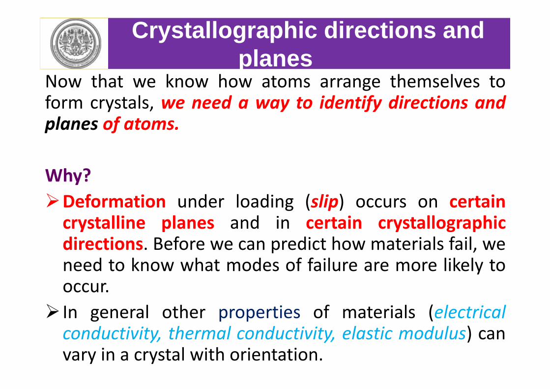
Now that we know how atoms arrange themselves toform crystals, we need a way to identify directions andplanes of atoms.
Why?Deformation under loading (slip) occurs on certaincrystalline planes and in certain crystallographicdirections. Before we can predict how materials fail, weneed to know what modes of failure are more likely tooccur.
In general other properties of materials (electricalconductivity, thermal conductivity, elastic modulus) canvary in a crystal with orientation.
Crystallographic directions and planes
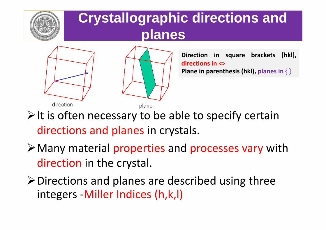
It is often necessary to be able to specify certain directions and planes in crystals.Many material properties and processes vary with direction in the crystal.Directions and planes are described using three integers ‐Miller Indices (h,k,l)
Crystallographic directions and planes
Direction in square brackets [hkl],directions in <>Plane in parenthesis (hkl), planes in
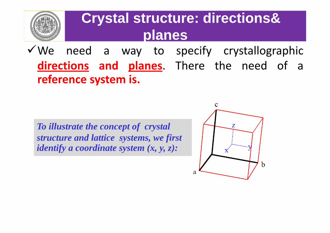
We need a way to specify crystallographicdirections and planes. There the need of areference system is.
Crystal structure: directions& planes
To illustrate the concept of crystal structure and lattice systems, we first identify a coordinate system (x, y, z):
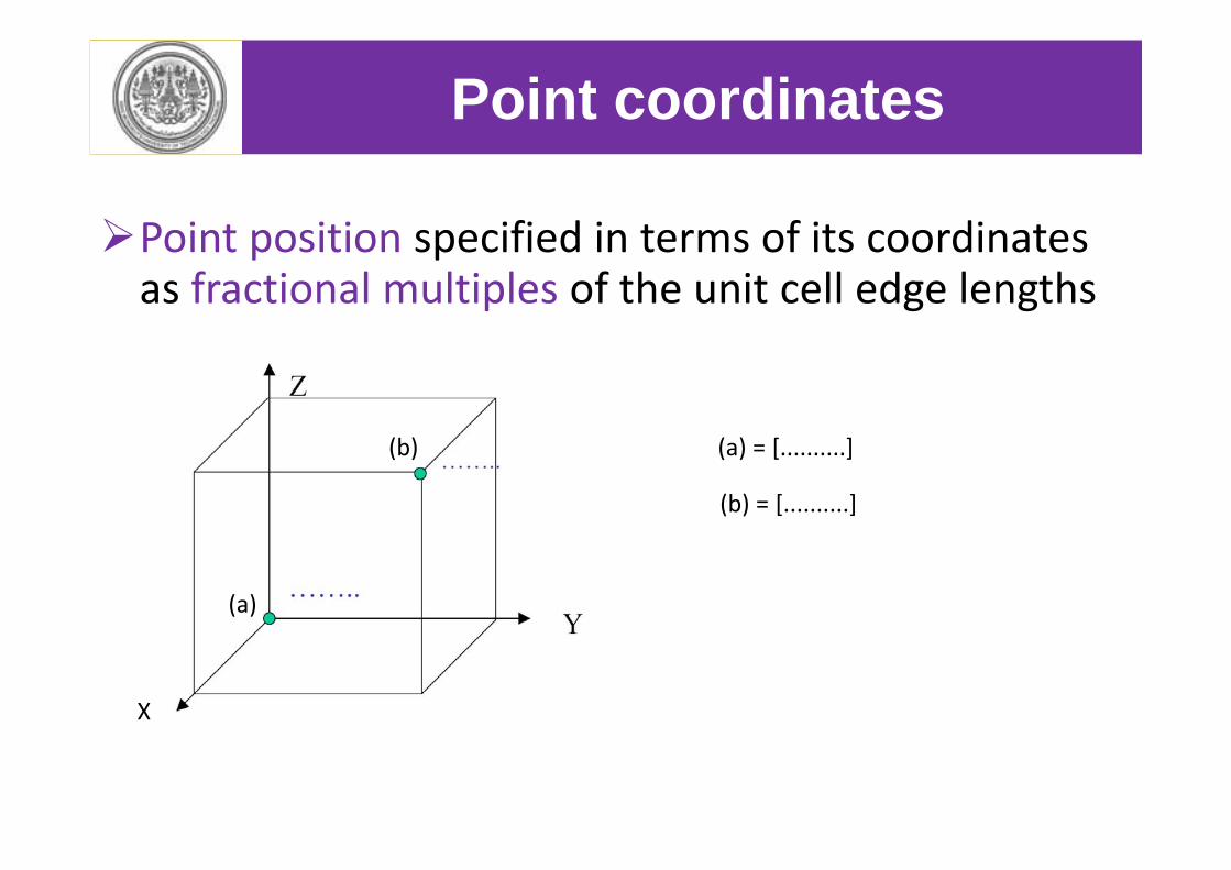
Point position specified in terms of its coordinates as fractional multiples of the unit cell edge lengths
Point coordinates
X
(b)
(a)
(a) = [..........]
(b) = [..........]
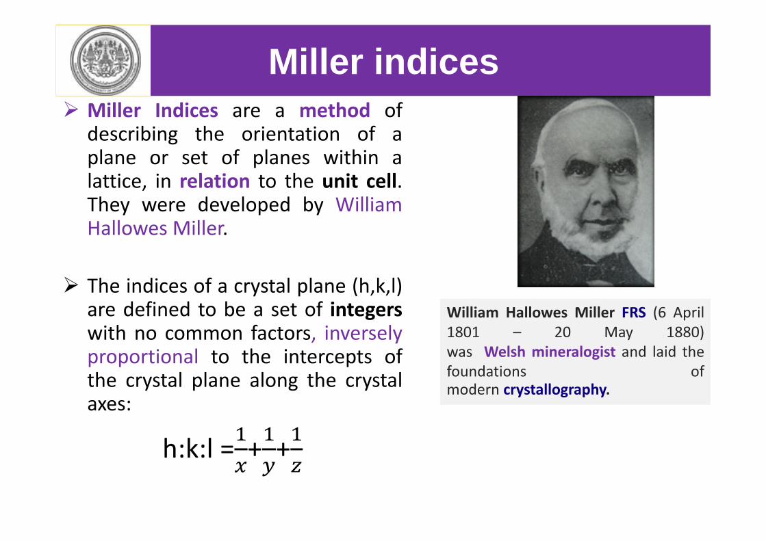
Miller Indices are a method ofdescribing the orientation of aplane or set of planes within alattice, in relation to the unit cell.They were developed by WilliamHallowes Miller.
The indices of a crystal plane (h,k,l)are defined to be a set of integerswith no common factors, inverselyproportional to the intercepts ofthe crystal plane along the crystalaxes:
h:k:l = + +
Miller indices
William Hallowes Miller FRS (6 April1801 – 20 May 1880)was Welsh mineralogist and laid thefoundations ofmodern crystallography.
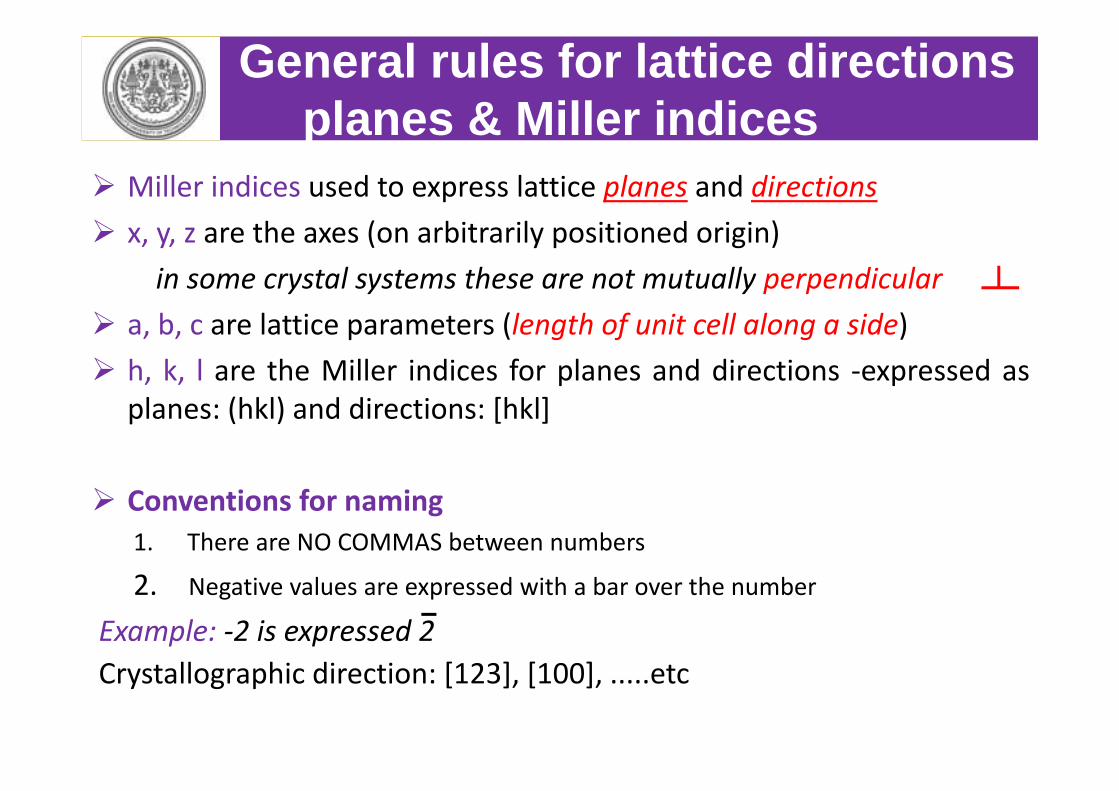
Miller indices used to express lattice planes and directions x, y, z are the axes (on arbitrarily positioned origin)
in some crystal systems these are not mutually perpendicular a, b, c are lattice parameters (length of unit cell along a side) h, k, l are the Miller indices for planes and directions ‐expressed as
planes: (hkl) and directions: [hkl]
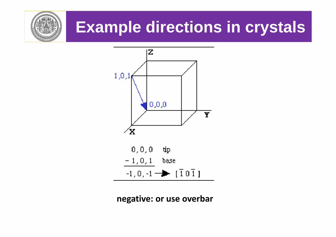
Conventions for naming1. There are NO COMMAS between numbers
2. Negative values are expressed with a bar over the number
Example: ‐2 is expressed 2Crystallographic direction: [123], [100], .....etc
General rules for lattice directions planes & Miller indices
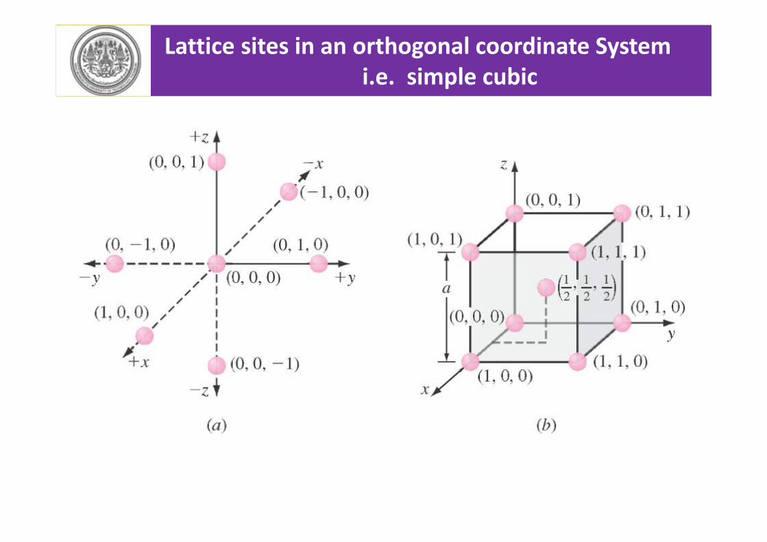
Lattice sites in an orthogonal coordinate Systemi.e. simple cubic
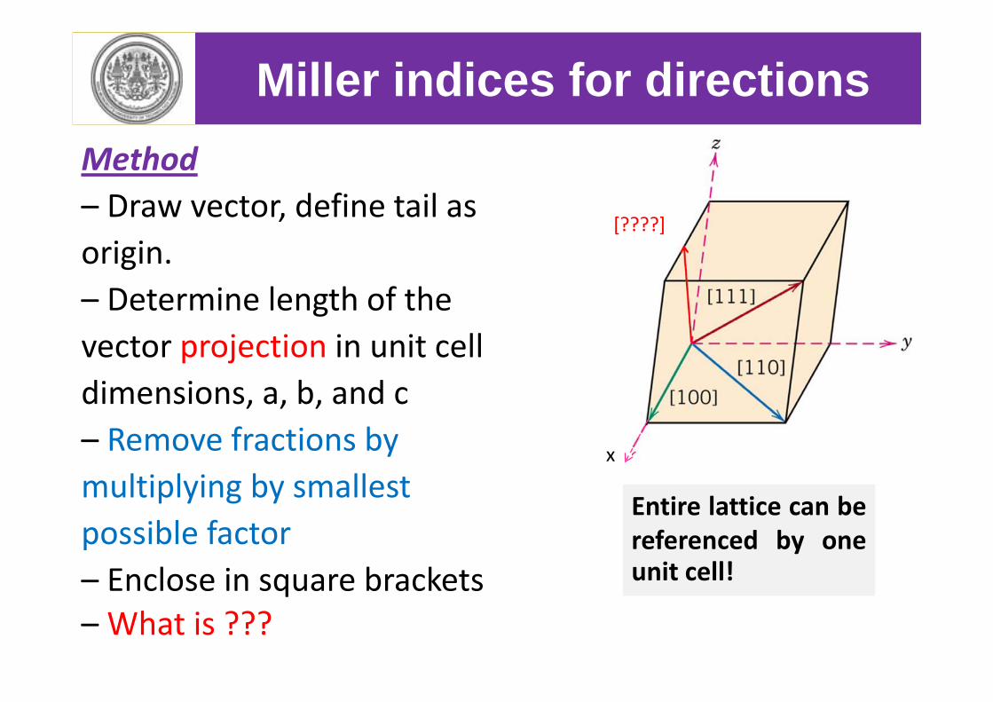
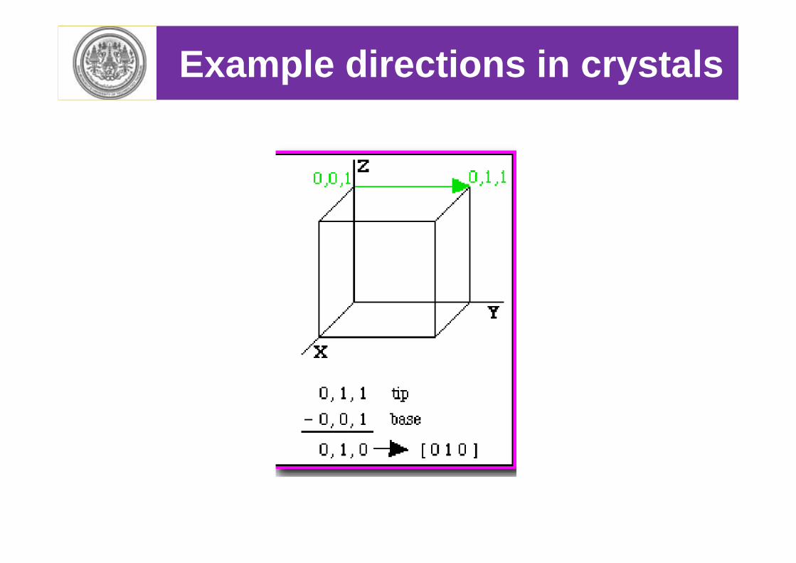
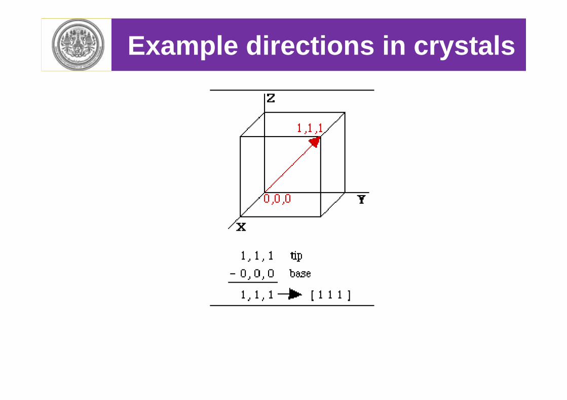
Method– Draw vector, define tail asorigin.– Determine length of thevector projection in unit celldimensions, a, b, and c– Remove fractions bymultiplying by smallestpossible factor– Enclose in square brackets– What is ???
Miller indices for directions
x
[????]
Entire lattice can bereferenced by oneunit cell!
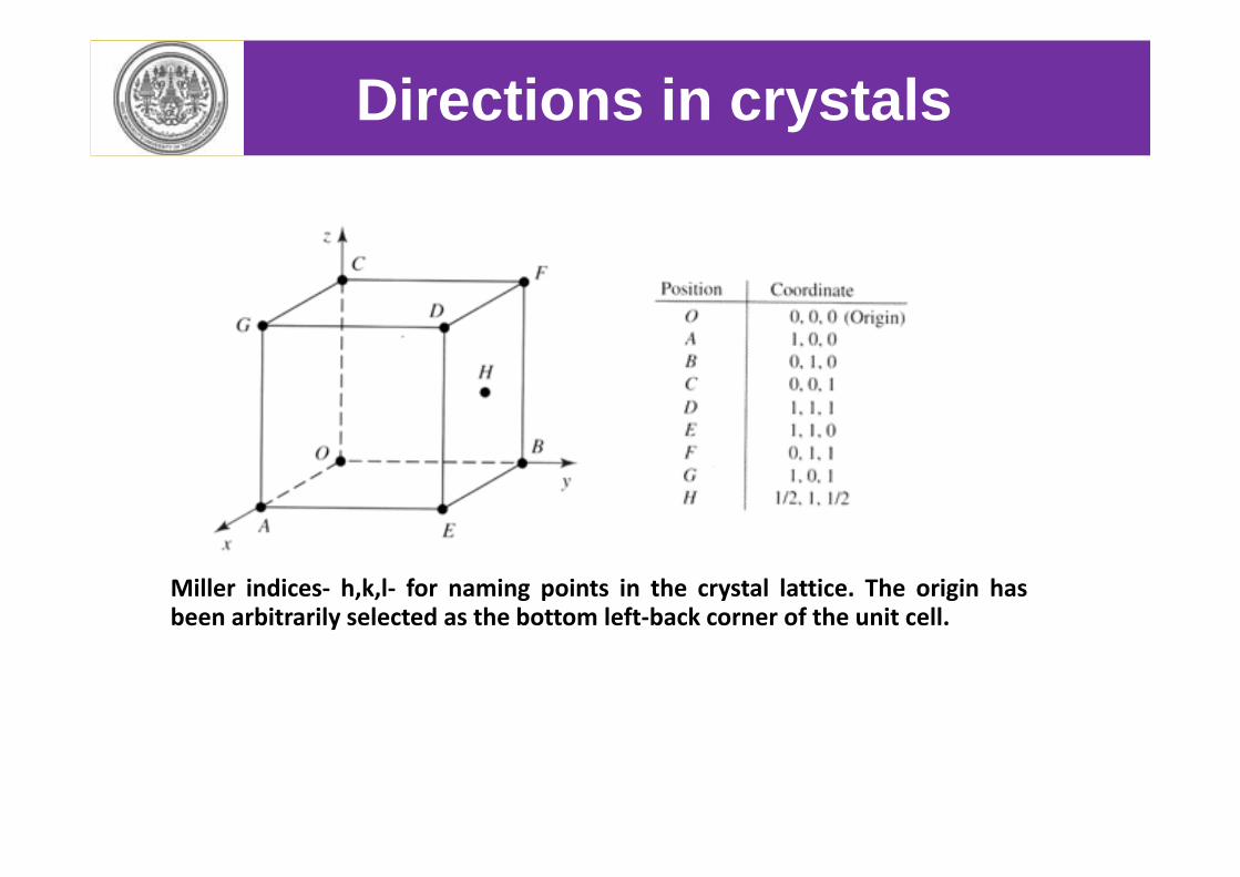
Directions in crystals
Miller indices‐ h,k,l‐ for naming points in the crystal lattice. The origin hasbeen arbitrarily selected as the bottom left‐back corner of the unit cell.
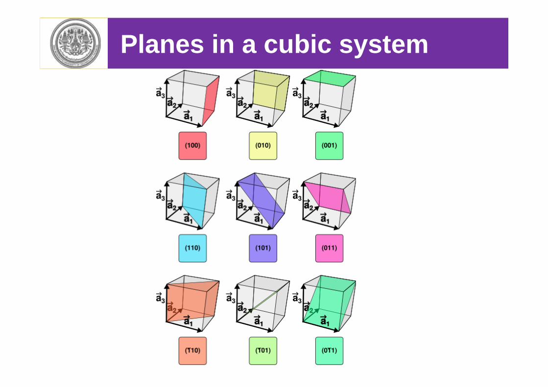
Planes in a cubic system
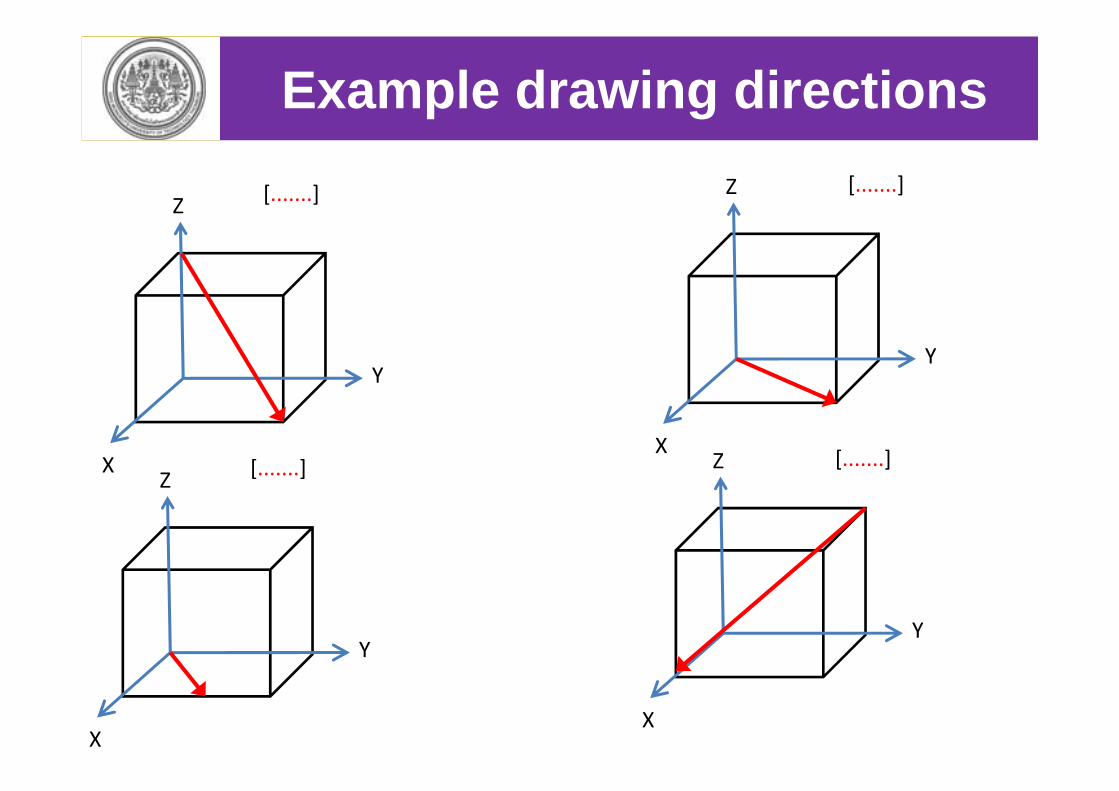
Example drawing directions
[.......]Z
Y
X
Z
Y
X
[.......]
[.......]Z
Y
X
Z
Y
X
[.......]
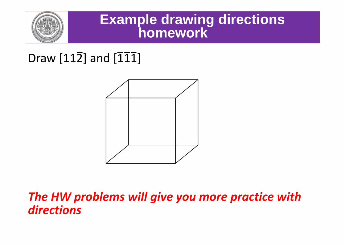
Draw [112] and [111]
The HW problems will give you more practice with directions
Example drawing directions homework
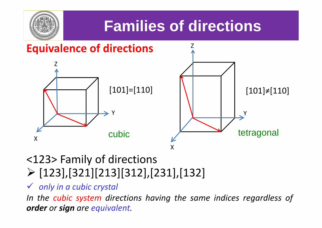
Equivalence of directions
Families of directions
Z
Y
X
Z
Y
X
<123> Family of directions [123],[321][213][312],[231],[132] only in a cubic crystalIn the cubic system directions having the same indices regardless oforder or sign are equivalent.
cubic tetragonal
[101]=[110] [101]≠[110]
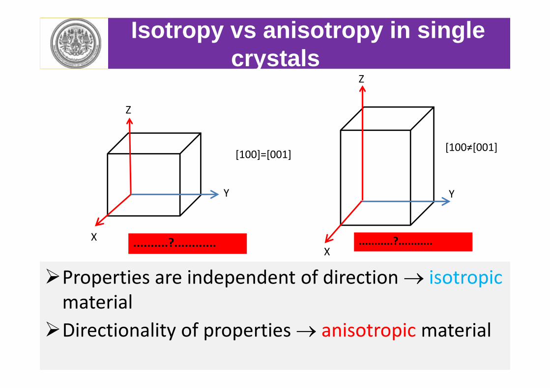
Properties are independent of direction isotropicmaterialDirectionality of properties anisotropic material
Isotropy vs anisotropy in single crystals
Z
Y
X
Z
Y
X
[100]=[001] [100≠[001]
..........?............ ...........?...........
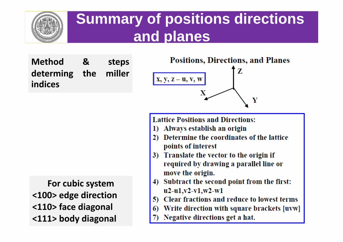
Summary of positions directions and planes
Method & stepsdeterming the millerindices
For cubic system <100> edge direction<110> face diagonal<111> body diagonal
Example directions in crystals
negative: or use overbar
Example directions in crystals
Example directions in crystals
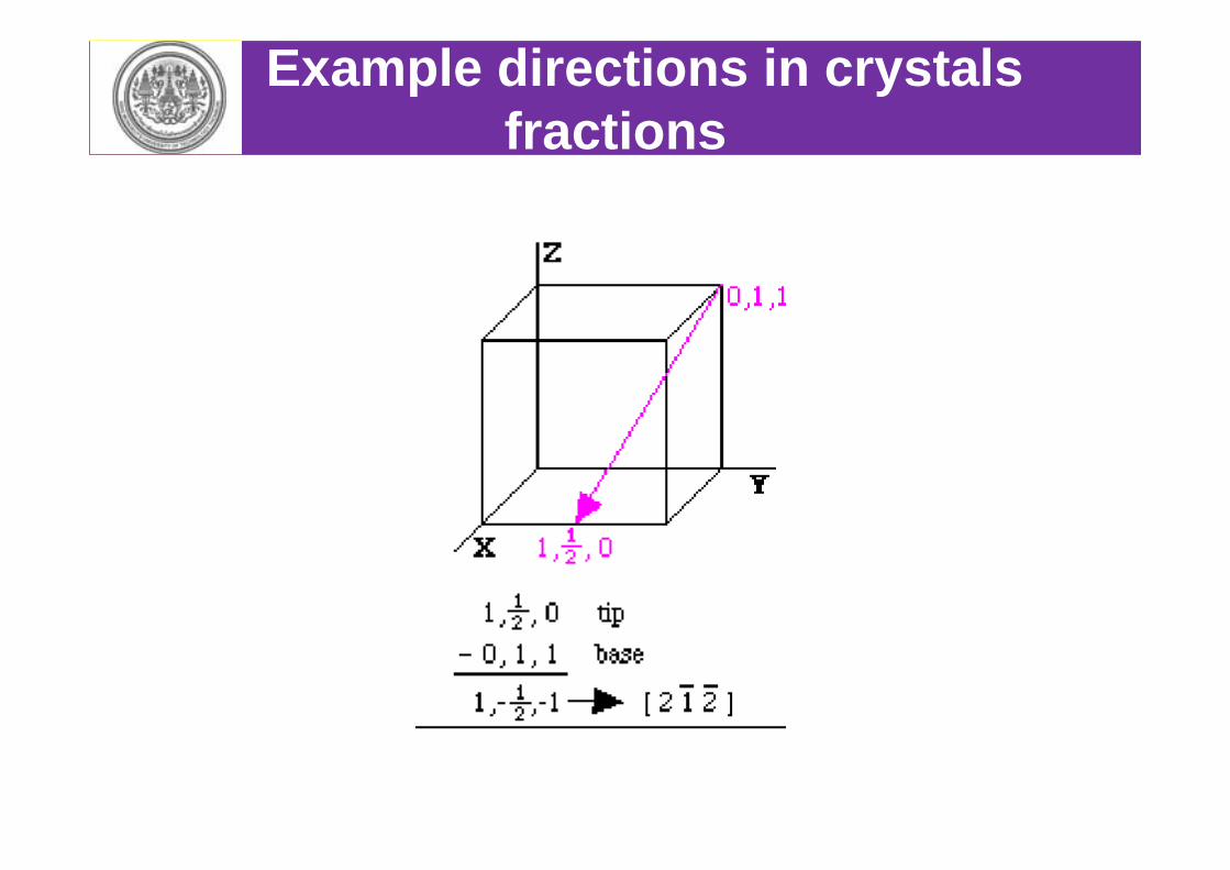
Example directions in crystalsfractions
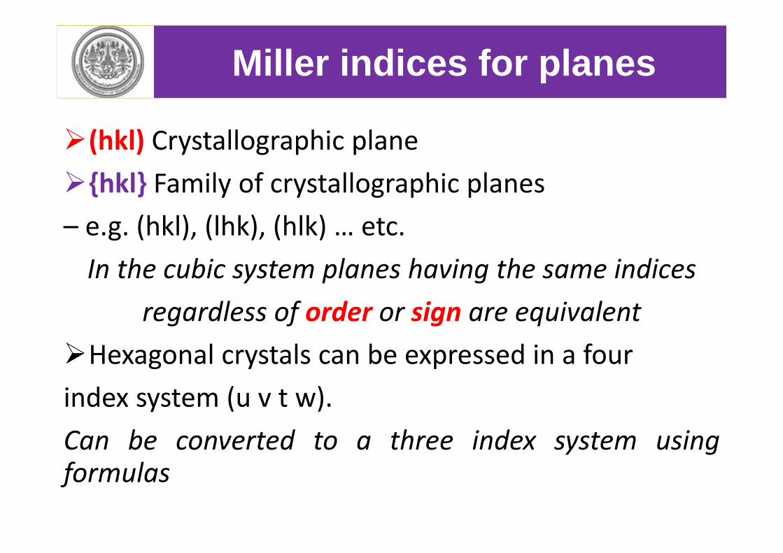
(hkl) Crystallographic plane{hkl} Family of crystallographic planes– e.g. (hkl), (lhk), (hlk) … etc.In the cubic system planes having the same indices
regardless of order or sign are equivalentHexagonal crystals can be expressed in a fourindex system (u v t w).Can be converted to a three index system usingformulas
Miller indices for planes
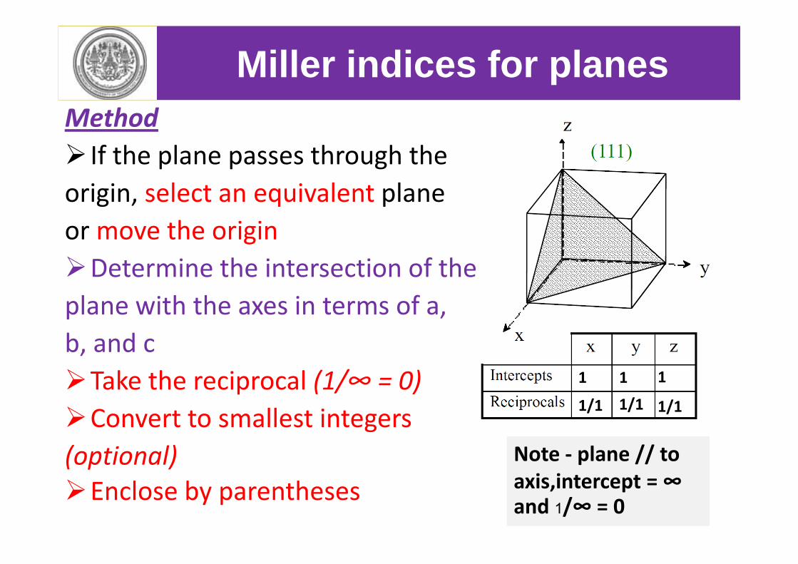
Method If the plane passes through theorigin, select an equivalent planeor move the originDetermine the intersection of theplane with the axes in terms of a,b, and cTake the reciprocal (1/∞ = 0)Convert to smallest integers(optional) Enclose by parentheses
Miller indices for planes
Note ‐ plane // to axis,intercept = ∞ and 1/∞ = 0
1 1 1
1/1 1/1 1/1
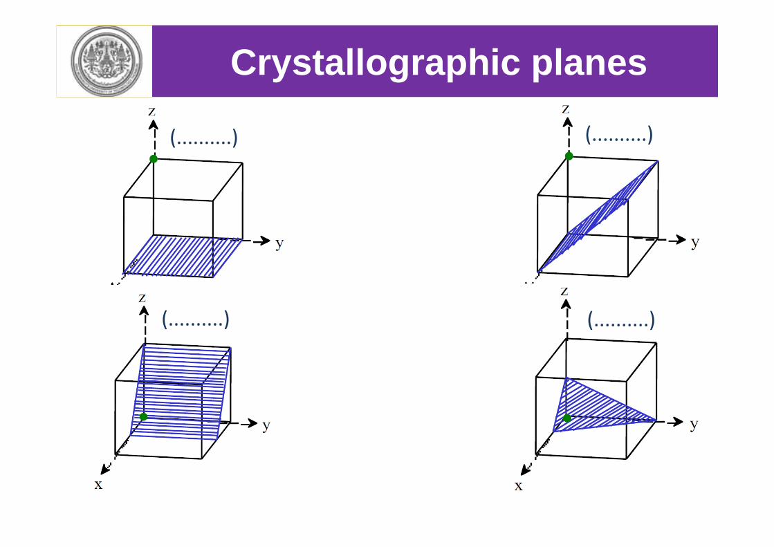
Crystallographic planes
(..........) (..........)
(..........) (..........)
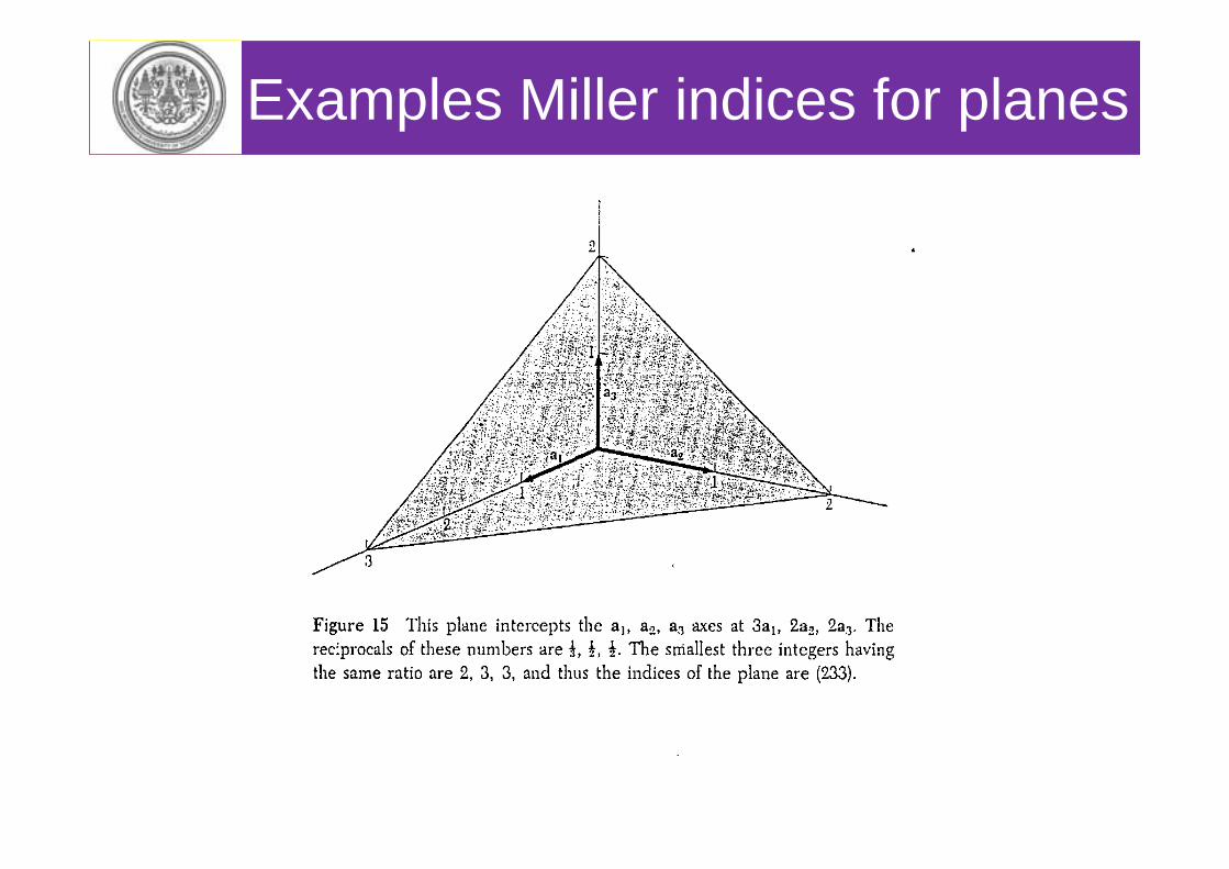
Examples Miller indices for planes
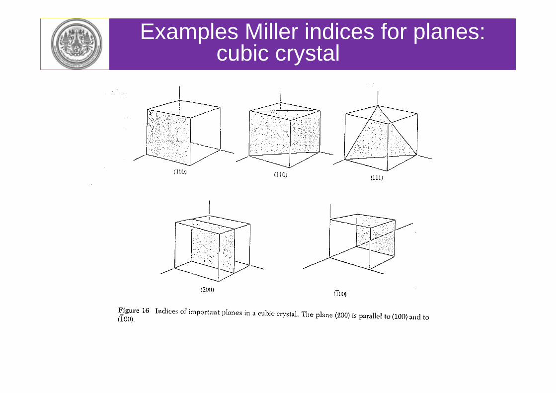
Examples Miller indices for planes: cubic crystal
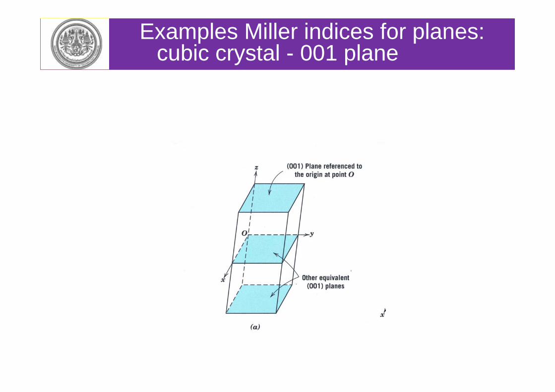
Examples Miller indices for planes: cubic crystal - 001 plane
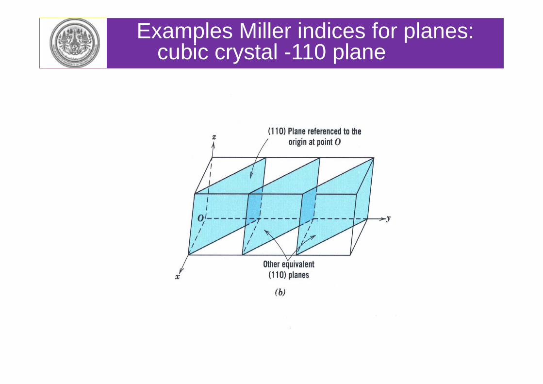
Examples Miller indices for planes: cubic crystal -110 plane
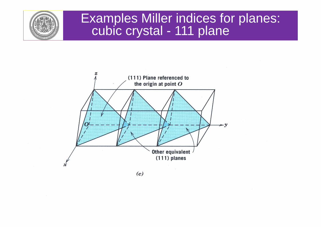
Examples Miller indices for planes: cubic crystal - 111 plane
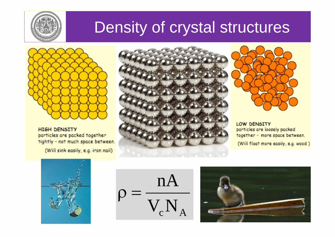
Density of crystal structures
AcNVnA
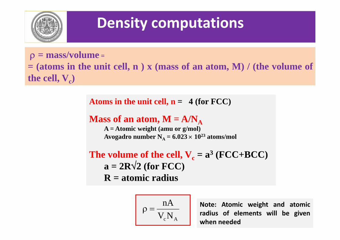
= mass/volume =
= (atoms in the unit cell, n ) x (mass of an atom, M) / (the volume ofthe cell, Vc)
Atoms in the unit cell, n = 4 (for FCC)
Mass of an atom, M = A/NAA = Atomic weight (amu or g/mol)Avogadro number NA = 6.023 1023 atoms/mol
The volume of the cell, Vc = a3 (FCC+BCC)a = 2R2 (for FCC)R = atomic radius
Density computations
AcNVnA
Note: Atomic weight and atomicradius of elements will be givenwhen needed
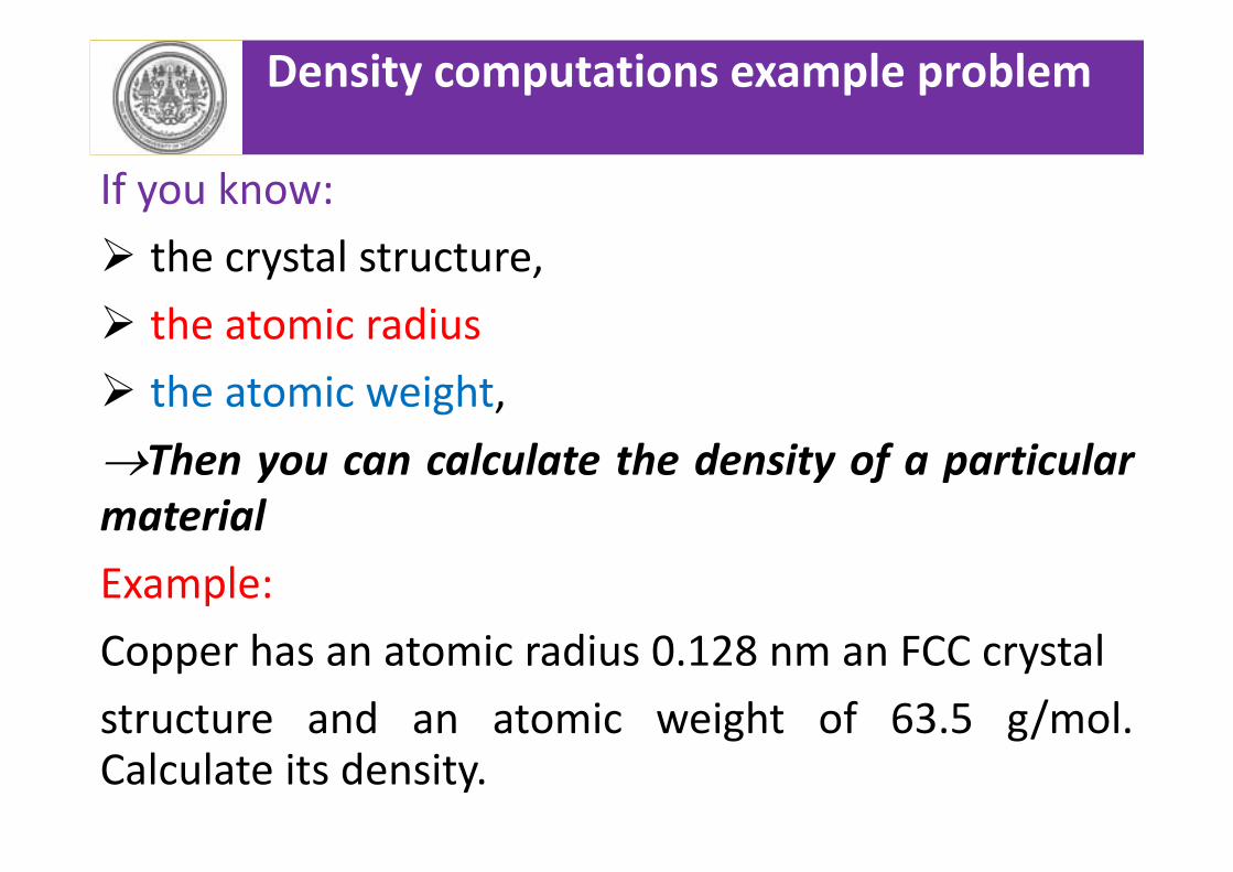
If you know: the crystal structure, the atomic radius the atomic weight,Then you can calculate the density of a particularmaterialExample:Copper has an atomic radius 0.128 nm an FCC crystalstructure and an atomic weight of 63.5 g/mol.Calculate its density.
Density computations example problem
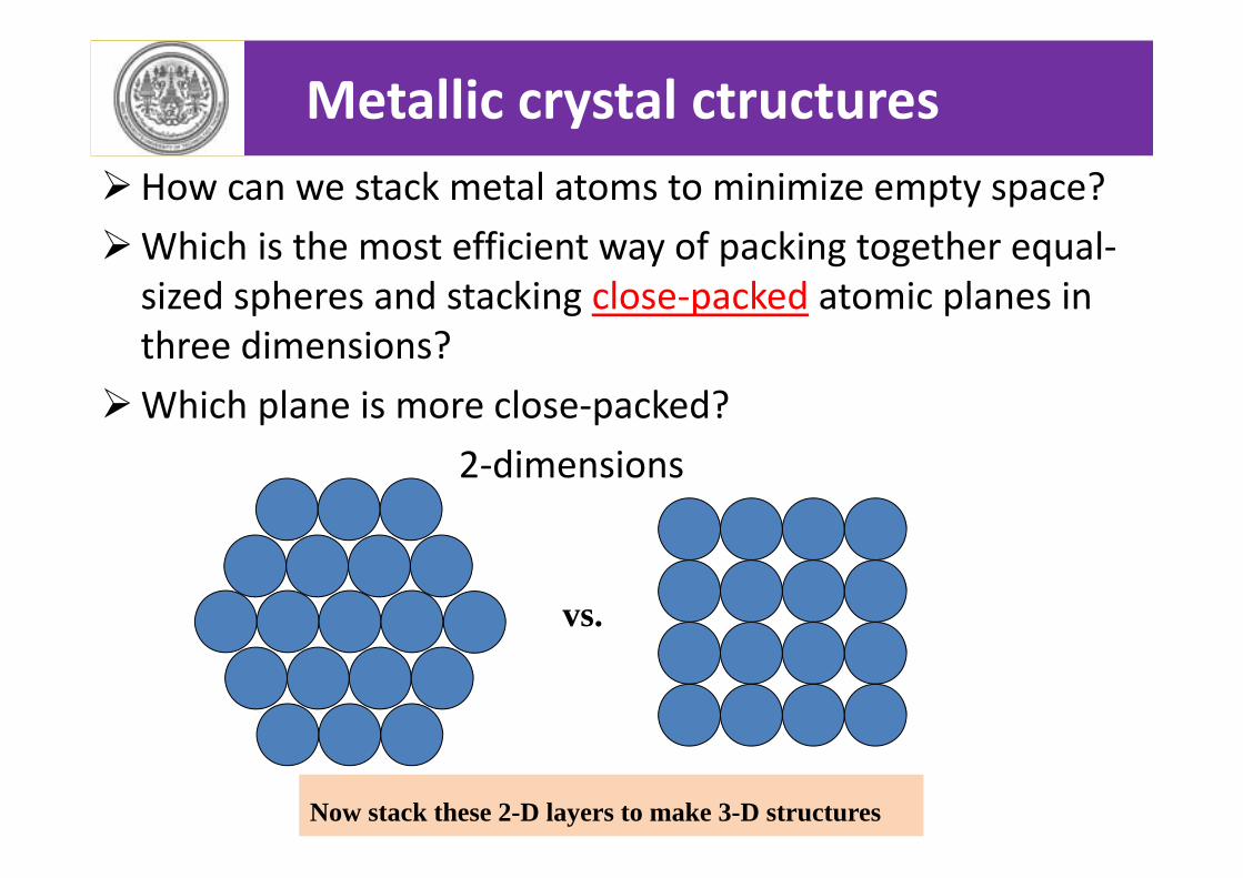
How can we stack metal atoms to minimize empty space?Which is the most efficient way of packing together equal‐sized spheres and stacking close‐packed atomic planes in three dimensions?
Which plane is more close‐packed? 2‐dimensions
vs.
Metallic crystal ctructures
Now stack these 2-D layers to make 3-D structures
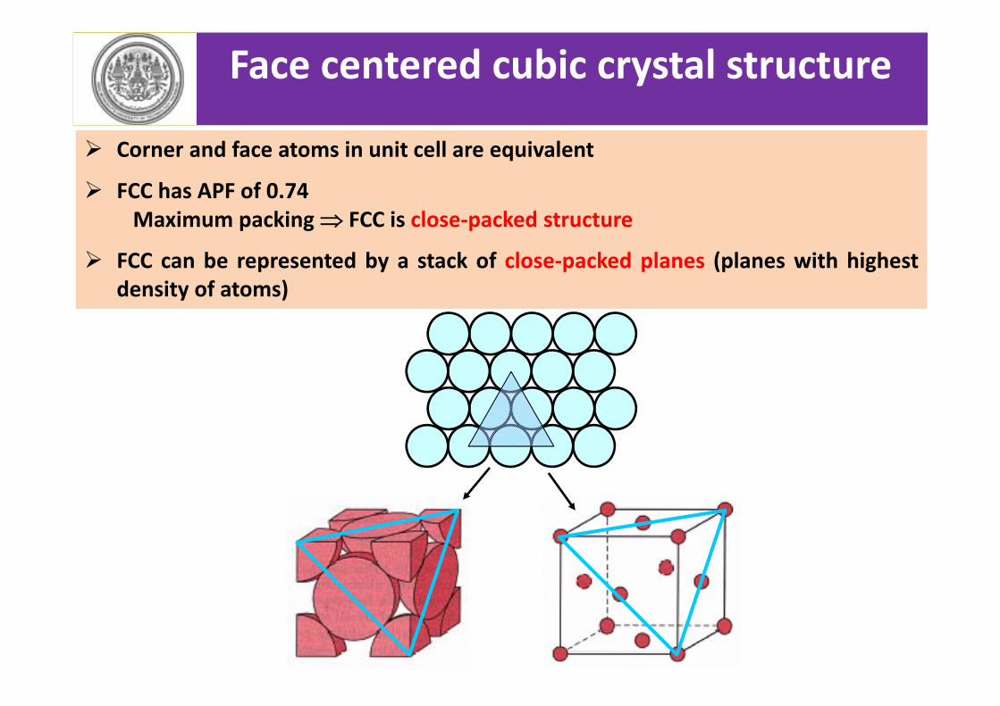
Corner and face atoms in unit cell are equivalent
FCC has APF of 0.74Maximum packing FCC is close‐packed structure
FCC can be represented by a stack of close‐packed planes (planes with highestdensity of atoms)
Face centered cubic crystal structure
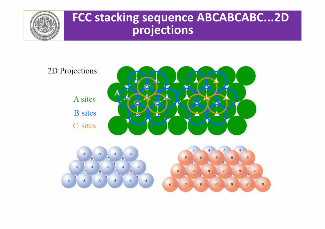
FCC stacking sequence ABCABCABC...2D projections
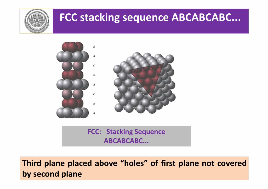
FCC: Stacking Sequence ABCABCABC...
Third plane placed above “holes” of first plane not coveredby second plane
FCC stacking sequence ABCABCABC...
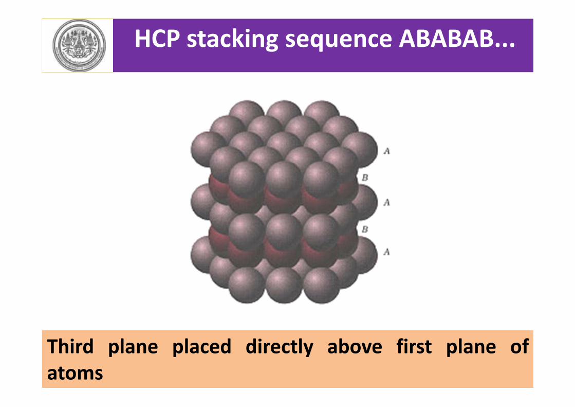
Third plane placed directly above first plane ofatoms
HCP stacking sequence ABABAB...
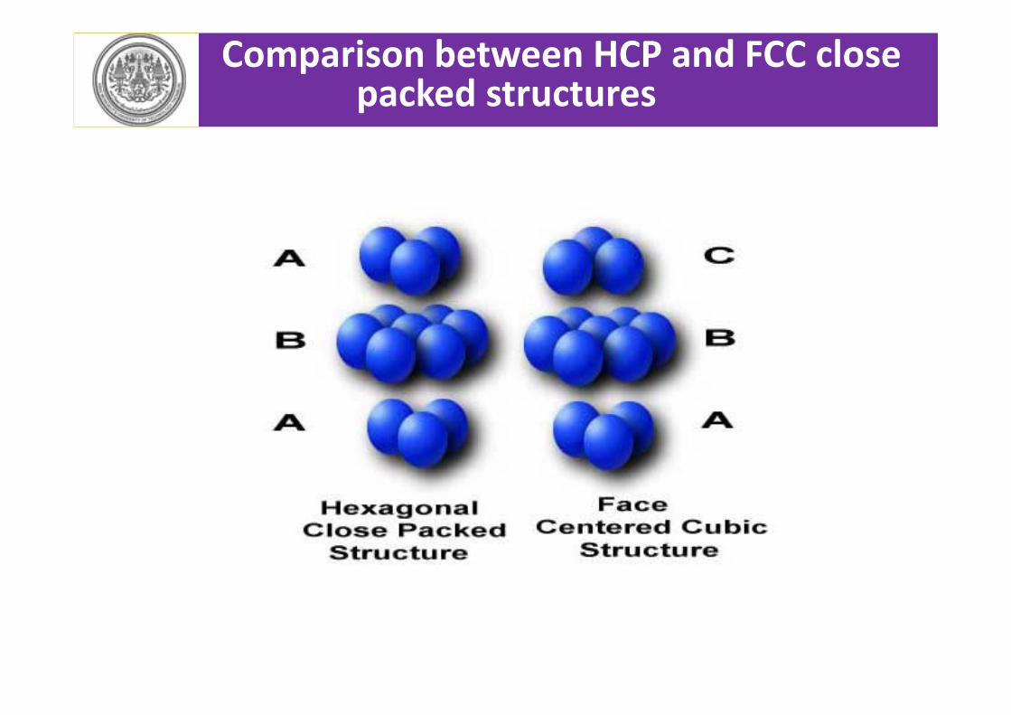
Comparison between HCP and FCC close packed structures
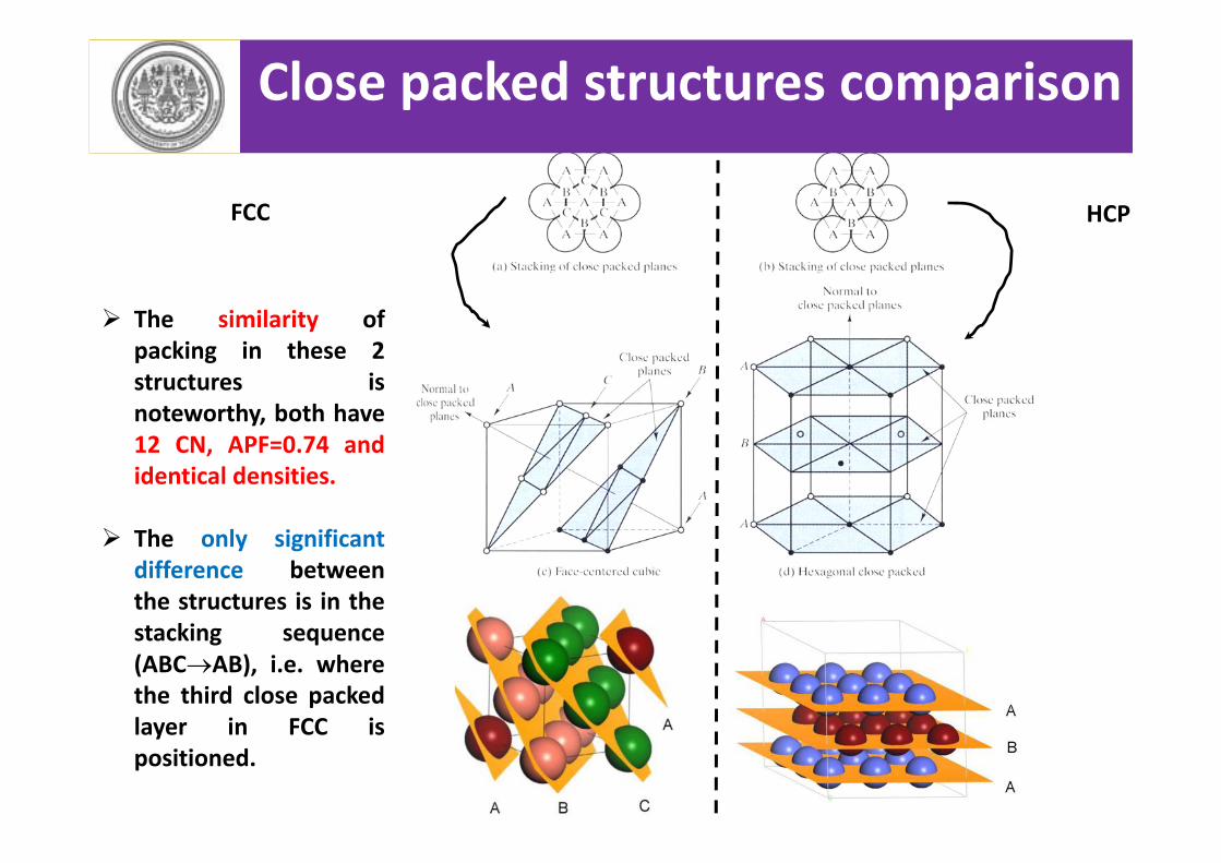
Close packed structures comparison
FCC HCP
The similarity ofpacking in these 2structures isnoteworthy, both have12 CN, APF=0.74 andidentical densities.
The only significantdifference betweenthe structures is in thestacking sequence(ABCAB), i.e. wherethe third close packedlayer in FCC ispositioned.
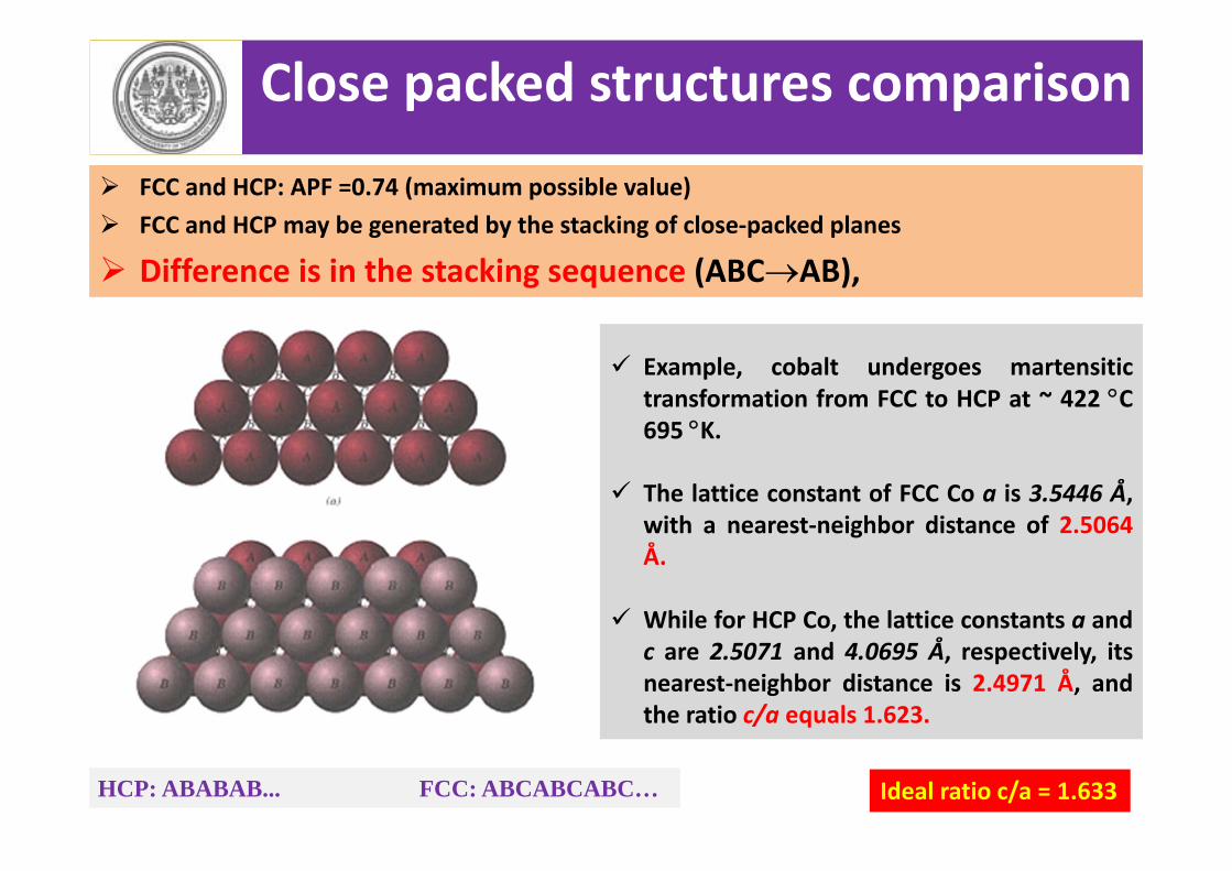
FCC and HCP: APF =0.74 (maximum possible value) FCC and HCP may be generated by the stacking of close‐packed planes
Difference is in the stacking sequence (ABCAB),
HCP: ABABAB... FCC: ABCABCABC…
Close packed structures comparison
Example, cobalt undergoes martensitictransformation from FCC to HCP at ~ 422 C695 K.
The lattice constant of FCC Co a is 3.5446 Å,with a nearest‐neighbor distance of 2.5064Å.
While for HCP Co, the lattice constants a andc are 2.5071 and 4.0695 Å, respectively, itsnearest‐neighbor distance is 2.4971 Å, andthe ratio c/a equals 1.623.
Ideal ratio c/a = 1.633
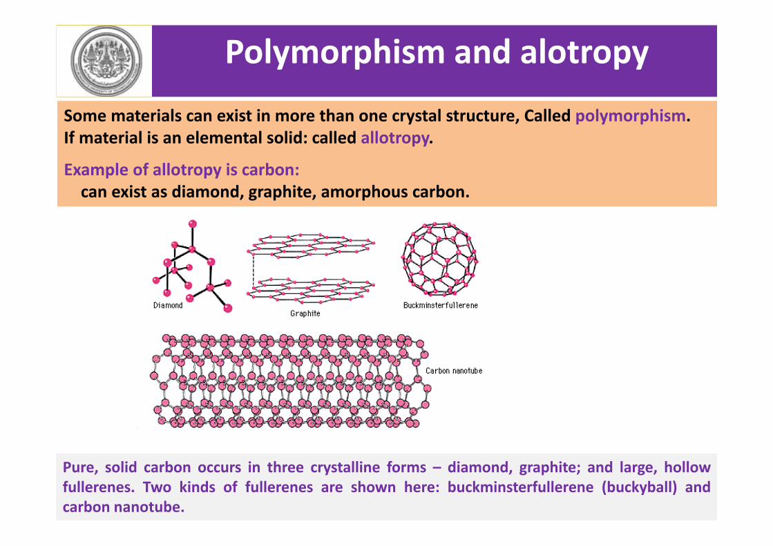
Some materials can exist in more than one crystal structure, Called polymorphism.If material is an elemental solid: called allotropy.
Example of allotropy is carbon:can exist as diamond, graphite, amorphous carbon.
Pure, solid carbon occurs in three crystalline forms – diamond, graphite; and large, hollowfullerenes. Two kinds of fullerenes are shown here: buckminsterfullerene (buckyball) andcarbon nanotube.
Polymorphism and alotropy
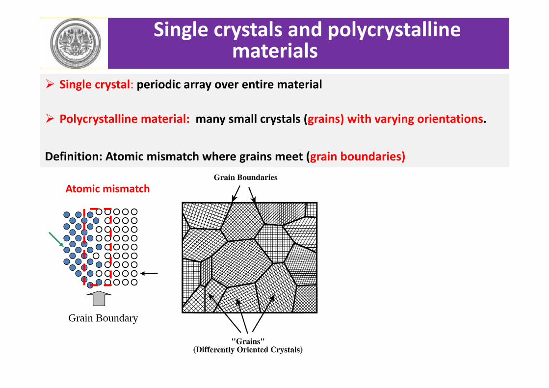
Single crystal: periodic array over entire material
Polycrystalline material: many small crystals (grains) with varying orientations.
Definition: Atomic mismatch where grains meet (grain boundaries)
Grain Boundary
Single crystals and polycrystalline materials
Atomic mismatch
Atomistic model of a nanocrystalline solid by Mo Li, JHU
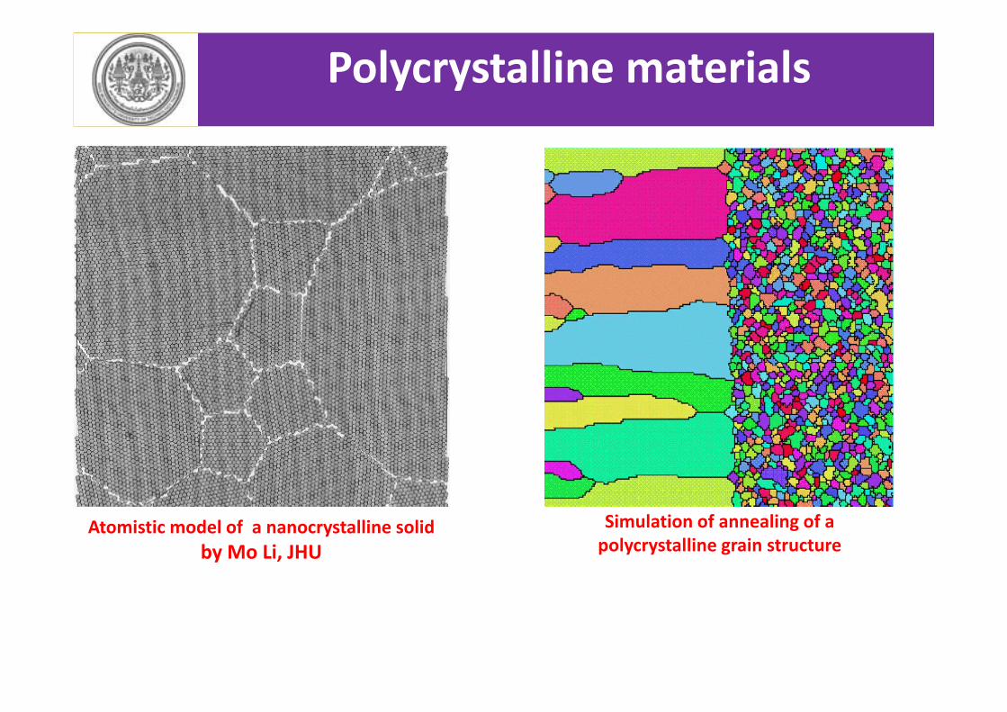
Polycrystalline materials
Simulation of annealing of a polycrystalline grain structure
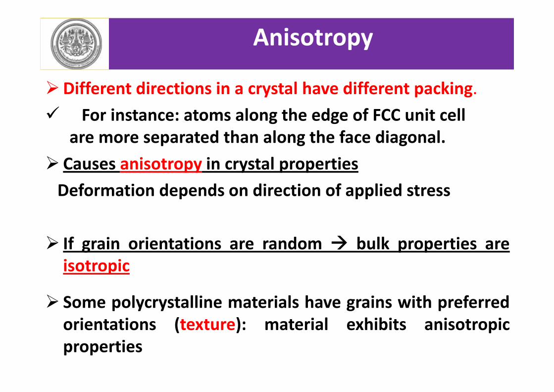
Different directions in a crystal have different packing. For instance: atoms along the edge of FCC unit cell
are more separated than along the face diagonal. Causes anisotropy in crystal propertiesDeformation depends on direction of applied stress
If grain orientations are random bulk properties areisotropic
Some polycrystalline materials have grains with preferredorientations (texture): material exhibits anisotropicproperties
Anisotropy
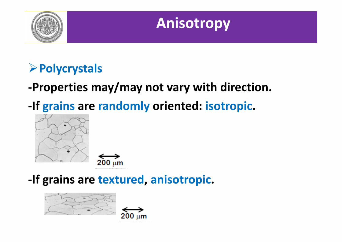
Polycrystals‐Properties may/may not vary with direction.‐If grains are randomly oriented: isotropic.
‐If grains are textured, anisotropic.
Anisotropy
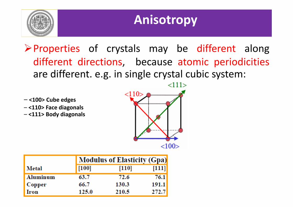
Properties of crystals may be different alongdifferent directions, because atomic periodicitiesare different. e.g. in single crystal cubic system:
Anisotropy
– <100> Cube edges– <110> Face diagonals– <111> Body diagonals
45
Allotropy Amorphous Anisotropy Atomic packing factor (APF) Body-centered cubic (BCC) Coordination number Crystal structure Crystalline Face-centered cubic (FCC) Hexagonal close-packed
(HCP) Isotropic Lattice parameter Non-crystalline Polycrystalline Polymorphism Single crystal Unit cell Miller indices
Make sure you understand language and concepts:
Summary

Questions?
Related Documents