Crystal Growth and Wafer Fabrication - Chapter 3 of Silicon VLSI Technology - Preparation of substrates - Czochralski (Cz) and Float Zone (FZ) techniques - Defects and Dopants - Measurement Techniques

Welcome message from author
This document is posted to help you gain knowledge. Please leave a comment to let me know what you think about it! Share it to your friends and learn new things together.
Transcript
Crystal Growth and Wafer Fabrication
- Chapter 3 of Silicon VLSI Technology
- Preparation of substrates
- Czochralski (Cz) and Float Zone (FZ) techniques
- Defects and Dopants
- Measurement Techniques

Why silicon?
We have discussed several reasons as to why silicon dominates:
band-gap ?????,
p-type and n-type dopants ???????,
SiO2 has many useful qualities ???????,
The raw material is very cheap (cost of one wafer?)
In defining substrates we need to specify:
1. Doping type/level,2. Crystal orientation,3. Impurity levels, (oxygen and carbon),4. Defect levels.


What makes a crystal?
-Crystals possess long-range order,
-We may have instead poly-crystalline or even amorphous material.
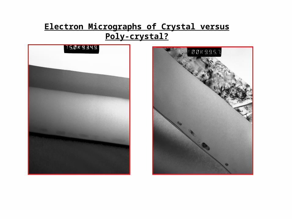
Electron Micrographs of Crystal versus Poly-crystal?
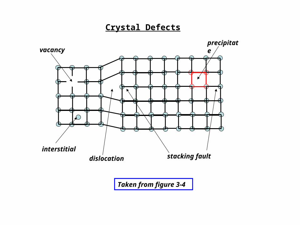
Crystal Defects
vacancy
interstitial
dislocation stacking fault
precipitate
Taken from figure 3-4
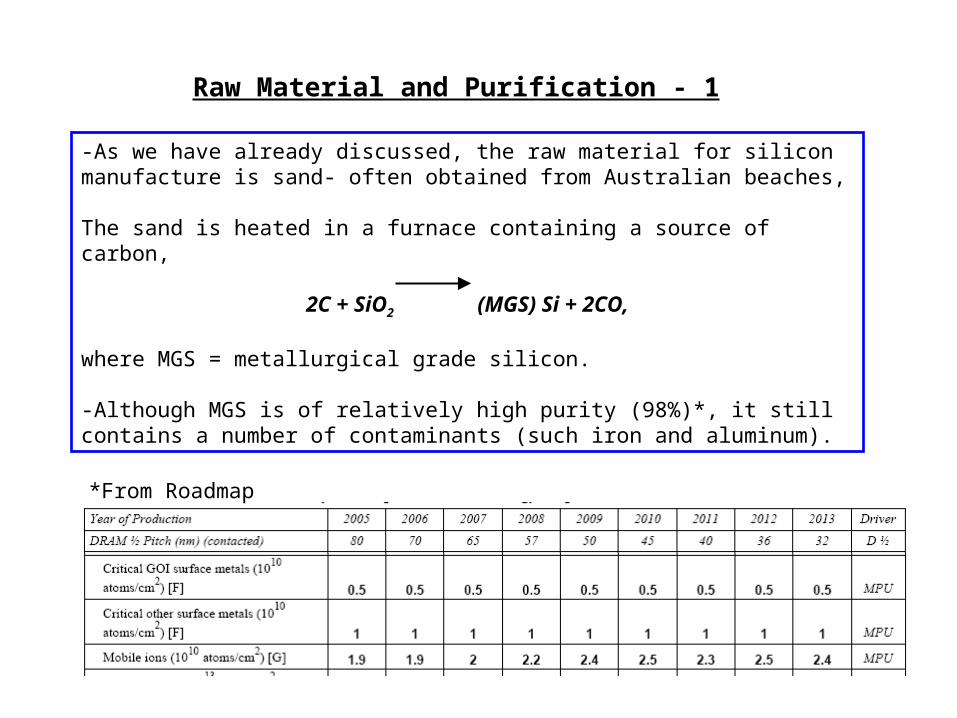
Raw Material and Purification - 1
-As we have already discussed, the raw material for silicon manufacture is sand- often obtained from Australian beaches,
The sand is heated in a furnace containing a source of carbon,
2C + SiO2 (MGS) Si + 2CO,
where MGS = metallurgical grade silicon.
-Although MGS is of relatively high purity (98%)*, it still contains a number of contaminants (such iron and aluminum).
*From Roadmap

Raw Material and Purification -2
-The MGS silicon is purified to EGS silicon (Electronic Grade Silicon) using a distillation process,
-First, the MGS is reacted with HCl to form SiHCl3, (trichlorosilane) which is in liquid form at room temperature,
-Fractional distillation results in impurity segregation, and extremely pure SiHCl3.
-To convert the SiHCl3 back into purified Si a CVD (Chemical Vapor Deposition) process is used (in a hydrogen atmosphere),
SiHCl3 (gas)+H2 (gas) 2Si (solid)+ 6HCl (gas),
-The nucleation surface is thin poly-Si rod, with a final thickness of many inches in diameter,-All that is specified is impurity level, so fast deposition is possible .

Wafer growth – Czochralski Method (Cz)
-From the high purity poly-Si, single crystal silicon is required,-The Cz process is the most common for large wafer diameter production.
-The EGS is broken into small pieces and placed in an SiO2 crucible,
-In an argon ambient, the crucible is heated to just above 1417oC,
-A single crystal seed is then lowered into the melt (crystal orientation and wafer diameter determined by seed orientation and pull rate),
-Dopant is added to the melt to intentionally dope the resulting crystal,
-The oxygen and carbon (from graphite furnace components), contribute about 1017-1018cm-3 contaminants.

Wafer growth – Float Zone (FZ)
-The Float Zone (FZ) growth method is far less common, and is reserved for situations where oxygen and carbon impurities cannot be tolerated,
-The entire poly-Si rod is extracted from the EGS process as a whole.
Poly-Si
c-Si
RF coil
-The rod is clamped at each end, with one end in contact with a single crystal seed,
-An RF heating coil induces currents in the silicon, heating it beyond its melting point.
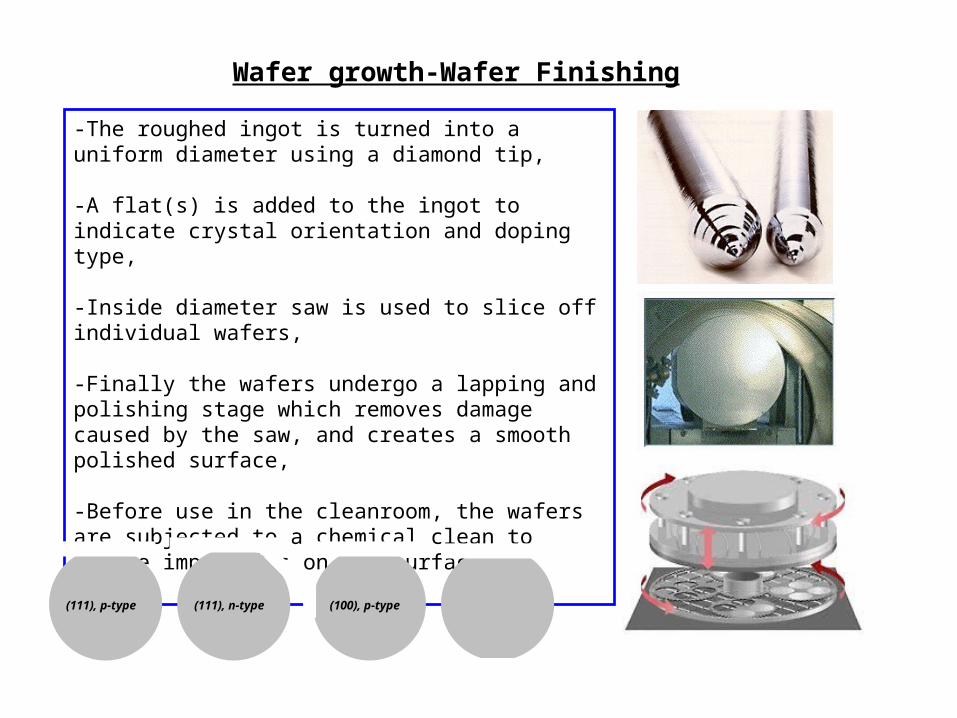
Wafer growth-Wafer Finishing
-The roughed ingot is turned into a uniform diameter using a diamond tip,
-A flat(s) is added to the ingot to indicate crystal orientation and doping type,
-Inside diameter saw is used to slice off individual wafers,
-Finally the wafers undergo a lapping and polishing stage which removes damage caused by the saw, and creates a smooth polished surface,
-Before use in the cleanroom, the wafers are subjected to a chemical clean to remove impurities on the surface.
(111), p-type (111), n-type (100), p-type
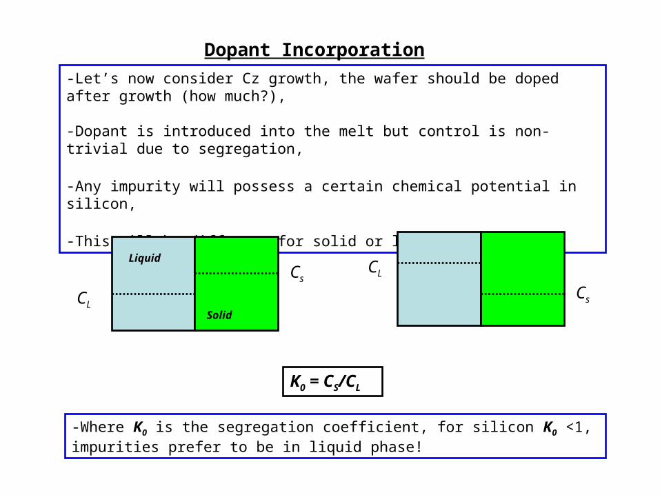
Dopant Incorporation
-Let’s now consider Cz growth, the wafer should be doped after growth (how much?),
-Dopant is introduced into the melt but control is non-trivial due to segregation,
-Any impurity will possess a certain chemical potential in silicon,
-This will be different for solid or liquid phases.
Cs
CLCs
CL
Solid
Liquid
K0 = CS/CL
-Where K0 is the segregation coefficient, for silicon K0 <1, impurities prefer to be in liquid phase!

Impurity k0
As 0.3
O 0.5
P 0.35
Sb 0.023
B 0.8
Au 0.000025
-We can relate the concentration of dopant in the solid crystal to the proportion of liquid and solid silicon by:
Cs = C0k0 (1-f)k0-1,
-where Cs is the concentration of dopant on the solid side of the interface, C0 is initial impurity concentration in the melt, and f is the ratio of solid silicon to the initial liquid volume,
-parameter of interest now in terms of known parameters!
-The concentration of impurity in the solid will change as a function of time, in other words, the distribution of dopant along the ingot will be graded.

Electrical Measurement Techniques – Hot Probe
Vm
HotCold
-The hot probe technique is used to determine the type of dopant in a wafer,
-It relies on the generation of the Seebeck voltage,
-i.e. the diffusion of free carriers as a result of a temperature gradient
e-
n-type wafer

Electrical Measurement Techniques – Four Point Probe
-The 4pp method measures the resistance of a wafer and using values of carrier mobility calculates the carrier concentration (why 4pp?),
-From geometry considerations we can show:
V= I/2rwhere r is the distance from the probe,
-in the case of 4pp this reduces to: = 2 s V/I,
which is valid if s<< t and d,
-in the case of wafers this can be reduced to:
= t/ln(2) V/I,-more conveniently:
= 1/ [q μp n + q μp p] - eqn. 1.1
V
I
St
d
= 4.532 V/I xj
s = 4.532 V/I
Bulk resistivity, cm
Sheet resistivity, /square

Electrical Measurement Techniques – Hall Effect
I
VH
B
e-
-Silicon is placed inside a magnetic field and a potential difference is placed across the material perpendicular to an applied electric field, the resultant motion of charge will experience a force perpendicular to the electric field,
-In equilibrium this results in a transverse potential difference known as the Hall voltage,
-The magnitude and sign of the Hall voltage leads directly to the carrier concentration, type, and mobility (if the resistivity is known).
RH = VH xj /B I
RH = 1/ qn (for n-type RH = μH
Hall coefficient
Giving Hall mobility
Related Documents