1 Creating a Wireless OBDII Scanner A Major Qualifying Report: Submitted to the Faculty Of the Worcester Polytechnic Institute In partial fulfillment of the requirements for the Degree of Bachelor of Science By _______________________________ Sean Mahoney _______________________________ John Keenan This 16 th day of October, 2008. Approved: ___________________________________ Professor Stephen J. Bitar, Advisor

Welcome message from author
This document is posted to help you gain knowledge. Please leave a comment to let me know what you think about it! Share it to your friends and learn new things together.
Transcript

1
Creating a Wireless OBDII Scanner
A Major Qualifying Report:
Submitted to the Faculty
Of the
Worcester Polytechnic Institute
In partial fulfillment of the requirements for the
Degree of Bachelor of Science
By
_______________________________
Sean Mahoney
_______________________________
John Keenan
This 16th day of October, 2008.
Approved:
___________________________________
Professor Stephen J. Bitar, Advisor

2

3
Abstract
This project consisted of the creation of a wireless On-Board Diagnostics scan tool which
implemented communications wirelessly. The main goal of the project was to be able to read
codes from a diagnostics port on a vehicle and report the codes wirelessly to a computer receiver.
The end result was a wireless communication device which utilized standard RS232 data
communication to send and receive codes.

4
Table of Contents
Abstract ........................................................................................................................................... 3
Table of Figures .............................................................................................................................. 5
Table of Tables ................................................................................................................................ 6
1 Background ............................................................................................................................. 7
1.1 The Clean Air Act............................................................................................................. 7
1.2 The Air Quality Act .......................................................................................................... 7
1.3 On-Board Diagnostics ...................................................................................................... 8
1.4 Standardization of On-Board Diagnostics ...................................................................... 10
1.5 Introduction of OBD-II ................................................................................................... 10
1.6 Types of OBD-II ............................................................................................................. 12
1.6.2 SAE J1850 ............................................................................................................... 14
1.6.3 Controller Area Networks ....................................................................................... 30
1.6.3.2 Message / Frame Types ........................................................................................... 32
1.6.3.3 Data Transmission Breakdown ............................................................................... 33
ISO 11519, Breband.net, CA� Information .......................................................................... 39
1.6.4 Implementation of OBD-II Protocols ...................................................................... 44
2 Project Definition .................................................................................................................. 46
2.1 Understanding Possible Target Markets ......................................................................... 46
2.1.1 AutoZone ................................................................................................................. 47
2.1.2 Emissions Testing Garages ..................................................................................... 48
2.2 Customer Requirements ................................................................................................. 50
2.3 Product Specifications .................................................................................................... 50
3 Product Design ...................................................................................................................... 51
3.1 System Flow ................................................................................................................... 51
3.1.1 Mobile Wireless Unit .............................................................................................. 51
3.1.2 Base Station Unit ..................................................................................................... 56
3.2 System Block Diagram ................................................................................................... 58
3.3 Hardware Assembly ....................................................................................................... 59
3.3.1 Final Hardware Purchase List ................................................................................. 59
3.3.2 Identification of Interfaces ...................................................................................... 63
4 Signal Representations .......................................................................................................... 64
4.1 OxBB................................................................................................................................... 65
4.2 Ox55 .................................................................................................................................... 66
5 Proof of Concept ................................................................................................................... 68
6 Recommendations ................................................................................................................. 68
5.1 Multiple Mobile Wireless Units ..................................................................................... 68
5.2 Scan Tool Implementation.............................................................................................. 69
6 Conclusions ........................................................................................................................... 70
Bibliography .................................................................................................................................. 72
5
Table of Figures
FIGURE 1 - TERMINAL IDENTIFICATION FOR ON BOARD DIAGNOSTICS PORT 9
FIGURE 2 – OBD-II FEMALE ADAPTER 11
FIGURE 3 - SAE J1850 VPW WAVEFORM 19
FIGURE 4 - J1850 MESSAGE 20
FIGURE 5 - J1850 MESSAGE HEADER FRAME 21
FIGURE 6 - SAE J1850 BIT SYMBOL TIMINGS 23
FIGURE 7 - PWM WAVEFORM EXAMPLES 26
FIGURE 8 - BIT DEFINITIONS FOR J1850 (VPW) 27
FIGURE 9 - J1850 VPW WAVEFORM USING PWM SIGNALS 29
FIGURE 10 - STANDARD FRAME BREAKDOWN, TEXAS INSTRUMENTS, I�TRODUCTIO� TO CA� 34
FIGURE 11 - EXTENDED FRAME BREAKDOWN, TEXAS INSTRUMENTS, I�TRODUCTIO� TO CA� 35
FIGURE 12 - CAN BIT TIMING DIAGRAM10 41
FIGURE 13 - CAN NETWORK IN PRACTICE2 42
FIGURE 14 - A VEHICLE NETWORK AND ITS COMPONENTS, DGTECH.COM, CONTROLLER AREA NETWORK 43
FIGURE 15 - LAYER PROTOCOL IN USE FOR THIS SYSTEM 45
FIGURE 16 - MOBILE WIRELESS UNIT BLOCK DIAGRAM 52
FIGURE 17 - MOBILE WIRELESS UNIT FINAL BLOCK DIAGRAM 53
FIGURE 18 - BASE STATION UNIT BLOCK DIAGRAM 57
FIGURE 19 - SYSTEM BLOCK DIAGRAM 59
FIGURE 20 - ARDUINO PIN CONFIGURATION 63
FIGURE 21 - XBEE SHIELD 64
FIGURE 22 - 0XBB SIGNAL (THEORY) 65
FIGURE 23 - 0XBB SIGNAL (PRACTICE) 66
FIGURE 24 - 0X55 SIGNAL (THEORY) 67

6
FIGURE 25 - 0X55 SIGNAL (PRACTICE) 67
Table of Tables
TABLE 1 - J1850 PROTOCOL OPTIONS(VALENTINE, 1998) ........................................................................................... 15
TABLE 2 - NON-DESCRIPT SAMPLE COMMUNICATIONS PROTOCOL .............................................................................. 17
TABLE 3 - PROTOCOL INCORRECTLY DEFINED............................................................................................................. 18
TABLE 4 - CAN MESSAGE TYPES ................................................................................................................................ 33
TABLE 5 - STANDARD FRAME BIT DEFINITONS............................................................................................................ 35
TABLE 6 - EXTENDED FRAME BIT DEFINITIONS ........................................................................................................... 36
TABLE 7 - SO 11898, BREDBAND.NET, CAN INFORMATION ........................................................................................ 39
TABLE 8 - ISO 11519, BREBAND.NET, CAN INFORMATION ......................................................................................... 39
TABLE 9 - BUS LENGTH VS MAXIMUM BIT RATE, BREBAND.NET, CAN INFORMATION ................................................ 40

7
1 Background
1.1 The Clean Air Act
Over the span of the 20th century, citizens of the United States have witnessed the birth and
growth of one of today’s largest industries, the automotive industry. By 1960 the number of
automobiles on the road rose to over 74 million and would continue to rise throughout the
decade. Originally identified by Congress’s Air Pollution Act of 1955, Congress acknowledged
that air pollution may result in major harm to the public welfare from personal health to national
health of the country and with a 25 million dollar grant "An Act to provide research and
technical assistance relating to air pollution control" was executed.
After eight years The Public Health Service’s research concluded the necessity for a standardized
form of regulation by local and state governments in order to protect the well being of the public.
In 1963, Congress passed The Clean Air Act, "An Act to improve, strengthen, and accelerate
programs for the prevention and abatement of air pollution." Exhaust from these vehicles was the
largest factor in their pollution and would soon result in national emission standards. Another
major influence to the amount of pollution was the oil being used which of contained high levels
of sulfur, the Clean Air Act mandated that research and development would remove the sulfur
from the fuels being used.
1.2 The Air Quality Act
A major stepping stone came in 1967 with the Air Quality Act. This Act divided the United
States into Air Quality Control Regions in an effort to monitor ambient air. With continued

8
research, the 1970 Clean Air Act, "An Act to amend the Clean Air Act to provide for a more
effective program to improve the quality of the Nation's air," was put into effect.
President Richard Nixon formed the Environmental Protection Agency (EPA) in the interest to
protect human health and the United States’ air, water, and land. Under the 1970 Clean Air Act,
the EPA received thirty million dollars to develop and enforce emission standards and
regulations to minimize airborne contaminants such as those made by engine combustion; Sulfur
Oxides, Carbon Dioxides, Hydrocarbons, and Nitrogen Oxides. The EPA developed minimal
regulations of all 1975 models to emit 90% less Hydrocarbons and Carbon Monoxide in
comparison to those of 1970 models. Nitrogen Oxides would be given until 1976 models to be
reduced by 90%. To make sure the Automotive Industry was adhering to the newly formed
emission regulations the EPA enforced an enormous ten thousand dollar fine for every vehicle
built that did not meet specifications. From 1975 through 1980 the EPA worked hand in hand
with the Automotive Industry and continuously granted extensions in an effort to lower
Hydrocarbons and Carbon Monoxide.
1.3 On-Board Diagnostics
A milestone for automotive efficiency arrived in the forms of On-board computers On-Board
Diagnostics, OBD, beginning in 1980. These computers would monitor the fuel injection
systems and would have simple capabilities and adjustments, in return, were the start of
something great to come. The General Motors Company became the first to build an interface in
their vehicle in 1982, the Assembly Line Communications Link. By 1986, the ALCL, known as
the ALDL, Assembly Line Diagnostic Link, seen below in Figure 1 - Terminal Identification for

9
On Board Diagnostics Port, had developed into a much better system where the problem with
inconsistency in communication links had been resolved with the implementation of The
Universal Asynchronous Receiver/Transmitter.
The original On Board Diagnostic interface included twelve input bays, nine of which were
connected to a line of some sort. Each line had a specific function and communicated utilizing a
non standard protocol. A drawing representation of the original on board diagnostics port can be
found in Figure 1.
Figure 1 - Terminal Identification for On Board Diagnostics Port1
1 Robert Powers Motorsports - http://robertpowersmotorsports.freeservers.com/images/ALDL_plug.jpg
10
1.4 Standardization of On-Board Diagnostics
Throughout the growth of emission standards and regulations, the state of California was the
backbone for many of the changes that took place. The California Air Resource Board (CARB)
enforced that all new vehicles that would be sold in California in 1988 would have an On-Board
Diagnostic system incorporated. This became known as OBD-I. In an effort to clean the air, the
CARB anticipated that by monitoring the vehicles overall efficiency by enforcing yearly
emissions testing, the public would desire vehicles that would more reliably pass inspection.
Unfortunately, due to the lack of standardization of the emissions tests and the variety of OBD-I
systems from different manufactures, the annual emissions testing was a long way from where it
needed to be to enforce the public’s vehicles to meet any regulations. In collaboration with the
EPA, CARB conducted an OBD-I case study.
1.5 Introduction of OBD-II
California again led the emissions standards into the next era after six years of on board
diagnostics research. The next generation diagnostics interface was called OBD-II. All new
vehicles sold in California after 1996 are required to meet OBD-II specifications and standards.
OBD-II is a result of the years of research and development by the Society of Automotive
Engineers (SAE), the CARB and the EPA. Incorporating OBDIs positive aspects, these
engineers developed a system that would be standardized throughout the country in an effort to
successfully enforce emissions standards.
11
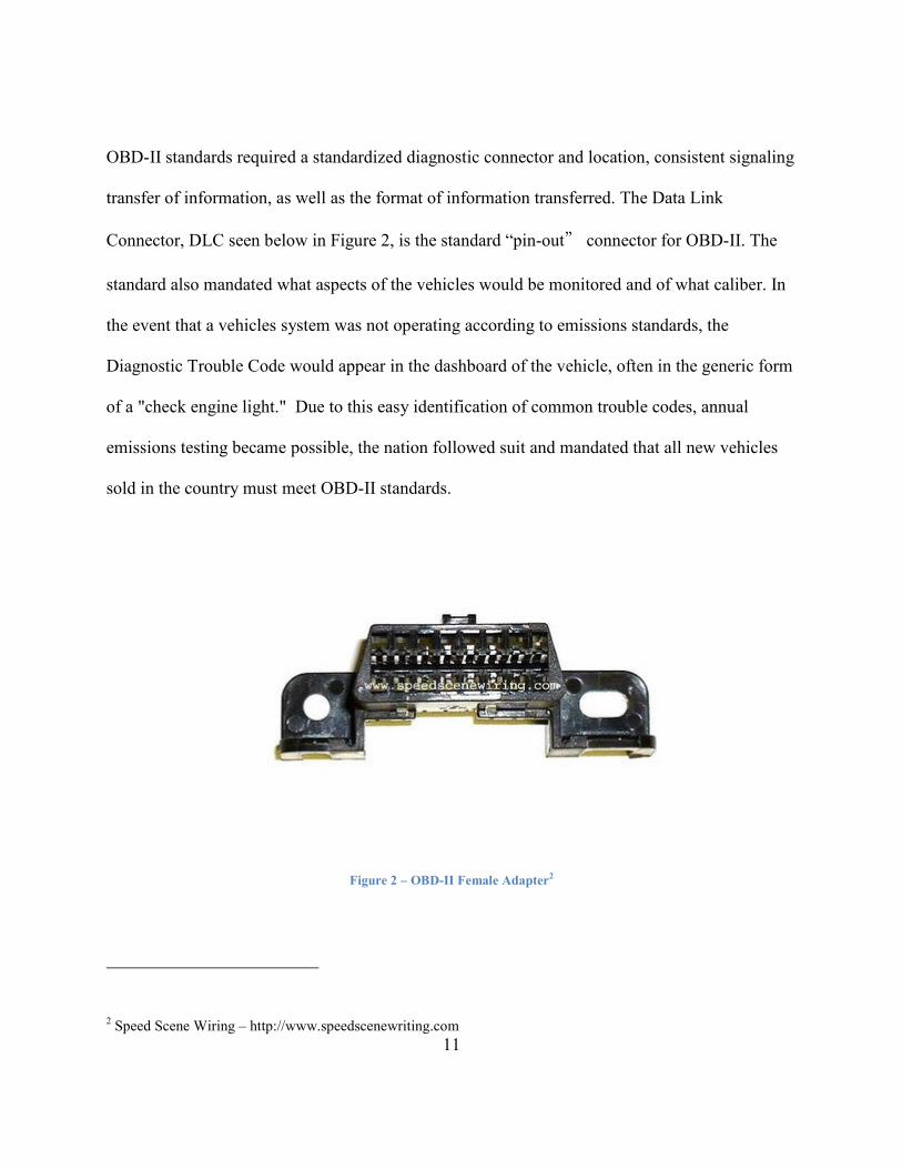
OBD-II standards required a standardized diagnostic connector and location, consistent signaling
transfer of information, as well as the format of information transferred. The Data Link
Connector, DLC seen below in Figure 2, is the standard “pin-out” connector for OBD-II. The
standard also mandated what aspects of the vehicles would be monitored and of what caliber. In
the event that a vehicles system was not operating according to emissions standards, the
Diagnostic Trouble Code would appear in the dashboard of the vehicle, often in the generic form
of a "check engine light." Due to this easy identification of common trouble codes, annual
emissions testing became possible, the nation followed suit and mandated that all new vehicles
sold in the country must meet OBD-II standards.
Figure 2 – OBD-II Female Adapter2
2 Speed Scene Wiring – http://www.speedscenewriting.com

12
1.6 Types of OBD-II
There are three types of OBD-II. The first, and oldest standard, is ISO 9141-2. This standard
was defined by the International Organization for Standardization in 1989 in response to the
California Air Resources Board’s call for cleaner emissions.
The second standard was standardized by the Society of Automotive Engineers. The
standardization defined is the SAE J1850 Communications Standard. This standard can be
implemented in one of two ways. The implementation occurs through Variable Pulse Width
(VPW), or Pulse-Width Modulation (PWM).
Recent improvements in automobiles require more computing power distributed around the
vehicle. Due to this increased number of nodes which need to communicate, a newer, faster bus
speed is needed. Further investigation brought CAN, or Controller Area Network, into focus,
and all vehicles sold in the United States after 2008 are required to implement this standard of
communications.
1.6.1 ISO 9141-2
The ISO 9141-2 protocol is based on serial communication using one of two lines. Pin 7 and Pin
15 are the two lines of communication, and are labeled K line and L line, respectively. Serial
communication transfers bits using high and low voltages to represent bits, 0, or low, is
represented by a zero volt message, 1, or high, is represented by 12 volts.

13
Communication through ISO 9141-2 is asynchronous and has a data transfer speed of 10.4
kBaud. Data bits have a maximum high to low propagation delay of 2 microseconds. Similarly,
the maximum low to high propagation delay is also 2 microseconds.
This protocol is framed with a certain set of data which includes a header byte, a set of data
bytes, and a checksum byte. The frame is the same as the J1850 messages, and follows the same
message format. The difference lies in the physical architecture.
ISO 9141-2 has a similar protocol to RS-232. The K line is the communication wire, and the L
line is used solely for “waking up” the unit, and is optional and useless other than for this
particular function. The unit can, in fact, be woken up utilizing the K line, which makes the L
line somewhat obsolete.
1.6.1.1 ISO 9141-2 Signaling
The K line of the ISO 9141-2 bus idles high, and is drawn down with messaging. A specific
UART is used in the communication, although not at RS-232 voltage levels. High voltage is set
at the voltage of the battery.
The message frames are signaled to look the exact same as the J1850 protocol, but is restricted to
12 bytes. There includes a header byte, message body, and an end byte.
The ISO 9141-2 standard operates at a frequency of 10,400 bits per second. Because this is a
fixed period, there is no consideration for bit timing. Bits are represented by the line’s state and
the line’s state only. When the line is “high,” the bit is equal to 1, when the line is “low,” the bit

14
is equal to 0. Consecutive bits which are the same cause no edge on the line and the line will
continue at that value.
1.6.1.2 Initiation Protocol
Connecting to an ISO 9141 capable OBD-II port requires a sequence of handshaking steps in
order to communicate. The process3 is as follows:
1. Select the K line from the OBD-II wiring harness to use as Serial Communications
2. Set outgoing communication to 5 baud
3. Transmit a hex value of 0x33h to the OBD-II Port
4. Immediately set incoming/outgoing communications to 10400 baud
5. The line is now half duplex and the OBD-II Port should echo 0x33h
6. A response from the OBD-II will read 0x55h
Since this was the first standard put into place for OBD-II communication, it is somewhat limited
in its functionality. There is no error checking available to programmers and it is the slowest
type of communication. The communication between the OBD-II scan tool and the OBD-II port
is very structured and cannot be interrupted. Once a command is sent, the sender must wait for a
response from the receiver.
1.6.2 SAE J1850
The SAE J1850 standard was a recommended standard for seven years before being officially
adopted by the Society of Automotive Engineers in February, 1994.4 The standard which has
come to be known as SAE J1850 is a Class B classification. There are two types of pulse
3 Software Development - http://www.obd.dk/sw.htm 4 Oliver, D. John: Implementing the J1850 Protocol – Intel Corporation
15
modulation. Frequency Division Multiplexing, which transmits two or more messages
simultaneously on a single channel, and Time division multiplexing, which interleaves two or
more signals on the same channel for either a fixed or a variable length of time.
1.6.2.1 J1850 Implementation Types
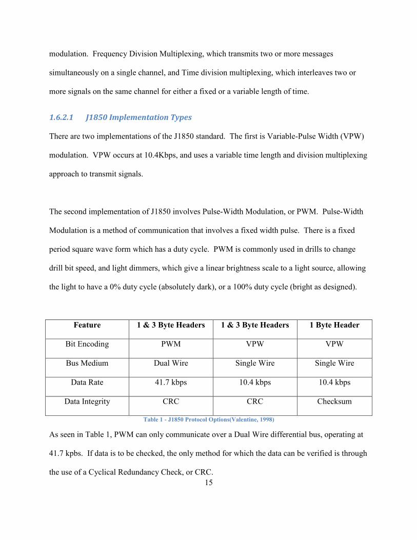
There are two implementations of the J1850 standard. The first is Variable-Pulse Width (VPW)
modulation. VPW occurs at 10.4Kbps, and uses a variable time length and division multiplexing
approach to transmit signals.
The second implementation of J1850 involves Pulse-Width Modulation, or PWM. Pulse-Width
Modulation is a method of communication that involves a fixed width pulse. There is a fixed
period square wave form which has a duty cycle. PWM is commonly used in drills to change
drill bit speed, and light dimmers, which give a linear brightness scale to a light source, allowing
the light to have a 0% duty cycle (absolutely dark), or a 100% duty cycle (bright as designed).
Feature 1 & 3 Byte Headers 1 & 3 Byte Headers 1 Byte Header
Bit Encoding PWM VPW VPW
Bus Medium Dual Wire Single Wire Single Wire
Data Rate 41.7 kbps 10.4 kbps 10.4 kbps
Data Integrity CRC CRC Checksum
Table 1 - J1850 Protocol Options(Valentine, 1998)
As seen in Table 1, PWM can only communicate over a Dual Wire differential bus, operating at
41.7 kpbs. If data is to be checked, the only method for which the data can be verified is through
the use of a Cyclical Redundancy Check, or CRC.
16
1.6.1.3 PWM Explained
PWM is an anagram for Pulse-Width Modulation, where a signal is generated having a particular
duty cycle, but always the same period. Put simply, a signal generator must, at a particular
frequency, draw the line high for a certain percentage of the period, known as the “duty cycle.”
PWM is particularly useful when only one voltage is available, yet a variable voltage deliver is
needed. PWM is explained further later in this paper, but it is traditionally used in power drills
for construction to change speeds, light dimmers in homes, and “servo’s,” which spin to a
particular angle when given a signal with the associated duty cycle.
PWM relates to OBD-II because it is the encoding scheme of choice for all 41.7 kbps J1850
implementations. This standard uses two lines for communication, and one for reference to
ground. Pins 2 and 10 are used for the communications, while standard voltages and ground are
used from the OBD-II connector.
The protocol employs multiple checks to ensure data integrity, such as Carrier Sense Multiple
Access (CMSA). CMSA is a protocol in which nodes on a network sense and verify the absence
of data and other traffic before beginning a transmission of its own.
It further employs a CRC, which is a polynomial division explained later in this document. With
all of these features, PWM communications proves to be a very unique, solid protocol which can
be trusted for one-bus communications.
17
1.6.2.2 VPW Explained
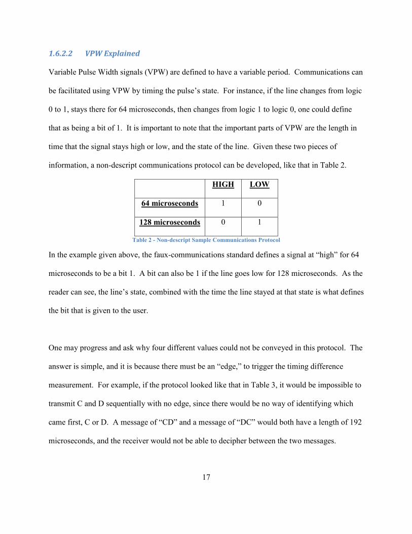
Variable Pulse Width signals (VPW) are defined to have a variable period. Communications can
be facilitated using VPW by timing the pulse’s state. For instance, if the line changes from logic
0 to 1, stays there for 64 microseconds, then changes from logic 1 to logic 0, one could define
that as being a bit of 1. It is important to note that the important parts of VPW are the length in
time that the signal stays high or low, and the state of the line. Given these two pieces of
information, a non-descript communications protocol can be developed, like that in Table 2.
HIGH LOW
64 microseconds 1 0
128 microseconds 0 1
Table 2 - 1on-descript Sample Communications Protocol
In the example given above, the faux-communications standard defines a signal at “high” for 64
microseconds to be a bit 1. A bit can also be 1 if the line goes low for 128 microseconds. As the
reader can see, the line’s state, combined with the time the line stayed at that state is what defines
the bit that is given to the user.
One may progress and ask why four different values could not be conveyed in this protocol. The
answer is simple, and it is because there must be an “edge,” to trigger the timing difference
measurement. For example, if the protocol looked like that in Table 3, it would be impossible to
transmit C and D sequentially with no edge, since there would be no way of identifying which
came first, C or D. A message of “CD” and a message of “DC” would both have a length of 192
microseconds, and the receiver would not be able to decipher between the two messages.

18
HIGH LOW
64 microseconds A C
128 microseconds B D
Table 3 - Protocol Incorrectly Defined
VPW is the encoding scheme of choice for all 10.4Kbaud J1850 implementations. The standard
uses one line for communications and one ground reference line. The communication line is
defined to be Pin 2 on the OBD-II connector, and the ground reference line is one of the two
ground types, Chassis Ground on Pin 4, or Signal Ground on Pin 5. Signal high, known as an
Active bit, or logic 1, is represented by +7 volts. Under +3.5 v is defined as a Passive Bit, signal
low, or logic 0.
VPW communicates on the data bus via time dependent symbols. More specifically, a “high” bit
is not necessarily a high potential on the bus. Through VPW communications, a “one” or “high”
bit is a symbol denoted by a transition on the bus that lasts for some fixed amount of time. The
amount of time that the bus stays at a particular potential is the determination of which “bit” is
being transferred.
19
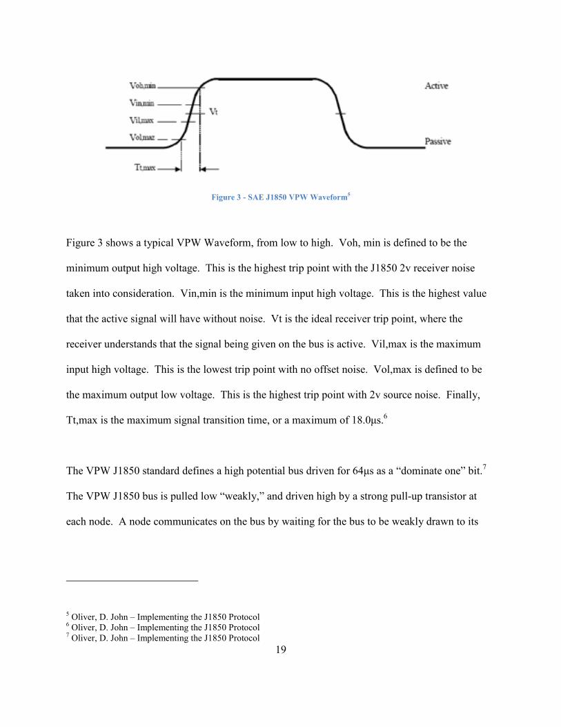
Figure 3 - SAE J1850 VPW Waveform5
Figure 3 shows a typical VPW Waveform, from low to high. Voh, min is defined to be the
minimum output high voltage. This is the highest trip point with the J1850 2v receiver noise
taken into consideration. Vin,min is the minimum input high voltage. This is the highest value
that the active signal will have without noise. Vt is the ideal receiver trip point, where the
receiver understands that the signal being given on the bus is active. Vil,max is the maximum
input high voltage. This is the lowest trip point with no offset noise. Vol,max is defined to be
the maximum output low voltage. This is the highest trip point with 2v source noise. Finally,
Tt,max is the maximum signal transition time, or a maximum of 18.0µs.6
The VPW J1850 standard defines a high potential bus driven for 64µs as a “dominate one” bit.7
The VPW J1850 bus is pulled low “weakly,” and driven high by a strong pull-up transistor at
each node. A node communicates on the bus by waiting for the bus to be weakly drawn to its
5 Oliver, D. John – Implementing the J1850 Protocol 6 Oliver, D. John – Implementing the J1850 Protocol 7 Oliver, D. John – Implementing the J1850 Protocol
20
low potential at ground, or it can drive the bus to a high potential of approximately 7.5v with the
node’s pull-up transistor.
The SAE J1850 standard defines a “high” potential to be anything between 4.25v to 20v. A low
potential is anything below 3.5v and above 0v. This inherently allows any node driving the bus
to a high potential to overdrive any other node waiting for a low potential before it transmits.
The node driving the bus to a high potential will then become the dominate symbols.
Network allocation occurs through the concept of arbitration. Arbitration is a process of
determining which of two or more nodes can continue to transmit when both or all network
nodes begin transmission simultaneously.8 The J1850 bus is an asynchronous bus, which creates
a master-less, peer-to-peer network allowing equal access to every node. A transmitting node
broadcasts its message to all nodes, including back on its own receive buffer. The node will read
its own message through an echo.
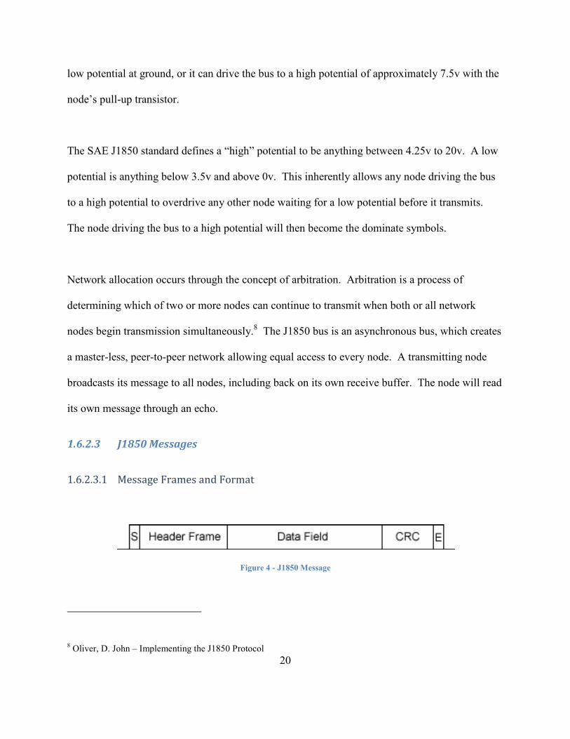
1.6.2.3 J1850 Messages
1.6.2.3.1 Message Frames and Format
Figure 4 - J1850 Message
8 Oliver, D. John – Implementing the J1850 Protocol

21
Messages are limited to a 12-byte frame (PWM) or a 101-bit frame (VPW), which includes a
Cyclical Redundancy Check Byte (CRC) and an In-Frame Response (IFR) byte. This frame is
comprised of an Active Start-of-Frame symbol, followed by a series of 8-bit messages, and
closed by a Passive End-of-Frame symbol. In the 12-byte frame, data is transferred sending the
Most Significant Byte (MSB) first.
The message starts with a Start of Frame (SOF), denoted by the ‘S’ in Figure 4, symbol. This
SOF is crucial for carrier sense and arbitration purposes. The SOF is defined as being a high
potential on the J1850 bus for a period of 200µs. Once the SOF symbol is transmitted on the
data bus, bit symbols are transferred. Any number of bytes between one and eleven can be
transferred.
Message Header Byte-Frame
The header byte contains information about what a receiving node should expect in the
proceeding message frame. Once the SOF symbol is sent on the J1850 bus, the header frame is
the next set of 8-bits transferred. The Header Frame is pictured in Figure 5.
Figure 5 - J1850 Message Header Frame
The first three bits are considered to be the Message Priority value. The priority value ranges
from 000 (highest priority) to 111 (lowest priority). This gives 8 values for the priority of a
particular message.
22
The next bit to get transferred is called the “Header Type.” This bit defines the message coming
as either being a three-byte message or a one-byte message. A value of “0” in this Header Type
value forecasts a three-byte header, while a value of “1” forecasts a one-byte header.
Following the Header Type bit is the In-Frame-Response (IFR) requirement flag. This bit
defines whether an In-Frame Response is requested or not. This bit is also called the K-bit. If
this bit is set to “zero,” then an IFR is requested. With a “one” bit flagged, no IFR is requested.
Next, the source sends to the bus an Addressing Mode bit, also called the “Y” bit. The Y bit
conveys to the receiver that the message is using one of two types of addressing associated with
the J1850 protocol. One is a functional type of addressing, and the other is called physical type.
If this “Y” bit is set to zero, then functional addressing is used. Conversely, if the Y-bit is set to
“one,” then physical addressing is used. Functional addressing has a higher priority than the
physical addressing has, providing that all preceding bits are the exact same.
1.6.2.3.2 Functional Addressing
Functional Addressing is a scheme that labels messages based on their operation code or the
message’s content. This type of messaging is important for networks where a target receiver
node does not have a publically known physical address, but its function to the entire network is
known.(Powers, 1992) This and other nodes can be addressed by utilizing a function code, to
which the node that has the specific function will answer.

23
1.6.2.3.3 Physical Addressing
Physical Addressing is an addressing scheme that labels messages based upon the physical
address location of their source and / or their destination. While physical addressing is
independent of the geographic location, connector pins, and / or wire identification assignments
of the node, the addressing occurs for nodes which have a specific hardware identifier. The node
with the specific physical address will answer the request(Valentine, 1998).
1.6.2.4 J1850 Bit Definitions
Since all communication which happens on the J1850 Bus is through binary bits, and the active
and passive voltage levels have little to do with the bits’ value, the time division multiplier must
be defined such that the message can be deciphered. There are four types of bits which can be
sent on the data bus. The four types are Active 1, Active 0, Passive 1, and Passive 0. These bits
are depicted further in a non-scale Figure 6.
Figure 6 - SAE J1850 Bit Symbol Timings
24
1.6.2.5 Emulating J1850 VPW Bits
1.6.2.5.1 Bit Emulation Using Software
Sending and receiving data bits using the J1850 VPW protocol involves setting a signal line to
high and low for variable amounts of time. This proves to be difficult in that we need an exact
time value at ever edge on the signal, since the amount of time that the line stays at a particular
state is what denotes the value of the bit.
Further, if software is used to generate the waveform, the processes needed to run the other code
of the system will be tied up, and the system will only be able to perform one function at a time.
This would cause problems with timing, as well as halt other operations needed to translate,
transmit, and receive data. It is for these reasons that software cannot be trusted to perform the
exact calculations of each rising and falling edge. With this requirement in mind, it is still
helpful to implement a software waveform generation so that the concept can be proven and a
waveform resembling the VPW protocol can be created.
Doing so was not difficult. We know the speed of the processor, and how many clock ticks
happen with each instruction. We were able to implement a signal that generated 0xAA
(0b01010101) on the line at all times. The waveform was a bit off, but this is to be expected
with the weight associated with the instructions being used to change the line’s state.

25
1.6.2.5.2 Bit Emulation using Hardware
One of the most important features of the ATmega168 is its timers’ ability to enter WGM, or
Wave Generation Mode. With WGM, we were able to implement a Pulse-Width-Modulation
(PWM) waveform that had a constant period. Having a hardware-implemented timer gives the
engineer freedoms that software does not. Most importantly, the engineer is not tied to any other
processes when dealing with a hardware timer. No matter what the microcontroller is doing,
when a hardware interrupt occurs, the process stops, and a hardware interrupt routine is
performed.
PWM by definition has a constant period, with a variable amount of its period that stays at either
a high or a low state. Although the period is constant, this variable high or low time, or ‘the duty
cycle,’ could be changed by setting a particular variable counter that was constantly compared to
the counter’s value through hardware means. This particular variable ranges from 0 to 256. If
one wants a 0% duty cycle, he or she would set this counter to 0. If one wanted a 75% duty
cycle, this value would be set to 191. Figure 7 shows two PWM waveforms, one with 90% duty
cycle, and one with 50% duty cycle.

The amount of time that the signal stays at high or low is controllable by a variable, thus
allowing an engineer the ability to have 100% duty cycles and 0% duty cycles together in
sequences. Understanding this basic concept was instrumental in setting up
using a PWM signal.
More specifically, one could set up a timer that interrupts every 16 microseconds. This timer
would generate a signal with 100% duty cycle for 4 interrupts, allowing us to generate a “high”
signal for 64 microseconds, then switch to a 0% duty cycle therea
protocol as an “Active 0” signal! So, by allowing a PWM to run for a particular amount of time
26
Figure 7 - PWM Waveform Examples
The amount of time that the signal stays at high or low is controllable by a variable, thus
allowing an engineer the ability to have 100% duty cycles and 0% duty cycles together in
sequences. Understanding this basic concept was instrumental in setting up the VPW signal
More specifically, one could set up a timer that interrupts every 16 microseconds. This timer
would generate a signal with 100% duty cycle for 4 interrupts, allowing us to generate a “high”
signal for 64 microseconds, then switch to a 0% duty cycle thereafter, defined by the J1850 VPW
protocol as an “Active 0” signal! So, by allowing a PWM to run for a particular amount of time
The amount of time that the signal stays at high or low is controllable by a variable, thus
allowing an engineer the ability to have 100% duty cycles and 0% duty cycles together in
the VPW signal
More specifically, one could set up a timer that interrupts every 16 microseconds. This timer
would generate a signal with 100% duty cycle for 4 interrupts, allowing us to generate a “high”
fter, defined by the J1850 VPW
protocol as an “Active 0” signal! So, by allowing a PWM to run for a particular amount of time
with a particular duty cycle, we have generated a waveform that conforms to an external
communications protocol.
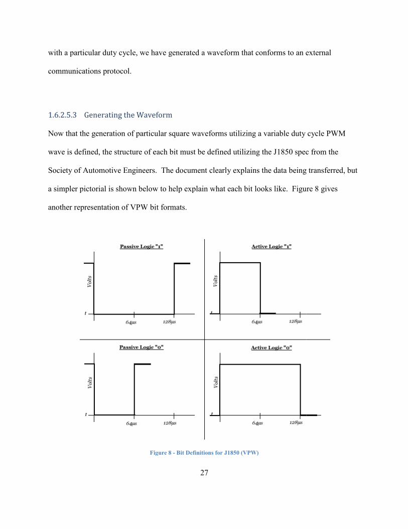
1.6.2.5.3 Generating the Waveform
Now that the generation of particular square waveforms utilizing a variable duty cycle PWM
wave is defined, the structure of each bit must be defined utilizing the J1850 spec from the
Society of Automotive Engineers. The document clearly explains
a simpler pictorial is shown below to help explain what each bit looks like.
another representation of VPW bit formats
Figure
27
with a particular duty cycle, we have generated a waveform that conforms to an external
Waveform
Now that the generation of particular square waveforms utilizing a variable duty cycle PWM
wave is defined, the structure of each bit must be defined utilizing the J1850 spec from the
Society of Automotive Engineers. The document clearly explains the data being transferred, but
a simpler pictorial is shown below to help explain what each bit looks like. Figure
another representation of VPW bit formats.
Figure 8 - Bit Definitions for J1850 (VPW)
with a particular duty cycle, we have generated a waveform that conforms to an external
Now that the generation of particular square waveforms utilizing a variable duty cycle PWM
wave is defined, the structure of each bit must be defined utilizing the J1850 spec from the
the data being transferred, but
Figure 8 gives
28
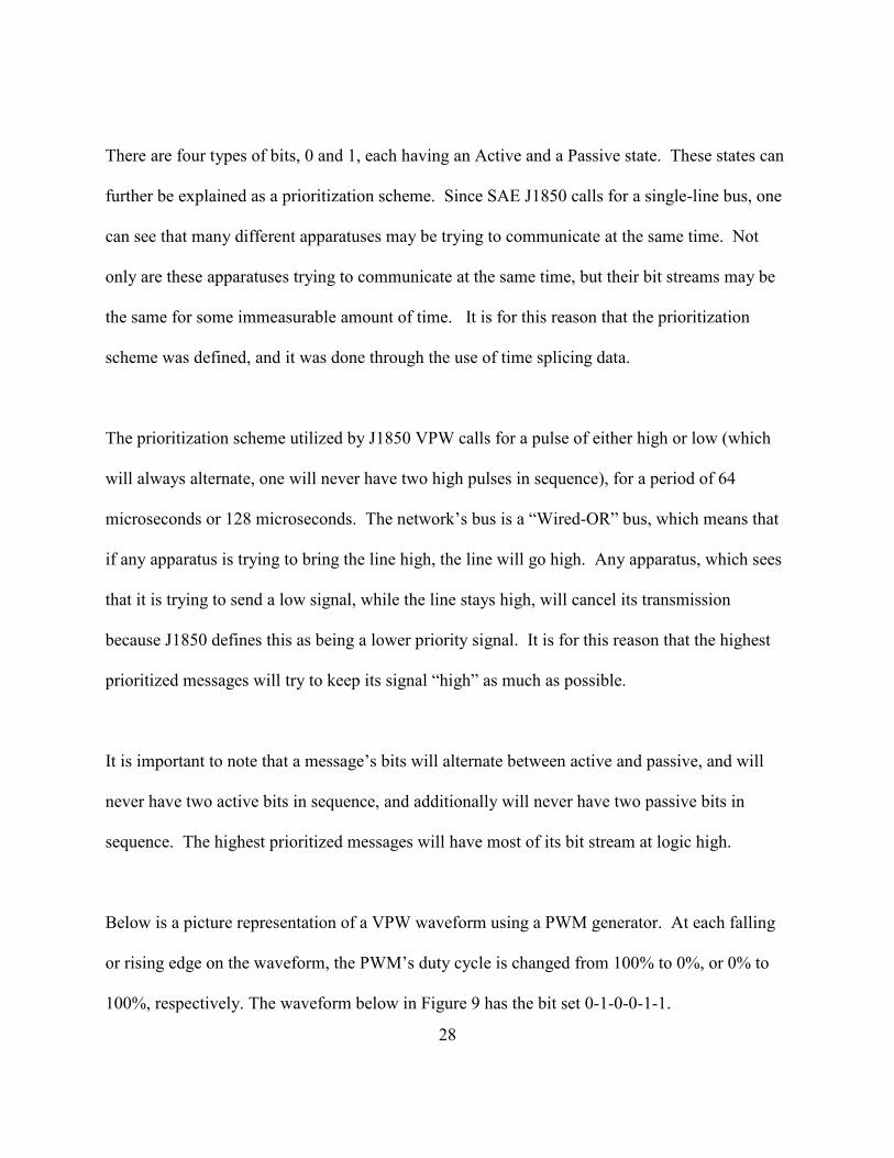
There are four types of bits, 0 and 1, each having an Active and a Passive state. These states can
further be explained as a prioritization scheme. Since SAE J1850 calls for a single-line bus, one
can see that many different apparatuses may be trying to communicate at the same time. Not
only are these apparatuses trying to communicate at the same time, but their bit streams may be
the same for some immeasurable amount of time. It is for this reason that the prioritization
scheme was defined, and it was done through the use of time splicing data.
The prioritization scheme utilized by J1850 VPW calls for a pulse of either high or low (which
will always alternate, one will never have two high pulses in sequence), for a period of 64
microseconds or 128 microseconds. The network’s bus is a “Wired-OR” bus, which means that
if any apparatus is trying to bring the line high, the line will go high. Any apparatus, which sees
that it is trying to send a low signal, while the line stays high, will cancel its transmission
because J1850 defines this as being a lower priority signal. It is for this reason that the highest
prioritized messages will try to keep its signal “high” as much as possible.
It is important to note that a message’s bits will alternate between active and passive, and will
never have two active bits in sequence, and additionally will never have two passive bits in
sequence. The highest prioritized messages will have most of its bit stream at logic high.
Below is a picture representation of a VPW waveform using a PWM generator. At each falling
or rising edge on the waveform, the PWM’s duty cycle is changed from 100% to 0%, or 0% to
100%, respectively. The waveform below in Figure 9 has the bit set 0-1-0-0-1-1.

Figure
The above waveforms in Figure 9
period of either 64 microseconds or 128 microseconds translate into active and passive bits as
defined in Figure 8. With these tools of generating a VPW waveform, one can now begin to
29
Figure 9 - J1850 VPW Waveform using PWM Signals
9 depict true bit transfers of J1850 VPW. Square waves of
period of either 64 microseconds or 128 microseconds translate into active and passive bits as
. With these tools of generating a VPW waveform, one can now begin to
depict true bit transfers of J1850 VPW. Square waves of
period of either 64 microseconds or 128 microseconds translate into active and passive bits as
. With these tools of generating a VPW waveform, one can now begin to
30
structure bit streams that resemble OBD-II messages, which can be given to scan tools, vehicle
OBD-II ports, or alternatively any other communications method utilizing a variable pulse width.
1.6.2.5.4 J1850 Bus Error Checking
J1850 defines a CRC, or Cyclical Redundancy Check byte, that provides a sanity check for the
communications device. Coupled with the other 11 bytes of data in the message frame, it
completes the message.
The entire message is considered a “word.” This word is then divided by a particular polynomial
set by the manufacturer implementing the J1850 protocol. Once the word is divided by this
polynomial, the “1’s complement” is taken of the result, and appended to the end of the message,
again completing the message.
The word message is received by a node in the bus, and checked against this polynomial. The
node will divide the message by the polynomial, take the 1’s complement, and compares this
complement to the CRC byte. If they match, then it can be assured that this message is complete
and no data transmission error has occurred.
1.6.3 Controller Area Networks
1.6.3.1 CAN Background9
Robert Bosch GmbH, the world’s largest automotive components supplier, pursued a method to
better communication within a vehicle’s electrical and mechanical system. Bosch chose the Intel
Corporation, the world’s largest semiconductor company, to join on this venture. The objective

31
for the electrical and mechanical system project was to make automobiles more efficient in
respect to fuel consumption, emissions, weight, and reliability. Together in 1983, these
companies delivered the Controller Area Network, CAN.
Controller Area Networks is a protocol that uses content addressed messaging in a broadcast
manor. Every node on the network receives every message transmitted. Acknowledgement
immediately is sent and the message is then discarded or kept to be processed by each node. By
using CSMA/CD (Carrier Sense Multiple Access/Collision Detection) each node can gain access
to the bus equally, and by using dominant and recessive identification, the process runs smoothly
with the appropriate information arriving first. Fault Confinement is used by CAN to address
faulty nodes and if need be, automatically turning them off to guarantee the network’s
availability.
CAN Protocol patents are owned by Robert Bosch GmbH, and a CAN Protocol License is
required as described below in the information from Bosch.com:
“Additionally to the CA� IP modules offered by Bosch, a CA� Protocol License is required.
The CA� Protocol License is also required for self-developed CA� modules, or for CA�
modules purchased from another vendor. Bosch is licensing the CA� protocol as follows:
1. CA� Protocol License for ASIC-manufacturers and FPGA mass programming
Performance of Bosch:
• Delivery of the CA� Protocol Specification together with comprehensive
explanations
• Delivery of a functional C Reference CA� Model

32
• Granting the right to use the CA� know-how and the CA� patents for the
manufacture of ASICs or the programming of FPGAs with CA� and their
worldwide sale
2. CA� Protocol License for FPGA Programming
Performance of Bosch:
• Granting the right to use the CA� patents for the programming of FPGAs
with CA� and their worldwide sale”
1.6.3.2 Message / Frame Types
CAN uses a message based protocol often referred to as ‘content-addressed.’ Content-addressed
implies that each message has the destination within. A priority and the data to be transferred is
embedded into the message and broadcasted to every node on the network. It is up to the nodes
to acknowledge that the message was received properly and to discard or process the message.
Messages can be sent to an abundance of nodes and processed or processed by a single node
according to who is destined to receive it. Messages are referred to as ‘Frames’ and there are four
types of frames in the CAN protocol. The frame types are defined as the Data Frame, Remote
Frame, Error Frame, and Overload Frame. Each type is explained below in Table 2.
CAN Message/Frame Types
Data Frame Always used when information
transmits.
Remote Frame
Same properties as a Data Frame with
an additional bit to signify it is a
Remote Transmit Request (RTR bit)
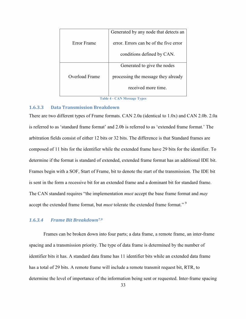
33
Error Frame
Generated by any node that detects an
error. Errors can be of the five error
conditions defined by CAN.
Overload Frame
Generated to give the nodes
processing the message they already
received more time.
Table 4 - CA1 Message Types
1.6.3.3 Data Transmission Breakdown
There are two different types of Frame formats. CAN 2.0a (identical to 1.0x) and CAN 2.0b. 2.0a
is referred to as ‘standard frame format’ and 2.0b is referred to as ‘extended frame format.’ The
arbitration fields consist of either 12 bits or 32 bits. The difference is that Standard frames are
composed of 11 bits for the identifier while the extended frame have 29 bits for the identifier. To
determine if the format is standard of extended, extended frame format has an additional IDE bit.
Frames begin with a SOF, Start of Frame, bit to denote the start of the transmission. The IDE bit
is sent in the form a recessive bit for an extended frame and a dominant bit for standard frame.
The CAN standard requires “the implementation must accept the base frame format and may
accept the extended frame format, but must tolerate the extended frame format.” 9
1.6.3.4 Frame Bit Breakdown7,9
Frames can be broken down into four parts; a data frame, a remote frame, an inter-frame
spacing and a transmission priority. The type of data frame is determined by the number of
identifier bits it has. A standard data frame has 11 identifier bits while an extended data frame
has a total of 29 bits. A remote frame will include a remote transmit request bit, RTR, to
determine the level of importance of the information being sent or requested. Inter-frame spacing

34
is used by both data frames and remote frames to separate them from the previous frame. These
bit fields are called inter-frames and most often consist of 96 bits. The space is allotted to
provide intermission between frames for other transmissions to commence as well as the
opportunity to suspend transmission. The last part is the transmission priority of each frame.
Dominant bits are designated with logical 0 and recessive bits a logical 1. Messages include
dominant and or recessive bits to identify the importance and resulting in a priority based
transmission method. The method is known as automatic arbitration free transmission. The
message with the highest priority will be processed while all other messages wait to be resent
and processed.
Figure 10 - Standard Frame Breakdown, Texas Instruments, Introduction to CA�
1ame Bits Definition
SOF 1 The start of frame bit notates the start of a message. It is also used to synchronize the nodes on a bus when they have been idle.
11 Bit Identifier
11 The 11 bit identifier includes the priority of the message. A higher priority message, as previously stated, has a lower binary value.
RTR 1 The remote transmission request bit is dominant in the event that the information is required from another node.
IDE 1 Identifier Extension bit is a dominant bit that will identify the information to be of standard frame.
R0 1 Reserved bit currently not used.
DLC 4 The Data length code containing the number of bytes of data being transmitted.
Data <64 the data field
CRC 16 The cyclic redundancy check, 15 bits and a delimiter. The CRC contains the number of bits

35
being transmitted of the preceding application data for error detection.
ACK 2 The acknowledgement bit, plus a delimiter, that every node overwrites after successfully receiving an accurate message. The recessive bit is overwritten with a dominant bit if an error free message has been sent. In the event that a node detects an error, the bit is left as recessive and the message is discarded. As a result the sending node will retransmit the original message.
EOF 7 The End of frame bit field that notates the end of the frame.
IFS 7 The inter-frame space. The inter-frame space is designed to give a controller the necessary time to move a correctly received frame to its destination in the buffer
Table 5 - Standard Frame Bit Definitons
Figure 11 - Extended Frame Breakdown, Texas Instruments, Introduction to CA�
1ame Bits Definition
SOF 1 The start of Frame bit notates the start of a message. It is also used to synchronize the nodes on a bus when they have been idle.
SRR 1 The substitute remote request bit, used to place hold where the RTR bit is usually located in the standard message.
IDE 1 Identifier Extension bit is a recessive bit that will identify the information to be of extended frame.
18 Bit Identifier
18 The 18 bit identifier includes the priority of the message. A higher priority message, as previously stated, has a lower binary value.
RTR 1 Remote transmission request bit is dominant in the event that the information is required from another node.
R1 1 Reserved bit currently not used
R0 1 Reserved bit currently not used

36
DLC 4 The Data length code containing the number of bytes of data being transmitted.
Data <64 the data field
CRC 16 The cyclic redundancy check, 15 bits and a delimiter. The CRC contains the number of bits being transmitted of the preceding application data for error detection.
ACK 2 The acknowledgement bit, plus a delimiter, that every node overwrites after successfully receiving an accurate message. The recessive bit is overwritten with a dominant bit if an error free message has been sent. In the event that a node detects an error, the bit is left as recessive and the message is discarded. As a result the sending node will retransmit the original message.
EOF 7 End of frame bit field that notates the end of the frame
IFS 7 The inter-frame space. The inter-frame space is designed to give a controller the necessary time to move a correctly received frame to its destination in the buffer.
Table 6 - Extended Frame Bit definitions
1.6.3.5 Non-Return-to-Zero
NRZ, Non-Return-to-Zero line code is a transmission method used by CAN where logic ‘1’s are
represented by a high voltage and a logic ‘0’ are represented by low voltage. There is no rest
condition, with CAN, but bit stuffing is used. 9
1.6.3.6 Bit Stuffing
CAN is asynchronous, meaning that it is does not require a global clock signal but uses the
recovering clock information from the data stream. Here, CAN uses Bit Stuffing. For CAN, Bit
Stuffing is the process in which an opposing polarity bit will be put into the data stream if five
bits of the same polarity are sent. Used only for synchronization, the bit is disregarded and not
used as data. 5

37
1.6.3.7 Error Detection7,8,9
1.6.3.7.1 CRC Error
The CRC, cyclic redundancy check, is a 15 bit value calculated by the transmitting node,
transmitted in the CRC field. The cyclic redundancy check is a way to ensure that all the nodes
on the network received the correct message. If the CRC calculated by each node on the network
does not the CRC values broadcasted, an Error Frame will is generated and the message will be
resent.
1.6.3.7.2 Acknowledge Error
For at least one node to correctly receive a message, an Acknowledge Slot must contain a
dominant bit. If the bit is a recessive bit, then the message transmitted was not received by any
node correctly. As a result an Error Frame is generated and the message will be resent.
1.6.3.7.3 Form Error
In the case that an End of Frame, Inter-frame Space, Acknowledge Delimiter or CRC Delimiter
contains a dominant bit, a Form Error is generated. As a result, the message will be resent.
1.6.3.7.4 Bit Error
A Bit Error will occur in the event that a transmitter sends a dominant bit and a recessive bit is
identified. A Bit Error will also take place when a recessive bit is sent and a dominant bit is
detected. As a result of the detection, an Error Frame is generated and the message is resent.
1.6.3.7.5 Stuff Error
A Stuff Error occurs in the condition that Bit Stuffing is not properly executed and six bits with
the same polarity are transmitted and or detected. An Error Frame is sent and the message is
resent.

38
1.6.3.8 Fault Confinement9
According to the severity of an error, CAN nodes are capable of determining fault condition and
transition to error states. This process is called Fault Confinement and is implemented to
guarantee bandwidth for critical system information.
1.6.3.9 Three CAN Error States1,5,6,7,8,9
In the event that an Error Frame of Error flag is created, the transmission of the message that
resulted in the error is terminated. The message will be resent when it has the network
availability. Below are the three types or error states:
1.6.3.9.1 Error-Active
If a node’s Transmit Error Counter and Receiver Error Counter are below 128, it is Error Active.
While a node is Error Active, communication with the bus can still take place and an error flag
will be send. An error flag is comprised of six dominant bits violating the Bit Stuffing rule. As a
result, every node sends an Error flag. During this process, the Error ‘Echo’ Flag is sent from all
the other nodes in addition to the Error Flag, can send up to twelve consecutive dominant bits.
1.6.3.9.2 Error-Passive
When the Transmit Error Counter (TEC) and Receiver Error Counter (REC) exceed 127 a node
becomes Error Passive. Opposite of Error-Active, when a node is Error-Passive, six recessive
bits are transmitted as the Error Flag. In the event that the Error-Passive node’s message is the
only message being sent, acknowledgement of the Bit Stuffing rule violation will be made from
the receiving nodes. There is no effect on the bus unless the Error Passive node is the only
transmitter.

39
Table 7 - SO 11898, Bredband.net, CA1 Information
1.6.3.9.3 Bus –Off
If the Transmit Error Counter is greater than 255, the node will immediately go into the Bus-Off
state. Nodes are not able to send, receive or acknowledge messages in this state. Error frames can
also not be sent. The justification of the Bus-Off state is to keep the network available for
transmission of other important information.
1.6.3.10 Speed and Voltages 5
CAN is defined by ISO 11898 or ISO 114519. Data transfer rates range from a maximum of
1Mbps to a minimum of 10kbps. Communication lines used on the OBDII connector are Pin 6
as a high, Pin14 as a low. In addition CAN uses two ground types, Pin 4 as the Chassis Ground,
and Pin 5 as the Signal Ground. The two communication lines operate in a differential mode
where the voltages carried are inverted to decrease noise interference. Pin 16 is the voltage of the
battery. Below are the standards for the voltage levels for both the ISO 11898 and ISO 11519;
Signal recessive state dominant state unit
min nominal max min nominal max
CAN-High 1.6 1.75 1.9 3.85 4.0 5.0 Volt
CAN-Low 3.1 3.25 3.4 0 1.0 1.15 Volt
ISO 11519, Breband.net, CA� Information
Table 8 - ISO 11519, Breband.net, CA1 Information
Signal recessive state
dominant state
unit
min nominal max min nominal max
CAN-High 2.0 2.5 3.0 2.75 3.5 4.5 Volt
CAN-Low 2.0 2.5 3.0 0.5 1.5 2.25 Volt
40
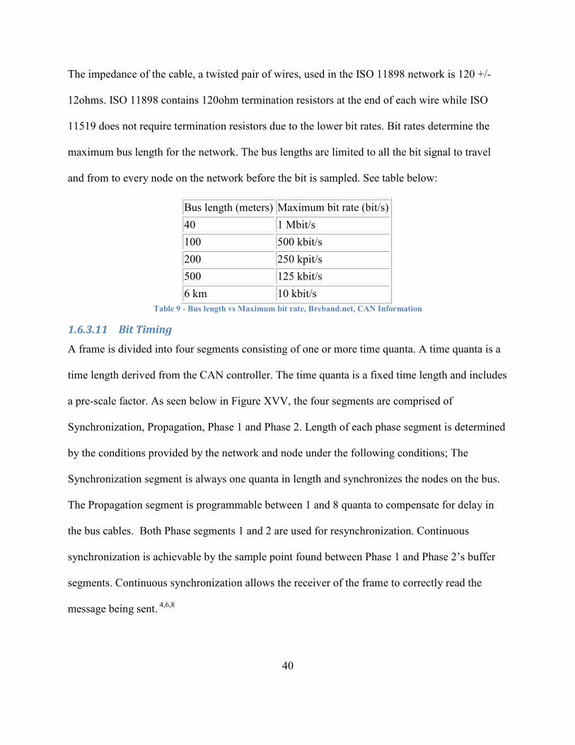
The impedance of the cable, a twisted pair of wires, used in the ISO 11898 network is 120 +/-
12ohms. ISO 11898 contains 120ohm termination resistors at the end of each wire while ISO
11519 does not require termination resistors due to the lower bit rates. Bit rates determine the
maximum bus length for the network. The bus lengths are limited to all the bit signal to travel
and from to every node on the network before the bit is sampled. See table below:
Bus length (meters) Maximum bit rate (bit/s)
40 1 Mbit/s
100 500 kbit/s
200 250 kpit/s
500 125 kbit/s
6 km 10 kbit/s
Table 9 - Bus length vs Maximum bit rate, Breband.net, CA1 Information
1.6.3.11 Bit Timing
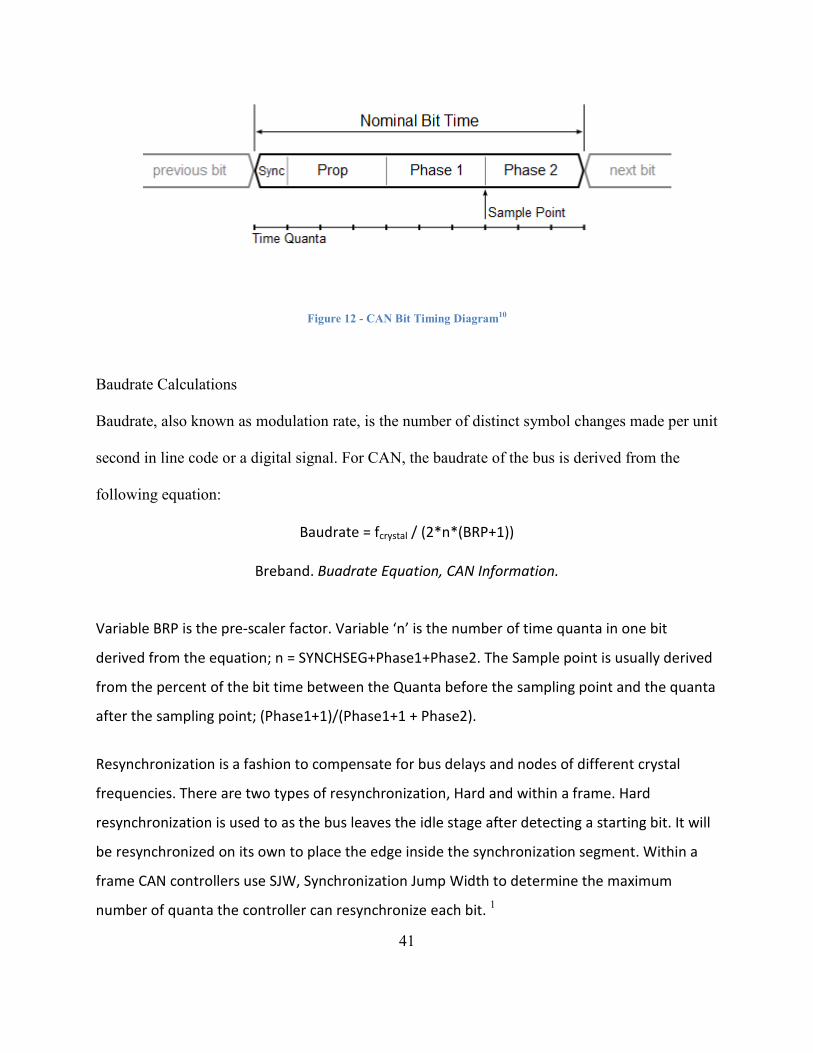
A frame is divided into four segments consisting of one or more time quanta. A time quanta is a
time length derived from the CAN controller. The time quanta is a fixed time length and includes
a pre-scale factor. As seen below in Figure XVV, the four segments are comprised of
Synchronization, Propagation, Phase 1 and Phase 2. Length of each phase segment is determined
by the conditions provided by the network and node under the following conditions; The
Synchronization segment is always one quanta in length and synchronizes the nodes on the bus.
The Propagation segment is programmable between 1 and 8 quanta to compensate for delay in
the bus cables. Both Phase segments 1 and 2 are used for resynchronization. Continuous
synchronization is achievable by the sample point found between Phase 1 and Phase 2’s buffer
segments. Continuous synchronization allows the receiver of the frame to correctly read the
message being sent. 4,6,8
41
Figure 12 - CA1 Bit Timing Diagram10
Baudrate Calculations
Baudrate, also known as modulation rate, is the number of distinct symbol changes made per unit
second in line code or a digital signal. For CAN, the baudrate of the bus is derived from the
following equation:
Baudrate = fcrystal / (2*n*(BRP+1))
Breband. Buadrate Equation, CAN Information.
Variable BRP is the pre-scaler factor. Variable ‘n’ is the number of time quanta in one bit
derived from the equation; n = SYNCHSEG+Phase1+Phase2. The Sample point is usually derived
from the percent of the bit time between the Quanta before the sampling point and the quanta
after the sampling point; (Phase1+1)/(Phase1+1 + Phase2).
Resynchronization is a fashion to compensate for bus delays and nodes of different crystal
frequencies. There are two types of resynchronization, Hard and within a frame. Hard
resynchronization is used to as the bus leaves the idle stage after detecting a starting bit. It will
be resynchronized on its own to place the edge inside the synchronization segment. Within a
frame CAN controllers use SJW, Synchronization Jump Width to determine the maximum
number of quanta the controller can resynchronize each bit. 1
42
1.6.3.12 Network Structure
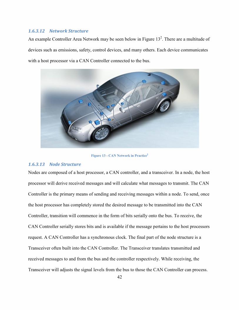
An example Controller Area Network may be seen below in Figure 132. There are a multitude of
devices such as emissions, safety, control devices, and many others. Each device communicates
with a host processor via a CAN Controller connected to the bus.
Figure 13 - CA1 1etwork in Practice2
1.6.3.13 Node Structure
Nodes are composed of a host processor, a CAN controller, and a transceiver. In a node, the host
processor will derive received messages and will calculate what messages to transmit. The CAN
Controller is the primary means of sending and receiving messages within a node. To send, once
the host processor has completely stored the desired message to be transmitted into the CAN
Controller, transition will commence in the form of bits serially onto the bus. To receive, the
CAN Controller serially stores bits and is available if the message pertains to the host processors
request. A CAN Controller has a synchronous clock. The final part of the node structure is a
Transceiver often built into the CAN Controller. The Transceiver translates transmitted and
received messages to and from the bus and the controller respectively. While receiving, the
Transceiver will adjusts the signal levels from the bus to those the CAN Controller can process.
43
While sending, the Transceiver takes converts the signal provided by the CAN Controller to that
of which the bus requires. In addition to the Transceiver’s receiving and sending capabilities, it
also provides the CAN Controller with a buffer protective circuitry layer. 5
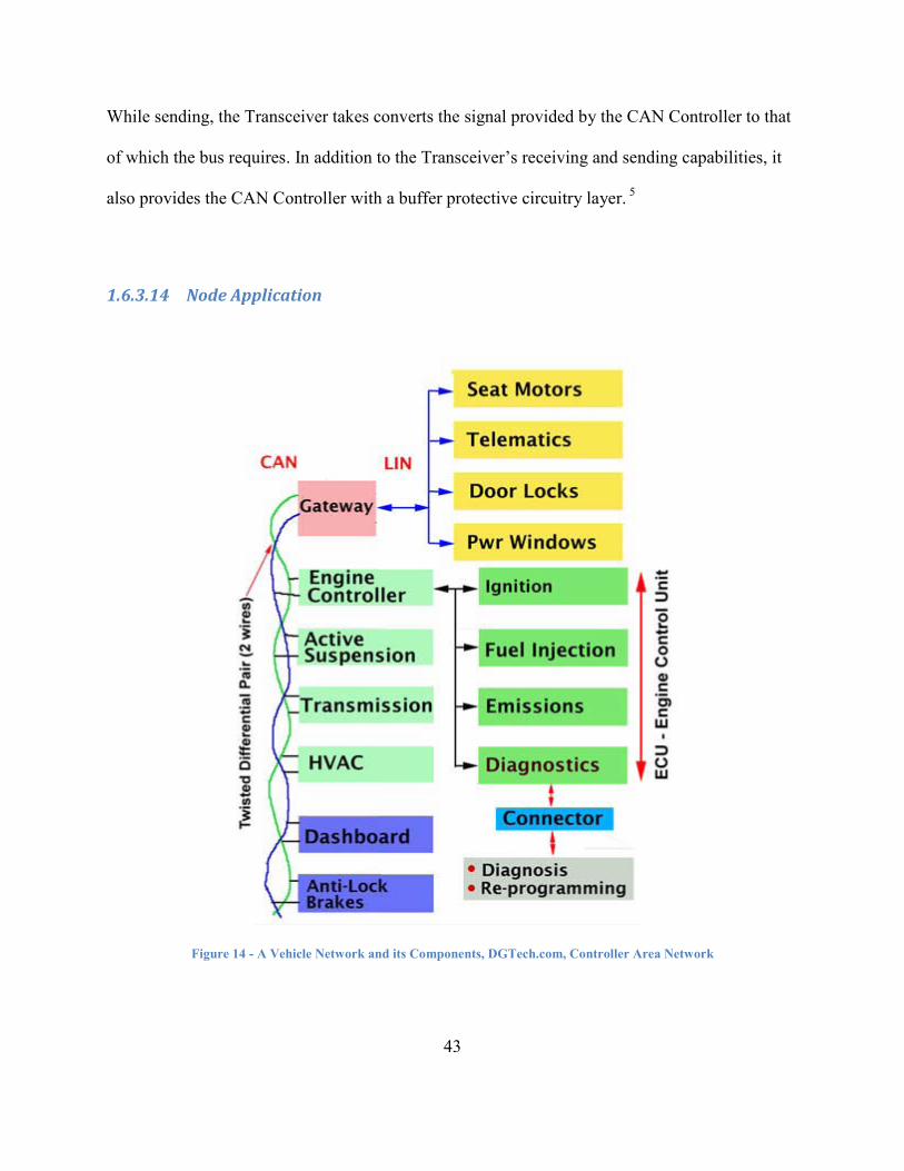
1.6.3.14 Node Application
Figure 14 - A Vehicle 1etwork and its Components, DGTech.com, Controller Area 1etwork

44
Figure 14 connects a Controller Area Network bus with a Local Interconnect Network bus by a
gateway located within one of the Electronic Control Modules of the vehicle most often in the
Engine Control Unit. The Engine Control Unit is where the vital engine control functions are
located and is a clearinghouse for the vehicle’s diagnostics in this case, OBDII. 3
1.6.4 Implementation of OBD-II Protocols
Once an engineer understands the protocols described above, he or she can interface with any
communications device which uses these protocols.
To shorten the time to market, this project team decided to use a third part interface chip to
communicate with vehicles. Taking care of this communication allows this project team to focus
on the translation of the data coming from the vehicle to that which is transmitted over the
wireless connection. One needs to create a new layered architecture to accomplish the feat of
translation. The Mobile Wireless Unit will be responsible for reading any and all messages from
the vehicle’s OBD-II port and translating these messages to RS232 signals, thus eliminating the
ambiguity of understanding which protocol is being used on the Vehicle. This would ensure that
any communication on the RS232 line will never be protocol specific, and will always be in the
context of speaking to the ELM chip on the Mobile Wireless Unit. This is an important concept
for the rest of the project. It is important that only significant information be transmitted to the
RS232. This information cannot be tied to a particular protocol, and should ignore any
idiosyncrasies among the different protocols.

45
This means of transporting information is very similar to the problems network engineers first
faced when creating the internet. It was decided very early that there would be particular
“layers” to a network, and that each layer would have particular functions that no other layer
would ever worry about understanding. This separates the abilities of the layers, and thus allows
each layer to be very specialized in its nature.
The proposed architecture for this project is similar to a network layer structure as it has two
layers, a physical layer and a application layer. The physical layer would handle all direct
communications with the outside interfaces. This includes the OBD-II port on the vehicle, and a
possible scan tool made for interfacing with the vehicles OBD-II port. Once any communication
came from outside communications, its signal would then be translated into bits, and handed off
to the next layer, the transport layer. The transport layer would send the message’s bits through
a communications means which would allow another point to translate those bits into a signal
that could be read by an outside interface. A picture representation can be seen below in Figure
15.
Figure 15 - Layer Protocol in use for this system
46
As one can see, the separation of functions in this respect helps isolate steps needed in order to
interface with different communications means. Particularly when dealing with four different
protocols, it can be easy to become overwhelmed with the amount of data being sent. Separating
functions into clear layers has allowed us to methodically step through the transmission of this
data.
Data coming from the vehicle is translated into RS232 codes using a circuit defined by the
Mobile Wireless Unit’s project specification. This RS232 signal is then transmitted wirelessly
through the XBee ZigBee protocol, to be captured by the Arduino programming environment.
The Arduino then reads the bits, understands what they mean, and translates these bit sets in a
way described below to be sent using the VPW protocol. Doing these small steps sequentially
allows the transmission of data to be methodical and very precise on the bit level.
2 Project Definition
2.1 Understanding Possible Target Markets
Interviewing mechanics and employees of local consumer auto parts stores proved to be valuable
in identifying a problem that there is inefficiency in the way OBD-II codes are transmitted from

47
the car to the professional. This inefficiency can be eliminated with a product which removed
the most important part of the OBD-II scan tool from the untrained user’s custody.
2.1.1 AutoZone
One of the possible customers that were identified was AutoZone. AutoZone is a consumer
automotive parts store that sells a multitude of products to end consumers. Founded in 1979,
AutoZone is a multi-country, public company that offers consumer auto parts. Consumers can
visit a store and have their car scanned for OBDII codes, which helps in the diagnosis of what
the customer needs to buy.
The inherent problem with allowing customers to “borrow” a scan tool is that the scan tool is not
always returned. Further, the scan tool can be mishandled by untrained customers and come
back in a worse condition. Over time, the scan tool will be used to the point that the unit will
break from the wear and tear of untrained users. Therein lays a problem where the use of the
scan tool by untrained users causes a loss in the assets of a particular company, in this case,
AutoZone.
The product which this MQP team intends to create will solve the problem of asset loss, and help
keep the most important parts of a scan tool in the hands of the professionals. The base unit,
which accepts, reformats, and transmits through either a USB cord or to the regular scan tool.
The unit sent with the customer, however, is a unit which transmits the codes directly only and
does no calculation or reporting.
48
Having a setup this way would help AutoZone in that they will no longer have to send a
professional staff member with consumers to plug the unit into their cars. Giving the unit to the
consumer and instructing them on where to place the plug is the only work that needs to happen.
The unit instructs the user when the signals are complete, and can remove the unit. Once these
instructions are given, the user unplugs the unit, and walks back into the AutoZone shop. The
attendant has already seen the codes and has the ability to print out product listings and
instructions for the customer.
This increases the store’s revenue and frees up man hours for the staff, which allows the
AutoZone to do better staffing, and better business. AutoZone would benefit both financially
and operationally from the use of this product.
2.1.2 Emissions Testing Garages
A second possible customer is identified as the Automotive Inspection Bays throughout the
United States. With over 230 million vehicles on the road in the US, Automotive Bays have
continuously run inspection tests on vehicles since 1996. Comprised within the inspection testing
are three major sub-tests; Visual, Safety and Emissions inspection. Safety and Visual
inspections are serious parts of the overall test, but the focus of our product is on the emissions.
A certified technician will connect a male OBDII connector from the state regulated machine,
such as The SPX Corporation Emission Analyzer, directly to the vehicle’s female OBDII
connector. The vehicle’s female OBDII connector is connected to the vehicle’s internal

49
computer. The internal computer holds the information on how the vehicle’s engine and
emissions controls have been operating. The technical will then download the data from the
vehicle into his or hers computer. If the data received will be inform the technician if the vehicle
passes the emissions test.
According to the technicians that were interviewed for market research on this product,
inspections may take anywhere between 15 and 30 minutes per vehicle. Often times customers
are lost due to waiting time on the availability of the testing equipment. As a result, each
technician explained how vehicle efficiency could greatly be increased with the use of wireless
connections, and the possibility of having information readily available to transfer from the
vehicles for emissions testing.
A simple connection with the wireless connector alone would allow the location of the vehicle to
not be mandated. Moving vehicles around, being restricted to a minimum distance from the
machine takes up time. Bottom line, time is money. The faster the test can correctly be
completed the more money per hour the Inspection Bay will make.
Advanced to the next stage, the process can become an assembly line with the introduction of the
multi-vehicle wireless connections. In the event that there are only a few days left in the month,
every month, Automotive Inspection Bays receive a major positive spike in the number of
vehicles being tested. This is partly due to the Citation issued by the state for a moving vehicle
infraction. An outdated inspection sticker is a $50 fine with a direct result on personal driver’s
insurance. On like examples, multiple vehicles will be in line to be tested and the assembly line

50
may be introduced. In example, as one technician focuses on visual inspection and inserting an
identifiable wireless connection in each vehicle another technician can quickly go through and
run them individually through the computer. As a result, production is increased and profit
increases.
2.2 Customer Requirements
The following customer requirements were generated from the interviews with the target market.
Mechanics from local automotive shops, attendants at inspection bays, and employees at
consumer automotive part stores were interviewed in this subset of the target market for this
product. The list is as follows.
• Durable & Sturdy
• Informative
• Parking lot distance wireless capability
• Easy to use
• Comparable price to wired units
• Fit current architecture
2.3 Product Specifications
The following product specifications are derived from the appropriate customer requirements.
Each Product Specification is identified in direct result to satisfy a Customer Requirement.
1 The system passes all data sent from OBD-II port connected to the Mobile Wireless
Unit to the Base Station Unit, connected to a scan tool.
2 The system must be able to function without any problems under normal working
conditions. Normal working conditions include exposure to dust, dirt, and a
frequency of usage which ranges between 5 to 30 times per day

51
3 The Base Station Unit must inform the user that it is connected with a Mobile
Wireless Unit correctly or incorrectly. As a result, the user must know if he or she is
able to send and receive data through the Base Station Unit to communicate with the
OBD-II data port on the automobile outside.
4 The unit functions at a range of up to 100 feet
5 The system is simple enough to require no user interaction to ensure proper function.
The Mobile Wireless Unit only needs to be connected correctly to the OBD-II port on
an automobile, and the Base Station Unit to an OBD-II scan tool.
6 Unit is compatible with protocols J1850 VPW, J1850 PWM, ISO 9141-2, and
Automotive CAN.
3 Product Design
3.1 System Flow
The theoretical unit designed and created in this document is comprised of multiple parts. There
is a mobile, wireless unit which is taken to the vehicle, and there is a base station which is not
designed to move very far or travel very often.
3.1.1 Mobile Wireless Unit
The Mobile Wireless Unit (MWU) is designed to be transported by hand from the base station’s
area and brought directly to the OBD-II code source, usually a consumer automobile. The user
plugs the unit into the female adapter of the automobile’s OBD-II port.

52
3.1.1.1 Mobile Wireless Unit Block Diagram
The Mobile Wireless Unit will have the components laid out in such a way that it can interface
with all types of OBD-II protocols. The block diagram is shown in Figure 16.
Figure 16 - Mobile Wireless Unit Block Diagram
The block diagram will further be broken into its subcomponents. There needs to be a wireless
communications interface which communicates with another mesh network node. This wireless
communications interface would further interface with the microprocessor in the MWU. As
more is understood about the signals produced by and through OBD-II standards, a filter will be
created to interface with the specific protocol used in the vehicle in question.
With all of the above information being true, a final block diagram is created to display the
actual setup for the Mobile Wireless Unit.
53
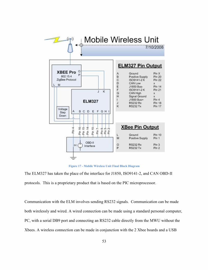
Figure 17 - Mobile Wireless Unit Final Block Diagram
The ELM327 has taken the place of the interface for J1850, ISO9141-2, and CAN OBD-II
protocols. This is a proprietary product that is based on the PIC microprocessor.
Communication with the ELM involves sending RS232 signals. Communication can be made
both wirelessly and wired. A wired connection can be made using a standard personal computer,
PC, with a serial DB9 port and connecting an RS232 cable directly from the MWU without the
Xbees. A wireless connection can be made in conjunction with the 2 Xbee boards and a USB

54
cable to a computer with USB ports. The platform used to send and receive data is a standard
HyperTerminal that comes in most PCs. With this, the baud rate can be set to the needed 9600
baud and the appropriate communication port selected. With the connection made between the
PC and the MWU, the male J1962 connector may be plugged into the vehicles female J1962 port
and the first message ‘ELM327 v1.3.’ will be displayed in the HyperTerminal. On the second
line will be the ELM327 prompt character ‘>.’ The MWU is ready to receive characters from the
HyperTerminal and begin use. These character commands can be found in the Elm Electronics
ELM327 appendices attached to this paper.1
The block diagram is simplified into a series of step up transistors, step-down transistors,
resistors, voltage dividers, and the ELM. With these in place, the Mobile Wireless Unit is an
eloquent solution to a complex problem. This project team is now able to interface with the
vehicle’s OBD-II port, regardless of protocol, using RS232 signals.
This is truly a breakthrough in the project, as it allows a communications standard to interface
with another communications standard. While the chip may be a bit more expensive than that of
an internally developed solution, it allows this team to get to the market faster, and once the
product is in the market, the team will search for second generation alternatives to
implementation techniques, including but not limited to, the designing of a new system to
exclude the ELM327 chip.

55
3.1.1.2 Mobile Wireless Unit Use
The user puts the automobile in a state which will cause the automobile to deliver OBD-II codes.
This method is completed differently for each protocol and automobile, and is not standard. The
Mobile Wireless Unit runs off of the voltage which is supplied by the automobile, on Pin 16 of
the OBD-II port. The voltage coming out of the OBD-II port is the voltage of the automobile’s
battery, so it is stepped down by a voltage divider. Once the Mobile Wireless Unit is powered,
an indicator LED turns illuminates in a solid state to notify the user that the unit is on and is
ready to connect to the base.
The Mobile Wireless Unit always assumes that if it is supplied with power, it is to be
transmitting information to the Base Station Unit. Thus, upon being powered, no user interaction
is needed to create the wireless link between the Mobile Wireless Unit and the Base Station. All
codes sent to the unit during this connection phase are lost.
Once a connection is made between the Mobile Wireless Unit and the Base Station, the indicator
light, which once signified power by staying in a solid, illuminated state, will now blink at a
steady rate to notify the user that there is successful communication happening with the Base
Station.
The connection created will allow the constant, instant transfer of codes gathered by the Mobile
Wireless Unit to the Base Station Unit. The Base Station Unit has two different ways of
analyzing and distributing the received data, explained in the next section of this document.

56
The Mobile Wireless Unit knows when the codes being sent are repeating or are complete, and
illuminates a second, different colored LED to notify the user that transmission is complete and a
complete code set has been transferred.
3.1.2 Base Station Unit
The Base Station Unit, or BSU, sends and receives information to and with the Mobile Wireless
Unit. The BSU is always in a state waiting for a connection request. Once the Base Station Unit
detects a request to connect from a Mobile Wireless Unit, a handshaking process occurs between
the units.
Upon a successful connection handshaking process, the Mobile Wireless Unit transmits data to
and from the Base Station Unit. The Base Station Unit has the functionality to pass data
immediately through to an existing OBD-II Scan Tool, and has the hardware required to connect
through USB to any peripheral device which can connect to USB.
The BSU should have the ability to connect multiple Mobile Wireless Units simultaneously, so
that the limitation of a one-to-one ratio of connectors to scanners is eliminated. A block diagram
of the Base Station Unit is shown below in Figure 18.

57
Figure 18 - Base Station Unit Block Diagram
With this identified, the members of this project team can begin work on creating this part of the
project, which involves two interfaces.
3.1.2.1 Pass-Through Functionality
Initially the BSU is set up to only pass through data which is being sent through the wireless
connection. The data is accepted from the Mobile Wireless Unit, the BSU then sets the voltage
of each corresponding OBD-II pin to match the data being sent from the Mobile Wireless Unit.
This is the functionality which is implemented in the completion of this project.
58
3.2.1.1 USB Connectivity
The BSU should have the ability to collect data from multiple Mobile Wireless Units
simultaneously and transfer this information in real time to a computer connected through USB.
This functionality opens the door to an unbelievable amount of extended features. Services
could be created which would enrich the use of this product solution.
Possible additional services include monthly updates with new automobile support, computer
program upgrades and support, mass data storage, and other online services which may be
identified at a later date.
3.2 System Block Diagram
The Mobile Wireless Unit transmits information wirelessly to the Base Station Unit. The Base
Station Unit also has transmission capability with the Mobile Wireless Unit. As these units
transmit data between themselves, data must also be sent and received from peripheral devices to
make this product useful to a consumer. The BSU has a female OBD-II adapter as part of its
architecture, and allows the end user to interface with the automobile’s OBD-II port from a
sheltered, remote location. The OBD-II female port on the BSU is virtually the same port as that
to which the Mobile Wireless Unit is plugged. Figure 19 illustrates a high level block diagram of
the final functioning system.
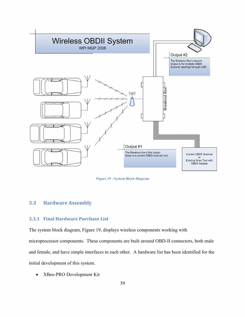
59
Figure 19 - System Block Diagram
3.3 Hardware Assembly
3.3.1 Final Hardware Purchase List
The system block diagram, Figure 19, displays wireless components working with
microprocessor components. These components are built around OBD-II connectors, both male
and female, and have simple interfaces to each other. A hardware list has been identified for the
initial development of this system.
• XBee-PRO Development Kit

60
• Arduino Development Kit
• Rabbit Semiconductor Development Kit
• USB Development Board
The above hardware sets were available through online resources directly from manufacturers.
3.3.1.1 XBee-PRO Development Kit
For the purposes of this project, the team has chosen to use RS232 to communicate among
interfaces involved with the Mobile Wireless Unit and the Base Station Unit, and further a
computer receiver or a commercial scan-tool. It became increasingly important to choose a
medium of wireless communication that understood and replicated RS232 signals. The research
completed led the team to the use of the XBee-PRO.
The XBee-PRO is a wireless communication platform created by Digi. The platform allows the
communication of RS232 signals without the in-depth knowledge required to program difficult
to use other wireless protocols. The XBee-PRO utilizes the ZigBee protocol, which is a mesh-
network protocol created for close-proximity nodes in a network. An example of proposed
ZigBee use includes home automation, where one node can communicate with another.
For example, while at work, a person can send a command through the internet to have his or her
stove, which had been refrigerating a turkey, to change temperatures to defrost, or even begin to
cook the turkey, so that travel time can be used effectively, and dinner for the family would be
ready at a more convenient time.
61
Another example of ZigBee’s proposed use is that of traffic engineering. Each car would be
equipped with this relatively inexpensive product, and a mesh network would be created.
Information about the car’s speed, and data about a driver’s tendency to change lanes and
acceleration data can all be collected for future reference of developing better traffic flow
control.
As a relatively new technology, this MQP team believed that it was the best option for the
purpose of wirelessly communicating OBD-II data between the MWU and the BSU. This puts
the MQP team right in line with emerging technologies, and allows this project to function using
products at a discount. We were able to obtain a few chips at relatively low-cost, and were able
to prove the concept of wirelessly communicating utilizing this protocol at a reasonable price.
Thankfully, this technology ended up being a great solution and we are happy with the decision
to move forward with the XBee PRO.

62
3.3.1.2 Arduino Microprocessor Development Kit
The Arduino Development Board includes the Atmega168 microprocessor on its board. There is
a large sized following for people on the internet who use this architecture for all types of
applications. The team felt that this board would best suit the needs of this project, and would
interface nicely with the ZigBee-PRO wireless circuits.
Figure 20 shows the Pin Mapping for the Arduino board. The black, inner text is used to identify
the function for which the microprocessor uses, and the outer red text is used to show for what
function the Arduino uses the pin.

63
Figure 20 - Arduino Pin Configuration9
Understanding this pin configuration became increasingly important as the project continued, as
the chip would often have to be removed from the Arduino environment to ensure that the digital
state of the pin was correct, and that the predictive nature of microprocessors were correct.
Lastly, the PWM pins used in the software implementation were simply digital pins which were
changed with an internal function. This project had to rewrite the code to ensure that the PWM
signals were being generated utilizing hardware interfaces instead of software digitalWrite
commands.
3.3.2 Identification of Interfaces
3.3.2.1 Mobile Wireless Unit Interfaces
The ZigBee-PRO development kit will interface with the Arduino microprocessor through a
breakout board purchased through a company called SparkFun.com. The breakout shield is
pictured below in Figure 21.
9 Arduino – Atmega168Hardware: http://www.arduino.cc/en/Hacking/Atmega168Hardware
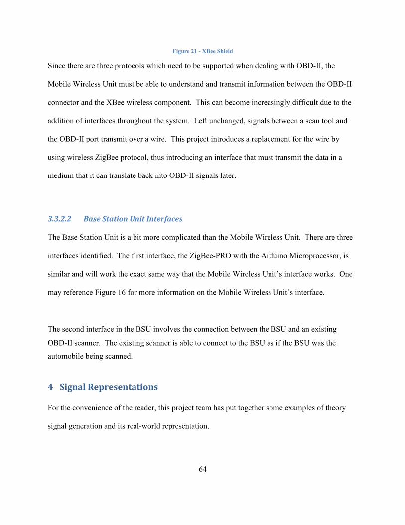
64
Figure 21 - XBee Shield
Since there are three protocols which need to be supported when dealing with OBD-II, the
Mobile Wireless Unit must be able to understand and transmit information between the OBD-II
connector and the XBee wireless component. This can become increasingly difficult due to the
addition of interfaces throughout the system. Left unchanged, signals between a scan tool and
the OBD-II port transmit over a wire. This project introduces a replacement for the wire by
using wireless ZigBee protocol, thus introducing an interface that must transmit the data in a
medium that it can translate back into OBD-II signals later.
3.3.2.2 Base Station Unit Interfaces
The Base Station Unit is a bit more complicated than the Mobile Wireless Unit. There are three
interfaces identified. The first interface, the ZigBee-PRO with the Arduino Microprocessor, is
similar and will work the exact same way that the Mobile Wireless Unit’s interface works. One
may reference Figure 16 for more information on the Mobile Wireless Unit’s interface.
The second interface in the BSU involves the connection between the BSU and an existing
OBD-II scanner. The existing scanner is able to connect to the BSU as if the BSU was the
automobile being scanned.
4 Signal Representations
For the convenience of the reader, this project team has put together some examples of theory
signal generation and its real-world representation.
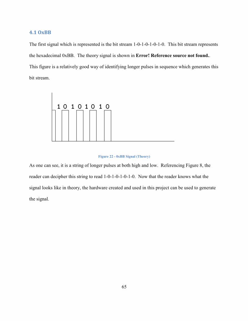
65
4.1 OxBB
The first signal which is represented is the bit stream 1-0-1-0-1-0-1-0. This bit stream represents
the hexadecimal 0xBB. The theory signal is shown in Error! Reference source not found..
This figure is a relatively good way of identifying longer pulses in sequence which generates this
bit stream.
Figure 22 - 0xBB Signal (Theory)
As one can see, it is a string of longer pulses at both high and low. Referencing Figure 8, the
reader can decipher this string to read 1-0-1-0-1-0-1-0. Now that the reader knows what the
signal looks like in theory, the hardware created and used in this project can be used to generate
the signal.

66
Figure 23 - 0xBB Signal (Practice)
0xBB has been created using the hardware in this project. A Two channel digital real time
oscilloscope has been used to show the signal in its truest form. For convenience, the black box
above the signal in Figure 23 helps the reader decipher where the bits are 0, and where they are
1.
4.2 Ox55
The second example theory vs. practice signals generated using J1850 VPW is 0x55, which has
the bit stream 0-1-0-1-0-1-0-1. One may assume that this bit stream is the same over time as 1-
0-1-0-1-0-1-0, but that is not the case. Since there is an additional consideration of the Bus’ last
state, the active signals versus the passive signals change their dynamic and the reader will see
that there is now a different signal. Figure 24 shows a representation for this signal in theory.
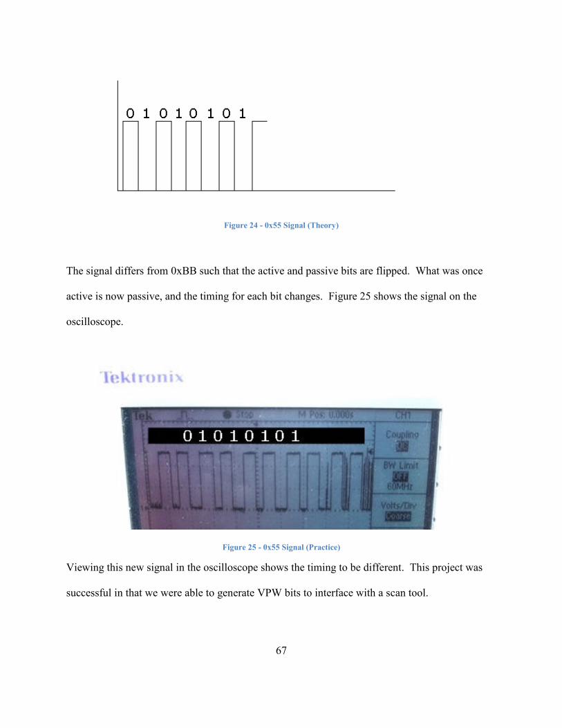
67
Figure 24 - 0x55 Signal (Theory)
The signal differs from 0xBB such that the active and passive bits are flipped. What was once
active is now passive, and the timing for each bit changes. Figure 25 shows the signal on the
oscilloscope.
Figure 25 - 0x55 Signal (Practice)
Viewing this new signal in the oscilloscope shows the timing to be different. This project was
successful in that we were able to generate VPW bits to interface with a scan tool.
68
5 Proof of Concept
There has been a successful transmission of vehicle OBD-II codes through the XBee-PRO, a to a
computer program as of October 22, 2008. John Keenan utilized a circuit built from the
ELM327 datasheet to interface with a setup that Sean Mahoney had created utilizing the XBee-
PRO architecture.
The Arduino programming environment can successfully generate PWM bits and VPW bits as
defined by the J1850 standard, showing this project to be a further success than originally
planned.
6 Recommendations
Two of the biggest challenges faced by this group included time constraints and man hour
constraints. There were goals that were set forth in the beginning which were unable to be
accomplished, but may have been completed with more time or with additional resources.
5.1 Multiple Mobile Wireless Units
Originally, this project had set forth to create a system which allowed multiple Mobile Wireless
Units to communicate with a singular Base Station Unit. This goal was unfortunately not
achieved due to the time constraints, but work was done to carefully allow the completion of this
goal if and when the next project team decides to move forward with this functionality.

69
The next project team which decides to implement this feature should carefully study the ZigBee
Mesh protocol to find out addressing techniques and further understand how protocol addressing
is handled.
5.2 Scan Tool Implementation
One recommendation that this project would like to make to all future projects is that hardware
truly is the best way to solve repeated, time-critical solutions. Implementing the signal
generation for VPW in software was somewhat of a waste of time, it was inaccurate, was subject
to hardware interrupts, and caused a lot of valuable time resources to be used. The knowledge of
what the signal was supposed to look like was available, and it may have been helpful to have
proof of concept, but it truly ended up wasting time, and the implementation for both VPW and
PWM should have happened on the hardware from the beginning.
Implementing signal generation utilizing hardware interrupts is truly the way to implement
communications protocols. The hardware understands when an interrupt is to occur, and it
allows implemented software to perform functions when the signal on a line is at its correct state.
While the hardware was waiting for another interrupt, the next bit value could be loaded into a
temporary placeholder for the interrupt routine to read. Since this move takes a very little
amount of clock cycles, it can be assured that this execution will not be missed through hardware
interrupts.
70
6 Conclusions
Due to the intense work done to interface with a vehicle’s diagnostic’s port, this team was able to
achieve multiple goals set forth in the initial planning stages of this project. The team was able
to successfully interface with a vehicle’s OBD-II port, and send those codes wirelessly to a
computer. The team was able to then further achieve the goal of sending codes back through the
wireless connection to have those codes delivered to the vehicle’s OBD-II port. The team was
also able to receive live codes from the vehicle as those codes change and update as the vehicle
is being driven.
The team was able to successfully interface with a vehicle’s OBD-II port. This OBD-II port is
based on standards that are proprietary and standard across the world. This project has the
ability to interface with a vehicle through J1850 VPW, J1850 PWM, CAN, ISO 9141, KWM,
and variations of these protocols, as well. The ability to do this was paramount in the creation of
this project, and identified the first major milestone in the project.
The second great accomplishment of this project was that of the wireless connection. This team
further proved that RS232 signals could wirelessly be transmitted in a way that could be
predicted to a Base Station Unit, utilizing the ZigBee protocol for a point-to-point network
(rather than its initial use, a mesh-network).
The third accomplishment builds on this accomplishment, by sending RS232 signals through the
wireless connection to interface with the OBD-II port on the vehicle. This is truly a great
71
accomplishment as it shows that, as shown in Figure 15, a layered network protocol works
perfectly for this implementation. This project was able to successfully remove protocols from
the equation of sending pure bit-by-bit data through a communication medium introduced by this
project. Sending commands through the wireless connection for interaction with the OBD-II
protocol port solidified this project’s success.
All things considered, the base, fundamental accomplishment involves the emulation of bits
utilizing the VPW, PWM J1850 protocols. This was a major milestone in the project because it
concretely showed proof of concept for generation of these protocols’ signals. With this
knowledge, we were able to create an interface that not only communicates with scan tool, but it
also essentially reacts the same way the vehicle’s OBD-II port does to requests from a scan tool.
While there was a bit of adversity faced between the team members of this project, the end result
required much work and a strong commitment from the two partners. There is much that could
have resulted in a stronger project completion; however, we believe that we learned a great deal
not only about automotive standard protocols, but interfaces in general. Future projects
involving the ground-up creation of electronics will run more smoothly due to the guidance
provided by Professor Bitar. We would like to officially thank him for all of his help and
guidance throughout the project.
72
Bibliography
Powers, Chuck. 1992. AN1212. [Online] 1992. [Cited: June 23, 2008.] http://www.diy-
efi.org/gmecm/ecm_info/obd2/AN1212.REV0.PDF.
Valentine, Richard. 1998. Motor Control Electronic Handbook. Motor Control Electronic
Handbook. s.l. : McGraw Hill, 1998.
Perquin. 2001. OBD-II [Online] 2001. [Cited: July 25, 2008.] http://prj.perquin.com/obdii/
Beyer, Ronald. 2005. OBD-II Specifications [Cited: April 19, 2008.]
http://obdproject.com/OBD2Info/Specs/
Mictronics Forum. 2005. AVR J1850 VPW Interface [Online.]
http://www.mictronics.de/smf/index.php?topic=155.15
Stern, Trampas. 2005 AVR J1850 Interface Code [Online]
http://avrobdii.googlecode.com/svn/trunk/code/J1850.c
California, University of. 2006. Serial Communications [Online]
http://esd.cs.ucr.edu/labs/serial/serial.html
Diagnostics, OBD. 2005. OBDII Message Structure [Online]
http://www.obddiagnostics.com/obdinfo/msg_struct.html
Technologies, Werner. 2002. OBD2 Standards/Terms. [Online.]
http://www.obd2crazy.com/techstd.html
Davis, Leroy. 1998. Glossary of Electronics and Engineering OBD Terms. [Online]
http://www.interfacebus.com/Glossary-of-Terms_OBD-interface.html
Davis, Leroy. 1998. SAE J1850 Description, Electrical Interface Bus [Online.]
http://www.interfacebus.com/Automotive_SAE_J1850_Bus.html

73
Davis, Leroy. 1998. CA� Bus Interface Description, CA� Bus Pinout, and Signal �ames,
Controller Area �etwork [Online.]
http://www.interfacebus.com/Design_Connector_CAN.html
Oliver, D John. Implementing the J1850 VPW protocol. [Online.]
http://developer.intel.com/design/intarch/papers/j1850_wp.pdf
Breband. CA� Information, Baudrate Equation. http://hem.breband.net
Robert Bosch GmbH. http://bosch.com
DGTech. A Vehicle �etwork and its Components, Controller Area �etwork. http://DGTech.com
Etschberger, Konrad. Controller Area �etwork. 2001
Intel. Introduction to the Controller Area �etwork (CA�) Protocol. 1995
Kvaser Advanced CAN Solutions. The CA� Protocol Tour. http:// kvaser.com/can/protocol
Lawrenz, Wolfhard. From Theory to Practical Applications: CA�. 1997.
1ational Instruments. Controller Area �etwork (CA�). http://ni.com/can/
Robert Bosch GmbH, CA� Specifications. 1991
Texas Instruments, Introduction to CA�. 1997.
Wikimedia.org, Image:CA� Bit Timing2.svg. CAN Bit Timing Diagram
Related Documents


