Instructor: Alexander Stoytchev http://www.ece.iastate.edu/~alexs/classes/ CprE 281: Digital Logic

Welcome message from author
This document is posted to help you gain knowledge. Please leave a comment to let me know what you think about it! Share it to your friends and learn new things together.
Transcript

Instructor: Alexander Stoytchev
http://www.ece.iastate.edu/~alexs/classes/
CprE 281: Digital Logic

Registers and Counters
CprE 281: Digital Logic Iowa State University, Ames, IA Copyright © Alexander Stoytchev

Administrative Stuff • The second midterm is this Friday.
• Homework 8 is due today.
• Homework 9 is out. It is due on Mon Nov 7.
• No HW due next Monday

Administrative Stuff • Midterm Exam #2
• When: Friday October 28 @ 4pm.
• Where: This classroom
• What: Chapters 1, 2, 3, 4 and 5.1-5.8
• The exam will be open book and open notes (you can bring up to 3 pages of handwritten notes).

Registers

Register (Definition)
An n-bit structure consisting of flip-flops

Parallel-Access Register

1-Bit Parallel-Access Register
D Q
Q
Clock
In Out
Load
0 1

1-Bit Parallel-Access Register
D Q
Q
Clock
In Out
Load
0 1
The 2-to-1 multiplexer is used to select whether to load a new value into the D flip-flop or to retain the old value. The output of this circuit is the Q output of the flip-flop.

1-Bit Parallel-Access Register
D Q
Q
Clock
In Out
Load
0 1
If Load = 0, then retain the old value. If Load = 1, then load the new value from In.

2-Bit Parallel-Access Register
D Q
Q
Clock
Load
0 1 D Q
Q
In_1
Out_0
0 1
Out_1
In_0
2-Bit Parallel-Access Register
D Q
Q
Clock
Load
0 1 D Q
Q
In_1
Out_0
0 1
Out_1
In_0
Parallel Input
Parallel Output
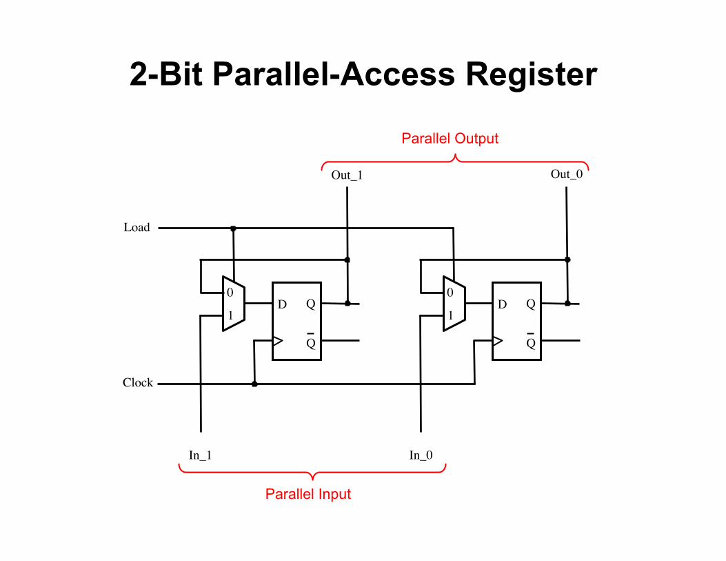
3-Bit Parallel-Access Register
D Q
Q
Clock
Load
0 1 D Q
Q
In_2
Out_1
0 1
Out_2
In_1
D Q
Q
Out_0
0 1
In_0
Notice that all flip-flops are on the same clock cycle.

3-Bit Parallel-Access Register
Parallel Input
Parallel Output
D Q
Q
Clock
Load
0 1 D Q
Q
In_2
Out_1
0 1
Out_2
In_1
D Q
Q
Out_0
0 1
In_0

4-Bit Parallel-Access Register
Clock
Load
D Q
Q
0 1
In_3
Out_3
D Q
Q
0 1
In_2
Out_2
D Q
Q
0 1
In_1
Out_1
D Q
Q
0 1
In_0
Out_0

4-Bit Parallel-Access Register
Parallel Input
Parallel Output
Clock
Load
D Q
Q
0 1
In_3
Out_3
D Q
Q
0 1
In_2
Out_2
D Q
Q
0 1
In_1
Out_1
D Q
Q
0 1
In_0
Out_0

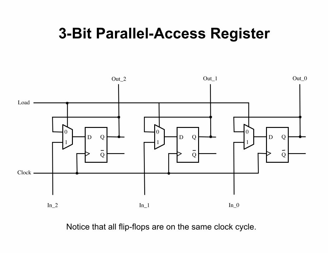
Shift Register

A simple shift register
D Q
Q Clock
D Q
Q
D Q
Q
D Q
Q
In Out Q 1 Q 2 Q 3 Q 4
[ Figure 5.17a from the textbook ]

A simple shift register
Positive-edge-triggered D Flip-Flop
D Q
Q Clock
D Q
Q
D Q
Q
D Q
Q
In Out Q 1 Q 2 Q 3 Q 4
A simple shift register
D Q Q
Master Slave D
Clock Q Q
D Q Q
Q m Q s
Clk Clk
D Q
Q Clock
D Q
Q
D Q
Q
D Q
Q
In Out Q 1 Q 2 Q 3 Q 4

A simple shift register
D Q Q
Master Slave D
Clock Q Q
D Q Q
Q m Q s
Clk Clk Gated D-Latch Gated D-Latch
D –Flip-Flop
D Q
Q Clock
D Q
Q
D Q
Q
D Q
Q
In Out Q 1 Q 2 Q 3 Q 4

A simple shift register
D Q
Q Clock
D Q
Q
D Q
Q
D Q
Q
In Out Q 1 Q 2 Q 3 Q 4

A simple shift register
D Q
Q Clock
D Q
Q
D Q
Q
D Q
Q
In Out Q 1 Q 2 Q 3 Q 4
D Q Q
Master Slave
Clk D Q
Q Clk D Q
Q
Master Slave
Clk D Q
Q Clk D Q
Q
Master Slave
Clk D Q
Q Clk D Q
Q
Master Slave
Clk D Q
Q Clk Clock In

A simple shift register
D Q
Q Clock
D Q
Q
D Q
Q
D Q
Q
In Out Q 1 Q 2 Q 3 Q 4
D Q Q
Master Slave
Clk D Q
Q Clk D Q
Q
Master Slave
Clk D Q
Q Clk D Q
Q
Master Slave
Clk D Q
Q Clk D Q
Q
Master Slave
Clk D Q
Q Clk Clock In

A simple shift register
D Q
Q Clock
D Q
Q
D Q
Q
D Q
Q
In Out Q 1 Q 2 Q 3 Q 4
D Q Q
Master Slave
Clk D Q
Q Clk D Q
Q
Master Slave
Clk D Q
Q Clk D Q
Q
Master Slave
Clk D Q
Q Clk D Q
Q
Master Slave
Clk D Q
Q Clk Clock In

A simple shift register
D Q
Q Clock
D Q
Q
D Q
Q
D Q
Q
In Out Q 1 Q 2 Q 3 Q 4
D Q Q
Master Slave
Clk D Q
Q Clk D Q
Q
Master Slave
Clk D Q
Q Clk D Q
Q
Master Slave
Clk D Q
Q Clk D Q
Q
Master Slave
Clk D Q
Q Clk Clock In

A simple shift register
D Q
Q Clock
D Q
Q
D Q
Q
D Q
Q
In Out Q 1 Q 2 Q 3 Q 4
D Q Q
Master Slave
Clk D Q
Q Clk D Q
Q
Master Slave
Clk D Q
Q Clk D Q
Q
Master Slave
Clk D Q
Q Clk D Q
Q
Master Slave
Clk D Q
Q Clk Clock In

A simple shift register
D Q Q
Master Slave
Clk D Q
Q Clk D Q
Q
Master Slave
Clk D Q
Q Clk D Q
Q
Master Slave
Clk D Q
Q Clk D Q
Q
Master Slave
Clk D Q
Q Clk Clock In

A simple shift register
D Q Q
Master Slave
Clk D Q
Q Clk D Q
Q
Master Slave
Clk D Q
Q Clk D Q
Q
Master Slave
Clk D Q
Q Clk D Q
Q
Master Slave
Clk D Q
Q Clk Clock In
Clock

A simple shift register
D Q Q
Master Slave
Clk D Q
Q Clk D Q
Q
Master Slave
Clk D Q
Q Clk D Q
Q
Master Slave
Clk D Q
Q Clk D Q
Q
Master Slave
Clk D Q
Q Clk Clock In
Clock

A simple shift register
D Q Q
Master Slave
Clk D Q
Q Clk D Q
Q
Master Slave
Clk D Q
Q Clk D Q
Q
Master Slave
Clk D Q
Q Clk D Q
Q
Master Slave
Clk D Q
Q Clk Clock In
Clock

A simple shift register
D Q Q
Master Slave
Clk D Q
Q Clk D Q
Q
Master Slave
Clk D Q
Q Clk D Q
Q
Master Slave
Clk D Q
Q Clk D Q
Q
Master Slave
Clk D Q
Q Clk Clock In
Clock

A simple shift register
[ Figure 5.17 from the textbook ]
D Q
Q Clock
D Q
Q
D Q
Q
D Q
Q
In Out
t 0 t 1 t 2 t 3 t 4 t 5 t 6 t 7
1 0 1 1 1 0 0 0
0 1 0 1 1 1 0 0
0 0 1 0 1 1 1 0
0 0 0 1 0 1 1 1
0 0 0 0 1 0 1 1
Q 1 Q 2 Q 3 Q 4 Out = In
(b) A sample sequence
(a) Circuit
Q 1 Q 2 Q 3 Q 4

Parallel-Access Shift Register
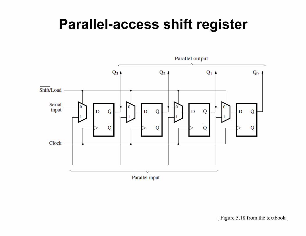
Parallel-access shift register
[ Figure 5.18 from the textbook ]

A shift register with parallel load and enable control inputs
[ Figure 5.59 from the textbook ]

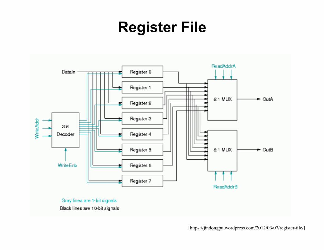
Register File
[https://jindongpu.wordpress.com/2012/03/07/register-file/]
Register File

[http://fourier.eng.hmc.edu/e85_old/lectures/digital_logic/node19.html]

[http://fourier.eng.hmc.edu/e85_old/lectures/digital_logic/node19.html]

[http://www.eecg.toronto.edu/~enright/teaching/ece243S/notes/l19-implemenation-single-cycle.html]

• Register file is a unit containing r registers § r can be 4, 8, 16, 32, etc.
• Each register has n bits § n can be 4, 8, 16, 32, etc. § n defines the data path width
• Output ports (DATA1 and DATA2) are used for reading the register file
§ Any register can be read from any of the ports § Each port needs a log2r bits to specify the read
address (RA1 and RA2) • Input port (LD_DATA) is used for writing
data to the register file § Write address is also specified by log2r bits (WA) § Writing is enabled by a 1-bit signal (WR)
Register File
Reg File
WA WR
RA2 RA1
LD_DATA
DATA1
DATA2
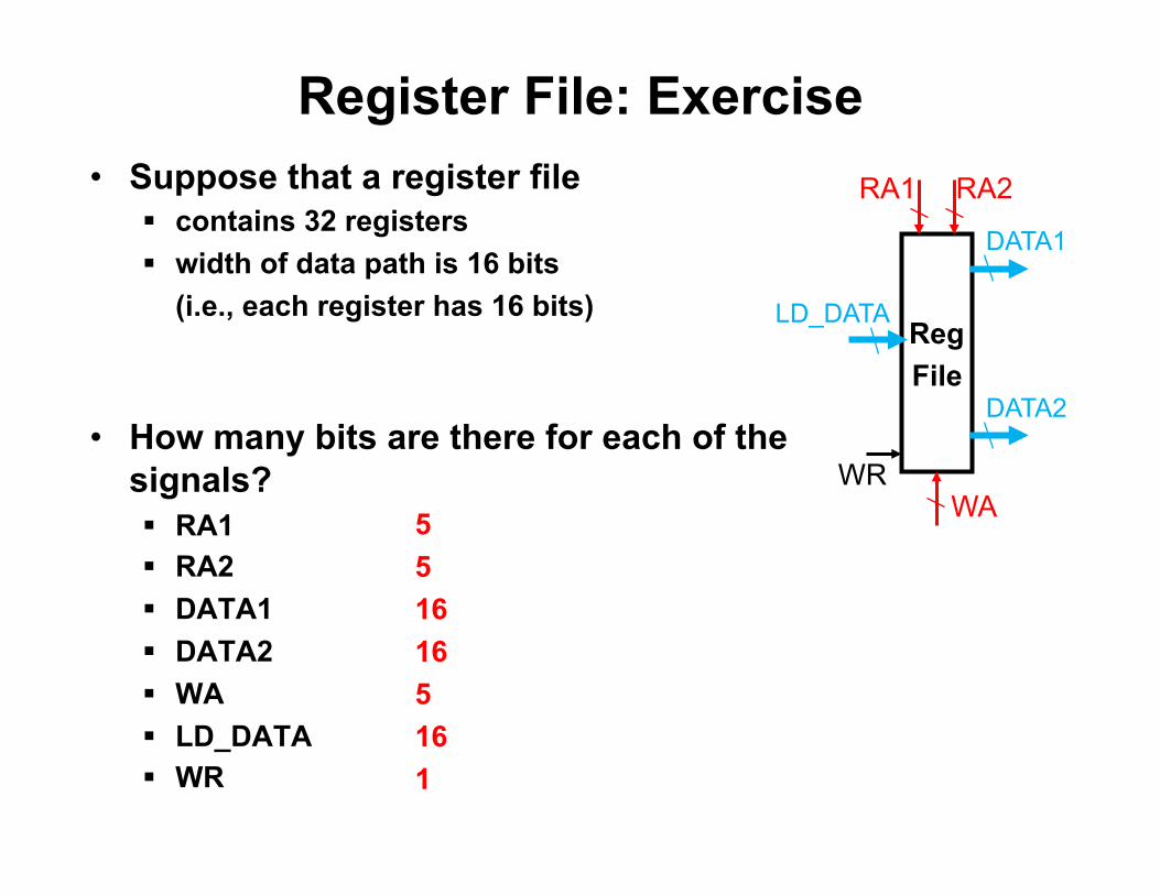
• Suppose that a register file § contains 32 registers § width of data path is 16 bits
(i.e., each register has 16 bits)
• How many bits are there for each of the signals? § RA1 § RA2 § DATA1 § DATA2 § WA § LD_DATA § WR
Register File: Exercise
Reg File
WA WR
RA2 RA1
LD_DATA
DATA1
DATA2
5 5 16 16 5 16 1

• We will design an eight-register file with 4-bit wide registers • A single 4-bit register and its abstraction are shown below
• We have to use eight such registers to make an eight register file
• How many bits are required to specify a register address?
Register file design
Q3 Q2 Q1 Q0
D3 D2 D1 D0
Clock
LD
Q3 Q2 Q1 Q0
D3 D2 D1 D0
Clk
LD
Q3 Q2 Q1 Q0
D3 D2 D1 D0
Clk
LD
Q3 Q2 Q1 Q0
D3 D2 D1 D0
Clk
LD
LD
Clock
Q0 Q1 Q2 Q3
D3 D2 D1 D0
D Q P
0 1
D Q P
0 1
D Q P
0 1
D Q P
0 1

• A 3-bit register address, RA, specifies which register is to be read
• For each output port, we need one 8-to-1 4-bit multiplier
7 6 5 4 3 2 1 0 8-to-1 4-bit multiplex RA1
DATA1
7 6 5 4 3 2 1 0 8-to-1 4-bit multiplex RA2
DATA2
Q3 Q2 Q1 Q0
D3 D2 D1 D0
Clk
LD0
Q3 Q2 Q1 Q0
D3 D2 D1 D0
Clk
LD1
Q3 Q2 Q1 Q0
D3 D2 D1 D0
Clk
LD7
Register Address
111 001 000
Reading Circuit

• To write to any register, we need the register's address (WA) and a write register signal (WR)
• A 3-bit write address is decoded if write register signal is present
• One of the eight registers gets a LD signal from the decoder
7 6 5 4 3 2 1 0 8-to-1 4-bit multiplex RA1
DATA1
7 6 5 4 3 2 1 0 8-to-1 4-bit multiplex RA2
DATA2
Q3 Q2 Q1 Q0
D3 D2 D1 D0
Clk
LD0
Q3 Q2 Q1 Q0
D3 D2 D1 D0
Clk
LD1
Q3 Q2 Q1 Q0
D3 D2 D1 D0
Clk
LD7
LD_DATA
WA
3 to 8 D e c o d e r WR
111 001 000 LD7
LD0 LD1 LD2
Adding write control to register file

Counters

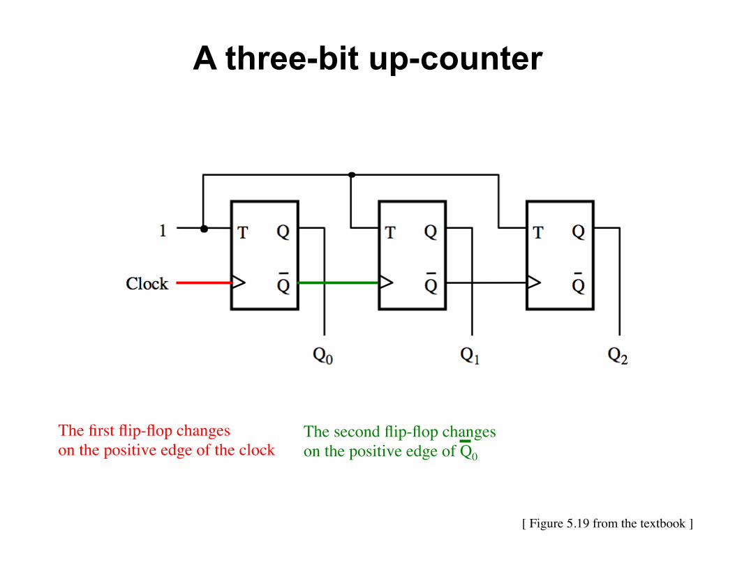
A three-bit up-counter
[ Figure 5.19 from the textbook ]

A three-bit up-counter
[ Figure 5.19 from the textbook ]
The first flip-flop changes on the positive edge of the clock
A three-bit up-counter
[ Figure 5.19 from the textbook ]
The first flip-flop changes on the positive edge of the clock
The second flip-flop changes on the positive edge of Q0

A three-bit up-counter
[ Figure 5.19 from the textbook ]
The first flip-flop changes on the positive edge of the clock
The second flip-flop changes on the positive edge of Q0
The third flip-flop changes on the positive edge of Q1

A three-bit up-counter
[ Figure 5.19 from the textbook ]
T Q
Q Clock
T Q
Q
T Q
Q
1
Q 0 Q 1 Q 2 (a) Circuit
Clock Q 0 Q 1 Q 2
Count 0 1 2 3 4 5 6 7 0 (b) Timing diagram

A three-bit up-counter
[ Figure 5.19 from the textbook ]
T Q
Q Clock
T Q
Q
T Q
Q
1
Q 0 Q 1 Q 2 (a) Circuit
Clock Q 0 Q 1 Q 2
Count 0 1 2 3 4 5 6 7 0 (b) Timing diagram
The propagation delays get longer

A three-bit down-counter
[ Figure 5.20 from the textbook ]

A three-bit down-counter
[ Figure 5.20 from the textbook ]
T Q
Q Clock
T Q
Q
T Q
Q
1
Q 0 Q 1 Q 2 (a) Circuit
Clock Q 0 Q 1 Q 2
Count 0 7 6 5 4 3 2 1 0 (b) Timing diagram

Synchronous Counters

A four-bit synchronous up-counter
[ Figure 5.21 from the textbook ]

A four-bit synchronous up-counter
[ Figure 5.21 from the textbook ]
The propagation delay through all AND gates combined must not exceed the clock period minus the setup time for the flip-flops

A four-bit synchronous up-counter
[ Figure 5.21 from the textbook ]
T Q Q Clock
T Q Q
T Q Q
1 Q 0 Q 1 Q 2
(a) Circuit
Clock Q 0 Q 1 Q 2
Count 0 1 2 3 5 9 12 14 0
(b) Timing diagram
T Q Q
Q 3
Q 3 4 6 8 7 10 11 13 15 1

Derivation of the synchronous up-counter
[ Table 5.1 from the textbook ]
0 0 1 1
0 1 0 1
0 1 2 3
0 0 1
0 1 0
4 5 6
1 1 7
0 0 0 0 1 1 1 1
Clock cycle
0 0 8 0
Q 2 Q 1 Q 0 Q 1 changes
Q 2 changes

Derivation of the synchronous up-counter
[ Table 5.1 from the textbook ]
0 0 1 1
0 1 0 1
0 1 2 3
0 0 1
0 1 0
4 5 6
1 1 7
0 0 0 0 1 1 1 1
Clock cycle
0 0 8 0
Q 2 Q 1 Q 0 Q 1 changes
Q 2 changes
T0= 1 T1 = Q0 T2 = Q0 Q1

A four-bit synchronous up-counter
[ Figure 5.21 from the textbook ]
T0= 1 T1 = Q0 T2 = Q0 Q1

In general we have
T0= 1 T1 = Q0 T2 = Q0 Q1 T3 = Q0 Q1 Q2 … Tn = Q0 Q1 Q2 …Qn-1

Adding Enable and Clear Capability

Inclusion of Enable and Clear capability
[ Figure 5.22 from the textbook ]
T Q
Q Clock
T Q
Q
Enable
Clear_n
T Q
Q
T Q
Q

Inclusion of Enable and Clear capability
[ Figure 5.22 from the textbook ]
T Q
Q Clock
T Q
Q
Enable
Clear_n
T Q
Q
T Q
Q
This is the new thing relative to the previous figure, plus the clear_n line

[ Figure 5.56 from the textbook ]
Providing an enable input for a D flip-flop

Synchronous Counter with D Flip-Flops

A four-bit counter with D flip-flops
[ Figure 5.23 from the textbook ]

Counters with Parallel Load

A counter with parallel-load capability
[ Figure 5.24 from the textbook ]

Reset Synchronization

Motivation • An n-bit counter counts from 0, 1, …, 2n-1
• For example a 3-bit counter counts up as follow § 0, 1, 2, 3, 4, 5, 6, 7, 0, 1, 2, …
• What if we want it to count like this
§ 0, 1, 2, 3, 4, 5, 0, 1, 2, 3, 4, 5, 0, 1, …
• In other words, what is the cycle is not a power of 2?

What does this circuit do?
[ Figure 5.25a from the textbook ]

A modulo-6 counter with synchronous reset
[ Figure 5.25 from the textbook ]
Enable Q 0 Q 1 Q 2
D 0 D 1 D 2 Load Clock
1 0 0 0
Clock
0 1 2 3 4 5 0 1
Clock
Count
Q 0 Q 1 Q 2
(a) Circuit
(b) Timing diagram

A modulo-6 counter with asynchronous reset
[ Figure 5.26 from the textbook ]
T Q
Q Clock
T Q
Q
T Q
Q
1 Q 0 Q 1 Q 2
(a) Circuit
Clock Q 0 Q 1 Q 2
Count (b) Timing diagram
0 1 2 3 4 5 0 1 2

A modulo-6 counter with asynchronous reset
[ Figure 5.26 from the textbook ]
T Q
Q Clock
T Q
Q
T Q
Q
1 Q 0 Q 1 Q 2
(a) Circuit
Clock Q 0 Q 1 Q 2
Count (b) Timing diagram
0 1 2 3 4 5 0 1 2
The number 5 is displayed for a very short amount of time

Questions?

THE END
Related Documents
![Memory & Processor Buskoopman/lectures/ece348/08_bus_memo… · DRAM Read Cycle [18-240] ... register, load latches, write memory)! Row Address valid. Load row-address register, read](https://static.cupdf.com/doc/110x72/5e8e5e1d8678b076c97fc775/memory-processor-bus-koopmanlecturesece34808busmemo-dram-read-cycle.jpg)